WO2018135248A1 - 電力変換装置、モータ駆動ユニットおよび電動パワーステアリング装置 - Google Patents
電力変換装置、モータ駆動ユニットおよび電動パワーステアリング装置 Download PDFInfo
- Publication number
- WO2018135248A1 WO2018135248A1 PCT/JP2017/046507 JP2017046507W WO2018135248A1 WO 2018135248 A1 WO2018135248 A1 WO 2018135248A1 JP 2017046507 W JP2017046507 W JP 2017046507W WO 2018135248 A1 WO2018135248 A1 WO 2018135248A1
- Authority
- WO
- WIPO (PCT)
- Prior art keywords
- circuit
- inverter
- phase
- switching element
- phase separation
- Prior art date
- Legal status (The legal status is an assumption and is not a legal conclusion. Google has not performed a legal analysis and makes no representation as to the accuracy of the status listed.)
- Ceased
Links
Images



Classifications
-
- H—ELECTRICITY
- H02—GENERATION; CONVERSION OR DISTRIBUTION OF ELECTRIC POWER
- H02P—CONTROL OR REGULATION OF ELECTRIC MOTORS, ELECTRIC GENERATORS OR DYNAMO-ELECTRIC CONVERTERS; CONTROLLING TRANSFORMERS, REACTORS OR CHOKE COILS
- H02P27/00—Arrangements or methods for the control of AC motors characterised by the kind of supply voltage
- H02P27/04—Arrangements or methods for the control of AC motors characterised by the kind of supply voltage using variable-frequency supply voltage, e.g. inverter or converter supply voltage
- H02P27/06—Arrangements or methods for the control of AC motors characterised by the kind of supply voltage using variable-frequency supply voltage, e.g. inverter or converter supply voltage using DC to AC converters or inverters
- H02P27/08—Arrangements or methods for the control of AC motors characterised by the kind of supply voltage using variable-frequency supply voltage, e.g. inverter or converter supply voltage using DC to AC converters or inverters with pulse width modulation
-
- B—PERFORMING OPERATIONS; TRANSPORTING
- B62—LAND VEHICLES FOR TRAVELLING OTHERWISE THAN ON RAILS
- B62D—MOTOR VEHICLES; TRAILERS
- B62D5/00—Power-assisted or power-driven steering
- B62D5/04—Power-assisted or power-driven steering electrical, e.g. using an electric servo-motor connected to, or forming part of, the steering gear
- B62D5/0403—Power-assisted or power-driven steering electrical, e.g. using an electric servo-motor connected to, or forming part of, the steering gear characterised by constructional features, e.g. common housing for motor and gear box
-
- B—PERFORMING OPERATIONS; TRANSPORTING
- B62—LAND VEHICLES FOR TRAVELLING OTHERWISE THAN ON RAILS
- B62D—MOTOR VEHICLES; TRAILERS
- B62D5/00—Power-assisted or power-driven steering
- B62D5/04—Power-assisted or power-driven steering electrical, e.g. using an electric servo-motor connected to, or forming part of, the steering gear
- B62D5/0457—Power-assisted or power-driven steering electrical, e.g. using an electric servo-motor connected to, or forming part of, the steering gear characterised by control features of the drive means as such
- B62D5/046—Controlling the motor
- B62D5/0463—Controlling the motor calculating assisting torque from the motor based on driver input
-
- B—PERFORMING OPERATIONS; TRANSPORTING
- B62—LAND VEHICLES FOR TRAVELLING OTHERWISE THAN ON RAILS
- B62D—MOTOR VEHICLES; TRAILERS
- B62D5/00—Power-assisted or power-driven steering
- B62D5/04—Power-assisted or power-driven steering electrical, e.g. using an electric servo-motor connected to, or forming part of, the steering gear
- B62D5/0457—Power-assisted or power-driven steering electrical, e.g. using an electric servo-motor connected to, or forming part of, the steering gear characterised by control features of the drive means as such
- B62D5/0481—Power-assisted or power-driven steering electrical, e.g. using an electric servo-motor connected to, or forming part of, the steering gear characterised by control features of the drive means as such monitoring the steering system, e.g. failures
- B62D5/0484—Power-assisted or power-driven steering electrical, e.g. using an electric servo-motor connected to, or forming part of, the steering gear characterised by control features of the drive means as such monitoring the steering system, e.g. failures for reaction to failures, e.g. limp home
-
- H—ELECTRICITY
- H02—GENERATION; CONVERSION OR DISTRIBUTION OF ELECTRIC POWER
- H02M—APPARATUS FOR CONVERSION BETWEEN AC AND AC, BETWEEN AC AND DC, OR BETWEEN DC AND DC, AND FOR USE WITH MAINS OR SIMILAR POWER SUPPLY SYSTEMS; CONVERSION OF DC OR AC INPUT POWER INTO SURGE OUTPUT POWER; CONTROL OR REGULATION THEREOF
- H02M7/00—Conversion of AC power input into DC power output; Conversion of DC power input into AC power output
- H02M7/42—Conversion of DC power input into AC power output without possibility of reversal
- H02M7/44—Conversion of DC power input into AC power output without possibility of reversal by static converters
- H02M7/48—Conversion of DC power input into AC power output without possibility of reversal by static converters using discharge tubes with control electrode or semiconductor devices with control electrode
- H02M7/53—Conversion of DC power input into AC power output without possibility of reversal by static converters using discharge tubes with control electrode or semiconductor devices with control electrode using devices of a triode or transistor type requiring continuous application of a control signal
- H02M7/537—Conversion of DC power input into AC power output without possibility of reversal by static converters using discharge tubes with control electrode or semiconductor devices with control electrode using devices of a triode or transistor type requiring continuous application of a control signal using semiconductor devices only, e.g. single switched pulse inverters
- H02M7/5387—Conversion of DC power input into AC power output without possibility of reversal by static converters using discharge tubes with control electrode or semiconductor devices with control electrode using devices of a triode or transistor type requiring continuous application of a control signal using semiconductor devices only, e.g. single switched pulse inverters in a bridge configuration
- H02M7/53871—Conversion of DC power input into AC power output without possibility of reversal by static converters using discharge tubes with control electrode or semiconductor devices with control electrode using devices of a triode or transistor type requiring continuous application of a control signal using semiconductor devices only, e.g. single switched pulse inverters in a bridge configuration with automatic control of output voltage or current
-
- H—ELECTRICITY
- H02—GENERATION; CONVERSION OR DISTRIBUTION OF ELECTRIC POWER
- H02P—CONTROL OR REGULATION OF ELECTRIC MOTORS, ELECTRIC GENERATORS OR DYNAMO-ELECTRIC CONVERTERS; CONTROLLING TRANSFORMERS, REACTORS OR CHOKE COILS
- H02P27/00—Arrangements or methods for the control of AC motors characterised by the kind of supply voltage
- H02P27/04—Arrangements or methods for the control of AC motors characterised by the kind of supply voltage using variable-frequency supply voltage, e.g. inverter or converter supply voltage
- H02P27/06—Arrangements or methods for the control of AC motors characterised by the kind of supply voltage using variable-frequency supply voltage, e.g. inverter or converter supply voltage using DC to AC converters or inverters
-
- H—ELECTRICITY
- H02—GENERATION; CONVERSION OR DISTRIBUTION OF ELECTRIC POWER
- H02P—CONTROL OR REGULATION OF ELECTRIC MOTORS, ELECTRIC GENERATORS OR DYNAMO-ELECTRIC CONVERTERS; CONTROLLING TRANSFORMERS, REACTORS OR CHOKE COILS
- H02P29/00—Arrangements for regulating or controlling electric motors, appropriate for both AC and DC motors
- H02P29/02—Providing protection against overload without automatic interruption of supply
- H02P29/024—Detecting a fault condition, e.g. short circuit, locked rotor, open circuit or loss of load
- H02P29/028—Detecting a fault condition, e.g. short circuit, locked rotor, open circuit or loss of load the motor continuing operation despite the fault condition, e.g. eliminating, compensating for or remedying the fault
-
- H—ELECTRICITY
- H02—GENERATION; CONVERSION OR DISTRIBUTION OF ELECTRIC POWER
- H02M—APPARATUS FOR CONVERSION BETWEEN AC AND AC, BETWEEN AC AND DC, OR BETWEEN DC AND DC, AND FOR USE WITH MAINS OR SIMILAR POWER SUPPLY SYSTEMS; CONVERSION OF DC OR AC INPUT POWER INTO SURGE OUTPUT POWER; CONTROL OR REGULATION THEREOF
- H02M1/00—Details of apparatus for conversion
- H02M1/32—Means for protecting converters other than automatic disconnection
- H02M1/325—Means for protecting converters other than automatic disconnection with means for allowing continuous operation despite a fault, i.e. fault tolerant converters
Definitions
- the present disclosure relates to a power conversion device, a motor drive unit, and an electric power steering device.
- Electric motors such as brushless DC motors and AC synchronous motors are generally driven by a three-phase current.
- a complicated control technique such as vector control is used.
- Such control technology requires advanced mathematical operations, and uses digital operation circuits such as a microcontroller (microcomputer).
- Microcontroller microcontroller
- Vector control technology is used in applications where motor load fluctuation is large, for example, in fields such as washing machines, electric assist bicycles, electric scooters, electric power steering devices, electric vehicles, and industrial equipment.
- PWM pulse width modulation
- an automotive electronic control unit (ECU) is used for a vehicle.
- the ECU includes a microcontroller, a power supply, an input / output circuit, an AD converter, a load drive circuit, a ROM (Read Only Memory), and the like.
- An electronic control system is built around the ECU.
- the ECU processes signals from sensors to control actuators such as motors. More specifically, the ECU controls the inverter in the power conversion device while monitoring the rotational speed and torque of the motor. Under the control of the ECU, the power conversion device converts drive power supplied to the motor.
- Patent Document 1 discloses a power conversion device that includes a control unit and two inverters and converts power supplied to a three-phase motor.
- Each of the two inverters is connected to a power source and a ground (hereinafter referred to as “GND”).
- One inverter is connected to one end of the three-phase winding of the motor, and the other inverter is connected to the other end of the three-phase winding.
- Each inverter has a bridge circuit composed of three legs, each including a high-side switching element and a low-side switching element.
- the control unit switches the motor control from the normal control to the abnormal control.
- abnormal mainly means failure of the switching element.
- Normal control means control when all switching elements are in a normal state
- control when abnormal means control when a failure occurs in a certain switching element.
- an inverter including a failed switching element (hereinafter referred to as “failed inverter”) of the two inverters is turned on or off according to a predetermined rule.
- a neutral point is constructed.
- the rule for example, when an open failure occurs in which the high-side switching element is always off, in the inverter bridge circuit, all of the three high-side switching elements other than the failed switching element are turned off. And the three low side switching elements are turned on. In that case, the neutral point is configured on the low side.
- Embodiments of the present disclosure provide a power conversion device that can maintain a motor output even when motor control is switched from normal control to abnormal control.
- An exemplary power conversion device is a power conversion device that converts power from a power source into power supplied to a motor having an n-phase (n is an integer of 3 or more) winding, A first inverter connected to one end of each phase winding, a second inverter connected to the other end of each phase winding, and a connection between one end of each phase winding and the first inverter A first phase separation relay circuit that switches connection and disconnection, a second phase separation relay circuit that switches connection and disconnection between the other end of the winding of each phase and the second inverter, and a winding of each phase A sub-inverter circuit connectable to one end and the other end; a third phase separation relay circuit for switching connection and disconnection between one end of the winding of each phase and the sub-inverter circuit; Connection and disconnection of the other end and the sub inverter circuit It has a fourth separation relay circuit for switching, a.
- Another exemplary power conversion device of the present disclosure is a power conversion device that converts power from a power source into power supplied to a motor having n-phase (n is an integer of 3 or more) windings, A first inverter connected to one end of a winding of each phase of the motor; a second inverter connected to the other end of the winding of each phase; one end of the winding of each phase; and the first inverter A first phase separation relay circuit for switching between connection and non-connection, a sub inverter circuit connectable to one end of the winding of each phase, connection of one end of the winding of each phase and the sub inverter circuit, and And a second phase separation relay circuit for switching non-connection.
- a power conversion device capable of maintaining a motor output even when motor control is switched from normal control to abnormal control, and a motor drive unit including the power conversion device
- An electric power steering apparatus having the motor drive unit is also provided.
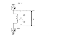
- FIG. 1A is a schematic diagram illustrating a state in which a motor voltage V is applied to a one-phase winding in normal control.
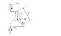
- FIG. 1B is a schematic diagram illustrating a state in which the motor voltage V is applied to the three-phase windings that are star-connected in the control at the time of abnormality.
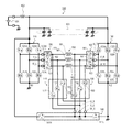
- FIG. 2 is a circuit diagram illustrating a circuit configuration of the power conversion apparatus 100 according to the exemplary embodiment 1.
- FIG. 3 is a circuit diagram illustrating a circuit configuration of the first phase separation relay circuit 150 according to the exemplary embodiment 1.
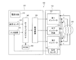
- FIG. 4 is a block diagram showing a typical block configuration of a motor drive unit 400 having the power conversion device 100.
- FIG. 5 exemplifies a current waveform obtained by plotting current values flowing through the U-phase, V-phase, and W-phase windings of the motor 200 when the power conversion device 100 is controlled according to the normal three-phase energization control. It is a graph.
- FIG. 6 is a circuit diagram illustrating a circuit configuration of a power conversion device 100A according to a modification of the exemplary embodiment 1.
- FIG. 7 is a circuit diagram illustrating a circuit configuration of a power conversion device 100B according to a further modification of the exemplary embodiment 1.
- FIG. 8 is a circuit diagram showing a circuit configuration of a power conversion device 100C according to an exemplary embodiment 2.
- FIG. 9 is a circuit diagram illustrating a circuit configuration of a power conversion device 100D according to an exemplary embodiment 3.
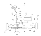
- FIG. 10 is a schematic diagram illustrating a typical configuration of an electric power steering apparatus 500 according to an exemplary embodiment 4.
- FIG. 1A schematically shows how the motor voltage V is applied to a single-phase winding in normal control.
- FIG. 1B schematically shows a state in which the motor voltage V is applied to the three-phase windings that are star-connected in the control at the time of abnormality.
- the normal control mode disclosed in Patent Document 1 has first to third control modes.
- the third control mode corresponds to three-phase energization control of the present disclosure described later.
- the voltage V is applied to the one-phase winding as it is.
- abnormal control the three-phase windings are star-connected, and the star-connected node functions as a neutral point.
- the voltage applied to the one-phase winding is V / (3) 1/2 .
- the voltage applied to the one-phase winding is reduced to 1 / (3) 1/2 compared to that at the time of normal, despite the same motor voltage as the control at the normal time. To do. As a result, the problem that motor output falls arises.
- the motor output (W) is obtained based on the torque (N ⁇ m) and the rotation speed (rpm).
- a power conversion device that converts power supplied to a three-phase motor having three-phase (U-phase, V-phase, and W-phase) windings as an example.
- a power conversion device that converts electric power supplied to an n-phase motor having n-phase windings (n is an integer of 4 or more) such as four-phase or five-phase is also included in the scope of the present disclosure.
- FIG. 2 schematically shows a circuit configuration of the power conversion apparatus 100 according to the present embodiment.
- the power conversion apparatus 100 includes first and second inverters 120 and 130, a sub inverter circuit 140, and first to fourth phase separation relay circuits 150, 160, 170, and 180.
- the power conversion device 100 is connected to the motor 200 and converts the power from the power source 101 into power supplied to the motor 200 having a three-phase winding.
- the motor 200 is, for example, a three-phase AC motor.
- the motor 200 has a U-phase winding M1, a V-phase winding M2, and a W-phase winding M3, and can be connected to the first inverter 120, the second inverter 130, and the sub-inverter circuit 140. is there. More specifically, the first inverter 120 can be connected to one end of the winding of each phase of the motor 200, and the second inverter 130 can be connected to the other end of the winding of each phase.
- the sub inverter circuit 140 can be connected to one end and the other end of each phase winding.
- “connection” between components (components) mainly means electrical connection.
- the first inverter 120 has U-phase, V-phase, and W-phase terminals U_L, V_L, and W_L.
- Second inverter 130 has U-phase, V-phase, and W-phase terminals U_R, V_R, and W_R.
- the sub-inverter circuit 140 has U-phase, V-phase, and W-phase terminals U_S, V_S, and W_S that are common to the first and second inverters 120 and 130.
- the terminal U_L of the first inverter 120 is connected to one end of the U-phase winding M1, the terminal V_L is connected to one end of the V-phase winding M2, and the terminal W_L is connected to one end of the W-phase winding M3. Connected. Similar to the first inverter 120, the terminal U_R of the second inverter 130 is connected to the other end of the winding M1, the terminal V_R is connected to the other end of the winding M2, and the terminal W_R is connected to the other end of the winding M3. Connected to the end.
- Such connection of the motor winding is different from so-called star connection and delta connection.
- the terminal U_S of the sub inverter circuit 140 can be connected to one end or the other end of the U-phase winding M1, the terminal V_S can be connected to one end or the other end of the V-phase winding M2, and the terminal W_S is , And can be connected to one end or the other end of the W-phase winding M3.
- the first inverter 120 (may be referred to as “bridge circuit L”) includes a bridge circuit composed of three legs. Each leg has a low-side switching element and a high-side switching element.
- Switching elements 121L, 122L, and 123L shown in FIG. 2 are low-side switching elements, and switching elements 121H, 122H, and 123H are high-side switching elements.
- a semiconductor switch element such as a field effect transistor (typically MOSFET) or an insulated gate bipolar transistor (IGBT) can be used.
- MOSFET field effect transistor
- IGBT insulated gate bipolar transistor
- the switching element may be expressed as an FET.
- the switching element 121L is denoted as FET 121L.
- the first inverter 120 uses, for example, a shunt resistor (not shown) provided in each leg as a current sensor 190 (see FIG. 4) for detecting the current flowing through the windings M1, M2, and M3 of each phase.
- the current sensor 190 has a current detection circuit (not shown) that detects a current flowing through the shunt resistor.
- the shunt resistor is connected between the low-side switching element and the node N1 on the GND side in each leg.
- the resistance value of the shunt resistor is, for example, about 0.5 m ⁇ to 1.0 m ⁇ .
- the second inverter 130 (may be referred to as “bridge circuit R”) includes a bridge circuit composed of three legs.
- FETs 131L, 132L, and 133L shown in FIG. 2 are low-side switching elements, and FETs 131H, 132H, and 133H are high-side switching elements.
- each leg of the second inverter 130 has a shunt resistor (not shown) like the first inverter 120.
- the shunt resistor is connected between the low-side switching element and the node N2 on the GND side in each leg.
- Each FET of the first and second inverters 120, 130 can be controlled by, for example, a microcontroller or a dedicated driver.
- the arrangement of the shunt resistors described above is an example, and the number of shunt resistors to be used and the arrangement thereof are appropriately determined in consideration of the product cost, design specifications, and the like.
- the sub-inverter circuit 140 has at least one leg.
- a circuit having at least one leg is referred to as a “sub inverter circuit”.
- the sub inverter circuit 140 according to the present embodiment has one leg having a high side switching element 141H and a low side switching element 141L.
- the leg may have a shunt resistance.
- Terminals U_S, V_S, and W_S of the sub inverter circuit 140 are terminals commonly connected to the node N3 between the high side switching element 141H and the low side switching element 141L.
- the first phase separation relay circuit 150 includes three first phase separation relays 151, 152, and 153 that switch connection and disconnection between one end of each phase winding and the first inverter 120.
- the first phase separation relay circuit 150 is connected between one end of each phase winding and the first inverter 120.
- the first phase separation relay 151 is connected between the terminal U_L of the first inverter 120 and one end of the U-phase winding M1.
- the first phase separation relay 152 is connected between the terminal V_L and one end of the V-phase winding M2.
- the first phase separation relay 153 is connected between the terminal W_L and one end of the W-phase winding M3.
- the first phase separation relay circuit 150 can switch connection and non-connection between one end of each phase winding and the first inverter 120 for each phase.
- the second phase separation relay circuit 160 includes three second phase separation relays 161, 162, and 163 that switch connection and non-connection between the other end of each phase winding and the second inverter 130.
- Second phase separation relay circuit 160 is connected between the other end of the winding of each phase and second inverter 130.
- the second phase separation relay 161 is connected between the terminal U_R of the second inverter 130 and the other end of the U-phase winding M1.
- the second phase separation relay 162 is connected between the terminal V_R and the other end of the V-phase winding M2.
- the second phase separation relay 163 is connected between the terminal W_R and the other end of the W-phase winding M3.
- the second phase separation relay circuit 160 can switch connection and disconnection between the other end of the winding of each phase and the second inverter 130 for each phase.
- the third phase separation relay circuit 170 includes three third phase separation relays 171, 172, and 173 that switch connection and disconnection between one end of the winding of each phase and the sub inverter circuit 140.
- Third phase separation relay circuit 170 is connected between one end of each phase winding and sub inverter circuit 140.
- the third phase separation relay 171 is connected between the terminal U_S of the sub inverter circuit 140 and one end of the U-phase winding M1.
- the first phase separation relay 172 is connected between the terminal V_S and one end of the V-phase winding M2.
- the third phase separation relay 173 is connected between the terminal W_S and one end of the W-phase winding M3.
- the third phase separation relay circuit 170 can switch connection and non-connection between one end of each phase winding and the sub inverter circuit 140 for each phase.
- the fourth phase separation relay circuit 180 includes three fourth phase separation relays 181, 182, and 183 that switch connection and non-connection between the other end of each phase winding and the sub inverter circuit 140.
- Fourth phase separation relay circuit 180 is connected between the other end of each phase winding and sub-inverter circuit 140.
- the fourth phase separation relay 181 is connected between the terminal U_S of the sub inverter circuit 140 and the other end of the U-phase winding M1.
- the fourth phase separation relay 182 is connected between the terminal V_S and the other end of the V-phase winding M2.
- the fourth phase separation relay 183 is connected between the terminal W_S and the other end of the W-phase winding M3.
- the fourth phase separation relay circuit 180 can switch connection and non-connection between the other end of the winding of each phase and the sub inverter circuit 140 for each phase.
- the first phase separation relay 151 and the third phase separation relay 171 are connected in common at one end of the U phase winding M1, and the first phase separation relay 152 and the third phase separation are connected.
- the relay 172 is commonly connected at one end of the V-phase winding M2, and the first phase separation relay 153 and the third phase separation relay 173 are commonly connected at one end of the W-phase winding M3.
- the second phase separation relay 161 and the fourth phase separation relay 181 are connected in common at the other end of the U-phase winding M1, and the second phase separation relay 162 and the fourth phase separation relay 181 are connected to each other.
- the phase separation relay 182 is commonly connected to the other end of the V-phase winding M2, and the second phase separation relay 163 and the fourth phase separation relay 183 are commonly used to the other end of the W-phase winding M3. Connected.
- the first phase separation relays 151, 152, 153, the second phase separation relays 161, 162, 163, the third phase separation relays 171, 172, 173, the fourth phase separation relays 181, 182 and 183 are turned on and off. For example, it can be controlled by a microcontroller or a dedicated driver. As these relays, for example, semiconductor switching elements such as FETs or IGBTs can be widely used. A mechanical relay may be used as the relay. In the present specification, an example in which FETs having freewheeling diodes are used as these relays will be described. In the following description, each relay is denoted as FET.
- the first phase separation relays 151, 152, and 153 are denoted as FETs 151, 152, and 153, respectively.
- the three FETs 151, 152, and 153 can be arranged such that the freewheeling diodes are directed in the same direction and forward current flows to the freewheeling diodes toward the motor 200.
- the three FETs 161, 162, and 163 can be arranged such that the free-wheeling diodes are directed in the same direction and forward current flows to the free-wheeling diodes toward the motor 200.
- the three FETs 171, 172, and 173 can be arranged such that the freewheeling diodes are directed in the same direction and forward current flows to the freewheeling diodes toward the motor 200.
- the three FETs 181, 182, and 183 can be arranged such that the freewheeling diodes are directed in the same direction, and forward current flows through the freewheeling diodes toward the motor 200. According to such an arrangement of the FET, the current flowing through the phase separation relay circuit in the off state can be cut off.
- FIG. 3 schematically shows a circuit configuration of a first phase separation relay circuit 150 having two FETs connected in series for each phase.
- the first phase separation relay circuit 150 may have a plurality of phase separation relays for each phase. As shown in FIG. 3, for example, the first phase separation relay circuit 150 may have two FETs connected in series for each phase. Two U-phase FETs 151A and 151B are arranged, two V-phase FETs 152A and 152B are arranged, and two W-phase FETs 153A and 153B are arranged. Further, the FETs 151A, 152A, and 153A can be arranged such that the free-wheeling diodes are directed in the same direction and forward current flows through the free-wheeling diodes toward the first inverter 120.
- the FETs 151B, 152B, and 153B can be arranged such that the free-wheeling diodes are directed in the same direction and forward current flows to the free-wheeling diodes toward the motor 200. According to such an arrangement of the FET, the current flowing through the phase separation relay circuit in the off state can be more reliably interrupted.
- the second, third and fourth phase separation relay circuits 160, 170 and 180 may have a plurality of phase separation relays for each phase.
- these phase separation relay circuits may have two FETs connected in series for each phase.
- the power conversion apparatus 100 is connected to a power source 101 and GND. Specifically, each of the first inverter 120, the second inverter 130, and the sub-inverter circuit 140 is connected to the power source 101 and GND. Power is supplied from the power source 101 to the first inverter 120, the second inverter 130, and the sub inverter circuit 140.
- the power supply 101 generates a predetermined power supply voltage.
- a DC power source is used as the power source 101.
- the power source 101 may be an AC-DC converter and a DC-DC converter, or may be a battery (storage battery).
- the power source 101 may be a single power source common to the first inverter 120, the second inverter 130, and the sub-inverter circuit 140, or the first power source for the first inverter 120 and the second power source for the second inverter 130. You may have two power supplies.
- a coil 102 is provided between the power source 101 and the power converter 100.
- the coil 102 functions as a noise filter, and smoothes the high frequency noise included in the voltage waveform supplied to each inverter or the high frequency noise generated by each inverter so as not to flow to the power source 101 side.
- a capacitor 103 is connected to the power supply terminals of the first inverter 120, the second inverter 130, and the sub inverter circuit 140.
- the capacitor 103 is a so-called bypass capacitor and suppresses voltage ripple.
- the capacitor 103 is, for example, an electrolytic capacitor, and the capacity and the number to be used are appropriately determined according to design specifications and the like.
- FIG. 4 schematically shows a typical block configuration of a motor drive unit 400 having the power conversion apparatus 100.
- the motor drive unit 400 includes the power conversion device 100, the motor 200, and the control circuit 300.
- the control circuit 300 includes, for example, a power supply circuit 310, an angle sensor 320, an input circuit 330, a microcontroller 340, a drive circuit 350, and a ROM 360.
- the control circuit 300 is connected to the power conversion device 100 and drives the motor 200 by controlling the power conversion device 100.
- the control circuit 300 can realize the closed loop control by controlling the target motor torque and rotation speed.
- the power supply circuit 310 generates a DC voltage (for example, 3V, 5V) necessary for each block in the circuit.
- the angle sensor 320 is, for example, a resolver or a Hall IC.
- the angle sensor 320 detects the rotation angle of the rotor of the motor 200 (hereinafter referred to as “rotation signal”) and outputs the rotation signal to the microcontroller 340.
- the input circuit 330 receives the motor current value detected by the current sensor 190 (hereinafter referred to as “actual current value”), and converts the level of the actual current value to the input level of the microcontroller 340 as necessary. Then, the actual current value is output to the microcontroller 340.
- the microcontroller 340 controls the switching operation (turn-on or turn-off) of each FET in the first inverter 120, the second inverter 130, and the sub inverter circuit 140 of the power conversion device 100.
- the microcontroller 340 sets the target current value according to the actual current value and the rotation signal of the rotor, generates a PWM signal, and outputs it to the drive circuit 350.
- the drive circuit 350 is typically a gate driver.
- the drive circuit 350 generates a control signal (gate control signal) for controlling the switching operation of each FET in the first inverter 120, the second inverter 130, and the sub inverter circuit 140 according to the PWM signal, and sends the control signal to the gate of each FET.
- the drive circuit 350 generates a gate control signal for controlling on / off of each FET in the first to fourth phase separation relay circuits 150, 160, 170, and 180 in accordance with an instruction from the microcontroller 340.
- a control signal can be applied to the gate.
- the microcontroller 340 may have the function of the drive circuit 350.
- the microcontroller 340 and the drive circuit 350 can be mounted on the same chip, for example.
- the ROM 360 is, for example, a writable memory (for example, PROM), a rewritable memory (for example, flash memory), or a read-only memory.
- the ROM 360 stores a control program including a command group for causing the microcontroller 340 to control the power conversion apparatus 100.
- the control program is temporarily expanded in a RAM (not shown) at the time of booting.
- the power conversion apparatus 100 has normal and abnormal control.
- the control circuit 300 (mainly the microcontroller 340) can switch the control of the power conversion apparatus 100 from normal control to abnormal control. Depending on the type of control, the on / off states of the FETs in the first to fourth phase separation relay circuits 150, 160, 170 and 180 are determined.
- the control circuit 300 selectively controls two FETs commonly connected to one end of each phase winding, and two FETs commonly connected to the other end of each phase winding. Alternatively. More specifically, the control circuit 300 turns on one of the two FETs 151 and 171 commonly connected to one end of the U-phase winding M1, and turns off the other. In addition, the control circuit 300 turns on one of the two FETs 161 and 181 commonly connected to the other end of the U-phase winding M1, and turns off the other. The control circuit 300 controls on / off of the remaining FETs connected to the V-phase winding M2 and the W-phase winding M3 in the same manner as the above control.
- one end of the U-phase winding M1 is connected to the first inverter 120. More specifically, one end of the U-phase winding M1 is connected to a node between the FETs 121H and 121L in the inverter circuit of the first inverter 120 via the FET 151 and the terminal U_L of the first inverter 120.
- one end of the U-phase winding M1 is connected to the sub inverter circuit 140. More specifically, one end of the U-phase winding M1 is connected to the node N3 of the sub inverter circuit 140 via the FET 171 and the terminal U_S of the sub inverter circuit 140.
- connection state of the V-phase winding M2, the first inverter 120, the second inverter 130, and the sub-inverter circuit 140 according to the on / off state of each FET is the same as that of the U-phase winding M1 described above. It is the same.
- connection state of the W-phase winding M3, the first inverter 120, the second inverter 130, and the sub-inverter circuit 140 according to the on / off state of each FET is also the same as that of the U-phase winding M1 described above. It is the same.
- turning on all the FETs in each phase separation relay circuit is referred to as “turning on the phase separation relay circuit”.
- turning off all the FETs in each phase separation relay circuit is referred to as “turning off the phase separation relay circuit”.
- turning on the first phase separation relay circuit 150 means turning on all of the FETs 151, 152, and 153, and turning off the first phase separation relay circuit 150 turns off all of the FETs 151, 152, and 153. Refers to that.
- the control circuit 300 turns on the first and second phase separation relay circuits 150 and 160 and turns off the third and fourth phase separation relay circuits 170 and 180.
- one end of each phase winding is connected to the first inverter 120, and the other end is connected to the second inverter 130.
- the sub inverter circuit 140 is electrically disconnected from one end and the other end of each phase winding.
- the control circuit 300 drives the motor 200 by performing three-phase energization control using both the first and second inverters 120 and 130.
- the H bridge including FETs 121L, 121H, 131L, and 131H
- FET 121L when FET 121L is turned on, FET 131L is turned off, and when FET 121L is turned off, FET 131L is turned on.
- FET 121H when the FET 121H is turned on, the FET 131H is turned off, and when the FET 121H is turned off, the FET 131H is turned on.
- FIG. 5 shows a current waveform (sine wave) obtained by plotting the current values flowing in the U-phase, V-phase, and W-phase windings of the motor 200 when the power conversion device 100 is controlled according to the normal three-phase energization control. ).
- the horizontal axis represents the motor electrical angle (deg), and the vertical axis represents the current value (A).
- the current value is plotted every 30 ° electrical angle.
- Ipk represents the maximum current value (peak current value) of each phase.
- Table 1 shows the value of current flowing through the terminals of each inverter for each electrical angle in the sine wave of FIG.
- Table 1 specifically shows the current value flowing through the terminals U_L, V_L and W_L of the first inverter 120 (bridge circuit L) at every electrical angle of 30 °, and the terminal U_R of the second inverter 130 (bridge circuit R).
- V_R and W_R current values for every electrical angle of 30 ° are shown.
- the direction of current flowing from the terminal of the bridge circuit L to the terminal of the bridge circuit R is defined as a positive direction.
- the direction of current shown in FIG. 5 follows this definition.
- the direction of current flowing from the terminal of the bridge circuit R to the terminal of the bridge circuit L is defined as a positive direction. Therefore, the phase difference between the current of the bridge circuit L and the current of the bridge circuit R is 180 °.
- the magnitude of the current value I 1 is [(3) 1/2 / 2] * I pk
- the magnitude of the current value I 2 is I pk / 2.
- the current magnitude I 2 flows from the bridge circuit L to the bridge circuit R is the winding M1 of the U-phase
- the size of the bridge circuit R is the winding M2 of the V-phase bridge circuit L I pk of current flows
- the current magnitude I 2 flows from the bridge circuit L to the bridge circuit R is the winding M3 of W-phase.
- the current magnitude I 1 flows from the bridge circuit L to the bridge circuit R is the winding M1 of the U-phase
- the size of the bridge circuit R is the winding M2 of the V-phase bridge circuit L I 1 current flows. No current flows through the W-phase winding M3.
- a current of magnitude I pk flows from the bridge circuit L to the bridge circuit R in the U-phase winding M1, and a magnitude I from the bridge circuit R to the bridge circuit L in the V-phase winding M2. 2 of current flows, the current magnitude I 2 flows from the bridge circuit R to the bridge circuit L is the winding M3 of W-phase.
- a current of magnitude I 1 flows from the bridge circuit L to the bridge circuit R in the U-phase winding M1, and a magnitude I from the bridge circuit R to the bridge circuit L in the W-phase winding M3. 1 current flows. No current flows through the V-phase winding M2.
- the current magnitude I 2 flows from the bridge circuit L to the bridge circuit R is the winding M1 of the U-phase
- the winding M2 of the V-phase bridge circuit L from the bridge circuit R to the magnitude I 2 flows
- a current of magnitude Ipk flows from the bridge circuit R to the bridge circuit L in the W-phase winding M3.
- the current magnitude I 2 flows from the bridge circuit R to the bridge circuit L is the winding M1 of the U-phase
- the current magnitude I 2 flows from the bridge circuit R to the bridge circuit L is the winding M3 of W-phase.
- a current of magnitude I 1 flows from the bridge circuit R to the bridge circuit L through the U-phase winding M1, and a magnitude I from the bridge circuit L to the bridge circuit R flows through the V-phase winding M2. 1 current flows. No current flows through the W-phase winding M3.
- a current of magnitude I pk flows through the U-phase winding M1 from the bridge circuit R to the bridge circuit L, and a magnitude I from the bridge circuit L to the bridge circuit R flows through the V-phase winding M2. 2 of current flows, the current magnitude I 2 flows from the bridge circuit L to the bridge circuit R is the winding M3 of W-phase.
- a current of magnitude I 1 flows from the bridge circuit R to the bridge circuit L through the U-phase winding M1, and a magnitude I from the bridge circuit L to the bridge circuit R flows through the W-phase winding M3. 1 current flows. No current flows through the V-phase winding M2.
- the current magnitude I 2 flows from the bridge circuit R to the bridge circuit L is the winding M1 of the U-phase
- the size of the bridge circuit R is the winding M2 of the V-phase bridge circuit L I 2 flows
- a current of magnitude Ipk flows from the bridge circuit L to the bridge circuit R in the W-phase winding M3.
- the control circuit 300 controls the switching operation of each FET of the bridge circuits L and R by PWM control that obtains the current waveform shown in FIG.
- the specific example of the control method at the time of abnormality of the power converter device 100 is demonstrated.
- the abnormality mainly means that a failure has occurred in the FET.
- the failure of the FET is roughly classified into “open failure” and “short failure”.
- Open failure refers to a failure in which the source and drain of the FET are opened (in other words, the resistance rds between the source and drain becomes high impedance)
- short failure refers to the failure between the source and drain of the FET. Refers to a short circuit failure.
- the present disclosure is mainly directed to a method for controlling the power conversion apparatus 100 when a random failure occurs. However, the present disclosure is also directed to a method for controlling the power conversion apparatus 100 in a case where a plurality of FETs are chained and failed.
- a chain failure means, for example, a failure that occurs simultaneously in a high-side switching element and a low-side switching element of one leg.
- random failure may occur. Note that random failures are different from manufacturing failures that may occur during manufacturing. If even one of the plurality of FETs in the two inverters fails, motor drive by normal three-phase energization control cannot be continued.
- the drive circuit 350 monitors the FET drain-source voltage Vds and compares the predetermined threshold voltage with Vds to detect the FET failure.
- the threshold voltage is set in the drive circuit 350 by, for example, data communication with an external IC (not shown) and external components.
- the drive circuit 350 is connected to a port of the microcontroller 340 and notifies the microcontroller 340 of a failure detection signal. For example, when detecting a failure of the FET, the drive circuit 350 asserts a failure detection signal.
- the microcontroller 340 receives the asserted failure detection signal, the microcontroller 340 reads internal data of the drive circuit 350 and determines which one of the plurality of FETs in the two inverters is faulty.
- the microcontroller 340 can also detect failure of the FET based on the difference between the actual current value of the motor and the target current value.
- failure detection is not limited to these methods, and known methods relating to failure detection can be widely used.
- the microcontroller 340 switches the control of the power conversion device 100 from normal control to abnormal control.
- the timing for switching control from normal to abnormal is about 10 msec to 30 msec after the failure detection signal is asserted.
- the control circuit 300 turns off the FET connected to the leg (of the bridge circuit R) including the failed FET among the three FETs 151, 152, and 153 in the first phase separation relay circuit 150, and other switching elements. Of the three FETs 171, 172, and 173 in the third phase separation relay circuit 170 and the FET commonly connected at one end of the winding of the first phase separation relay circuit 150. Turns on and turns off other switch elements.
- the control circuit 300 further turns on the second phase separation relay circuit 160 and turns off the fourth phase separation relay circuit 180. According to this control, the leg (node N3) of the sub-inverter circuit 140 can be electrically connected to one of the six ends of the windings M1 to M3.
- control when the high-side switching element (FET) 121H fails in the bridge circuit R of the first inverter 120 is exemplified.
- FET high-side switching element
- 123H, 121L, 122L, and 123L fail, based on the procedure shown below, control of the power converter device 100 can be switched to control at the time of abnormality.
- the control circuit 300 turns off the FET 151 connected to the leg (of the bridge circuit R) including the failed FET 121H among the FETs 151, 152, and 153 in the first phase separation relay circuit 150 and turns off the other FETs 152 and 153.
- the FET 171 that is turned off in the first phase separation relay circuit 150 and the FET 171 that is commonly connected to one end of the winding M1 are turned on in the third phase separation relay circuit 170.
- the other FETs 172 and 173 are turned off.
- the control circuit 300 further turns on the second phase separation relay circuit 160 and turns off the fourth phase separation relay circuit 180.
- the leg of the sub inverter circuit 140 is connected to one end of the winding M1.
- the leg including the failed FET 121H is electrically disconnected from one end of the winding M1, and instead, the leg of the sub inverter circuit 140 is connected to one end of the winding M1. In this way, the leg including the failed FET 121H in the bridge circuit R can be replaced with the leg of the sub inverter circuit 140.
- One end of the winding M1 is connected to the leg of the sub inverter circuit 140, one end of the windings M2 and M3 is connected to the leg of the first inverter 120, respectively, and the other end of the windings M1, M2, and M3 is , Connected to the second inverter 130.
- three-phase energization control is performed as in the normal state. Can be continued.
- the FETs of the first to fourth phase separation relay circuits 150, 160, 170, and 180 are connected in the same manner as in the control when the first inverter 120 fails.
- the leg including the failed FET in the bridge circuit L can be replaced with the leg of the sub inverter circuit 140. As a result, it is possible to continue the three-phase energization control.
- the three-phase energization control can be continued even when the control of the power conversion apparatus 100 is switched from the normal control to the abnormal control.
- the same motor output as in the normal state can be obtained in the control at the time of abnormality.
- FIG. 6 schematically shows a circuit configuration of a power conversion device 100A according to a modification of the present embodiment.
- sub inverter circuit 140 has two legs. At least one of one ends of the windings of each phase is a node between the low-side switching element and the high-side switching element in one of the two legs of the sub inverter circuit 140 via the third phase separation relay circuit 170. And the remaining one end of the windings of each phase is connected to the low-side switching element and the high-side switching element on the other of the two legs of the sub inverter circuit 140 via the third-phase separation relay circuit 170 Connected to the node between.
- At least one of the other ends of the windings of each phase is connected to a node in one leg of sub inverter circuit 140 via fourth phase separation relay circuit 180, and The rest of the other ends of the phase windings are connected to a node in the other leg of the sub-inverter circuit 140 via the fourth phase separation relay circuit 180.
- each winding can be connected to one of the two legs of the sub inverter circuit 140.
- the other end of each winding can be connected to one of the two legs of the sub-inverter circuit 140.
- FIG. 6 illustrates a configuration in which both ends of the winding M1 are connected to one leg of the sub inverter circuit 140 and both ends of the windings M2 and M3 are connected to the other leg.
- the connection example between the two legs of the sub inverter circuit 140 and both ends of each winding is not limited to this, and may be any selectable combination.
- the control circuit 300 turns off the FET 151 connected to the leg (of the bridge circuit R) including the failed FET 121H in the first phase separation relay circuit 150, turns on the FETs 152 and 153, and the third In the phase separation relay circuit 170, the FET 171 can be turned on and the FETs 172 and 173 can be turned off.
- the control circuit 300 further turns off the FET 162 connected to the leg (of the bridge circuit L) including the failed FET 132H in the second phase separation relay circuit 160, turns on the FETs 161 and 163, and the fourth phase.
- the FET 182 can be turned on and the FETs 181 and 183 can be turned off.
- the node N3 of one leg of the sub inverter circuit 140 is connected to one end of the winding M1, and the node N4 of the other leg is connected to the other end of the winding M2.
- three-phase energization control can be continued by replacing one leg in the bridge circuit R or L with one of the two legs of the sub inverter circuit 140. Furthermore, when there are two legs including a failed FET, the three-phase energization control can be continued by replacing those legs with two legs of the sub inverter circuit 140.
- FIG. 7 schematically shows a circuit configuration of a power conversion device 100B according to a further modification of the present embodiment.
- the sub inverter circuit 140 includes a first inverter leg and a second inverter leg. One end of each phase winding is connected to the node N3 in the first inverter leg of the sub inverter circuit 140 via the third phase separation relay circuit 170, and the other end of each phase winding is the fourth Via the phase separation relay circuit 180, the sub inverter circuit 140 is connected to the node N4 in the second inverter leg.
- one leg of the bridge circuit R is replaced with the first inverter leg of the sub inverter circuit 140, and one leg of the bridge circuit L is replaced with the second inverter of the sub inverter circuit 140. It becomes possible to replace it with a leg.
- the three-phase energization control can be continued.
- the power conversion device 100C according to the present embodiment is different from the power conversion device 100 according to the first embodiment in that the sub inverter circuit 140 has three legs.
- the sub inverter circuit 140 has three legs.
- FIG. 8 schematically shows a circuit configuration of the power conversion device 100C according to the present embodiment.
- the sub inverter circuit 140 has three legs.
- the terminal U_S of the sub inverter circuit 140 is connected to the node N3 between the FET 141H and the FET 141L, the terminal V_S is connected to the node N4 between the FET 142H and the FET 142L, and the terminal W_S is connected to the node N5 between the FET 143H and the FET 143L. Connected.
- each phase winding is connected to the three terminals U_S, V_S and W_S of the sub inverter circuit 140 via the third phase separation relay circuit 170.
- the other end of each phase winding is connected to the three terminals U_S, V_S and W_S of the sub inverter circuit 140 via the fourth phase separation relay circuit 180.
- the control at normal time and abnormal time is the three-phase energization control described in the first embodiment. Since the sub-inverter circuit 140 according to the present embodiment has three legs, it can be referred to as an “inverter” similarly to the first and second inverters 120 and 130. That is, the power conversion device 100C includes first to third inverters. According to this configuration, when one of the two inverters fails, the three-phase energization control can be continued using the inverter that has not failed and the sub-inverter circuit 140.
- the control circuit 300 turns off the first phase separation relay circuit 150, turns on the second phase separation relay circuit 160, turns on the third phase separation relay circuit 170, The four-phase separation relay circuit 180 may be turned off.
- the failed inverter can be disconnected from the motor 200, and the three-phase energization control can be continued using the second inverter 130 and the sub-inverter circuit 140.
- the three-phase energization control can be continued using the first inverter 120 and the sub-inverter circuit 140, similarly to the control described above.
- each FET of the phase separation relay circuit may be turned on / off for each phase as in the first embodiment.
- the control circuit 300 turns off the FET 151 in the first phase separation relay circuit 150, turns on the FETs 152 and 153, and turns on the FET 171 in the third phase separation relay circuit 170.
- the FETs 172 and 173 may be turned off. In other words, by using at least one of the three legs of the sub-inverter circuit 140, the three-phase energization control can be continued during an abnormality.
- the three-phase energization control is performed by replacing the entire bridge circuit R with the sub inverter circuit 140. It is possible to continue.
- the power conversion device 100D according to the present embodiment is different from the power conversion device 100 according to the first embodiment in that the motor 200 has two phase separation relay circuits only on the first inverter 120 side of the motor 200.
- FIG. 9 schematically shows a circuit configuration of the power conversion device 100D according to the present embodiment.
- the power conversion device 100D includes two phase separation relay circuits 150 and 170 only on the first inverter 120 side of the motor 200, that is, only on one side of the motor 200.
- the three-phase energization control is continued using the sub inverter circuit 140. be able to.
- a vehicle such as an automobile generally has an electric power steering device.
- the electric power steering apparatus generates an auxiliary torque for assisting a steering torque of a steering system that is generated when a driver operates a steering handle.
- the auxiliary torque is generated by the auxiliary torque mechanism, and the burden on the operation of the driver can be reduced.
- the auxiliary torque mechanism includes a steering torque sensor, an ECU, a motor, a speed reduction mechanism, and the like.
- the steering torque sensor detects steering torque in the steering system.
- the ECU generates a drive signal based on the detection signal of the steering torque sensor.
- the motor generates auxiliary torque corresponding to the steering torque based on the drive signal, and transmits the auxiliary torque to the steering system via the speed reduction mechanism.
- FIG. 10 schematically shows a typical configuration of the electric power steering apparatus 500 according to the present embodiment.
- the electric power steering apparatus 500 includes a steering system 520 and an auxiliary torque mechanism 540.
- the steering system 520 is, for example, a steering handle 521, a steering shaft 522 (also referred to as “steering column”), universal shaft joints 523A, 523B, and a rotating shaft 524 (also referred to as “pinion shaft” or “input shaft”). .), A rack and pinion mechanism 525, a rack shaft 526, left and right ball joints 552A and 552B, tie rods 527A and 527B, knuckle 528A and 528B, and left and right steering wheels (for example, left and right front wheels) 529A and 529B.
- the steering handle 521 is connected to the rotating shaft 524 via a steering shaft 522 and universal shaft joints 523A and 523B.
- a rack shaft 526 is connected to the rotation shaft 524 via a rack and pinion mechanism 525.
- the rack and pinion mechanism 525 includes a pinion 531 provided on the rotation shaft 524 and a rack 532 provided on the rack shaft 526.
- the right steering wheel 529A is connected to the right end of the rack shaft 526 through a ball joint 552A, a tie rod 527A, and a knuckle 528A in this order.
- the left steering wheel 529B is connected to the left end of the rack shaft 526 via a ball joint 552B, a tie rod 527B, and a knuckle 528B in this order.
- the right side and the left side correspond to the right side and the left side as viewed from the driver sitting on the seat, respectively.
- a steering torque is generated by the driver operating the steering handle 521, and is transmitted to the left and right steering wheels 529A and 529B via the rack and pinion mechanism 525. Accordingly, the driver can operate the left and right steering wheels 529A and 529B.
- the auxiliary torque mechanism 540 can be configured by, for example, a steering torque sensor 541, an ECU 542, a motor 543, a speed reduction mechanism 544, and a power conversion device 545.
- the auxiliary torque mechanism 540 gives auxiliary torque to the steering system 520 from the steering handle 521 to the left and right steering wheels 529A and 529B.
- the auxiliary torque may be referred to as “additional torque”.
- the control circuit 300 according to the present disclosure can be used as the ECU 542, and the power conversion device 100 according to the present disclosure can be used as the power conversion device 545.
- the motor 543 corresponds to the motor 200 in the present disclosure.
- the motor drive unit 400 according to the present disclosure can be suitably used as an electromechanically integrated motor that can be configured by the ECU 542, the motor 543, and the power conversion device 545.
- the steering torque sensor 541 detects the steering torque of the steering system 520 applied by the steering handle 521.
- the ECU 542 generates a drive signal for driving the motor 543 based on a detection signal from the steering torque sensor 541 (hereinafter referred to as “torque signal”).
- the motor 543 generates an auxiliary torque corresponding to the steering torque based on the drive signal.
- the auxiliary torque is transmitted to the rotating shaft 524 of the steering system 520 via the speed reduction mechanism 544.
- the speed reduction mechanism 544 is, for example, a worm gear mechanism.
- the auxiliary torque is further transmitted from the rotating shaft 524 to the rack and pinion mechanism 525.
- the electric power steering apparatus 500 can be classified into a pinion assist type, a rack assist type, a column assist type, and the like depending on a location where the assist torque is applied to the steering system 520.
- FIG. 10 shows a pinion assist type electric power steering apparatus 500.
- the electric power steering apparatus 500 is also applied to a rack assist type, a column assist type, and the like.
- the ECU 542 can receive not only a torque signal but also a vehicle speed signal, for example.
- the external device 560 is a vehicle speed sensor, for example.
- the external device 560 may be another ECU that can communicate via an in-vehicle network such as a CAN (Controller Area Network).
- the microcontroller of the ECU 542 can perform vector control or PWM control of the motor 543 based on a torque signal, a vehicle speed signal, and the like.
- the ECU 542 sets a target current value based on at least the torque signal.
- the ECU 542 preferably sets the target current value in consideration of the vehicle speed signal detected by the vehicle speed sensor and the rotor rotation signal detected by the angle sensor.
- the ECU 542 can control the drive signal of the motor 543, that is, the drive current so that the actual current value detected by the current sensor (not shown) matches the target current value.
- the left and right steering wheels 529A and 529B can be operated by the rack shaft 526 using the combined torque obtained by adding the auxiliary torque of the motor 543 to the steering torque of the driver.
- the motor drive unit 400 of the present disclosure for the above-described electromechanical integrated unit, the quality of the parts is improved, and the motor control can be performed even when the motor control is switched from normal control to abnormal control.
- An electric power steering apparatus having a motor drive unit capable of maintaining an output is provided.
- Embodiments of the present disclosure can be widely used in various devices having various motors such as a vacuum cleaner, a dryer, a ceiling fan, a washing machine, a refrigerator, and an electric power steering device.
- various motors such as a vacuum cleaner, a dryer, a ceiling fan, a washing machine, a refrigerator, and an electric power steering device.
- 100, 100A, 100B, 100C, 100D power conversion device 101: Power supply 102: Coil 103: Capacitor 120: First inverter 121H, 122H, 123H: High-side switching element (FET) 121L, 122L, 123L: Low-side switching element (FET) 130: second inverter 131H, 132H, 133H: High-side switching element (FET) 131L, 132L, 133L: Low-side switching element (FET) 140: Sub inverter circuit 150: First phase separation relay circuit 151, 152, 153: First phase separation relay (FET) 160: second phase separation relay circuit 161, 162, 163: second phase separation relay (FET) 170: Third phase separation relay circuit 171, 172, 173: third phase separation relay (FET) 180: Fourth phase separation relay circuit 181, 182, 183: Fourth phase separation relay (FET) 190: Current sensor 200: Electric motor 300: Control circuit 310: power supply circuit 320: Angle sensor 330:
Landscapes
- Engineering & Computer Science (AREA)
- Power Engineering (AREA)
- Chemical & Material Sciences (AREA)
- Combustion & Propulsion (AREA)
- Transportation (AREA)
- Mechanical Engineering (AREA)
- Control Of Ac Motors In General (AREA)
- Inverter Devices (AREA)
Abstract
【課題】モータ制御を正常時の制御から異常時の制御に切替えても、モータ出力を維持することが可能な電力変換装置を提供する。【解決手段】電力変換装置100は、モータ200の各相の巻線の一端に接続される第1インバータ120と、各相の巻線の他端に接続される第2インバータ130と、各相の巻線の一端と第1インバータとの接続および非接続を切替える第1相分離リレー回路150と、各相の巻線の他端と第2インバータとの接続および非接続を切替える第2相分離リレー回路160と、各相の巻線の一端および他端に接続可能であるサブインバータ回路140と、各相の巻線の一端とサブインバータ回路との接続および非接続を切替える第3相分離リレー回路170と、各相の巻線の他端とサブインバータ回路との接続および非接続を切替える第4相分離リレー回路180と、を有する。
Description
本開示は、電力変換装置、モータ駆動ユニットおよび電動パワーステアリング装置に関する。
ブラシレスDCモータおよび交流同期モータなどの電動モータ(以下、単に「モータ」と表記する。)は、一般的に三相電流によって駆動される。三相電流の波形を正確に制御するため、ベクトル制御などの複雑な制御技術が用いられる。このような制御技術では、高度な数学的演算が必要であり、マイクロコントローラ(マイコン)などのデジタル演算回路が用いられる。ベクトル制御技術は、モータの負荷変動が大きな用途、例えば、洗濯機、電動アシスト自転車、電動スクータ、電動パワーステアリング装置、電気自動車、産業機器などの分野で活用されている。一方、出力が相対的に小さなモータでは、パルス幅変調(PWM)方式などの他のモータ制御方式が採用されている。
車載分野においては、自動車用電子制御ユニット(ECU:Electrical Contorl Unit)が車両に用いられる。ECUは、マイクロコントローラ、電源、入出力回路、ADコンバータ、負荷駆動回路およびROM(Read Only Memory)などを有する。ECUを核として電子制御システムが構築される。例えば、ECUはセンサからの信号を処理してモータなどのアクチュエータを制御する。具体的に説明すると、ECUはモータの回転速度およびトルクを監視しながら、電力変換装置におけるインバータを制御する。ECUの制御の下で、電力変換装置はモータに供給する駆動電力を変換する。
近年、モータ、電力変換装置およびECUが一体化された機電一体型モータが開発されている。特に車載分野においては、安全性の観点から高い品質保証が要求される。そのため、部品の一部が故障した場合でも安全動作を継続できる冗長設計が取り入れられている。冗長設計の一例として、1つのモータに対して2つの電力変換装置を設けることが検討されている。他の一例として、メインのマイクロコントローラにバックアップ用マイクロコントローラを設けることが検討されている。
例えば特許文献1は、制御部と、2つのインバータとを有し、三相モータに供給する電力を変換する電力変換装置を開示している。2つのインバータの各々は電源およびグランド(以下、「GND」と表記する。)に接続される。一方のインバータは、モータの三相の巻線の一端に接続され、他方のインバータは、三相の巻線の他端に接続される。各インバータは、各々がハイサイドスイッチング素子およびローサイドスイッチング素子を含む3つのレグから構成されるブリッジ回路を有する。制御部は、2つのインバータにおけるスイッチング素子の故障を検出した場合、モータ制御を正常時の制御から異常時の制御に切替える。本明細書において、「異常」とは、主としてスイッチング素子の故障を意味する。また、「正常時の制御」は、全てのスイッチング素子が正常な状態における制御を意味し、「異常時の制御」は、あるスイッチング素子に故障が生じた状態における制御を意味する。
異常時の制御において、2つのインバータのうちの故障したスイッチング素子を含むインバータ(以下、「故障インバータ」と表記する。)には、スイッチング素子を所定の規則でオンまたはオフすることにより巻線の中性点が構成される。その規則によれば、例えば、ハイサイドスイッチング素子が常時オフとなるオープン故障が発生した場合、インバータのブリッジ回路において、3つのハイサイドスイッチング素子のうちの故障したスイッチング素子以外のものはオフし、かつ、3つのローサイドスイッチング素子はオンする。その場合、中性点はローサイド側に構成される。または、ハイサイドスイッチング素子が常時オンとなるショート故障が発生した場合、インバータのブリッジ回路において、3つのハイサイドスイッチング素子のうちの故障したスイッチング素子以外のものはオンし、かつ、3つのローサイドスイッチング素子はオフする。その場合、中性点はハイサイド側に構成される。特許文献1の電力変換装置によれば、異常時において、三相の巻線の中性点は、故障インバータの中に構成される。スイッチング素子に故障が生じても、正常な方のインバータを用いてモータ駆動を継続させることができる。
上述した従来の技術では、異常時の制御においてモータ出力のさらなる向上が求められていた。
本開示の実施形態は、モータ制御を正常時の制御から異常時の制御に切替えても、モータ出力を維持することが可能な電力変換装置を提供する。
本開示の例示的な電力変換装置は、電源からの電力を、n相(nは3以上の整数)の巻線を有するモータに供給する電力に変換する電力変換装置であって、前記モータの各相の巻線の一端に接続される第1インバータと、前記各相の巻線の他端に接続される第2インバータと、前記各相の巻線の一端と前記第1インバータとの接続および非接続を切替える第1相分離リレー回路と、前記各相の巻線の他端と前記第2インバータとの接続および非接続を切替える第2相分離リレー回路と、前記各相の巻線の一端および他端に接続可能であるサブインバータ回路と、前記各相の巻線の一端と前記サブインバータ回路との接続および非接続を切替える第3相分離リレー回路と、前記各相の巻線の他端と前記サブインバータ回路との接続および非接続を切替える第4相分離リレー回路と、を有する。
本開示の例示的な他の電力変換装置は、電源からの電力を、n相(nは3以上の整数)の巻線を有するモータに供給する電力に変換する電力変換装置であって、前記モータの各相の巻線の一端に接続される第1インバータと、前記各相の巻線の他端に接続される第2インバータと、前記各相の巻線の一端と前記第1インバータとの接続および非接続を切替える第1相分離リレー回路と、前記各相の巻線の一端に接続可能であるサブインバータ回路と、前記各相の巻線の一端と前記サブインバータ回路との接続および非接続を切替える第2相分離リレー回路と、を有する。
本開示の例示的な実施形態によると、モータ制御を正常時の制御から異常時の制御に切替えても、モータ出力を維持することが可能な電力変換装置、当該電力変換装置を有するモータ駆動ユニットおよび当該モータ駆動ユニットを有する電動パワーステアリング装置が提供される。
本開示の実施形態を説明する前に、本開示の基礎となった本願発明者の知見を説明する。
図1Aは、正常時の制御において一相の巻線にモータ電圧Vが印加される様子を模式的に示す。図1Bは、異常時の制御においてスター結線された3相の巻線にモータ電圧Vが印加される様子を模式的に示す。
特許文献1に開示された電力変換装置において、モータに電圧Vを印加することを考える。特許文献1に開示された正常時の制御モードは、第1から第3の制御モードを有する。なお、第3の制御モードは、後述する本開示の三相通電制御に相当する。第3の制御モードにおいて、図1Aに示されるように一相の巻線には電圧Vがそのまま印加される。一方で、異常時の制御において、三相の巻線はスター結線され、スター結線のノードが中性点として機能する。そのノードを中心に120°間隔で並ぶ三相の巻線を考える。その場合、図1Bに示されるように、一相の巻線に印加される電圧はV/(3)1/2となる。このように、異常時の制御では、正常時の制御と同じモータ電圧にもかかわらず、一相の巻線に印加される電圧は、正常時のそれと比べ1/(3)1/2に低下する。その結果、モータ出力が低下するといった課題が生じる。なお、モータ出力(W)は、トルク(N・m)および回転速度(rpm)に基づいて求められる。
以下、添付の図面を参照しながら、本開示の電力変換装置、モータ駆動ユニットおよび電動パワーステアリング装置の実施形態を詳細に説明する。但し、以下の説明が不必要に冗長になるのを避け、当業者の理解を容易にするため、必要以上に詳細な説明は省略する場合がある。例えば、既によく知られた事項の詳細説明や実質的に同一の構成に対する重複説明を省略する場合がある。
本願明細書においては、三相(U相、V相、W相)の巻線を有する三相モータに供給する電力を変換する電力変換装置を例にして、本開示の実施形態を説明する。ただし、四相または五相などのn相(nは4以上の整数)の巻線を有するn相モータに供給する電力を変換する電力変換装置も本開示の範疇である。
(実施形態1)
〔1.1.電力変換装置100の構造〕
図2は、本実施形態による電力変換装置100の回路構成を模式的に示す。
電力変換装置100は、第1および第2インバータ120、130と、サブインバータ回路140と、第1から第4相分離リレー回路150、160、170および180と、を有する。電力変換装置100は、モータ200に接続され、電源101からの電力を、三相の巻線を有するモータ200に供給する電力に変換する。
モータ200は、例えば三相交流モータである。モータ200は、U相の巻線M1、V相の巻線M2およびW相の巻線M3を有し、第1インバータ120と、第2インバータ130と、サブインバータ回路140と、に接続可能である。具体的に説明すると、第1インバータ120はモータ200の各相の巻線の一端に接続可能であり、第2インバータ130は各相の巻線の他端に接続可能である。サブインバータ回路140は、各相の巻線の一端および他端に接続可能である。本願明細書において、部品(構成要素)同士の間の「接続」は、主に電気的な接続を意味する。
第1インバータ120は、U相、V相およびW相の端子U_L、V_LおよびW_Lを有する。第2インバータ130は、U相、V相およびW相の端子U_R、V_RおよびW_Rを有する。サブインバータ回路140は、第1および第2インバータ120、130に共通の、U相、V相およびW相の端子U_S、V_SおよびW_Sを有する。
第1インバータ120の端子U_Lは、U相の巻線M1の一端に接続され、端子V_Lは、V相の巻線M2の一端に接続され、端子W_Lは、W相の巻線M3の一端に接続される。第1インバータ120と同様に、第2インバータ130の端子U_Rは、巻線M1の他端に接続され、端子V_Rは、巻線M2の他端に接続され、端子W_Rは、巻線M3の他端に接続される。モータ巻線のこのような結線は、いわゆるスター結線およびデルタ結線とは異なる。
サブインバータ回路140の端子U_Sは、U相の巻線M1の一端または他端に接続可能であり、端子V_Sは、V相の巻線M2の一端または他端に接続可能であり、端子W_Sは、W相の巻線M3の一端または他端に接続可能である。
第1インバータ120(「ブリッジ回路L」と表記する場合がある。)は、3個のレグから構成されるブリッジ回路を含む。各レグは、ローサイドスイッチング素子およびハイサイドスイッチング素子を有する。図2に示されるスイッチング素子121L、122Lおよび123Lがローサイドスイッチング素子であり、スイッチング素子121H、122Hおよび123Hがハイサイドスイッチング素子である。スイッチング素子として、例えば電界効果トランジスタ(典型的にはMOSFET)または絶縁ゲートバイポーラトランジスタ(IGBT)などの半導体スイッチ素子を用いることができる。本明細書において、インバータのスイッチング素子としてFETを用いる例を説明し、以下の説明ではスイッチング素子をFETと表記する場合がある。例えば、スイッチング素子121LはFET121Lと表記される。
第1インバータ120は、各相の巻線M1、M2およびM3に流れる電流を検出するための電流センサ190(図4を参照)として、例えば、各レグに設けられたシャント抵抗(不図示)を有する。電流センサ190は、シャント抵抗に流れる電流を検出する電流検出回路(不図示)を有する。例えば、シャント抵抗は、各レグにおいてローサイドスイッチング素子およびGND側のノードN1との間に接続される。シャント抵抗の抵抗値は、例えば0.5mΩ~1.0mΩ程度である。
第1インバータ120と同様に、第2インバータ130(「ブリッジ回路R」と表記する場合がある。)は、3個のレグから構成されるブリッジ回路を含む。図2に示されるFET131L、132Lおよび133Lがローサイドスイッチング素子であり、FET131H、132Hおよび133Hがハイサイドスイッチング素子である。また、第2インバータ130の各レグは、第1インバータ120と同様に、シャント抵抗(不図示)を有する。例えば、シャント抵抗は、各レグにおいてローサイドスイッチング素子およびGND側のノードN2との間に接続される。第1および第2インバータ120、130の各FETは、例えばマイクロコントローラまたは専用ドライバによって制御され得る。なお、上述したシャント抵抗の配置は一例であり、使用するシャント抵抗の数およびその配置は、製品コストおよび設計仕様などを考慮して適宜決定される。
本開示によるサブインバータ回路140は、少なくとも1つのレグを有する。本明細書では、少なくとも1つのレグを有する回路を「サブインバータ回路」と呼ぶこととする。本実施形態によるサブインバータ回路140は、ハイサイドスイッチング素子141Hおよびローサイドスイッチング素子141Lを有するレグを1個有する。そのレグは、シャント抵抗を有していてもよい。
サブインバータ回路140の端子U_S、V_SおよびW_Sは、ハイサイドスイッチング素子141Hおよびローサイドスイッチング素子141Lの間のノードN3に共通に接続された端子である。
第1相分離リレー回路150は、各相の巻線の一端と第1インバータ120との接続および非接続を切替える3個の第1相分離リレー151、152および153を有する。第1相分離リレー回路150は、各相の巻線の一端と第1インバータ120との間に接続される。具体的には、第1相分離リレー151は、第1インバータ120の端子U_LとU相の巻線M1の一端との間に接続される。第1相分離リレー152は、端子V_LとV相の巻線M2の一端との間に接続される。第1相分離リレー153は、端子W_LとW相の巻線M3の一端との間に接続される。第1相分離リレー回路150は、各相の巻線の一端と第1インバータ120との接続および非接続を相毎に切替えることが可能である。
第2相分離リレー回路160は、各相の巻線の他端と第2インバータ130との接続および非接続を切替える3個の第2相分離リレー161、162および163を有する。第2相分離リレー回路160は、各相の巻線の他端と第2インバータ130との間に接続される。具体的には、第2相分離リレー161は、第2インバータ130の端子U_RとU相の巻線M1の他端との間に接続される。第2相分離リレー162は、端子V_RとV相の巻線M2の他端との間に接続される。第2相分離リレー163は、端子W_RとW相の巻線M3の他端との間に接続される。第2相分離リレー回路160は、各相の巻線の他端と第2インバータ130との接続および非接続を相毎に切替えることが可能である。
第3相分離リレー回路170は、各相の巻線の一端とサブインバータ回路140との接続および非接続を切替える3個の第3相分離リレー171、172および173を有する。第3相分離リレー回路170は、各相の巻線の一端とサブインバータ回路140との間に接続される。具体的には、第3相分離リレー171は、サブインバータ回路140の端子U_SとU相の巻線M1の一端との間に接続される。第1相分離リレー172は、端子V_SとV相の巻線M2の一端との間に接続される。第3相分離リレー173は、端子W_SとW相の巻線M3の一端との間に接続される。第3相分離リレー回路170は、各相の巻線の一端とサブインバータ回路140との接続および非接続を相毎に切替えることが可能である。
第4相分離リレー回路180は、各相の巻線の他端とサブインバータ回路140との接続および非接続を切替える3個の第4相分離リレー181、182および183を有する。第4相分離リレー回路180は、各相の巻線の他端とサブインバータ回路140との間に接続される。具体的には、第4相分離リレー181は、サブインバータ回路140の端子U_SとU相の巻線M1の他端との間に接続される。第4相分離リレー182は、端子V_SとV相の巻線M2の他端との間に接続される。第4相分離リレー183は、端子W_SとW相の巻線M3の他端との間に接続される。第4相分離リレー回路180は、各相の巻線の他端とサブインバータ回路140との接続および非接続を相毎に切替えることが可能である。
巻線の一端側に着目すると、第1相分離リレー151と第3相分離リレー171とは、U相の巻線M1の一端で共通に接続され、第1相分離リレー152と第3相分離リレー172とは、V相の巻線M2の一端で共通に接続され、第1相分離リレー153と第3相分離リレー173とは、W相の巻線M3の一端で共通に接続される。
巻線の他端側に着目すると、第2相分離リレー161と第4相分離リレー181とは、U相の巻線M1の他端で共通に接続され、第2相分離リレー162と第4相分離リレー182とは、V相の巻線M2の他端で共通に接続され、第2相分離リレー163と第4相分離リレー183とは、W相の巻線M3の他端で共通に接続される。
第1相分離リレー151、152、153、第2相分離リレー161、162、163、第3相分離リレー171、172、173、第4相分離リレー181、182および183のリレーのオンおよびオフは、例えばマイクロコントローラまたは専用ドライバによって制御され得る。これらのリレーとして、例えばFETまたはIGBTなどの半導体スイッチ素子を広く用いることができる。また、リレーとして、メカニカルリレーを用いても構わない。本明細書において、これらのリレーとして還流ダイオードを有するFETを用いる例を説明し、以下の説明では、各リレーをFETと表記する。例えば、第1相分離リレー151、152および153は、FET151、152および153とそれぞれ表記される。
一例として、第1相分離リレー回路150において、3個のFET151、152および153は、還流ダイオードが同一方向を向き、かつ、モータ200に向けて順方向電流が還流ダイオードに流れるよう配置され得る。第2相分離リレー回路160において、3個のFET161、162および163は、還流ダイオードが同一方向を向き、かつ、モータ200に向けて順方向電流が還流ダイオードに流れるよう配置され得る。第3相分離リレー回路170において、3個のFET171、172および173は、還流ダイオードが同一方向を向き、かつ、モータ200に向けて順方向電流が還流ダイオードに流れるよう配置され得る。第4相分離リレー回路180において、3個のFET181、182および183は、還流ダイオードが同一方向を向き、かつ、モータ200に向けて順方向電流が還流ダイオードに流れるよう配置され得る。このようなFETの配置によると、オフ状態の相分離リレー回路に流れる電流を遮断することができる。
図3は、直列に接続された2つのFETを相毎に有する第1相分離リレー回路150の回路構成を模式的に示す。
他の一例として、第1相分離リレー回路150は、複数の相分離リレーを相毎に有していてもよい。図3に示されるように、例えば、第1相分離リレー回路150は、直列に接続された2つFETを相毎に有し得る。2つのU相用FET151A、151Bが配置され、2つのV相用FET152A、152Bが配置され、2つのW相用FET153A、153Bが配置される。また、FET151A、152Aおよび153Aは、還流ダイオードが同一方向を向き、かつ、第1インバータ120に向けて順方向電流が還流ダイオードに流れるよう配置され得る。一方、FET151B、152Bおよび153Bは、還流ダイオードが同一方向を向き、かつ、モータ200に向けて順方向電流が還流ダイオードに流れるよう配置され得る。このようなFETの配置によると、オフ状態の相分離リレー回路に流れる電流をより確実に遮断することができる。
第2、第3および第4相分離リレー回路160、170および180は、第1相分離リレー回路150と同様に、複数の相分離リレーを相毎に有していてもよい。例えば、これらの相分離リレー回路は、直列に接続された2つのFETを相毎に有し得る。
電力変換装置100は、電源101とGNDとに接続される。具体的に説明すると、第1インバータ120、第2インバータ130およびサブインバータ回路140の各々は、電源101およびGNDに接続される。第1インバータ120、第2インバータ130およびサブインバータ回路140に電力が電源101から供給される。
電源101は所定の電源電圧を生成する。電源101として、例えば直流電源が用いられる。ただし、電源101は、AC-DCコンバータおよびDC―DCコンバータであってもよいし、バッテリー(蓄電池)であってもよい。例えば、電源101は、第1インバータ120、第2インバータ130およびサブインバータ回路140に共通の単一電源であってもよいし、第1インバータ120用の第1電源および第2インバータ130用の第2電源を有していてもよい。
電源101と電力変換装置100との間にコイル102が設けられている。コイル102は、ノイズフィルタとして機能し、各インバータに供給する電圧波形に含まれる高周波ノイズ、または各インバータで発生する高周波ノイズを電源101側に流出させないように平滑化する。また、第1インバータ120、第2インバータ130およびサブインバータ回路140の電源端子には、コンデンサ103が接続されている。コンデンサ103は、いわゆるバイパスコンデンサであり、電圧リプルを抑制する。コンデンサ103は、例えば電解コンデンサであり、容量および使用する個数は設計仕様などによって適宜決定される。
〔1.2.モータ駆動ユニット400の構造〕
図4は、電力変換装置100を有するモータ駆動ユニット400の典型的なブロック構成を模式的に示す。
モータ駆動ユニット400は、電力変換装置100、モータ200および制御回路300を有する。
制御回路300は、例えば、電源回路310と、角度センサ320と、入力回路330と、マイクロコントローラ340と、駆動回路350と、ROM360とを有する。制御回路300は、電力変換装置100に接続され、電力変換装置100を制御することによりモータ200を駆動する。例えば、制御回路300は、目的とするモータトルクおよび回転速度を制御してクローズドループ制御を実現することができる。
電源回路310は、回路内の各ブロックに必要なDC電圧(例えば3V、5V)を生成する。角度センサ320は、例えばレゾルバまたはホールICである。角度センサ320は、モータ200のロータの回転角(以下、「回転信号」と表記する。)を検出し、回転信号をマイクロコントローラ340に出力する。入力回路330は、電流センサ190によって検出されたモータ電流値(以下、「実電流値」と表記する。)を受け取って、実電流値のレベルをマイクロコントローラ340の入力レベルに必要に応じて変換し、実電流値をマイクロコントローラ340に出力する。
マイクロコントローラ340は、電力変換装置100の第1インバータ120、第2インバータ130およびサブインバータ回路140における各FETのスイッチング動作(ターンオンまたはターンオフ)を制御する。マイクロコントローラ340は、実電流値およびロータの回転信号などに従って目標電流値を設定してPWM信号を生成し、それを駆動回路350に出力する。
駆動回路350は、典型的にはゲートドライバである。駆動回路350は、第1インバータ120、第2インバータ130およびサブインバータ回路140における各FETのスイッチング動作を制御する制御信号(ゲート制御信号)をPWM信号に従って生成し、各FETのゲートに制御信号を与える。また、駆動回路350は、第1から第4相分離リレー回路150、160、170および180における各FETのオンまたはオフを制御するゲート制御信号をマイクロコントローラ340からの指示に従って生成し、各FETのゲートに制御信号を与えることができる。なお、マイクロコントローラ340は駆動回路350の機能を有していてもよい。マイクロコントローラ340および駆動回路350は、例えば同一のチップに実装され得る。
ROM360は、例えば書き込み可能なメモリ(例えばPROM)、書き換え可能なメモリ(例えばフラッシュメモリ)または読み出し専用のメモリである。ROM360は、マイクロコントローラ340に電力変換装置100を制御させるための命令群を含む制御プログラムを格納する。例えば、制御プログラムはブート時にRAM(不図示)に一旦展開される。
〔1.3.電力変換装置100の制御〕
電力変換装置100には正常時および異常時の制御がある。制御回路300(主としてマイクロコントローラ340)は、電力変換装置100の制御を正常時の制御から異常時の制御に切替えることが可能である。制御の種類に応じて、第1から第4相分離リレー回路150、160、170および180の中の各FETのオン・オフ状態が決定される。
本実施形態による制御回路300は、各相の巻線の一端に共通に接続された2つのFETを択一的に制御し、各相の巻線の他端に共通に接続された2つのFETを択一的に制御する。具体的に説明すると、制御回路300は、U相の巻線M1の一端に共通に接続された2つのFET151、171のうちの一方をオンして他方をオフする。また、制御回路300は、U相の巻線M1の他端に共通に接続された2つのFET161、181のうちの一方をオンして他方をオフする。制御回路300は、V相の巻線M2およびW相の巻線M3に接続された残りのFETのオン・オフを、上記の制御と同様に制御する。
例えば、FET151がオン状態であり、FET171がオフ状態であるとき、U相の巻線M1の一端は、第1インバータ120に接続される。より詳細には、U相の巻線M1の一端は、FET151および第1インバータ120の端子U_Lを介して、第1インバータ120のインバータ回路の中のFET121Hおよび121Lの間のノードに接続される。これに対し、FET151がオフ状態であり、FET171がオン状態であるとき、U相の巻線M1の一端は、サブインバータ回路140に接続される。より詳細には、U相の巻線M1の一端は、FET171およびサブインバータ回路140の端子U_Sを介して、サブインバータ回路140のノードN3に接続される。
各FETのオン・オフ状態に応じた、V相の巻線M2と、第1インバータ120、第2インバータ130およびサブインバータ回路140と、の接続状態は、上述したU相の巻線M1のそれと同様である。各FETのオン・オフ状態に応じた、W相の巻線M3と、第1インバータ120、第2インバータ130およびサブインバータ回路140と、の接続状態も、上述したU相の巻線M1のそれと同様である。
本明細書において、各相分離リレー回路の中の全てのFETをオンすることを、「相分離リレー回路をオンする」と称することとする。また、各相分離リレー回路の中の全てのFETをオフすることを、「相分離リレー回路をオフする」と称することとする。例えば、第1相分離リレー回路150をオンするとは、FET151、152および153の全てをオンすることを指し、第1相分離リレー回路150をオフするとは、FET151、152および153の全てをオフすることを指す。
(1.3.1.正常時の制御)
電力変換装置100の正常時の制御方法の具体例を説明する。上述したとおり、正常とは、第1および第2インバータ120、130の各FETに故障が生じていない状態を指す。
正常時において、制御回路300は、第1および第2相分離リレー回路150、160をオンし、第3および第4相分離リレー回路170、180をオフする。これにより、各相の巻線の一端は、第1インバータ120に接続され、他端は、第2インバータ130に接続される。サブインバータ回路140は、各相の巻線の一端および他端から電気的に切り離される。この接続状態において、制御回路300は、第1および第2インバータ120、130の両方を用いて三相通電制御することによってモータ200を駆動する。具体的に、制御回路300は、第1インバータ120のFETと第2インバータ130のFETとを互いに逆位相(位相差=180°)でスイッチング制御することにより三相通電制御を行う。例えば、FET121L、121H、131Lおよび131Hを含むHブリッジに着目すると、FET121Lがオンすると、FET131Lはオフし、FET121Lがオフすると、FET131Lはオンする。これと同様に、FET121Hがオンすると、FET131Hはオフし、FET121Hがオフすると、FET131Hはオンする。
図5は、正常時の三相通電制御に従って電力変換装置100を制御したときにモータ200のU相、V相およびW相の各巻線に流れる電流値をプロットして得られる電流波形(正弦波)を例示する。横軸は、モータ電気角(deg)を示し、縦軸は電流値(A)を示す。図5の電流波形において、電気角30°毎に電流値をプロットしている。Ipkは各相の最大電流値(ピーク電流値)を表す。なお、図5に例示した正弦波以外に、例えば矩形波を用いてモータ200を駆動することは可能である。
表1は、図5の正弦波において電気角毎に、各インバータの端子に流れる電流値を示している。表1は、具体的に、第1インバータ120(ブリッジ回路L)の端子U_L、V_LおよびW_Lに流れる、電気角30°毎の電流値、および、第2インバータ130(ブリッジ回路R)の端子U_R、V_RおよびW_Rに流れる、電気角30°毎の電流値を示している。ここで、ブリッジ回路Lに対しては、ブリッジ回路Lの端子からブリッジ回路Rの端子に流れる電流方向を正の方向と定義する。図5に示される電流の向きはこの定義に従う。また、ブリッジ回路Rに対しては、ブリッジ回路Rの端子からブリッジ回路Lの端子に流れる電流方向を正の方向と定義する。従って、ブリッジ回路Lの電流とブリッジ回路Rの電流との位相差は180°となる。表1において、電流値I1の大きさは〔(3)1/2/2〕*Ipkであり、電流値I2の大きさはIpk/2である。

電気角0°において、U相の巻線M1には電流は流れない。V相の巻線M2にはブリッジ回路Rからブリッジ回路Lに大きさI1の電流が流れ、W相の巻線M3にはブリッジ回路Lからブリッジ回路Rに大きさI1の電流が流れる。
電気角30°において、U相の巻線M1にはブリッジ回路Lからブリッジ回路Rに大きさI2の電流が流れ、V相の巻線M2にはブリッジ回路Rからブリッジ回路Lに大きさIpkの電流が流れ、W相の巻線M3にはブリッジ回路Lからブリッジ回路Rに大きさI2の電流が流れる。
電気角60°において、U相の巻線M1にはブリッジ回路Lからブリッジ回路Rに大きさI1の電流が流れ、V相の巻線M2にはブリッジ回路Rからブリッジ回路Lに大きさI1の電流が流れる。W相の巻線M3には電流は流れない。
電気角90°において、U相の巻線M1にはブリッジ回路Lからブリッジ回路Rに大きさIpkの電流が流れ、V相の巻線M2にはブリッジ回路Rからブリッジ回路Lに大きさI2の電流が流れ、W相の巻線M3にはブリッジ回路Rからブリッジ回路Lに大きさI2の電流が流れる。
電気角120°において、U相の巻線M1にはブリッジ回路Lからブリッジ回路Rに大きさI1の電流が流れ、W相の巻線M3にはブリッジ回路Rからブリッジ回路Lに大きさI1の電流が流れる。V相の巻線M2には電流は流れない。
電気角150°において、U相の巻線M1にはブリッジ回路Lからブリッジ回路Rに大きさI2の電流が流れ、V相の巻線M2にはブリッジ回路Lからブリッジ回路Rに大きさI2の電流が流れ、W相の巻線M3にはブリッジ回路Rからブリッジ回路Lに大きさIpkの電流が流れる。
電気角180°において、U相の巻線M1には電流は流れない。V相の巻線M2にはブリッジ回路Lからブリッジ回路Rに大きさI1の電流が流れ、W相の巻線M3にはブリッジ回路Rからブリッジ回路Lに大きさI1の電流が流れる。
電気角210°において、U相の巻線M1にはブリッジ回路Rからブリッジ回路Lに大きさI2の電流が流れ、V相の巻線M2にはブリッジ回路Lからブリッジ回路Rに大きさIpkの電流が流れ、W相の巻線M3にはブリッジ回路Rからブリッジ回路Lに大きさI2の電流が流れる。
電気角240°において、U相の巻線M1にはブリッジ回路Rからブリッジ回路Lに大きさI1の電流が流れ、V相の巻線M2にはブリッジ回路Lからブリッジ回路Rに大きさI1の電流が流れる。W相の巻線M3には電流は流れない。
電気角270°において、U相の巻線M1にはブリッジ回路Rからブリッジ回路Lに大きさIpkの電流が流れ、V相の巻線M2にはブリッジ回路Lからブリッジ回路Rに大きさI2の電流が流れ、W相の巻線M3にはブリッジ回路Lからブリッジ回路Rに大きさI2の電流が流れる。
電気角300°において、U相の巻線M1にはブリッジ回路Rからブリッジ回路Lに大きさI1の電流が流れ、W相の巻線M3にはブリッジ回路Lからブリッジ回路Rに大きさI1の電流が流れる。V相の巻線M2には電流は流れない。
電気角330°において、U相の巻線M1にはブリッジ回路Rからブリッジ回路Lに大きさI2の電流が流れ、V相の巻線M2にはブリッジ回路Rからブリッジ回路Lに大きさI2の電流が流れ、W相の巻線M3にはブリッジ回路Lからブリッジ回路Rに大きさIpkの電流が流れる。
本実施形態による三相通電制御によれば、電流の向きを考慮した三相の巻線に流れる電流の総和は電気角毎に「0」になる。例えば、制御回路300は、図5に示される電流波形が得られるPWM制御によってブリッジ回路LおよびRの各FETのスイッチング動作を制御する。
(1.3.2.異常時の制御)
電力変換装置100の異常時の制御方法の具体例を説明する。上述したように、異常とは主としてFETに故障が発生したことを意味する。FETの故障には、大きく分けて「オープン故障」と「ショート故障」とがある。「オープン故障」は、FETのソース-ドレイン間が開放する故障(換言すると、ソース-ドレイン間の抵抗rdsがハイインピーダンスになること)を指し、「ショート故障」は、FETのソース-ドレイン間が短絡する故障を指す。
再び図2を参照する。電力変換装置100が正常に動作しているとき、通常は、2つのインバータにおける12個のFETの中から1つのFETがランダムに故障するランダム故障が発生すると考えられる。本開示は、主としてランダム故障が発生した場合における電力変換装置100の制御方法を対象としている。ただし、本開示は、複数のFETが連鎖的に故障した場合などの電力変換装置100の制御方法も対象とする。連鎖的な故障とは、例えば1つのレグのハイサイドスイッチング素子およびローサイドスイッチング素子に同時に発生する故障を意味する。
電力変換装置100を長期間使用すると、ランダム故障が起こる可能性がある。なお、ランダム故障は、製造時に発生し得る製造故障とは異なる。2つのインバータにおける複数のFETのうちの1つでも故障すると、正常時の三相通電制御によるモータ駆動を継続させることはできない。
故障検知の一例として、駆動回路350は、FETのドレイン-ソース間の電圧Vdsを監視し、所定の閾値電圧とVdsとを比較することによって、FETの故障を検知する。閾値電圧は、例えば外部IC(不図示)とのデータ通信および外付け部品によって駆動回路350に設定される。駆動回路350は、マイクロコントローラ340のポートと接続され、故障検知信号をマイクロコントローラ340に通知する。例えば、駆動回路350は、FETの故障を検知すると、故障検知信号をアサートする。マイクロコントローラ340は、アサートされた故障検知信号を受信すると、駆動回路350の内部データを読み出して、2つのインバータにおける複数のFETの中でどのFETが故障しているのかを判別する。
故障検知の他の一例として、マイクロコントローラ340は、モータの実電流値と目標電流値との差に基づいてFETの故障を検知することも可能である。ただし、故障検知は、これらの手法に限られず、故障検知に関する公知の手法を広く用いることができる。
マイクロコントローラ340は、故障検知信号がアサートされると、電力変換装置100の制御を正常時の制御から異常時の制御に切替える。例えば、正常時から異常時に制御を切替えるタイミングは、故障検知信号がアサートされてから10msec~30msec程度である。
以下、第1インバータ120のブリッジ回路RにおいてFETの故障が発生した場合の電力変換装置100の制御を説明する。当然、第2インバータ130のブリッジ回路LにおいてFETの故障が発生した場合も、以下と同様な説明が成立する。
制御回路300は、第1相分離リレー回路150において3個のFET151、152および153のうちの、故障したFETを含む(ブリッジ回路Rの)レグに接続されたFETをオフし、他のスイッチング素子をオンし、かつ、第3相分離リレー回路170において3個のFET171、172および173のうちの、第1相分離リレー回路150におけるオフしたFETと巻線の一端で共通に接続されたFETをオンし、他のスイッチ素子をオフする。制御回路300は、さらに、第2相分離リレー回路160をオンし、第4相分離リレー回路180をオフする。この制御によると、サブインバータ回路140のレグ(ノードN3)は、巻線M1からM3の一端および他端の6つのうちの1つと電気的に接続可能である。
本明細書では、第1インバータ120のブリッジ回路Rにおいて、ハイサイドスイッチング素子(FET)121Hが故障した場合の制御を例示する。なお、他のFET122H、123H、121L、122Lおよび123Lが故障した場合も、下記に示す手順に基づいて電力変換装置100の制御を異常時の制御に切替えることができる。
制御回路300は、第1相分離リレー回路150においてFET151、152および153のうちの、故障したFET121Hを含む(ブリッジ回路Rの)レグに接続されたFET151をオフして、他のFET152、153をオンし、かつ、第3相分離リレー回路170においてFET171、172および173のうちの、第1相分離リレー回路150におけるオフしたFET151と巻線M1の一端で共通に接続されたFET171をオンし、他のFET172、173をオフする。制御回路300は、さらに、第2相分離リレー回路160をオンし、第4相分離リレー回路180をオフする。この例によると、サブインバータ回路140のレグは、巻線M1の一端に接続される。
上述した制御によると、故障したFET121Hを含むレグは巻線M1の一端から電気的に切り離され、その代わりにサブインバータ回路140のレグが巻線M1の一端に接続される。このように、ブリッジ回路Rにおける故障したFET121Hを含むレグを、サブインバータ回路140のレグに置き換えることが可能となる。
巻線M1の一端は、サブインバータ回路140のレグに接続され、巻線M2、M3の一端は、第1インバータ120のレグにそれぞれ接続され、かつ、巻線M1、M2およびM3の他端は、第2インバータ130に接続される。第1インバータ120の中の故障したFET121Hを含むレグ以外の2個のレグ、第2インバータ130、および、サブインバータ回路140の1個のレグを用いて、正常時と同様に、三相通電制御を継続することが可能となる。
第2インバータ130のブリッジ回路LにおいてFETの故障が発生した場合、第1インバータ120の故障時の制御と同様に、第1から第4相分離リレー回路150、160、170および180の各FETをオン・オフすることにより、ブリッジ回路Lにおける故障したFETを含むレグを、サブインバータ回路140のレグに置き換えることが可能となる。その結果、三相通電制御を継続することが可能となる。
なお、正常時においても、ブリッジ回路RまたはLの中の1個のレグを、サブインバータ回路140のレグに置き換えることにより、三相通電制御を行うことは可能である。
本実施形態によると、電力変換装置100の制御を正常時の制御から異常時の制御に切替えても、三相通電制御を継続することが可能である。その結果、異常時の制御において正常時と同じモータ出力を得ることができる。
図6は、本実施形態の変形例による電力変換装置100Aの回路構成を模式的に示す。
電力変換装置100Aにおいて、サブインバータ回路140は、2個のレグを有する。各相の巻線の一端のうちの少なくとも1つは、第3相分離リレー回路170を介して、サブインバータ回路140の2個のレグの一方におけるローサイドスイッチング素子およびハイサイドスイッチング素子の間のノードに接続され、かつ、各相の巻線の一端のうちの残りは、第3相分離リレー回路170を介して、サブインバータ回路140の2個のレグの他方におけるローサイドスイッチング素子およびハイサイドスイッチング素子の間のノードに接続される。
電力変換装置100Aにおいて、各相の巻線の他端のうちの少なくとも1つは、第4相分離リレー回路180を介して、サブインバータ回路140の一方のレグにおけるノードに接続され、かつ、各相の巻線の他端のうちの残りは、第4相分離リレー回路180を介して、サブインバータ回路140の他方のレグにおけるノードに接続される。
このように、各巻線の一端は、サブインバータ回路140の2個のレグのいずれかに接続され得る。これと同様に、各巻線の他端は、サブインバータ回路140の2個のレグのいずれかに接続され得る。図6には、巻線M1の両端をサブインバータ回路140の一方のレグに接続し、巻線M2およびM3の両端を他方のレグに接続する構成を例示する。ただし、当然、サブインバータ回路140の2個のレグと、各巻線の両端との接続例は、これに限られず、選択可能なあらゆる組み合わせであり得る。
例えば、第1インバータ120のFET121Hおよび第2インバータ130のFET132Hが同時に故障したと仮定する。その場合、制御回路300は、第1相分離リレー回路150において、故障したFET121Hを含む(ブリッジ回路Rの)レグに接続されたFET151をオフして、FET152、153をオンし、かつ、第3相分離リレー回路170において、FET171をオンし、FET172、173をオフすることができる。
制御回路300は、さらに、第2相分離リレー回路160において、故障したFET132Hを含む(ブリッジ回路Lの)レグに接続されたFET162をオフして、FET161、163をオンし、かつ、第4相分離リレー回路180において、FET182をオンし、FET181、183をオフすることができる。この例によると、サブインバータ回路140の一方のレグのノードN3は、巻線M1の一端に接続され、他方のレグのノードN4は、巻線M2の他端に接続される。
本変形例によると、ブリッジ回路RまたはLの中の1個のレグを、サブインバータ回路140の2個のレグのいずれかに置き換えることにより、三相通電制御を継続することが可能である。さらに、故障したFETを含むレグが2個存在する場合、それらのレグを、サブインバータ回路140の2個のレグに置き換えることにより、三相通電制御を継続することが可能である。
図7は、本実施形態のさらなる変形例による電力変換装置100Bの回路構成を模式的に示す。
電力変換装置100Bにおいて、サブインバータ回路140は、第1インバータ用レグおよび第2インバータ用レグを有する。各相の巻線の一端は、第3相分離リレー回路170を介して、サブインバータ回路140の第1インバータ用レグ中のノードN3に接続され、各相の巻線の他端は、第4相分離リレー回路180を介して、サブインバータ回路140の第2インバータ用レグ中のノードN4に接続される。
本変形例によると、ブリッジ回路Rの1個のレグを、サブインバータ回路140の第1インバータ用レグに置き換え、かつ、ブリッジ回路Lの1個のレグを、サブインバータ回路140の第2インバータ用レグに置き換えることが可能となる。特に、第1および第2インバータ120、130のそれぞれに故障したFETを含むレグが存在する場合、三相通電制御を継続することが可能である。
(実施形態2)
本実施形態による電力変換装置100Cは、サブインバータ回路140が3個のレグを有する点で、実施形態1による電力変換装置100とは異なる。以下、実施形態1との差異点を主に説明する。
図8は、本実施形態による電力変換装置100Cの回路構成を模式的に示す。
電力変換装置100Cにおいて、サブインバータ回路140は、3個のレグを有する。サブインバータ回路140の端子U_Sは、FET141HおよびFET141Lの間のノードN3に接続され、端子V_Sは、FET142HおよびFET142Lの間のノードN4に接続され、端子W_Sは、FET143HおよびFET143Lの間のノードN5に接続される。
各相の巻線の一端は、第3相分離リレー回路170を介して、サブインバータ回路140の3個の端子U_S、V_SおよびW_Sに接続される。各相の巻線の他端は、第4相分離リレー回路180を介して、サブインバータ回路140の3個の端子U_S、V_SおよびW_Sに接続される。
正常時および異常時の制御は、実施形態1で説明した三相通電制御である。本実施形態によるサブインバータ回路140は3個のレグを有するので、第1および第2インバータ120、130と同様に、「インバータ」と称することができる。つまり、電力変換装置100Cは、第1から第3インバータを有する。この構成によると、2つのインバータうちの1つが故障した場合、故障していないインバータおよびサブインバータ回路140を用いて三相通電制御を継続することができる。
例えば、第1インバータ120が異常のとき、制御回路300は、第1相分離リレー回路150をオフし、第2相分離リレー回路160をオンし、第3相分離リレー回路170をオンし、第4相分離リレー回路180をオフすればよい。これにより、故障インバータをモータ200から切り離すことができ、第2インバータ130およびサブインバータ回路140を用いて三相通電制御を継続することができる。第2インバータ130が異常のとき、上述した制御と同様に、第1インバータ120およびサブインバータ回路140を用いて三相通電制御を継続することができる。
なお、本実施形態による回路構成において、実施形態1と同様に、相分離リレー回路の各FETを相毎にオン・オフしてもよい。例えば、ブリッジ回路RのFET121Hが故障した場合、制御回路300は、第1相分離リレー回路150においてFET151をオフし、FET152、153をオンし、かつ、第3相分離リレー回路170においてFET171をオンし、FET172、173をオフしても構わない。換言すると、サブインバータ回路140の3個のレグのうちの少なくとも1つを用いることにより、異常時において三相通電制御を継続することができる。
本実施形態によると、例えば第1インバータ120のブリッジ回路Rの全てのハイサイドスイッチング素子が故障した場合であっても、ブリッジ回路R全体をサブインバータ回路140に置き換えることにより、三相通電制御を継続することが可能である。
(実施形態3)
本実施形態による電力変換装置100Dは、モータ200の第1インバータ120側にだけ2つの相分離リレー回路を有する点で、実施形態1による電力変換装置100とは異なる。
図9は、本実施形態による電力変換装置100Dの回路構成を模式的に示す。
電力変換装置100Dは、モータ200の第1インバータ120側にだけ、つまり、モータ200の片側にだけ、2つの相分離リレー回路150、170を有する。
本実施形態によると、第1インバータ120、つまり、2つのインバータのうち、2つの相分離リレー回路が設けられている方が故障したとき、サブインバータ回路140を用いて三相通電制御を継続することができる。
(実施形態4)
自動車等の車両は一般的に、電動パワーステアリング装置を有する。電動パワーステアリング装置は、運転者がステアリングハンドルを操作することによって発生するステアリング系の操舵トルクを補助するための補助トルクを生成する。補助トルクは、補助トルク機構によって生成され、運転者の操作の負担を軽減することができる。例えば、補助トルク機構は、操舵トルクセンサ、ECU、モータおよび減速機構などから構成される。操舵トルクセンサは、ステアリング系における操舵トルクを検出する。ECUは、操舵トルクセンサの検出信号に基づいて駆動信号を生成する。モータは、駆動信号に基づいて操舵トルクに応じた補助トルクを生成し、減速機構を介してステアリング系に補助トルクを伝達する。
本開示のモータ駆動ユニット400は、電動パワーステアリング装置に好適に利用される。図10は、本実施形態による電動パワーステアリング装置500の典型的な構成を模式的に示す。電動パワーステアリング装置500は、ステアリング系520および補助トルク機構540を有する。
ステアリング系520は、例えば、ステアリングハンドル521、ステアリングシャフト522(「ステアリングコラム」とも称される。)、自在軸継手523A、523B、回転軸524(「ピニオン軸」または「入力軸」とも称される。)、ラックアンドピニオン機構525、ラック軸526、左右のボールジョイント552A、552B、タイロッド527A、527B、ナックル528A、528B、および左右の操舵車輪(例えば左右の前輪)529A、529Bから構成され得る。ステアリングハンドル521は、ステアリングシャフト522と自在軸継手523A、523Bとを介して回転軸524に連結される。回転軸524にはラックアンドピニオン機構525を介してラック軸526が連結される。ラックアンドピニオン機構525は、回転軸524に設けられたピニオン531と、ラック軸526に設けられたラック532とを有する。ラック軸526の右端には、ボールジョイント552A、タイロッド527Aおよびナックル528Aをこの順番で介して右の操舵車輪529Aが連結される。右側と同様に、ラック軸526の左端には、ボールジョイント552B、タイロッド527Bおよびナックル528Bをこの順番で介して左の操舵車輪529Bが連結される。ここで、右側および左側は、座席に座った運転者から見た右側および左側にそれぞれ一致する。
ステアリング系520によれば、運転者がステアリングハンドル521を操作することによって操舵トルクが発生し、ラックアンドピニオン機構525を介して左右の操舵車輪529A、529Bに伝わる。これにより、運転者は左右の操舵車輪529A、529Bを操作することができる。
補助トルク機構540は、例えば、操舵トルクセンサ541、ECU542、モータ543、減速機構544および電力変換装置545から構成され得る。補助トルク機構540は、ステアリングハンドル521から左右の操舵車輪529A、529Bに至るステアリング系520に補助トルクを与える。なお、補助トルクは「付加トルク」と称されることがある。
ECU542として、本開示による制御回路300を用いることができ、電力変換装置545として、本開示による電力変換装置100を用いることができる。また、モータ543は、本開示におけるモータ200に相当する。ECU542、モータ543および電力変換装置545によって構成することが可能な機電一体型モータとして、本開示によるモータ駆動ユニット400を好適に用いることができる。
操舵トルクセンサ541は、ステアリングハンドル521によって付与されたステアリング系520の操舵トルクを検出する。ECU542は、操舵トルクセンサ541からの検出信号(以下、「トルク信号」と表記する。)に基づいてモータ543を駆動するための駆動信号を生成する。モータ543は、操舵トルクに応じた補助トルクを駆動信号に基づいて発生する。補助トルクは、減速機構544を介してステアリング系520の回転軸524に伝達される。減速機構544は、例えばウォームギヤ機構である。補助トルクはさらに、回転軸524からラックアンドピニオン機構525に伝達される。
電動パワーステアリング装置500は、補助トルクがステアリング系520に付与される箇所によって、ピニオンアシスト型、ラックアシスト型、およびコラムアシスト型等に分類することができる。図10には、ピニオンアシスト型の電動パワーステアリング装置500を示す。ただし、電動パワーステアリング装置500は、ラックアシスト型、コラムアシスト型等にも適用される。
ECU542には、トルク信号だけでなく、例えば車速信号も入力され得る。外部機器560は例えば車速センサである。または、外部機器560は、例えばCAN(Controller Area Network)等の車内ネットワークで通信可能な他のECUであってもよい。ECU542のマイクロコントローラは、トルク信号および車速信号などに基づいてモータ543をベクトル制御またはPWM制御することができる。
ECU542は、少なくともトルク信号に基づいて目標電流値を設定する。ECU542は、車速センサによって検出された車速信号を考慮し、さらに角度センサによって検出されたロータの回転信号を考慮して、目標電流値を設定することが好ましい。ECU542は、電流センサ(不図示)によって検出された実電流値が目標電流値に一致するように、モータ543の駆動信号、つまり、駆動電流を制御することができる。
電動パワーステアリング装置500によれば、運転者の操舵トルクにモータ543の補助トルクを加えた複合トルクを利用してラック軸526によって左右の操舵車輪529A、529Bを操作することができる。特に、上述した機電一体型ユニットに、本開示のモータ駆動ユニット400を利用することにより、部品の品質が向上し、かつ、モータ制御を正常時の制御から異常時の制御に切替えても、モータ出力を維持することが可能なモータ駆動ユニットを有する電動パワーステアリング装置が提供される。
本開示の実施形態は、掃除機、ドライヤ、シーリングファン、洗濯機、冷蔵庫および電動パワーステアリング装置などの、各種モータを有する多様な機器に幅広く利用され得る。
100、100A、100B、100C、100D :電力変換装置
101 :電源
102 :コイル
103 :コンデンサ
120 :第1インバータ
121H、122H、123H :ハイサイドスイッチング素子(FET)
121L、122L、123L :ローサイドスイッチング素子(FET)
130 :第2インバータ
131H、132H、133H :ハイサイドスイッチング素子(FET)
131L、132L、133L :ローサイドスイッチング素子(FET)
140 :サブインバータ回路
150 :第1相分離リレー回路
151、152、153 :第1相分離リレー(FET)
160 :第2相分離リレー回路
161、162、163 :第2相分離リレー(FET)
170 :第3相分離リレー回路
171、172、173 :第3相分離リレー(FET)
180 :第4相分離リレー回路
181、182、183 :第4相分離リレー(FET)
190 :電流センサ
200 :電動モータ
300 :制御回路
310 :電源回路
320 :角度センサ
330 :入力回路
340 :マイクロコントローラ
350 :駆動回路
360 :ROM
400 :モータ駆動ユニット
500 :電動パワーステアリング装置
Claims (20)
-
電源からの電力を、n相(nは3以上の整数)の巻線を有するモータに供給する電力に変換する電力変換装置であって
前記モータの各相の巻線の一端に接続される第1インバータと、
前記各相の巻線の他端に接続される第2インバータと、
前記各相の巻線の一端と前記第1インバータとの接続および非接続を切替える第1相分離リレー回路と、
前記各相の巻線の他端と前記第2インバータとの接続および非接続を切替える第2相分離リレー回路と、
前記各相の巻線の一端および他端に接続可能であるサブインバータ回路と、
前記各相の巻線の一端と前記サブインバータ回路との接続および非接続を切替える第3相分離リレー回路と、
前記各相の巻線の他端と前記サブインバータ回路との接続および非接続を切替える第4相分離リレー回路と、
を有する電力変換装置。
-
前記第1相分離リレー回路は、前記各相の巻線の一端と前記第1インバータとの接続および非接続を切替えるn個のスイッチ素子を有し、
前記第2相分離リレー回路は、前記各相の巻線の他端と前記第2インバータとの接続および非接続を切替えるn個のスイッチ素子を有し、
前記第3相分離リレー回路は、前記各相の巻線の一端と前記サブインバータ回路との接続および非接続を切替えるn個のスイッチ素子を有し、
前記第4相分離リレー回路は、前記各相の巻線の他端と前記サブインバータ回路との接続および非接続を切替えるn個のスイッチ素子を有する、請求項1に記載の電力変換装置。
-
前記第1から第4相分離リレー回路の各回路におけるn個のスイッチ素子の各々は、還流ダイオードを有する半導体スイッチ素子であり、各回路において、n個の還流ダイオードは同一方向を向く、請求項2に記載の電力変換装置。
-
前記第1から第4相分離リレー回路の各回路におけるn個のスイッチ素子の各々は、前記モータに向けて順電流が前記還流ダイオードに流れるよう配置される、請求項3に記載の電力変換装置。
-
前記第1および第2インバータのブリッジ回路は、各々がローサイドスイッチング素子およびハイサイドスイッチング素子を有するn個のレグを有し、
前記サブインバータ回路は、ローサイドスイッチング素子およびハイサイドスイッチング素子を有する1個のレグを有し、
前記各相の巻線の一端は、前記第1相分離リレー回路を介して、前記第1インバータのブリッジ回路中の、前記ローサイドスイッチング素子およびハイサイドスイッチング素子の間のn個のノードに接続され、かつ、前記第3相分離リレー回路を介して、前記サブインバータ回路の前記レグ中の前記ローサイドスイッチング素子およびハイサイドスイッチング素子の間のノードに接続され、
前記各相の巻線の他端は、前記第2相分離リレー回路を介して、前記第2インバータのブリッジ回路中の、前記ローサイドスイッチング素子およびハイサイドスイッチング素子の間のn個のノードに接続され、かつ、前記第4相分離リレー回路を介して、前記サブインバータ回路の前記レグ中の前記ローサイドスイッチング素子およびハイサイドスイッチング素子の前記ノードに接続される、請求項1から4のいずれかに記載の電力変換装置。
-
前記第1および第2インバータのブリッジ回路は、各々がローサイドスイッチング素子およびハイサイドスイッチング素子を有するn個のレグを有し、
前記サブインバータ回路は、各々がローサイドスイッチング素子およびハイサイドスイッチング素子を有する2個のレグを有し、
前記各相の巻線の一端は、前記第1相分離リレー回路を介して、前記第1インバータのブリッジ回路中の、前記ローサイドスイッチング素子およびハイサイドスイッチング素子の間のn個のノードに接続され、
前記各相の巻線の一端のうちの少なくとも1つは、前記第3相分離リレー回路を介して、前記サブインバータ回路の前記2個のレグの一方における前記ローサイドスイッチング素子およびハイサイドスイッチング素子の間のノードに接続され、かつ、前記各相の巻線の一端のうちの残りは、前記第3相分離リレー回路を介して、前記サブインバータ回路の前記2個のレグの他方における前記ローサイドスイッチング素子およびハイサイドスイッチング素子の間のノードに接続され、
前記各相の巻線の他端は、前記第2相分離リレー回路を介して、前記第2インバータのブリッジ回路中の、前記ローサイドスイッチング素子およびハイサイドスイッチング素子の間のn個のノードに接続され、
前記各相の巻線の他端のうちの少なくとも1つは、前記第4相分離リレー回路を介して、前記サブインバータ回路の前記一方のレグにおける前記ノードに接続され、かつ、前記各相の巻線の他端のうちの残りは、前記第4相分離リレー回路を介して、前記サブインバータ回路の前記他方のレグにおける前記ノードに接続される、請求項1から4のいずれかに記載の電力変換装置。
-
前記第1および第2インバータのブリッジ回路は、各々がローサイドスイッチング素子およびハイサイドスイッチング素子を有するn個のレグを有し、
前記サブインバータ回路は、ローサイドスイッチング素子およびハイサイドスイッチング素子を有する第1インバータ用レグ、および、ローサイドスイッチング素子およびハイサイドスイッチング素子を有する第2インバータ用レグを有し、
前記各相の巻線の一端は、前記第1相分離リレー回路を介して、前記第1インバータのブリッジ回路中の、前記ローサイドスイッチング素子およびハイサイドスイッチング素子の間のn個のノードに接続され、かつ、前記第3相分離リレー回路を介して、前記サブインバータ回路の前記第1インバータ用レグ中の前記ローサイドスイッチング素子およびハイサイドスイッチング素子の間のノードに接続され、
前記各相の巻線の他端は、前記第2相分離リレー回路を介して、前記第2インバータのブリッジ回路中の、前記ローサイドスイッチング素子およびハイサイドスイッチング素子の間のn個のノードに接続され、かつ、前記第4相分離リレー回路を介して、前記サブインバータ回路の前記第2インバータ用レグ中の前記ローサイドスイッチング素子およびハイサイドスイッチング素子のノードに接続される、請求項1から4のいずれかに記載の電力変換装置。
-
前記第1および第2インバータのブリッジ回路は、各々がローサイドスイッチング素子およびハイサイドスイッチング素子を有するn個のレグを有し、
前記サブインバータ回路は、各々がローサイドスイッチング素子およびハイサイドスイッチング素子を有するn個のレグを有し、
前記各相の巻線の一端は、前記第1相分離リレー回路を介して、前記第1インバータのブリッジ回路中の、前記ローサイドスイッチング素子およびハイサイドスイッチング素子の間のn個のノードに接続され、かつ、前記第3相分離リレー回路を介して、前記サブインバータ回路中の、前記ローサイドスイッチング素子およびハイサイドスイッチング素子の間のn個のノードに接続され、
前記各相の巻線の他端は、前記第2相分離リレー回路を介して、前記第2インバータのブリッジ回路中の、前記ローサイドスイッチング素子およびハイサイドスイッチング素子の間のn個のノードに接続され、かつ、前記第4相分離リレー回路を介して、前記サブインバータ回路中の、前記ローサイドスイッチング素子およびハイサイドスイッチング素子の間の前記n個のノードに接続される、請求項1から4のいずれかに記載の電力変換装置。
-
正常駆動時において、前記第1および第2相分離リレー回路はオンし、前記第3および第4相分離リレー回路はオフする、請求項1から8のいずれかに記載の電力変換装置。
-
前記第1インバータが異常のとき、前記第1相分離リレー回路はオフし、前記第2相分離リレー回路はオンし、前記第3相分離リレー回路はオンし、前記第4相分離リレー回路はオフする、請求項8に記載の電力変換装置。
-
前記第2インバータが異常のとき、前記第1相分離リレー回路はオンし、前記第2相分離リレー回路はオフし、前記第3相分離リレー回路はオフし、前記第4相分離リレー回路はオンする、請求項8に記載の電力変換装置。
-
前記第1および第2インバータのうちの故障していないインバータと、前記サブインバータ回路と、を用いて電力変換を行う、請求項10または11に記載の電力変換装置。
-
前記第1インバータのブリッジ回路が故障したスイッチング素子を含む場合、
前記第1相分離リレー回路においてn個のスイッチ素子のうちの、故障したスイッチング素子を含むレグに接続されたスイッチ素子はオフし、n-1個の他のスイッチング素子はオンし、
前記第2相分離リレー回路はオンし、
前記第3相分離リレー回路においてn個のスイッチ素子のうちの、前記第1相分離リレー回路におけるオフしたスイッチ素子と巻線の一端で共通に接続されたスイッチ素子はオンし、
n-1個の他のスイッチ素子はオフし、
前記第4相分離リレー回路はオフする、請求項5から7のいずれかに記載の電力変換装置。
-
前記第2インバータのブリッジ回路が故障したスイッチング素子を含む場合、
前記第1相分離リレー回路はオンし、
前記第2相分離リレー回路においてn個のスイッチ素子のうちの、故障したスイッチング素子を含むレグに接続されたスイッチ素子はオフし、
n-1個の他のスイッチング素子はオンし、
前記第3相分離リレー回路はオフし、
前記第4相分離リレー回路においてn個のスイッチ素子のうちの、前記第2相分離リレー回路におけるオフしたスイッチ素子と巻線の他端で共通に接続されたスイッチ素子はオンし、
n-1個の他のスイッチ素子はオフする、請求項5から7のいずれかに記載の電力変換装置。
-
前記第1インバータのブリッジ回路における故障したスイッチング素子を含むレグを、前記サブインバータ回路のレグに置き換えることによって、前記第1、第2インバータおよび前記サブインバータ回路を用いて電力変換を行う、請求項13に記載の電力変換装置。
-
前記第2インバータのブリッジ回路における故障したスイッチング素子を含むレグを、前記サブインバータ回路のレグに置き換えることによって、前記第1、第2インバータおよび前記サブインバータ回路を用いて電力変換を行う、請求項14に記載の電力変換装置。
-
前記電源は単一の電源である、請求項1から16のいずれかに記載の電力変換装置。
-
前記モータと、
請求項1から17のいずれかに記載の電力変換装置と、
前記電力変換装置を制御する制御回路と、
を有するモータ駆動ユニット。
-
請求項18に記載のモータ駆動ユニットを有する電動パワーステアリング装置。
-
電源からの電力を、n相(nは3以上の整数)の巻線を有するモータに供給する電力に変換する電力変換装置であって、
前記モータの各相の巻線の一端に接続される第1インバータと、
前記各相の巻線の他端に接続される第2インバータと、
前記各相の巻線の一端と前記第1インバータとの接続および非接続を切替える第1相分離リレー回路と、
前記各相の巻線の一端に接続可能であるサブインバータ回路と、
前記各相の巻線の一端と前記サブインバータ回路との接続および非接続を切替える第2相分離リレー回路と、
を有する電力変換装置。
Priority Applications (4)
| Application Number | Priority Date | Filing Date | Title |
|---|---|---|---|
| DE112017006880.0T DE112017006880T5 (de) | 2017-01-20 | 2017-12-26 | Leistungsumwandlungsvorrichtung, motortreibereinheit und elektrische servolenkvorrichtung |
| US16/461,845 US11081997B2 (en) | 2017-01-20 | 2017-12-26 | Power conversion device, motor drive unit, and electric power steering device |
| JP2018563241A JP7014183B2 (ja) | 2017-01-20 | 2017-12-26 | 電力変換装置、モータ駆動ユニットおよび電動パワーステアリング装置 |
| CN201780082628.2A CN110168921B (zh) | 2017-01-20 | 2017-12-26 | 电力转换装置、马达驱动单元和电动助力转向装置 |
Applications Claiming Priority (2)
| Application Number | Priority Date | Filing Date | Title |
|---|---|---|---|
| JP2017-008405 | 2017-01-20 | ||
| JP2017008405 | 2017-01-20 |
Publications (1)
| Publication Number | Publication Date |
|---|---|
| WO2018135248A1 true WO2018135248A1 (ja) | 2018-07-26 |
Family
ID=62908449
Family Applications (1)
| Application Number | Title | Priority Date | Filing Date |
|---|---|---|---|
| PCT/JP2017/046507 Ceased WO2018135248A1 (ja) | 2017-01-20 | 2017-12-26 | 電力変換装置、モータ駆動ユニットおよび電動パワーステアリング装置 |
Country Status (5)
| Country | Link |
|---|---|
| US (1) | US11081997B2 (ja) |
| JP (1) | JP7014183B2 (ja) |
| CN (1) | CN110168921B (ja) |
| DE (1) | DE112017006880T5 (ja) |
| WO (1) | WO2018135248A1 (ja) |
Cited By (3)
| Publication number | Priority date | Publication date | Assignee | Title |
|---|---|---|---|---|
| WO2019159664A1 (ja) * | 2018-02-13 | 2019-08-22 | 日本電産株式会社 | 電力変換装置、モータモジュールおよび電動パワーステアリング装置 |
| WO2019159663A1 (ja) * | 2018-02-13 | 2019-08-22 | 日本電産株式会社 | 電力変換装置、モータモジュールおよび電動パワーステアリング装置 |
| WO2022242794A1 (de) * | 2021-05-18 | 2022-11-24 | Schaeffler Technologies AG & Co. KG | Steuereinrichtung zur ansteuerung eines redundanten aktuators mit zwei teilaktuatoren |
Families Citing this family (8)
| Publication number | Priority date | Publication date | Assignee | Title |
|---|---|---|---|---|
| KR20190111118A (ko) * | 2017-03-23 | 2019-10-01 | 히다치 오토모티브 시스템즈 가부시키가이샤 | 모터 시스템 |
| DE102020112723B4 (de) * | 2020-05-11 | 2021-11-25 | Sma Solar Technology Ag | Wechselrichter mit drei Brückenzweigen und Verfahren zum Betreiben eines derartigen Wechselrichters |
| CN114368373B (zh) * | 2020-10-15 | 2025-06-10 | 罗伯特·博世有限公司 | 电机的控制电路、电机系统和车辆驻车制动系统 |
| CN112145545B (zh) * | 2020-10-20 | 2025-01-28 | 北京京东方光电科技有限公司 | 电子设备及其转轴机构 |
| KR20230013551A (ko) * | 2021-07-19 | 2023-01-26 | 현대자동차주식회사 | 모터 구동 시스템을 이용한 차량용 배터리 충전 시스템 |
| KR102876490B1 (ko) * | 2022-04-26 | 2025-10-24 | 에이치엘만도 주식회사 | 이중화 전동식 조향시스템의 초기 검증 방법 |
| KR102478188B1 (ko) * | 2022-06-20 | 2022-12-16 | 비테스코 테크놀로지스 게엠베하 | 차량용 인버터 시스템 및 그 제어 방법 |
| DE102024205813A1 (de) * | 2024-06-20 | 2025-12-24 | Continental Automotive Technologies GmbH | Verfahren zur Ansteuerung eines mehrphasigen Elektromotors und Elektromotor |
Citations (3)
| Publication number | Priority date | Publication date | Assignee | Title |
|---|---|---|---|---|
| JP2014128156A (ja) * | 2012-12-27 | 2014-07-07 | Kobe Steel Ltd | 建設機械用インバータシステム |
| JP2014192950A (ja) * | 2013-03-26 | 2014-10-06 | Denso Corp | 電力変換装置 |
| WO2014203300A1 (ja) * | 2013-06-17 | 2014-12-24 | 日本精工株式会社 | モータ制御装置、これを使用した電動パワーステアリング装置及び車両 |
Family Cites Families (3)
| Publication number | Priority date | Publication date | Assignee | Title |
|---|---|---|---|---|
| CN103023411A (zh) * | 2012-10-22 | 2013-04-03 | 东南大学 | 一种开绕组电机的缺相容错驱动系统 |
| CN104362923B (zh) * | 2014-11-05 | 2017-02-01 | 东南大学 | 一种基于解耦svpwm的开绕组pmsm驱动系统容错控制方法 |
| WO2016135840A1 (ja) * | 2015-02-24 | 2016-09-01 | 三菱電機株式会社 | 電動駆動装置、及び電動パワーステアリング装置 |
-
2017
- 2017-12-26 DE DE112017006880.0T patent/DE112017006880T5/de not_active Ceased
- 2017-12-26 US US16/461,845 patent/US11081997B2/en not_active Expired - Fee Related
- 2017-12-26 WO PCT/JP2017/046507 patent/WO2018135248A1/ja not_active Ceased
- 2017-12-26 CN CN201780082628.2A patent/CN110168921B/zh active Active
- 2017-12-26 JP JP2018563241A patent/JP7014183B2/ja not_active Expired - Fee Related
Patent Citations (3)
| Publication number | Priority date | Publication date | Assignee | Title |
|---|---|---|---|---|
| JP2014128156A (ja) * | 2012-12-27 | 2014-07-07 | Kobe Steel Ltd | 建設機械用インバータシステム |
| JP2014192950A (ja) * | 2013-03-26 | 2014-10-06 | Denso Corp | 電力変換装置 |
| WO2014203300A1 (ja) * | 2013-06-17 | 2014-12-24 | 日本精工株式会社 | モータ制御装置、これを使用した電動パワーステアリング装置及び車両 |
Cited By (4)
| Publication number | Priority date | Publication date | Assignee | Title |
|---|---|---|---|---|
| WO2019159664A1 (ja) * | 2018-02-13 | 2019-08-22 | 日本電産株式会社 | 電力変換装置、モータモジュールおよび電動パワーステアリング装置 |
| WO2019159663A1 (ja) * | 2018-02-13 | 2019-08-22 | 日本電産株式会社 | 電力変換装置、モータモジュールおよび電動パワーステアリング装置 |
| WO2022242794A1 (de) * | 2021-05-18 | 2022-11-24 | Schaeffler Technologies AG & Co. KG | Steuereinrichtung zur ansteuerung eines redundanten aktuators mit zwei teilaktuatoren |
| US12491929B2 (en) | 2021-05-18 | 2025-12-09 | Schaeffler Technologies AG & Co. KG | Controller for actuating a redundant actuator comprising two sub-actuators |
Also Published As
| Publication number | Publication date |
|---|---|
| CN110168921B (zh) | 2022-11-29 |
| JP7014183B2 (ja) | 2022-02-01 |
| DE112017006880T5 (de) | 2019-10-24 |
| JPWO2018135248A1 (ja) | 2019-11-07 |
| US20190372502A1 (en) | 2019-12-05 |
| US11081997B2 (en) | 2021-08-03 |
| CN110168921A (zh) | 2019-08-23 |
Similar Documents
| Publication | Publication Date | Title |
|---|---|---|
| JP6743687B2 (ja) | 電力変換装置、モータ駆動ユニット、および電動パワーステアリング装置 | |
| JP7014183B2 (ja) | 電力変換装置、モータ駆動ユニットおよび電動パワーステアリング装置 | |
| CN109104887B (zh) | 电力转换装置、马达驱动单元和电动助力转向装置 | |
| JP6874758B2 (ja) | 電力変換装置、モータ駆動ユニット、電動パワーステアリング装置およびリレーモジュール | |
| JP6888609B2 (ja) | 電力変換装置、モータ駆動ユニットおよび電動パワーステアリング装置 | |
| CN109874400B (zh) | 电力转换装置、马达驱动单元以及电动助力转向装置 | |
| WO2018173424A1 (ja) | 電力変換装置、モータ駆動ユニットおよび電動パワーステアリング装置 | |
| JP7136110B2 (ja) | 電力変換装置、モータ駆動ユニットおよび電動パワーステアリング装置 | |
| JP7063322B2 (ja) | 電力変換装置、モータ駆動ユニットおよび電動パワーステアリング装置 | |
| US11095233B2 (en) | Electric power conversion apparatus, motor drive unit and electric motion power steering apparatus | |
| WO2018056045A1 (ja) | 電力変換装置、モータ駆動ユニットおよび電動パワーステアリング装置 | |
| JPWO2018180238A1 (ja) | 電力変換装置、モータ駆動ユニットおよび電動パワーステアリング装置 | |
| WO2018173425A1 (ja) | 電力変換装置、モータ駆動ユニットおよび電動パワーステアリング装置 | |
| CN109874382B (zh) | 电力转换装置、马达驱动单元和电动助力转向装置 | |
| WO2019159664A1 (ja) | 電力変換装置、モータモジュールおよび電動パワーステアリング装置 | |
| CN213367657U (zh) | 电力转换装置、马达驱动单元以及电动助力转向装置 |
Legal Events
| Date | Code | Title | Description |
|---|---|---|---|
| 121 | Ep: the epo has been informed by wipo that ep was designated in this application |
Ref document number: 17893065 Country of ref document: EP Kind code of ref document: A1 |
|
| ENP | Entry into the national phase |
Ref document number: 2018563241 Country of ref document: JP Kind code of ref document: A |
|
| 122 | Ep: pct application non-entry in european phase |
Ref document number: 17893065 Country of ref document: EP Kind code of ref document: A1 |