WO2018123122A1 - Optical transmitter, optical transceiver, and manufacturing method of optical transmitter - Google Patents
Optical transmitter, optical transceiver, and manufacturing method of optical transmitter Download PDFInfo
- Publication number
- WO2018123122A1 WO2018123122A1 PCT/JP2017/027473 JP2017027473W WO2018123122A1 WO 2018123122 A1 WO2018123122 A1 WO 2018123122A1 JP 2017027473 W JP2017027473 W JP 2017027473W WO 2018123122 A1 WO2018123122 A1 WO 2018123122A1
- Authority
- WO
- WIPO (PCT)
- Prior art keywords
- optical
- wavelength
- light emitting
- optical transmitter
- adjusting
- Prior art date
Links
Images


Classifications
-
- H—ELECTRICITY
- H01—ELECTRIC ELEMENTS
- H01S—DEVICES USING THE PROCESS OF LIGHT AMPLIFICATION BY STIMULATED EMISSION OF RADIATION [LASER] TO AMPLIFY OR GENERATE LIGHT; DEVICES USING STIMULATED EMISSION OF ELECTROMAGNETIC RADIATION IN WAVE RANGES OTHER THAN OPTICAL
- H01S5/00—Semiconductor lasers
- H01S5/06—Arrangements for controlling the laser output parameters, e.g. by operating on the active medium
- H01S5/062—Arrangements for controlling the laser output parameters, e.g. by operating on the active medium by varying the potential of the electrodes
- H01S5/0625—Arrangements for controlling the laser output parameters, e.g. by operating on the active medium by varying the potential of the electrodes in multi-section lasers
- H01S5/06255—Controlling the frequency of the radiation
- H01S5/06258—Controlling the frequency of the radiation with DFB-structure
-
- G—PHYSICS
- G02—OPTICS
- G02F—OPTICAL DEVICES OR ARRANGEMENTS FOR THE CONTROL OF LIGHT BY MODIFICATION OF THE OPTICAL PROPERTIES OF THE MEDIA OF THE ELEMENTS INVOLVED THEREIN; NON-LINEAR OPTICS; FREQUENCY-CHANGING OF LIGHT; OPTICAL LOGIC ELEMENTS; OPTICAL ANALOGUE/DIGITAL CONVERTERS
- G02F1/00—Devices or arrangements for the control of the intensity, colour, phase, polarisation or direction of light arriving from an independent light source, e.g. switching, gating or modulating; Non-linear optics
- G02F1/01—Devices or arrangements for the control of the intensity, colour, phase, polarisation or direction of light arriving from an independent light source, e.g. switching, gating or modulating; Non-linear optics for the control of the intensity, phase, polarisation or colour
- G02F1/015—Devices or arrangements for the control of the intensity, colour, phase, polarisation or direction of light arriving from an independent light source, e.g. switching, gating or modulating; Non-linear optics for the control of the intensity, phase, polarisation or colour based on semiconductor elements with at least one potential jump barrier, e.g. PN, PIN junction
- G02F1/025—Devices or arrangements for the control of the intensity, colour, phase, polarisation or direction of light arriving from an independent light source, e.g. switching, gating or modulating; Non-linear optics for the control of the intensity, phase, polarisation or colour based on semiconductor elements with at least one potential jump barrier, e.g. PN, PIN junction in an optical waveguide structure
-
- H—ELECTRICITY
- H01—ELECTRIC ELEMENTS
- H01S—DEVICES USING THE PROCESS OF LIGHT AMPLIFICATION BY STIMULATED EMISSION OF RADIATION [LASER] TO AMPLIFY OR GENERATE LIGHT; DEVICES USING STIMULATED EMISSION OF ELECTROMAGNETIC RADIATION IN WAVE RANGES OTHER THAN OPTICAL
- H01S5/00—Semiconductor lasers
- H01S5/02—Structural details or components not essential to laser action
- H01S5/022—Mountings; Housings
- H01S5/023—Mount members, e.g. sub-mount members
- H01S5/02325—Mechanically integrated components on mount members or optical micro-benches
-
- H—ELECTRICITY
- H01—ELECTRIC ELEMENTS
- H01S—DEVICES USING THE PROCESS OF LIGHT AMPLIFICATION BY STIMULATED EMISSION OF RADIATION [LASER] TO AMPLIFY OR GENERATE LIGHT; DEVICES USING STIMULATED EMISSION OF ELECTROMAGNETIC RADIATION IN WAVE RANGES OTHER THAN OPTICAL
- H01S5/00—Semiconductor lasers
- H01S5/04—Processes or apparatus for excitation, e.g. pumping, e.g. by electron beams
- H01S5/042—Electrical excitation ; Circuits therefor
-
- H—ELECTRICITY
- H01—ELECTRIC ELEMENTS
- H01S—DEVICES USING THE PROCESS OF LIGHT AMPLIFICATION BY STIMULATED EMISSION OF RADIATION [LASER] TO AMPLIFY OR GENERATE LIGHT; DEVICES USING STIMULATED EMISSION OF ELECTROMAGNETIC RADIATION IN WAVE RANGES OTHER THAN OPTICAL
- H01S5/00—Semiconductor lasers
- H01S5/06—Arrangements for controlling the laser output parameters, e.g. by operating on the active medium
- H01S5/062—Arrangements for controlling the laser output parameters, e.g. by operating on the active medium by varying the potential of the electrodes
- H01S5/06209—Arrangements for controlling the laser output parameters, e.g. by operating on the active medium by varying the potential of the electrodes in single-section lasers
- H01S5/0622—Controlling the frequency of the radiation
-
- H—ELECTRICITY
- H01—ELECTRIC ELEMENTS
- H01S—DEVICES USING THE PROCESS OF LIGHT AMPLIFICATION BY STIMULATED EMISSION OF RADIATION [LASER] TO AMPLIFY OR GENERATE LIGHT; DEVICES USING STIMULATED EMISSION OF ELECTROMAGNETIC RADIATION IN WAVE RANGES OTHER THAN OPTICAL
- H01S5/00—Semiconductor lasers
- H01S5/06—Arrangements for controlling the laser output parameters, e.g. by operating on the active medium
- H01S5/068—Stabilisation of laser output parameters
- H01S5/06804—Stabilisation of laser output parameters by monitoring an external parameter, e.g. temperature
-
- H—ELECTRICITY
- H01—ELECTRIC ELEMENTS
- H01S—DEVICES USING THE PROCESS OF LIGHT AMPLIFICATION BY STIMULATED EMISSION OF RADIATION [LASER] TO AMPLIFY OR GENERATE LIGHT; DEVICES USING STIMULATED EMISSION OF ELECTROMAGNETIC RADIATION IN WAVE RANGES OTHER THAN OPTICAL
- H01S5/00—Semiconductor lasers
- H01S5/10—Construction or shape of the optical resonator, e.g. extended or external cavity, coupled cavities, bent-guide, varying width, thickness or composition of the active region
- H01S5/12—Construction or shape of the optical resonator, e.g. extended or external cavity, coupled cavities, bent-guide, varying width, thickness or composition of the active region the resonator having a periodic structure, e.g. in distributed feedback [DFB] lasers
-
- H—ELECTRICITY
- H01—ELECTRIC ELEMENTS
- H01S—DEVICES USING THE PROCESS OF LIGHT AMPLIFICATION BY STIMULATED EMISSION OF RADIATION [LASER] TO AMPLIFY OR GENERATE LIGHT; DEVICES USING STIMULATED EMISSION OF ELECTROMAGNETIC RADIATION IN WAVE RANGES OTHER THAN OPTICAL
- H01S5/00—Semiconductor lasers
- H01S5/40—Arrangement of two or more semiconductor lasers, not provided for in groups H01S5/02 - H01S5/30
- H01S5/4025—Array arrangements, e.g. constituted by discrete laser diodes or laser bar
- H01S5/4087—Array arrangements, e.g. constituted by discrete laser diodes or laser bar emitting more than one wavelength
-
- H—ELECTRICITY
- H04—ELECTRIC COMMUNICATION TECHNIQUE
- H04B—TRANSMISSION
- H04B10/00—Transmission systems employing electromagnetic waves other than radio-waves, e.g. infrared, visible or ultraviolet light, or employing corpuscular radiation, e.g. quantum communication
- H04B10/25—Arrangements specific to fibre transmission
- H04B10/2507—Arrangements specific to fibre transmission for the reduction or elimination of distortion or dispersion
- H04B10/2543—Arrangements specific to fibre transmission for the reduction or elimination of distortion or dispersion due to fibre non-linearities, e.g. Kerr effect
- H04B10/2563—Four-wave mixing [FWM]
-
- H—ELECTRICITY
- H04—ELECTRIC COMMUNICATION TECHNIQUE
- H04B—TRANSMISSION
- H04B10/00—Transmission systems employing electromagnetic waves other than radio-waves, e.g. infrared, visible or ultraviolet light, or employing corpuscular radiation, e.g. quantum communication
- H04B10/40—Transceivers
-
- H—ELECTRICITY
- H04—ELECTRIC COMMUNICATION TECHNIQUE
- H04B—TRANSMISSION
- H04B10/00—Transmission systems employing electromagnetic waves other than radio-waves, e.g. infrared, visible or ultraviolet light, or employing corpuscular radiation, e.g. quantum communication
- H04B10/50—Transmitters
- H04B10/501—Structural aspects
- H04B10/506—Multiwavelength transmitters
-
- H—ELECTRICITY
- H04—ELECTRIC COMMUNICATION TECHNIQUE
- H04B—TRANSMISSION
- H04B10/00—Transmission systems employing electromagnetic waves other than radio-waves, e.g. infrared, visible or ultraviolet light, or employing corpuscular radiation, e.g. quantum communication
- H04B10/50—Transmitters
- H04B10/572—Wavelength control
-
- H—ELECTRICITY
- H04—ELECTRIC COMMUNICATION TECHNIQUE
- H04J—MULTIPLEX COMMUNICATION
- H04J14/00—Optical multiplex systems
- H04J14/02—Wavelength-division multiplex systems
-
- H—ELECTRICITY
- H01—ELECTRIC ELEMENTS
- H01S—DEVICES USING THE PROCESS OF LIGHT AMPLIFICATION BY STIMULATED EMISSION OF RADIATION [LASER] TO AMPLIFY OR GENERATE LIGHT; DEVICES USING STIMULATED EMISSION OF ELECTROMAGNETIC RADIATION IN WAVE RANGES OTHER THAN OPTICAL
- H01S2301/00—Functional characteristics
- H01S2301/03—Suppression of nonlinear conversion, e.g. specific design to suppress for example stimulated brillouin scattering [SBS], mainly in optical fibres in combination with multimode pumping
-
- H—ELECTRICITY
- H01—ELECTRIC ELEMENTS
- H01S—DEVICES USING THE PROCESS OF LIGHT AMPLIFICATION BY STIMULATED EMISSION OF RADIATION [LASER] TO AMPLIFY OR GENERATE LIGHT; DEVICES USING STIMULATED EMISSION OF ELECTROMAGNETIC RADIATION IN WAVE RANGES OTHER THAN OPTICAL
- H01S5/00—Semiconductor lasers
- H01S5/02—Structural details or components not essential to laser action
- H01S5/024—Arrangements for thermal management
- H01S5/02407—Active cooling, e.g. the laser temperature is controlled by a thermo-electric cooler or water cooling
- H01S5/02415—Active cooling, e.g. the laser temperature is controlled by a thermo-electric cooler or water cooling by using a thermo-electric cooler [TEC], e.g. Peltier element
-
- H—ELECTRICITY
- H01—ELECTRIC ELEMENTS
- H01S—DEVICES USING THE PROCESS OF LIGHT AMPLIFICATION BY STIMULATED EMISSION OF RADIATION [LASER] TO AMPLIFY OR GENERATE LIGHT; DEVICES USING STIMULATED EMISSION OF ELECTROMAGNETIC RADIATION IN WAVE RANGES OTHER THAN OPTICAL
- H01S5/00—Semiconductor lasers
- H01S5/02—Structural details or components not essential to laser action
- H01S5/024—Arrangements for thermal management
- H01S5/02476—Heat spreaders, i.e. improving heat flow between laser chip and heat dissipating elements
-
- H—ELECTRICITY
- H01—ELECTRIC ELEMENTS
- H01S—DEVICES USING THE PROCESS OF LIGHT AMPLIFICATION BY STIMULATED EMISSION OF RADIATION [LASER] TO AMPLIFY OR GENERATE LIGHT; DEVICES USING STIMULATED EMISSION OF ELECTROMAGNETIC RADIATION IN WAVE RANGES OTHER THAN OPTICAL
- H01S5/00—Semiconductor lasers
- H01S5/06—Arrangements for controlling the laser output parameters, e.g. by operating on the active medium
- H01S5/0617—Arrangements for controlling the laser output parameters, e.g. by operating on the active medium using memorised or pre-programmed laser characteristics
Definitions
- the present invention relates to an optical transmitter, an optical transceiver, and an optical transmitter manufacturing method.
- This application claims priority based on Japanese Patent Application No. 2016-256477, which is a Japanese patent application filed on December 28, 2016. All the descriptions described in the Japanese patent application are incorporated herein by reference.
- optical communication has been dramatically increased.
- optical communication having a transmission capacity of 100 Gbps has been proposed.
- Ethernet is a registered trademark
- 100G-EPON Ethernet (registered trademark) Passive Optical Network)
- WDM wavelength division multiplexing
- Patent Document 1 discloses an optical amplifying device directed to reducing four-wave mixing.
- This optical amplifying device has an optical fiber that has positive chromatic dispersion in a signal band and amplifies a wavelength multiplexed signal, and a pumping unit that makes pumping light incident on the optical fiber.
- EADFB laser electroabsorption modulator integrated distributed feedback laser
- An optical transmitter is configured to transmit an optical signal having a wavelength different from each other and to change the wavelength of the optical signal, and to change the wavelength of the optical signal for each light emitting unit.
- a wavelength adjusting unit configured to be individually adjustable.
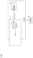
- FIG. 1 is a diagram illustrating a configuration example of an optical communication system according to an embodiment.
- FIG. 2 is a block diagram showing an outline of a configuration related to optical wavelength division multiplexing communication in an embodiment.
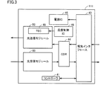
- FIG. 3 is a diagram showing a schematic configuration of an optical transceiver applicable to this embodiment.
- FIG. 4 is a block diagram schematically showing the configuration of the optical transmission module 50 shown in FIG.
- FIG. 5 is a schematic diagram for explaining a thermal connection between the laser diode, the submount, and the thermoelectric cooler shown in FIG.
- FIG. 6 is a diagram showing an example of the relationship between the drive current and the center wavelength of the laser beam for the laser diode (DFB-LD) applicable to this embodiment.
- FIG. 1 is a diagram illustrating a configuration example of an optical communication system according to an embodiment.
- FIG. 2 is a block diagram showing an outline of a configuration related to optical wavelength division multiplexing communication in an embodiment.
- FIG. 3 is a diagram showing a schematic configuration of
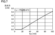
- FIG. 7 is a diagram showing an example of the relationship between drive current and optical output for a laser diode (EA-DFB-LD) applicable to this embodiment.
- FIG. 8 is a diagram showing an example of the relationship between the reverse bias voltage to the EA modulator and the DC extinction ratio for the laser diode (EA-DFB-LD) applicable to this embodiment.
- FIG. 9 is a block diagram illustrating a configuration example of a controller included in the optical transceiver.
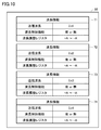
- FIG. 10 is a diagram illustrating an example of wavelength information.
- FIG. 11 is a flowchart for explaining the method of manufacturing the optical transmitter according to this embodiment.
- FIG. 12 is a schematic view showing one configuration example of the host substrate according to this embodiment.
- FIG. 13 is a schematic view showing another configuration example of the host substrate according to this embodiment.
- An object of the present disclosure is to suppress the influence of crosstalk noise due to four-wave mixing by an optical transmitter.
- An optical transmitter includes a plurality of light emitting units that transmit optical signals having different wavelengths. At least one light emitting unit among the plurality of light emitting units is configured to be capable of adjusting the wavelength.
- the influence of crosstalk noise due to four-wave mixing can be suppressed by the optical transmitter.
- at least one light emitting unit is configured to be capable of adjusting the wavelength of the optical signal. By adjusting the wavelength of the optical signal from the light emitting unit, the optical signal can be transmitted from each of the plurality of light emitting units so that the condition for generating the four-wave mixing distortion is not satisfied.
- the optical transmitter is provided in common to the plurality of light emitting units, and is thermocoupled to control the temperature of the plurality of light emitting units, and is thermally connected to the thermoelectric cooler.
- a plurality of thermal resistors thermally connected to each of the light emitting units, and a current supply unit configured to individually supply a driving current to the plurality of light emitting units.
- the plurality of light emitting portions are thermally separated from each other by the thermal resistance.
- the temperature of each light emitting unit can be controlled by a thermoelectric cooler and a thermal resistance. By changing the drive current supplied to the light emitting part whose wavelength can be adjusted, the temperature of the light emitting part can be changed. Thereby, the wavelength of the optical signal output from the light emission part can be adjusted.
- each of the plurality of thermal resistors is a submount on which the light emitting unit is mounted. According to the above, it is possible to change the temperature of the light emitting unit while eliminating the need for additional elements such as a heater.
- a well-known material is employable as a material of a submount.
- the current supply unit is configured to change the operating point of at least one light emitting unit capable of adjusting the wavelength upon receiving a control signal through the interface.
- the wavelength of the optical signal emitted from the light emitting unit whose wavelength can be adjusted can be changed. Thereby, the influence of four-wave mixing distortion can be suppressed.
- the optical transmitter further includes an interface for outputting wavelength information related to the wavelength of the optical signal to be output from at least one light emitting unit capable of adjusting the wavelength to the outside of the optical transmitter.
- information about the wavelength of the optical signal can be acquired from the optical transmitter through the interface. Thereby, for example, the presence or absence of the influence of four-wave mixing can be determined. Further, it is possible to eliminate the need to actually output light from the optical transmitter in order to measure the wavelength.
- the optical transmitter further includes a storage unit that stores an operating point of at least one light emitting unit capable of adjusting the wavelength.
- An optical transceiver includes the optical transmitter according to any one of (1) to (6) and an optical receiver.
- an optical transceiver capable of suppressing the influence of four-wave mixing distortion can be provided.
- An optical transmitter manufacturing method is an optical transmitter manufacturing method including a plurality of light emitting units that transmit optical signals having different wavelengths, and includes a plurality of light emitting units. At least one of the light emitting units is configured to be capable of adjusting the wavelength, and the manufacturing method sets the wavelength so that the wavelength of the optical signal output from the plurality of light emitting units deviates from the condition where the four-wave mixing distortion occurs.
- An optical transmitter includes a plurality of light emitting units that transmit optical signals having different wavelengths. At least one light emitting unit among the plurality of light emitting units is configured to be capable of adjusting the wavelength.
- the optical transmitter includes a storage unit that stores an operating point of at least one light-emitting unit capable of adjusting the wavelength so that the wavelengths of the optical signals output from the plurality of light-emitting units deviate from a condition in which four-wave mixing distortion occurs. Further prepare.
- FIG. 1 is a diagram illustrating a configuration example of an optical communication system according to an embodiment.
- a PON system 300 is an optical communication system according to an embodiment.
- the PON system 300 includes a station side device 301, a home side device 302, a PON line 303, and an optical splitter 304.
- the station side device (OLT (Optical Line Terminal)) 301 is installed in the station of a communication carrier.
- the station side device 301 mounts a host substrate (not shown).
- an optical transceiver (not shown) that converts electrical signals and optical signals into each other.
- a home-side device (ONU (Optical Network Unit)) 302 is installed on the user side.
- Each of the plurality of home side devices 302 is connected to the station side device 301 via the PON line 303.
- the PON line 303 is an optical communication line composed of an optical fiber.
- the PON line 303 includes a trunk optical fiber 305 and at least one branch optical fiber 306.
- the optical splitter 304 is connected to the trunk optical fiber 305 and the branch optical fiber 306.
- a plurality of home devices 302 can be connected to the PON line 303.
- the optical signal transmitted from the station side device 301 passes through the PON line 303 and is branched to a plurality of home side devices 302 by the optical splitter 304.
- the optical signal transmitted from each home apparatus 302 is focused by the optical splitter 304 and sent to the station apparatus 301 through the PON line 303.
- the optical splitter 304 passively branches or multiplexes the signal from the input signal without requiring any external power supply.
- a wavelength-multiplexed PON system in which a plurality of wavelengths are assigned to an upstream signal or a downstream signal and a plurality of wavelengths are wavelength-multiplexed to form an upstream signal or a downstream signal has been studied.
- an optical signal having a transmission capacity of 25.8 Gbps per wavelength is assigned to each of the upstream and the downstream in a wavelength-multiplexed manner.
- FIG. 2 is a block diagram showing an outline of a configuration related to optical wavelength division multiplexing communication in one embodiment.
- an optical transceiver 111 is mounted on the host substrate 1.
- the optical transceiver 111 is a 25.8 Gbps ⁇ 4 wavelength optical transceiver.
- the optical transceiver 111 includes a controller 41 that controls the operation of the optical transceiver 111.
- the host board 1 has an optical transceiver monitoring control block 20.
- the optical transceiver monitoring control block 20 can be realized by a semiconductor integrated circuit.
- the optical transceiver monitoring control block 20 can acquire information on at least one wavelength of the wavelength multiplexed light from the optical transceiver 111 through the management interface.
- the wavelength information is stored in the controller 41.
- the optical transceiver monitoring control block 20 can send a control signal to the controller 41 through the management interface.
- the controller 41 can adjust at least one wavelength of the wavelength multiplexed light output from the optical transceiver 111 according to the control signal.
- the optical transceiver monitoring control block 20 may detect an abnormality in the optical transceiver 111 based on information output from the optical transceiver 111. In this case, the optical transceiver monitoring control block 20 may notify the management device 200 of the occurrence of the abnormality. For example, when there is a possibility of the influence of crosstalk noise (four-wave mixing distortion) due to four-wave mixing, the optical transceiver monitoring control block 20 notifies the management apparatus 200.
- crosstalk noise four-wave mixing distortion
- FIG. 3 is a diagram showing a schematic configuration of an optical transceiver applicable to this embodiment.
- the optical transceiver 111 includes a controller 41, an electrical interface 43, a clock data recovery (CDR (Clock Data Recovery)) IC 44, a power supply IC 45, a temperature control IC 46, and an optical transmission module 50.
- the optical receiving module 60 realizes an optical receiver included in an optical transceiver.
- the controller 41 monitors and controls the optical transceiver 111.
- the controller 41 can store information related to the wavelength of wavelength multiplexed light output from the optical transceiver 111.
- a memory that stores information on the wavelength may be provided inside the optical transceiver 111 separately from the controller 41.
- the controller 41 may be integrated with another IC such as the temperature control IC 46.
- the electrical interface 43 inputs and outputs electrical signals.
- the optical transmission module 50 outputs data from the clock data recovery IC 44 in the form of an optical signal.
- the electrical interface 43 is an interface for outputting wavelength information from the inside of the optical transmitter to the outside of the optical transmitter.
- the electrical interface 43 is also an interface for receiving a control signal from the outside of the optical transmitter.
- the optical transmission module 50 is configured to change at least one operating point of the plurality of light emitting units (see FIG. 4) according to the control signal.
- the optical transmission module 50 includes a thermoelectric cooler (TEC) 48 that controls the temperature of a plurality of light emitting elements arranged in the optical transmission module 50.
- the thermoelectric cooler 48 can be realized by a Peltier element.
- the temperature control IC 46 sends a control signal to the thermoelectric cooler 48 in order to control the temperature of the thermoelectric cooler 48.
- one thermoelectric cooler (TEC) 48 is provided in common to the plurality of light emitting elements (laser diodes) in the optical transmission module 50.
- the optical receiving module 60 receives an optical signal and converts the optical signal into an electric signal.
- the electrical signal from the optical receiver module 60 is sent to the clock data recovery IC 44.
- the clock data recovery IC 44 is not limited to be built in the optical transceiver 111, and may be provided outside the optical transceiver 111 and on the host substrate 1.
- the clock data recovery IC on the transmission side and the clock data recovery IC on the reception side may be provided separately.
- Each IC may be incorporated in the optical transceiver 111 or provided outside the optical transceiver 111 and on the host substrate 1.
- FIG. 4 is a block diagram schematically showing the configuration of the optical transmission module 50 shown in FIG.
- the optical transmission module 50 includes a temperature monitor 10, laser diodes 11, 12, 13, 14, submounts 21, 22, 23, 24, a driver 30, and an optical wavelength multiplexer ( Optical MUX) 42 and a thermoelectric cooler 48.
- the optical transmission module 50 may be a TOSA (Transmitter Optical SubAssembly) type optical transmission module.
- the driver 30 supplies a drive current to each of the laser diodes 11, 12, 13, and 14 in response to a signal from the outside of the optical transmission module 50 (for example, the clock data recovery IC 44 shown in FIG. 3).
- Each of the laser diodes 11, 12, 13, and 14 outputs laser light when supplied with a current from the driver 30.
- the center wavelength of the laser light is different between the laser diodes 11, 12, 13, and 14.
- the laser diodes 11, 12, 13, and 14 serving as light emitting units can change the oscillation wavelength according to the supplied drive current.
- Examples of the laser diodes 11, 12, 13, and 14 include a distributed feedback laser diode (DFB-LD), an electroabsorption modulator integrated distributed feedback laser diode (EA-DFB-LD), or a semiconductor optical amplifier (SOA). SOA-integrated EA-DFB-LD in which are integrated).
- the optical wavelength multiplexer 42 multiplexes four optical signals having different wavelengths output from the laser diodes 11, 12, 13, and 14.
- the optical wavelength multiplexer 42 outputs optical signals having a plurality of wavelengths to an optical fiber (PON line) (not shown).
- the laser diodes 11, 12, 13, and 14 are mounted on the submounts 21, 22, 23, and 24, respectively.
- the submounts 21, 22, 23, and 24 are made of a material having a relatively high thermal conductivity.
- the submounts 21, 22, 23, 24 are made of aluminum nitride (AlN).
- the submounts 21, 22, 23, and 24 are in contact with the thermoelectric cooler 48. On the surface of the thermoelectric cooler 48, the submounts 21, 22, 23, 24 are arranged separately from each other.
- the temperature monitor 10 monitors the temperature of the surface of the thermoelectric cooler 48.
- FIG. 5 is a schematic diagram for explaining the thermal connection between the laser diode, the submount and the thermoelectric cooler shown in FIG. As shown in FIG. 5, each of the submounts 21, 22, 23, and 24 is thermally connected to a corresponding laser diode and thermally connected to a thermoelectric cooler 48. Each of the submounts 21, 22, 23, and 24 is an element having a thermal resistance. The laser diodes 11, 12, 13, and 14 are thermally separated from each other.
- the driver 30 (see FIG. 4) supplies drive currents I1, I2, I3, and I4 to the laser diodes 11, 12, 13, and 14, respectively.
- the driver 30 can individually adjust the drive currents I1, I2, I3, and I4. Thereby, the center wavelength of the laser beam output from each of the laser diodes 11, 12, 13, and 14 can be individually adjusted.
- at least one of the four laser diodes 11, 12, 13, and 14 may change the oscillation wavelength according to the drive current.
- the driver 30 and the submounts 21, 22, 23, and 24 are configured so that the wavelength of the optical signal can be individually adjusted for each light emitting unit (laser diode).
- FIG. 6 is a diagram showing an example of the relationship between the drive current and the center wavelength of the laser beam for the laser diode (DFB-LD) applicable to this embodiment.
- the relationship between the drive current and the center wavelength when the temperature Tld of the laser diode is 50 ° C. is shown.
- FIG. 6 shows an example of the range of the drive current I op that can be adjusted from the viewpoint of 25.8 Gbps characteristics and reliability assurance.
- the center wavelength can be changed from 1299.8 nm to 1300.0 nm within the range of the driving current I op from 32 mA to 46 mA.
- a driving current for outputting an optical signal having a desired wavelength is determined from the range of the driving current I op .
- FIG. 6 shows an example of the characteristics of any one of the laser diodes 11 to 14. Regarding the remaining laser diodes of the laser diodes 11 to 14, although the center wavelength is different, the center wavelength can be changed according to the drive current.
- the optical output power when the operating point is changed by changing the drive current, the optical output power also changes. For this reason, the optical output power may vary.
- the optical output is obtained by changing the drive current of the DFB-LD section. Even if the power increases, the light absorption amount of the EA modulator can be increased by changing the bias level of the EA modulator. Thereby, in the EA modulator, the optical output power can be corrected in the direction of reducing the optical output power. Note that the change in the bias level of the EA modulator does not contribute to the change in wavelength, but the optical waveform can change somewhat. Therefore, it is preferable to change the duty ratio of the modulation signal output of the driver 30.
- the wavelength can be adjusted by the current supplied to the DFB-LD unit, and the optical output power can be adjusted in the EA unit and the SOA unit. Can be adjusted. Therefore, in the embodiment in which the SOA integrated EA-DFB-LD is used for the laser diodes 11, 12, 13, and 14, more flexible adjustment can be realized, so that the wavelength adjustment range can be expanded.
- FIG. 9 is a block diagram showing a configuration example of a controller included in the optical transceiver.
- the controller 41 can include a storage unit 65.
- the storage unit 65 may be provided inside the optical transceiver separately from the controller 41.
- the storage unit 65 can store lane information 70 and wavelength information 71 to 74.
- the lane information 70 is information for associating four lanes (communication paths) of lane 1, lane 2, lane 3, and lane 4 with wavelengths ( ⁇ d1, ⁇ d2, ⁇ d3, ⁇ d4) of optical signals transmitted in each lane. is there.
- Transmission wavelengths ⁇ d1, ⁇ d2, ⁇ d3, and ⁇ d4 are wavelengths of optical signals transmitted from the laser diodes 11, 12, 13, and 14, respectively.
- the wavelength information 71 to 74 is information related to the transmission wavelengths ⁇ d1, ⁇ d2, ⁇ d3, and ⁇ d4, and corresponds to information on operating points of the laser diodes 11 to 14, respectively.
- FIG. 10 is a diagram showing an example of wavelength information.
- each of the wavelength information 71 to 74 includes transmission wavelength information ( ⁇ d1, ⁇ d2, ⁇ d3, ⁇ d4) and information indicating whether the wavelength control function is valid or invalid (for example, flag ), And a wavelength adjustment register.
- the wavelength adjustment register receives any value from + A to -A (A is a positive integer) and holds the value.
- the adjustment range of the transmission wavelength is determined by the value written in the wavelength adjustment register. For example, the transmission wavelength changes by 0.05 nm every time the register value is changed by one step.
- the value of the wavelength adjustment register is linked to the change in the temperature of the laser diode or the change in the drive current of the laser diode.
- the controller 41 can adjust the transmission wavelength specified by the wavelength information.
- the controller 41 determines the operating point of the corresponding laser diode among the laser diodes 11 to 14 based on the value written in the wavelength adjustment register.
- the controller 41 controls the drive current of the laser diode according to the operating point.
- the driver 30 controls the drive current of the laser diode.
- the controller 41 may further control the temperature of the thermoelectric cooler 48.
- the storage unit 65 only needs to store information on the wavelength to be changed among the wavelengths ⁇ d1, ⁇ d2, ⁇ d3, and ⁇ d4. Accordingly, the storage unit 65 stores at least one wavelength information.
- ITU-T G The specification of the zero dispersion wavelength of the single mode fiber indicated by 652 is defined as 1300 nm to 1324 nm.
- 63 nm) and ⁇ 4 1309.14 nm (1308.09 nm to 1310.19 nm).
- the zero-dispersion wavelength of the optical fiber matches the transmission wavelength and the phase matching condition between the wavelengths is satisfied. It is known that when the frequency of the input light is (fi, fj, fk), the frequency of the generated light is (fi + fj ⁇ fk). It is considered that the zero dispersion wavelength of the single mode fiber is distributed around 1312 nm near the center of the standard 1300 nm to 1324 nm. For this reason, in the wavelength arrangement of 100 GbE, the probability that the wavelength ⁇ 4 matches the zero dispersion wavelength of the optical fiber is the highest, and then the probability that the wavelength ⁇ 3 matches the zero dispersion wavelength of the optical fiber is high.
- the wavelength of the light generated by the four-wave mixing is the same as the wavelength of the signal light. For this reason, removal by the optical bandpass filter is impossible on the receiving side before O / E conversion. Therefore, reception characteristics on the receiving side are affected.
- the wavelength of light generated by four-wave mixing is very close to the wavelength of signal light, the light generated by four-wave mixing becomes coherent crosstalk noise.
- coherent crosstalk noise cannot be removed not only by the optical bandpass filter but also by the low-pass filter after O / E conversion. Therefore, coherent crosstalk noise is a factor that causes a large deterioration in reception characteristics.
- the wavelength ⁇ FWM that may enter the same wavelength region as the transmission wavelength region when four-wave mixing occurs is as follows.
- the wavelengths ⁇ d1, ⁇ d2, ⁇ d3, and ⁇ d4 of the four optical signals can be individually adjusted.
- the adjustment timing of the wavelengths ⁇ d1, ⁇ d2, ⁇ d3, and ⁇ d4 is not particularly limited.
- the wavelengths ⁇ d1, ⁇ d2, ⁇ d3, and ⁇ d4 of the four optical signals may be individually adjusted during the manufacturing stage.
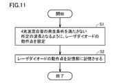
- FIG. 11 is a flowchart for explaining the method of manufacturing the optical transmitter according to this embodiment.
- the processing shown in this flowchart may be executed in the manufacturing stage of the optical transmitter, or may be executed in the stage of assembling the optical transceiver by combining the optical transmitter and the optical receiver.
- step S ⁇ b> 1 the laser diodes 11, 12, 13, and 14 are configured so that the wavelength of the optical signal output from the laser diode becomes a predetermined wavelength that does not affect the four-wave mixing distortion. Set the operating point. If the occurrence of four-wave mixing distortion can be avoided, at least one of the wavelengths ⁇ d1, ⁇ d2, ⁇ d3, and ⁇ d4 may be adjusted. Therefore, at least one of the operating points of the laser diodes 11, 12, 13, and 14 is adjusted as necessary.
- the optical transceiver monitoring control block 20 on the host substrate 1 may receive the values of the wavelengths ⁇ d1, ⁇ d2, ⁇ d3, and ⁇ d4, and determine whether these four wavelengths satisfy the condition for generating the four-wave mixing distortion. If the four-wave mixing distortion generation condition is satisfied, the determination process may be executed by changing at least one of the wavelengths ⁇ d1, ⁇ d2, ⁇ d3, and ⁇ d4.
- at least one adjustable wavelength is readjusted (finely adjusted) in consideration of wavelength combinations that reduce that possibility. )
- step S2 the operating point of the laser diode determined by the process in step S1 is stored in the storage unit 65. That is, the optical transmitter and the optical transceiver hold information on the operating point of the laser diode.
- the values of the drive currents I1, I2, I3, and I4 respectively associated with the wavelengths ⁇ d1, ⁇ d2, ⁇ d3, and ⁇ d4 determined by the process of step S1 may be stored in the storage unit 65.
- At least one value among the wavelengths ⁇ d1, ⁇ d2, ⁇ d3, and ⁇ d4 stored in the storage unit 65 may be changed when the optical transceiver 111 is used. Thereby, when the optical transceiver 111 is used, the wavelength of the optical signal can be adjusted so as not to cause the four-wave mixing distortion.
- the embodiment of the present invention includes a plurality of light emitting units (laser diodes 11 to 14) that transmit optical signals having different wavelengths, and at least one light emitting unit of the plurality of light emitting units includes The wavelength can be adjusted.
- an optical transmitter configured so as not to cause four-wave mixing distortion can be realized.
- it is possible to realize an optical transceiver including an optical transmitter that can reduce the possibility of four-wave mixing distortion.
- optical transmitter optical transceiver
- the possibility of four-wave mixing distortion can be reduced.
- a laser diode chip is designed and manufactured to emit light of a desired wavelength.
- the emission wavelength of the completed laser diode chip is not always as designed, and the emission wavelength may vary within a relatively wide range of specifications.
- the temperature from each laser diode can be controlled by the thermoelectric cooler 48 and the thermal resistance (corresponding submount of the submounts 21 to 24).
- the wavelength can be adjusted after the assembly of the optical transmitter so that the influence of the four-wave mixing distortion does not occur.
- the optical transmitter can store the adjusted wavelength information.
- information on the wavelength of the optical signal can be acquired from the optical transmitter through the interface. If the optical transmitter does not have wavelength information, it is necessary to actually output light from the optical transmitter and measure the wavelength in order to obtain wavelength information. According to the embodiment of the present invention, it is possible to acquire information about the wavelength of an optical signal while making it unnecessary to actually output light from an optical transmitter.
- the embodiment of the present invention can be applied to an optical transmission system including a light emitting unit that outputs a plurality of optical signals having different wavelengths. Therefore, as illustrated below, in this embodiment, the optical transceiver is not limited to a four-wavelength optical transceiver. Further, it is not limited to acquiring at least three wavelength information from one optical transceiver, and information on at least three wavelengths may be acquired from a plurality of optical transceivers.
- FIG. 12 is a schematic view showing one configuration example of the host substrate according to this embodiment.
- the optical transceivers 112 and 111 a are mounted on the host substrate 1.
- the optical transceiver 111a is a three-wavelength optical transceiver, and outputs optical signals having wavelengths ⁇ 2, ⁇ 3, and ⁇ 4.
- the optical transceiver 112 outputs an optical signal having a wavelength ⁇ 1.
- the optical wavelength multiplexer receives an optical signal from each of the optical transceivers 112 and 111a and generates a wavelength multiplexed optical signal.
- the three wavelengths of the optical transceiver 111a may be any three of the wavelengths ⁇ 1, ⁇ 2, ⁇ 3, and ⁇ 4.
- the optical transceiver monitoring control block 20 reads information indicating the wavelengths ⁇ 2, ⁇ 3, and ⁇ 4 from the controller 51 of the optical transceiver 112 through the management interface.
- the optical transceiver monitoring control block 20 may read information indicating the wavelength ⁇ 1 from the controller 41 of the optical transceiver 111a through the management interface.
- wavelength information is sent from the optical transceiver to the optical transceiver monitoring control block 20. Since the configuration of controllers 41 and 51 is the same as the configuration shown in FIG. 9, the following description will not be repeated.
- the optical transceiver monitoring control block 20 determines the presence or absence of the influence of the four-wave mixing distortion based on the wavelength information from the optical transceivers 112 and 111a. When there is an influence of four-wave mixing distortion, the optical transceiver monitoring control block 20 sends a control signal to the controller 51 of the optical transceiver 112 to adjust the wavelengths ⁇ 2, ⁇ 3, and ⁇ 4.
- FIG. 13 is a schematic view showing another configuration example of the host substrate according to this embodiment.
- the optical transceivers 113 a and 113 b are mounted on the host substrate 1.
- Each of the optical transceivers 113a and 113b is a two-wavelength optical transceiver.
- the optical transceiver 113a outputs optical signals having wavelengths ⁇ 1 and ⁇ 2.
- the optical transceiver 113b outputs an optical signal having wavelengths ⁇ 3 and ⁇ 4.
- the combination of the two wavelengths of the optical transceivers 113a and 113b is not limited.
- the optical transceiver monitoring control block 20 reads the wavelength information indicating the wavelengths ⁇ 1 and ⁇ 2 from the controller 41a of the optical transceiver 113a through the management interface. Similarly, the optical transceiver monitoring control block 20 reads wavelength information indicating the wavelengths ⁇ 3 and ⁇ 4 from the controller 41b of the optical transceiver 113b through the management interface. Since the configuration of controllers 41a and 41b is the same as the configuration shown in FIG. 9, the following description will not be repeated.
- the optical transceiver monitoring control block 20 determines whether or not there is an influence of the four-wave mixing distortion based on the wavelength information from the optical transceivers 113a and 113b. When there is an influence of four-wave mixing distortion, the optical transceiver monitoring control block 20 sends a control signal to the controllers 41a and 41b to adjust the wavelengths ⁇ 2, ⁇ 3, and ⁇ 4.
Abstract
This optical transmitter is provided with multiple light emitting units which transmit optical signals having mutually different wavelengths and are configured to have a modifiable optical signal wavelength. At least one of the light emitting units is configured to have an adjustable wavelength.
Description
本発明は、光送信器、光トランシーバおよび光送信器の製造方法に関する。本出願は、2016年12月28日に出願した日本特許出願である特願2016-256477号に基づく優先権を主張する。当該日本特許出願に記載された全ての記載内容は、参照によって本明細書に援用される。
The present invention relates to an optical transmitter, an optical transceiver, and an optical transmitter manufacturing method. This application claims priority based on Japanese Patent Application No. 2016-256477, which is a Japanese patent application filed on December 28, 2016. All the descriptions described in the Japanese patent application are incorporated herein by reference.
光通信における伝送容量は飛躍的に高められている。近年では、100Gbpsの伝送容量を有する光通信が提案されている。
The transmission capacity in optical communication has been dramatically increased. In recent years, optical communication having a transmission capacity of 100 Gbps has been proposed.
たとえば、100ギガビットイーサネット(注:イーサネットは登録商標)あるいは100G-EPON(Ethernet(登録商標) Passive Optical Network)では、速度25.8Gbpsの互いに波長が異なる4本の光信号が送信される。具体的には、これら4本の光信号は波長分割多重(WDM)方式に従って多重化される。波長多重光は、光ファイバを通して伝送される。
For example, in 100 Gigabit Ethernet (Note: Ethernet is a registered trademark) or 100G-EPON (Ethernet (registered trademark) Passive Optical Network), four optical signals having different wavelengths and having a speed of 25.8 Gbps are transmitted. Specifically, these four optical signals are multiplexed according to a wavelength division multiplexing (WDM) system. Wavelength multiplexed light is transmitted through an optical fiber.
光ファイバのゼロ分散波長と波長多重信号の複数の波長とが、所定の条件を満たす場合に、その光ファイバの内部において4光波混合が生じる。4光波混合によって発生した光は、複数のチャネルのうちのあるチャネルの光信号に重畳することによって、クロストークノイズを誘発する。このために通信品質の劣化という問題が起こり得る。光信号の長距離の伝送のために光信号(波長多重光)のパワーを大きくするほど、4光波混合による信号の歪が大きくなる。
When the zero dispersion wavelength of the optical fiber and the plurality of wavelengths of the wavelength multiplexed signal satisfy a predetermined condition, four-wave mixing occurs inside the optical fiber. Light generated by the four-wave mixing induces crosstalk noise by being superimposed on an optical signal of a certain channel among a plurality of channels. For this reason, the problem of deterioration of communication quality may occur. As the power of the optical signal (wavelength multiplexed light) is increased for long-distance transmission of the optical signal, the distortion of the signal due to four-wave mixing increases.
特開2007-5484号公報(特許文献1)は、4光波混合の低減に向けられた光増幅装置を開示する。この光増幅装置は、信号帯域で正の波長分散を持ち、かつ波長多重化信号を増幅する光ファイバと、その光ファイバに励起光を入射する励起部とを有する。
Japanese Patent Laid-Open No. 2007-5484 (Patent Document 1) discloses an optical amplifying device directed to reducing four-wave mixing. This optical amplifying device has an optical fiber that has positive chromatic dispersion in a signal band and amplifies a wavelength multiplexed signal, and a pumping unit that makes pumping light incident on the optical fiber.
小林 亘、外5名、「SOA集積EADFBレーザによる消費電力削減と伝送距離延伸」、信学技報、電気情報通信学会、2015年10月、OSC2015-78(非特許文献1)は、SOA(半導体光増幅器)が集積されたEADFBレーザ(電界吸収型変調器集積分布帰還型レーザ)によって、従来のEADFBレーザに比べて消費電力の低減および光出力の増加が可能であることを報告する。
Wataru Kobayashi, 5 others, “Power consumption reduction and transmission distance extension by SOA integrated EADFB laser”, IEICE Technical Report, IEICE, October 2015, OSC2015-78 (Non-patent Document 1) We report that EADFB laser (electroabsorption modulator integrated distributed feedback laser) integrated with a semiconductor optical amplifier can reduce power consumption and increase optical output as compared with a conventional EADFB laser.
本発明の一態様に係る光送信器は、互いに異なる波長を有する光信号を送出し、かつ光信号の波長を変更可能に構成された、複数の発光部と、光信号の波長を発光部ごとに個別に調整可能に構成された波長調整部とを備える。
An optical transmitter according to an aspect of the present invention is configured to transmit an optical signal having a wavelength different from each other and to change the wavelength of the optical signal, and to change the wavelength of the optical signal for each light emitting unit. And a wavelength adjusting unit configured to be individually adjustable.
[本開示が解決しようとする課題]
本開示の目的は、4光波混合によるクロストークノイズの影響を、光送信器によって抑制することである。 [Problems to be solved by this disclosure]
An object of the present disclosure is to suppress the influence of crosstalk noise due to four-wave mixing by an optical transmitter.
本開示の目的は、4光波混合によるクロストークノイズの影響を、光送信器によって抑制することである。 [Problems to be solved by this disclosure]
An object of the present disclosure is to suppress the influence of crosstalk noise due to four-wave mixing by an optical transmitter.
[本発明の実施形態の説明]
最初に本発明の実施態様を列記して説明する。 [Description of Embodiment of the Present Invention]
First, embodiments of the present invention will be listed and described.
最初に本発明の実施態様を列記して説明する。 [Description of Embodiment of the Present Invention]
First, embodiments of the present invention will be listed and described.
(1)本発明の一態様に係る光送信器は、互いに異なる波長を有する光信号を送出する複数の発光部を備える。複数の発光部のうちの少なくとも1つの発光部は、波長を調整可能に構成される。
(1) An optical transmitter according to an aspect of the present invention includes a plurality of light emitting units that transmit optical signals having different wavelengths. At least one light emitting unit among the plurality of light emitting units is configured to be capable of adjusting the wavelength.
上記によれば、4光波混合によるクロストークノイズの影響を、光送信器によって抑制することができる。複数の発光部のうち、少なくとも1つの発光部は、光信号の波長を調整可能に構成される。その発光部からの光信号の波長を調整することによって、4光波混合歪みが発生する条件が成立しないように、複数の発光部の各々から光信号を送出することができる。
According to the above, the influence of crosstalk noise due to four-wave mixing can be suppressed by the optical transmitter. Among the plurality of light emitting units, at least one light emitting unit is configured to be capable of adjusting the wavelength of the optical signal. By adjusting the wavelength of the optical signal from the light emitting unit, the optical signal can be transmitted from each of the plurality of light emitting units so that the condition for generating the four-wave mixing distortion is not satisfied.
(2)好ましくは、光送信器は、複数の発光部に対して共通に設けられて、複数の発光部の温度を制御する熱電クーラと、熱電クーラに熱的に接続されるとともに、複数の発光部のそれぞれに熱的に接続される複数の熱抵抗と、複数の発光部に個別に駆動電流を供給するように構成された電流供給部とをさらに備える。
(2) Preferably, the optical transmitter is provided in common to the plurality of light emitting units, and is thermocoupled to control the temperature of the plurality of light emitting units, and is thermally connected to the thermoelectric cooler. A plurality of thermal resistors thermally connected to each of the light emitting units, and a current supply unit configured to individually supply a driving current to the plurality of light emitting units.
上記によれば、複数の発光部は、熱抵抗によって互いに熱的に分離される。各発光部の温度は、熱電クーラおよび熱抵抗によって制御可能である。波長を調整可能な発光部に供給される駆動電流を変化させることによって、その発光部の温度を変化させることができる。これにより、その発光部から出力される光信号の波長を調整することができる。
According to the above, the plurality of light emitting portions are thermally separated from each other by the thermal resistance. The temperature of each light emitting unit can be controlled by a thermoelectric cooler and a thermal resistance. By changing the drive current supplied to the light emitting part whose wavelength can be adjusted, the temperature of the light emitting part can be changed. Thereby, the wavelength of the optical signal output from the light emission part can be adjusted.
(3)好ましくは、複数の熱抵抗の各々は、発光部が実装されるサブマウントである。
上記によれば、ヒータ等の追加の素子を不要としながら発光部の温度を変化させることができる。なお、サブマウントの材料として公知の材料を採用することができる。 (3) Preferably, each of the plurality of thermal resistors is a submount on which the light emitting unit is mounted.
According to the above, it is possible to change the temperature of the light emitting unit while eliminating the need for additional elements such as a heater. In addition, a well-known material is employable as a material of a submount.
(4)好ましくは、電流供給部は、インタフェースを通じて制御信号を受けて、波長を調整可能な少なくとも1つの発光部の動作点を変化させるように構成される。
(4) Preferably, the current supply unit is configured to change the operating point of at least one light emitting unit capable of adjusting the wavelength upon receiving a control signal through the interface.
上記によれば、動作点を変化させることによって、波長を調整可能な発光部から出る光信号の波長を変化させることができる。これにより4光波混合歪みの影響を抑制することができる。
According to the above, by changing the operating point, the wavelength of the optical signal emitted from the light emitting unit whose wavelength can be adjusted can be changed. Thereby, the influence of four-wave mixing distortion can be suppressed.
(5)好ましくは、光送信器は、波長を調整可能な少なくとも1つの発光部から出力されるべき光信号の波長に関する波長情報を、光送信器の外部に出力するためのインタフェースをさらに備える。
(5) Preferably, the optical transmitter further includes an interface for outputting wavelength information related to the wavelength of the optical signal to be output from at least one light emitting unit capable of adjusting the wavelength to the outside of the optical transmitter.
上記によれば、インタフェースを通じて、光信号の波長についての情報を光送信器から取得することができる。これにより、たとえば4光波混合の影響の有無を判断することができる。また、波長を測定するために光送信器から実際に光を出力することを不要にすることができる。
According to the above, information about the wavelength of the optical signal can be acquired from the optical transmitter through the interface. Thereby, for example, the presence or absence of the influence of four-wave mixing can be determined. Further, it is possible to eliminate the need to actually output light from the optical transmitter in order to measure the wavelength.
(6)好ましくは、光送信器は、波長を調整可能な少なくとも1つの発光部の動作点を記憶する記憶部をさらに備える。
(6) Preferably, the optical transmitter further includes a storage unit that stores an operating point of at least one light emitting unit capable of adjusting the wavelength.
上記によれば、記憶された動作点に従って、波長を調整可能な少なくとも1つの発光部を制御することができる。したがって、4光波混合歪みの影響を抑制することができる。
According to the above, it is possible to control at least one light emitting unit capable of adjusting the wavelength in accordance with the stored operating point. Therefore, the influence of four-wave mixing distortion can be suppressed.
(7)本発明の一態様に係る光トランシーバは、(1)から(6)のいずれかに記載の光送信器と、光受信器とを備える。
(7) An optical transceiver according to an aspect of the present invention includes the optical transmitter according to any one of (1) to (6) and an optical receiver.
上記によれば、4光波混合歪みの影響を抑制可能な光トランシーバを提供することができる。
According to the above, an optical transceiver capable of suppressing the influence of four-wave mixing distortion can be provided.
(8)本発明の一態様に係る光送信器の製造方法は、互いに異なる波長を有する光信号を送出する複数の発光部を備えた光送信器の製造方法であって、複数の発光部のうちの少なくとも1つの発光部は、波長を調整可能に構成され、製造方法は、複数の発光部から出力される光信号の波長が、4光波混合歪みの発生する条件から外れるように、波長を調整可能な少なくとも1つの発光部の動作点を設定する工程と、設定する工程において設定された動作点を、光送信器に記憶させる工程とを備える。
(8) An optical transmitter manufacturing method according to an aspect of the present invention is an optical transmitter manufacturing method including a plurality of light emitting units that transmit optical signals having different wavelengths, and includes a plurality of light emitting units. At least one of the light emitting units is configured to be capable of adjusting the wavelength, and the manufacturing method sets the wavelength so that the wavelength of the optical signal output from the plurality of light emitting units deviates from the condition where the four-wave mixing distortion occurs. A step of setting an operating point of at least one light-emitting unit that can be adjusted, and a step of storing the operating point set in the setting step in an optical transmitter.
上記によれば、4光波混合歪みの影響を抑制可能な光送信器を製造できる。
(9)本発明の一態様に係る光送信器は、互いに異なる波長を有する光信号を送出する複数の発光部を備える。複数の発光部のうちの少なくとも1つの発光部は、波長を調整可能に構成される。光送信器は、複数の発光部から出力される光信号の波長が4光波混合歪みの発生する条件から外れるための、波長を調整可能な少なくとも1つの発光部の動作点を記憶する記憶部をさらに備える。 Based on the above, it is possible to manufacture an optical transmitter capable of suppressing the influence of four-wave mixing distortion.
(9) An optical transmitter according to an aspect of the present invention includes a plurality of light emitting units that transmit optical signals having different wavelengths. At least one light emitting unit among the plurality of light emitting units is configured to be capable of adjusting the wavelength. The optical transmitter includes a storage unit that stores an operating point of at least one light-emitting unit capable of adjusting the wavelength so that the wavelengths of the optical signals output from the plurality of light-emitting units deviate from a condition in which four-wave mixing distortion occurs. Further prepare.
上記によれば、4光波混合歪みの影響を抑制可能な光送信器を製造できる。
[本発明の実施形態の詳細]
以下、本発明の実施の形態について図面を用いて説明する。なお、図中同一または相当部分には同一符号を付してその説明は繰り返さない。 Based on the above, it is possible to manufacture an optical transmitter capable of suppressing the influence of four-wave mixing distortion.
[Details of the embodiment of the present invention]
Hereinafter, embodiments of the present invention will be described with reference to the drawings. In the drawings, the same or corresponding parts are denoted by the same reference numerals and description thereof will not be repeated.
図1は、一実施形態に係る光通信システムの構成例を示した図である。図1において、PONシステム300は、一実施形態に係る光通信システムである。PONシステム300は、局側装置301と、宅側装置302と、PON回線303と、光スプリッタ304とを備える。
FIG. 1 is a diagram illustrating a configuration example of an optical communication system according to an embodiment. In FIG. 1, a PON system 300 is an optical communication system according to an embodiment. The PON system 300 includes a station side device 301, a home side device 302, a PON line 303, and an optical splitter 304.
局側装置(OLT(Optical Line Terminal))301は、通信事業者の局舎に設置される。局側装置301は、ホスト基板(図示せず)を搭載する。ホスト基板には、電気信号と光信号とを相互に変換する光トランシーバ(図示せず)が接続される。
The station side device (OLT (Optical Line Terminal)) 301 is installed in the station of a communication carrier. The station side device 301 mounts a host substrate (not shown). Connected to the host substrate is an optical transceiver (not shown) that converts electrical signals and optical signals into each other.
宅側装置(ONU(Optical Network Unit))302は、ユーザ側に設置される。複数の宅側装置302の各々は、PON回線303を介して局側装置301に接続される。
A home-side device (ONU (Optical Network Unit)) 302 is installed on the user side. Each of the plurality of home side devices 302 is connected to the station side device 301 via the PON line 303.
PON回線303は、光ファイバにより構成された光通信回線である。PON回線303は、幹線光ファイバ305、および、少なくとも1つの支線光ファイバ306を含む。光スプリッタ304は、幹線光ファイバ305および支線光ファイバ306に接続される。PON回線303には、複数の宅側装置302が接続可能である。
The PON line 303 is an optical communication line composed of an optical fiber. The PON line 303 includes a trunk optical fiber 305 and at least one branch optical fiber 306. The optical splitter 304 is connected to the trunk optical fiber 305 and the branch optical fiber 306. A plurality of home devices 302 can be connected to the PON line 303.
局側装置301から送信された光信号は、PON回線303を通り、光スプリッタ304によって複数の宅側装置302へと分岐される。一方、各々の宅側装置302から送信された光信号は、光スプリッタ304によって集束されるとともに、PON回線303を通って局側装置301に送られる。光スプリッタ304は、外部からの電源供給を特に必要とすることなく、入力された信号から受動的に信号を分岐または多重する。
The optical signal transmitted from the station side device 301 passes through the PON line 303 and is branched to a plurality of home side devices 302 by the optical splitter 304. On the other hand, the optical signal transmitted from each home apparatus 302 is focused by the optical splitter 304 and sent to the station apparatus 301 through the PON line 303. The optical splitter 304 passively branches or multiplexes the signal from the input signal without requiring any external power supply.
高速PONシステムとして、上り信号または下り信号に複数波長が割り当てられ、複数波長を波長多重して上り信号または下り信号を構成する波長多重型PONシステムが検討されている。たとえば100Gbps級PONでは、上りおよび下りに、1波長あたりの伝送容量が25.8Gbpsの光信号をそれぞれ4波長割り当て、それらを波長多重する構成とすることができる。
As a high-speed PON system, a wavelength-multiplexed PON system in which a plurality of wavelengths are assigned to an upstream signal or a downstream signal and a plurality of wavelengths are wavelength-multiplexed to form an upstream signal or a downstream signal has been studied. For example, in a 100 Gbps class PON, an optical signal having a transmission capacity of 25.8 Gbps per wavelength is assigned to each of the upstream and the downstream in a wavelength-multiplexed manner.
図2は、一実施形態における、光波長多重通信に関する構成の概略を示したブロック図である。図2を参照して、光トランシーバ111が、ホスト基板1に実装される。光トランシーバ111は、25.8Gbps×4波長光トランシーバである。光トランシーバ111は、光トランシーバ111の動作を制御するコントローラ41を含む。
FIG. 2 is a block diagram showing an outline of a configuration related to optical wavelength division multiplexing communication in one embodiment. With reference to FIG. 2, an optical transceiver 111 is mounted on the host substrate 1. The optical transceiver 111 is a 25.8 Gbps × 4 wavelength optical transceiver. The optical transceiver 111 includes a controller 41 that controls the operation of the optical transceiver 111.
ホスト基板1は、光トランシーバ監視制御ブロック20を有する。光トランシーバ監視制御ブロック20は、半導体集積回路により実現可能である。光トランシーバ監視制御ブロック20は、マネージメントインタフェースを通じて、光トランシーバ111から波長多重光の少なくとも1つの波長に関する情報を取得することができる。波長情報はコントローラ41の内部に記憶される。
The host board 1 has an optical transceiver monitoring control block 20. The optical transceiver monitoring control block 20 can be realized by a semiconductor integrated circuit. The optical transceiver monitoring control block 20 can acquire information on at least one wavelength of the wavelength multiplexed light from the optical transceiver 111 through the management interface. The wavelength information is stored in the controller 41.
光トランシーバ監視制御ブロック20は、マネージメントインタフェースを通じて、コントローラ41に制御信号を送ることができる。コントローラ41は、制御信号に応じて、光トランシーバ111から出力される波長多重光の少なくとも1つの波長を調整することができる。光トランシーバ監視制御ブロック20は、光トランシーバ111から出力される情報に基づいて、光トランシーバ111の異常を検出してもよい。この場合、光トランシーバ監視制御ブロック20は、管理装置200にその異常の発生を通知してもよい。たとえば4光波混合によるクロストークノイズ(4光波混合歪み)の影響が生じる可能性がある場合は、光トランシーバ監視制御ブロック20は、管理装置200に通知する。
The optical transceiver monitoring control block 20 can send a control signal to the controller 41 through the management interface. The controller 41 can adjust at least one wavelength of the wavelength multiplexed light output from the optical transceiver 111 according to the control signal. The optical transceiver monitoring control block 20 may detect an abnormality in the optical transceiver 111 based on information output from the optical transceiver 111. In this case, the optical transceiver monitoring control block 20 may notify the management device 200 of the occurrence of the abnormality. For example, when there is a possibility of the influence of crosstalk noise (four-wave mixing distortion) due to four-wave mixing, the optical transceiver monitoring control block 20 notifies the management apparatus 200.
図3は、この実施の形態に適用可能な光トランシーバの概略的な構成を示した図である。図3に示されるように、光トランシーバ111は、コントローラ41と、電気インタフェース43と、クロックデータ再生(CDR(Clock Data Recovery))IC44と、電源IC45と、温度制御IC46と、光送信モジュール50と、光受信モジュール60とを含む。この実施の形態において、光受信モジュール60は、光トランシーバに含まれる光受信器を実現する。
FIG. 3 is a diagram showing a schematic configuration of an optical transceiver applicable to this embodiment. As shown in FIG. 3, the optical transceiver 111 includes a controller 41, an electrical interface 43, a clock data recovery (CDR (Clock Data Recovery)) IC 44, a power supply IC 45, a temperature control IC 46, and an optical transmission module 50. And the optical receiving module 60. In this embodiment, the optical receiver module 60 realizes an optical receiver included in an optical transceiver.
コントローラ41は、光トランシーバ111を監視および制御する。コントローラ41は、光トランシーバ111から出力される波長多重光の波長に関する情報を記憶することができる。波長に関する情報を記憶するメモリが、コントローラ41とは別に光トランシーバ111の内部に設けられてもよい。コントローラ41は、温度制御IC46などの他のICと統合されていてもよい。
The controller 41 monitors and controls the optical transceiver 111. The controller 41 can store information related to the wavelength of wavelength multiplexed light output from the optical transceiver 111. A memory that stores information on the wavelength may be provided inside the optical transceiver 111 separately from the controller 41. The controller 41 may be integrated with another IC such as the temperature control IC 46.
電気インタフェース43は、電気信号を入力および出力する。光送信モジュール50は、クロックデータ再生IC44からのデータを光信号の形態で出力する。電気インタフェース43は、波長情報を光送信器の内部から光送信器の外部に出力するためのインタフェースである。電気インタフェース43は、光送信器の外部から制御信号を受けるためのインタフェースでもある。光送信モジュール50は、制御信号に応じて、複数の発光部(図4を参照)のうちの少なくとも1つの動作点を変化させるように構成される。
The electrical interface 43 inputs and outputs electrical signals. The optical transmission module 50 outputs data from the clock data recovery IC 44 in the form of an optical signal. The electrical interface 43 is an interface for outputting wavelength information from the inside of the optical transmitter to the outside of the optical transmitter. The electrical interface 43 is also an interface for receiving a control signal from the outside of the optical transmitter. The optical transmission module 50 is configured to change at least one operating point of the plurality of light emitting units (see FIG. 4) according to the control signal.
光送信モジュール50は、光送信モジュール50内に配置された複数の発光素子の温度を制御する熱電クーラ(TEC)48を含む。熱電クーラ48は、ペルチェ素子によって実現可能である。温度制御IC46は、熱電クーラ48の温度を制御するために熱電クーラ48に制御信号を送る。後述するように、光送信モジュール50の内部には、1つの熱電クーラ(TEC)48が複数の発光素子(レーザダイオード)に対して共通して設けられる。
The optical transmission module 50 includes a thermoelectric cooler (TEC) 48 that controls the temperature of a plurality of light emitting elements arranged in the optical transmission module 50. The thermoelectric cooler 48 can be realized by a Peltier element. The temperature control IC 46 sends a control signal to the thermoelectric cooler 48 in order to control the temperature of the thermoelectric cooler 48. As will be described later, one thermoelectric cooler (TEC) 48 is provided in common to the plurality of light emitting elements (laser diodes) in the optical transmission module 50.
光受信モジュール60は、光信号を受信して、その光信号を電気信号に変換する。光受信モジュール60からの電気信号は、クロックデータ再生IC44へと送られる。クロックデータ再生IC44は、光トランシーバ111に内蔵されるよう限定されず、光トランシーバ111の外部、かつホスト基板1上に設けられてもよい。
The optical receiving module 60 receives an optical signal and converts the optical signal into an electric signal. The electrical signal from the optical receiver module 60 is sent to the clock data recovery IC 44. The clock data recovery IC 44 is not limited to be built in the optical transceiver 111, and may be provided outside the optical transceiver 111 and on the host substrate 1.
送信側のクロックデータ再生ICと受信側のクロックデータ再生ICとは個別に設けられてもよい。それぞれのICは、光トランシーバ111に内蔵されてもよく、光トランシーバ111の外部、かつホスト基板1上に設けられてもよい。
The clock data recovery IC on the transmission side and the clock data recovery IC on the reception side may be provided separately. Each IC may be incorporated in the optical transceiver 111 or provided outside the optical transceiver 111 and on the host substrate 1.
図4は、図3に示された光送信モジュール50の構成を概略的に示したブロック図である。図4に示されるように、光送信モジュール50は、温度モニタ10と、レーザダイオード11,12,13,14と、サブマウント21,22,23,24と、ドライバ30と、光波長多重器(光MUX)42と、熱電クーラ48とを備える。光送信モジュール50は、TOSA(Transmitter Optical SubAssembly)型の光送信モジュールであってもよい。
FIG. 4 is a block diagram schematically showing the configuration of the optical transmission module 50 shown in FIG. As shown in FIG. 4, the optical transmission module 50 includes a temperature monitor 10, laser diodes 11, 12, 13, 14, submounts 21, 22, 23, 24, a driver 30, and an optical wavelength multiplexer ( Optical MUX) 42 and a thermoelectric cooler 48. The optical transmission module 50 may be a TOSA (Transmitter Optical SubAssembly) type optical transmission module.
ドライバ30は、光送信モジュール50の外部(たとえば図3に示されたクロックデータ再生IC44)からの信号に応答して、レーザダイオード11,12,13,14の各々に駆動電流を供給する。レーザダイオード11,12,13,14の各々は、ドライバ30から電流が供給されることにより、レーザ光を出力する。レーザ光の中心波長は、レーザダイオード11,12,13,14の間で互いに異なる。
The driver 30 supplies a drive current to each of the laser diodes 11, 12, 13, and 14 in response to a signal from the outside of the optical transmission module 50 (for example, the clock data recovery IC 44 shown in FIG. 3). Each of the laser diodes 11, 12, 13, and 14 outputs laser light when supplied with a current from the driver 30. The center wavelength of the laser light is different between the laser diodes 11, 12, 13, and 14.
発光部としてのレーザダイオード11,12,13,14は、各々供給される駆動電流に応じて発振波長を変化させることができる。レーザダイオード11,12,13,14には、たとえば分布帰還型レーザダイオード(DFB-LD)あるいは、電界吸収型変調器集積分布帰還型レーザダイオード(EA-DFB-LD)あるいは、半導体光増幅器(SOA)が集積されたSOA集積EA-DFB-LDを用いることができる。
The laser diodes 11, 12, 13, and 14 serving as light emitting units can change the oscillation wavelength according to the supplied drive current. Examples of the laser diodes 11, 12, 13, and 14 include a distributed feedback laser diode (DFB-LD), an electroabsorption modulator integrated distributed feedback laser diode (EA-DFB-LD), or a semiconductor optical amplifier (SOA). SOA-integrated EA-DFB-LD in which are integrated).
光波長多重器42は、レーザダイオード11,12,13,14から出力された、異なる波長を有する4つの光信号を合波する。光波長多重器42は、複数の波長を有する光信号を、図示しない光ファイバ(PON回線)へと出力する。
The optical wavelength multiplexer 42 multiplexes four optical signals having different wavelengths output from the laser diodes 11, 12, 13, and 14. The optical wavelength multiplexer 42 outputs optical signals having a plurality of wavelengths to an optical fiber (PON line) (not shown).
レーザダイオード11,12,13,14は、サブマウント21,22,23,24にそれぞれ実装される。サブマウント21,22,23,24は、比較的高い熱伝導率を有する材料からなる。一実施形態では、サブマウント21,22,23,24は、窒化アルミニウム(AlN)からなる。
The laser diodes 11, 12, 13, and 14 are mounted on the submounts 21, 22, 23, and 24, respectively. The submounts 21, 22, 23, and 24 are made of a material having a relatively high thermal conductivity. In one embodiment, the submounts 21, 22, 23, 24 are made of aluminum nitride (AlN).
サブマウント21,22,23,24は熱電クーラ48に接触している。熱電クーラ48の表面において、サブマウント21,22,23,24は、互いに分離されて配置される。温度モニタ10は、熱電クーラ48の表面の温度をモニタする。
The submounts 21, 22, 23, and 24 are in contact with the thermoelectric cooler 48. On the surface of the thermoelectric cooler 48, the submounts 21, 22, 23, 24 are arranged separately from each other. The temperature monitor 10 monitors the temperature of the surface of the thermoelectric cooler 48.
図5は、図4に示されたレーザダイオード、サブマウントおよび熱電クーラの間の熱的な接続を説明するための模式図である。図5に示されるように、サブマウント21,22,23,24の各々は、対応するレーザダイオードに熱的に接続されるとともに、熱電クーラ48に熱的に接続される。サブマウント21,22,23,24の各々は、熱抵抗を有する素子である。レーザダイオード11,12,13,14は、互いに熱的に分離されている。
FIG. 5 is a schematic diagram for explaining the thermal connection between the laser diode, the submount and the thermoelectric cooler shown in FIG. As shown in FIG. 5, each of the submounts 21, 22, 23, and 24 is thermally connected to a corresponding laser diode and thermally connected to a thermoelectric cooler 48. Each of the submounts 21, 22, 23, and 24 is an element having a thermal resistance. The laser diodes 11, 12, 13, and 14 are thermally separated from each other.
ドライバ30(図4参照)は、レーザダイオード11,12,13,14にそれぞれ駆動電流I1,I2,I3,I4を供給する。ドライバ30は、駆動電流I1,I2,I3,I4を個別に調整することができる。これによりレーザダイオード11,12,13,14の各々から出力されるレーザ光の中心波長を個別に調整することができる。なお、波長の調整の際には、4つのレーザダイオード11,12,13,14のうち少なくとも1つが駆動電流に応じて発振波長を変化させるのでもよい。
The driver 30 (see FIG. 4) supplies drive currents I1, I2, I3, and I4 to the laser diodes 11, 12, 13, and 14, respectively. The driver 30 can individually adjust the drive currents I1, I2, I3, and I4. Thereby, the center wavelength of the laser beam output from each of the laser diodes 11, 12, 13, and 14 can be individually adjusted. When adjusting the wavelength, at least one of the four laser diodes 11, 12, 13, and 14 may change the oscillation wavelength according to the drive current.
波長を調整するために、駆動電流を調整するだけでなく、熱電クーラ48の温度も調整してもよい。この実施の形態において、ドライバ30およびサブマウント21,22,23,24は、光信号の波長を発光部(レーザダイオード)ごとに個別に調整できるように構成される。
In order to adjust the wavelength, not only the drive current but also the temperature of the thermoelectric cooler 48 may be adjusted. In this embodiment, the driver 30 and the submounts 21, 22, 23, and 24 are configured so that the wavelength of the optical signal can be individually adjusted for each light emitting unit (laser diode).
図6は、この実施の形態に適用可能なレーザダイオード(DFB-LD)について、駆動電流とレーザ光の中心波長との間の関係の例を示した図である。一例として、レーザダイオードの温度Tldが50℃であるときの駆動電流と中心波長との間の関係が示される。図6には、25.8Gbps特性と、信頼性保証との観点から調整可能な、駆動電流Iopの範囲の一例が示される。たとえば32mAから46mAまでの駆動電流Iopの範囲内では、中心波長を1299.8nmから1300.0nmまで変化させることが可能である。この駆動電流Iopの範囲の中から、所望の波長を有する光信号を出力するための駆動電流が決定される。すなわち、レーザダイオードの動作点が決定される。図6は、レーザダイオード11~14のうちのいずれか1つの特性の例を示す。レーザダイオード11~14の残りのレーザダイオードについても、中心波長は異なるものの、駆動電流に応じて中心波長を変化させることができる。
FIG. 6 is a diagram showing an example of the relationship between the drive current and the center wavelength of the laser beam for the laser diode (DFB-LD) applicable to this embodiment. As an example, the relationship between the drive current and the center wavelength when the temperature Tld of the laser diode is 50 ° C. is shown. FIG. 6 shows an example of the range of the drive current I op that can be adjusted from the viewpoint of 25.8 Gbps characteristics and reliability assurance. For example, the center wavelength can be changed from 1299.8 nm to 1300.0 nm within the range of the driving current I op from 32 mA to 46 mA. A driving current for outputting an optical signal having a desired wavelength is determined from the range of the driving current I op . That is, the operating point of the laser diode is determined. FIG. 6 shows an example of the characteristics of any one of the laser diodes 11 to 14. Regarding the remaining laser diodes of the laser diodes 11 to 14, although the center wavelength is different, the center wavelength can be changed according to the drive current.
DFB-LDの場合には、駆動電流を変更することにより動作点を変更した場合には、光出力パワーも変化する。このために、光出力パワーがばらつくことが起こり得る。一方、レーザダイオード11,12,13,14にEA-DFB-LDを採用した実施の形態では、たとえば図7および図8に示されるように、DFB-LD部の駆動電流を変えることにより光出力パワーが上がったとしても、EA変調器のバイアスレベルを変えることによってEA変調器の光吸収量を増やすことができる。これにより、EA変調器において、光出力パワーを減らす方向に光出力パワーを補正することができる。なお、EA変調器のバイアスレベルの変化は、波長の変化に寄与しないが、光波形は多少変化しうる。したがって、ドライバ30の変調信号出力のデューティ比も変化させることが好ましい。
In the case of DFB-LD, when the operating point is changed by changing the drive current, the optical output power also changes. For this reason, the optical output power may vary. On the other hand, in the embodiment employing the EA-DFB-LD for the laser diodes 11, 12, 13, and 14, as shown in FIGS. 7 and 8, for example, the optical output is obtained by changing the drive current of the DFB-LD section. Even if the power increases, the light absorption amount of the EA modulator can be increased by changing the bias level of the EA modulator. Thereby, in the EA modulator, the optical output power can be corrected in the direction of reducing the optical output power. Note that the change in the bias level of the EA modulator does not contribute to the change in wavelength, but the optical waveform can change somewhat. Therefore, it is preferable to change the duty ratio of the modulation signal output of the driver 30.
同様に、レーザダイオード11,12,13,14がSOA集積EA-DFB-LDである場合、DFB-LD部に供給される電流によって波長を調整できるとともに、EA部およびSOA部において光出力パワーを調整することができる。したがって、レーザダイオード11,12,13,14にSOA集積EA-DFB-LDを採用した実施の形態では、よりフレキシブルな調整を実現できるので、波長の調整範囲を広げることができる。
Similarly, when the laser diodes 11, 12, 13, and 14 are SOA integrated EA-DFB-LD, the wavelength can be adjusted by the current supplied to the DFB-LD unit, and the optical output power can be adjusted in the EA unit and the SOA unit. Can be adjusted. Therefore, in the embodiment in which the SOA integrated EA-DFB-LD is used for the laser diodes 11, 12, 13, and 14, more flexible adjustment can be realized, so that the wavelength adjustment range can be expanded.
図9は、光トランシーバに含まれるコントローラの構成例を示したブロック図である。図9に示されるように、コントローラ41は、記憶部65を備えることができる。記憶部65は、コントローラ41とは別に光トランシーバの内部に設けられてもよい。
FIG. 9 is a block diagram showing a configuration example of a controller included in the optical transceiver. As shown in FIG. 9, the controller 41 can include a storage unit 65. The storage unit 65 may be provided inside the optical transceiver separately from the controller 41.
記憶部65は、レーン情報70と、波長情報71~74とを記憶することができる。レーン情報70は、レーン1,レーン2,レーン3,レーン4の4つのレーン(通信路)と、各レーンで伝送される光信号の波長(λd1,λd2,λd3,λd4)とを関連付ける情報である。送信波長λd1,λd2,λd3,λd4は、それぞれ、レーザダイオード11,12,13,14から送信される光信号の波長である。波長情報71~74は、それぞれ、送信波長λd1,λd2,λd3,λd4に関する情報であり、レーザダイオード11~14の動作点の情報に相当する。
The storage unit 65 can store lane information 70 and wavelength information 71 to 74. The lane information 70 is information for associating four lanes (communication paths) of lane 1, lane 2, lane 3, and lane 4 with wavelengths (λd1, λd2, λd3, λd4) of optical signals transmitted in each lane. is there. Transmission wavelengths λd1, λd2, λd3, and λd4 are wavelengths of optical signals transmitted from the laser diodes 11, 12, 13, and 14, respectively. The wavelength information 71 to 74 is information related to the transmission wavelengths λd1, λd2, λd3, and λd4, and corresponds to information on operating points of the laser diodes 11 to 14, respectively.
図10は、波長情報の一例を示した図である。図10に示されるように、波長情報71~74の各々は、送信波長の情報(λd1,λd2,λd3,λd4)と、波長制御機能が有効または無効のいずれであるかを示す情報(たとえばフラグ)、および波長調整レジスタを含む。波長調整レジスタは、たとえば+Aから-A(Aは正の整数)までのいずれかの値を受けて、その値を保持する。波長調整レジスタに書き込まれた値によって、送信波長の調整幅が決定される。たとえば、レジスタの値を一段階変化させるごとに送信波長が0.05nm変化する。波長調整レジスタの値は、レーザダイオードの温度の変化分またはレーザダイオードの駆動電流の変化分に紐づけられている。
FIG. 10 is a diagram showing an example of wavelength information. As shown in FIG. 10, each of the wavelength information 71 to 74 includes transmission wavelength information (λd1, λd2, λd3, λd4) and information indicating whether the wavelength control function is valid or invalid (for example, flag ), And a wavelength adjustment register. For example, the wavelength adjustment register receives any value from + A to -A (A is a positive integer) and holds the value. The adjustment range of the transmission wavelength is determined by the value written in the wavelength adjustment register. For example, the transmission wavelength changes by 0.05 nm every time the register value is changed by one step. The value of the wavelength adjustment register is linked to the change in the temperature of the laser diode or the change in the drive current of the laser diode.
ある波長情報において波長制御機能が有効であるように波長制御機能が設定されている場合には、コントローラ41は、その波長情報によって指定される送信波長を調整することができる。コントローラ41は、波長調整レジスタに書き込まれた値に基づいて、レーザダイオード11~14のうちの対応するレーザダイオードの動作点を決定する。コントローラ41は、その動作点に従って、レーザダイオードの駆動電流を制御する。これによりドライバ30は、レーザダイオードの駆動電流を制御する。コントローラ41は、さらに、熱電クーラ48の温度を制御してもよい。なお、記憶部65は、波長λd1,λd2,λd3,λd4のうち、変化させる波長の情報のみを記憶していればよい。したがって、記憶部65は、少なくとも1つの波長情報を記憶する。
When the wavelength control function is set so that the wavelength control function is effective in certain wavelength information, the controller 41 can adjust the transmission wavelength specified by the wavelength information. The controller 41 determines the operating point of the corresponding laser diode among the laser diodes 11 to 14 based on the value written in the wavelength adjustment register. The controller 41 controls the drive current of the laser diode according to the operating point. As a result, the driver 30 controls the drive current of the laser diode. The controller 41 may further control the temperature of the thermoelectric cooler 48. The storage unit 65 only needs to store information on the wavelength to be changed among the wavelengths λd1, λd2, λd3, and λd4. Accordingly, the storage unit 65 stores at least one wavelength information.
たとえばITU-T G.652 で示されているシングルモードファイバのゼロ分散波長の仕様は、1300nm~1324nmとして規定されている。100GbEでの送信波長は、λ1=1295.56nm(1294.53nm~1296.59 nm)、λ2=1300.05nm(1299.02nm~1301.09nm)、λ3=1304.58nm(1303.54nm~1305.63nm)、λ4=1309.14nm(1308.09nm~1310.19nm)であると規定される。
For example, ITU-T G. The specification of the zero dispersion wavelength of the single mode fiber indicated by 652 is defined as 1300 nm to 1324 nm. The transmission wavelength at 100 GbE is λ1 = 1295.56 nm (1294.53 nm to 1296.59 nm), λ2 = 1300.05 nm (1299.02 nm to 1301.09 nm), and λ3 = 1304.58 nm (1303.54 nm to 1305.nm). 63 nm) and λ4 = 1309.14 nm (1308.09 nm to 1310.19 nm).
4光波混合は、光ファイバのゼロ分散波長と送信波長が一致し、各波長間の位相整合条件を満たした場合に強く発生する。入力光の周波数が(fi,fj,fk)の場合、発生する光の周波数は(fi+fj-fk)となることが知られている。シングルモードファイバのゼロ分散波長は、規格1300nm~1324nmの中心付近1312nmを中心に分布していると考えられる。このため、100GbEの波長配置においては、波長λ4が光ファイバのゼロ分散波長と一致する確率が最も高く、次に、波長λ3が光ファイバのゼロ分散波長と一致する確率が高い。
4-wave mixing occurs strongly when the zero-dispersion wavelength of the optical fiber matches the transmission wavelength and the phase matching condition between the wavelengths is satisfied. It is known that when the frequency of the input light is (fi, fj, fk), the frequency of the generated light is (fi + fj−fk). It is considered that the zero dispersion wavelength of the single mode fiber is distributed around 1312 nm near the center of the standard 1300 nm to 1324 nm. For this reason, in the wavelength arrangement of 100 GbE, the probability that the wavelength λ4 matches the zero dispersion wavelength of the optical fiber is the highest, and then the probability that the wavelength λ3 matches the zero dispersion wavelength of the optical fiber is high.
4つの光信号の波長が等間隔に配置されている場合、4光波混合により発生した光の波長は信号光の波長と同一となる。このため、受信側では、O/E変換前に光バンドパスフィルタでの除去が不可能となる。したがって受信側における受信特性に影響が生じる。特に、4光波混合により発生した光の波長が信号光の波長に非常に近接する場合には、4光波混合により発生した光がコヒーレントクロストークノイズになる。受信機側では、コヒーレントクロストークノイズは、光バンドパスフィルタで除去できないだけでなく、O/E変換後の低域通過フィルタでも除去することができない。したがって、コヒーレントクロストークノイズは、受信特性の大きな劣化を引き起こす要因となる。
When the wavelengths of the four optical signals are arranged at equal intervals, the wavelength of the light generated by the four-wave mixing is the same as the wavelength of the signal light. For this reason, removal by the optical bandpass filter is impossible on the receiving side before O / E conversion. Therefore, reception characteristics on the receiving side are affected. In particular, when the wavelength of light generated by four-wave mixing is very close to the wavelength of signal light, the light generated by four-wave mixing becomes coherent crosstalk noise. On the receiver side, coherent crosstalk noise cannot be removed not only by the optical bandpass filter but also by the low-pass filter after O / E conversion. Therefore, coherent crosstalk noise is a factor that causes a large deterioration in reception characteristics.
たとえば波長λ3がゼロ分散波長に一致する場合を想定する。4光波混合が発生した場合に、送信波長領域と同一波長領域に入る可能性がある波長λFWMは、下記のとおりである。
For example, assume that the wavelength λ3 matches the zero dispersion wavelength. The wavelength λ FWM that may enter the same wavelength region as the transmission wavelength region when four-wave mixing occurs is as follows.
λFWM=λ3+λ3-λ2≒λ4
λFWM=λ3+λ3-λ4≒λ2
λFWM=λ4+λ2-λ3≒λ3
この実施の形態では、4つの光信号の波長λd1,λd2,λd3,λd4を個別に調整することが可能である。波長λd1,λd2,λd3,λd4の調整のタイミングは特に限定されるものではない。一実施形態では、製造段階において、4つの光信号の波長λd1,λd2,λd3,λd4が個別に調整されてもよい。 λ FWM = λ3 + λ3-λ2 ≒ λ4
λ FWM = λ3 + λ3-λ4 ≒ λ2
λ FWM = λ4 + λ2-λ3 ≒ λ3
In this embodiment, the wavelengths λd1, λd2, λd3, and λd4 of the four optical signals can be individually adjusted. The adjustment timing of the wavelengths λd1, λd2, λd3, and λd4 is not particularly limited. In one embodiment, the wavelengths λd1, λd2, λd3, and λd4 of the four optical signals may be individually adjusted during the manufacturing stage.
図11は、この実施の形態に係る光送信器の製造方法を説明するフローチャートである。このフローチャートに示される処理は、光送信器の製造段階において実行されてもよく、光送信器と光受信器とを組み合わせて光トランシーバを組み立てる段階において実行されてもよい。
FIG. 11 is a flowchart for explaining the method of manufacturing the optical transmitter according to this embodiment. The processing shown in this flowchart may be executed in the manufacturing stage of the optical transmitter, or may be executed in the stage of assembling the optical transceiver by combining the optical transmitter and the optical receiver.
図11を参照して、ステップS1において、レーザダイオードから出力される光信号の波長が、4光波混合歪の影響が生じない所定の波長となるように、レーザダイオード11,12,13,14の動作点を設定する。4光波混合歪みの発生を回避できるのであれば、波長λd1,λd2,λd3,λd4のうちの少なくとも1つが調整されればよい。したがって、必要に応じて、レーザダイオード11,12,13,14の動作点のうちの少なくとも1つの動作点が調整される。
Referring to FIG. 11, in step S <b> 1, the laser diodes 11, 12, 13, and 14 are configured so that the wavelength of the optical signal output from the laser diode becomes a predetermined wavelength that does not affect the four-wave mixing distortion. Set the operating point. If the occurrence of four-wave mixing distortion can be avoided, at least one of the wavelengths λd1, λd2, λd3, and λd4 may be adjusted. Therefore, at least one of the operating points of the laser diodes 11, 12, 13, and 14 is adjusted as necessary.
4光波混合によるクロストークノイズの問題を解決するため、たとえば、まず複数の波長のうち、調整可能な少なくとも1つの波長を粗く調整し、次に複数の波長に対して4光波混合によるクロストークの影響を判別してもよい。たとえばホスト基板1上の光トランシーバ監視制御ブロック20が波長λd1,λd2,λd3,λd4の値を受け付けて、それら4つの波長が4光波混合歪の発生条件を満たすかどうかを判定してもよい。4光波混合歪の発生条件を満たす場合には、波長λd1,λd2,λd3,λd4のうちの少なくとも1つの値が変更されて、判定処理が実行されてもよい。4光波混合によるクロストークの影響が生じる可能性があると判別された場合には、その可能性を低減するような波長組み合わせを考慮して、調整可能な少なくとも1つの波長を再調整(微調整)してもよい。
In order to solve the problem of crosstalk noise caused by four-wave mixing, for example, at least one of a plurality of wavelengths is coarsely adjusted, and then crosstalk caused by four-wave mixing is performed on the plurality of wavelengths. The influence may be determined. For example, the optical transceiver monitoring control block 20 on the host substrate 1 may receive the values of the wavelengths λd1, λd2, λd3, and λd4, and determine whether these four wavelengths satisfy the condition for generating the four-wave mixing distortion. If the four-wave mixing distortion generation condition is satisfied, the determination process may be executed by changing at least one of the wavelengths λd1, λd2, λd3, and λd4. When it is determined that there is a possibility of crosstalk due to four-wave mixing, at least one adjustable wavelength is readjusted (finely adjusted) in consideration of wavelength combinations that reduce that possibility. )
ステップS2において、ステップS1の処理により決定されたレーザダイオードの動作点を記憶部65に記憶させる。すなわち、光送信器および光トランシーバは、レーザダイオードの動作点の情報を保持する。ステップS1の処理により決定された波長λd1,λd2,λd3,λd4にそれぞれ関連付けられる駆動電流I1,I2,I3,I4の値が記憶部65に記憶されてもよい。
In step S2, the operating point of the laser diode determined by the process in step S1 is stored in the storage unit 65. That is, the optical transmitter and the optical transceiver hold information on the operating point of the laser diode. The values of the drive currents I1, I2, I3, and I4 respectively associated with the wavelengths λd1, λd2, λd3, and λd4 determined by the process of step S1 may be stored in the storage unit 65.
記憶部65に記憶された波長λd1,λd2,λd3,λd4のうち、少なくとも1つの値が、光トランシーバ111の使用時に変更されてもよい。これにより、光トランシーバ111の使用時において、4光波混合歪を生じさせないように光信号の波長を調整することができる。
At least one value among the wavelengths λd1, λd2, λd3, and λd4 stored in the storage unit 65 may be changed when the optical transceiver 111 is used. Thereby, when the optical transceiver 111 is used, the wavelength of the optical signal can be adjusted so as not to cause the four-wave mixing distortion.
以上のように、本発明の実施の形態では、互いに異なる波長を有する光信号を送出する複数の発光部(レーザダイオード11~14)を備え、複数の発光部のうちの少なくとも1つの発光部は、波長を調整可能に構成される。これにより、4光波混合歪を生じさせないように構成された光送信器を実現できる。さらに、本発明の実施の形態では、4光波混合歪が生じる可能性を低下させることが可能な光送信器を含む光トランシーバを実現できる。さらに、本発明の実施の形態では、4光波混合歪が生じる可能性を低下させることが可能な光送信器、および、その光送信器を備えた光トランシーバを製造することができる。
As described above, the embodiment of the present invention includes a plurality of light emitting units (laser diodes 11 to 14) that transmit optical signals having different wavelengths, and at least one light emitting unit of the plurality of light emitting units includes The wavelength can be adjusted. As a result, an optical transmitter configured so as not to cause four-wave mixing distortion can be realized. Furthermore, in the embodiment of the present invention, it is possible to realize an optical transceiver including an optical transmitter that can reduce the possibility of four-wave mixing distortion. Furthermore, according to the embodiment of the present invention, it is possible to manufacture an optical transmitter capable of reducing the possibility of four-wave mixing distortion and an optical transceiver including the optical transmitter.
光送信器(光トランシーバ)の使用時に、4光波混合歪が生じる可能性を低下させることができる。この結果、光信号を受信する側において受信特性の劣化を防ぐことができる。
When using an optical transmitter (optical transceiver), the possibility of four-wave mixing distortion can be reduced. As a result, it is possible to prevent the reception characteristics from being deteriorated on the side receiving the optical signal.
通常では、レーザダイオードチップは、所望の波長の光を出射するように設計および製造される。しかしながら出来上がったレーザダイオードチップの発光波長は必ずしも設計通りではなく、発光波長が仕様上の比較的広い範囲内でばらついている可能性がある。本発明の実施の形態によれば、各レーザダイオードからの温度を、熱電クーラ48および熱抵抗(サブマウント21~24のうちの対応するサブマウント)によって制御可能である。これにより、光送信器の組み立て後において、4光波混合歪の影響が生じないように波長を調整することができる。
Normally, a laser diode chip is designed and manufactured to emit light of a desired wavelength. However, the emission wavelength of the completed laser diode chip is not always as designed, and the emission wavelength may vary within a relatively wide range of specifications. According to the embodiment of the present invention, the temperature from each laser diode can be controlled by the thermoelectric cooler 48 and the thermal resistance (corresponding submount of the submounts 21 to 24). Thus, the wavelength can be adjusted after the assembly of the optical transmitter so that the influence of the four-wave mixing distortion does not occur.
さらに、光送信器は、調整後の波長の情報を記憶することができる。光送信器が波長の情報を記憶することにより、インタフェースを通じて、光信号の波長についての情報を光送信器から取得することができる。光送信器が波長の情報を有さない場合には、波長の情報を得るために、光送信器から実際に光を出力して、波長を測定する必要がある。本発明の実施の形態によれば、光送信器から実際に光を出力することを不要にしながら光信号の波長についての情報を取得することができる。
Furthermore, the optical transmitter can store the adjusted wavelength information. By storing the wavelength information by the optical transmitter, information on the wavelength of the optical signal can be acquired from the optical transmitter through the interface. If the optical transmitter does not have wavelength information, it is necessary to actually output light from the optical transmitter and measure the wavelength in order to obtain wavelength information. According to the embodiment of the present invention, it is possible to acquire information about the wavelength of an optical signal while making it unnecessary to actually output light from an optical transmitter.
本発明の実施の形態は、互いに異なる波長を有する複数の光信号をそれぞれ出力する発光部を備えた光伝送システムに適用可能である。したがって以下に例示されるように、この実施の形態において、光トランシーバは、4波長光トランシーバに限定されるものではない。また、1台の光トランシーバから少なくとも3つの波長情報を取得するように限定されず、複数の光トランシーバから少なくとも3つの波長に関する情報を取得してもよい。
The embodiment of the present invention can be applied to an optical transmission system including a light emitting unit that outputs a plurality of optical signals having different wavelengths. Therefore, as illustrated below, in this embodiment, the optical transceiver is not limited to a four-wavelength optical transceiver. Further, it is not limited to acquiring at least three wavelength information from one optical transceiver, and information on at least three wavelengths may be acquired from a plurality of optical transceivers.
図12は、この実施の形態に係るホスト基板の1つの構成例を示した概略図である。図12に示されるように、光トランシーバ112,111aがホスト基板1に実装される。光トランシーバ111aは、3波長光トランシーバであり、波長λ2,λ3,λ4を有する光信号を出力する。光トランシーバ112は、波長λ1を有する光信号を出力する。図示しないが、光波長多重器が光トランシーバ112,111aの各々から光信号を受けて、波長多重光信号を生成する。なお、光トランシーバ111aの3つの波長は、波長λ1,λ2,λ3,λ4のうちの任意の3つであってもよい。
FIG. 12 is a schematic view showing one configuration example of the host substrate according to this embodiment. As shown in FIG. 12, the optical transceivers 112 and 111 a are mounted on the host substrate 1. The optical transceiver 111a is a three-wavelength optical transceiver, and outputs optical signals having wavelengths λ2, λ3, and λ4. The optical transceiver 112 outputs an optical signal having a wavelength λ1. Although not shown, the optical wavelength multiplexer receives an optical signal from each of the optical transceivers 112 and 111a and generates a wavelength multiplexed optical signal. The three wavelengths of the optical transceiver 111a may be any three of the wavelengths λ1, λ2, λ3, and λ4.
光トランシーバ監視制御ブロック20は、マネージメントインタフェースを通じて、光トランシーバ112のコントローラ51から、波長λ2,λ3,λ4を示す情報を読み取る。光トランシーバ監視制御ブロック20は、マネージメントインタフェースを通じて、光トランシーバ111aのコントローラ41から、波長λ1を示す情報を読み取ってもよい。光トランシーバ112,111aの各々がホスト基板1にプラグインされたときに、波長の情報が、その光トランシーバから光トランシーバ監視制御ブロック20へと送られる。コントローラ41,51の構成は、図9に示された構成と同様であるので以後の説明は繰り返さない。
The optical transceiver monitoring control block 20 reads information indicating the wavelengths λ2, λ3, and λ4 from the controller 51 of the optical transceiver 112 through the management interface. The optical transceiver monitoring control block 20 may read information indicating the wavelength λ1 from the controller 41 of the optical transceiver 111a through the management interface. When each of the optical transceivers 112 and 111 a is plugged into the host substrate 1, wavelength information is sent from the optical transceiver to the optical transceiver monitoring control block 20. Since the configuration of controllers 41 and 51 is the same as the configuration shown in FIG. 9, the following description will not be repeated.
光トランシーバ監視制御ブロック20は、光トランシーバ112,111aからの波長情報に基づいて4光波混合歪の影響の有無を判定する。4光波混合歪の影響がある場合には、光トランシーバ監視制御ブロック20は、光トランシーバ112のコントローラ51に制御信号を送り波長λ2,λ3,λ4を調整する。
The optical transceiver monitoring control block 20 determines the presence or absence of the influence of the four-wave mixing distortion based on the wavelength information from the optical transceivers 112 and 111a. When there is an influence of four-wave mixing distortion, the optical transceiver monitoring control block 20 sends a control signal to the controller 51 of the optical transceiver 112 to adjust the wavelengths λ2, λ3, and λ4.
図13は、この実施の形態に係るホスト基板の別の構成例を示した概略図である。図13に示されるように、光トランシーバ113a,113bがホスト基板1に実装される。光トランシーバ113a,113bの各々は、2波長光トランシーバである。光トランシーバ113aは、波長λ1,λ2を有する光信号を出力する。光トランシーバ113bは波長λ3,λ4を有する光信号を出力する。光トランシーバ113a,113bの2つの波長の組み合わせは限定されない。
FIG. 13 is a schematic view showing another configuration example of the host substrate according to this embodiment. As shown in FIG. 13, the optical transceivers 113 a and 113 b are mounted on the host substrate 1. Each of the optical transceivers 113a and 113b is a two-wavelength optical transceiver. The optical transceiver 113a outputs optical signals having wavelengths λ1 and λ2. The optical transceiver 113b outputs an optical signal having wavelengths λ3 and λ4. The combination of the two wavelengths of the optical transceivers 113a and 113b is not limited.
光トランシーバ監視制御ブロック20は、マネージメントインタフェースを通じて、光トランシーバ113aのコントローラ41aから、波長λ1,λ2を示す波長情報を読み取る。同じく、光トランシーバ監視制御ブロック20は、マネージメントインタフェースを通じて、光トランシーバ113bのコントローラ41bから、波長λ3,λ4を示す波長情報を読み取る。コントローラ41a,41bの構成は、図9に示された構成と同様であるので以後の説明は繰り返さない。
The optical transceiver monitoring control block 20 reads the wavelength information indicating the wavelengths λ1 and λ2 from the controller 41a of the optical transceiver 113a through the management interface. Similarly, the optical transceiver monitoring control block 20 reads wavelength information indicating the wavelengths λ3 and λ4 from the controller 41b of the optical transceiver 113b through the management interface. Since the configuration of controllers 41a and 41b is the same as the configuration shown in FIG. 9, the following description will not be repeated.
光トランシーバ監視制御ブロック20は、光トランシーバ113a,113bからの波長情報に基づいて4光波混合歪の影響の有無を判定する。4光波混合歪の影響がある場合には、光トランシーバ監視制御ブロック20は、コントローラ41a,41bに制御信号を送り、波長λ2,λ3,λ4を調整する。
The optical transceiver monitoring control block 20 determines whether or not there is an influence of the four-wave mixing distortion based on the wavelength information from the optical transceivers 113a and 113b. When there is an influence of four-wave mixing distortion, the optical transceiver monitoring control block 20 sends a control signal to the controllers 41a and 41b to adjust the wavelengths λ2, λ3, and λ4.
今回開示された実施の形態はすべての点で例示であって、制限的なものではないと考えられるべきである。本発明の範囲は上記した実施の形態ではなく請求の範囲によって示され、請求の範囲と均等の意味、および範囲内でのすべての変更が含まれることが意図される。
It should be considered that the embodiment disclosed this time is illustrative in all respects and not restrictive. The scope of the present invention is shown not by the above-described embodiment but by the scope of claims, and is intended to include meanings equivalent to the scope of claims and all modifications within the scope.
1 ホスト基板、10 温度モニタ、11,12,13,14 レーザダイオード、20 光トランシーバ監視制御ブロック、21,22,23,24 サブマウント、30 ドライバ、41,41a,41b,51 コントローラ、42 光波長多重器、43 電気インタフェース、44 クロックデータ再生IC、45 電源IC、46 温度制御IC、48 熱電クーラ、50 光送信モジュール、60 光受信モジュール、65 記憶部、70 レーン情報、71~74 波長情報、111,111a,112,113a,113b 光トランシーバ、200 管理装置、300 PONシステム、301 局側装置、302 宅側装置、303 PON回線、304 光スプリッタ、305 幹線光ファイバ、306 支線光ファイバ、S1,S2 ステップ。
1 host board, 10 temperature monitor, 11, 12, 13, 14 laser diode, 20 optical transceiver monitoring control block, 21, 22, 23, 24 submount, 30 driver, 41, 41a, 41b, 51 controller, 42 optical wavelength Multiplexer, 43 Electrical interface, 44 Clock data recovery IC, 45 Power supply IC, 46 Temperature control IC, 48 Thermoelectric cooler, 50 Optical transmission module, 60 Optical reception module, 65 Storage unit, 70 Lane information, 71-74 Wavelength information, 111, 111a, 112, 113a, 113b Optical transceiver, 200 management device, 300 PON system, 301 station side device, 302 home side device, 303 PON line, 304 optical splitter, 305 trunk optical fiber, 306 branch optical fiber Ba, S1, S2 step.
Claims (9)
- 互いに異なる波長を有する光信号を送出する複数の発光部を備え、
前記複数の発光部のうちの少なくとも1つの発光部は、前記波長を調整可能に構成される、光送信器。 Comprising a plurality of light emitting sections for transmitting optical signals having different wavelengths;
An optical transmitter in which at least one light emitting unit among the plurality of light emitting units is configured to be capable of adjusting the wavelength. - 前記光送信器は、
前記複数の発光部に対して共通に設けられて、前記複数の発光部の温度を制御する熱電クーラと、
前記熱電クーラに熱的に接続されるとともに、前記複数の発光部のそれぞれに熱的に接続される複数の熱抵抗と、
前記複数の発光部に個別に駆動電流を供給するように構成された電流供給部とをさらに備える、請求項1に記載の光送信器。 The optical transmitter is
A thermoelectric cooler that is provided in common to the plurality of light emitting units and controls the temperature of the plurality of light emitting units;
A plurality of thermal resistors thermally connected to the thermoelectric cooler and thermally connected to each of the plurality of light emitting units;
The optical transmitter according to claim 1, further comprising: a current supply unit configured to individually supply a drive current to the plurality of light emitting units. - 前記複数の熱抵抗の各々は、前記発光部が実装されるサブマウントである、請求項2に記載の光送信器。 The optical transmitter according to claim 2, wherein each of the plurality of thermal resistors is a submount on which the light emitting unit is mounted.
- 前記電流供給部は、インタフェースを通じて制御信号を受けて、前記波長を調整可能な前記少なくとも1つの発光部の動作点を変化させるように構成される、請求項2または請求項3に記載の光送信器。 The optical transmission according to claim 2 or 3, wherein the current supply unit is configured to receive a control signal through an interface and change an operating point of the at least one light emitting unit capable of adjusting the wavelength. vessel.
- 前記波長を調整可能な前記少なくとも1つの発光部から出力されるべき前記光信号の前記波長に関する波長情報を、前記光送信器の外部に出力するためのインタフェースをさらに備える、請求項1から請求項4のいずれか1項に記載の光送信器。 The interface for outputting the wavelength information about the wavelength of the optical signal to be output from the at least one light emitting unit capable of adjusting the wavelength to the outside of the optical transmitter. 5. The optical transmitter according to any one of 4 above.
- 前記波長を調整可能な前記少なくとも1つの発光部の動作点を記憶する記憶部をさらに備える、請求項1から請求項5のいずれか1項に記載の光送信器。 The optical transmitter according to any one of claims 1 to 5, further comprising a storage unit that stores an operating point of the at least one light emitting unit capable of adjusting the wavelength.
- 請求項1から請求項6のいずれか1項に記載の光送信器と、
光受信器とを備える、光トランシーバ。 An optical transmitter according to any one of claims 1 to 6,
An optical transceiver comprising an optical receiver. - 互いに異なる波長を有する光信号を送出する複数の発光部を備えた光送信器の製造方法であって、前記複数の発光部のうちの少なくとも1つの発光部は、前記波長を調整可能に構成され、
前記複数の発光部から出力される前記光信号の前記波長が、4光波混合歪みの発生する条件から外れるように、前記波長を調整可能な前記少なくとも1つの発光部の動作点を設定する工程と、
前記設定する工程において設定された前記動作点を、前記光送信器に記憶させる工程とを備える、光送信器の製造方法。 A method of manufacturing an optical transmitter including a plurality of light emitting units that transmit optical signals having different wavelengths, wherein at least one light emitting unit of the plurality of light emitting units is configured to be capable of adjusting the wavelength. ,
Setting an operating point of the at least one light emitting unit capable of adjusting the wavelength so that the wavelength of the optical signal output from the plurality of light emitting units deviates from a condition in which four-wave mixing distortion occurs. ,
And a step of storing the operating point set in the setting step in the optical transmitter. - 互いに異なる波長を有する光信号を送出する複数の発光部を備え、
前記複数の発光部のうちの少なくとも1つの発光部は、前記波長を調整可能に構成され、
前記複数の発光部から出力される前記光信号の前記波長が4光波混合歪みの発生する条件から外れるための、前記波長を調整可能な前記少なくとも1つの発光部の動作点を記憶する記憶部をさらに備える、光送信器。 Comprising a plurality of light emitting sections for transmitting optical signals having different wavelengths;
At least one light emitting part among the plurality of light emitting parts is configured to be capable of adjusting the wavelength,
A storage unit that stores an operating point of the at least one light-emitting unit capable of adjusting the wavelength so that the wavelength of the optical signal output from the plurality of light-emitting units deviates from a condition in which four-wave mixing distortion occurs; An optical transmitter further provided.
Priority Applications (3)
| Application Number | Priority Date | Filing Date | Title |
|---|---|---|---|
| JP2018558799A JPWO2018123122A1 (en) | 2016-12-28 | 2017-07-28 | Optical transmitter, optical transceiver, and method of manufacturing optical transmitter |
| US16/467,561 US20200044414A1 (en) | 2016-12-28 | 2017-07-28 | Optical transmitter, optical transceiver, and method of manufacturing optical transmitter |
| CN201780079574.4A CN110114989A (en) | 2016-12-28 | 2017-07-28 | Optical transmitting set, optical transceiver and the method for manufacturing optical transmitting set |
Applications Claiming Priority (2)
| Application Number | Priority Date | Filing Date | Title |
|---|---|---|---|
| JP2016-256477 | 2016-12-28 | ||
| JP2016256477 | 2016-12-28 |
Publications (1)
| Publication Number | Publication Date |
|---|---|
| WO2018123122A1 true WO2018123122A1 (en) | 2018-07-05 |
Family
ID=62710944
Family Applications (1)
| Application Number | Title | Priority Date | Filing Date |
|---|---|---|---|
| PCT/JP2017/027473 WO2018123122A1 (en) | 2016-12-28 | 2017-07-28 | Optical transmitter, optical transceiver, and manufacturing method of optical transmitter |
Country Status (4)
| Country | Link |
|---|---|
| US (1) | US20200044414A1 (en) |
| JP (1) | JPWO2018123122A1 (en) |
| CN (1) | CN110114989A (en) |
| WO (1) | WO2018123122A1 (en) |
Families Citing this family (4)
| Publication number | Priority date | Publication date | Assignee | Title |
|---|---|---|---|---|
| JP7022513B2 (en) * | 2017-03-24 | 2022-02-18 | 日本ルメンタム株式会社 | Optical transmission modules, optical modules, and optical transmission devices, and methods for manufacturing them. |
| US20200174514A1 (en) * | 2020-02-03 | 2020-06-04 | Intel Corporation | Optical signal skew compensation |
| CN111682399B (en) * | 2020-06-20 | 2021-07-20 | 深圳市灵明光子科技有限公司 | Laser transmitter driving circuit, system and high-speed optical communication device |
| US20240089004A1 (en) * | 2022-09-08 | 2024-03-14 | Marvell Asia Pte Ltd | Reduction of four-wave mixing crosstalk in optical links |
Citations (3)
| Publication number | Priority date | Publication date | Assignee | Title |
|---|---|---|---|---|
| WO2005088877A1 (en) * | 2004-03-10 | 2005-09-22 | Matsushita Electric Industrial Co., Ltd. | Optical transmission device and optical transmission system |
| JP2006129503A (en) * | 1993-08-10 | 2006-05-18 | Fujitsu Ltd | Optical network, optical transmitter, optical receiver, optical amplifier, dispersion compensator, method of selecting signal light wavelength in optical network, wavelength multiplexer and wavelength demultiplexer |
| JP2011142584A (en) * | 2010-01-08 | 2011-07-21 | Fujitsu Optical Components Ltd | Optical transmission device |
Family Cites Families (5)
| Publication number | Priority date | Publication date | Assignee | Title |
|---|---|---|---|---|
| US6055250A (en) * | 1997-11-07 | 2000-04-25 | Lucent Technologies Inc. | Multifrequency laser having reduced wave mixing |
| JPH11163462A (en) * | 1997-11-27 | 1999-06-18 | Hitachi Ltd | Optical wavelength stability control device, optical transmitter, and optical wavelength multiplex transmitter |
| US6686586B2 (en) * | 2001-03-23 | 2004-02-03 | Metrologic Instruments, Inc. | Diffractive-based laser scanning system employing microcontroller programmed for mode-switching correction in response to binary mode switching signal generation |
| CN100452580C (en) * | 2007-02-09 | 2009-01-14 | 中国科学院上海光学精密机械研究所 | Device for stabling semiconductor laser operation wavelength |
| US9432122B2 (en) * | 2014-02-25 | 2016-08-30 | Applied Optoelectronics, Inc. | Optical networking unit (ONU) packaging |
-
2017
- 2017-07-28 CN CN201780079574.4A patent/CN110114989A/en active Pending
- 2017-07-28 JP JP2018558799A patent/JPWO2018123122A1/en active Pending
- 2017-07-28 WO PCT/JP2017/027473 patent/WO2018123122A1/en active Application Filing
- 2017-07-28 US US16/467,561 patent/US20200044414A1/en not_active Abandoned
Patent Citations (3)
| Publication number | Priority date | Publication date | Assignee | Title |
|---|---|---|---|---|
| JP2006129503A (en) * | 1993-08-10 | 2006-05-18 | Fujitsu Ltd | Optical network, optical transmitter, optical receiver, optical amplifier, dispersion compensator, method of selecting signal light wavelength in optical network, wavelength multiplexer and wavelength demultiplexer |
| WO2005088877A1 (en) * | 2004-03-10 | 2005-09-22 | Matsushita Electric Industrial Co., Ltd. | Optical transmission device and optical transmission system |
| JP2011142584A (en) * | 2010-01-08 | 2011-07-21 | Fujitsu Optical Components Ltd | Optical transmission device |
Also Published As
| Publication number | Publication date |
|---|---|
| US20200044414A1 (en) | 2020-02-06 |
| CN110114989A (en) | 2019-08-09 |
| JPWO2018123122A1 (en) | 2019-10-31 |
Similar Documents
| Publication | Publication Date | Title |
|---|---|---|
| US9455782B2 (en) | Monitoring a multiplexed laser array in an optical communication system | |
| JP4364134B2 (en) | Wavelength division multiplexing passive optical network with self-injection-locked Fabry-Perot laser diode light source | |
| US9039303B2 (en) | Compact multi-channel optical transceiver module | |
| US8995484B2 (en) | Temperature controlled multi-channel transmitter optical subassembly and optical transceiver module including same | |
| US20170098917A1 (en) | Multi-Wavelength Laser System for Optical Data Communication Links and Associated Methods | |
| US20080279557A1 (en) | Wdm-pon system using self-injection locking, optical line terminal thereof, and data transmission method | |
| US8543001B2 (en) | Cascaded injection locking of fabry-perot laser for wave division multiplexing passive optical networks | |
| CN104508921B (en) | External cavity type fabry-Perot type laser | |
| JP5785589B2 (en) | Burst optical signal transmitter and control method of burst optical signal transmitter | |
| US20100316378A1 (en) | Laser Source Based On Fabry-Perot Laser Diodes And Seeding Method Using The Same | |
| WO2018123122A1 (en) | Optical transmitter, optical transceiver, and manufacturing method of optical transmitter | |
| US20060177225A1 (en) | Sideband filtering of directly modulated lasers with feedback loops in optical networks | |
| US20160127044A1 (en) | Multi-channel optical transceiver module including thermal arrayed waveguide grating multiplexer and athermal arrayed waveguide grating demultiplexer | |
| US20150357791A1 (en) | Tunable laser with multiple in-line sections | |
| US9531155B2 (en) | Switched radio frequency (RF) driver for tunable laser with multiple in-line sections | |
| US20170026116A1 (en) | Tunable transceivers for colorless spectrum-sliced WDM passive optical networks | |
| US9768585B2 (en) | Tunable laser including parallel lasing cavities with a common output | |
| CN107113061B (en) | Semiconductor laser diode with integrated heating region | |
| KR20150068311A (en) | An optical transceiver of a tunable onu and the method thereof | |
| US8233808B2 (en) | Optical transmission system using four-wave mixing | |
| WO2018123650A1 (en) | Method for wavelength adjustment of wavelength multiplexed signal, and optical transmission system | |
| US20170195079A1 (en) | Optical transceiver assembly including thermal dual arrayed waveguide grating | |
| JP4234065B2 (en) | Multi-channel optical transmitter | |
| JP4025761B2 (en) | Wavelength division multiplexing passive optical network using multi-wavelength lasing light source and reflection type optical amplifying means | |
| Chowdhury et al. | A self-survivable WDM-PON architecture with centralized wavelength monitoring, protection and restoration for both upstream and downstream links |
Legal Events
| Date | Code | Title | Description |
|---|---|---|---|
| 121 | Ep: the epo has been informed by wipo that ep was designated in this application |
Ref document number: 17888975 Country of ref document: EP Kind code of ref document: A1 |
|
| ENP | Entry into the national phase |
Ref document number: 2018558799 Country of ref document: JP Kind code of ref document: A |
|
| NENP | Non-entry into the national phase |
Ref country code: DE |
|
| 122 | Ep: pct application non-entry in european phase |
Ref document number: 17888975 Country of ref document: EP Kind code of ref document: A1 |