WO2018101187A1 - Distance measuring device - Google Patents
Distance measuring device Download PDFInfo
- Publication number
- WO2018101187A1 WO2018101187A1 PCT/JP2017/042318 JP2017042318W WO2018101187A1 WO 2018101187 A1 WO2018101187 A1 WO 2018101187A1 JP 2017042318 W JP2017042318 W JP 2017042318W WO 2018101187 A1 WO2018101187 A1 WO 2018101187A1
- Authority
- WO
- WIPO (PCT)
- Prior art keywords
- pixel
- exposure
- light
- solid
- signal
- Prior art date
Links
Images


Classifications
-
- G—PHYSICS
- G01—MEASURING; TESTING
- G01S—RADIO DIRECTION-FINDING; RADIO NAVIGATION; DETERMINING DISTANCE OR VELOCITY BY USE OF RADIO WAVES; LOCATING OR PRESENCE-DETECTING BY USE OF THE REFLECTION OR RERADIATION OF RADIO WAVES; ANALOGOUS ARRANGEMENTS USING OTHER WAVES
- G01S7/00—Details of systems according to groups G01S13/00, G01S15/00, G01S17/00
- G01S7/48—Details of systems according to groups G01S13/00, G01S15/00, G01S17/00 of systems according to group G01S17/00
- G01S7/483—Details of pulse systems
- G01S7/486—Receivers
- G01S7/4861—Circuits for detection, sampling, integration or read-out
- G01S7/4863—Detector arrays, e.g. charge-transfer gates
-
- G—PHYSICS
- G01—MEASURING; TESTING
- G01S—RADIO DIRECTION-FINDING; RADIO NAVIGATION; DETERMINING DISTANCE OR VELOCITY BY USE OF RADIO WAVES; LOCATING OR PRESENCE-DETECTING BY USE OF THE REFLECTION OR RERADIATION OF RADIO WAVES; ANALOGOUS ARRANGEMENTS USING OTHER WAVES
- G01S17/00—Systems using the reflection or reradiation of electromagnetic waves other than radio waves, e.g. lidar systems
- G01S17/02—Systems using the reflection of electromagnetic waves other than radio waves
- G01S17/06—Systems determining position data of a target
- G01S17/08—Systems determining position data of a target for measuring distance only
- G01S17/10—Systems determining position data of a target for measuring distance only using transmission of interrupted, pulse-modulated waves
-
- G—PHYSICS
- G01—MEASURING; TESTING
- G01C—MEASURING DISTANCES, LEVELS OR BEARINGS; SURVEYING; NAVIGATION; GYROSCOPIC INSTRUMENTS; PHOTOGRAMMETRY OR VIDEOGRAMMETRY
- G01C3/00—Measuring distances in line of sight; Optical rangefinders
- G01C3/02—Details
- G01C3/06—Use of electric means to obtain final indication
-
- G—PHYSICS
- G01—MEASURING; TESTING
- G01S—RADIO DIRECTION-FINDING; RADIO NAVIGATION; DETERMINING DISTANCE OR VELOCITY BY USE OF RADIO WAVES; LOCATING OR PRESENCE-DETECTING BY USE OF THE REFLECTION OR RERADIATION OF RADIO WAVES; ANALOGOUS ARRANGEMENTS USING OTHER WAVES
- G01S17/00—Systems using the reflection or reradiation of electromagnetic waves other than radio waves, e.g. lidar systems
- G01S17/88—Lidar systems specially adapted for specific applications
- G01S17/89—Lidar systems specially adapted for specific applications for mapping or imaging
- G01S17/894—3D imaging with simultaneous measurement of time-of-flight at a 2D array of receiver pixels, e.g. time-of-flight cameras or flash lidar
-
- G—PHYSICS
- G01—MEASURING; TESTING
- G01S—RADIO DIRECTION-FINDING; RADIO NAVIGATION; DETERMINING DISTANCE OR VELOCITY BY USE OF RADIO WAVES; LOCATING OR PRESENCE-DETECTING BY USE OF THE REFLECTION OR RERADIATION OF RADIO WAVES; ANALOGOUS ARRANGEMENTS USING OTHER WAVES
- G01S7/00—Details of systems according to groups G01S13/00, G01S15/00, G01S17/00
- G01S7/48—Details of systems according to groups G01S13/00, G01S15/00, G01S17/00 of systems according to group G01S17/00
- G01S7/483—Details of pulse systems
- G01S7/486—Receivers
- G01S7/4868—Controlling received signal intensity or exposure of sensor
-
- G—PHYSICS
- G01—MEASURING; TESTING
- G01S—RADIO DIRECTION-FINDING; RADIO NAVIGATION; DETERMINING DISTANCE OR VELOCITY BY USE OF RADIO WAVES; LOCATING OR PRESENCE-DETECTING BY USE OF THE REFLECTION OR RERADIATION OF RADIO WAVES; ANALOGOUS ARRANGEMENTS USING OTHER WAVES
- G01S7/00—Details of systems according to groups G01S13/00, G01S15/00, G01S17/00
- G01S7/48—Details of systems according to groups G01S13/00, G01S15/00, G01S17/00 of systems according to group G01S17/00
- G01S7/491—Details of non-pulse systems
- G01S7/4912—Receivers
- G01S7/4915—Time delay measurement, e.g. operational details for pixel components; Phase measurement
-
- G—PHYSICS
- G02—OPTICS
- G02B—OPTICAL ELEMENTS, SYSTEMS OR APPARATUS
- G02B7/00—Mountings, adjusting means, or light-tight connections, for optical elements
- G02B7/28—Systems for automatic generation of focusing signals
- G02B7/30—Systems for automatic generation of focusing signals using parallactic triangle with a base line
- G02B7/32—Systems for automatic generation of focusing signals using parallactic triangle with a base line using active means, e.g. light emitter
Definitions
- the present disclosure relates to a distance measuring device that generates a distance image.
- the present invention relates to a distance measuring device that measures a distance using an irradiation light source and a solid-state imaging device that receives the light source and using a delay caused by reciprocation of light.
- a measurement time from when infrared light or laser light is irradiated toward a subject until light reflected by the subject is received by a solid-state imaging device A TOF (Time Of Flight) method for calculating (ranging) the distance to a subject based on the above is known.
- Patent Documents 1 to 3 In the recent TOF method, light reflected by a subject is exposed by a solid-state imaging device having a pixel array, and a signal amount is generated as a distance image indicating a distance distribution on a two-dimensional surface (for example, distance measurement is performed) Patent Documents 1 to 3).
- the conventional distance measuring device acquires distance images under different exposure conditions for each time series in units of frames, the accuracy of distance measurement is improved when the distance of the object changes in an apparatus with a narrow distance measurable range. There is a problem of lowering. Further, in the conventional distance measuring device, since a distance is measured by combining a plurality of distance images with different exposures, when the distance image includes disturbances other than irradiation light such as background light, the exposure of the distance image is performed. There is a problem that there is variation and measurement accuracy is not stable.
- an object of the present disclosure is to provide a distance measuring device capable of performing distance measurement with good accuracy in a distance measurement range that is not affected by a change in the distance of an object.
- a distance measuring device is a distance measuring device that measures a distance to an object using a round trip time of light, and includes a light emitting unit that emits light from a light source toward a measurement target range, and the light emitting unit.
- a solid-state imaging device having a plurality of pixel groups capable of photoelectrically converting reflected light of the object within an angle of view of irradiation light in a plurality of pixels arranged in a matrix and independently performing exposure of the pixels; Instructing the light emission timing and light emission period of the light source to the light emitting unit, and a plurality of types of pixel signals corresponding to the time difference between the irradiation light and the reflected light due to the round trip time of light for each pixel group of the solid-state imaging device The exposure timing and the exposure period are obtained, the exposure timing and the exposure period are instructed, and the pixel signal exposure for each of the pixel groups is performed at different exposure times, and the irradiation light and the reflection of each pixel group light
- the distance measurement device of the present disclosure it is possible to perform distance measurement with good accuracy in a distance measurement range that is not affected by a change in the distance of an object.
- FIG. 1 is a schematic configuration diagram of a distance measuring device.
- FIG. 2 is a diagram illustrating an example of the TOF method.
- FIG. 3 is a diagram illustrating another example of the TOF method.
- FIG. 4 is a schematic configuration diagram of a solid-state imaging device in the distance measuring device according to the first embodiment.
- FIG. 5 is a configuration diagram of a pixel cell of the solid-state imaging device in the distance measuring device according to the first embodiment.
- FIG. 6A is a light emission exposure control timing chart in the distance measuring apparatus according to the first embodiment.
- FIG. 6B is a light emission exposure control timing diagram in which a part of FIG. 6A is enlarged.
- FIG. 7 is a light emission exposure control timing chart in the distance measuring apparatus according to the first embodiment.
- FIG. 1 is a schematic configuration diagram of a distance measuring device.
- FIG. 2 is a diagram illustrating an example of the TOF method.
- FIG. 3 is a diagram illustrating another example of the TOF method.
- FIG. 8 is a configuration diagram of a combining unit in the distance measuring device according to the first embodiment.
- FIG. 9 is a pixel diagram that is referred to by the combining unit in the distance measuring device according to the first embodiment.
- FIG. 10 is a flowchart showing the procedure of the composite calculation process in the distance measuring apparatus according to the first embodiment.
- FIG. 11A is a diagram illustrating a relationship between the signal amount obtained by the synthesis calculation 1 and the input signal in the distance measuring device according to the first embodiment.
- FIG. 11B is a diagram illustrating a relationship between the signal amount obtained by the synthesis calculation 2 and the input signal in the distance measuring device according to the first embodiment.
- FIG. 12 is a pixel diagram that is referred to by the combining unit in the distance measuring device according to the first embodiment.
- FIG. 13A is a diagram illustrating the relationship between the signal amount obtained by the synthesis calculation 1 and the input signal in the distance measuring device according to the first embodiment.
- FIG. 13B is a diagram illustrating a relationship between the signal amount obtained by the synthesis calculation 2 and the input signal in the distance measuring device according to the first embodiment.
- FIG. 14 is a pixel diagram that is referred to in the pixel arrangement of the solid-state imaging device and the combining unit in the distance measuring device according to the second embodiment.
- FIG. 15 is a light emission exposure control timing chart in the distance measuring apparatus according to the second embodiment.
- FIG. 16 is a configuration diagram of a combining unit in the distance measuring device according to the second embodiment.
- FIG. 17 is a flowchart showing the procedure of the composite calculation process in the distance measuring apparatus according to the second embodiment.
- distance images images having distance measurement information of subjects
- the distance measurement method for generating a distance image includes a method for generating a distance image based on the parallax of images captured using multiple cameras, and irradiating the subject with a known random dot pattern to receive the dot pattern. There is a method of generating a distance image based on the parallax to be performed.
- the TOF method which is an example of those methods, is a distance to a subject based on a measurement time from irradiation of infrared light or laser light toward the subject until light reflected by the subject is received by the solid-state imaging device. This is a method for calculating (ranging).
- the intensity of the reflected light received varies greatly depending on the distance from the solid-state imaging device to the subject and the surface reflectance of the subject. Therefore, the intensity of the irradiation light source, the light receiving sensitivity of the solid-state imaging device, and the exposure amount are made uniform.
- the intensity of the irradiation light source, the light receiving sensitivity of the solid-state imaging device, and the exposure amount are made uniform.
- the intensity of reflected light received by the solid-state imaging device depends on the characteristics of light that attenuates in inverse proportion to the square of the distance from the light source to the subject or the light reflectance of the subject surface. For example, if you adjust the exposure of reflected light and increase the amount of exposure, the reflected light from an object at a short distance or an object with high surface reflectance increases in light intensity, exceeding the exposure that can be received by the solid-state imaging device. And become saturated. In this case, a correct received light amount signal cannot be acquired. Conversely, when the exposure amount is reduced, the amount of reflected light from an object at a long distance or an object with low surface reflectance becomes minute. In this case, stable distance measurement becomes difficult.
- Patent Document 1 Patent Document 2, and Patent Document 3 are disclosed as means for solving the technical problems as described above.
- Patent Document 1 and Patent Document 3 a plurality of distance images with different exposures are acquired, and the distance images are synthesized from the plurality of images to expand the distance measurement range and improve the distance measurement accuracy.
- signals having different sensitivities are extracted by individually setting the signal charge accumulation time in each of even-numbered pixel rows and odd-numbered pixel rows, and signals having different sensitivities are processed in the subsequent signal processing. Synthesize in the system. Specifically, for example, for each pixel in an even row, the accumulation time is set long to obtain a highly sensitive pixel signal, and for each pixel in the odd row, a short accumulation time is set to obtain a low sensitivity pixel signal.
- a high-sensitivity pixel signal is selected and used for pixels in which even-numbered pixel signals (high-sensitivity pixel signals) are not saturated, and neighboring pixels in odd-numbered pixels (A synthesis process such as selecting a low-sensitivity pixel signal) is generally used.
- the distance measurement device described below by expanding the distance measurement range within one frame of the solid-state imaging device that is restricted by the attenuation of light due to the distance of the target object or the decrease in reflected light intensity due to the influence of surface reflectance, It is possible to acquire a distance image that is resistant to changes in the distance of an object along a time series. In the distance measuring device, it is possible to acquire a distance image with good accuracy by removing the influence of disturbance due to background light other than irradiation light. As a result, it is possible to provide a small and inexpensive distance measuring device that does not require a frame memory or the like.
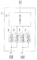
- FIG. 1 is a configuration diagram showing the configuration of the distance measuring apparatus 100 according to the first or second embodiment.
- a distance measuring apparatus 100 shown in FIG. 1 includes a light emission exposure control unit 101, a solid-state imaging device 102, a signal processing unit 103, and a light emitting unit 104.
- Examples of the solid-state image sensor 102 include a CCD (Charge Coupled Device) image sensor, a CMOS (Complementary Metal-Oxide Semiconductor) image sensor, and the like.
- CCD Charge Coupled Device
- CMOS Complementary Metal-Oxide Semiconductor
- the light emitting unit 104 includes a light source driving unit 114 and a light source 115.
- Examples of the light source 115 include an LED and a laser diode.
- the signal processing unit 103 includes a line memory 111, a combining unit 112, and a distance calculating unit 113.
- the light emission exposure control unit 101 generates and outputs a light emission timing signal LT1, an exposure timing signal ET1, and a shutter timing signal SH1 according to predetermined conditions described later.
- the light source driving unit 114 in the light emitting unit 104 is ON / OFF controlled by the light emission timing signal LT1, and the light source 115 emits the light L1 toward the object OBJ.
- the irradiation light L1 is light with a pulse waveform having a predetermined emission width.
- the irradiation light L1 is reflected by the object OBJ.
- the reflected light L2 is received by the solid-state image sensor 102 via a lens optical system (not shown).
- the solid-state image sensor 102 has a plurality of pixels arranged in a matrix. In the solid-state imaging device 102, exposure at each pixel is controlled according to the exposure timing signal ET1 and the shutter timing signal SH1. A pixel signal corresponding to the signal charge photoelectrically converted and accumulated in each pixel is output to the signal processing unit 103.
- FIG. 2 is a diagram showing an example of the TOF method.
- a delay time among the reflected light that is time-delayed due to the S0 exposure for receiving all the reflected light of the light emitted in a pulse form from the light source and the distance of the object reflected by the pulse light emitted from the light source.
- S1 exposure for receiving a part of the reflected light corresponding to the minute and BG exposure for receiving only the background light without causing the light source to emit light are performed.
- background light is also received simultaneously.
- T0 is the light emission pulse width (irradiation pulse time width)
- c is the speed of light
- FIG. 3 is a diagram showing another example of the TOF method.
- the length of the exposure period of the solid-state imaging device is substantially the same as the light emission pulse width in comparison with the method of FIG. 2, and the pulse light emission timing of the irradiation light and the outline of the reflected light reflected from the object and returned after being delayed.
- the S0 exposure for receiving light in the same exposure period and the S1 exposure for receiving a part of the reflected light returned after completion of the pulse emission of the irradiation light are obtained.
- the distance L to the object OBJ can be obtained by Expression 2.
- the timing of the exposure signal and the formula for calculating the distance are not limited to this.
- the irradiation light is emitted in a sine wave shape, and the reflected light is exposed at a timing corresponding to a phase of 0 degrees, a phase of 90 degrees, a phase of 180 degrees, and a phase of 270 degrees with respect to the phase of the sine wave of the irradiation light.
- four pixel signals are acquired for each pixel group.
- the time difference of the reflected light with respect to the irradiation light is determined from the ratio of the difference signal between the pixel signal of 0 degree phase and the pixel signal of 180 degree phase, the difference signal of the pixel signal of 90 degree phase and the pixel signal of 270 degree phase. Can be calculated and converted into distance.
- the pixel signal group (S0, S1, BG) input to the signal processing unit 103 is held in the line memory 111 in units of lines corresponding to the pixels of the solid-state image sensor 102.
- the synthesizing unit 112 inputs a pixel signal of a necessary reference pixel from the line memory 111 and performs a synthesizing process.
- the result of the combining process performed by the combining unit 112 is input to the distance calculation unit 113, and the distance calculation unit 113 calculates the expression 1 or 2 using the combined pixel signal, and the distance obtained as a result of the calculation.
- the value D0 is output.
- the exposure timing signal ET1 output from the light emission exposure control unit 101 is, specifically, two sets of the above three exposure signals for S0 exposure, S1 exposure, and BG exposure.
- the light emission exposure control unit 101 outputs the signal group to the solid-state image sensor 102.
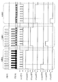
- FIG. 4 is a schematic configuration diagram of a solid-state imaging device in the distance measuring device according to the present embodiment.
- FIG. 4 shows an example of the connection relationship between the pixel cell arrangement of the solid-state image sensor 102 and the exposure timing signal group.
- P01, P02, P03,... In FIG. 4 indicate each pixel cell including the photodiode region.
- Each pixel cell is arranged with the pixel position shifted by a half pixel pitch in the horizontal direction in the odd-numbered line and the even-numbered line in line units.
- Three signals of exposure timing signals ET10a, ET11a, and ET12a are connected to the pixel cells of the odd lines, and three signals of ET10b, ET11b, and ET12b are connected to the pixel cells of the even lines.
- the line for supplying the shutter timing signal SH1 is commonly connected to all the pixel cells.
- FIG. 5 shows an example of a schematic configuration diagram of a pixel cell of a solid-state imaging device in the distance measuring device according to the present embodiment.
- the reset transistor 502 is connected to the photodiode 501 that performs photoelectric conversion, and when the shutter timing signal SH1 is turned on, the charge photoelectrically converted by the photodiode is discarded.
- analog memories 520, 521, and 522 are connected to the photodiode 501 through analog switches 510, 511, and 512, respectively.
- the exposure timing signal ET10a is supplied for ON / OFF control of the analog switch 510
- the exposure timing signal ET11a is supplied for ON / OFF control of the analog switch 511
- the analog switch 512 is turned ON.
- An exposure timing signal ET12a is supplied for control of / OFF.
- the exposure timing signal ET10b is connected to the ON / OFF control of the analog switch 510
- the exposure timing signal ET11b is supplied to control the analog switch 511 ON / OFF
- the analog switch 512 is turned ON.
- An exposure timing signal ET12b is supplied for controlling / OFF.
- the analog memories 520, 521, and 522 store charges photoelectrically converted by the photodiode 501 during a period in which the analog switches 510, 511, and 512 to be connected are ON and a non-reset period in which the reset transistor 502 is OFF. . In addition, the analog memories 520, 521, and 522 do not accumulate charges during a period in which the analog switches 510, 511, and 512 are ON and a period in which the reset transistor 502 is in an ON state or a period in which the analog switches 510, 511, and 512 are in an OFF state. .
- the solid-state imaging device 102 can perform exposure control independently for each of odd-numbered lines and even-numbered lines.
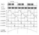
- FIG. 6A and 6B show an example of the relationship between the exposure timing signal output from the light emission exposure control unit 101, the irradiation light, and the shutter timing signal SH1, as a first example of light emission exposure control.
- FIG. 6A is a light emission exposure control timing chart in the distance measuring apparatus according to the present embodiment.
- the pulsed irradiation light generated by the light emission timing signal LT1 generated and output by the light emission exposure control unit 101, and the exposure timing signal ET1 and the shutter timing signal SH1 generated and output by the light emission exposure control unit 101 are as shown in FIG. 6A.
- the same pattern is output repeatedly for a plurality of cycles with one cycle.
- the one cycle time (exposure period cycle Tcyc) is, for example, 1 of the light amount fluctuation cycle (light source cycle time Tbg) of illumination light using a commercial AC power source as a power source in the environment where the distance measuring apparatus 100 is used.
- / N (n is an integer of 2 or more).
- the number of cycles Ncyc is generally set to n ⁇ m (m is an integer of 1 or more).
- the present invention is not limited to this.
- FIG. 6B shows an enlarged one cycle period of FIG. 6A described above.
- the one-cycle period is a period for performing the S0 exposure formed by the shutter timing signal SH1 that generates the timing at which the light emission exposure control unit 101 is turned on based on the TOF method 1 shown in FIG. And a period for performing S1 exposure and a period for performing BG exposure.
- the exposure timing signals ET10a and ET10b are supplied during the S0 exposure period, the exposure timing signals ET11a and ET11b are supplied during the S1 exposure period, and the exposure timing signals ET12a and ET12b are supplied during the BG exposure period.
- the ET10a signal is supplied for a period of 8 pulses of pulsed irradiation light generated by the light emission timing signal LT1
- the ET11b signal is supplied only for a period of 2 pulses.
- the time (first condition) during which photoelectric conversion is performed on pixels in odd lines of the solid-state imaging device 102 and signals are accumulated in the analog memory 520
- the time in which signals are accumulated in analog memories 520 of pixels in the even lines. (Second condition) is a relationship in which the ratio of signal accumulation time corresponding to exposure time is 4: 1.
- the control example in which the ratio of the exposure time is 4: 1 is shown.
- the present invention is not limited to this.
- the exposure timing ratio can be easily changed by changing the timing control described above. Can be formed.
- S0odd can be expressed by Equation 3.
- Equation 3 A0odd represents a signal component due to irradiation light, and B0odd represents a signal component due to background light.
- S1odd the signal accumulated in the analog memory 521 of one pixel cell in the odd-numbered line of the solid-state imaging device 102 by S1 exposure.
- Equation 4 A1odd represents a signal component due to irradiation light, and B1odd represents a signal component due to background light.
- the signal accumulated in the analog memory 521 of one pixel cell in the odd-numbered line of the solid-state image sensor 102 by BG exposure is defined as BGodd.
- S0evn a signal accumulated in the analog memory 520 of one pixel cell in the even-numbered line of the solid-state imaging device 102 by the S0 exposure and in the vicinity of one pixel in the odd-numbered line.
- S0evn can be expressed by Equation 5.
- Equation 5 A0evn represents a signal component due to irradiation light, and B0evn represents a signal component due to background light.
- S1evn can be expressed by Equation 6.
- Equation 6 A1evn represents a signal component due to irradiation light, and B1evn represents a signal component due to background light.
- the signal accumulated in the analog memory 521 by BG exposure on the other pixel of the even-numbered line of the solid-state image sensor 102 is defined as BGevn.
- Equation (7) is established between these pixels and even-numbered pixels.
- A0odd 4 ⁇ A0evn
- A1odd 4 ⁇ A1evn ...
- each pixel signal of BG exposure is performed in six periodic exposure periods in this embodiment.
- the period of each exposure period is 1/3 period with respect to 1 period of the light quantity fluctuation
- the electric charge photoelectrically converted by the solid-state imaging device 102 in each exposure period is stored in each analog memory 520, 521, and 522 sequentially without exposing the magnitude of the background light, so that the S0 signal, the S1 signal, The background light components of the pixel signals of each BG signal are averaged. Therefore, Formula 8 is satisfied regardless of the fluctuation of the background light.
- Equation 9 is established, and only the signal component of the illumination light from which the background light component has been removed can be accurately extracted.
- A0odd S0odd ⁇ BGodd
- A1odd S1odd ⁇ BGodd
- A0evn S0evn ⁇ BGevn
- A1evn S1evn ⁇ BGevn ....
- Equation 10 is satisfied without being affected by the disturbance even under illumination light whose intensity varies with a commercial AC power source or the like.
- the light emission exposure control unit 101 of the first example of light emission exposure control With the operation of the light emission exposure control unit 101 of the first example of light emission exposure control, exposure control with different exposure times is performed in the same frame of the solid-state image sensor under an environment where illumination light using a commercial AC power source becomes noise. Even if it implements by, the signal of the background light component which receives the fluctuation
- a pixel whose exposure time is relatively short with respect to one period of fluctuation in the amount of illumination light using a commercial AC power source as a power source is affected by the local bias of the background light that fluctuates.
- the background light components of the S0 signal and the S1 signal are averaged by averaging the local sizes of the background light. Since it becomes equal to the BG signal, the illumination light component signals of S0 exposure and S1 exposure can be extracted with high accuracy.
- FIG. 7 shows a second example of light emission exposure control.
- the light emission control timing control method shown in FIG. 7 is a control method different from the light emission exposure timing control method shown in FIG. 6A.
- the light emission control timing control method shown in FIG. 7 takes time to emit illumination light for exposing odd lines as the first condition and illumination light for exposing even lines as the second condition. Are separated.
- the exposure timing and the exposure period of the odd and even lines are separated in time.
- the stray light reflected by the inner surface of the lens disposed on the front surface of the solid-state imaging device 102 or the object having a high light reflectance in the irradiation range of the irradiation light which is not the target of the exposure period of the second condition
- the stray light generated by the secondary reflection of the reflected light flying to the object reaches the second condition exposure period with a time delay due to the long flight distance.
- Optical effects on the pixel signal can be avoided.
- the solid-state imaging device 102 After the exposure shown in FIG. 6A or FIG. 7 is performed by a built-in timing generator (not shown) or the like, the solid-state imaging device 102 sequentially scans the S0 signal, the S1 signal, and the BG signal for each pixel on the pixel array. Read sequentially. The read S0 signal, S1 signal, and BG signal for each pixel are output to the signal processing unit 103.
- the pixel signal input from the solid-state imaging device 102 is received by the line memory 111 in the signal processing unit 103 in a predetermined number of S0odd signals, S1odd signals, and BGodd signals for odd lines, and S0evn for a predetermined number of even lines.
- the signal, the S1evn signal, and the BGevn signal are sequentially stored and held, and the pixel signal to be referred to is sequentially output to the combining unit 112.
- FIG. 8 is a configuration diagram of a combining unit in the distance measuring device according to the first embodiment.
- the combining unit 112 includes a combining calculation processing unit 801, a first condition background light removal unit 802, a first condition saturation determination unit 803, and a second condition background light removal. Part 804 and a saturation determination part 805 for the second condition.
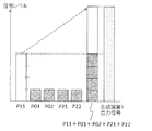
- FIG. 9 is a pixel diagram referred to by the combining unit 112 in the distance measuring apparatus according to the present embodiment.
- the synthesizer 112 sets the S0 signal of each pixel as a pixel group for processing one pixel of the odd line and four pixels of the even line adjacent to the upper and lower lines from the line memory 111 as shown in FIG. , S1 signal and BG signal are input from the line memory 111.
- the pixel group P01, P02, P11, P21, and P22 in FIG. 9 is a set of processing target pixels.
- a set of P02, P03, P12, P22, and P23, and P21, P22, P31, P41, One set of P42 is sequentially input to the combining unit 112 and combined.
- P01, P02, P11, P21, and P22 that are the target pixel group A in FIG. 9 are taken as an example.
- the input signals S0odd (P11), S1odd (P11), and BGodd (P11) of one pixel in the odd lines are the background light removing unit 802 and the first condition of the first condition. Is input to the saturation determination unit 803.
- S0odd (P11) represents the S0odd signal of the pixel P11
- S1odd (P11) represents the S1odd signal of the pixel P11
- BGodd (P11) represents the BGodd signal of the pixel P11.
- Formula 11 is computed and A0odd (P11) and A1odd (P11) are output to the synthesis computation processing unit 801.
- A0odd (P11) S0odd (P11) ⁇ BGodd (P11)
- A1odd (P11) S1odd (P11) ⁇ BGodd (P11) ....
- the first condition saturation determination unit 803 performs the condition determination of Expression 12 on the saturation determination threshold Smax set in advance corresponding to the output signal range of the solid-state imaging device 102.
- the saturation determination unit 803 of the first condition notifies the synthesis calculation processing unit 801 that there is a saturation signal when any of the conditions of Expression 12 is satisfied.
- Equation 13 is calculated and executed, and A0evn (P01), A1evn (P01), A0evn (P02), A1evn (P02), A0evn (P21), A1evn (P21), A0evn. (P22), A1evn (P22) is output to the composition calculation processing unit 801.
- A0evn (P01) S0evn (P01) ⁇ BGevn (P01)
- A1evn (P01) S1evn (P01) ⁇ BGevn (P01)
- A0evn (P02) S0evn (P02) ⁇ BGevn (P02)
- A1evn (P02) S1evn (P02) ⁇ BGevn (P02)
- A0evn (P21) S0evn (P21) ⁇ BGevn (P21)
- A1evn (P21) S1evn (P21) ⁇ BGevn (P21)
- A0evn (P22) S0evn (P22) ⁇ BGevn (P22)
- A1evn (P22) S1evn (P22) ⁇ BGevn (P22) .... Formula 13
- the condition determination of Expression 14 is performed on the above-described threshold value Smax.
- the saturation determination unit 805 of the second condition notifies the synthesis calculation processing unit 801 that there is a saturation signal when any of the conditions is satisfied.
- FIG. 10 is a flowchart showing the procedure of the composition calculation process in the distance measuring device 100 according to the present embodiment.
- the saturation determination unit 805 of the second condition determines whether there is a saturation signal as described above (step S1001). If there is a saturation signal (Y in step S1001), the saturation determination unit 805 of the second condition notifies the composition calculation processing unit 801 that there is a saturation signal. In this case, the composition calculation processing unit 801 performs distance measurement impossibility processing (step S1005).
- the composition calculation processing unit 801 outputs a distance measurement impossible state to the distance calculation unit 113.
- the saturation determination unit 803 of the first condition determines whether there is a saturation signal (step S1002). If there is a saturation signal (Y in step S1002), the saturation determination unit 803 under the first condition notifies the synthesis calculation processing unit 801 that there is a saturation signal. In this case, the synthesis calculation processing unit 801 performs the synthesis calculation 2 (step S1004). If there is no saturation signal, the synthesis operation processing unit 801 performs the synthesis operation 1 (step S1003).
- the synthesis operation processing unit 801 executes the operation of Expression 15, and calculates A0mix and A1mix.
- the data is output to the distance calculation unit 113.
- A0mix A0odd (P11) + A0evn (P01) + A0evn (P02) + A0evn (P21) + A0evn (P22)
- A1mix A1odd (P11) + A1evn (P01) + A1evn (P02) + A1evn (P21) + A1evn (P22) ....
- FIG. 11A is a diagram illustrating a relationship between the signal amount obtained by the synthesis calculation 1 and the input signal in the distance measuring device according to the first embodiment.
- the exposure time ratio is 4: 1 in the first condition and the second condition
- a signal amount that is eight times the signal amount obtained from the pixel under the second condition is obtained by the synthesis operation 1. Will be. Therefore, a high S / N ratio can be realized by the synthesis operation 1.
- a low-pass filter having symmetrical characteristics in the horizontal and vertical directions of 1: 3: 3: 1 in the half period of the pixel pitch in the horizontal direction and 1: 2: 1 in the period of the pixel pitch in the vertical direction. Therefore, there is no spatial sampling point bias.
- the synthesis calculation processing unit 801 executes the calculation of Expression 16 using only the pixel signal obtained under the second condition, and outputs A0mix and A1mix to the distance calculation unit 113.
- A0mix ⁇ A0evn (P01) + A0evn (P02) + A0evn (P21) + A0evn (P22) ⁇ ⁇ K
- A1mix ⁇ A1evn (P01) + A1evn (P02) + A1evn (P21) + A1evn (P22) ⁇ ⁇ K ....
- the coefficient K in Equation 16 is determined in advance from the ratio of the total value of one pixel for the exposure time of the first condition and the total value of four pixels for the exposure time of the second condition.
- the exposure time of the second condition is a, in the present embodiment, it is 2 which is a value calculated from the following.
- FIG. 11B shows a relationship diagram between the signal amount obtained by the synthesis operation 2 and the input signal.
- a spatial low-pass filter or a bilateral filter is combined with the synthesis unit 112 and the distance calculation unit 113 for further reduction of signal noise.
- the reference pixel group of this spatial filter even if the pixel signal exposed under the first condition is mixed with or without saturation, the continuity of the signal amount is maintained and the filter is normally filtered. Processing can be executed.
- the above is the description of the first example of the combining unit 112.
- FIG. 11B is a diagram illustrating the relationship between the signal amount obtained by the synthesis calculation 2 and the input signal in the distance measuring device 100 according to the present embodiment.
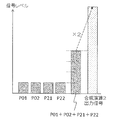
- FIG. 12 is a pixel diagram referred to in the synthesis unit 112.
- the synthesizer 112 sets one pixel of the odd line and one pixel of the even line adjacent to the pixel on the upper side or the lower side as a pixel group to be processed.
- the S0 signal, S1 signal and BG signal of each pixel are input from the line memory 111.
- the pixel group of P01 and P11 in FIG. 12 is a set of pixels to be processed, and a set of P02 and P11 or a set of P11 and P21 is sequentially input to the combining unit for signal processing.
- P01 and P11 which are the target pixel group B in FIG. 12 will be described as an example.
- the internal configuration of the synthesis unit 112 that performs the synthesis operation 2 is the same as that in FIG.
- the input signals S0odd (P11), S1odd (P11), and BGodd (P11) of one pixel in the odd line are input to the background light removing unit 802 under the first condition and the saturation determining unit 803 under the first condition.
- the saturation determination unit 803 of the first condition performs the same condition determination as that of the above-described Expression 12, and compares the previously set threshold value Smax with S0odd (P11), S1odd (P11), and BGodd (P11), respectively. To do. When any one of the input signals satisfies a large condition, the saturation determination unit 803 of the first condition notifies the synthesis calculation processing unit 801 that there is a saturation signal.
- the input signals S0evn (P01), S1evn (P01), and BGevn (P01) of one pixel in the even line are input to the background light removal unit 804 of the second condition and the saturation determination unit 805 of the second condition.
- Equation 17 is calculated and executed, and A0evn (P01), A1evn (P01), and A0evn (P02) are output to the synthesis calculation processing unit 801.
- A0evn (P01) S0evn (P01) ⁇ BGevn (P01)
- A1evn (P01) S1evn (P01) ⁇ BGevn (P01) ....
- the second condition saturation determination unit 805 performs the condition determination of Expression 18 with respect to the above-described threshold value Smax. When either condition is satisfied, the saturation determination unit 805 of the second condition notifies the synthesis calculation processing unit 801 that there is a saturation signal sum.
- the processing procedure of the composite operation processing unit 801 is the same as that shown in FIG. 10, but the calculation methods of the composite operation 1 and the composite operation 2 are different.
- the synthesis calculation processing unit 801 executes the calculation of Formula 19, and outputs A0mix and A1mix to the distance calculation unit 113.
- A0mix A0odd (P11) + A0evn (P01) ⁇ K2
- A1mix A1odd (P11) + A1evn (P01) ⁇ K2 ....
- the coefficient K2 in Equation 19 is determined in advance from the ratio of the exposure time of the first condition and the exposure time of the second condition, and this embodiment assumes that the exposure time of the second condition is a. Then, it is 4 which is a value calculated from the following.
- FIG. 13A is a diagram illustrating the relationship between the signal amount obtained by the synthesis operation 1 and the input signal.
- the synthesis operation processing unit 801 executes the operation of Expression 20 using only the pixel signal obtained under the second condition, and outputs A0mix and A1mix to the distance calculation unit 113.
- A0mix A0evn (P01) ⁇ K3
- A1mix A1evn (P01) ⁇ K3 ....
- the coefficient K3 in Expression 20 is calculated in advance from the ratio of the total value of one pixel of the exposure time of the first condition and the value four times the exposure time of the second condition and the exposure time of the second condition. If the exposure time under the second condition is a, the value calculated from the following is 8 in the present embodiment.
- FIG. 13B is a diagram illustrating the relationship between the signal amount obtained by the synthesis operation 2 and the input signal.
- the effect of unifying the signal amount and scale obtained by the synthesis operation 1 by multiplying by the coefficient K3 is as described in the first example of the synthesis unit 112.
- the pixel signal after the synthesizing process is obtained even though the exposure time is different between the odd-numbered line and the even-numbered line of the solid-state imaging device 102 to ensure a wide measurable range.
- the combined A0mix and A1mix output from the synthesis calculation processing unit 801 are input to the distance calculation unit 113 as the output of the synthesis unit 112.
- the distance calculation unit 113 When the distance calculation unit 113 is notified of the above-mentioned distance measurement impossible state from the combination calculation processing unit 801, the distance calculation unit 113 outputs the output signal DO with a value indicating a predetermined measurement impossible state. When the distance measurement impossible state has not been notified, the composition calculation processing unit 801 calculates the output signal DO using Equation 21.
- Equation 21 is an equation equivalent to Equation 2 corresponding to the TOF method 1 described in FIG. 2, the output signal DO is a value corresponding to the distance to the object.
- the distance calculation unit 113 may be expressed by the following equation (22).
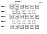
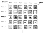
- FIG. 14 is a pixel arrangement of the solid-state imaging device 102 in the distance measuring device 100 according to the present embodiment and a pixel diagram referred to by the combining unit 112.
- FIG. 14 shows the arrangement of pixel cells of the solid-state imaging device 102, the configuration of each pixel group, and the combination of pixels referred to by the combining unit 112. In the following, the description will mainly focus on differences from the first embodiment.
- the solid-state image sensor 102 includes pixels of even lines and even columns (hereinafter referred to as first pixel group), pixels of even lines and odd columns (hereinafter referred to as second pixel group), pixels of odd lines and even columns. Independent exposure control is possible for each of the four pixel groups (hereinafter, the third pixel group) and the pixels in the odd lines and the odd columns (hereinafter, the fourth pixel group).
- the pixel P01 is the first pixel group
- the pixel P02 is the second pixel group
- the pixel P11 is the third pixel group
- the pixel P12 is the fourth pixel group.
- these pixels will be described as an example.
- the exposure timing signal ET1 output from the light emission exposure control unit 101 is one of three exposure signals for S0 exposure, S1 exposure, and BG exposure as described above. It consists of four sets of signals.
- the ET10a signal, the ET11a signal, and the ET12a signal are supplied to the first pixel group including the pixel P01.
- the ET10b signal, the ET11b signal, and the ET12b signal are supplied to the second pixel group including the pixel P02.
- the ET10c signal, the ET11c signal, and the ET12c signal are supplied to the third pixel group including the pixel P11.
- the ET10d signal, the ET11d signal, and the ET12d signal are supplied to the fourth pixel group including the pixel P12.
- FIG. 15 is a light emission exposure control timing chart in the distance measuring apparatus 100 according to the present embodiment.
- the operation of the light emission exposure control unit 101 of the present embodiment allows exposure with different exposure times for each of the four pixel groups in an environment in which illumination light using a commercial AC power source becomes noise. Even if the control is performed in the same frame of the solid-state imaging device, the signal of the background light component that receives the fluctuation of the illumination light intensity can be averaged. Thereby, it is possible to eliminate the bias of the signal amount of the background light component between the S0 exposure, the S1 exposure, and the BG exposure from the first pixel group to the fourth pixel group of the solid-state imaging device 102. In particular, it is possible to accurately extract the illumination light component signals of the S0 exposure and S1 exposure of each pixel of the third pixel group or the fourth pixel group that have a relatively short exposure time.
- FIG. 14 also shows the relationship of the pixel groups that the combining unit 112 in the signal processing unit 103 refers to at the time of combining as this embodiment.
- the synthesizer 112 receives one pixel from the adjacent first pixel group, one pixel from the second pixel group, one pixel from the third pixel group, and the first pixel from the line memory 111.
- the S0 signal, the S1 signal, and the BG signal of each pixel are input from the line memory 111 as a pixel group for processing four pixels of one pixel of the four pixel groups.
- P01, P02, P11, and P12 in FIG. 14 are a set of processing target pixel groups, and as other combinations, a set of P03, P04, P13, and P14, or a set of P21, P22, P31, and P32 Are sequentially input to the combining unit 112 to be combined.
- the target pixel group C in FIG. 14 will be described by taking P01, P02, P11, and P12 as an example.
- FIG. 16 is a configuration diagram of the synthesis unit 112 in the distance measuring apparatus 100 according to the present embodiment.
- the combining unit 112 includes a combining calculation processing unit 1601, a background light removing unit 1602 of the first pixel group, a saturation determining unit 1603 of the first pixel group, A background light removal unit 1604 of the second pixel group, a saturation determination unit 1605 of the second pixel group, a background light removal unit 1606 of the third pixel group, a saturation determination unit 1607 of the third pixel group, A background light removing unit 1608 for the fourth pixel group, and a saturation determining unit 1609 for the fourth pixel group.
- S0g1 (P01) which is the S0 signal, S1g1 (P01) which is the S1 signal, and BGg1 (P01) which is the BG signal are the first pixel group.
- the background light removal unit 1602 and the saturation determination unit 1603 of the first pixel group are input.
- Expression 23 is calculated and A0g1 (P01) and A1g1 (P01) are output to the combination calculation unit 1601.
- A0g1 (P01) S0g1 (P01) ⁇ BGg1 (P01)
- A1g1 (P01) S1g1 (P01) ⁇ BGg1 (P01) ....
- the saturation determination unit 1603 of the first pixel group performs the condition determination of Expression 24 on the saturation detection threshold Smax, and if any of the conditions is satisfied, The pixel group saturation determination unit 1603 notifies the synthesis calculation processing unit 1601 that there is a saturation signal.
- the input signals S0g2 (P02), S1g2 (P02), and BGg2 (P02) of the pixel P02 of the second pixel group are the same as the pixel P01.
- the background light removal unit 1604 of the second pixel group calculates A0g2 (P02) and A1g2 (P02), and outputs them to the synthesis operation processing unit 1601.
- the saturation determination unit 1605 of the second pixel group notifies the synthesis calculation processing unit 1601 of the presence or absence of any one of S0g2 (P02), S1g2 (P02), and BGg2 (P02).
- the input signals S0g3 (P11), S1g3 (P11), and BGg3 (P11) of the pixel P11 of the third pixel group are the same as the pixel P01.
- the background light removal unit 1606 of the third pixel group calculates A0g3 (P11) and A1g3 (P11), and outputs them to the synthesis operation processing unit 1601.
- the saturation determination unit 1607 of the third pixel group notifies the synthesis calculation processing unit 1601 of the presence / absence of any one of S0g3 (P11), S1g3 (P11), and BGg3 (P11).
- the input signals S0g4 (P12), S1g4 (P12), and BGg4 (P12) of the pixel P12 of the fourth pixel group are the same as the pixel P01.
- the background light removal unit 1608 of the fourth pixel group calculates A0g4 (P12) and A1g4 (P12), and outputs them to the synthesis operation processing unit 1601.
- the saturation determination unit 1609 of the fourth pixel group notifies the synthesis calculation processing unit 1601 of the presence / absence of one of S0g4 (P12), S1g4 (P12), and BGg4 (P12).
- FIG. 17 is a flowchart showing the procedure of the composition calculation process in the distance measuring device 100 according to the present embodiment.
- the saturation determination unit 1609 of the fourth pixel group determines whether or not there is a saturation signal (step S1701). If there is a saturation signal (Y in step S1701), the saturation determination unit 1609 of the fourth pixel group notifies the synthesis calculation processing unit 1601 that there is a saturation signal. In this case, the composition calculation processing unit 1601 performs a distance measurement impossible process (step S1705).
- the composition calculation processing unit 1601 outputs a distance measurement impossible state to the distance calculation unit 113.
- the saturation determination unit 1607 of the third pixel group determines whether there is a saturation signal (step S1702). If there is a saturation signal (Y in step S1702), the saturation determination unit 1607 of the third pixel group notifies the composition calculation processing unit 1601 that there is a saturation signal. In this case, the synthesis calculation processing unit 1601 performs the synthesis calculation 4 (step S1706).
- the saturation determination unit of the second pixel group determines whether there is a saturation signal (step S1703). If there is a saturation signal (Y in step S1703), the saturation determination unit 1605 of the second pixel group notifies the composition calculation processing unit 1601 that there is a saturation signal. In this case, the synthesis calculation processing unit 1601 performs the synthesis calculation 3 (step S1707).
- the saturation determination unit 1603 of the first pixel group determines whether there is a saturation signal (step S1704). If there is a saturation signal (Y in step S1704), the saturation determination unit 1603 of the first pixel group notifies the composition calculation processing unit 1601 that there is a saturation signal. In this case, the synthesis calculation processing unit 1601 performs the synthesis calculation 2 (step S1708).
- the synthesis operation processing unit 1601 performs the synthesis operation 1. In the synthesis operation 1, since all the pixels to be processed are output from the solid-state imaging device 102 within a normal signal range in a non-saturated state, the synthesis operation processing unit 1601 executes the operation of Expression 25 and calculates A0mix and A1mix. The data is output to the distance calculation unit 113.
- A0mix A0g1 (P01) + A0g2 (P02) + A0g3 (P11) + A0g4 (P12)
- A1mix A1g1 (P01) + A1g2 (P02) + A1g3 (P11) + A1g4 (P12) ....
- the output signal A0mix is 15 times the A0g4 signal of P12 having the shortest exposure time. Signal amount. Further, the output signal A1mix has a signal amount 15 times as large as the A1g4 signal of P12.
- the synthesis calculation processing unit 1601 executes the calculation of Expression 26 by removing the pixel signal of P01, and outputs A0mix and A1mix to the distance calculation unit 113.
- A0mix A0g2 (P02) + A0g3 (P11) + A0g4 (P12)
- A1mix A1g2 (P02) + A1g3 (P11) + A1g4 (P12) ....
- the synthesis calculation processing unit 1601 executes the calculation of Expression 27 by removing the pixel signals P01 and P02, and outputs A0mix and A1mix to the distance calculation unit 113.
- A0mix A0g3 (P11) + A0g4 (P12)
- A1mix A1g3 (P11) + A1g4 (P12) ....
- the composition calculation processing unit 1601 executes the calculation of Expression 28 and outputs A0mix and A1mix to the distance calculation unit 113.
- A0mix A0g4 (P12)
- A1mix A1g4 (P12) ....
- the operation of the distance calculation unit 113 is the same as in the first and second embodiments.
- the signal range can be expanded by 8 times the signal range of the solid-state imaging device 102 by independent exposure control of the four pixel groups. That is, the distance measuring device 100 according to the present embodiment can expand the distance measuring range that is a little less than three times in terms of distance compared to the distance measuring device 100 shown in the first embodiment.
- the exposure time ratio of the four pixel groups is not limited to the ratio described in the second embodiment, and can be easily changed by changing the timing of the exposure timing signal generated by the light emission exposure control unit 101. .
- the number of pixel groups for independently controlling the exposure time is four.
- the number of exposure timing signals generated by the light emission exposure control unit 101 is increased, and By increasing the number of divided wirings to each pixel cell in the solid-state imaging device 102, it is possible to easily increase the number of pixel groups that perform independent exposure control.
- the distance measurement range within one frame of the solid-state imaging device that is restricted by the attenuation of the light due to the distance of the target object or the reduction of the reflected light intensity due to the influence of the surface reflectance can be expanded to It is possible to realize a distance measuring apparatus that can acquire a distance image with good accuracy that is resistant to a change in the distance of a target object in a direction and that can eliminate the influence of disturbance due to background light other than irradiation light.
- a small and inexpensive distance measuring device that does not require a frame memory or the like can be realized.
- an on-board occupant detection device for example, an on-board occupant detection device, a monitoring system device for industrial FA application, and a human gesture motion by three-dimensionally detecting the movement of a person's arm or finger as a device for detecting the presence or absence of a person. It can be applied to an input device that recognizes and inputs a user interface of a specific device such as a PC.
- DESCRIPTION OF SYMBOLS 100 Distance measuring device 101 Light emission exposure control part 102 Solid-state image sensor 103 Signal processing part 104 Light emission part 111 Line memory 112 Synthesis
Abstract
In a distance measuring device (100) which uses a round-trip time of light to measure a distance to an object, a solid-state image capturing element (102) has a plurality of pixel groups the exposure of which can be controlled independently, and reflected light from the object, originating from pulsed light radiated by a light source (115), is received using a different exposure time for each pixel group. A light emission and exposure control unit (101) implements periodic intermittent exposure control for obtaining a plurality of types of pixel signals with different exposure times, corresponding to a time difference between the radiated light and the reflected light for each pixel group in the solid-state image capturing element (102), and a signal processing unit (103) obtains distance information to the object on the basis of pixel signals of adjacent pixels in pixel groups in the solid-state image capturing element (102) having different exposure times.
Description
本開示は、距離画像を生成する距離測定装置に関する。特に、照射光源とそれを受光する固体撮像素子で光の往復による遅延を用いて距離を測定する距離測定装置に関する。
The present disclosure relates to a distance measuring device that generates a distance image. In particular, the present invention relates to a distance measuring device that measures a distance using an irradiation light source and a solid-state imaging device that receives the light source and using a delay caused by reciprocation of light.
近年、距離画像を生成するための被写体の測距手法の一例として、赤外光またはレーザー光を被写体に向けて照射してから、被写体で反射した光を固体撮像装置で受光するまでの計測時間に基づいて被写体までの距離を算出(測距)するTOF(Time Of Flight)方式が知られている。
In recent years, as an example of a subject distance measurement method for generating a distance image, a measurement time from when infrared light or laser light is irradiated toward a subject until light reflected by the subject is received by a solid-state imaging device A TOF (Time Of Flight) method for calculating (ranging) the distance to a subject based on the above is known.
昨今のTOF方式は、被写体で反射した光を画素アレイを有する固体撮像素子により露光し、信号量を2次元面上に距離分布を示す距離画像として生成することで距離測定を行っている(例えば、特許文献1~3参照)。
In the recent TOF method, light reflected by a subject is exposed by a solid-state imaging device having a pixel array, and a signal amount is generated as a distance image indicating a distance distribution on a two-dimensional surface (for example, distance measurement is performed) Patent Documents 1 to 3).
しかしながら、従来の距離測定装置は、フレーム単位で時系列毎に異なる露光条件で距離画像を取得するため、距離測定可能な範囲が狭い装置では対象物の距離が変化した際に距離測定の精度が低下するという課題がある。また、従来の測距測定装置では、露出の異なる複数枚の距離画像を合成して距離を計測するため、距離画像に背景光などの照射光以外の外乱が含まれる場合、距離画像の露出にばらつきがあり、計測精度が安定しないという課題がある。
However, since the conventional distance measuring device acquires distance images under different exposure conditions for each time series in units of frames, the accuracy of distance measurement is improved when the distance of the object changes in an apparatus with a narrow distance measurable range. There is a problem of lowering. Further, in the conventional distance measuring device, since a distance is measured by combining a plurality of distance images with different exposures, when the distance image includes disturbances other than irradiation light such as background light, the exposure of the distance image is performed. There is a problem that there is variation and measurement accuracy is not stable.
このような課題に鑑み、本開示は、対象物の距離変化に影響されない距離測定範囲で、良好な精度で距離測定を行うことができる距離測定装置を提供することを目的とする。
In view of such a problem, an object of the present disclosure is to provide a distance measuring device capable of performing distance measurement with good accuracy in a distance measurement range that is not affected by a change in the distance of an object.
本開示の距離測定装置は、光の往復時間を利用して物体までの距離を測定する距離測定装置であって、光源から測定対象範囲に向けて光を照射する発光部と、前記発光部による照射光の画角内の前記物体の反射光を、行列状に配置された複数の画素において光電変換するとともに、前記画素の露光を独立して実施可能な複数の画素群を有する固体撮像素子と、前記発光部に対し前記光源の発光タイミングおよび発光期間を指示し、前記固体撮像素子の前記画素群ごとに光の往復時間に起因する照射光と反射光の時間差に対応する複数種類の画素信号を得るための露光タイミングと露光期間を指示し、前記露光タイミングと前記露光期間の指示を、前記画素群ごとの画素信号の露光を異なる露光時間で実施し、各前記画素群の照射光と反射光の時間差に対応する各画素信号の露光を周期的な少なくとも2つ以上の露光期間で実施することで、前記画素の露光を間欠的に行う発光露光制御部と、前記固体撮像素子の画素群ごとに異なる露光時間で露光を実施された2つ以上の近隣の画素の、照射光と反射光の時間差に対応した画素信号に基づいて、前記固体撮像素子に結像される物体の距離値を算出する信号処理部と、を備える。
A distance measuring device according to the present disclosure is a distance measuring device that measures a distance to an object using a round trip time of light, and includes a light emitting unit that emits light from a light source toward a measurement target range, and the light emitting unit. A solid-state imaging device having a plurality of pixel groups capable of photoelectrically converting reflected light of the object within an angle of view of irradiation light in a plurality of pixels arranged in a matrix and independently performing exposure of the pixels; Instructing the light emission timing and light emission period of the light source to the light emitting unit, and a plurality of types of pixel signals corresponding to the time difference between the irradiation light and the reflected light due to the round trip time of light for each pixel group of the solid-state imaging device The exposure timing and the exposure period are obtained, the exposure timing and the exposure period are instructed, and the pixel signal exposure for each of the pixel groups is performed at different exposure times, and the irradiation light and the reflection of each pixel group light By performing exposure of each pixel signal corresponding to the time difference in at least two or more periodic exposure periods, the light emission exposure control unit that intermittently exposes the pixels, and for each pixel group of the solid-state imaging device A distance value of an object imaged on the solid-state image sensor is calculated based on pixel signals corresponding to a time difference between irradiation light and reflected light of two or more neighboring pixels that have been exposed with different exposure times. A signal processing unit.
本開示の距離測定装置によれば、対象物の距離変化に影響されない距離測定範囲で、良好な精度で距離測定を行うことができる。
According to the distance measurement device of the present disclosure, it is possible to perform distance measurement with good accuracy in a distance measurement range that is not affected by a change in the distance of an object.
(本発明の基礎となった知見)
被写体の測距情報を有する画像(以下、距離画像)を生成する装置や手法は、近年、ゲームやアミューズメント分野だけでなく、車載カメラまたは監視カメラなどの2次元イメージセンサーが使用されてきた分野にも応用されている。 (Knowledge that became the basis of the present invention)
In recent years, not only games and amusement fields but also two-dimensional image sensors such as in-vehicle cameras or surveillance cameras have been used as apparatuses and methods for generating images having distance measurement information of subjects (hereinafter referred to as distance images). Has also been applied.
距離画像を生成するための被写体の測距手法には、複数のカメラを用いて撮像した画像の視差に基づいて距離画像を生成する方法、既知のランダムドットパターンを被写体に照射しドットパターンを受光する視差に基づいて距離画像を生成する方法などが存在する。それらの方法の一例であるTOF方式は、赤外光やレーザー光を被写体に向けて照射してから、被写体で反射した光を固体撮像装置で受光するまでの計測時間に基づいて被写体までの距離を算出(測距)する方式である。
The distance measurement method for generating a distance image includes a method for generating a distance image based on the parallax of images captured using multiple cameras, and irradiating the subject with a known random dot pattern to receive the dot pattern. There is a method of generating a distance image based on the parallax to be performed. The TOF method, which is an example of those methods, is a distance to a subject based on a measurement time from irradiation of infrared light or laser light toward the subject until light reflected by the subject is received by the solid-state imaging device. This is a method for calculating (ranging).
昨今のTOF方式は、被写体で反射した光を、画素アレイを有する固体撮像素子により露光し、得られた信号量より、固体撮像素子の画素毎に距離情報を取得することが可能であり2次元面上に距離分布を示す距離画像を生成することが可能である。
In the recent TOF method, light reflected from a subject is exposed by a solid-state imaging device having a pixel array, and distance information can be acquired for each pixel of the solid-state imaging device from the obtained signal amount. It is possible to generate a distance image showing a distance distribution on the surface.
当該技術では、固体撮像素子から被写体までの距離や被写体の表面反射率に応じて、受光する反射光の強度は大きく変動する。そこで、照射光源の強度や固体撮像素子の受光感度や露光量を一律にする。しかし、固体撮像素子の受光面に距離の異なる複数の対象物が存在する場合には、距離画像全体にわたって良好な測距性能を得ることが難しい。
In this technique, the intensity of the reflected light received varies greatly depending on the distance from the solid-state imaging device to the subject and the surface reflectance of the subject. Therefore, the intensity of the irradiation light source, the light receiving sensitivity of the solid-state imaging device, and the exposure amount are made uniform. However, when there are a plurality of objects having different distances on the light receiving surface of the solid-state imaging device, it is difficult to obtain good distance measurement performance over the entire distance image.
固体撮像素子で受光する反射光強度は、光源から被写体までの距離の二乗に反比例して減衰する光の特性または被写体表面の光反射率に依存する。例えば、反射光の露出調整を実施し露光量を増やすと、近距離にある物体や表面反射率の高い物体からの反射光は光強度が高くなり、固体撮像素子の受光可能な露光量を超えて飽和状態となる。この場合、正しい受光量信号を取得できなくなる。逆に、露光量を減らすと、遠距離にある物体または表面反射率の低い物体からの反射光量は微小となる。この場合には、安定した距離測定が困難になる。
The intensity of reflected light received by the solid-state imaging device depends on the characteristics of light that attenuates in inverse proportion to the square of the distance from the light source to the subject or the light reflectance of the subject surface. For example, if you adjust the exposure of reflected light and increase the amount of exposure, the reflected light from an object at a short distance or an object with high surface reflectance increases in light intensity, exceeding the exposure that can be received by the solid-state imaging device. And become saturated. In this case, a correct received light amount signal cannot be acquired. Conversely, when the exposure amount is reduced, the amount of reflected light from an object at a long distance or an object with low surface reflectance becomes minute. In this case, stable distance measurement becomes difficult.
上述のような技術的課題に対する解決手段として、特許文献1、特許文献2および特許文献3が開示されている。
Patent Document 1, Patent Document 2, and Patent Document 3 are disclosed as means for solving the technical problems as described above.
特許文献1および特許文献3では、露出の異なる複数枚の距離画像を取得し、それら複数画像から距離画像の合成を行い距離測定範囲の拡大と距離測定精度の向上を実施している。
In Patent Document 1 and Patent Document 3, a plurality of distance images with different exposures are acquired, and the distance images are synthesized from the plurality of images to expand the distance measurement range and improve the distance measurement accuracy.
特許文献2では、固体撮像素子において、偶数画素行と奇数画素行とで、それぞれ信号電荷の蓄積時間を個別に設定することにより異なる感度の信号を取り出し、これら感度の異なる信号を後段の信号処理系で合成する。具体的には、例えば、偶数行の各画素については蓄積時間を長く設定し高感度の画素信号を得て、奇数行の各画素については蓄積時間を短く設定し低感度の画素信号を得る。合成処理においては、偶数行の画素信号(高感度の画素信号)が飽和していない画素については高感度の画素信号を選択して利用し、飽和した画素については近傍の奇数行の画素信号(低感度の画素信号)を選択するといった合成処理が一般的である。
In Patent Document 2, in a solid-state imaging device, signals having different sensitivities are extracted by individually setting the signal charge accumulation time in each of even-numbered pixel rows and odd-numbered pixel rows, and signals having different sensitivities are processed in the subsequent signal processing. Synthesize in the system. Specifically, for example, for each pixel in an even row, the accumulation time is set long to obtain a highly sensitive pixel signal, and for each pixel in the odd row, a short accumulation time is set to obtain a low sensitivity pixel signal. In the combining process, a high-sensitivity pixel signal is selected and used for pixels in which even-numbered pixel signals (high-sensitivity pixel signals) are not saturated, and neighboring pixels in odd-numbered pixels ( A synthesis process such as selecting a low-sensitivity pixel signal) is generally used.
しかしながら、特許文献1または特許文献3の距離測定装置は、フレーム単位で時系列に異なる露光条件で距離画像を取得するため、対象物の距離が変化した際に距離測定の精度が低下する課題がある。さらに、当該測距測定装置では、露出の異なる複数枚の距離画像を記憶するため、固体撮像素子の画素毎の距離値を記憶するフレームメモリが必要となる。したがって、固体撮像素子の多画素化に伴い、より大容量のフレームメモリを必要とし、距離測定装置が大型かつ高価になるという問題がある。
However, since the distance measurement device of Patent Document 1 or Patent Document 3 acquires distance images under different exposure conditions in time series in units of frames, there is a problem in that the accuracy of distance measurement decreases when the distance of the object changes. is there. Furthermore, since the distance measuring device stores a plurality of distance images with different exposures, a frame memory for storing a distance value for each pixel of the solid-state imaging device is required. Therefore, with the increase in the number of pixels of the solid-state imaging device, there is a problem that a larger-capacity frame memory is required, and the distance measuring device is large and expensive.
また、特許文献2の合成処理では、高感度の画素信号が飽和していない場合は高感度の画素信号のみを利用するため、低感度の画素信号の画素情報は、有効であっても利用されないことになる。
Further, in the synthesis processing of Patent Document 2, since only the high-sensitivity pixel signal is used when the high-sensitivity pixel signal is not saturated, the pixel information of the low-sensitivity pixel signal is not used even if it is valid. It will be.
以下に説明する距離測定装置では、対象物体の距離による光の減衰または表面反射率の影響による反射光強度の低下により制約を受ける固体撮像素子の1フレーム内の距離測定範囲を拡大することで、時系列に沿った対象物の距離変化に強い距離画像を取得することができる。また、当該距離測定装置では、照射光以外の背景光による外乱の影響を除去することで、良好な精度の距離画像を取得することができる。これにより、フレームメモリ等を必要としない小型で低価格な距離測定装置の提供が可能となる。
In the distance measurement device described below, by expanding the distance measurement range within one frame of the solid-state imaging device that is restricted by the attenuation of light due to the distance of the target object or the decrease in reflected light intensity due to the influence of surface reflectance, It is possible to acquire a distance image that is resistant to changes in the distance of an object along a time series. In the distance measuring device, it is possible to acquire a distance image with good accuracy by removing the influence of disturbance due to background light other than irradiation light. As a result, it is possible to provide a small and inexpensive distance measuring device that does not require a frame memory or the like.
以下、本開示に係る実施形態について、図面を参照しながら詳細に説明する。
Hereinafter, embodiments according to the present disclosure will be described in detail with reference to the drawings.
(各実施形態における共通説明)
以下に説明する各実施形態では、被写体に対してLED光やレーザー光を照射して発生する反射光の往復時間を求めることで測距するTOF方式を用いる場合を例として説明する。 (Common description in each embodiment)
In each embodiment described below, an example will be described in which a TOF method is used in which distance measurement is performed by obtaining a round trip time of reflected light generated by irradiating a subject with LED light or laser light.
図1は、本実施形態1または2に係る距離測定装置100の構成を示す構成図である。図1に示す距離測定装置100は、発光露光制御部101、固体撮像素子102、信号処理部103および発光部104を備えている。
FIG. 1 is a configuration diagram showing the configuration of the distance measuring apparatus 100 according to the first or second embodiment. A distance measuring apparatus 100 shown in FIG. 1 includes a light emission exposure control unit 101, a solid-state imaging device 102, a signal processing unit 103, and a light emitting unit 104.
固体撮像素子102としては、CCD(Charge Coupled Device)イメージセンサーや、CMOS(Complementary Metal―Oxide Semiconductor)イメージセンサー等が挙げられる。
Examples of the solid-state image sensor 102 include a CCD (Charge Coupled Device) image sensor, a CMOS (Complementary Metal-Oxide Semiconductor) image sensor, and the like.
発光部104は、光源駆動部114と光源115から構成されている。光源115は、例えばLEDやレーザーダイオード等が挙げられる。
The light emitting unit 104 includes a light source driving unit 114 and a light source 115. Examples of the light source 115 include an LED and a laser diode.
信号処理部103は、ラインメモリ111、合成部112および距離演算部113から構成される。
The signal processing unit 103 includes a line memory 111, a combining unit 112, and a distance calculating unit 113.
発光露光制御部101は、後述の所定の条件に従って、発光タイミング信号LT1と露光タイミング信号ET1とシャッタータイミング信号SH1とを生成し出力する。発光タイミング信号LT1により発光部104内の光源駆動部114がON/OFF制御され、光源115が対象物OBJに向かって光L1を照射する。照射光L1は、所定の発光幅を持つパルス波形の光である。
The light emission exposure control unit 101 generates and outputs a light emission timing signal LT1, an exposure timing signal ET1, and a shutter timing signal SH1 according to predetermined conditions described later. The light source driving unit 114 in the light emitting unit 104 is ON / OFF controlled by the light emission timing signal LT1, and the light source 115 emits the light L1 toward the object OBJ. The irradiation light L1 is light with a pulse waveform having a predetermined emission width.
照射光L1は、対象物OBJで反射する。この反射光L2は、図示しないレンズ光学系を介して固体撮像素子102で受光される。固体撮像素子102は、行列状に配置された複数の画素を有している。固体撮像素子102において、露光タイミング信号ET1とシャッタータイミング信号SH1に従って各画素での露光が制御される。各画素で光電変換され蓄積された信号電荷に応じた画素信号は、信号処理部103へ出力される。
The irradiation light L1 is reflected by the object OBJ. The reflected light L2 is received by the solid-state image sensor 102 via a lens optical system (not shown). The solid-state image sensor 102 has a plurality of pixels arranged in a matrix. In the solid-state imaging device 102, exposure at each pixel is controlled according to the exposure timing signal ET1 and the shutter timing signal SH1. A pixel signal corresponding to the signal charge photoelectrically converted and accumulated in each pixel is output to the signal processing unit 103.
図2は、TOF方式の一例を示す図である。図2を用いてTOF方式の距離測定法の一例を説明する。TOF方式では、光源からパルス状に照射される光の反射光を全て受光するS0露光、光源から照射されるパルス光が反射した物体の距離に起因して時間遅延した反射光のうちで遅延時間分に相当する反射光の一部を受光するS1露光、および、光源を発光させずに背景光のみを受光するBG露光を行う。また、S0露光及びS1露光においては、背景光も同時に受光する。これらの3種類の露光を複数回ずつ繰り返して電荷を蓄積し、その蓄積した電荷量に応じた画素信号S0、S1、BGを得る。光源から対象物OBJまでの距離Lは、発光パルス幅(照射パルス時間幅)をT0、光の速度をcとすると、数式1で得られる。
FIG. 2 is a diagram showing an example of the TOF method. An example of a distance measurement method using the TOF method will be described with reference to FIG. In the TOF method, a delay time among the reflected light that is time-delayed due to the S0 exposure for receiving all the reflected light of the light emitted in a pulse form from the light source and the distance of the object reflected by the pulse light emitted from the light source. S1 exposure for receiving a part of the reflected light corresponding to the minute and BG exposure for receiving only the background light without causing the light source to emit light are performed. In S0 exposure and S1 exposure, background light is also received simultaneously. These three types of exposure are repeated a plurality of times to accumulate charges, and pixel signals S0, S1, and BG corresponding to the accumulated amount of charges are obtained. The distance L from the light source to the object OBJ can be obtained by Equation 1 where T0 is the light emission pulse width (irradiation pulse time width) and c is the speed of light.

図3は、TOF方式の他の例を示す図である。図2の方式に対して固体撮像素子の露光期間の長さが発光パルス幅と概同一となり、対象物から反射し遅延して戻ってきた反射光に対して、照射光のパルス発光タイミングと概同一の露光期間で受光するS0露光と、照射光のパルス発光完了より後に戻ってきた反射光の一部を受光するS1露光を得る。この場合の対象物OBJまでの距離Lは、数式2で得ることができる。
FIG. 3 is a diagram showing another example of the TOF method. The length of the exposure period of the solid-state imaging device is substantially the same as the light emission pulse width in comparison with the method of FIG. 2, and the pulse light emission timing of the irradiation light and the outline of the reflected light reflected from the object and returned after being delayed. The S0 exposure for receiving light in the same exposure period and the S1 exposure for receiving a part of the reflected light returned after completion of the pulse emission of the irradiation light are obtained. In this case, the distance L to the object OBJ can be obtained by Expression 2.

なお、露光信号のタイミングおよび距離計算式はこれだけに限定されるものではない。例えば、照射光をサイン波状に発光させて、照射光のサイン波の位相に対して0度の位相、90度の位相、180度の位相および270度の位相に相当するタイミングで反射光を露光して4つの画素信号を画素群ごとに取得する。そして、0度の位相の画素信号と180度の位相の画素信号の差分信号と90度の位相の画素信号と270度の位相の画素信号の差分信号との比から照射光に対する反射光の時間差を算出し、距離に換算する方法を取ることもできる。
Note that the timing of the exposure signal and the formula for calculating the distance are not limited to this. For example, the irradiation light is emitted in a sine wave shape, and the reflected light is exposed at a timing corresponding to a phase of 0 degrees, a phase of 90 degrees, a phase of 180 degrees, and a phase of 270 degrees with respect to the phase of the sine wave of the irradiation light. Thus, four pixel signals are acquired for each pixel group. Then, the time difference of the reflected light with respect to the irradiation light is determined from the ratio of the difference signal between the pixel signal of 0 degree phase and the pixel signal of 180 degree phase, the difference signal of the pixel signal of 90 degree phase and the pixel signal of 270 degree phase. Can be calculated and converted into distance.
信号処理部103に入力された画素信号群(S0、S1、BG)は、固体撮像素子102の画素に対応してライン単位で、ラインメモリ111に保持される。合成部112は、ラインメモリ111から必要な参照画素の画素信号を入力して合成処理を行う。合成部112で行われた合成処理の結果は距離演算部113に入力され、距離演算部113で合成後の画素信号を用いて数式1もしくは数式2の計算を行い、計算の結果得られた距離値D0を出力する。
The pixel signal group (S0, S1, BG) input to the signal processing unit 103 is held in the line memory 111 in units of lines corresponding to the pixels of the solid-state image sensor 102. The synthesizing unit 112 inputs a pixel signal of a necessary reference pixel from the line memory 111 and performs a synthesizing process. The result of the combining process performed by the combining unit 112 is input to the distance calculation unit 113, and the distance calculation unit 113 calculates the expression 1 or 2 using the combined pixel signal, and the distance obtained as a result of the calculation. The value D0 is output.
(第1の実施形態)
以下、第1の実施形態について説明する。本実施形態では、発光露光制御部101から出力される露光タイミング信号ET1は、詳細には前述のS0露光用、S1露光用、およびBG露光用の3つの露光用信号を1組とした2組の信号ET10a、ET11a、ET12aおよびET10b、ET11b、ET12bから構成されている。発光露光制御部101は、当該信号群を固体撮像素子102へ出力する。 (First embodiment)
The first embodiment will be described below. In the present embodiment, the exposure timing signal ET1 output from the light emissionexposure control unit 101 is, specifically, two sets of the above three exposure signals for S0 exposure, S1 exposure, and BG exposure. Signal ET10a, ET11a, ET12a and ET10b, ET11b, ET12b. The light emission exposure control unit 101 outputs the signal group to the solid-state image sensor 102.
以下、第1の実施形態について説明する。本実施形態では、発光露光制御部101から出力される露光タイミング信号ET1は、詳細には前述のS0露光用、S1露光用、およびBG露光用の3つの露光用信号を1組とした2組の信号ET10a、ET11a、ET12aおよびET10b、ET11b、ET12bから構成されている。発光露光制御部101は、当該信号群を固体撮像素子102へ出力する。 (First embodiment)
The first embodiment will be described below. In the present embodiment, the exposure timing signal ET1 output from the light emission
図4は、本実施形態に係る測距測定装置における固体撮像素子の概略構成図である。図4に固体撮像素子102の画素セルの配置と露光タイミング信号群の接続関係の一例を示す。図4中のP01、P02、P03・・・は、フォトダイオード領域を含む各画素セルを示している。
FIG. 4 is a schematic configuration diagram of a solid-state imaging device in the distance measuring device according to the present embodiment. FIG. 4 shows an example of the connection relationship between the pixel cell arrangement of the solid-state image sensor 102 and the exposure timing signal group. P01, P02, P03,... In FIG. 4 indicate each pixel cell including the photodiode region.
各画素セルは、ライン単位で奇数ラインと偶数ラインとにおいて画素位置が水平方向に半画素ピッチずらして配置されている。奇数ラインの画素セルには露光タイミング信号ET10a、ET11a、ET12aの3つの信号が接続され、偶数ラインの画素セルにはET10b、ET11b、ET12bの3つの信号が接続されている。なお、図示していないが、シャッタータイミング信号SH1を供給するラインは、すべての画素セルに共通して接続されている。
Each pixel cell is arranged with the pixel position shifted by a half pixel pitch in the horizontal direction in the odd-numbered line and the even-numbered line in line units. Three signals of exposure timing signals ET10a, ET11a, and ET12a are connected to the pixel cells of the odd lines, and three signals of ET10b, ET11b, and ET12b are connected to the pixel cells of the even lines. Although not shown, the line for supplying the shutter timing signal SH1 is commonly connected to all the pixel cells.
図5に、本実施形態に係る測距測定装置における固体撮像素子の画素セルの概略構成図を一例として示す。
FIG. 5 shows an example of a schematic configuration diagram of a pixel cell of a solid-state imaging device in the distance measuring device according to the present embodiment.
光電変換を行うフォトダイオード501にはリセットトランジスタ502が接続され、シャッタータイミング信号SH1がオンされるとフォトダイオードで光電変換された電荷は破棄される。
The reset transistor 502 is connected to the photodiode 501 that performs photoelectric conversion, and when the shutter timing signal SH1 is turned on, the charge photoelectrically converted by the photodiode is discarded.
さらに、フォトダイオード501にはアナログスイッチ510、511、512を介してアナログメモリー520、521、522がそれぞれ接続される。奇数ラインの画素セルでは、アナログスイッチ510のON/OFFの制御のために露光タイミング信号ET10aが供給され、アナログスイッチ511ON/OFFの制御のために露光タイミング信号ET11aが供給され、アナログスイッチ512のON/OFFの制御のために露光タイミング信号ET12aが供給される。同様に、偶数ラインの画素セルでは、アナログスイッチ510のON/OFF制御に露光タイミング信号ET10bが接続され、アナログスイッチ511ON/OFFの制御のために露光タイミング信号ET11bが供給され、アナログスイッチ512のON/OFFの制御のために露光タイミング信号ET12bが供給される。
Further, analog memories 520, 521, and 522 are connected to the photodiode 501 through analog switches 510, 511, and 512, respectively. In the odd-numbered pixel cells, the exposure timing signal ET10a is supplied for ON / OFF control of the analog switch 510, the exposure timing signal ET11a is supplied for ON / OFF control of the analog switch 511, and the analog switch 512 is turned ON. An exposure timing signal ET12a is supplied for control of / OFF. Similarly, in the pixel cells of even lines, the exposure timing signal ET10b is connected to the ON / OFF control of the analog switch 510, the exposure timing signal ET11b is supplied to control the analog switch 511 ON / OFF, and the analog switch 512 is turned ON. An exposure timing signal ET12b is supplied for controlling / OFF.
アナログメモリー520、521、522は、それぞれ接続されるアナログスイッチ510、511、512がON状態の期間かつリセットトランジスタ502がOFF状態の非リセット期間に、フォトダイオード501で光電変換された電荷を蓄積する。また、アナログメモリー520、521、522は、アナログスイッチ510、511、512がON状態の期間かつリセットトランジスタ502がON状態の期間またはアナログスイッチ510、511、512がOFF状態の期間には電荷蓄積しない。
The analog memories 520, 521, and 522 store charges photoelectrically converted by the photodiode 501 during a period in which the analog switches 510, 511, and 512 to be connected are ON and a non-reset period in which the reset transistor 502 is OFF. . In addition, the analog memories 520, 521, and 522 do not accumulate charges during a period in which the analog switches 510, 511, and 512 are ON and a period in which the reset transistor 502 is in an ON state or a period in which the analog switches 510, 511, and 512 are in an OFF state. .
上記の構成を取ることにより、固体撮像素子102は奇数ラインと偶数ラインの行毎に独立して露光制御が可能となる。
By adopting the above-described configuration, the solid-state imaging device 102 can perform exposure control independently for each of odd-numbered lines and even-numbered lines.
図6A及び図6Bに、発光露光制御の第1の例として、発光露光制御部101が出力する露光タイミング信号と照射光及びシャッタータイミング信号SH1との関係の一例を示す。図6Aは、本実施形態に係る測距測定装置における発光露光制御タイミング図である。
6A and 6B show an example of the relationship between the exposure timing signal output from the light emission exposure control unit 101, the irradiation light, and the shutter timing signal SH1, as a first example of light emission exposure control. FIG. 6A is a light emission exposure control timing chart in the distance measuring apparatus according to the present embodiment.
発光露光制御部101が生成し出力する発光タイミング信号LT1によって生じるパルス状の照射光と、発光露光制御部101が生成し出力する露光タイミング信号ET1およびシャッタータイミング信号SH1は、図6Aに示すように、同一のパターンを1サイクルとして、複数サイクル繰り返し出力される。当該1サイクルの時間(露光期間の周期Tcyc)は、例えば、距離測定装置100の使用される環境下で商用交流電源を電力源とする照明光の光量変動周期(光源の周期時間Tbg)の1/n(nは2以上の整数)とする。サイクル数Ncycは、n×m(mは1以上の整数)に概ね設定する。なお、図6Aでは、例としてn=3、m=2として総数6サイクルとしているが、これに限定するものではない。
The pulsed irradiation light generated by the light emission timing signal LT1 generated and output by the light emission exposure control unit 101, and the exposure timing signal ET1 and the shutter timing signal SH1 generated and output by the light emission exposure control unit 101 are as shown in FIG. 6A. The same pattern is output repeatedly for a plurality of cycles with one cycle. The one cycle time (exposure period cycle Tcyc) is, for example, 1 of the light amount fluctuation cycle (light source cycle time Tbg) of illumination light using a commercial AC power source as a power source in the environment where the distance measuring apparatus 100 is used. / N (n is an integer of 2 or more). The number of cycles Ncyc is generally set to n × m (m is an integer of 1 or more). In FIG. 6A, as an example, n = 3 and m = 2 and the total number of cycles is 6. However, the present invention is not limited to this.
図6Bに、上述した図6Aの1サイクル期間を拡大したものを示す。
FIG. 6B shows an enlarged one cycle period of FIG. 6A described above.
1サイクル期間は、前述の図2および数式1で示したTOF方式その1に基づいて、発光露光制御部101がON状態となるタイミングを生成したシャッタータイミング信号SH1により形成されるS0露光を行う期間と、S1露光を行う期間と、BG露光を行う期間とから構成されている。
The one-cycle period is a period for performing the S0 exposure formed by the shutter timing signal SH1 that generates the timing at which the light emission exposure control unit 101 is turned on based on the TOF method 1 shown in FIG. And a period for performing S1 exposure and a period for performing BG exposure.
S0露光の期間では、露光タイミング信号ET10aおよびET10bが供給され、S1露光の期間では、露光タイミング信号ET11aおよびET11bが供給され、BG露光の期間では、露光タイミング信号ET12aおよびET12bが供給される。
The exposure timing signals ET10a and ET10b are supplied during the S0 exposure period, the exposure timing signals ET11a and ET11b are supplied during the S1 exposure period, and the exposure timing signals ET12a and ET12b are supplied during the BG exposure period.
加えて、例えばS0露光ではET10a信号が発光タイミング信号LT1によって発生するパルス状の照射光の8パルス分の期間に供給されるのに対し、ET11b信号は2パルス分の期間に供給されるのみとし、前述の説明の通り固体撮像素子102の奇数ラインの画素で光電変換されアナログメモリー520に信号蓄積される時間(第1の条件)と、偶数ラインの画素のアナログメモリー520に信号蓄積される時間(第2の条件)は、露光時間に相当する信号蓄積時間の比率が4:1の関係となる。
In addition, for example, in the S0 exposure, the ET10a signal is supplied for a period of 8 pulses of pulsed irradiation light generated by the light emission timing signal LT1, whereas the ET11b signal is supplied only for a period of 2 pulses. As described above, the time (first condition) during which photoelectric conversion is performed on pixels in odd lines of the solid-state imaging device 102 and signals are accumulated in the analog memory 520, and the time in which signals are accumulated in analog memories 520 of pixels in the even lines. (Second condition) is a relationship in which the ratio of signal accumulation time corresponding to exposure time is 4: 1.
S1露光の期間、BG露光の期間についても同様である。
The same applies to the S1 exposure period and the BG exposure period.
なお、本実施形態では、露光時間の比率が4:1となる制御例を示したが、これに限定するものではなく、上述のタイミング制御の変形をすることで容易に異なる露光時間の比を形成することができる。
In the present embodiment, the control example in which the ratio of the exposure time is 4: 1 is shown. However, the present invention is not limited to this. The exposure timing ratio can be easily changed by changing the timing control described above. Can be formed.
上述のような発光と露光のタイミング制御で、S0露光によって固体撮像素子102の奇数ラインのひとつの画素セルのアナログメモリー520に蓄積された信号をS0oddとすると、S0oddは数式3で表せる。
If the signal accumulated in the analog memory 520 of one pixel cell of the odd-numbered line of the solid-state imaging device 102 by the S0 exposure is S0odd by the light emission and exposure timing control as described above, S0odd can be expressed by Equation 3.
S0odd=A0odd+B0odd ・・・・ 数式3
S0odd = A0odd + B0odd ... Formula 3
数式3において、A0oddは照射光による信号成分、B0oddは背景光による信号成分を示す。
In Equation 3, A0odd represents a signal component due to irradiation light, and B0odd represents a signal component due to background light.
S1露光によって固体撮像素子102の奇数ラインのひとつの画素セルのアナログメモリー521に蓄積された信号をS1oddとすると、S1oddは数式4で表せる。
Suppose that the signal accumulated in the analog memory 521 of one pixel cell in the odd-numbered line of the solid-state imaging device 102 by S1 exposure is S1odd, S1odd can be expressed by Equation 4.
S1odd=A1odd+B1odd ・・・・ 数式4
S1odd = A1odd + B1odd ... Formula 4
数式4において、A1oddは照射光による信号成分、B1oddは背景光による信号成分を示す。
In Equation 4, A1odd represents a signal component due to irradiation light, and B1odd represents a signal component due to background light.
BG露光によって固体撮像素子102の奇数ラインのひとつの画素セルのアナログメモリー521に蓄積された信号をBGoddとする。
The signal accumulated in the analog memory 521 of one pixel cell in the odd-numbered line of the solid-state image sensor 102 by BG exposure is defined as BGodd.
同様に、S0露光によって固体撮像素子102の偶数ラインのひとつの画素セルであって、上述の奇数ラインのひとつの画素の近傍にある画素セルのアナログメモリー520に蓄積された信号をS0evnとすると、S0evnは数式5で表せる。
Similarly, a signal accumulated in the analog memory 520 of one pixel cell in the even-numbered line of the solid-state imaging device 102 by the S0 exposure and in the vicinity of one pixel in the odd-numbered line is S0evn. S0evn can be expressed by Equation 5.
S0evn=A0evn+B0evn ・・・・ 数式5
S0evn = A0evn + B0evn ... Formula 5
数式5において、A0evnは照射光による信号成分、B0evnは背景光による信号成分を示す。
In Equation 5, A0evn represents a signal component due to irradiation light, and B0evn represents a signal component due to background light.
S1露光によって固体撮像素子102の偶数ラインの他方の画素のアナログメモリー521に蓄積された信号をS1evnとすると、S1evnは数式6で表せる。
If the signal accumulated in the analog memory 521 of the other pixel of the even-numbered line of the solid-state imaging device 102 by S1 exposure is S1evn, S1evn can be expressed by Equation 6.
S1evn=A1evn+B1evn ・・・・ 数式6
S1evn = A1evn + B1evn ... Formula 6
数式6において、A1evnは照射光による信号成分、B1evnは背景光による信号成分を示す。
In Equation 6, A1evn represents a signal component due to irradiation light, and B1evn represents a signal component due to background light.
固体撮像素子102の偶数ラインの他方の画素にBG露光によってアナログメモリー521に蓄積された信号をBGevnとする。
The signal accumulated in the analog memory 521 by BG exposure on the other pixel of the even-numbered line of the solid-state image sensor 102 is defined as BGevn.
前述のように固体撮像素子102の奇数ラインと偶数ラインは露光時間で4:1の関係であるため、固体撮像素子102内のS0oddが信号飽和しない受光強度である場合には、近傍の奇数ラインの画素と偶数ラインの画素間では、数式7が成立する。
As described above, the odd-numbered lines and the even-numbered lines of the solid-state image sensor 102 have a 4: 1 relationship in exposure time. Therefore, when S0odd in the solid-state image sensor 102 has a light reception intensity that does not cause signal saturation, Equation (7) is established between these pixels and even-numbered pixels.
A0odd=4×A0evn
A1odd=4×A1evn
・・・・ 数式7 A0odd = 4 × A0evn
A1odd = 4 × A1evn
... Formula 7
A1odd=4×A1evn
・・・・ 数式7 A0odd = 4 × A0evn
A1odd = 4 × A1evn
... Formula 7
さらに、商用交流電源を電力源とする照明光が周期性を持って変動する背景光として存在する環境下であっても、固体撮像素子102の奇数ラインと偶数ラインそれぞれのS0露光、S1露光およぶBG露光の各画素信号を、本実施形態では6回の周期的な露光期間で行う。また、各露光期間の周期は、商用交流電源を電力源とする照明光の光量変動の1周期に対して1/3周期であり、間欠的な露光が行われる。これにより、背景光の大小を偏りなく各露光期間にて固体撮像素子102で光電変換された電荷を各アナログメモリー520、521、522へ逐次電荷蓄積して露光するので、S0信号、S1信号、BG信号それぞれの画素信号の背景光成分は平均化される。したがって、背景光の変動によらず、数式8が成立する。
Further, even in an environment where illumination light using a commercial AC power source as a power source exists as background light that fluctuates with periodicity, the S0 exposure and the S1 exposure of each of the odd and even lines of the solid-state imaging device 102 are affected. Each pixel signal of BG exposure is performed in six periodic exposure periods in this embodiment. Moreover, the period of each exposure period is 1/3 period with respect to 1 period of the light quantity fluctuation | variation of the illumination light which uses a commercial alternating current power supply as a power source, and intermittent exposure is performed. As a result, the electric charge photoelectrically converted by the solid-state imaging device 102 in each exposure period is stored in each analog memory 520, 521, and 522 sequentially without exposing the magnitude of the background light, so that the S0 signal, the S1 signal, The background light components of the pixel signals of each BG signal are averaged. Therefore, Formula 8 is satisfied regardless of the fluctuation of the background light.
BGodd=B0odd=B1odd
BGevn=B0evn=B1evn
・・・・ 数式8 BGodd = B0odd = B1odd
BGevn = B0evn = B1evn
... Formula 8
BGevn=B0evn=B1evn
・・・・ 数式8 BGodd = B0odd = B1odd
BGevn = B0evn = B1evn
... Formula 8
さらに、数式9が成立し、背景光成分が除去された照明光による信号成分のみが正確に抽出することができる。
Furthermore, Equation 9 is established, and only the signal component of the illumination light from which the background light component has been removed can be accurately extracted.
A0odd=S0odd-BGodd
A1odd=S1odd-BGodd
A0evn=S0evn-BGevn
A1evn=S1evn-BGevn
・・・・ 数式9 A0odd = S0odd−BGodd
A1odd = S1odd−BGodd
A0evn = S0evn−BGevn
A1evn = S1evn−BGevn
.... Formula 9
A1odd=S1odd-BGodd
A0evn=S0evn-BGevn
A1evn=S1evn-BGevn
・・・・ 数式9 A0odd = S0odd−BGodd
A1odd = S1odd−BGodd
A0evn = S0evn−BGevn
A1evn = S1evn−BGevn
.... Formula 9
上述の数式7と数式8から、商用交流電源等により強度が変動する照明光下であっても、その外乱を受けず数式10が成立する。
From Equation 7 and Equation 8 above, Equation 10 is satisfied without being affected by the disturbance even under illumination light whose intensity varies with a commercial AC power source or the like.
S0odd-BGodd=4×(S0evn-BGevn)
S1odd-BGodd=4×(S1evn-BGevn)
・・・・ 数式10 S0odd-BGodd = 4 × (S0evn-BGevn)
S1odd-BGodd = 4 × (S1evn-BGevn)
.... Formula 10
S1odd-BGodd=4×(S1evn-BGevn)
・・・・ 数式10 S0odd-BGodd = 4 × (S0evn-BGevn)
S1odd-BGodd = 4 × (S1evn-BGevn)
.... Formula 10
発光露光制御の第1の例の発光露光制御部101の動作により、商用交流電源を電力源とする照明光が雑音となる環境下で、露光時間の異なる露光制御を固体撮像素子の同一フレーム内で実施しても、照明光強度の変動を受ける背景光成分の信号を平均化できる。これにより、固体撮像素子102の奇数ラインと偶数ラインそれぞれのS0露光とS1露光とBG露光間の背景光成分の信号量の偏りを排除することができる。
With the operation of the light emission exposure control unit 101 of the first example of light emission exposure control, exposure control with different exposure times is performed in the same frame of the solid-state image sensor under an environment where illumination light using a commercial AC power source becomes noise. Even if it implements by, the signal of the background light component which receives the fluctuation | variation of illumination light intensity can be averaged. Thereby, it is possible to eliminate the bias of the signal amount of the background light component between the S0 exposure, the S1 exposure, and the BG exposure of the odd-numbered line and the even-numbered line of the solid-state imaging device 102, respectively.
特に、商用交流電源を電力源とする照明光の光量変動の1周期に対して相対的に短い露光時間となる画素は、変動する背景光の局所的な大小の偏りの影響を画素信号の背景光成分に大きく受けるが、本実施形態に示すように短い露光時間となる第2の条件の画素群では、背景光の局所的な大小を平均して、S0信号とS1信号の背景光成分がBG信号と等しくなることから、S0露光およびS1露光の照明光成分の信号を精度よく抽出することができる。
In particular, a pixel whose exposure time is relatively short with respect to one period of fluctuation in the amount of illumination light using a commercial AC power source as a power source is affected by the local bias of the background light that fluctuates. In the second condition pixel group having a short exposure time as shown in the present embodiment, the background light components of the S0 signal and the S1 signal are averaged by averaging the local sizes of the background light. Since it becomes equal to the BG signal, the illumination light component signals of S0 exposure and S1 exposure can be extracted with high accuracy.
さらに、発光露光制御の第1の例では、第1の条件の長い露光時間となる画素を露光するための光源の発光を、部分的に第2の条件の短い露光時間となる画素を露光するための発光と兼用しているため、照明光光源の電力を最小にする効果がある。以上が発光露光制御の第1の例の説明である。
Further, in the first example of light emission exposure control, light emission from a light source for exposing a pixel having a long exposure time under the first condition is partially exposed, and a pixel having a short exposure time under the second condition is partially exposed. Therefore, there is an effect of minimizing the power of the illumination light source. The above is the description of the first example of the light emission exposure control.
続いて、図7に発光露光制御の第2の例を示す。図7に示す発光制御タイミングの制御方法は、図6Aで示した発光露光タイミングの制御方法とは別の制御方法である。図7に示す発光制御タイミングの制御方法は、第1の条件となる奇数ラインを露光するための照明光の発光と、第2の条件となる偶数ラインを露光するための照明光の発光を時間的に分離している。
Subsequently, FIG. 7 shows a second example of light emission exposure control. The light emission control timing control method shown in FIG. 7 is a control method different from the light emission exposure timing control method shown in FIG. 6A. The light emission control timing control method shown in FIG. 7 takes time to emit illumination light for exposing odd lines as the first condition and illumination light for exposing even lines as the second condition. Are separated.
当発光露光タイミング制御では、奇数ラインと偶数ラインの露光タイミングと露光期間が時間的に分離されている。これにより、例えば第2の条件の露光期間の対象でない照射光が固体撮像素子102前面に配置されたレンズの内面で反射した迷光、または、照射光の照射範囲にある高い光反射率の物体から対象物へ飛行した反射光が対象物で2次反射して発生する迷光が、その長い飛行距離に起因する時間遅延で、第2条件の露光期間に到達することにより発生する第2の条件の画素信号へ及ぼす光学的な影響を避けることができる。以上が発光露光制御の第2の例の説明である。
In this light emission exposure timing control, the exposure timing and the exposure period of the odd and even lines are separated in time. Thereby, for example, from the stray light reflected by the inner surface of the lens disposed on the front surface of the solid-state imaging device 102 or the object having a high light reflectance in the irradiation range of the irradiation light, which is not the target of the exposure period of the second condition The stray light generated by the secondary reflection of the reflected light flying to the object reaches the second condition exposure period with a time delay due to the long flight distance. Optical effects on the pixel signal can be avoided. The above is the description of the second example of the light emission exposure control.
固体撮像素子102は、図示しない内蔵のタイミングジェネレータ等により、上述の図6A又は図7に示す露光が行われた後に、画素毎のS0信号、S1信号、BG信号が逐次画素配列上でラスタースキャン順に読み出しされる。読み出しされた画素毎のS0信号、S1信号、BG信号は、信号処理部103へ出力される。
After the exposure shown in FIG. 6A or FIG. 7 is performed by a built-in timing generator (not shown) or the like, the solid-state imaging device 102 sequentially scans the S0 signal, the S1 signal, and the BG signal for each pixel on the pixel array. Read sequentially. The read S0 signal, S1 signal, and BG signal for each pixel are output to the signal processing unit 103.
固体撮像素子102から入力された画素信号は、信号処理部103内のラインメモリ111にて奇数ラインの所定のライン数のS0odd信号とS1odd信号とBGodd信号、および偶数ラインの所定のライン数のS0evn信号とS1evn信号とBGevn信号を逐次記憶保持し、順次参照対象となる画素信号を合成部112へ出力する。
The pixel signal input from the solid-state imaging device 102 is received by the line memory 111 in the signal processing unit 103 in a predetermined number of S0odd signals, S1odd signals, and BGodd signals for odd lines, and S0evn for a predetermined number of even lines. The signal, the S1evn signal, and the BGevn signal are sequentially stored and held, and the pixel signal to be referred to is sequentially output to the combining unit 112.
ここで、合成部112の構成例を示す。図8は、第1の実施形態に係る測距測定装置における合成部の構成図である。
Here, a configuration example of the synthesis unit 112 is shown. FIG. 8 is a configuration diagram of a combining unit in the distance measuring device according to the first embodiment.
合成部112は、図8に示すように、合成演算処理部801と、第1の条件の背景光除去部802と、第1の条件の飽和判定部803と、第2の条件の背景光除去部804と、第2の条件の飽和判定部805とを有している。
As illustrated in FIG. 8, the combining unit 112 includes a combining calculation processing unit 801, a first condition background light removal unit 802, a first condition saturation determination unit 803, and a second condition background light removal. Part 804 and a saturation determination part 805 for the second condition.
また、合成部112の第1の例として、合成時に参照する画素群の関係を示す。図9は、本実施形態に係る測距測定装置における合成部112で参照する画素図である。
Also, as a first example of the synthesis unit 112, a relationship between pixel groups referred to at the time of synthesis is shown. FIG. 9 is a pixel diagram referred to by the combining unit 112 in the distance measuring apparatus according to the present embodiment.
合成部112は、ラインメモリ111から、図9に示すように、奇数ラインのひとつの画素とこれに上下で隣接する偶数ラインの4つの画素を処理対象とする画素群として、各画素のS0信号、S1信号およびBG信号をラインメモリ111から入力する。
As shown in FIG. 9, the synthesizer 112 sets the S0 signal of each pixel as a pixel group for processing one pixel of the odd line and four pixels of the even line adjacent to the upper and lower lines from the line memory 111 as shown in FIG. , S1 signal and BG signal are input from the line memory 111.
例えば、図9におけるP01、P02、P11、P21、P22の画素群が一組の処理対象画素であり、例えばP02、P03、P12、P22、P23の一組や、P21、P22、P31、P41、P42の一組が順次合成部112へ入力されて合成処理される。後述する説明では、図9中の対象画素群AであるP01、P02、P11、P21、P22を例にする。
For example, the pixel group P01, P02, P11, P21, and P22 in FIG. 9 is a set of processing target pixels. For example, a set of P02, P03, P12, P22, and P23, and P21, P22, P31, P41, One set of P42 is sequentially input to the combining unit 112 and combined. In the description to be described later, P01, P02, P11, P21, and P22 that are the target pixel group A in FIG. 9 are taken as an example.
合成部112では、図8に示すように、奇数ラインのひとつの画素の入力信号S0odd(P11)、S1odd(P11)、BGodd(P11)は、第1の条件の背景光除去部802および第1の条件の飽和判定部803へ入力される。S0odd(P11)は画素P11のS0odd信号、S1odd(P11)は画素P11のS1odd信号、BGodd(P11)は画素P11のBGodd信号を示す。
In the combining unit 112, as shown in FIG. 8, the input signals S0odd (P11), S1odd (P11), and BGodd (P11) of one pixel in the odd lines are the background light removing unit 802 and the first condition of the first condition. Is input to the saturation determination unit 803. S0odd (P11) represents the S0odd signal of the pixel P11, S1odd (P11) represents the S1odd signal of the pixel P11, and BGodd (P11) represents the BGodd signal of the pixel P11.
第1の条件の背景光除去部802では、数式11が演算実行され、A0odd(P11)およびA1odd(P11)が合成演算処理部801へ出力される。
In the first condition background light removal unit 802, Formula 11 is computed and A0odd (P11) and A1odd (P11) are output to the synthesis computation processing unit 801.
A0odd(P11)=S0odd(P11)-BGodd(P11)
A1odd(P11)=S1odd(P11)-BGodd(P11)
・・・・ 数式11 A0odd (P11) = S0odd (P11) −BGodd (P11)
A1odd (P11) = S1odd (P11) −BGodd (P11)
.... Formula 11
A1odd(P11)=S1odd(P11)-BGodd(P11)
・・・・ 数式11 A0odd (P11) = S0odd (P11) −BGodd (P11)
A1odd (P11) = S1odd (P11) −BGodd (P11)
.... Formula 11
第1の条件の飽和判定部803では、固体撮像素子102の出力信号レンジに対応して予め設定されている飽和判定用閾値Smaxに対して、数式12の条件判定が実施される。第1の条件の飽和判定部803は、数式12のいずれかの条件が満たされる場合には、飽和信号有りを合成演算処理部801へ通知する。
The first condition saturation determination unit 803 performs the condition determination of Expression 12 on the saturation determination threshold Smax set in advance corresponding to the output signal range of the solid-state imaging device 102. The saturation determination unit 803 of the first condition notifies the synthesis calculation processing unit 801 that there is a saturation signal when any of the conditions of Expression 12 is satisfied.
S0odd(P11) > Smax
S1odd(P11) > Smax
BGodd(P11) > Smax
・・・・ 数式12 S0odd (P11)> Smax
S1odd (P11)> Smax
BGodd (P11)> Smax
... Formula 12
S1odd(P11) > Smax
BGodd(P11) > Smax
・・・・ 数式12 S0odd (P11)> Smax
S1odd (P11)> Smax
BGodd (P11)> Smax
... Formula 12
偶数ラインの4つの画素の入力信号S0evn(P01)、S1evn(P01)、BGevn(P01)と、S0evn(P02)、S1evn(P02)、BGevn(P02)と、S0evn(P21)、S1evn(P21)、BGevn(P21)と、S0evn(P22)、S1evn(P22)、BGevn(P22)は、第2の条件の背景光除去部804および第2の条件の飽和判定部805へ入力される。
Input signals S0evn (P01), S1evn (P01), BGevn (P01), S0evn (P02), S1evn (P02), BGevn (P02), S0evn (P21), and S1evn (P21) of the four pixels in the even line , BGevn (P21), S0evn (P22), S1evn (P22), and BGevn (P22) are input to the background light removal unit 804 under the second condition and the saturation determination unit 805 under the second condition.
第2の条件の背景光除去部804では、数式13が演算実行され、A0evn(P01)、A1evn(P01)、A0evn(P02)、A1evn(P02)、A0evn(P21)、A1evn(P21)、A0evn(P22)、A1evn(P22)が合成演算処理部801へ出力される。
In the second condition background light removal unit 804, Equation 13 is calculated and executed, and A0evn (P01), A1evn (P01), A0evn (P02), A1evn (P02), A0evn (P21), A1evn (P21), A0evn. (P22), A1evn (P22) is output to the composition calculation processing unit 801.
A0evn(P01)=S0evn(P01)-BGevn(P01)
A1evn(P01)=S1evn(P01)-BGevn(P01)
A0evn(P02)=S0evn(P02)-BGevn(P02)
A1evn(P02)=S1evn(P02)-BGevn(P02)
A0evn(P21)=S0evn(P21)-BGevn(P21)
A1evn(P21)=S1evn(P21)-BGevn(P21)
A0evn(P22)=S0evn(P22)-BGevn(P22)
A1evn(P22)=S1evn(P22)-BGevn(P22)
・・・・ 数式13 A0evn (P01) = S0evn (P01) −BGevn (P01)
A1evn (P01) = S1evn (P01) −BGevn (P01)
A0evn (P02) = S0evn (P02) −BGevn (P02)
A1evn (P02) = S1evn (P02) −BGevn (P02)
A0evn (P21) = S0evn (P21) −BGevn (P21)
A1evn (P21) = S1evn (P21) −BGevn (P21)
A0evn (P22) = S0evn (P22) −BGevn (P22)
A1evn (P22) = S1evn (P22) −BGevn (P22)
.... Formula 13
第2の条件の飽和判定部805では、前述の閾値Smaxに対して数式14の条件判定が実施される。第2の条件の飽和判定部805は、いずれかの条件が満たされる場合には、飽和信号有りを合成演算処理部801へ通知する。
In the second condition saturation determination unit 805, the condition determination of Expression 14 is performed on the above-described threshold value Smax. The saturation determination unit 805 of the second condition notifies the synthesis calculation processing unit 801 that there is a saturation signal when any of the conditions is satisfied.
S0evn(P01) > Smax
S1evn(P01) > Smax
BGevn(P01) > Smax
S0evn(P02) > Smax
S1evn(P02) > Smax
BGevn(P02) > Smax
S0evn(P21) > Smax
S1evn(P21) > Smax
BGevn(P21) > Smax
S0evn(P22) > Smax
S1evn(P22) > Smax
BGevn(P22) > Smax
・・・・ 数式14 S0evn (P01)> Smax
S1evn (P01)> Smax
BGevn (P01)> Smax
S0evn (P02)> Smax
S1evn (P02)> Smax
BGevn (P02)> Smax
S0evn (P21)> Smax
S1evn (P21)> Smax
BGevn (P21)> Smax
S0evn (P22)> Smax
S1evn (P22)> Smax
BGevn (P22)> Smax
.... Formula 14
次に、合成演算処理部801で実行される処理を例として示す。図10は、本実施形態に係る測距測定装置100における合成演算処理の手順を示すフローチャートである。
Next, an example of processing executed by the composite arithmetic processing unit 801 is shown. FIG. 10 is a flowchart showing the procedure of the composition calculation process in the distance measuring device 100 according to the present embodiment.
合成処理が開始されると、第2の条件の飽和判定部805は、上述したように、飽和信号があるか否かを判定する(ステップS1001)。飽和信号が有る場合は(ステップS1001においてY)、第2の条件の飽和判定部805から合成演算処理部801に飽和信号有りの通知がされる。この場合、合成演算処理部801は、測距不能処理を行う(ステップS1005)。
When the synthesizing process is started, the saturation determination unit 805 of the second condition determines whether there is a saturation signal as described above (step S1001). If there is a saturation signal (Y in step S1001), the saturation determination unit 805 of the second condition notifies the composition calculation processing unit 801 that there is a saturation signal. In this case, the composition calculation processing unit 801 performs distance measurement impossibility processing (step S1005).
測距不能処理では、短い露光時間である第2の条件であっても光入力が固体撮像素子102の信号レンジを越えているため、処理対象画素では正しい距離測定が不能である。したがって、合成演算処理部801は、測距不能状態を距離演算部113へ出力する。
In the inability to measure distance process, even if the second condition is a short exposure time, the light input exceeds the signal range of the solid-state image sensor 102, and therefore the correct distance measurement is impossible for the processing target pixel. Therefore, the composition calculation processing unit 801 outputs a distance measurement impossible state to the distance calculation unit 113.
飽和信号が無しの場合は(ステップS1001においてN)、第1の条件の飽和判定部803は、飽和信号があるか否かを判定する(ステップS1002)。飽和信号がある場合は(ステップS1002においてY)、第1の条件の飽和判定部803から合成演算処理部801に飽和信号有りの通知がされる。この場合、合成演算処理部801は、合成演算2を行う(ステップS1004)。また、飽和信号が無い場合は、合成演算処理部801は、合成演算1を行う(ステップS1003)。
When there is no saturation signal (N in step S1001), the saturation determination unit 803 of the first condition determines whether there is a saturation signal (step S1002). If there is a saturation signal (Y in step S1002), the saturation determination unit 803 under the first condition notifies the synthesis calculation processing unit 801 that there is a saturation signal. In this case, the synthesis calculation processing unit 801 performs the synthesis calculation 2 (step S1004). If there is no saturation signal, the synthesis operation processing unit 801 performs the synthesis operation 1 (step S1003).
合成演算1では、処理対象画素すべてが非飽和状態の正常な信号レンジ内で固体撮像素子102から入力されているので、合成演算処理部801は、数式15の演算を実行し、A0mix、A1mixを距離演算部113へ出力する。
In the synthesis operation 1, since all the pixels to be processed are input from the solid-state imaging device 102 within a normal signal range that is not saturated, the synthesis operation processing unit 801 executes the operation of Expression 15, and calculates A0mix and A1mix. The data is output to the distance calculation unit 113.
A0mix=A0odd(P11)+A0evn(P01)+A0evn(P02)+A0evn(P21)+A0evn(P22)
A1mix=A1odd(P11)+A1evn(P01)+A1evn(P02)+A1evn(P21)+A1evn(P22)
・・・・ 数式15 A0mix = A0odd (P11) + A0evn (P01) + A0evn (P02) + A0evn (P21) + A0evn (P22)
A1mix = A1odd (P11) + A1evn (P01) + A1evn (P02) + A1evn (P21) + A1evn (P22)
.... Formula 15
A1mix=A1odd(P11)+A1evn(P01)+A1evn(P02)+A1evn(P21)+A1evn(P22)
・・・・ 数式15 A0mix = A0odd (P11) + A0evn (P01) + A0evn (P02) + A0evn (P21) + A0evn (P22)
A1mix = A1odd (P11) + A1evn (P01) + A1evn (P02) + A1evn (P21) + A1evn (P22)
.... Formula 15
ここで、合成部112の第1の例として、合成演算1で得られる信号量と入力信号の関係を示す。図11Aは、第1の実施形態に係る測距測定装置における合成演算1で得られる信号量と入力信号の関係を示す図である。
Here, as a first example of the synthesis unit 112, the relationship between the signal amount obtained by the synthesis operation 1 and the input signal is shown. FIG. 11A is a diagram illustrating a relationship between the signal amount obtained by the synthesis calculation 1 and the input signal in the distance measuring device according to the first embodiment.
本実施形態では、第1の条件と第2の条件では露光時間の比が4:1であるため、第2の条件で画素から得られる信号量の8倍の信号量が合成演算1で得られることになる。したがって、合成演算1により、高S/N化が実現できる。これに合わせて、水平方向で画素ピッチの半分の周期で1:3:3:1、垂直方向で画素ピッチの周期で1:2:1の水平および垂直方向が対称的な特性のローパスフィルターを形成しているため、空間的なサンプリング点の偏りがない。
In this embodiment, since the exposure time ratio is 4: 1 in the first condition and the second condition, a signal amount that is eight times the signal amount obtained from the pixel under the second condition is obtained by the synthesis operation 1. Will be. Therefore, a high S / N ratio can be realized by the synthesis operation 1. In accordance with this, a low-pass filter having symmetrical characteristics in the horizontal and vertical directions of 1: 3: 3: 1 in the half period of the pixel pitch in the horizontal direction and 1: 2: 1 in the period of the pixel pitch in the vertical direction. Therefore, there is no spatial sampling point bias.
合成演算2では、第2の条件よりも相対的に長い露光時間である第1の条件では光入力が固体撮像素子102の信号レンジを越えている。したがって、合成演算処理部801は、第2の条件で得られる画素信号のみで数式16の演算を実行し、A0mix、A1mixを距離演算部113へ出力する。
In the synthesis operation 2, the light input exceeds the signal range of the solid-state image sensor 102 under the first condition, which is an exposure time relatively longer than the second condition. Therefore, the synthesis calculation processing unit 801 executes the calculation of Expression 16 using only the pixel signal obtained under the second condition, and outputs A0mix and A1mix to the distance calculation unit 113.
A0mix={A0evn(P01)+A0evn(P02)+A0evn(P21)+A0evn(P22)}×K
A1mix={A1evn(P01)+A1evn(P02)+A1evn(P21)+A1evn(P22)}×K
・・・・ 数式16 A0mix = {A0evn (P01) + A0evn (P02) + A0evn (P21) + A0evn (P22)} × K
A1mix = {A1evn (P01) + A1evn (P02) + A1evn (P21) + A1evn (P22)} × K
.... Formula 16
A1mix={A1evn(P01)+A1evn(P02)+A1evn(P21)+A1evn(P22)}×K
・・・・ 数式16 A0mix = {A0evn (P01) + A0evn (P02) + A0evn (P21) + A0evn (P22)} × K
A1mix = {A1evn (P01) + A1evn (P02) + A1evn (P21) + A1evn (P22)} × K
.... Formula 16
なお、数式16中の係数Kは、第1の条件の露光時間の1画素分と、第2の条件の露光時間で4画素分の合計値の比率から予め決定されたものである。ここで、第2の条件の露光時間をaとすると、本実施形態では下記から算出された値である2となる。
Note that the coefficient K in Equation 16 is determined in advance from the ratio of the total value of one pixel for the exposure time of the first condition and the total value of four pixels for the exposure time of the second condition. Here, when the exposure time of the second condition is a, in the present embodiment, it is 2 which is a value calculated from the following.
K=(4a+4×1a)/(4×1a)=2
K = (4a + 4 × 1a) / (4 × 1a) = 2
図11Bに、合成演算2で得られる信号量と入力信号の関係図を示す。係数Kを乗算して合成演算1で得られる信号量とスケールを統一することにより、例えば信号ノイズの更なる低減のために空間的なローパスフィルターやバイラテラルフィルターを合成部112と距離演算部113の間に配置する際に、当空間フィルターの参照画素群の中で第1の条件で露光した画素信号の飽和有り無しが混在しても、信号量の連続性が保たれるため正常にフィルター処理を実行することができる。以上が合成部112の第1の例についての説明である。
FIG. 11B shows a relationship diagram between the signal amount obtained by the synthesis operation 2 and the input signal. By multiplying the coefficient K and unifying the signal amount and scale obtained by the synthesis operation 1, for example, a spatial low-pass filter or a bilateral filter is combined with the synthesis unit 112 and the distance calculation unit 113 for further reduction of signal noise. In the reference pixel group of this spatial filter, even if the pixel signal exposed under the first condition is mixed with or without saturation, the continuity of the signal amount is maintained and the filter is normally filtered. Processing can be executed. The above is the description of the first example of the combining unit 112.
次に、合成部112の第2の例として、合成演算2で得られる信号量と入力信号の関係を示す。図11Bは、本実施形態に係る測距測定装置100における合成演算2で得られる信号量と入力信号の関係を示す図である。また、図12は、合成部112で参照する画素図である。
Next, as a second example of the synthesis unit 112, the relationship between the signal amount obtained by the synthesis operation 2 and the input signal is shown. FIG. 11B is a diagram illustrating the relationship between the signal amount obtained by the synthesis calculation 2 and the input signal in the distance measuring device 100 according to the present embodiment. FIG. 12 is a pixel diagram referred to in the synthesis unit 112.
合成部112は、ラインメモリ111から、図12に示すように、奇数ラインのひとつの画素と、当画素に上側または下側で隣接する偶数ラインのひとつの画素を、処理対象とする画素群として、各画素のS0信号、S1信号およびBG信号をラインメモリ111から入力する。
As shown in FIG. 12, the synthesizer 112 sets one pixel of the odd line and one pixel of the even line adjacent to the pixel on the upper side or the lower side as a pixel group to be processed. The S0 signal, S1 signal and BG signal of each pixel are input from the line memory 111.
例えば、図12におけるP01、P11の画素群が一組の処理対象画素であり、P02とP11の一組、または、P11とP21の一組が順次合成部へ入力されて信号処理される。後の説明では、図12中の対象画素群BであるP01とP11を例にして説明する。
For example, the pixel group of P01 and P11 in FIG. 12 is a set of pixels to be processed, and a set of P02 and P11 or a set of P11 and P21 is sequentially input to the combining unit for signal processing. In the following description, P01 and P11 which are the target pixel group B in FIG. 12 will be described as an example.
なお、合成演算2を行う合成部112の内部構成は、図8と同じである。
The internal configuration of the synthesis unit 112 that performs the synthesis operation 2 is the same as that in FIG.
奇数ラインのひとつの画素の入力信号S0odd(P11)、S1odd(P11)、BGodd(P11)は、第1の条件の背景光除去部802および第1の条件の飽和判定部803へ入力される。
The input signals S0odd (P11), S1odd (P11), and BGodd (P11) of one pixel in the odd line are input to the background light removing unit 802 under the first condition and the saturation determining unit 803 under the first condition.
第1の条件の背景光除去部802では、前述の数式11と同一の演算が実行され、A0odd(P11)およびA1odd(P11)が合成演算処理部801へ出力される。
In the first condition background light removal unit 802, the same calculation as in the above-described equation 11 is executed, and A0odd (P11) and A1odd (P11) are output to the synthesis calculation processing unit 801.
第1の条件の飽和判定部803では、前述の数式12と同一の条件判定を実施し、予め設定された前述の閾値SmaxとS0odd(P11)、S1odd(P11)、BGodd(P11)をそれぞれ比較する。いずれかの入力信号が大なる条件を満たす場合には、第1の条件の飽和判定部803は、飽和信号有りを合成演算処理部801へ通知する。
The saturation determination unit 803 of the first condition performs the same condition determination as that of the above-described Expression 12, and compares the previously set threshold value Smax with S0odd (P11), S1odd (P11), and BGodd (P11), respectively. To do. When any one of the input signals satisfies a large condition, the saturation determination unit 803 of the first condition notifies the synthesis calculation processing unit 801 that there is a saturation signal.
偶数ラインのひとつの画素の入力信号S0evn(P01)、S1evn(P01)、BGevn(P01)は、第2の条件の背景光除去部804および第2の条件の飽和判定部805へ入力される。
The input signals S0evn (P01), S1evn (P01), and BGevn (P01) of one pixel in the even line are input to the background light removal unit 804 of the second condition and the saturation determination unit 805 of the second condition.
第2の条件の背景光除去部804では、数式17が演算実行され、A0evn(P01)、A1evn(P01)、A0evn(P02)が合成演算処理部801へ出力される。
In the second condition background light removal unit 804, Equation 17 is calculated and executed, and A0evn (P01), A1evn (P01), and A0evn (P02) are output to the synthesis calculation processing unit 801.
A0evn(P01)=S0evn(P01)-BGevn(P01)
A1evn(P01)=S1evn(P01)-BGevn(P01)
・・・・ 数式17 A0evn (P01) = S0evn (P01) −BGevn (P01)
A1evn (P01) = S1evn (P01) −BGevn (P01)
.... Formula 17
A1evn(P01)=S1evn(P01)-BGevn(P01)
・・・・ 数式17 A0evn (P01) = S0evn (P01) −BGevn (P01)
A1evn (P01) = S1evn (P01) −BGevn (P01)
.... Formula 17
第2の条件の飽和判定部805では、前述の閾値Smaxに対して数式18の条件判定を実施する。いずれかの条件を満たす場合には、第2の条件の飽和判定部805は、飽信号和有りを合成演算処理部801へ通知する。
The second condition saturation determination unit 805 performs the condition determination of Expression 18 with respect to the above-described threshold value Smax. When either condition is satisfied, the saturation determination unit 805 of the second condition notifies the synthesis calculation processing unit 801 that there is a saturation signal sum.
S0evn(P01) > Smax
S1evn(P01) > Smax
BGevn(P01) > Smax
・・・・ 数式18 S0evn (P01)> Smax
S1evn (P01)> Smax
BGevn (P01)> Smax
.... Formula 18
S1evn(P01) > Smax
BGevn(P01) > Smax
・・・・ 数式18 S0evn (P01)> Smax
S1evn (P01)> Smax
BGevn (P01)> Smax
.... Formula 18
このときの、合成演算処理部801の処理手順は、図10に示したものと同じであるが、合成演算1および合成演算2の計算方式が異なる。
At this time, the processing procedure of the composite operation processing unit 801 is the same as that shown in FIG. 10, but the calculation methods of the composite operation 1 and the composite operation 2 are different.
合成演算1では、処理対象画素すべてが正常な信号レンジ内で入力されているので合成演算処理部801は、数式19の演算を実行し、A0mix、A1mixを距離演算部113へ出力する。
In the synthesis calculation 1, since all the pixels to be processed are input within the normal signal range, the synthesis calculation processing unit 801 executes the calculation of Formula 19, and outputs A0mix and A1mix to the distance calculation unit 113.
A0mix=A0odd(P11)+A0evn(P01)×K2
A1mix=A1odd(P11)+A1evn(P01)×K2
・・・・ 数式19 A0mix = A0odd (P11) + A0evn (P01) × K2
A1mix = A1odd (P11) + A1evn (P01) × K2
.... Formula 19
A1mix=A1odd(P11)+A1evn(P01)×K2
・・・・ 数式19 A0mix = A0odd (P11) + A0evn (P01) × K2
A1mix = A1odd (P11) + A1evn (P01) × K2
.... Formula 19
なお、数式19中の係数K2は、第1の条件の露光時間と、第2の条件の露光時間の比率から予め決定されたもので、第2の条件の露光時間をaとすると本実施形態では下記から算出された値である4となる。
Note that the coefficient K2 in Equation 19 is determined in advance from the ratio of the exposure time of the first condition and the exposure time of the second condition, and this embodiment assumes that the exposure time of the second condition is a. Then, it is 4 which is a value calculated from the following.
K2=4a/1a=4
K2 = 4a / 1a = 4
ここで、合成演算1で得られる信号量と入力信号の関係図を示す。図13Aは、合成演算1で得られる信号量と入力信号の関係を示す図である。係数K2を乗算して合成演算1を実行することで、第1の条件と第2の条件の露光時間の差を吸収することができる。これにより、合成された画素の仮想的な重心位置が画素配列上で行方向および列方向で均一に保つことができる。
Here, a relationship diagram between the signal amount obtained by the synthesis operation 1 and the input signal is shown. FIG. 13A is a diagram illustrating the relationship between the signal amount obtained by the synthesis operation 1 and the input signal. By multiplying the coefficient K2 and executing the synthesis operation 1, the difference in exposure time between the first condition and the second condition can be absorbed. Thereby, the virtual barycentric position of the synthesized pixels can be kept uniform in the row direction and the column direction on the pixel array.
合成演算2では、合成演算処理部801は、第2の条件で得られる画素信号のみで数式20の演算を実行し、A0mix、A1mixを距離演算部113へ出力する。
In the synthesis operation 2, the synthesis operation processing unit 801 executes the operation of Expression 20 using only the pixel signal obtained under the second condition, and outputs A0mix and A1mix to the distance calculation unit 113.
A0mix=A0evn(P01)×K3
A1mix=A1evn(P01)×K3
・・・・ 数式20 A0mix = A0evn (P01) × K3
A1mix = A1evn (P01) × K3
.... Formula 20
A1mix=A1evn(P01)×K3
・・・・ 数式20 A0mix = A0evn (P01) × K3
A1mix = A1evn (P01) × K3
.... Formula 20
なお、数式20中の係数K3は、第1の条件の露光時間の1画素分と第2の条件の露光時間の4倍の値の合計値と、第2の条件の露光時間の比率から予め決定されたもので、第2の条件の露光時間をaとすると本実施形態では下記から算出された値である8となる。
Note that the coefficient K3 in Expression 20 is calculated in advance from the ratio of the total value of one pixel of the exposure time of the first condition and the value four times the exposure time of the second condition and the exposure time of the second condition. If the exposure time under the second condition is a, the value calculated from the following is 8 in the present embodiment.
K=(4a+4×1a)/1a=8
K = (4a + 4 × 1a) / 1a = 8
ここで、合成演算2で得られる信号量と入力信号の関係図を示す。図13Bは、合成演算2で得られる信号量と入力信号の関係を示す図である。係数K3を乗算して合成演算1で得られる信号量とスケールを統一することによる効果は、合成部112の第1の例で述べた通りである。
Here, the relationship between the signal amount obtained by the synthesis operation 2 and the input signal is shown. FIG. 13B is a diagram illustrating the relationship between the signal amount obtained by the synthesis operation 2 and the input signal. The effect of unifying the signal amount and scale obtained by the synthesis operation 1 by multiplying by the coefficient K3 is as described in the first example of the synthesis unit 112.
合成部112の第2の例によれば、固体撮像素子102の奇数ラインと偶数ラインで露光時間を異ならせて広い測定可能範囲を確保しているにも関わらず、合成処理後の画素信号は高い空間分解能を有している。以上が合成部112の第2の例についての説明である。
According to the second example of the synthesizing unit 112, the pixel signal after the synthesizing process is obtained even though the exposure time is different between the odd-numbered line and the even-numbered line of the solid-state imaging device 102 to ensure a wide measurable range. Has high spatial resolution. The above is the description of the second example of the combining unit 112.
合成演算処理部801から出力された合成処理後のA0mix、A1mixは、合成部112の出力として距離演算部113へ入力される。
The combined A0mix and A1mix output from the synthesis calculation processing unit 801 are input to the distance calculation unit 113 as the output of the synthesis unit 112.
距離演算部113では、合成演算処理部801から前述の測距不能状態が通知された場合は、出力信号DOを予め決められた測定不能状態を示す値で出力する。測距不能状態が通知されていない場合は、合成演算処理部801は、数式21により出力信号DOを算出する。
When the distance calculation unit 113 is notified of the above-mentioned distance measurement impossible state from the combination calculation processing unit 801, the distance calculation unit 113 outputs the output signal DO with a value indicating a predetermined measurement impossible state. When the distance measurement impossible state has not been notified, the composition calculation processing unit 801 calculates the output signal DO using Equation 21.
DO=A1mix/A0mix ・・・・ 数式21
DO = A1mix / A0mix ... Formula 21
数式21は、図2で説明したTOF方式その1に対応する数式2と等価な式であるため、出力信号DOは対象物までの距離に相当する値である。
Since Equation 21 is an equation equivalent to Equation 2 corresponding to the TOF method 1 described in FIG. 2, the output signal DO is a value corresponding to the distance to the object.
併せて、前述同様に図3で述べたTOF方式その2に対応することも可能であり、発光露光制御部101から出力するシャッタータイミング信号SH1のパルス上のOFF期間を照射光のパルス発光期間と概同一とし、距離演算部113で実施する演算を数式22とすればよい。
At the same time, it is possible to correspond to the TOF method 2 described in FIG. 3 as described above, and the OFF period on the pulse of the shutter timing signal SH1 output from the light emission exposure control unit 101 is set as the pulse light emission period of the irradiation light. The calculation performed by the distance calculation unit 113 may be expressed by the following equation (22).
DO=A1mix/(A0mix+A1mix) ・・・・ 数式22
DO = A1mix / (A0mix + A1mix) ... Formula 22
(第2の実施形態)
第1の実施形態の説明では、固体撮像素子102が独立して露光制御可能な画素群を奇数ラインと偶数ラインの2つの画素群で構成した例を示したが、本技術の応用として、図14から図17に示すような4つの画素群で構成することも可能である。以下、第2の実施形態について、図14~図17を用いて説明する。 (Second Embodiment)
In the description of the first embodiment, an example in which the pixel group in which the solid-state imaging device 102 can independently control exposure is configured by two pixel groups of odd lines and even lines is shown. It is also possible to configure with four pixel groups as shown in FIG. Hereinafter, the second embodiment will be described with reference to FIGS.
第1の実施形態の説明では、固体撮像素子102が独立して露光制御可能な画素群を奇数ラインと偶数ラインの2つの画素群で構成した例を示したが、本技術の応用として、図14から図17に示すような4つの画素群で構成することも可能である。以下、第2の実施形態について、図14~図17を用いて説明する。 (Second Embodiment)
In the description of the first embodiment, an example in which the pixel group in which the solid-
図14は、本実施形態に係る測距測定装置100における固体撮像素子102の画素配置と合成部112で参照する画素図である。図14では、固体撮像素子102の画素セルの配置と各画素群の構成、合成部112で参照する画素の組合せを示している。以降では、主に第1の実施形態と異なる点を中心に説明する。
FIG. 14 is a pixel arrangement of the solid-state imaging device 102 in the distance measuring device 100 according to the present embodiment and a pixel diagram referred to by the combining unit 112. FIG. 14 shows the arrangement of pixel cells of the solid-state imaging device 102, the configuration of each pixel group, and the combination of pixels referred to by the combining unit 112. In the following, the description will mainly focus on differences from the first embodiment.
固体撮像素子102は、偶数ラインかつ偶数列の画素と(以降、第1の画素群)、偶数ラインかつ奇数列の画素と(以降、第2の画素群)、奇数ラインかつ偶数列の画素と(以降、第3の画素群)、奇数ラインかつ奇数列の画素(以降、第4の画素群)、の4つの画素群ごとにそれぞれ独立の露光制御を可能としている。
The solid-state image sensor 102 includes pixels of even lines and even columns (hereinafter referred to as first pixel group), pixels of even lines and odd columns (hereinafter referred to as second pixel group), pixels of odd lines and even columns. Independent exposure control is possible for each of the four pixel groups (hereinafter, the third pixel group) and the pixels in the odd lines and the odd columns (hereinafter, the fourth pixel group).
例えば、画素P01が第1の画素群であり、画素P02が第2の画素群であり、画素P11が第3の画素群であり、画素P12が第4の画素群である。以降はこれらの画素を例にして説明する。
For example, the pixel P01 is the first pixel group, the pixel P02 is the second pixel group, the pixel P11 is the third pixel group, and the pixel P12 is the fourth pixel group. Hereinafter, these pixels will be described as an example.
本実施形態に係る距離測定装置100では、発光露光制御部101から出力される露光タイミング信号ET1は、前述と同様にS0露光用、S1露光用、およびBG露光用の3つの露光用信号を1組とした4組の信号から構成されている。ET10a信号、ET11a信号、ET12a信号は、画素P01を含む第1の画素群に供給される。ET10b信号、ET11b信号、ET12b信号は、画素P02を含む第2の画素群に供給される。ET10c信号、ET11c信号、ET12c信号は、画素P11を含む第3の画素群に供給される。ET10d信号、ET11d信号、ET12d信号は、画素P12を含む第4の画素群に供給される。
In the distance measuring apparatus 100 according to the present embodiment, the exposure timing signal ET1 output from the light emission exposure control unit 101 is one of three exposure signals for S0 exposure, S1 exposure, and BG exposure as described above. It consists of four sets of signals. The ET10a signal, the ET11a signal, and the ET12a signal are supplied to the first pixel group including the pixel P01. The ET10b signal, the ET11b signal, and the ET12b signal are supplied to the second pixel group including the pixel P02. The ET10c signal, the ET11c signal, and the ET12c signal are supplied to the third pixel group including the pixel P11. The ET10d signal, the ET11d signal, and the ET12d signal are supplied to the fourth pixel group including the pixel P12.
ここで、発光露光制御部101が出力する露光タイミング信号の関係を示す。図15は、本実施形態に係る測距測定装置100における発光露光制御タイミング図である。
Here, the relationship of the exposure timing signal output from the light emission exposure control unit 101 is shown. FIG. 15 is a light emission exposure control timing chart in the distance measuring apparatus 100 according to the present embodiment.
本実施形態では、一例として、発光露光制御部101が生成し出力する発光タイミング信号LT1によって生じるパルス状の照射光と、発光露光制御部101が生成し出力する露光タイミング信号は固体撮像素子102の4つの画素群ごとの露光時間で、S0露光とS1露光とBG露光のそれぞれに対する露光時間の比が、第1の画素群:第2の画素群:第3の画素群:第4の画素群=8:4:2:1となるよう構成されている。
In this embodiment, as an example, the pulsed irradiation light generated by the light emission timing signal LT1 generated and output by the light emission exposure control unit 101 and the exposure timing signal generated and output by the light emission exposure control unit 101 are In the exposure time for each of the four pixel groups, the ratio of the exposure time to each of S0 exposure, S1 exposure, and BG exposure is as follows: first pixel group: second pixel group: third pixel group: fourth pixel group = 8: 4: 2: 1.
第1実施形態と同様に、本実施形態の発光露光制御部101の動作により、商用交流電源を電力源とする照明光が雑音となる環境下で、4つの画素群ごとに露光時間の異なる露光制御を固体撮像素子の同一フレーム内で実施しても、照明光強度の変動を受ける背景光成分の信号を平均化できる。これにより、固体撮像素子102の第1の画素群から第4の画素群までのそれぞれのS0露光とS1露光とBG露光との間で背景光成分の信号量の偏りを排除することができる。特に、相対的に短い露光時間となる第3の画素群または第4の画素群の各画素のS0露光およびS1露光の照明光成分の信号を、精度よく抽出することが可能となる。
Similar to the first embodiment, the operation of the light emission exposure control unit 101 of the present embodiment allows exposure with different exposure times for each of the four pixel groups in an environment in which illumination light using a commercial AC power source becomes noise. Even if the control is performed in the same frame of the solid-state imaging device, the signal of the background light component that receives the fluctuation of the illumination light intensity can be averaged. Thereby, it is possible to eliminate the bias of the signal amount of the background light component between the S0 exposure, the S1 exposure, and the BG exposure from the first pixel group to the fourth pixel group of the solid-state imaging device 102. In particular, it is possible to accurately extract the illumination light component signals of the S0 exposure and S1 exposure of each pixel of the third pixel group or the fourth pixel group that have a relatively short exposure time.
図14には、本実施形態として、信号処理部103内の合成部112が合成時に参照する画素群の関係を合わせて示している。
FIG. 14 also shows the relationship of the pixel groups that the combining unit 112 in the signal processing unit 103 refers to at the time of combining as this embodiment.
合成部112は、ラインメモリ111から、図14に示すように、隣接する第1の画素群のひとつの画素と第2の画素群のひとつの画素と第3の画素群のひとつの画素と第4の画素群のひとつの画素の4つの画素とを処理対象とする画素群として、各画素のS0信号、S1信号およびBG信号をラインメモリ111から入力する。
As shown in FIG. 14, the synthesizer 112 receives one pixel from the adjacent first pixel group, one pixel from the second pixel group, one pixel from the third pixel group, and the first pixel from the line memory 111. The S0 signal, the S1 signal, and the BG signal of each pixel are input from the line memory 111 as a pixel group for processing four pixels of one pixel of the four pixel groups.
例えば、図14におけるP01、P02、P11、P12が一組の処理対象画素群であり、その他の組合せとしてP03、P04、P13、P14の一組、または、P21、P22、P31、P32の一組が、順次合成部112へ入力されて合成処理される。後述の説明では、図14中の対象画素群CであるP01、P02、P11、P12を例に説明する。
For example, P01, P02, P11, and P12 in FIG. 14 are a set of processing target pixel groups, and as other combinations, a set of P03, P04, P13, and P14, or a set of P21, P22, P31, and P32 Are sequentially input to the combining unit 112 to be combined. In the following description, the target pixel group C in FIG. 14 will be described by taking P01, P02, P11, and P12 as an example.
図16は、本実施形態に係る距離測定装置100における合成部112の構成図である。図16に示すように、本実施形態において、合成部112は、合成演算処理部1601と、第1の画素群の背景光除去部1602と、第1の画素群の飽和判定部1603と、第2の画素群の背景光除去部1604と、第2の画素群の飽和判定部1605と、第3の画素群の背景光除去部1606と、第3の画素群の飽和判定部1607と、第4の画素群の背景光除去部1608と、第4の画素群の飽和判定部1609とを有している。
FIG. 16 is a configuration diagram of the synthesis unit 112 in the distance measuring apparatus 100 according to the present embodiment. As shown in FIG. 16, in this embodiment, the combining unit 112 includes a combining calculation processing unit 1601, a background light removing unit 1602 of the first pixel group, a saturation determining unit 1603 of the first pixel group, A background light removal unit 1604 of the second pixel group, a saturation determination unit 1605 of the second pixel group, a background light removal unit 1606 of the third pixel group, a saturation determination unit 1607 of the third pixel group, A background light removing unit 1608 for the fourth pixel group, and a saturation determining unit 1609 for the fourth pixel group.
第1の画素群のひとつの画素P01の画素信号の入力として、S0信号であるS0g1(P01)、S1信号であるS1g1(P01)、BG信号であるBGg1(P01)は、第1の画素群の背景光除去部1602および第1の画素群の飽和判定部1603へ入力される。
As an input of the pixel signal of one pixel P01 of the first pixel group, S0g1 (P01) which is the S0 signal, S1g1 (P01) which is the S1 signal, and BGg1 (P01) which is the BG signal are the first pixel group. The background light removal unit 1602 and the saturation determination unit 1603 of the first pixel group are input.
第1の画素群の背景光除去部1602では、数式23が演算実行され、A0g1(P01)およびA1g1(P01)が合成演算部1601へ出力される。
In the background light removal unit 1602 of the first pixel group, Expression 23 is calculated and A0g1 (P01) and A1g1 (P01) are output to the combination calculation unit 1601.
A0g1(P01)=S0g1(P01)-BGg1(P01)
A1g1(P01)=S1g1(P01)-BGg1(P01)
・・・・ 数式23 A0g1 (P01) = S0g1 (P01) −BGg1 (P01)
A1g1 (P01) = S1g1 (P01) −BGg1 (P01)
.... Formula 23
A1g1(P01)=S1g1(P01)-BGg1(P01)
・・・・ 数式23 A0g1 (P01) = S0g1 (P01) −BGg1 (P01)
A1g1 (P01) = S1g1 (P01) −BGg1 (P01)
.... Formula 23
第1の画素群の飽和判定部1603は、第1の実施形態と同様に、飽和検出用閾値Smaxに対して数式24の条件判定を実施し、いずれかの条件を満たす場合には、第1の画素群の飽和判定部1603は、飽和信号有りを合成演算処理部1601へ通知する。
Similar to the first embodiment, the saturation determination unit 1603 of the first pixel group performs the condition determination of Expression 24 on the saturation detection threshold Smax, and if any of the conditions is satisfied, The pixel group saturation determination unit 1603 notifies the synthesis calculation processing unit 1601 that there is a saturation signal.
S0g1(P01) > Smax
S1g1(P01) > Smax
BGg1(P01) > Smax
・・・・ 数式24 S0g1 (P01)> Smax
S1g1 (P01)> Smax
BGg1 (P01)> Smax
.... Formula 24
S1g1(P01) > Smax
BGg1(P01) > Smax
・・・・ 数式24 S0g1 (P01)> Smax
S1g1 (P01)> Smax
BGg1 (P01)> Smax
.... Formula 24
第2の画素群の画素P02の入力信号S0g2(P02)、S1g2(P02)、BGg2(P02)についても、画素P01と同様である。第2の画素群の背景光除去部1604は、A0g2(P02)とA1g2(P02)を算出し、合成演算処理部1601へ出力する。第2の画素群の飽和判定部1605は、S0g2(P02)、S1g2(P02)、BGg2(P02)の内のいずれかの飽和信号有無を合成演算処理部1601へ通知する。
The input signals S0g2 (P02), S1g2 (P02), and BGg2 (P02) of the pixel P02 of the second pixel group are the same as the pixel P01. The background light removal unit 1604 of the second pixel group calculates A0g2 (P02) and A1g2 (P02), and outputs them to the synthesis operation processing unit 1601. The saturation determination unit 1605 of the second pixel group notifies the synthesis calculation processing unit 1601 of the presence or absence of any one of S0g2 (P02), S1g2 (P02), and BGg2 (P02).
第3の画素群の画素P11の入力信号S0g3(P11)、S1g3(P11)、BGg3(P11)についても、画素P01と同様である。第3の画素群の背景光除去部1606は、A0g3(P11)とA1g3(P11)を算出し、合成演算処理部1601へ出力する。第3の画素群の飽和判定部1607は、S0g3(P11)、S1g3(P11)、BGg3(P11)の内のいずれかの飽和信号有無を合成演算処理部1601へ通知する。
The input signals S0g3 (P11), S1g3 (P11), and BGg3 (P11) of the pixel P11 of the third pixel group are the same as the pixel P01. The background light removal unit 1606 of the third pixel group calculates A0g3 (P11) and A1g3 (P11), and outputs them to the synthesis operation processing unit 1601. The saturation determination unit 1607 of the third pixel group notifies the synthesis calculation processing unit 1601 of the presence / absence of any one of S0g3 (P11), S1g3 (P11), and BGg3 (P11).
第4の画素群の画素P12の入力信号S0g4(P12)、S1g4(P12)、BGg4(P12)についても、画素P01と同様である。第4の画素群の背景光除去部1608は、A0g4(P12)とA1g4(P12)を算出し、合成演算処理部1601へ出力する。第4の画素群の飽和判定部1609は、S0g4(P12)、S1g4(P12)、BGg4(P12)の内のいずれかの飽和信号有無を合成演算処理部1601へ通知する。
The input signals S0g4 (P12), S1g4 (P12), and BGg4 (P12) of the pixel P12 of the fourth pixel group are the same as the pixel P01. The background light removal unit 1608 of the fourth pixel group calculates A0g4 (P12) and A1g4 (P12), and outputs them to the synthesis operation processing unit 1601. The saturation determination unit 1609 of the fourth pixel group notifies the synthesis calculation processing unit 1601 of the presence / absence of one of S0g4 (P12), S1g4 (P12), and BGg4 (P12).
次に、合成演算処理部1601で実行される処理を例として示す。図17は、本実施形態に係る測距測定装置100における合成演算処理の手順を示すフローチャートである。
Next, an example of processing executed by the composite arithmetic processing unit 1601 is shown. FIG. 17 is a flowchart showing the procedure of the composition calculation process in the distance measuring device 100 according to the present embodiment.
合成処理が開始されると、第4の画素群の飽和判定部1609は、飽和信号があるか否かを判定する(ステップS1701)。飽和信号がある場合は(ステップS1701においてY)、第4の画素群の飽和判定部1609から合成演算処理部1601に飽和信号有りの通知がされる。この場合、合成演算処理部1601は、測距不能処理を行う(ステップS1705)。
When the synthesizing process is started, the saturation determination unit 1609 of the fourth pixel group determines whether or not there is a saturation signal (step S1701). If there is a saturation signal (Y in step S1701), the saturation determination unit 1609 of the fourth pixel group notifies the synthesis calculation processing unit 1601 that there is a saturation signal. In this case, the composition calculation processing unit 1601 performs a distance measurement impossible process (step S1705).
測距不能処理では、最も短い露光時間である第4の画素群の画素であっても光入力が固体撮像素子102の信号レンジを越えているため、処理対象画素では正しい距離測定が不能である。したがって、合成演算処理部1601は、測距不能状態を距離演算部113へ出力する。
In the distance measurement impossibility processing, even in the fourth pixel group having the shortest exposure time, the light input exceeds the signal range of the solid-state image sensor 102, and therefore the correct distance measurement is impossible at the processing target pixel. . Therefore, the composition calculation processing unit 1601 outputs a distance measurement impossible state to the distance calculation unit 113.
飽和信号が無しの場合は(ステップS1701においてN)、第3の画素群の飽和判定部1607は、飽和信号があるか否かを判定する(ステップS1702)。飽和信号がある場合は(ステップS1702においてY)、第3の画素群の飽和判定部1607から合成演算処理部1601に飽和信号有りの通知がされる。この場合、合成演算処理部1601は、の合成演算4を行う(ステップS1706)。
When there is no saturation signal (N in step S1701), the saturation determination unit 1607 of the third pixel group determines whether there is a saturation signal (step S1702). If there is a saturation signal (Y in step S1702), the saturation determination unit 1607 of the third pixel group notifies the composition calculation processing unit 1601 that there is a saturation signal. In this case, the synthesis calculation processing unit 1601 performs the synthesis calculation 4 (step S1706).
飽和信号が無しの場合は(ステップS1702においてN)、第2の画素群の飽和判定部は、飽和信号があるか否かを判定する(ステップS1703)。飽和信号がある場合は(ステップS1703においてY)、第2の画素群の飽和判定部1605から合成演算処理部1601に飽和信号有りの通知がされる。この場合、合成演算処理部1601は、合成演算3を行う(ステップS1707)。
If there is no saturation signal (N in step S1702), the saturation determination unit of the second pixel group determines whether there is a saturation signal (step S1703). If there is a saturation signal (Y in step S1703), the saturation determination unit 1605 of the second pixel group notifies the composition calculation processing unit 1601 that there is a saturation signal. In this case, the synthesis calculation processing unit 1601 performs the synthesis calculation 3 (step S1707).
飽和信号が無しの場合は(ステップS1703においてN)、第1の画素群の飽和判定部1603は、飽和信号があるか否かを判定する(ステップS1704)。飽和信号がある場合は(ステップS1704においてY)、第1の画素群の飽和判定部1603から合成演算処理部1601に飽和信号有りの通知がされる。この場合、合成演算処理部1601は、合成演算2を行う(ステップS1708)。
If there is no saturation signal (N in step S1703), the saturation determination unit 1603 of the first pixel group determines whether there is a saturation signal (step S1704). If there is a saturation signal (Y in step S1704), the saturation determination unit 1603 of the first pixel group notifies the composition calculation processing unit 1601 that there is a saturation signal. In this case, the synthesis calculation processing unit 1601 performs the synthesis calculation 2 (step S1708).
飽和信号が無しの場合は(ステップS1704においてN)、合成演算処理部1601は、合成演算1を行う。合成演算1では、処理対象画素すべてが非飽和状態の正常な信号レンジ内で固体撮像素子102から出力されているので、合成演算処理部1601は、数式25の演算を実行し、A0mix、A1mixを距離演算部113へ出力する。
If there is no saturation signal (N in step S1704), the synthesis operation processing unit 1601 performs the synthesis operation 1. In the synthesis operation 1, since all the pixels to be processed are output from the solid-state imaging device 102 within a normal signal range in a non-saturated state, the synthesis operation processing unit 1601 executes the operation of Expression 25 and calculates A0mix and A1mix. The data is output to the distance calculation unit 113.
A0mix=A0g1(P01)+A0g2(P02)+A0g3(P11)+A0g4(P12)
A1mix=A1g1(P01)+A1g2(P02)+A1g3(P11)+A1g4(P12)
・・・・ 数式25 A0mix = A0g1 (P01) + A0g2 (P02) + A0g3 (P11) + A0g4 (P12)
A1mix = A1g1 (P01) + A1g2 (P02) + A1g3 (P11) + A1g4 (P12)
.... Formula 25
A1mix=A1g1(P01)+A1g2(P02)+A1g3(P11)+A1g4(P12)
・・・・ 数式25 A0mix = A0g1 (P01) + A0g2 (P02) + A0g3 (P11) + A0g4 (P12)
A1mix = A1g1 (P01) + A1g2 (P02) + A1g3 (P11) + A1g4 (P12)
.... Formula 25
前述の第1の画素群から第4の画素群までの露光時間の比が8:4:2:1であることから、もっとも短い露光時間のP12のA0g4信号に対し、出力信号A0mixは15倍の信号量を有する。また、P12のA1g4信号に対し、出力信号A1mixは同じく15倍の信号量を有する。
Since the ratio of the exposure time from the first pixel group to the fourth pixel group is 8: 4: 2: 1, the output signal A0mix is 15 times the A0g4 signal of P12 having the shortest exposure time. Signal amount. Further, the output signal A1mix has a signal amount 15 times as large as the A1g4 signal of P12.
合成演算2では、処理対象画素の中で第1の画素群であるP01のみが飽和している状態である。したがって、合成演算処理部1601は、P01の画素信号を排除して数式26の演算を実行し、A0mix、A1mixを距離演算部113へ出力する。
In the synthesis operation 2, only the first pixel group P01 is saturated among the processing target pixels. Therefore, the synthesis calculation processing unit 1601 executes the calculation of Expression 26 by removing the pixel signal of P01, and outputs A0mix and A1mix to the distance calculation unit 113.
A0mix=A0g2(P02)+A0g3(P11)+A0g4(P12)
A1mix=A1g2(P02)+A1g3(P11)+A1g4(P12)
・・・・ 数式26 A0mix = A0g2 (P02) + A0g3 (P11) + A0g4 (P12)
A1mix = A1g2 (P02) + A1g3 (P11) + A1g4 (P12)
.... Formula 26
A1mix=A1g2(P02)+A1g3(P11)+A1g4(P12)
・・・・ 数式26 A0mix = A0g2 (P02) + A0g3 (P11) + A0g4 (P12)
A1mix = A1g2 (P02) + A1g3 (P11) + A1g4 (P12)
.... Formula 26
合成演算3では、処理対象画素の中で第1の画素群であるP01と第2の画素群であるP02が飽和している状態である。したがって、合成演算処理部1601は、P01とP02の画素信号を排除して数式27の演算を実行し、A0mix、A1mixを距離演算部113へ出力する。
In the synthesis operation 3, among the processing target pixels, P01 which is the first pixel group and P02 which is the second pixel group are saturated. Therefore, the synthesis calculation processing unit 1601 executes the calculation of Expression 27 by removing the pixel signals P01 and P02, and outputs A0mix and A1mix to the distance calculation unit 113.
A0mix=A0g3(P11)+A0g4(P12)
A1mix=A1g3(P11)+A1g4(P12)
・・・・ 数式27 A0mix = A0g3 (P11) + A0g4 (P12)
A1mix = A1g3 (P11) + A1g4 (P12)
.... Formula 27
A1mix=A1g3(P11)+A1g4(P12)
・・・・ 数式27 A0mix = A0g3 (P11) + A0g4 (P12)
A1mix = A1g3 (P11) + A1g4 (P12)
.... Formula 27
合成演算4では、処理対象画素の中で第4の画素群であるP12のみが非飽和状態の正常な信号レンジ内で固体撮像素子102から出力されている。したがって、合成演算処理部1601は、数式28の演算を実行し、A0mix、A1mixを距離演算部113へ出力する。
In the synthesis operation 4, only the fourth pixel group P12 among the processing target pixels is output from the solid-state imaging element 102 within the normal signal range in the unsaturated state. Therefore, the composition calculation processing unit 1601 executes the calculation of Expression 28 and outputs A0mix and A1mix to the distance calculation unit 113.
A0mix=A0g4(P12)
A1mix=A1g4(P12)
・・・・ 数式28 A0mix = A0g4 (P12)
A1mix = A1g4 (P12)
.... Formula 28
A1mix=A1g4(P12)
・・・・ 数式28 A0mix = A0g4 (P12)
A1mix = A1g4 (P12)
.... Formula 28
なお、距離演算部113の動作は、第1および第2の実施形態と同様である。
Note that the operation of the distance calculation unit 113 is the same as in the first and second embodiments.
上述のような第2の実施形態によると、4つの画素群の独立な露光制御により、固体撮像素子102の信号レンジに対して、信号レンジを8倍に拡大することが可能である。つまり、本実施形態に係る距離測定装置100は、第1の実施形態に示した距離測定装置100と比較して、距離に換算して3倍弱の距離測定範囲の拡大を行うことができる。
According to the second embodiment as described above, the signal range can be expanded by 8 times the signal range of the solid-state imaging device 102 by independent exposure control of the four pixel groups. That is, the distance measuring device 100 according to the present embodiment can expand the distance measuring range that is a little less than three times in terms of distance compared to the distance measuring device 100 shown in the first embodiment.
なお、4つの画素群の露光時間比は、第2の実施形態に記載した比率に限定されるものではなく、発光露光制御部101で生成する露光タイミング信号のタイミング変更で容易に変更可能である。
The exposure time ratio of the four pixel groups is not limited to the ratio described in the second embodiment, and can be easily changed by changing the timing of the exposure timing signal generated by the light emission exposure control unit 101. .
また、第2の実施形態に係る距離測定装置100では、独立に露光時間の制御を行う画素群を4つとしたが、発光露光制御部101で生成する露光タイミング信号の本数を増やし、当信号の固体撮像素子102内の各画素セルへの分割配線を増やすことで、独立な露光制御を行う画素群の数をさらに増やすことは容易に実施できる。
In the distance measuring apparatus 100 according to the second embodiment, the number of pixel groups for independently controlling the exposure time is four. However, the number of exposure timing signals generated by the light emission exposure control unit 101 is increased, and By increasing the number of divided wirings to each pixel cell in the solid-state imaging device 102, it is possible to easily increase the number of pixel groups that perform independent exposure control.
以上のような実施形態により、対象物体の距離による光の減衰や表面反射率の影響による反射光強度の低下により制約を受ける固体撮像素子の1フレーム内の距離測定範囲を拡大することで、時間方向の対象物の距離変化に強く、さらには照射光以外の背景光による外乱の影響を除去可能な、良好な精度の距離画像を取得可能な距離測定装置を実現することができる。また、フレームメモリ等を必要としない、小型で低価格な距離測定装置を実現することができる。
According to the embodiment as described above, the distance measurement range within one frame of the solid-state imaging device that is restricted by the attenuation of the light due to the distance of the target object or the reduction of the reflected light intensity due to the influence of the surface reflectance can be expanded to It is possible to realize a distance measuring apparatus that can acquire a distance image with good accuracy that is resistant to a change in the distance of a target object in a direction and that can eliminate the influence of disturbance due to background light other than irradiation light. In addition, a small and inexpensive distance measuring device that does not require a frame memory or the like can be realized.
本開示は、例えば、人物の有無を検知する機器として、車載の乗員検知装置、産業FA用途向けの監視システム装置、人の腕や指の動きを3次元的に検出して人物のジェスチャー動作を認識しPCなどの特定機器のユーザーインターフェース入力を行う入力装置等に適用できる。
In the present disclosure, for example, an on-board occupant detection device, a monitoring system device for industrial FA application, and a human gesture motion by three-dimensionally detecting the movement of a person's arm or finger as a device for detecting the presence or absence of a person. It can be applied to an input device that recognizes and inputs a user interface of a specific device such as a PC.
100 距離測定装置
101 発光露光制御部
102 固体撮像素子
103 信号処理部
104 発光部
111 ラインメモリ
112 合成部
113 距離演算部
114 光源駆動部
115 光源
501 フォトダイオード
502 リセットトランジスタ
510 アナログスイッチ
511 アナログスイッチ
512 アナログスイッチ
520 アナログメモリー
521 アナログメモリー
522 アナログメモリー
530 アンプ
531 アンプ
532 アンプ
801 合成演算処理部
802 第1の条件の背景光除去部
803 第1の条件の飽和判定部
804 第2の条件の背景光除去部
805 第2の条件の飽和判定部
1601 合成演算処理部
1602 第1の画素群の背景光除去部
1603 第1の画素群の飽和判定部
1604 第2の画素群の背景光除去部
1605 第2の画素群の飽和判定部
1606 第3の画素群の背景光除去部
1607 第3の画素群の飽和判定部
1608 第4の画素群の背景光除去部
1609 第4の画素群の飽和判定部 DESCRIPTION OFSYMBOLS 100 Distance measuring device 101 Light emission exposure control part 102 Solid-state image sensor 103 Signal processing part 104 Light emission part 111 Line memory 112 Synthesis | combination part 113 Distance calculation part 114 Light source drive part 115 Light source 501 Photodiode 502 Reset transistor 510 Analog switch 511 Analog switch 512 Analog Switch 520 Analog memory 521 Analog memory 522 Analog memory 530 Amplifier 531 Amplifier 532 Amplifier 801 Composite operation processing unit 802 First condition background light removal unit 803 First condition saturation determination unit 804 Second condition background light removal unit 805 Saturation determination unit 1602 of the second condition 1601 Combining calculation processing unit 1602 Background light removal unit of the first pixel group 1603 Saturation determination unit of the first pixel group 1604 Background light removal of the second pixel group Unit 1605 second pixel group saturation determination unit 1606 third pixel group background light removal unit 1607 third pixel group saturation determination unit 1608 fourth pixel group background light removal unit 1609 fourth pixel group Saturation judgment unit
101 発光露光制御部
102 固体撮像素子
103 信号処理部
104 発光部
111 ラインメモリ
112 合成部
113 距離演算部
114 光源駆動部
115 光源
501 フォトダイオード
502 リセットトランジスタ
510 アナログスイッチ
511 アナログスイッチ
512 アナログスイッチ
520 アナログメモリー
521 アナログメモリー
522 アナログメモリー
530 アンプ
531 アンプ
532 アンプ
801 合成演算処理部
802 第1の条件の背景光除去部
803 第1の条件の飽和判定部
804 第2の条件の背景光除去部
805 第2の条件の飽和判定部
1601 合成演算処理部
1602 第1の画素群の背景光除去部
1603 第1の画素群の飽和判定部
1604 第2の画素群の背景光除去部
1605 第2の画素群の飽和判定部
1606 第3の画素群の背景光除去部
1607 第3の画素群の飽和判定部
1608 第4の画素群の背景光除去部
1609 第4の画素群の飽和判定部 DESCRIPTION OF
Claims (10)
- 光の往復時間を利用して物体までの距離を測定する距離測定装置であって、
光源から測定対象範囲に向けて光を照射する発光部と、
前記発光部による照射光の画角内の前記物体の反射光を、行列状に配置された複数の画素において光電変換するとともに、前記画素の露光を独立して実施可能な複数の画素群を有する固体撮像素子と、
前記発光部に対し前記光源の発光タイミングおよび発光期間を指示し、前記固体撮像素子の前記画素群ごとに光の往復時間に起因する照射光と反射光の時間差に対応する複数種類の画素信号を得るための露光タイミングと露光期間を指示し、前記露光タイミングと前記露光期間の指示を、前記画素群ごとの画素信号の露光を異なる露光時間で実施し、各前記画素群の照射光と反射光の時間差に対応する各画素信号の露光を周期的な少なくとも2つ以上の露光期間で実施することで、前記画素の露光を間欠的に行う発光露光制御部と、
前記固体撮像素子の画素群ごとに異なる露光時間で露光を実施された2つ以上の近隣の画素の、照射光と反射光の時間差に対応した画素信号に基づいて、前記固体撮像素子に結像される物体の距離値を算出する信号処理部と、を備える
距離測定装置。 A distance measuring device that measures the distance to an object using the round-trip time of light,
A light emitting unit that emits light from a light source toward a measurement target range;
The reflected light of the object within the angle of view of the light emitted by the light emitting unit is photoelectrically converted in a plurality of pixels arranged in a matrix, and a plurality of pixel groups capable of independently performing exposure of the pixels are provided. A solid-state image sensor;
The light emitting unit is instructed the light emission timing and light emission period of the light source, and a plurality of types of pixel signals corresponding to the time difference between the irradiation light and the reflected light due to the round trip time of light for each of the pixel groups of the solid-state image sensor. The exposure timing and the exposure period for obtaining are instructed, the exposure timing and the exposure period are instructed, exposure of pixel signals for each of the pixel groups is performed at different exposure times, and irradiation light and reflected light of each pixel group A light emission exposure control unit that intermittently exposes the pixels by performing exposure of each pixel signal corresponding to the time difference in at least two periodic exposure periods;
Forming an image on the solid-state image sensor based on pixel signals corresponding to the time difference between the irradiation light and the reflected light of two or more neighboring pixels that have been exposed with different exposure times for each pixel group of the solid-state image sensor And a signal processing unit that calculates a distance value of the object to be measured. - 前記信号処理部は、
前記固体撮像素子の前記画素群で異なる時間で露光された2つ以上の近隣の前記画素に対して、照射光と反射光の時間差に対応した前記画素信号ごとに合成して、照射光と反射光の時間差に対応する合成画素信号を得る合成部と、
前記合成画素信号から照射光と反射光の時間差に基づいて、前記固体撮像素子に結像される前記物体の距離値を算出する距離演算部と、を有する
請求項1に記載の距離測定装置。 The signal processing unit
The two or more neighboring pixels exposed at different times in the pixel group of the solid-state imaging device are combined for each pixel signal corresponding to the time difference between the irradiation light and the reflected light, and the irradiation light and the reflection are synthesized. A combining unit for obtaining a combined pixel signal corresponding to the time difference of light;
The distance measuring device according to claim 1, further comprising: a distance calculation unit that calculates a distance value of the object imaged on the solid-state imaging device based on a time difference between irradiation light and reflected light from the synthesized pixel signal. - 前記固体撮像素子において、露光を独立して実施可能な2つ以上の前記複数の画素群は、
前記固体撮像素子内の前記複数の画素のうち、奇数行に配置された画素を第1の画素群とし、偶数行に配置された画素を第2の画素群とし、前記第1の画素群と前記第2の画素群とは、それぞれ露光を独立して実施可能な2つの画素群である
請求項1または2に記載の距離測定装置。 In the solid-state imaging device, two or more pixel groups that can be exposed independently are
Among the plurality of pixels in the solid-state imaging device, pixels arranged in odd rows are set as a first pixel group, pixels arranged in even rows are set as a second pixel group, and the first pixel group and The distance measuring device according to claim 1, wherein the second pixel group is two pixel groups capable of performing exposure independently. - 前記固体撮像素子において、露光を独立して実施可能な2つ以上の前記複数の画素群は、
前記固体撮像素子内の前記複数の画素のうち、偶数行かつ偶数列に配置された画素を第1の画素群とし、偶数行かつ奇数列に配置された画素を第2の画素群とし、奇数行かつ偶数列に配置された画素を第3の画素群とし、奇数行かつ奇数列に配置された画素を第4の画素群とし、前記第1の画素群と前記第2の画素群と前記第3の画素群と前記第4の画素群とは、それぞれ露光を独立して実施可能な4つの画素群である
請求項1または2に記載の距離測定装置。 In the solid-state imaging device, two or more pixel groups that can be exposed independently are
Of the plurality of pixels in the solid-state imaging device, pixels arranged in even rows and even columns are defined as first pixel groups, pixels arranged in even rows and odd columns are defined as second pixel groups, and odd numbers Pixels arranged in rows and even columns are set as a third pixel group, pixels arranged in odd rows and odd columns are set as a fourth pixel group, and the first pixel group, the second pixel group, and the The distance measuring device according to claim 1, wherein the third pixel group and the fourth pixel group are four pixel groups capable of performing exposure independently. - 前記合成部は、
前記固体撮像素子の前記画素群で異なる時間で露光された2つ以上の近隣の前記画素のそれぞれから出力された複数の前記画素信号の中で、各前記画素信号が飽和しているか否かの判断を行い、飽和している前記画素信号がある場合はこれを排除して、照射光と反射光の時間差に対応する前記合成画素信号を取得する
請求項2に記載の距離測定装置。 The synthesis unit is
Whether or not each of the pixel signals is saturated among the plurality of pixel signals output from each of the two or more neighboring pixels exposed at different times in the pixel group of the solid-state imaging device The distance measuring device according to claim 2, wherein the determination is performed, and if there is a saturated pixel signal, the pixel signal is excluded and the combined pixel signal corresponding to the time difference between the irradiation light and the reflected light is acquired. - 前記合成部は、
前記固体撮像素子の前記画素群で異なる時間で露光された2つ以上の近隣の前記画素のそれぞれから出力された複数の前記画素信号の中で、飽和している前記画素信号がある場合は、飽和していない前記画素の露光時間に対する飽和している前記画素の露光時間の倍率を、飽和していない近隣の前記画素の各前記画素信号に乗じて、飽和している前記画素信号を補間した後に合成する
請求項5に記載の距離測定装置。 The synthesis unit is
When there is the saturated pixel signal among the plurality of pixel signals output from each of the two or more neighboring pixels exposed at different times in the pixel group of the solid-state imaging device, The pixel signal that is saturated is interpolated by multiplying each pixel signal of the neighboring pixel that is not saturated by the magnification of the exposure time of the pixel that is saturated relative to the exposure time of the pixel that is not saturated The distance measuring device according to claim 5, which is synthesized later. - 前記発光露光制御部において、
前記固体撮像素子の各前記画素群における照射光と反射光の時間差に対応する各前記画素信号の露光期間の周期をTcycとし、1フレーム内の露光期間の回数をNcycとしたときに、
商用交流電源を供給源とする照明機器の周期的な変動をする光源の周期時間Tbgに対してTcycを約1/nとし(nは2以上の自然数)、休止期間を含む露光に要する時間Tcyc×Ncycを、前記周期時間Tbgの約m倍(mは1以上の自然数)とする
請求項1または2に記載の距離測定装置。 In the light emission exposure control unit,
When the cycle of the exposure period of each pixel signal corresponding to the time difference between the irradiation light and the reflected light in each pixel group of the solid-state imaging device is Tcyc, and the number of exposure periods in one frame is Ncyc,
A time Tcyc required for exposure including a rest period, with Tcyc being set to about 1 / n (n is a natural number of 2 or more) with respect to a period time Tbg of a light source that periodically varies a lighting apparatus using a commercial AC power source. The distance measuring device according to claim 1 or 2, wherein xNcyc is approximately m times the cycle time Tbg (m is a natural number of 1 or more). - 前記発光露光制御部において、
前記固体撮像素子の各前記画素群における照射光と反射光の時間差に対応する前記画素信号の間欠的な露光期間のうちで、一方の前記画素群で実施される露光期間と、前記一方の画素群で実施される露光期間よりも相対的に短い他方の画素群で実施される露光期間が、時間的に重なるよう制御する
請求項1または2に記載の距離測定装置。 In the light emission exposure control unit,
Among the intermittent exposure periods of the pixel signal corresponding to the time difference between the irradiation light and the reflected light in each pixel group of the solid-state imaging device, the exposure period performed in one of the pixel groups, and the one pixel The distance measuring apparatus according to claim 1, wherein the exposure period that is performed in the other pixel group that is relatively shorter than the exposure period that is performed in the group is controlled to overlap in time. - 前記発光露光制御部において、
前記固体撮像素子の前記画素群における照射光と反射光の時間差に対応する各画素信号の間欠的な露光期間のうちで、各前記画素群で少なくとも1つの前記画素信号の露光期間は、物体の反射光が前記固体撮像素子に入射しない露光タイミングに設定して背景光のみが光電変換された画素信号となるよう制御し、
前記合成部は、背景光成分のみの前記画素信号を用いて、照射光成分と前記背景光成分の両方を含む前記画素信号から前記背景光成分を除去する
請求項1または2に記載の距離測定装置。 In the light emission exposure control unit,
Among the intermittent exposure periods of the pixel signals corresponding to the time difference between the irradiation light and the reflected light in the pixel group of the solid-state imaging device, the exposure period of at least one of the pixel signals in each pixel group is Set the exposure timing so that the reflected light does not enter the solid-state imaging device, and control so that only the background light is a photoelectrically converted pixel signal,
The distance measurement according to claim 1, wherein the combining unit removes the background light component from the pixel signal including both an irradiation light component and the background light component, using the pixel signal of only a background light component. apparatus. - 前記発光露光制御部において、
前記固体撮像素子は、各前記画素に光電変換を行うフォトダイオード部と、前記フォトダイオード部で光電変換により発生した電荷を選択的に蓄積保持する複数のアナログメモリーと、前記フォトダイオード部で発生した電荷を全画素共通で破棄する電子シャッター部とを有しており、前記フォトダイオード部で発生した電荷の選択的な前記アナログメモリーでの蓄積保持は、前記画素群ごとに共通であり、
前記発光露光制御部は、前記固体撮像素子の電子シャッター部の切り替え動作の制御と、前記画素群ごとの各前記アナログメモリーへの選択的な電荷の蓄積保持の制御とを指示し、
前記発光露光制御部は、前記発光部に複数のパルス状の照射光を発光させ、前記照射光に同期し複数の異なる位相のパルス状の前記電子シャッター部の切り替え動作を制御し、前記照射光に対して同一の位相の前記電子シャッター部の制御期間に、前記固体撮像素子内の所定の前記画素群の所定の前記アナログメモリーへの電荷蓄積を指示し、前記固体撮像素子の各前記画素群の異なる露光時間は、パルス状の照射光の繰り返し数に相当する前記電荷蓄積の期間の時間の長短差で生成するよう制御する
請求項1または2に記載の距離測定装置。 In the light emission exposure control unit,
The solid-state imaging device is generated in the photodiode unit, a photodiode unit that performs photoelectric conversion on each pixel, a plurality of analog memories that selectively accumulate and hold charges generated by photoelectric conversion in the photodiode unit, and An electronic shutter unit that discards charges common to all pixels, and selectively stores and holds the charges generated in the photodiode unit in the analog memory in common for each pixel group,
The light emission exposure control unit instructs the control of the switching operation of the electronic shutter unit of the solid-state imaging device and the control of selective charge accumulation and holding in each analog memory for each pixel group,
The light emission exposure control unit causes the light emitting unit to emit a plurality of pulsed irradiation lights, controls a switching operation of the plurality of pulsed electronic shutter units having different phases in synchronization with the irradiation light, and the irradiation light In the control period of the electronic shutter unit with the same phase, the charge accumulation in the predetermined analog memory of the predetermined pixel group in the solid-state image sensor is instructed, and each pixel group of the solid-state image sensor The distance measuring device according to claim 1, wherein the different exposure times are controlled to be generated by a difference in time of the charge accumulation period corresponding to the number of repetitions of the pulsed irradiation light.
Priority Applications (4)
| Application Number | Priority Date | Filing Date | Title |
|---|---|---|---|
| US16/464,238 US11448757B2 (en) | 2016-11-29 | 2017-11-27 | Distance measuring device |
| EP17876971.7A EP3550330B1 (en) | 2016-11-29 | 2017-11-27 | Distance measuring device |
| CN201780072791.0A CN110023785B (en) | 2016-11-29 | 2017-11-27 | Distance measuring device |
| JP2018553826A JP6981997B2 (en) | 2016-11-29 | 2017-11-27 | Distance measuring device |
Applications Claiming Priority (2)
| Application Number | Priority Date | Filing Date | Title |
|---|---|---|---|
| JP2016230890 | 2016-11-29 | ||
| JP2016-230890 | 2016-11-29 |
Publications (1)
| Publication Number | Publication Date |
|---|---|
| WO2018101187A1 true WO2018101187A1 (en) | 2018-06-07 |
Family
ID=62242659
Family Applications (1)
| Application Number | Title | Priority Date | Filing Date |
|---|---|---|---|
| PCT/JP2017/042318 WO2018101187A1 (en) | 2016-11-29 | 2017-11-27 | Distance measuring device |
Country Status (5)
| Country | Link |
|---|---|
| US (1) | US11448757B2 (en) |
| EP (1) | EP3550330B1 (en) |
| JP (1) | JP6981997B2 (en) |
| CN (1) | CN110023785B (en) |
| WO (1) | WO2018101187A1 (en) |
Cited By (10)
| Publication number | Priority date | Publication date | Assignee | Title |
|---|---|---|---|---|
| JPWO2018131514A1 (en) * | 2017-01-13 | 2019-11-07 | ソニー株式会社 | Signal processing apparatus, signal processing method, and program |
| JP2019219400A (en) * | 2018-06-21 | 2019-12-26 | アナログ ディヴァイスィズ インク | Measuring and removing corruption of time-of-flight depth images due to internal scattering |
| CN111200710A (en) * | 2018-10-31 | 2020-05-26 | 英飞凌科技股份有限公司 | Image sensor with interleaved retention for single readout depth measurement |
| CN111289988A (en) * | 2018-12-07 | 2020-06-16 | 英飞凌科技股份有限公司 | Method, apparatus and computer program for determining distance information |
| WO2020195046A1 (en) * | 2019-03-27 | 2020-10-01 | パナソニックIpマネジメント株式会社 | Solid-state imaging device |
| WO2020202779A1 (en) * | 2019-03-29 | 2020-10-08 | 株式会社ブルックマンテクノロジ | Solid-state imaging device, imaging system, and imaging method |
| CN112470458A (en) * | 2018-07-23 | 2021-03-09 | 新唐科技日本株式会社 | Distance measuring device and reliability determination method |
| JPWO2021070320A1 (en) * | 2019-10-10 | 2021-04-15 | ||
| CN113631944A (en) * | 2019-03-27 | 2021-11-09 | 松下知识产权经营株式会社 | Distance measuring device and image generating method |
| JP2023031274A (en) * | 2021-08-23 | 2023-03-08 | 深セン市速騰聚創科技有限公司 | Radar data processing method, terminal device, and computer readable storage medium |
Families Citing this family (11)
| Publication number | Priority date | Publication date | Assignee | Title |
|---|---|---|---|---|
| MX346062B (en) | 2012-07-26 | 2017-03-06 | Depuy Synthes Products Inc | Wide dynamic range using monochromatic sensor. |
| US11294039B2 (en) * | 2018-07-24 | 2022-04-05 | Samsung Electronics Co., Ltd. | Time-resolving image sensor for range measurement and 2D greyscale imaging |
| EP3839555A4 (en) * | 2018-10-16 | 2022-07-06 | Brookman Technology, Inc. | Distance measuring device, camera, and method for adjusting drive of distance measuring device |
| JP2020193957A (en) * | 2019-05-30 | 2020-12-03 | ファナック株式会社 | Distance image generator which corrects abnormal distance measurement |
| US11841438B2 (en) | 2019-09-30 | 2023-12-12 | Zoox, Inc. | Power control of sensors using multiple exposures |
| US11726186B2 (en) * | 2019-09-30 | 2023-08-15 | Zoox, Inc. | Pixel filtering using multiple exposures |
| CN111175774B (en) * | 2020-01-14 | 2022-09-09 | 炬佑智能科技(苏州)有限公司 | Control method of TOF sensor module |
| CN112954230B (en) * | 2021-02-08 | 2022-09-09 | 深圳市汇顶科技股份有限公司 | Depth measurement method, chip and electronic device |
| CN113296114A (en) * | 2021-05-21 | 2021-08-24 | Oppo广东移动通信有限公司 | dTOF depth image acquisition method, dTOF depth image acquisition device, electronic device, and medium |
| CN115480258A (en) * | 2021-05-31 | 2022-12-16 | 宁波飞芯电子科技有限公司 | Detection device and method |
| CN116008949B (en) * | 2021-10-22 | 2024-02-27 | 深圳市速腾聚创科技有限公司 | Radar data processing method, terminal equipment and computer readable storage medium |
Citations (5)
| Publication number | Priority date | Publication date | Assignee | Title |
|---|---|---|---|---|
| JP2006253876A (en) | 2005-03-09 | 2006-09-21 | Sony Corp | Physical quantity distribution sensor and drive method of physical quantity distribution sensor |
| JP2011064498A (en) | 2009-09-15 | 2011-03-31 | Honda Motor Co Ltd | Range finder, ranging method, and program therefor |
| JP2012225807A (en) | 2011-04-20 | 2012-11-15 | Optex Co Ltd | Distance image camera and distance image synthesis method |
| WO2015025497A1 (en) * | 2013-08-23 | 2015-02-26 | パナソニックIpマネジメント株式会社 | Distance measurement system and signal generation device |
| JP2016099233A (en) * | 2014-11-21 | 2016-05-30 | 株式会社デンソー | Light flight distance measuring device |
Family Cites Families (24)
| Publication number | Priority date | Publication date | Assignee | Title |
|---|---|---|---|---|
| JP4161910B2 (en) * | 2004-01-28 | 2008-10-08 | 株式会社デンソー | Distance image data generation device, generation method, and program |
| JP4998056B2 (en) * | 2006-05-11 | 2012-08-15 | セイコーエプソン株式会社 | Imaging apparatus, imaging system, and imaging method |
| JP4981780B2 (en) * | 2008-10-20 | 2012-07-25 | 本田技研工業株式会社 | Ranging system and ranging method |
| JP2010114674A (en) * | 2008-11-06 | 2010-05-20 | Sanyo Electric Co Ltd | Video camera |
| JP2010166246A (en) * | 2009-01-14 | 2010-07-29 | Fujifilm Corp | Imaging device and imaging control method |
| JP5713816B2 (en) * | 2011-03-16 | 2015-05-07 | 株式会社東芝 | Solid-state imaging device and camera module |
| WO2013019217A1 (en) * | 2011-08-02 | 2013-02-07 | Hewlett-Packard Development Company, L.P. | Projection capture system and method |
| JPWO2013051186A1 (en) * | 2011-10-03 | 2015-03-30 | パナソニックIpマネジメント株式会社 | IMAGING DEVICE, SYSTEM USING IMAGING DEVICE, AND RANGING DEVICE |
| JP5794176B2 (en) * | 2012-03-02 | 2015-10-14 | カシオ計算機株式会社 | Imaging apparatus, imaging method, and program |
| EP2825867B1 (en) * | 2012-03-15 | 2020-01-01 | Bio-Rad Laboratories, Inc. | Image acquisition for chemiluminescent samples |
| WO2013146311A1 (en) * | 2012-03-28 | 2013-10-03 | 富士フイルム株式会社 | Imaging device, and endoscope device provided therewith |
| JP2013219708A (en) * | 2012-04-12 | 2013-10-24 | Sony Corp | Image processing device, image processing method and program |
| JP6296697B2 (en) * | 2013-05-10 | 2018-03-20 | キヤノン株式会社 | Imaging apparatus, control method, program, and storage medium |
| US10063844B2 (en) * | 2013-10-17 | 2018-08-28 | Microsoft Technology Licensing, Llc. | Determining distances by probabilistic time of flight imaging |
| US9473706B2 (en) * | 2013-12-09 | 2016-10-18 | Apple Inc. | Image sensor flicker detection |
| JP6408372B2 (en) * | 2014-03-31 | 2018-10-17 | ソニーセミコンダクタソリューションズ株式会社 | SOLID-STATE IMAGING DEVICE, ITS DRIVE CONTROL METHOD, AND ELECTRONIC DEVICE |
| US9952323B2 (en) * | 2014-04-07 | 2018-04-24 | Samsung Electronics Co., Ltd. | High resolution, high frame rate, low power image sensor |
| JP6537224B2 (en) * | 2014-04-23 | 2019-07-03 | キヤノン株式会社 | Imaging device, control method, program, and storage medium |
| EP3188471A4 (en) * | 2014-08-29 | 2017-08-23 | Panasonic Intellectual Property Management Co., Ltd. | Imaging device |
| DE112015005163T5 (en) * | 2014-11-14 | 2017-07-27 | Denso Corporation | FLIGHT TIME DISTANCE MEASURING DEVICE |
| JP6539990B2 (en) * | 2014-11-14 | 2019-07-10 | 株式会社デンソー | Optical flight type distance measuring device |
| US9881235B1 (en) * | 2014-11-21 | 2018-01-30 | Mahmoud Narimanzadeh | System, apparatus, and method for determining physical dimensions in digital images |
| CN109905610B (en) * | 2015-01-23 | 2021-06-18 | 原相科技股份有限公司 | Exposure time adjusting method of optical ranging system |
| US9659371B2 (en) * | 2015-10-08 | 2017-05-23 | Christie Digital Systems Usa, Inc. | System and method for online projector-camera calibration from one or more images |
-
2017
- 2017-11-27 JP JP2018553826A patent/JP6981997B2/en active Active
- 2017-11-27 US US16/464,238 patent/US11448757B2/en active Active
- 2017-11-27 EP EP17876971.7A patent/EP3550330B1/en active Active
- 2017-11-27 CN CN201780072791.0A patent/CN110023785B/en active Active
- 2017-11-27 WO PCT/JP2017/042318 patent/WO2018101187A1/en unknown
Patent Citations (5)
| Publication number | Priority date | Publication date | Assignee | Title |
|---|---|---|---|---|
| JP2006253876A (en) | 2005-03-09 | 2006-09-21 | Sony Corp | Physical quantity distribution sensor and drive method of physical quantity distribution sensor |
| JP2011064498A (en) | 2009-09-15 | 2011-03-31 | Honda Motor Co Ltd | Range finder, ranging method, and program therefor |
| JP2012225807A (en) | 2011-04-20 | 2012-11-15 | Optex Co Ltd | Distance image camera and distance image synthesis method |
| WO2015025497A1 (en) * | 2013-08-23 | 2015-02-26 | パナソニックIpマネジメント株式会社 | Distance measurement system and signal generation device |
| JP2016099233A (en) * | 2014-11-21 | 2016-05-30 | 株式会社デンソー | Light flight distance measuring device |
Non-Patent Citations (2)
| Title |
|---|
| NAYAR, S. ET AL.: "High Dynamic Range Imaging: Spatially Varying Pixel Exposures", PROCEEDINGS 2000 IEEE CONFERENCE ON COMPUTER VISION AND PATTERN RECOGNITION. CVPR 2000., 13 June 2000 (2000-06-13), pages 472 - 479, XP002236923 * |
| See also references of EP3550330A4 |
Cited By (27)
| Publication number | Priority date | Publication date | Assignee | Title |
|---|---|---|---|---|
| JP7172603B2 (en) | 2017-01-13 | 2022-11-16 | ソニーグループ株式会社 | SIGNAL PROCESSING DEVICE, SIGNAL PROCESSING METHOD, AND PROGRAM |
| US11585898B2 (en) | 2017-01-13 | 2023-02-21 | Sony Group Corporation | Signal processing device, signal processing method, and program |
| JPWO2018131514A1 (en) * | 2017-01-13 | 2019-11-07 | ソニー株式会社 | Signal processing apparatus, signal processing method, and program |
| JP7071312B2 (en) | 2018-06-21 | 2022-05-18 | アナログ ディヴァイスィズ インク | Measuring and removing time-of-flight depth image corruption due to internal scattering |
| JP2019219400A (en) * | 2018-06-21 | 2019-12-26 | アナログ ディヴァイスィズ インク | Measuring and removing corruption of time-of-flight depth images due to internal scattering |
| EP3588132A1 (en) * | 2018-06-21 | 2020-01-01 | Analog Devices, Inc. | Measuring and removing the corruption of time-of-flight depth images due to internal scattering |
| US11092678B2 (en) | 2018-06-21 | 2021-08-17 | Analog Devices, Inc. | Measuring and removing the corruption of time-of-flight depth images due to internal scattering |
| CN112470458B (en) * | 2018-07-23 | 2023-02-28 | 新唐科技日本株式会社 | Distance measuring device and reliability determination method |
| CN112470458A (en) * | 2018-07-23 | 2021-03-09 | 新唐科技日本株式会社 | Distance measuring device and reliability determination method |
| CN111200710A (en) * | 2018-10-31 | 2020-05-26 | 英飞凌科技股份有限公司 | Image sensor with interleaved retention for single readout depth measurement |
| US11879993B2 (en) | 2018-12-07 | 2024-01-23 | Infineon Technologies Ag | Time of flight sensor module, method, apparatus and computer program for determining distance information based on time of flight sensor data |
| CN111289988B (en) * | 2018-12-07 | 2024-02-02 | 英飞凌科技股份有限公司 | Method, apparatus and computer program for determining distance information |
| CN111289988A (en) * | 2018-12-07 | 2020-06-16 | 英飞凌科技股份有限公司 | Method, apparatus and computer program for determining distance information |
| JPWO2020195046A1 (en) * | 2019-03-27 | 2020-10-01 | ||
| CN113631944A (en) * | 2019-03-27 | 2021-11-09 | 松下知识产权经营株式会社 | Distance measuring device and image generating method |
| WO2020195046A1 (en) * | 2019-03-27 | 2020-10-01 | パナソニックIpマネジメント株式会社 | Solid-state imaging device |
| CN113574408A (en) * | 2019-03-27 | 2021-10-29 | 松下知识产权经营株式会社 | Solid-state imaging device |
| JP7199016B2 (en) | 2019-03-27 | 2023-01-05 | パナソニックIpマネジメント株式会社 | Solid-state imaging device |
| WO2020202779A1 (en) * | 2019-03-29 | 2020-10-08 | 株式会社ブルックマンテクノロジ | Solid-state imaging device, imaging system, and imaging method |
| US11871134B2 (en) | 2019-03-29 | 2024-01-09 | Toppan Inc. | Solid-state imaging device, imaging system, and imaging method |
| US20220182569A1 (en) * | 2019-03-29 | 2022-06-09 | Toppan Inc. | Solid-state imaging device, imaging system, and imaging method |
| JP7472902B2 (en) | 2019-03-29 | 2024-04-23 | Toppanホールディングス株式会社 | Solid-state imaging device, imaging system, and imaging method |
| JPWO2021070320A1 (en) * | 2019-10-10 | 2021-04-15 | ||
| WO2021070320A1 (en) * | 2019-10-10 | 2021-04-15 | 株式会社ブルックマンテクノロジ | Distance-image capturing apparatus and distance-image capturing method |
| JP7469779B2 (en) | 2019-10-10 | 2024-04-17 | Toppanホールディングス株式会社 | Distance image capturing device and distance image capturing method |
| JP2023031274A (en) * | 2021-08-23 | 2023-03-08 | 深セン市速騰聚創科技有限公司 | Radar data processing method, terminal device, and computer readable storage medium |
| JP7352266B2 (en) | 2021-08-23 | 2023-09-28 | 深セン市速騰聚創科技有限公司 | Radar data processing method, terminal device and computer readable storage medium |
Also Published As
| Publication number | Publication date |
|---|---|
| US11448757B2 (en) | 2022-09-20 |
| CN110023785B (en) | 2023-03-28 |
| EP3550330B1 (en) | 2022-05-04 |
| EP3550330A1 (en) | 2019-10-09 |
| US20190391266A1 (en) | 2019-12-26 |
| JP6981997B2 (en) | 2021-12-17 |
| JPWO2018101187A1 (en) | 2019-10-24 |
| CN110023785A (en) | 2019-07-16 |
| EP3550330A4 (en) | 2019-10-30 |
Similar Documents
| Publication | Publication Date | Title |
|---|---|---|
| WO2018101187A1 (en) | Distance measuring device | |
| JP6676866B2 (en) | Ranging imaging device and solid-state imaging device | |
| CN109863418B (en) | Interference handling in time-of-flight depth sensing | |
| CN107710015B (en) | Distance measuring device and distance image synthesizing method | |
| US10491842B2 (en) | Imaging device, a solid-state imaging device for use in the imaging device | |
| JP6701199B2 (en) | Distance measurement imaging device | |
| JP5852527B2 (en) | Three-dimensional shape measuring method and substrate inspection method | |
| JP7018022B2 (en) | Solid-state image sensor and range-finding image sensor | |
| JP5597055B2 (en) | Control apparatus and control method | |
| WO2015190015A1 (en) | Distance measuring device | |
| KR20160032014A (en) | A method for driving a time-of-flight system | |
| JP2014524033A5 (en) | ||
| JPWO2014207992A1 (en) | Ranging imaging apparatus, ranging method thereof, solid-state imaging device | |
| JP6531326B2 (en) | Optical detector | |
| WO2011157712A1 (en) | Method of controlling a system including an image sensor and a light source | |
| JP2016008875A (en) | Distance measurement device | |
| JP2013239934A (en) | Time correlation calculation system and time correlation camera | |
| JP2007281556A (en) | Imaging element, imaging apparatus, and imaging system | |
| JP2014021100A (en) | Three-dimensional information detection device, and three-dimensional information detection method | |
| CN114599999A (en) | Motion amount estimation device, motion amount estimation method, motion amount estimation program, and motion amount estimation system | |
| JP2022021296A (en) | Light detection system | |
| EP4235219A1 (en) | Depth scanning image sensor | |
| JP2017133931A (en) | Image creation device, and distance image and color image creation method | |
| WO2022185732A1 (en) | Distance image acquisition device and distance image acquisition method | |
| WO2022224580A1 (en) | Distance measurement device and distance measurement system |
Legal Events
| Date | Code | Title | Description |
|---|---|---|---|
| 121 | Ep: the epo has been informed by wipo that ep was designated in this application |
Ref document number: 17876971 Country of ref document: EP Kind code of ref document: A1 |
|
| ENP | Entry into the national phase |
Ref document number: 2018553826 Country of ref document: JP Kind code of ref document: A |
|
| NENP | Non-entry into the national phase |
Ref country code: DE |
|
| ENP | Entry into the national phase |
Ref document number: 2017876971 Country of ref document: EP Effective date: 20190701 |