WO2018070523A1 - Optical film and image display device - Google Patents
Optical film and image display device Download PDFInfo
- Publication number
- WO2018070523A1 WO2018070523A1 PCT/JP2017/037193 JP2017037193W WO2018070523A1 WO 2018070523 A1 WO2018070523 A1 WO 2018070523A1 JP 2017037193 W JP2017037193 W JP 2017037193W WO 2018070523 A1 WO2018070523 A1 WO 2018070523A1
- Authority
- WO
- WIPO (PCT)
- Prior art keywords
- layer
- optical film
- resin
- mpa
- less
- Prior art date
Links
Images


Classifications
-
- B—PERFORMING OPERATIONS; TRANSPORTING
- B32—LAYERED PRODUCTS
- B32B—LAYERED PRODUCTS, i.e. PRODUCTS BUILT-UP OF STRATA OF FLAT OR NON-FLAT, e.g. CELLULAR OR HONEYCOMB, FORM
- B32B27/00—Layered products comprising a layer of synthetic resin
-
- B—PERFORMING OPERATIONS; TRANSPORTING
- B32—LAYERED PRODUCTS
- B32B—LAYERED PRODUCTS, i.e. PRODUCTS BUILT-UP OF STRATA OF FLAT OR NON-FLAT, e.g. CELLULAR OR HONEYCOMB, FORM
- B32B7/00—Layered products characterised by the relation between layers; Layered products characterised by the relative orientation of features between layers, or by the relative values of a measurable parameter between layers, i.e. products comprising layers having different physical, chemical or physicochemical properties; Layered products characterised by the interconnection of layers
- B32B7/02—Physical, chemical or physicochemical properties
-
- G—PHYSICS
- G09—EDUCATION; CRYPTOGRAPHY; DISPLAY; ADVERTISING; SEALS
- G09F—DISPLAYING; ADVERTISING; SIGNS; LABELS OR NAME-PLATES; SEALS
- G09F9/00—Indicating arrangements for variable information in which the information is built-up on a support by selection or combination of individual elements
- G09F9/30—Indicating arrangements for variable information in which the information is built-up on a support by selection or combination of individual elements in which the desired character or characters are formed by combining individual elements
Definitions
- the present invention relates to an optical film and an image display device.
- An optical film used in such a foldable image display device is required to have excellent foldability, pencil hardness, and impact resistance.
- impact resistance when an impact is applied to the surface of the optical film, the surface of the optical film may be recessed, and in the image display device, a member that exists inside the optical film (for example, an organic light-emitting diode panel or the like). Display panel) may be damaged, so that when the impact is applied to the surface of the optical film, the dent on the surface of the film is suppressed, and the members existing inside the image display device are damaged more than the optical film. There is a need for impact resistance that is not affected.
- a wrinkle here is a wrinkle observed in the bending part of an optical film when an optical film is folded, and is not a wrinkle observed when an optical film is folded and an optical film is returned to a flat shape again.
- image display devices such as smartphones and tablet terminals are sometimes stored in clothes pockets or bags.
- the display surface may be rubbed by stored items.
- the optical film is further required to have excellent scratch resistance.
- the present invention has been made to solve the above problems. That is, an object is to provide a foldable optical film having excellent foldability, excellent pencil hardness, excellent impact resistance, excellent bendability, and excellent scratch resistance, and an image display device including the foldable optical film. And
- the inventors of the present invention laminated three or more resin layers and gradually increased the indentation hardness of the resin layer toward the surface side of the optical film. It has been found that excellent foldability, excellent pencil hardness, excellent impact resistance, excellent flexibility, and excellent scratch resistance can be obtained.
- the present invention has been completed based on such findings.
- a foldable light-transmitting optical film used in an image display device, from the first layer to the n-th layer (n is an integer of 3 or more) in this order.
- a resin layer having a multilayered structure, and the indentation hardness of each of the first layer to the n-th layer in the resin layer increases in order from the first layer to the n-th layer.
- a film is provided.
- the optical film may further include a substrate provided on the first layer side of the resin layer.
- n 3
- the indentation hardness of the first layer is 1 MPa or more and 100 MPa or less
- the indentation hardness of the second layer is 10 MPa or more and 500 MPa or less
- the indentation hardness of the third layer may be 100 MPa or more and 1000 MPa or less.
- n 4
- the indentation hardness of the first layer is 1 MPa or more and 100 MPa or less
- the indentation hardness of the second layer is 10 MPa or more and 300 MPa or less.
- the indentation hardness of the third layer may be 50 MPa or more and 500 MPa or less
- the indentation hardness of the fourth layer may be 100 MPa or more and 1000 MPa or less.
- the optical film may have a Young's modulus of 3 GPa or more.
- a yellow index of the optical film may be 15 or less.
- the optical film is placed on a soda glass plate having a thickness of 0.7 mm so that the first layer is positioned closer to the soda glass plate than the n layer, and the nth layer of the resin layer is formed.
- an iron ball having a weight of 100 g and a diameter of 30 mm is dropped from a position with a height of 30 cm with respect to the surface, it is preferable that no depression is generated on the surface of the n-th layer and no crack is generated on the soda glass plate. .
- the surface of the n-th layer of the resin layer is subjected to a steel wool test in which the steel layer is rubbed 10 times while applying a load of 1 kg / cm 2 , the surface of the n-th layer It is preferable that neither cracks nor scratches are confirmed.
- the base material may be a base material made of a polyimide resin, a polyamide resin, or a mixture thereof.
- a foldable image display device comprising: a display panel; and the optical film disposed closer to an observer than the display panel, and the resin of the optical film The n-th layer in the layer is located closer to the viewer than the first layer.
- An image display device is provided.
- the display panel may be an organic light emitting diode panel.
- a foldable optical film having excellent foldability, excellent pencil hardness, excellent impact resistance, excellent bendability, and excellent scratch resistance can be provided.
- an image display apparatus provided with such an optical film can be provided.
- 1 is a schematic configuration diagram of an image display device according to a first embodiment. It is a schematic block diagram of the optical film with a release film which concerns on 2nd Embodiment. It is a schematic block diagram of the other optical film with a release film which concerns on 2nd Embodiment. It is a schematic block diagram of the image display apparatus which concerns on 2nd Embodiment.
- FIG. 1 is a schematic configuration diagram of an optical film according to the present embodiment
- FIG. 2 is a diagram schematically illustrating a folding test
- FIG. 3 is a schematic configuration diagram of another optical film according to the present embodiment. It is.
- the optical film 10 shown in FIG. 1 is used for an image display device, is foldable, and has optical transparency.
- the “light transmittance” in the present specification means a property of transmitting light.
- the total light transmittance is 50% or more, preferably 70% or more, more preferably 80% or more, and particularly preferably 90%. Including that.
- the light transmissive property does not necessarily need to be transparent, and may be translucent.
- the optical film 10 shown in FIG. 1 includes a base material 11 and one surface 11A side of the base material 11 from the first layer to the n-th layer (n is an integer of 3 or more) from the base material 11 side. And a resin layer 12 having a multilayer structure laminated in order.
- the optical film 10 is provided with the base material 11, the optical film does not need to be provided with the base material so that it may demonstrate in 2nd Embodiment.
- the surface 10A of the optical film 10 is the surface 12A of the resin layer 12.
- the surface 10A of the optical film 10 is the surface of the third layer 12D.
- the surface of the optical film is used as meaning the surface of one side of the optical film, so that the surface opposite to the surface of the optical film is distinguished from the back surface in order to distinguish it from the surface of the optical film. Shall be called.
- the back surface 10 ⁇ / b> B of the optical film 10 is the other surface 11 ⁇ / b> B that is the surface opposite to the one surface 11 ⁇ / b> A of the base material 11.
- the optical film 10 can be folded, specifically, even when the folding test described below is repeated 100,000 times on the optical film 10, the optical film is cracked or broken. Even when the folding test is repeated 200,000 times, it is more preferable that the optical film 10 is not cracked or broken, and even when the folding test is repeated 1,000,000 times, More preferably, no cracking or breakage occurs.
- the folding test is repeated 100,000 times on the optical film 10, if the optical film 10 is cracked or the like, the folding property of the optical film 10 becomes insufficient.
- the folding test may be performed so that the optical film 10 is folded so that the resin layer 12 is inside, or may be performed so that the optical film 10 is folded so that the resin layer 12 is outside. In any case, it is preferable that the optical film is not cracked or broken.
- the folding test is performed as follows. As shown in FIG. 2A, in the folding test, first, the side portion 10C of the optical film 10 cut out to a size of 30 mm ⁇ 100 mm and the side portion 10D facing the side portion 10C are arranged in parallel. The fixing portions 15 are fixed respectively. Further, as shown in FIG. 2A, the fixing portion 15 is slidable in the horizontal direction.
- the fixing portion 15 is moved so as to be close to each other, thereby deforming the optical film 10 so as to be folded. Further, as shown in FIG. After moving the fixing part 15 to a position where the distance between two opposing side parts fixed by the fixing part 15 of the film 10 is 6 mm, the fixing part 15 is moved in the reverse direction to eliminate the deformation of the optical film 10.
- the optical film 10 can be folded by 180 ° by moving the fixing portion 15.
- a folding test is performed so that the bent portion 10E of the optical film 10 does not protrude from the lower end of the fixed portion 15, and the distance when the fixed portion 15 is closest is controlled to 6 mm.
- the distance between the two sides can be 6 mm.
- the outer diameter of the bent portion 10E is regarded as 6 mm.
- the thickness of the optical film 10 is a sufficiently small value as compared with the interval (6 mm) between the fixing portions 15, the result of the folding test of the optical film 10 is affected by the difference in the thickness of the optical film 10. It can be regarded as not.
- the optical film 10 is placed on a soda glass plate having a thickness of 0.7 mm, the optical film 10 cut into a size of 100 mm ⁇ 100 mm so that the first layer is closer to the soda glass plate than the nth layer, and a resin layer
- an iron ball having a weight of 100 g and a diameter of 30 mm is dropped from a position of 30 cm in height with respect to the surface of the 12th n-th layer, no dent is formed on the surface of the n-th layer and a soda glass plate is cracked.
- a soda glass plate is cracked.
- the surface 10A of the optical film 10 (the surface 12A of the resin layer 12) has a hardness (pencil hardness) of 3H or more as measured by a pencil hardness test specified in JIS K5600-5-4: 1999. Preferably, it is 5H, more preferably 6H or more.
- a pencil hardness tester product name “Pencil Scratch Coating Film Hardness Tester (Electric)” manufactured by Toyo Seiki Seisakusho Co., Ltd. is applied to the surface of an optical film cut out to a size of 50 mm ⁇ 100 mm.
- the pencil is moved at a moving speed of 1 mm / second while applying a load of 750 g to the pencil (product name “Uni”, manufactured by Mitsubishi Pencil Co., Ltd.).
- the pencil hardness is the highest hardness at which the surface of the optical film was not damaged in the pencil hardness test.
- the pencil hardness is measured using a plurality of pencils having different hardnesses.
- the pencil hardness test is performed five times for each pencil, and the surface of the optical film is scratched four times or more out of the five times. If not, it is determined that the surface of the optical film was not scratched with the pencil having this hardness.
- the above-mentioned scratches refer to those that are visually observed through transmission observation of the surface of the optical film subjected to the pencil hardness test under a fluorescent lamp.
- the optical film 10 when a flexibility test is performed in which the surface on the resin layer 12 side is folded 180 ° so that the resin layer 12 is on the inner side and the distance between two opposing side portions of the optical film 10 is 6 mm. It is preferable that no wrinkles are observed in the bent portion of the optical film 10, and it is preferable that no fine cracks are observed in the optical film 10 in a state where the optical film is returned to a flat shape.
- the bendability test similar to the folding test (see FIG. 2C), the opposing side portions of the optical film 10 cut out to a size of 30 mm ⁇ 100 mm are fixed by the fixing portions 15 respectively. .
- the wrinkle is confirmed by visual observation under a fluorescent lamp with the surface on the resin layer 12 side folded by 180 °. Further, since a fine crack is a crack that cannot be visually confirmed, it is observed with an optical microscope (product name “VHX-5000”, manufactured by KEYENCE).
- the optical film 10 is reciprocated 10 times against the surface of the nth layer of the resin layer 12 while applying a load of 1 kg / cm 2 using # 0000 steel wool (product name “Bonstar”, manufactured by Nippon Steel Wool Co., Ltd.). It is preferable that neither a crack nor a scratch is confirmed on the surface of the n-th layer when a scratch resistance test is performed.
- the scratch resistance test uses an optical film cut out to a size of 50 mm ⁇ 100 mm, and the optical film is made of Nichiban cello tape (registered trademark) so that the optical film is not folded or wrinkled. It shall be performed in a fixed state.
- the Young's modulus of the optical film 10 is preferably 3 GPa or more. If the Young's modulus of the optical film 10 is less than 3 GPa, the optical film may have insufficient hardness.
- the Young's modulus of the optical film 10 is obtained as follows. First, both ends of a sample cut into a predetermined size (for example, 2 mm ⁇ 150 mm) from the optical film 10 are used for chucking attached to a Tensilon universal testing machine (product name “RTC-1310A”, manufactured by Orientec).
- the sample is fixed to a jig or the like so that the longitudinal direction of the sample is in the tensile direction, and using the Tensilon universal testing machine, the measured values of the elongation and load of the sample when the sample is pulled at a test speed of 25 mm / min are set as strain.
- Young's modulus was determined by determining the slope of a straight line connecting the stress when the strain was 0.5% and the stress when the strain was 1%.
- the Young's modulus is the arithmetic average value of the values obtained by measuring three times.
- the upper limit of the Young's modulus of the optical film 10 is more preferably 7 GPa or less.
- the optical film 10 preferably has a yellow index (YI) of 15 or less. If the YI of the optical film 10 exceeds 15, the yellow color of the optical film is conspicuous and may not be applicable to uses where transparency is required.
- the yellow index (YI) is measured on an optical film cut into a size of 50 mm ⁇ 100 mm using a spectrophotometer (product name “UV-3100PC”, manufactured by Shimadzu Corporation, light source: tungsten lamp and deuterium lamp).
- the chromaticity tristimulus values X, Y, Z are calculated from the obtained values according to the arithmetic expression described in JIS Z8722: 2009, and the tristimulus values X, Y, Z are calculated according to the arithmetic expression described in ASTM D1925: 1962. Value.
- the yellow index (YI) is measured three times for one optical film, and is the arithmetic average value of the values obtained by measuring three times.
- the upper limit of the yellow index (YI) of the optical film 10 is more preferably 10 or less.
- the yellow index (YI) shall be measured after peeling. Even if there is such a peeling process, there is no significant influence on the measurement of the yellow index (YI).
- the base material 11 or the resin layer 12 may contain a blue pigment that is a complementary color of yellow. Even if yellowishness becomes a problem due to the use of a polyimide base material as the base material, the yellow index of the optical film can be obtained by including a blue pigment in the base material 11 or the resin layer 12. (YI) can be reduced.
- the blue pigment may be either a pigment or a dye.
- the optical film 10 when used in an organic light emitting diode display device, it is preferable to have both light resistance and heat resistance.
- the above-mentioned blue pigment polycyclic organic pigments, metal complex organic pigments, etc. are used in applications where light resistance is required because the degree of molecular breakage due to ultraviolet rays is small compared to the molecular dispersion of dyes and the light resistance is remarkably superior More specifically, phthalocyanine-based organic pigments and the like are preferable.
- the pigment is particle-dispersed with respect to the solvent, transparency inhibition due to particle scattering exists, and therefore it is preferable to put the particle size of the pigment dispersion in the Rayleigh scattering region.
- the transparency of the optical film is regarded as important, it is preferable to use a dye that is molecularly dispersed in a solvent as the blue pigment.
- the transmittance of light having a wavelength of 380 nm of the optical film 10 is preferably 8% or less.
- the transmittance can be measured using a spectrophotometer (product name “UV-3100PC”, manufactured by Shimadzu Corporation, light source: tungsten lamp and deuterium lamp).
- permeability is measured 3 times with respect to the optical film cut out to the magnitude
- the upper limit of the transmittance of the optical film 10 is more preferably 5%.
- permeability of the optical film 10 can be achieved by adjusting the addition amount of the ultraviolet absorber mentioned later in the resin layer 12, etc.
- the haze value (total haze value) of the optical film 10 is preferably 2.5% or less. If the haze value of the optical film exceeds 2.5%, the image display surface may be whitened when the optical film is used for a mobile terminal.
- the haze value is more preferably 1.5% or less, and more preferably 1.0% or less.
- the said haze value of the optical film 10 can be achieved by adjusting the addition amount of the ultraviolet absorber mentioned later in the resin layer 12.
- the haze value can be measured by a method in accordance with JIS K7136: 2000 using a haze meter (product name “HM-150”, manufactured by Murakami Color Research Laboratory).
- HM-150 manufactured by Murakami Color Research Laboratory
- the above haze value is cut out to a size of 50 mm ⁇ 100 mm, and installed so that the surface side of the optical film becomes the non-light source side without curling or wrinkling, and without fingerprints or dust. Is measured three times, and the arithmetic average value of the values obtained by measuring three times is used. In this specification, “measuring three times” means not measuring the same place three times, but measuring three different places.
- the visually observed surface 10A is flat
- the resin layer 12 is also flat
- the variation in film thickness is within ⁇ 10%.
- the average value of the haze value of the approximate whole in-plane of an optical film is obtained by measuring a haze value in three different places of the cut-out optical film.
- the variation in the haze value is within ⁇ 10% regardless of whether the measurement target is as long as 1 m ⁇ 3000 m or the size of a 5-inch smartphone.
- HM-150 has an inlet opening for measurement of 20 mm.phi., So that the sample size needs to be 21 mm or more in diameter. For this reason, you may cut out an optical film suitably in the magnitude
- the measurement points are set to three positions by gradually shifting within a range where the light source spot is not removed or changing the angle.
- a light emitting diode (Light Emitting Diode) has been actively adopted as a light source for a backlight of an image display device such as a personal computer or a tablet terminal.
- the light emitting diode strongly emits light called blue light. .
- This blue light is a light with a wavelength of 380 to 495 nm and has properties close to ultraviolet rays, and has strong energy. Therefore, the blue light reaches the retina without being absorbed by the cornea or the crystalline lens. It is said to cause serious fatigue and adverse effects on sleep. For this reason, when an optical film is applied to an image display device, it is preferable that the optical film has excellent blue light shielding properties without affecting the color of the display screen.
- the optical film 10 has a spectral transmittance of less than 1% at a wavelength of 380 nm, a spectral transmittance of less than 10% at a wavelength of 410 nm, and a spectral transmittance of 70 at a wavelength of 440 nm. % Or more is preferable. If the spectral transmittance at a wavelength of 380 nm is 1% or more or the spectral transmittance at a wavelength of 410 nm is 10% or more, the problem due to blue light may not be solved, and the spectral transmittance at a wavelength of 440 nm is 70%.
- the optical film 10 sufficiently absorbs light in the wavelength region of 410 nm or less of the wavelength of blue light, while sufficiently transmitting light of wavelength 440 nm or more without affecting the color of the display screen. Blue light shielding properties can be improved. Moreover, when the optical film 10 having excellent blue light shielding properties is applied to an organic light emitting diode (OLED) display device as an image display device, it is also effective in suppressing deterioration of the organic light emitting diode element.
- OLED organic light emitting diode
- the light transmittance of the optical film 10 is almost 0% up to a wavelength of 380 nm, it is preferable that the light transmission gradually increases from a wavelength of 410 nm, and the light transmission rapidly increases in the vicinity of a wavelength of 440 nm.
- the spectral transmittance changes between a wavelength of 410 nm and 440 nm so as to draw a sigmoid curve.
- the spectral transmittance at a wavelength of 380 nm is more preferably less than 0.5%, still more preferably less than 0.2%, and the spectral transmittance at a wavelength of 410 nm is more preferably less than 7%, more preferably less than 5%.
- the spectral transmittance at a wavelength of 440 nm is more preferably 75% or more, and still more preferably 80% or more.
- the optical film 10 preferably has a spectral transmittance of less than 50% at a wavelength of 420 nm. By satisfying such a spectral transmittance relationship, the optical film 10 has a sharply improved transmittance around a wavelength of 440 nm, and has an excellent blue light shielding property without affecting the color of the display screen. Can be obtained.
- the spectral transmittance at a wavelength of 380 nm in the optical film 10 is more preferably less than 0.1%, the spectral transmittance at a wavelength of 410 nm is more preferably less than 7%, and the spectral transmittance at a wavelength of 440 nm is 80% or more. It is more preferable that
- the optical film 10 preferably has an inclination a of a transmission spectrum in a wavelength range of 415 to 435 nm obtained by using the least square method such that a> 2.0. If the slope a is 2.0 or less, light cannot be sufficiently cut in the blue light wavelength region, for example, the wavelength region of 415 to 435 nm, and the blue light cut effect may be weakened. Further, there is a possibility that the light wavelength region of blue light (wavelength 415 to 435 nm) is cut too much. In that case, the backlight of the image display device or the light emission wavelength region (for example, light emission from the wavelength 430 nm of the OLED) There is a possibility that a problem such as a problem that the color becomes worse due to interference with the color is increased.
- the slope a is, for example, transmittance data for at least 5 points between 1 nm before and after using a spectroscope (product name “UV-2450”, manufactured by Shimadzu Corporation) that can be measured in 0.5% increments. Can be calculated by measuring between 415 and 435 nm.
- a spectroscope product name “UV-2450”, manufactured by Shimadzu Corporation
- the optical film 10 preferably has a blue light shielding rate of 40% or more. If the blue light shielding rate is less than 40%, the above-described problems caused by blue light may not be sufficiently solved.
- the blue light shielding rate is, for example, a value calculated according to JIS T7333: 2005. Such a blue light shielding rate can be achieved, for example, when the resin layer 12 contains a sesamol type benzotriazole-based monomer described later.
- the use of the optical film 10 is not particularly limited. Examples of the use of the optical film 10 include image display devices such as smartphones, tablet terminals, personal computers (PCs), wearable terminals, digital signage, televisions, and car navigation systems. Can be mentioned.
- the optical film 10 is also suitable for in-vehicle use.
- the form of each image display device is also preferable for applications that require flexibility such as foldable and rollable.
- the optical film 10 may be cut into a desired size, but may be in a roll shape.
- the size of the optical film is not particularly limited, and is appropriately determined according to the size of the display surface of the image display device.
- the size of the optical film 10 may be, for example, not less than 2.8 inches and not more than 500 inches.
- “inch” means the length of a diagonal line when the optical film has a quadrangular shape, means the diameter when the optical film is circular, and has the short diameter when it is elliptical. And the average value of the sum of the major axes.
- the aspect ratio of the optical film when obtaining the inch is not particularly limited as long as there is no problem as a display screen of the image display device.
- length: width 1: 1, 4: 3, 16:10, 16: 9, 2: 1, and the like.
- the aspect ratio is not particularly limited in in-vehicle applications and digital signage that are rich in design.
- size of the optical film 10 is large, after cutting out to A5 size (148 mm x 210 mm) from arbitrary positions, it shall cut out to the magnitude
- the location of the optical film 10 in the image display device may be inside the image display device, but is preferably near the surface of the image display device.
- the optical film 10 When used near the surface of the image display device, the optical film 10 functions as a cover film used instead of the cover glass.
- the substrate 11 is a substrate having optical transparency.
- the thickness of the substrate 11 is preferably 10 ⁇ m or more and 100 ⁇ m or less.
- the thickness of the substrate is less than 10 ⁇ m, the curl of the optical film becomes large, the hardness is insufficient, and the pencil hardness may not be 3H or more.
- the optical film is manufactured by Roll to Roll Since wrinkles are likely to occur, the appearance may be deteriorated.
- the thickness of the substrate exceeds 100 ⁇ m, the folding performance of the optical film becomes insufficient, and the requirements for the folding test described later may not be satisfied, and the optical film becomes heavy, which is not preferable in terms of weight reduction. .
- the thickness of the base material is obtained by taking a cross-section of the base material using a scanning electron microscope (SEM), measuring the thickness of the base material at 20 locations in the cross-sectional image, and calculating the arithmetic average value of the thickness at the 20 locations. To do.
- the lower limit of the substrate 11 is more preferably 25 ⁇ m or more, and the upper limit of the substrate 11 is more preferably 80 ⁇ m or less.
- the constituent material of the substrate 11 examples include resins such as polyimide resins, polyamideimide resins, polyamide resins, and polyester resins (for example, polyethylene terephthalate and polyethylene naphthalate).
- resins such as polyimide resins, polyamideimide resins, polyamide resins, and polyester resins (for example, polyethylene terephthalate and polyethylene naphthalate).
- polyimide resins for example, polyamideimide resins, polyamide resins, and polyester resins (for example, polyethylene terephthalate and polyethylene naphthalate).
- polyester resins for example, polyethylene terephthalate and polyethylene naphthalate.
- a polyimide resin, a polyamide resin, or a mixture thereof is preferable.
- the polyimide resin is obtained by reacting a tetracarboxylic acid component and a diamine component. It is preferable to obtain imidization by obtaining a polyamic acid by polymerization of a tetracarboxylic acid component and a diamine component.
- the imidization may be performed by thermal imidization or chemical imidization. Moreover, it can also manufacture by the method which used thermal imidation and chemical imidization together.
- the polyimide resin may be an aliphatic polyimide resin, but is preferably an aromatic polyimide resin containing an aromatic ring.
- the aromatic polyimide resin contains an aromatic ring in at least one of the tetracarboxylic acid component and the diamine component.
- tetracarboxylic dianhydride is preferably used as specific examples of the tetracarboxylic acid component.
- diamine component examples include p-phenylenediamine, m-phenylenediamine, o-phenylenediamine, 3,3′-diaminodiphenyl ether, 3,4′-diaminodiphenyl ether, 4,4′-diaminodiphenyl ether, 3,3 '-Diaminodiphenyl sulfide, 3,4'-diaminodiphenyl sulfide, 4,4'-diaminodiphenyl sulfide, 3,3'-diaminodiphenyl sulfone, 3,4'-diaminodiphenyl sulfone, 4,4'-diaminodiphenyl sulfone 3,3′-diaminobenzophenone, 4,4′-diaminobenzophenone, 3,4′-diaminobenzophenone, 4,4′-diaminobenzanilide, 3,3′
- the polyimide-based resin includes an aromatic ring, and (i) a fluorine atom, (ii) an aliphatic ring, and (iii) an aromatic ring. It is preferable that it is a polyimide resin containing at least one selected from the group consisting of a linking group that cleaves the electron conjugation between each other, and it is a polyimide resin containing at least one of (i) and (iii). More preferred.
- the polyimide resin contains an aromatic ring, the orientation is improved and the rigidity is improved, but the transmittance tends to be lowered depending on the absorption wavelength of the aromatic ring.
- the light transmittance is improved because the electronic state in the polyimide skeleton can be hardly transferred.
- the polyimide resin contains (ii) an aliphatic ring
- light transmittance is improved because the transfer of charges in the skeleton can be inhibited by breaking the ⁇ electron conjugation in the polyimide skeleton.
- the polyimide resin includes (iii) a linking group that cleaves the electron conjugation between aromatic rings, the transfer of charge in the skeleton may be inhibited by breaking the ⁇ electron conjugation in the polyimide skeleton.
- the light transmittance is improved from the point where it can be done.
- linking group that cleaves the electron conjugation between aromatic rings include, for example, ether bond, thioether bond, carbonyl bond, thiocarbonyl bond, amide bond, sulfonyl bond, sulfinyl bond, and fluorine-substituted.
- a divalent linking group such as an alkylene group.
- a polyimide resin containing an aromatic ring and containing a fluorine atom is preferably used from the viewpoint of improving light transmittance and improving rigidity.
- the content ratio of fluorine atoms in the polyimide resin containing fluorine atoms is the ratio (F / C) of the number of fluorine atoms (F) and the number of carbon atoms (C) measured on the surface of the polyimide resin by X-ray photoelectron spectroscopy. , 0.01 or more, and more preferably 0.05 or more.
- the said ratio by the measurement of X-ray photoelectron spectroscopy (XPS) can be calculated
- polyimide resin in which 70% or more of the hydrogen atoms bonded to the carbon atoms contained in the polyimide resin are hydrogen atoms directly bonded to the aromatic ring. It is preferably used from the point of improving.
- the proportion of hydrogen atoms (number) directly bonded to the aromatic ring in the total hydrogen atoms (number) bonded to the carbon atoms contained in the polyimide resin is preferably 80% or more, more preferably 85% or more. It is more preferable that When 70% or more of the hydrogen atoms bonded to the carbon atoms contained in the polyimide are polyimide atoms that are bonded directly to the aromatic ring, the film is stretched at, for example, 200 ° C.
- polyimide which is a hydrogen atom bonded directly to an aromatic ring
- YI total light transmittance and yellow index
- a substrate made of a polyimide resin utilizes its high heat resistance, and is often used for devices that require a heating process, but 70% of the hydrogen atoms bonded to the carbon atoms contained in the polyimide resin.
- the ratio of the hydrogen atoms (number) directly bonded to the aromatic ring in the total hydrogen atoms (number) bonded to the carbon atoms contained in the polyimide resin is determined by high-performance liquid chromatography, gas chromatography It can be determined using a tomograph mass spectrometer and NMR.
- a sample is decomposed with an alkaline aqueous solution or supercritical methanol, and the resulting decomposition product is separated by high performance liquid chromatography, and a qualitative analysis of each separated peak is performed using a gas chromatograph mass spectrometer and NMR.
- the ratio of hydrogen atoms (numbers) directly bonded to the aromatic ring in the total hydrogen atoms (numbers) contained in the polyimide can be determined by performing determination using high performance liquid chromatography.
- polyimide-type resin As a polyimide-type resin, it is chosen from the group which consists of a structure represented by the following general formula (1) and the following general formula (3) especially. It preferably has at least one structure.
- R 1 is a tetravalent group which is a tetracarboxylic acid residue
- R 2 is a trans-cyclohexanediamine residue, a trans-1,4-bismethylenecyclohexanediamine residue
- 4,4 It represents at least one divalent group selected from the group consisting of a '-diaminodiphenylsulfone residue, a 3,4'-diaminodiphenylsulfone residue, and a divalent group represented by the following general formula (2).
- n represents the number of repeating units and is 1 or more.
- tetracarboxylic acid residue means a residue obtained by removing four carboxyl groups from tetracarboxylic acid, and a residue obtained by removing an acid dianhydride structure from tetracarboxylic dianhydride; Represents the same structure.
- diamine residue refers to a residue obtained by removing two amino groups from a diamine.
- R 3 and R 4 each independently represent a hydrogen atom, an alkyl group, or a perfluoroalkyl group.
- R 5 represents a cyclohexanetetracarboxylic acid residue, a cyclopentanetetracarboxylic acid residue, a dicyclohexane-3,4,3 ′, 4′-tetracarboxylic acid residue, and 4,4 ′.
- At least one tetravalent group selected from the group consisting of-(hexafluoroisopropylidene) diphthalic acid residues R 6 represents a divalent group that is a diamine residue.
- n ′ represents the number of repeating units and is 1 or more.
- R 1 is a tetracarboxylic acid residue, and can be a residue obtained by removing the acid dianhydride structure from the tetracarboxylic dianhydride as exemplified above.
- R 1 in the general formula (1) is, among others, 4,4 ′-(hexafluoroisopropylidene) diphthalic acid residue, 3,3 ′, from the viewpoint of improving light transmittance and improving rigidity.
- these suitable residues are preferably contained in a total amount of 50 mol% or more, more preferably 70 mol% or more, and still more preferably 90 mol% or more.
- R 1 is selected from the group consisting of 3,3 ′, 4,4′-biphenyltetracarboxylic acid residue, 3,3 ′, 4,4′-benzophenonetetracarboxylic acid residue, and pyromellitic acid residue.
- a group of tetracarboxylic acid residues (group A) suitable for improving rigidity such as at least one selected from 4,4 ′-(hexafluoroisopropylidene) diphthalic acid residues, 2,3 ′ , 3,4′-biphenyltetracarboxylic acid residue, 3,3 ′, 4,4′-diphenylsulfonetetracarboxylic acid residue, 4,4′-oxydiphthalic acid residue, cyclohexanetetracarboxylic acid residue, and cyclohexane
- group B suitable for improving transparency, such as at least one selected from the group consisting of pentanetetracarboxylic acid residues.
- the content ratio of the tetracarboxylic acid residue group (group A) suitable for improving the rigidity and the tetracarboxylic acid residue group (group B) suitable for improving transparency is, 0.05 mol of the tetracarboxylic acid residue group (group A) suitable for improving the rigidity is 1 mol per 1 mol of the tetracarboxylic acid residue group (group B) suitable for improving the transparency. It is preferably 9 mol or less, more preferably 0.1 mol or more and 5 mol or less, still more preferably 0.3 mol or more and 4 mol or less.
- R 2 in the general formula (1) is, among others, 4,4′-diaminodiphenylsulfone residue, 3,4′-diaminodiphenylsulfone residue from the viewpoint of improving light transmittance and improving rigidity.
- R 5 in the general formula (3) is, among others, 4,4 ′-(hexafluoroisopropylidene) diphthalic acid residue, 3,3 ′, from the viewpoint of improving light transmittance and improving rigidity. It preferably contains a 4,4′-diphenylsulfone tetracarboxylic acid residue and an oxydiphthalic acid residue.
- these suitable residues are preferably contained in an amount of 50 mol% or more, more preferably 70 mol% or more, and even more preferably 90 mol% or more.
- R 6 in the general formula (3) is a diamine residue, and can be a residue obtained by removing two amino groups from the diamine as exemplified above.
- R6 in the general formula (3) is, among others, a 2,2′-bis (trifluoromethyl) benzidine residue, bis [4- (4- Aminophenoxy) phenyl] sulfone residue, 4,4′-diaminodiphenylsulfone residue, 2,2-bis [4- (4-aminophenoxy) phenyl] hexafluoropropane residue, bis [4- (3-amino Phenoxy) phenyl] sulfone residue, 4,4′-diamino-2,2′-bis (trifluoromethyl) diphenyl ether residue, 1,4-bis [4-amino-2- (trifluoromethyl) phenoxy] benzene Residue, 2,2-bis [4- (4-amino-2-trifluoromethylphenoxy)
- these suitable residues are preferably contained in a total amount of 50 mol% or more, more preferably 70 mol% or more, and still more preferably 90 mol% or more.
- R 6 is a bis [4- (4-aminophenoxy) phenyl] sulfone residue, 4,4′-diaminobenzanilide residue, N, N′-bis (4-aminophenyl) terephthalamide residue, A group of diamine residues suitable for improving the rigidity such as at least one selected from the group consisting of a paraphenylenediamine residue, a metaphenylenediamine residue, and a 4,4′-diaminodiphenylmethane residue (group) C), 2,2′-bis (trifluoromethyl) benzidine residue, 4,4′-diaminodiphenylsulfone residue, 2,2-bis [4- (4-aminophenoxy) phenyl] hexafluoropropane residue Group, bis [4- (3-aminophenoxy) phenyl] sulfone residue, 4,4′-diamino-2,2′-bis (trifluoromethyl) diphen
- the content ratio of the diamine residue group (group C) suitable for improving the rigidity and the diamine residue group (group D) suitable for improving transparency improves transparency.
- the diamine residue group (group C) suitable for improving the rigidity is 0.05 mol or more and 9 mol or less with respect to 1 mol of the diamine residue group (group D) suitable for the treatment. More preferably, it is preferably 0.1 mol or more and 5 mol or less, and more preferably 0.3 mol or more and 4 mol or less.
- the number of repeating units n in the polyimide is not particularly limited as long as it is appropriately selected depending on the structure so as to exhibit a preferable glass transition temperature described later.
- the average number of repeating units is usually 10 to 2000, and more preferably 15 to 1000.
- the polyimide resin may contain a polyamide structure in a part thereof.
- the polyamide structure examples include a polyamideimide structure containing a tricarboxylic acid residue such as trimellitic anhydride and a polyamide structure containing a dicarboxylic acid residue such as terephthalic acid.
- the polyimide resin preferably has a glass transition temperature of 250 ° C. or higher, and more preferably 270 ° C. or higher, from the viewpoint of heat resistance.
- the glass transition temperature is preferably 400 ° C. or lower, and more preferably 380 ° C. or lower, from the viewpoint of easy stretching and reduction of the baking temperature.
- examples of the polyimide base material include compounds having a structure represented by the following formula.
- n is a repeating unit and represents an integer of 2 or more.
- Polyamide resin is a concept including not only aliphatic polyamide but also aromatic polyamide (aramid).
- the polyamide-based resin generally has a skeleton represented by the following formulas (21) and (22).
- Examples of the polyamide-based resin include compounds represented by the following formula (23). Can be mentioned.
- n is a repeating unit and represents an integer of 2 or more.
- polyimide resins or polyamide resins represented by the above formulas (4) to (20) and (23) may be used.
- examples of the commercially available base material made of the polyimide-based resin include Neoprim manufactured by Mitsubishi Gas Chemical Co., Ltd., and examples of the commercially available base material made of the polyamide-based resin include Mikutron manufactured by Toray Industries, Inc. Is mentioned.
- the polyimide resin or polyamide resin represented by the above formulas (4) to (20) and (23) may be synthesized by a known method.
- a method for synthesizing a polyimide film represented by the above formula (4) is described in JP-A-2009-132091.
- 4,4′-hexafluoro represented by the following formula (21) is described. It can be obtained by reacting propylidenebisphthalic dianhydride (FPA) with 2,2′-bis (trifluoromethyl) -4,4′-diaminobiphenyl (TFDB).
- FPA propylidenebisphthalic dianhydride
- TFDB 2,2′-bis (trifluoromethyl) -4,4′-diaminobiphenyl
- the weight average molecular weight of the polyimide resin or polyamide resin is preferably in the range of 3,000 to 500,000, more preferably in the range of 5,000 to 300,000, and in the range of 10,000 to 200,000. More preferably. When the weight average molecular weight is less than 3000, sufficient strength may not be obtained. When the weight average molecular weight exceeds 500,000, the viscosity increases and the solubility decreases, so that a substrate having a smooth surface and a uniform film thickness can be obtained. It may not be obtained.
- the “weight average molecular weight” is a polystyrene conversion value measured by gel permeation chromatography (GPC).
- a polyimide base material or polyamide resin having a structure in which charge transfer within a molecule or between molecules hardly occurs is preferable because it has excellent transparency.
- the fluorinated polyimide resins such as the above formulas (4) to (11) have a fluorinated structure and thus have high heat resistance, and heat during the production of the substrate made of the polyimide resin. Since it is not colored by, it has the outstanding transparency.
- the base material 11 has a hardness measured on the surface 12A of the resin layer 12 under the conditions of a pencil hardness test (load: 750 g, speed: 1 mm / second) specified in JIS K5600-5-4: 1999 of 3H or more.
- a base material composed of a fluorinated polyimide resin represented by the above formulas (4) to (11) or a base material composed of a polyamide resin having a halogen group such as the above formula (23) is used. It is preferable to use it.
- the said pencil hardness can provide very excellent hardness of 3H or more, it is more preferable to use the base material which consists of a polyimide-type resin represented by the said Formula (4).
- polyester-based resin examples include resins having at least one of polyethylene terephthalate, polypropylene terephthalate, polybutylene terephthalate, and polyethylene naphthalate as constituent components.
- the resin layer 12 has a multilayer structure in which layers from the first layer to the n-th layer (n is an integer of 3 or more) are stacked.
- the first to nth layers are layers mainly made of a resin, but may contain particles, additives and the like in addition to the resin.
- the indentation hardness of each of the first to nth layers in the resin layer 12 increases in order from the first layer to the nth layer. That is, in the resin layer 12, when the indentation hardness of the first layer, the second layer,..., The nth layer is H IT1 , H IT2 ,. ) Is satisfied. H IT1 ⁇ H IT2 ⁇ ... ⁇ H ITn (A)
- the resin layer 12 has a multilayer structure in which the first layer 12B to the third layer 12D are laminated in this order from the substrate 11 side, the first layer 12B, the second layer 12C, The indentation hardness of each of the three layers 12D increases in order from the first layer 12B to the third layer 12D. That is, when the indentation hardness of the first layer 12B, the second layer 12C, and the third layer 12D is set to H IT1 , H IT2 and H IT3 , the following relational expression (B) is satisfied. H IT1 ⁇ H IT2 ⁇ H IT3 (B)
- the “indentation hardness” is the hardness when an indenter is pressed 100 nm into each resin layer by the hardness measurement by the nanoindentation method.
- the measurement of the indentation hardness by the nanoindentation method is performed using “TI950 TriboIndenter” manufactured by HYSITRON. Specifically, first, a block in which an optical film cut out to 1 mm ⁇ 10 mm is embedded with an embedding resin is prepared, and a uniform thickness without a hole or the like is obtained from this block by a general section manufacturing method. Cut the following sections. “Ultramicrotome EM UC7” (Leica Microsystems) can be used for preparing the slice.
- the remaining block from which a uniform section without holes or the like is cut out is taken as a measurement sample.
- a Berkovich indenter triangular pyramid
- P max ( ⁇ N) the maximum load
- the indentation hardness is calculated from P max / A p using A p (nm 2 )).
- the indentation hardness is the arithmetic average value of the values measured 10 times.
- the resin layer 12 is composed of the first layer 12B, the second layer 12C, and the third layer 12D, the n is 3, but the n of the n-th layer is 3 If it is more, it will not specifically limit.
- the upper limit of n is preferably 10 or less from the viewpoint of productivity.
- each indentation hardness of the first layer 12B, the second layer 12C, and the third layer 12D is not particularly limited as long as the relational expression (B) is satisfied.
- the indentation hardness of the first layer 12B is 1 MPa or more and 100 MPa or less
- the indentation hardness of the second layer 12C is 10 MPa or more and 500 MPa or less
- the indentation hardness of the third layer 12D is It is preferably 100 MPa or more and 1000 MPa or less.
- the indentation hardness of the first layer is 1 MPa or more, the pencil hardness can be further improved, and when the indentation hardness of the first layer is 100 MPa or less, the impact resistance is further improved.
- the indentation hardness of the second layer is 10 MPa or more, cracking of the resin layer is less likely to occur when the optical film is folded, and the indentation hardness of the second layer is 500 MPa or less. When the optical film is folded, wrinkles of the resin layer are less likely to occur.
- the indentation hardness of the third layer is 100 MPa or more, the scratch resistance can be further improved, and when the indentation hardness of the third layer is 1000 MPa or less, the optical film is folded. In addition, cracks in the resin layer are less likely to occur.
- the first layer 12B is a layer having the lowest indentation hardness among the first layer 12B to the third layer 12D, and mainly has a function of improving pencil hardness and impact resistance.
- the film thickness of the first layer 12B is preferably 50 ⁇ m or more and 300 ⁇ m or less. When the film thickness of the first layer is 50 ⁇ m or more, the hardness of the resin layer can be further improved. When the film thickness is 300 ⁇ m or less, the film thickness is not too thick and is suitable for thinning, and processability is improved. Is also good.
- the film thickness of the first layer 12B is obtained by photographing a cross section of the first layer 12B using a scanning electron microscope (SEM), measuring the film thickness of the first layer 12B in 20 positions in the image of the cross section, The arithmetic average value of the film thickness at the location is used.
- the lower limit of the first layer 12B is more preferably in the order of 80 ⁇ m or more, 100 ⁇ m or more, and 150 ⁇ m or more (higher values are preferable), and the upper limit of the first layer 12B is more preferable in the order of 250 ⁇ m or less, 220 ⁇ m or less, 200 ⁇ m or less. Is preferable).
- the film thickness of the first layer is obtained by photographing a cross section of the first layer using a scanning electron microscope (SEM), measuring 20 film thicknesses of the first layer in the image of the cross section, The arithmetic average value of the film thickness is used.
- SEM scanning electron microscope
- a specific method for taking a cross-sectional photograph is described below.
- a block is prepared by embedding an optical film cut into 1 mm ⁇ 10 mm with an embedding resin, and a uniform section having a thickness of 70 nm or more and 100 nm or less without holes is cut out from this block by a general section preparation method. .
- “Ultra Microtome EM UC7” Leica Microsystems Co., Ltd.
- the remaining block from which a uniform section without holes or the like is cut out is taken as a measurement sample. Thereafter, a cross-sectional photograph of the measurement sample is taken using a scanning electron microscope (SEM) (product name “S-4800”, manufactured by Hitachi High-Technologies Corporation).
- SEM scanning electron microscope
- the cross-section is observed with the detector set to “SE”, the acceleration voltage set to “5 kV”, and the emission current set to “10 ⁇ A”.
- the magnification is appropriately adjusted from 100 to 100,000 times while adjusting the focus and observing whether each layer can be distinguished.
- the aperture is set to “beam monitor aperture 3”
- the objective lens aperture is set to “3”
- D. May be set to “8 mm”.
- the interface contrast between the first layer and another layer for example, the second layer
- a dyeing process such as osmium tetroxide, ruthenium tetroxide, or phosphotungstic acid can be used to easily see the interface between the organic layers.
- the interface contrast may be difficult to understand when the magnification is high. In that case, the low magnification is also observed at the same time. For example, observe at two magnifications of high and low, such as 25,000 times and 50,000 times, and 50,000 times and 100,000 times, and obtain the arithmetic average value described above at both magnifications. The value of the film thickness.
- the resin constituting the first layer 12B is not particularly limited as long as the indentation hardness of the first layer 12B is lower than the indentation hardness of the second layer 12C.
- examples of such a resin include urethane resins, epoxy resins, silicone resins, and the like.
- the urethane-based resin is excellent in toughness, the urethane-based resin is preferable from the viewpoint of obtaining excellent folding performance and obtaining excellent hardness with a pencil hardness of 3H or more.
- the resin layer 12 may contain rubber
- Urethane resin is a resin having a urethane bond.
- the urethane resin include a cured product of an ionizing radiation curable urethane resin composition and a cured product of a thermosetting urethane resin composition.
- a cured product of an ionizing radiation-curable urethane-based resin composition is preferable from the viewpoint that scratch resistance and high hardness are obtained, and the curing rate is high and the mass productivity is excellent.
- the ionizing radiation curable urethane resin composition contains urethane (meth) acrylate, and the thermosetting urethane resin composition contains a polyol compound and an isocyanate compound.
- the urethane (meth) acrylate, polyol compound, and isocyanate compound may be any of a monomer, an oligomer, and a prepolymer.
- the “urethane (meth) acrylate” means both “urethane acrylate” and “urethane methacrylate”.
- the number (functional group number) of (meth) acryloyl groups in urethane (meth) acrylate is preferably 2 or more and 6 or less. If the number of (meth) acryloyl groups in the urethane (meth) acrylate is less than 2, the pencil hardness may be low, and if it exceeds 6, the curing shrinkage increases and the optical film curls. In addition, there is a risk of cracks in the resin layer during bending.
- the upper limit of the number of (meth) acryloyl groups in the urethane (meth) acrylate is more preferably 3 or less.
- the “(meth) acryloyl group” means to include both “acryloyl group” and “methacryloyl group”.
- the weight average molecular weight of urethane (meth) acrylate is not particularly limited, but is preferably 1500 or more and 20000 or less. If the weight average molecular weight of the urethane (meth) acrylate is less than 1500, the impact resistance may be lowered. If it exceeds 20000, the viscosity of the ionizing radiation-curable urethane resin composition increases, and the coating is applied. May deteriorate.
- the lower limit of the weight average molecular weight of the urethane (meth) acrylate is more preferably 2000 or more, and the upper limit is more preferably 15000 or less.
- R 7 represents a branched alkyl group
- R 8 represents a branched alkyl group or a saturated cycloaliphatic group
- R 9 represents a hydrogen atom or a methyl group
- R 10 represents ,
- m represents an integer of 0 or more
- x represents an integer of 0 to 3.
- R 7 represents a branched alkyl group
- R 8 represents a branched alkyl group or a saturated cycloaliphatic group
- R 9 represents a hydrogen atom or a methyl group
- R 10 represents , Represents a hydrogen atom, a methyl group or an ethyl group
- n represents an integer of 1 or more
- x represents an integer of 0 to 3.
- R 7 represents a branched alkyl group
- R 8 represents a branched alkyl group or a saturated cycloaliphatic group
- R 9 represents a hydrogen atom or a methyl group
- R 10 represents ,
- m represents an integer of 0 or more
- x represents an integer of 0 to 3.
- R 7 represents a branched alkyl group
- R 8 represents a branched alkyl group or a saturated cycloaliphatic group
- R 9 represents a hydrogen atom or a methyl group
- R 10 represents , Represents a hydrogen atom, a methyl group or an ethyl group
- n represents an integer of 1 or more
- x represents an integer of 0 to 3.
- the structure of the resin constituting the first layer 12B and the like is defined by the structure of the polymer chain (repeating unit) by, for example, the first layer 12B and the like by pyrolysis GC-MS and FT-IR. Judgment can be made by analysis. In particular, pyrolysis GC-MS is useful because it can detect monomer units contained in the first layer 12B and the like as monomer components.
- the first layer 12B may contain a Hz ultraviolet absorber, a spectral transmittance adjusting agent, and the like.
- the optical film is particularly preferably used for a mobile terminal such as a foldable smartphone or tablet terminal.
- a mobile terminal is often used outdoors, and therefore, the optical film is disposed closer to the display element than the optical film.
- the polarizer is easily deteriorated by being exposed to ultraviolet rays.
- the first layer is disposed on the display screen side of the polarizer, if the ultraviolet absorber is contained in the first layer, deterioration due to exposure of the polarizer to ultraviolet rays can be suitably prevented. it can.
- the ultraviolet absorbent (UVA) may be contained in at least one of the base material 11 and the second to nth layers. In this case, the ultraviolet absorber (UVA) may not be contained in the first layer 12B.
- ultraviolet absorbers examples include triazine-based ultraviolet absorbers, benzophenone-based ultraviolet absorbers, and benzotriazole-based ultraviolet absorbers.
- Examples of the triazine ultraviolet absorber include 2- (2-hydroxy-4- [1-octyloxycarbonylethoxy] phenyl) -4,6-bis (4-phenylphenyl) -1,3,5-triazine.
- benzophenone ultraviolet absorber examples include 2-hydroxybenzophenone, 2,4-dihydroxybenzophenone, 2,2′-dihydroxy-4,4′-dimethoxybenzophenone, 2,2 ′, 4,4′-tetrahydroxy. Examples thereof include benzophenone, 2-hydroxy-4-methoxybenzophenone, hydroxymethoxybenzophenone sulfonic acid and its trihydrate, hydroxymethoxybenzophenone sulfonate sodium, and the like. Examples of commercially available benzophenone ultraviolet absorbers include CHMASSORB81 / FL (manufactured by BASF).
- benzotriazole ultraviolet absorber examples include 2-ethylhexyl-3- [3-tert-butyl-4-hydroxy-5- (5-chloro-2H-benzotriazol-2-yl) phenyl] propionate, 2 -(2H-benzotriazol-2-yl) -6- (linear and side chain dodecyl) -4-methylphenol, 2- [5-chloro (2H) -benzotriazol-2-yl] -4-methyl- 6- (tert-butyl) phenol, 2- (2H-benzotriazol-2-yl) -4,6-di-tert-pentylphenol, 2- (2′-hydroxy-5′-methylphenyl) benzotriazole, 2- (2′-hydroxy-3 ′, 5′-di-tert-butylphenyl) benzotriazole, 2- (2′-hydroxy-3) -Tert-butyl-5'-methylphenyl) benzotriazole, 2- (2'-
- benzotriazole ultraviolet absorbers examples include KEMISORB71D, KEMISORB79 (all manufactured by Chemipro Kasei Co., Ltd.), JF-80, JAST-500 (all manufactured by Johoku Chemical Co., Ltd.), ULS-1933D (one side) And RUVA-93 (manufactured by Otsuka Chemical Co., Ltd.).
- triazine ultraviolet absorbers and benzotriazole ultraviolet absorbers are preferably used as the ultraviolet absorber. It is preferable that the ultraviolet absorber has high solubility with the resin component constituting the resin layer, and it is preferable that the bleed-out after the above-described durability folding test is small.
- the ultraviolet absorber is preferably polymerized or oligomerized.
- a polymer or oligomer having a benzotriazole, triazine, or benzophenone skeleton is preferable. Specifically, (meth) acrylate having a benzotriazole or benzophenone skeleton and methyl methacrylate (MMA) at an arbitrary ratio. It is preferable that it has been heat copolymerized.
- the ultraviolet absorber can also serve to protect the OLED from ultraviolet rays.
- a ultraviolet absorber Although it does not specifically limit as content of a ultraviolet absorber, It is preferable that they are 1 mass part or more and 6 mass parts or less with respect to 100 mass parts of solid content of the composition for 1st layers. If the amount is less than 1 part by mass, the effect of containing the above-described ultraviolet absorber in the first layer may not be sufficiently obtained. Sometimes.
- the minimum with more preferable content of the said ultraviolet absorber is 2 mass parts or more, and a more preferable upper limit is 5 mass parts or less.
- the spectral transmittance adjusting agent adjusts the spectral transmittance of the optical film.
- the sesamol type benzotriazole monomer represented by the following general formula (29) is included in the first layer, the above-described spectral transmittance can be preferably satisfied.
- R 11 represents a hydrogen atom or a methyl group.
- R 12 represents a linear or branched alkylene group having 1 to 6 carbon atoms or a linear or branched oxyalkylene group having 1 to 6 carbon atoms.
- the sesamol type benzotriazole monomer is not particularly limited, but specific substance names include 2- [2- (6-hydroxybenzo [1,3] dioxol-5-yl) -2H-benzo Triazol-5-yl] ethyl methacrylate, 2- [2- (6-hydroxybenzo [1,3] dioxol-5-yl) -2H-benzotriazol-5-yl] ethyl acrylate, 3- [2- (6 -Hydroxybenzo [1,3] dioxol-5-yl) -2H-benzotriazol-5-yl] propyl methacrylate, 3- [2- (6-hydroxybenzo [1,3] dioxol-5-yl) -2H -Benzotriazol-5-yl] propyl acrylate, 4- [2- (6-hydroxybenzo [1,3] dioxol-5-yl -2H-benzotriazol-5-yl] butyl methacrylate, 4- [2- (6-
- the sesamol type benzotriazole-based monomer may be contained in the first layer 12B, but it may be contained in at least one of the first layer to the n-th layer so as to satisfy the requirements for the spectral transmittance. Good.
- the first layer contains the sesamol type benzotriazole monomer so that only the spectral transmittance at a wavelength of 380 nm can be achieved, and the spectral transmittance conditions at a wavelength of 410 nm and a wavelength of 440 nm can be achieved in the other layers.
- mold benzotriazole type monomer are mentioned.
- the sesamol type benzotriazole monomer is contained in the first layer 12B, for example, the sesamol type benzotriazole monomer is contained at 15 to 30% by mass in the first layer 12B layer. It is preferable. When the sesamol type benzotriazole monomer is contained in such a range, the above-described spectral transmittance can be satisfied.
- the sesamol type benzotriazole-based monomer may be contained in the first layer 12B by reacting with the resin component constituting the first layer 12B, and the resin constituting the first layer 12B. You may contain independently, without reacting with a component.
- the second layer 12C is a layer having indentation hardness between the first layer 12B and the third layer 12D, and mainly has a function of improving flexibility and scratch resistance.
- the film thickness of the second layer 12C is preferably 1 ⁇ m or more and 50 ⁇ m or less. When the thickness of the second layer is 1 ⁇ m or more, the resin layer is less likely to be wrinkled when the optical film is folded, and when it is 50 ⁇ m or less, the resin layer is cracked when the optical film is folded. Is less likely to occur.
- the film thickness of the second layer 12C is determined by the same method as the film thickness of the first layer 12B.
- the lower limit of the second layer 12C is more preferable in the order of 3 ⁇ m or more, 5 ⁇ m or more, and 7 ⁇ m or more (the larger the value, the more preferable), and the upper limit of the second layer 12C is further preferable in the order of 30 ⁇ m or less, 25 ⁇ m or less, 20 ⁇ m or less. Is preferable).
- the material constituting the second layer 12C is not particularly limited as long as the indentation hardness of the second layer 12C is higher than the indentation hardness of the first layer 12B.
- the indentation hardness may be made higher than that of the first layer 12B by adding inorganic particles and / or organic particles to the resin described in the column of the first layer 12B.
- an ionizing radiation polymerizable compound that increases the indentation hardness may be added to make the indentation hardness higher than that of the first layer 12B.
- the inorganic particles are a component that increases the indentation hardness of the second layer 12C.
- the inorganic particles include inorganic oxide particles such as silica (SiO 2 ) particles, alumina particles, titania particles, tin oxide particles, antimony-doped tin oxide (abbreviation: ATO) particles, and zinc oxide particles.
- silica particles are preferable from the viewpoint of further increasing the hardness.
- the silica particles include spherical silica particles and irregular silica particles. Among these, irregular silica particles are preferable.
- spherical particles mean, for example, particles such as true spheres and ellipsoids
- regular particles mean particles having potato-like random irregularities on the surface. Since the irregular shaped particles have a larger surface area than the spherical particles, the inclusion of such irregular shaped particles increases the contact area with the resin, and the pencil hardness of the resin layer 12 is more excellent. can do.
- Whether or not the silica particles contained in the second layer 12C are irregular-shaped silica particles is determined by observing the cross section of the second layer 12C with a transmission electron microscope (TEM) or a scanning transmission electron microscope (STEM). Can be confirmed.
- TEM transmission electron microscope
- STEM scanning transmission electron microscope
- the deformed silica particles can achieve the same hardness as that of spherical silica particles, even if they are not as small as the commercially available spherical silica particles having the smallest particle diameter.
- the average primary particle diameter of the silica particles is preferably 1 nm or more and 100 nm or less.
- the average primary particle diameter of the irregular-shaped silica particles is determined from the cross-sectional image of the light-transmitting functional layer taken using a transmission electron microscope (TEM) or a scanning transmission electron microscope (STEM). The maximum value (major axis) and the minimum value (minor axis) of the distance between two points on the outer periphery of the particle are measured and averaged to obtain the particle size, which is the arithmetic average value of the particle size of 20 particles.
- the average particle diameter of the spherical silica particles is 20 from the cross-sectional image of the particles taken using a transmission electron microscope (TEM) or a scanning transmission electron microscope (STEM). The particle diameter of the particles is measured and taken as the arithmetic average value of the particle diameters of 20 particles.
- TEM transmission electron microscope
- STEM scanning transmission electron microscope
- the content of inorganic particles in the second layer 12C is preferably 20% by mass or more and 70% by mass or less.
- the content of the inorganic particles is less than 20% by mass, it becomes difficult to ensure sufficient hardness, and when the content of the inorganic particles exceeds 70% by mass, the filling rate increases too much, and the inorganic particles Adhesiveness with the resin component is deteriorated, and rather the hardness of the second layer is lowered.
- inorganic particles it is preferable to use inorganic particles (reactive inorganic particles) having a photopolymerizable functional group on the surface.
- inorganic particles having a photopolymerizable functional group on the surface can be prepared by surface-treating the inorganic particles with a silane coupling agent or the like.
- a method of treating the surface of the inorganic particles with a silane coupling agent a dry method in which the silane coupling agent is sprayed on the inorganic particles, or a wet method in which the inorganic particles are dispersed in a solvent and then the silane coupling agent is added and reacted. Etc.
- Organic particles are also a component that increases the indentation hardness of the second layer 12C.
- the organic particles include plastic beads.
- specific examples of the plastic beads include polystyrene beads, melamine resin beads, acrylic beads, acrylic-styrene beads, silicone beads, benzoguanamine beads, benzoguanamine / formaldehyde condensation beads, polycarbonate beads, polyethylene beads, and the like.
- the ionizing radiation polymerizable compound is also a component that increases the indentation hardness of the second layer 12C.
- the ionizing radiation polymerizable compound is used by mixing with urethane (meth) acrylate.
- examples of such ionizing radiation polymerizable compounds that can increase the indentation hardness include 2-hydroxyethyl (meth) acrylate, 2-hydroxypropyl (meth) acrylate, 2-ethylhexyl (meth) acrylate, and the like.
- Monomers containing hydroxyl groups ethylene glycol di (meth) acrylate, diethylene glycol di (meth) acrylate, triethylene glycol di (meth) acrylate, tetraethylene glycol di (meth) acrylate, tetramethylene glycol di (meth) acrylate, triethylene glycol Methylolpropane tri (meth) acrylate, trimethylolethane tri (meth) acrylate, pentaerythritol di (meth) acrylate, pentaerythritol tri (meth) acrylate, pen Pentaerythritol tetra (meth) acrylate, dipentaerythritol tetra (meth) acrylate, dipentaerythritol hexa (meth) acrylate, (meth) acrylate monomers such as glycerol (meth) acrylate.
- the third layer 12D is a layer having the highest indentation hardness among the first layer 12B to the third layer 12D, and mainly has a function of improving scratch resistance.
- the film thickness of the third layer 12D is preferably 0.05 ⁇ m or more and 5 ⁇ m or less. When the thickness of the third layer is 0.05 ⁇ m or more, the scratch resistance can be further improved, and when it is 5 ⁇ m or less, the resin layer is less likely to be cracked when the optical film is folded. Become.
- the thickness of the third layer 12D is determined by the same method as the thickness of the first layer 12B.
- the lower limit of the third layer 12D is more preferably in the order of 0.1 ⁇ m or more, 0.5 ⁇ m or more, and 0.8 ⁇ m or more (the larger the numerical value, the more preferable), and the upper limit of the third layer 12D is 3 ⁇ m or less, 2 ⁇ m or less, and 1 ⁇ m or less. More preferable (the smaller the value, the better).
- the material constituting the third layer 12D is not particularly limited as long as the indentation hardness of the third layer 12D is higher than the indentation hardness of the second layer 12C.
- the indentation hardness is higher than that of the second layer 12C.
- the height may be increased.
- the third layer 12D may further contain a solvent-drying resin or an antifouling agent.
- the solvent-drying resin is a resin that forms a film only by drying a solvent added to adjust the solid content during coating, such as a thermoplastic resin.
- a solvent added to adjust the solid content during coating such as a thermoplastic resin.
- the solvent-drying type resin is added, coating defects on the coating surface of the coating liquid can be effectively prevented when forming the third layer 12D. It does not specifically limit as solvent dry type resin, Generally, a thermoplastic resin can be used.
- thermoplastic resins examples include styrene resins, (meth) acrylic resins, vinyl acetate resins, vinyl ether resins, halogen-containing resins, alicyclic olefin resins, polycarbonate resins, polyester resins, polyamide resins. , Cellulose derivatives, silicone resins and rubbers or elastomers.
- the antifouling agent may be uniformly dispersed in the third layer 12D. However, from the viewpoint of obtaining sufficient antifouling properties with a small addition amount and suppressing the strength reduction of the third layer 12D. It is preferable that it is unevenly distributed on the surface side of the three layers 12D.
- a coating film formed using a third resin composition described later is dried and cured.
- the coating film Before, the coating film is heated, the fluidity is increased by lowering the viscosity of the resin component contained in the coating film, and the antifouling agent is unevenly distributed on the surface side of the third layer 12D, or the surface tension is low.
- the antifouling agent is floated on the surface of the coating film without applying heat when the coating film is dried, and then the coating film is cured, so that the antifouling agent is applied to the third layer 12D.
- a method of uneven distribution on the surface side can be mentioned.
- the antifouling agent is not particularly limited, and examples thereof include silicone antifouling agents, fluorine antifouling agents, silicone and fluorine antifouling agents, which may be used alone or in combination. May be.
- the antifouling agent may be an acrylic antifouling agent.
- the content of the antifouling agent is preferably 0.01 to 3.0 parts by weight with respect to 100 parts by weight of the resin component described above. If it is less than 0.01 part by weight, sufficient antifouling performance may not be imparted to the third layer, and if it exceeds 3.0 parts by weight, the hardness of the third layer may be reduced.
- the antifouling agent preferably has a weight average molecular weight of 5000 or less, and is a compound having preferably 1 or more, more preferably 2 or more reactive functional groups in order to improve the durability of the antifouling performance. Among them, excellent scratch resistance can be imparted by using an antifouling agent having two or more reactive functional groups.
- the antifouling agent does not have a reactive functional group
- the antifouling agent is transferred to the back surface of the optical film when it is stacked, whether it is a roll or a sheet.
- the other layer may be peeled off and may be easily peeled off by performing a plurality of folding tests.
- the antifouling agent having the reactive functional group has good antifouling performance durability (durability), and among them, the resin layer containing the above-mentioned fluorine-based antifouling agent is difficult to have a fingerprint ( Less noticeable) and good wiping property. Furthermore, since the surface tension at the time of application of the resin layer composition can be lowered, the leveling property is good and the appearance of the resin layer to be formed is good.
- the resin layer containing a silicone antifouling agent has good sliding properties and good steel wool resistance.
- a touch sensor in which an optical film containing such a silicone antifouling agent is mounted on the resin layer has a good tactile sensation because of good sliding when touched with a finger or a pen. Further, fingerprints are hardly attached to the resin layer (not easily noticeable), and the wiping property is improved. Furthermore, since the surface tension at the time of application of the resin layer composition can be lowered, the leveling property is good and the appearance of the resin layer to be formed is good.
- silicone antifouling agents examples include SUA1900L10 (manufactured by Shin-Nakamura Chemical Co., Ltd.), SUA1900L6 (manufactured by Shin-Nakamura Chemical Co., Ltd.), Ebecryl 1360 (manufactured by Daicel Cytec Co., Ltd.), UT3971 (manufactured by Nippon Gosei Co., Ltd.), and BYKUV3500 (BIC Chemie).
- BYKUV3510 manufactured by Big Chemie
- BYKUV3570 manufactured by Big Chemie
- X22-164E X22-174BX
- X22-2426 KBM503.
- KBM5103 (manufactured by Shin-Etsu Chemical Co., Ltd.), TEGO-RAD2250, TEGO-RAD2300.
- TEGO-RAD2200N, TEGO-RAD2010, TEGO-RAD2500, TEGO-RAD2600, TEGO-RAD2700 (manufactured by Evonik Japan), MegaFac RS854 (manufactured by DIC) and the like can be mentioned.
- fluorine-based antifouling agents include, for example, OPTOOL DAC, OPTOOL DSX (manufactured by Daikin Industries, Ltd.), Megafuck RS71, Megafuck RS74 (manufactured by DIC), LINC152EPA, LINC151EPA, and LINC182UA (manufactured by Kyoeisha Chemical Co., Ltd.)
- the solvent include 650A, 601ENT, 602, and 602.
- Examples of commercially available antifouling agents having fluorine-based and silicone-based reactive functional groups include, for example, MegaFac RS851, MegaFac RS852, MegaFac RS853, MegaFac RS854 (manufactured by DIC), Opstar TU2225, Opstar TU2224 ( JSR), X71-1203M (Shin-Etsu Chemical Co., Ltd.) and the like.
- the resin layer 12 has a three-layer structure, but may have a four-layer structure. Specifically, as shown in FIG. 3, the optical film is formed in this order from the base material 11 side to the base material 11 and the one surface 11A side of the base material 11 from the first layer 21B to the fourth layer 21E.
- stacked by may be sufficient.
- the surface 20A of the optical film 20 is the surface 21A of the resin layer 21 (the surface of the fourth layer 21E). Since the physical properties of the optical film 20 are the same as the physical properties of the optical film 10, the description thereof will be omitted here. Since the base material 11 of the optical film 20 is the same as the base material 11 of the optical film 10, the description thereof will be omitted.
- the indentation hardness of the first layer 21B, the second layer 21C, the third layer 21D, and the fourth layer 21E is not particularly limited as long as the relational expression (C) is satisfied.
- the indentation hardness of the first layer 21B is 1 MPa or more and 100 MPa or less
- the indentation hardness of the second layer 21C is 10 MPa or more and 300 MPa or less
- the indentation hardness of the third layer 21D is
- the indentation hardness of the fourth layer 21E is preferably 100 MPa or more and 1000 MPa or less.
- the indentation hardness of the first layer is 1 MPa or more
- the pencil hardness can be further improved, and when the indentation hardness of the first layer is 100 MPa or less, the impact resistance is further improved. be able to.
- the indentation hardness of the second layer is 10 MPa or more
- cracking of the resin layer is less likely to occur when the optical film is folded
- the indentation hardness of the second layer is 300 MPa or less.
- wrinkles of the resin layer are less likely to occur.
- the indentation hardness of the third layer is 50 MPa or more
- cracking of the resin layer is less likely to occur when the optical film is folded, and the indentation hardness of the third layer is 500 MPa or less.
- the film thickness of the first layer 21B is preferably 50 ⁇ m or more and 300 ⁇ m or less.
- the film thickness of the first layer is 50 ⁇ m or more, the hardness of the resin layer can be further improved.
- the film thickness is 300 ⁇ m or less, the film thickness is not too thick and is suitable for thinning, and processability is improved. Is also good.
- the film thickness of the first layer 21B is measured by the same method as the film thickness of the first layer 12B.
- the lower limit of the first layer 21B is more preferable in the order of 80 ⁇ m or more, 100 ⁇ m or more, and 150 ⁇ m or more (the higher the numerical value), and the upper limit of the first layer 21B is more preferable in the order of 250 ⁇ m or less, 220 ⁇ m or less, 200 ⁇ m or less (the numerical value is small). Is preferable). Since the first layer 21B can be formed of the same resin as the first layer 12B, description thereof will be omitted here.
- the film thicknesses of the second layer 21C and the third layer 21D are preferably 1 ⁇ m or more and 50 ⁇ m or less, respectively.
- the film thicknesses of the second layer 21C and the third layer 21D are determined by the same method as the film thickness of the first layer 12B.
- the lower limit of the film thickness of the second layer 21C and the third layer 21D is more preferably in the order of 3 ⁇ m or more, 5 ⁇ m or more, and 7 ⁇ m or more (the larger the value, the more preferable), and the upper limit of the film thickness of the second layer 21C and the third layer 21D.
- the second layer 21C can be formed by adding inorganic particles and / or organic particles to the resin described in the column of the first layer 12B, for example, as described in the column of the second layer 12C.
- the third layer 21D can be formed by using a resin layer composition containing urethane (meth) acrylate and an ionizing radiation polymerizable compound that increases the indentation hardness.
- the film thickness of the fourth layer 21E is preferably 0.05 ⁇ m or more and 5 ⁇ m or less.
- the scratch resistance can be further improved, and when it is 5 ⁇ m or less, the resin layer is less likely to crack when the optical film is folded. Become.
- the film thickness of the fourth layer 21E is determined by the same method as the film thickness of the first layer 12B.
- the lower limit of the fourth layer 21E is more preferably in the order of 0.1 ⁇ m or more, 0.5 ⁇ m or more, and 0.8 ⁇ m or more (the higher the numerical value, the more preferable), and the upper limit of the fourth layer 21E is 3 ⁇ m or less, 2 ⁇ m or less, and 1 ⁇ m or less. Further preferred.
- the fourth layer 21E can be formed from the ionizing radiation polymerizable compound described in the column of the third layer 12D.
- the optical film 10 can be produced by various methods depending on the type of resin constituting the first layer 12B to the third layer 12D.
- the first layer 12B and the second layer 12C are layers made of a urethane resin, they can be manufactured as follows. First, the first resin composition is applied onto one surface 11A of the substrate 11 by a coating device such as a bar coater to form a coating film of the first resin composition.
- the 1st composition for resin layers contains urethane (meth) acrylate or a polyol compound, and an isocyanate compound.
- the 1st resin composition may contain the ultraviolet absorber, the spectral transmittance regulator, the leveling agent, the solvent, and the polymerization initiator as needed.
- the first resin composition preferably has a total solid content of 25 to 95%. If it is lower than 25%, residual solvent may remain or whitening may occur. If it exceeds 95%, the viscosity of the composition for the first layer will increase, the coatability may decrease, and unevenness and streaks may appear on the surface.
- the solid content is more preferably 30 to 90%.
- solvent examples include alcohols (eg, methanol, ethanol, propanol, isopropanol, n-butanol, s-butanol, t-butanol, benzyl alcohol, PGME, ethylene glycol, diacetone alcohol), ketones (eg, acetone, methyl ethyl ketone, Methyl isobutyl ketone, cyclopentanone, cyclohexanone, heptanone, diisobutyl ketone, diethyl ketone, diacetone alcohol), ester (methyl acetate, ethyl acetate, butyl acetate, n-propyl acetate, isopropyl acetate, methyl formate, PGMEA), aliphatic Hydrocarbons (eg, hexane, cyclohexane), halogenated hydrocarbons (eg, methylene chloride, chloroform,
- alcohols
- solvents may be used alone or two or more of them may be used in combination.
- components such as urethane (meth) acrylate, and another additive are melt
- the polymerization initiator is a component that is decomposed by irradiation with ionizing radiation or heat to generate radicals to initiate or advance polymerization (crosslinking) of the polymerizable compound.
- the polymerization initiator is not particularly limited as long as it can release a substance that initiates radical polymerization by irradiation with ionizing radiation or heat.
- the polymerization initiator is not particularly limited, and known ones can be used. Specific examples include, for example, acetophenones, benzophenones, Michler benzoylbenzoate, ⁇ -amyloxime ester, thioxanthones, propiophenone. , Benzyls, benzoins, acylphosphine oxides. Further, it is preferable to use a mixture of photosensitizers, and specific examples thereof include n-butylamine, triethylamine, poly-n-butylphosphine and the like.
- the coating film of the first resin composition After forming a coating film of the first resin composition, it is dried, and then irradiated with ionizing radiation or heated to semi-cure (half cure) the coating film of the first resin composition.
- semi-cure half cure
- the term “semi-cured” in the present specification means that curing proceeds substantially when irradiated or heated with ionizing radiation. However, at this stage, the coating film of the first resin composition may be completely cured (full cure).
- the term “fully cured” in the present specification means that curing does not substantially proceed even when ionizing radiation is further irradiated or heated.
- the second resin composition is applied onto the semi-cured coating film of the first resin composition by a coating device such as a bar coater. Then, a coating film of the second resin composition is formed.
- the second resin composition contains urethane (meth) acrylate and inorganic particles and / or organic particles or the ionizing radiation polymerizable compound.
- the composition for 1st layer may contain the ultraviolet absorber, the spectral transmittance adjusting agent, the leveling agent, the solvent, and the polymerization initiator as needed.
- the coating film of the second resin composition After forming a coating film of the second resin composition, it is dried, and then irradiated with ionizing radiation, so that the coating film of the second resin composition is semi-cured (half-cured). However, at this stage, the coating film of the first resin composition may be completely cured (full cure).
- the third resin composition is applied onto the semi-cured coating film of the second resin composition by a coating device such as a bar coater. Then, a coating film of the third resin composition is formed.
- the third resin composition contains the ionizing radiation polymerizable compound.
- the first resin composition may contain a solvent-drying resin, an antifouling agent, an ultraviolet absorber, a spectral transmittance adjusting agent, a leveling agent, a solvent, and a polymerization initiator, if necessary.
- the optical film 10 After forming a coating film of the third resin composition, it is dried and then irradiated with ionizing radiation to completely cure (full cure) the coating film of the composition for the third layer. Thereby, the optical film 10 provided with the resin layer 12 in which the first layer 12B, the second layer 12C, and the third layer 12D are laminated in this order on the one surface 11A side of the substrate 11 is obtained.
- the resin layer has a single layer structure composed of a relatively soft resin layer, excellent foldability, impact resistance and pencil hardness can be obtained, but since the resin layer is relatively soft, excellent scratch resistance is obtained. There is a risk of not being able to. In order to obtain excellent scratch resistance, the surface of the resin layer needs to be hardened to some extent. However, if the surface of the resin layer is too hard, there is a possibility that excellent foldability and impact resistance cannot be obtained. In addition, when the resin layer has a two-layer structure of a relatively soft first layer and a hard second layer, excellent foldability, impact resistance, and excellent pencil hardness can be obtained, but the relatively soft first layer can be obtained.
- the hard second layer is formed on the layer, when the optical film is folded at 180 °, fine cracks are generated in the resin layer. There is a risk of sinking into two layers and breaking the second layer. Furthermore, when the resin layer has a three-layer structure including a first layer, a second layer softer than the first layer, and a third layer harder than the first layer and the second layer, excellent foldability, Although impact properties and excellent pencil hardness can be obtained, when the optical film is folded at 180 °, wrinkles and fine cracks are generated in the resin layer. There is a risk of sinking into the layer and breaking the third layer. From such knowledge, the present inventors have obtained an optical film satisfying all of excellent foldability, excellent pencil hardness, excellent impact resistance, excellent flexibility, and excellent scratch resistance.
- the resin layer has a structure of three or more layers and the hardness needs to be gradually increased from the first layer to the n-th layer.
- the resin layer has a structure of three or more layers, and the indentation hardness of each of the first layer to the n-th layer increases in order from the first layer to the n-th layer. That is, since the above relational expression (A) is satisfied, excellent foldability, excellent pencil hardness, excellent impact resistance, excellent flexibility, and excellent scratch resistance can be obtained.
- FIG. 4 is a schematic configuration diagram of the image display apparatus according to the present embodiment.
- the image display device 30 mainly has a housing 31 in which a battery and the like are stored, a protective film 32, a display panel 33, a touch sensor 34, and a circularly polarizing plate 35 toward the viewer.
- the optical film 10 are laminated in this order.
- optical transparency such as OCA (Optical Clear Adhesive).
- An adhesive layer 36 is disposed, and these members are fixed to each other by a light-transmitting adhesive layer 36.
- the “adhesive layer” in the present specification is a concept including an adhesive layer.
- a black layer 37 is provided on a part of the back surface 10 ⁇ / b> B of the optical film 10.
- the optical film 10 is arranged so that the resin layer 12 is closer to the viewer than the base material 11.
- the surface 12 ⁇ / b> A of the resin layer 12 of the optical film 10 constitutes the surface 30 ⁇ / b> A of the image display device 30.
- the display panel 33 is an organic light emitting diode panel including an organic light emitting diode.
- the touch sensor 34 is disposed closer to the display panel 33 than the circularly polarizing plate 35, but may be disposed between the circularly polarizing plate 35 and the optical film 10.
- the touch sensor 34 may be an on-cell method or an in-cell method.
- FIG. 5 is a schematic configuration diagram of an optical film with a release film according to this embodiment
- FIG. 6 is a schematic configuration diagram of another optical film with a release film according to this embodiment.
- the optical film 50 with a release film shown in FIG. 5 includes a release film 51, an optical film 60, and a release film 52 in this order.
- the optical film 60 includes a multi-layered resin layer 61 laminated from the first layer to the n-th layer (n is an integer of 3 or more).
- the release films 51 and 52 can be peeled from the optical film 60. Although it does not specifically limit as the release films 51 and 52, It is preferable that it is a film from which the peeling force at the time of peeling will be 0.01 N / 25mm or more and 0.5 N / 25mm or less. If the peeling force is 0.01 N / 25 mm or more, since the adhesive force between the release films 51 and 52 and the optical film 60 is large, the partial release of the release films 51 and 52 can be suppressed. Moreover, if the peeling force is 0.5 N / 25 mm or less, the release films 51 and 52 can be easily peeled from the optical film 60.
- the release films 51 and 52 a film formed from a polyethylene resin, a polypropylene resin, a polystyrene resin, a polyethylene terephthalate resin, or the like is used from the viewpoint of easy handling and securing a certain degree of transparency. it can.
- the release film may be a single film or a laminated film having an adhesive layer on a base film.
- Examples of the release film include Sanitect (registered trademark, manufactured by Sanei Kaken Co., Ltd.) in which an adhesive layer is formed on the surface of a polyethylene film, and E-mask (registered trademark) in which an adhesive layer is formed on the surface of a polyethylene terephthalate film.
- commercial products such as MASTACK (registered trademark, manufactured by Fujimori Kogyo Co., Ltd.) in which an adhesive layer is formed on the surface of a polyethylene terephthalate film.
- the optical film 60 shown in FIG. 5 is used for an image display device, is foldable and has light transmittance, but does not include a base material. And different from the optical film 10. In addition, since the release films 51 and 52 are finally peeled from the optical film 60, they are not regarded as base materials.
- the surface 60A of the optical film 60 is the surface 61A of the resin layer 61.
- the surface 60A of the optical film 60 is the surface of the third layer 61D.
- the back surface 60B of the optical film 60 is a surface opposite to the surface on the second layer 61C side in the first layer 61B.
- the physical properties of the optical film 60 are the same as the physical properties of the optical film 10. However, the physical properties of the optical film 60 are measured in a state where both the release films 51 and 52 are peeled from the optical film 50 with the release film.
- the resin layer 61 has a multilayer structure in which the first layer to the n-th layer (n is an integer of 3 or more) are stacked.
- the first to nth layers are layers mainly made of a resin, but may contain particles, additives and the like in addition to the resin.
- the indentation hardness of each of the first layer to the n-th layer in the resin layer 61 increases in order from the first layer to the n-th layer. That is, the resin layer 61 also satisfies the relational expression (A).
- the resin layer 61 has a multilayer structure in which the first layer 61B to the third layer 61D are laminated in this order, each of the first layer 61B, the second layer 61C, and the third layer 61D.
- the indentation hardness increases in order from the first layer 61B to the third layer 61D. That is, when the indentation hardness of the first layer 61B, the second layer 61C, and the third layer 61D is H IT1 , H IT2 , and H IT3 , the above relational expression (B) is satisfied.
- the resin layer 61 is composed of the first layer 61B, the second layer 61C, and the third layer 61D, the n is 3, but the n of the n-th layer is 3 If it is more, it will not specifically limit.
- the upper limit of n is preferably 10 or less from the viewpoint of productivity.
- the indentation hardness of each of the first layer 61B, the second layer 61C, and the third layer 61D is not particularly limited as long as the relational expression (B) is satisfied.
- the indentation hardness of the first layer 61B is 1 MPa or more and 100 MPa or less
- the indentation hardness of the second layer 61C is 10 MPa or more and 500 MPa or less
- the indentation hardness of the third layer 61D is preferably 100 MPa or more and 1000 MPa or less.
- the optical film 70 with a release film shown in FIG. 6 includes a release film 51, an optical film 80, and a release film 52 in this order.
- the optical film 80 shown in FIG. 6 includes a resin layer 81 having a four-layer structure that is laminated in this order from the first layer 81B to the fourth layer 81E.
- the surface 80A of the optical film 80 is the surface 81A of the resin layer 81 (the surface of the fourth layer 81E).
- the back surface 80B of the optical film 80 is a surface opposite to the surface on the second layer 81C side in the first layer 81B.
- members having the same reference numerals as those in FIG. 5 are the same as the members shown in FIG.
- the physical properties of the optical film 80 are the same as the physical properties of the optical film 10. However, the physical property of the optical film 80 shall be measured in the state which peeled both the release films 51 and 52 from the optical film 70 with a release film.
- Resin layer >> In the resin layer 81, the indentation hardness of each of the first layer 81B, the second layer 81C, the third layer 81D, and the fourth layer 81E increases in order from the first layer 81B to the fourth layer 81E. That is, when the indentation hardnesses of the first layer 81B, the second layer 81C, the third layer 81D, and the fourth layer 81E are respectively H IT1 , H IT2 , H IT3, and H IT4 , the above relational expression (A Specifically, the above relational expression (C) is satisfied.
- the indentation hardness of each of the first layer 81B, the second layer 81C, the third layer 81D, and the fourth layer 81E is not particularly limited as long as the relational expression (C) is satisfied.
- the indentation hardness of the first layer 81B is 1 MPa or more and 100 MPa or less
- the indentation hardness of the second layer 81C is 10 MPa or more and 300 MPa or less.
- the indentation hardness of the third layer 81D is preferably 50 MPa or more and 500 MPa or less
- the indentation hardness of the fourth layer 81E is preferably 100 MPa or more and 1000 MPa or less.
- the first layer 81B is the same as the first layer 21B
- the second layer 81C is the same as the second layer 21C
- the third layer 81D is the same as the third layer 21D
- the fourth layer 81E is the fourth layer. Since it is the same as 21E, the description is omitted here.
- the resin layer has a structure of three or more layers, and the indentation hardness of each of the first layer to the n-th layer increases in order from the first layer to the n-th layer. That is, since the relational expression (A) is satisfied, for the same reason as described in the first embodiment, excellent foldability, excellent pencil hardness, excellent impact resistance, excellent flexibility, In addition, excellent scratch resistance can be obtained.
- FIG. 7 is a schematic configuration diagram of the image display apparatus according to the present embodiment.
- the image display device 90 mainly has a housing 31 in which a battery or the like is stored, a protective film 32, a display panel 33, a touch sensor 34, and a circularly polarizing plate 35 toward the viewer.
- the foldable film 91 and the optical film 60 are laminated in this order.
- Light transmissive adhesive such as OCA (Optical Clear Adhesive) is provided between the display panel 33 and the touch sensor 34, between the touch sensor 34 and the circularly polarizing plate 35, and between the circularly polarizing plate 35 and the film 91.
- a layer 36 is disposed, and these members are fixed to each other by a light-transmitting adhesive layer 36.
- a black layer 37 is provided on a part of the back surface of the film 91.
- the optical film 60 is in a state where the release films 51 and 52 are peeled off, and is affixed to the film 91 via the light-transmitting adhesive layer 36. Therefore, the optical film 60 is disposed such that the third layer 61D is closer to the viewer than the first layer 61B.
- the surface 61 ⁇ / b> A of the resin layer 61 of the optical film 60 constitutes the surface 90 ⁇ / b> A of the image display device 90.
- the film 91 is a foldable film.
- Examples of the film 91 include a film made of a resin similar to the resin described in the column of the base material 11.
- Resin composition 1 -Urethane acrylate (product name "RUA-051", manufactured by Asia Industries, trifunctional): 90 parts by mass-Phenoxyethyl acrylate (product name "Biscoat # 192", manufactured by Osaka Organic Chemical Industry): 10 parts by mass Initiator (1-hydroxycyclohexyl phenyl ketone, product name “Irgacure (registered trademark) 184”, manufactured by BASF Japan Ltd.): 5 parts by mass / methyl isobutyl ketone: 10 parts by mass
- Example 1 A polyimide substrate (product name “Neoprim”, manufactured by Mitsubishi Gas Chemical Co., Inc.) having a thickness of 30 ⁇ m was prepared as a substrate, and the resin composition 1 was applied to one surface of the polyimide substrate with a bar coater. Formed. Then, the solvent in the coating film is evaporated by heating the formed coating film at 70 ° C. for 1 minute, and ultraviolet rays are removed from the air using an ultraviolet irradiation device (Fusion UV System Japan, light source H bulb). The coating film was semi-cured by irradiation so that the integrated light amount was 200 mJ / cm 2 .
- an ultraviolet irradiation device Fusion UV System Japan, light source H bulb
- the resin composition 2 was apply
- the resin composition 4 was applied to the semi-cured coating film with a bar coater to form a coating film. Then, the solvent in the coating film is evaporated by heating the formed coating film at 70 ° C. for 1 minute, and ultraviolet rays are removed from the air using an ultraviolet irradiation device (Fusion UV System Japan, light source H bulb). The coating film was completely cured by irradiation so that the integrated light amount was 600 mJ / cm 2 . As a result, a first layer having a thickness of 200 ⁇ m, a second layer having a thickness of 20 ⁇ m, and a third layer having a thickness of 1 ⁇ m were laminated in this order on one surface of the polyimide substrate from the polyimide substrate side. An optical film having a layered resin layer was obtained.
- the film thickness of each layer is obtained by photographing a cross section of each layer using a scanning electron microscope (SEM), measuring the film thickness of each layer at 20 points in the image of the cross section, and calculating the arithmetic average value of the film thicknesses at the 20 points. It was.
- the specific cross-sectional photography method was as follows. First, a block is prepared by embedding an optical film cut into 1 mm ⁇ 10 mm with an embedding resin, and a uniform section having a thickness of 70 nm or more and 100 nm or less without holes is cut out from this block by a general section preparation method. .
- the aperture is set to “beam monitor aperture 3”, the objective lens aperture is set to “3”, and D. was set to “8 mm”.
- the thickness of the polyimide base material was also measured by the same method as the film thickness of each layer. In Examples 2 to 5 and Comparative Examples 1 to 4, the thickness of the base material and the thickness of the resin layer were measured by the same method as in Example 1.
- Example 2 An optical film was obtained in the same manner as in Example 1 except that the second layer was formed using the resin composition 3 instead of the resin composition 2.
- Example 3 A polyimide base material having a polyimide skeleton represented by the above formula (1) with a thickness of 30 ⁇ m is prepared as a base material, and the resin composition 1 is applied to one surface of the polyimide base material with a bar coater. Formed. Then, the solvent in the coating film is evaporated by heating the formed coating film at 70 ° C. for 1 minute, and ultraviolet rays are removed from the air using an ultraviolet irradiation device (Fusion UV System Japan, light source H bulb). The coating film was semi-cured by irradiation so that the integrated light amount was 200 mJ / cm 2 .
- an ultraviolet irradiation device Fusion UV System Japan, light source H bulb
- the resin composition 2 was applied to the semi-cured coating film with a bar coater to form a coating film. Then, the solvent in the coating film is evaporated by heating the formed coating film at 70 ° C. for 1 minute, and ultraviolet rays are removed from the air using an ultraviolet irradiation device (Fusion UV System Japan, light source H bulb). The coating film was semi-cured by irradiation so that the integrated light amount was 100 mJ / cm 2 .
- the resin composition 3 was apply
- the resin composition 4 was applied to the semi-cured coating film with a bar coater to form a coating film. Then, the solvent in the coating film is evaporated by heating the formed coating film at 70 ° C. for 1 minute, and ultraviolet rays are removed from the air using an ultraviolet irradiation device (Fusion UV System Japan, light source H bulb). The coating film was completely cured by irradiation so that the integrated light amount was 600 mJ / cm 2 . Thereby, on one surface of the polyimide substrate, the first layer having a thickness of 200 ⁇ m, the second layer having a thickness of 20 ⁇ m, the third layer having a thickness of 5 ⁇ m, and the first layer having a thickness of 1 ⁇ m are formed from the polyimide substrate side. An optical film having a resin layer having a four-layer structure in which four layers were laminated in this order was obtained.
- Example 4 an optical film was prepared in the same manner as in Example 1 except that an aramid base material having an aramid skeleton represented by the above formula (22) having a thickness of 30 ⁇ m was used instead of the polyimide base material. Obtained.
- Example 5 a polyethylene terephthalate (PET) film (product name “Cosmo Shine A4100”, manufactured by Toyobo Co., Ltd.) having a thickness of 100 ⁇ m and subjected to one-side easy adhesion treatment was used as a release film instead of a polyimide base material.
- a first layer having a thickness of 200 ⁇ m made of a cured product of the resin composition 1 and a thickness of 20 ⁇ m made of a cured product of the resin composition 2 are prepared on the untreated surface of the PET film in the same procedure as in Example 1.
- the second layer and the third layer having a thickness of 1 ⁇ m made of a cured product of the resin composition 4 were sequentially formed.
- PET film was peeled and the optical film was obtained. Thereafter, a polyethylene film having a pressure-sensitive adhesive layer (product name “SANITECT (registered trademark), manufactured by Sanei Kaken Co., Ltd.)” is attached to each of the surfaces of the first layer and the third layer of the optical film as a release film. An optical film with a release film was obtained.
- SANITECT registered trademark
- Comparative Example 1 In Comparative Example 1, the second layer and the third layer in the resin layer were not formed, that is, the optical layer was the same as in Example 1 except that the resin layer had a single-layer structure including only the first layer. A film was obtained.
- Comparative example 2 In Comparative Example 2, the optical film was formed in the same manner as in Example 1 except that the third layer in the resin layer was not formed, that is, the resin layer had a two-layer structure of the first layer and the second layer. Obtained.
- a polyimide substrate (product name “Neoprim”, manufactured by Mitsubishi Gas Chemical Co., Inc.) having a thickness of 30 ⁇ m was prepared as a substrate, and the resin composition 1 was applied to one surface of the polyimide substrate with a bar coater. Formed. Then, the solvent in the coating film is evaporated by heating the formed coating film at 70 ° C. for 1 minute, and ultraviolet rays are removed from the air using an ultraviolet irradiation device (Fusion UV System Japan, light source H bulb). The coating film was semi-cured by irradiation so that the integrated light amount was 200 mJ / cm 2 .
- the resin composition 4 was applied to the semi-cured coating film with a bar coater to form a coating film. Then, the solvent in the coating film is evaporated by heating the formed coating film at 70 ° C. for 1 minute, and ultraviolet rays are removed from the air using an ultraviolet irradiation device (Fusion UV System Japan, light source H bulb). The coating film was completely cured by irradiation so that the integrated light amount was 600 mJ / cm 2 . Thereby, on one surface of the polyimide base material, an optical film having a resin layer having a two-layer structure in which a first layer having a thickness of 200 ⁇ m and a second layer having a thickness of 1 ⁇ m are laminated in this order from the polyimide base material side. Got.
- a 30 ⁇ m-thick polyimide base material (product name “Neoprim”, manufactured by Mitsubishi Gas Chemical Co., Ltd.) was prepared, and the resin composition 2 was applied to one surface of the polyimide base material with a bar coater. Formed. Then, the solvent in the coating film is evaporated by heating the formed coating film at 70 ° C. for 1 minute, and ultraviolet rays are removed from the air using an ultraviolet irradiation device (Fusion UV System Japan, light source H bulb). The coating film was semi-cured by irradiation so that the integrated light amount was 200 mJ / cm 2 .
- the resin composition 1 was apply
- the resin composition 4 was applied to the semi-cured coating film with a bar coater to form a coating film. Then, the solvent in the coating film is evaporated by heating the formed coating film at 70 ° C. for 1 minute, and ultraviolet rays are removed from the air using an ultraviolet irradiation device (Fusion UV System Japan, light source H bulb). The coating film was completely cured by irradiation so that the integrated light amount was 600 mJ / cm 2 . As a result, a first layer having a thickness of 20 ⁇ m, a second layer having a thickness of 200 ⁇ m, and a third layer having a thickness of 1 ⁇ m were laminated in this order on one surface of the polyimide substrate from the polyimide substrate side. An optical film having a layered resin layer was obtained.
- the indentation hardness of each layer of the base material and the resin layer was measured. Specifically, in the optical films according to Examples 1 to 5 and Comparative Examples 1 to 4, first, a block in which an optical film cut into 1 mm ⁇ 10 mm was embedded with an embedding resin was prepared, and a general block was prepared from this block. A uniform slice having a thickness of 70 nm or more and 100 nm or less without a hole or the like was cut out by a typical slice preparation method. On the other hand, in the optical film which concerns on Example 5, first, both release films were peeled from the optical film with a release film, and the optical film single-piece
- the optical film is cut out to 1 mm ⁇ 10 mm, and a block in which the optical film of this size is embedded with an embedding resin is produced. Sections of 100 nm or less were cut out.
- “Ultra Microtome EM UC7” Leica Micro Systems Co., Ltd.
- the remaining block from which a uniform section having no holes or the like was cut out was used as a measurement sample.
- a polyimide film having a thickness of 30 ⁇ m (a product name “Panaclean (registered trademark) PD-S1”, manufactured by Panac Co., Ltd.) is provided on the back surface (surface on the first layer side) of the optical film via a 25 ⁇ m-thick optical adhesive layer (product name “Panaclean (registered trademark) PD-S1”).
- a laminate was formed by pasting to a product name “Neoprim” (Mitsubishi Gas Chemical Co., Ltd.). And this laminated body was cut into the rectangle of 30 mm x 100 mm, and the measurement sample was obtained.
- the measurement sample is fixed to an endurance tester (product name “DLDMMLH-FS”, manufactured by Yuasa System Equipment Co., Ltd.) with the short side (30 mm) side of the measurement sample fixed by the fixing portion, and the two opposing side portions are fixed.
- the surface on the resin layer side of the measurement sample was folded by 180 ° so that the interval was 6 mm (outer diameter of bent portion 6.0 mm). In this state, it was observed by visual observation under a fluorescent lamp whether wrinkles were generated in the bent portion of the measurement sample.
- the optical films according to the examples and comparative examples were subjected to a scratch resistance test. Specifically, in the optical films according to Examples 1 to 4 and Comparative Examples 1 to 4, first, the optical film was cut into a size of 50 mm ⁇ 100 mm to prepare a measurement sample. On the other hand, in the optical film which concerns on Example 5, first, both release films were peeled from the optical film with a release film, and the optical film single-piece
- a cello tape registered trademark manufactured by Nichiban Co., Ltd.
- the surface of the measurement sample (the surface of the resin layer) was rubbed 10 times while applying a load of 1 kg / cm 2 using # 0000 steel wool (product name “Bonstar”, manufactured by Nippon Steel Wool).
- a scratch test was conducted to observe whether cracks or scratches were observed on the surface of the resin layer. The evaluation results were as follows. ⁇ : Neither cracks nor scratches were observed. X: Either cracks or scratches were observed.
- a polyimide film (product name “Neoprim” is provided on the back surface (first layer side surface) of the optical film via an optical adhesive layer (product name “Panaclean (registered trademark) PD-S1”, manufactured by Panac Co., Ltd.) having a thickness of 25 ⁇ m. “Mitsubishi Gas Chemical Co., Ltd.)” to form a laminate. And this laminated body was cut into the rectangle of 30 mm x 100 mm, and the measurement sample was produced. After preparing the measurement sample, the short side (30 mm) side of the measurement sample is fixed to the endurance tester (product name “DLDMMLH-FS”, Yuasa System Equipment Co., Ltd.) with the fixing part, respectively, as shown in FIG.
- the endurance tester product name “DLDMMLH-FS”, Yuasa System Equipment Co., Ltd.
- the minimum distance between two opposing sides is 6 mm (outside diameter of bent portion is 6.0 mm), and the surface on the resin layer side of the measurement sample is folded 180 ° (resin layer is The test of folding the base material or the polyimide film so as to be on the inside was performed 100,000 times, and it was examined whether cracks or breaks occurred in the bent portion.
- a new sample prepared in the same manner as described above with the optical films according to Examples and Comparative Examples is attached to the above durability tester in the same manner as described above, and the test sample (resin layer) is folded 180 degrees on the substrate side surface of the measurement sample.
- the test was carried out 100,000 times so that the base material or the polyimide film was on the inside, and whether or not the bent portion was cracked or broken was examined.
- the results of the folding test were evaluated according to the following criteria. ⁇ : In any of the folding tests, the bent portion was not cracked or broken. X: In any of the folding tests, the bent portion was cracked or broken.
- a test of dropping an iron ball having a diameter of 100 g and a diameter of 30 mm onto the surface of the resin layer of the optical film was performed three times. The position where the iron ball is dropped is changed each time. And while evaluating whether the dent was confirmed on the surface of the resin layer by visual observation, it was evaluated whether the soda glass plate had cracked.
- the evaluation results were as follows. (Evaluation of dents on the surface of the resin layer) (Double-circle): The dent was not confirmed by the surface of the resin layer in both the case where the resin layer was observed from the front and diagonally.
- ⁇ Pencil hardness> The pencil hardness on the surface of the optical film according to the example and the comparative example (surface of the resin layer) was measured based on JIS K5600-5-4: 1999. Specifically, the optical films according to Examples 1 to 4 and Comparative Examples 1 to 4 were first cut into a size of 50 mm ⁇ 100 mm to prepare measurement samples. On the other hand, in the optical film which concerns on Example 5, first, both release films were peeled from the optical film with a release film, and the optical film single-piece
- the measurement sample was fixed on a glass plate having a thickness of 2 mm with cello tape (registered trademark) manufactured by Nichiban Co., Ltd. so as not to be folded or wrinkled. Then, using a pencil hardness tester (product name “Pencil Scratch Coating Film Hardness Tester (Electric Type)”, manufactured by Toyo Seiki Seisakusho Co., Ltd.), a pencil (product name “Uni”, manufactured by Mitsubishi Pencil Co., Ltd.) While applying a load of 750 g, the pencil was moved at a speed of 1 mm / sec. The pencil hardness was the highest hardness at which the surface of the measurement sample (the surface of the resin layer) was not damaged in the pencil hardness test.
- a pencil hardness tester product name “Pencil Scratch Coating Film Hardness Tester (Electric Type)”, manufactured by Toyo Seiki Seisakusho Co., Ltd.
- a pencil product name “Uni”, manufactured by Mitsubishi Pencil Co., Ltd.
- the pencil hardness is measured using a plurality of pencils having different hardnesses.
- the pencil hardness test is performed five times for each pencil, and the surface of the measurement sample is measured under a fluorescent lamp four times or more out of five times. When the scratch was not visually recognized on the surface of the measurement sample when the sample was observed through transmission, it was judged that the surface of the measurement sample was not scratched with the pencil having this hardness.
- the resin layer has a three-layer structure or a four-layer structure, and the indentation hardness of each layer extends from the substrate side or polyimide film side to the surface side of the optical film. Therefore, wrinkles and fine cracks did not occur in the flexibility test, and no cracks or scratches occurred in the scratch resistance test.
- the surface of the optical film (the surface of the resin layer) is 1 kg / # using steel wool of # 0000 (product name “Bonstar”, manufactured by Nippon Steel Wool Co., Ltd.).
- # 0000 product name “Bonstar”, manufactured by Nippon Steel Wool Co., Ltd.
- each optical film was cut into a size of 2 mm ⁇ 150 mm to obtain a sample. Then, fix both ends of this sample to the chucking jig etc. attached to the Tensilon universal testing machine (product name “RTC-1310A”, manufactured by Orientec Co., Ltd.) so that the longitudinal direction of the sample is the tensile direction.
- the sample elongation and load measurements when the sample was pulled at a test speed of 25 mm / min were converted into strain and stress, and the stress when the strain was 0.5%
- the Young's modulus was obtained by obtaining the slope of the straight line connecting the stress when the strain was 1%.
- the Young's modulus was an arithmetic average value obtained by measuring three times.
- Example 1 to 4 when the yellow index (YI) was measured, Example 1 to 4 was 5, and Example 5 was 1.
- the yellow index is a value measured for an optical film cut into a size of 50 mm ⁇ 100 mm using a spectrophotometer (product name “UV-3100PC”, manufactured by Shimadzu Corporation, light source: tungsten lamp and deuterium lamp).
- the chromaticity tristimulus values X, Y, Z are calculated according to the arithmetic expression described in JIS Z8722: 2009, and the values calculated according to the arithmetic expression described in ASTM D1925: 1962 from the tristimulus values X, Y, Z. It was.
- the yellow index was an arithmetic average value obtained by measuring three times.
Landscapes
- Physics & Mathematics (AREA)
- General Physics & Mathematics (AREA)
- Engineering & Computer Science (AREA)
- Theoretical Computer Science (AREA)
- Laminated Bodies (AREA)
- Devices For Indicating Variable Information By Combining Individual Elements (AREA)
Abstract
According to one aspect of the present invention, an optical film 10, which can be used in an image display device, is foldable, and is light transmissive, is provided, the optical film 10 being provided with: a base material 11; and a resin layer 12 having a multilayer structure in which first to nth (n is an integer of 3 or more) layers are laminated, in that order starting from the side of the base material 11, on one surface 11A of the base material, wherein the indentation hardness of the first to nth layers of the resin layer 12 increases in the order from the first layer to the nth layer.
Description
本願は、先行する日本国出願である特願2016-203116(出願日:2016年10月14日)の優先権の利益を享受するものであり、その開示内容全体は引用することにより本明細書の一部とされる。
This application enjoys the benefit of the priority of Japanese Patent Application No. 2016-203116 (filing date: October 14, 2016), which is a prior Japanese application, the entire disclosure of which is incorporated herein by reference. To be part of
本発明は、光学フィルムおよび画像表示装置に関する。
The present invention relates to an optical film and an image display device.
従来から、スマートフォンやタブレット端末等の画像表示装置が知られているが、現在、折り畳み可能な画像表示装置の開発が行われている。通常、スマートフォンやタブレット端末等はカバーガラスで覆われているが、ガラスは、一般的に、硬度は優れるものの、曲がらないので、画像表示装置にカバーガラスを用いた場合には、折り畳もうとすると割れてしまうおそれが高い。このため、折り畳み可能な画像表示装置には、カバーガラスの代わりに、曲げられる基材と樹脂層とを備える折り畳み可能な光学フィルムを用いることが検討されている(例えば、特開2016-125063号公報参照)。
Conventionally, image display devices such as smartphones and tablet terminals are known, but a foldable image display device is currently being developed. Usually, smartphones and tablet devices are covered with a cover glass, but glass generally does not bend although it has excellent hardness, so if you use a cover glass for the image display device, try to fold it. Then there is a high risk of breaking. For this reason, it has been studied to use a foldable optical film including a base material to be bent and a resin layer instead of a cover glass for a foldable image display device (for example, Japanese Patent Application Laid-Open No. 2016-125063). See the official gazette).
このような折り畳み可能な画像表示装置に用いられる光学フィルムおいては、優れた折り畳み性、鉛筆硬度、および耐衝撃性が求められている。耐衝撃性においては、光学フィルムの表面に衝撃が加わったときには、光学フィルムの表面が凹むことがあり、また画像表示装置において光学フィルムよりも内部に存在する部材(例えば、有機発光ダイオードパネル等の表示パネル)が損傷を受けることがあるので、光学フィルムの表面に衝撃が加わったときに、フィルムの表面の凹みが抑制され、かつ光学フィルムよりも画像表示装置の内部に存在する部材が損傷を受けない耐衝撃性が求められている。
An optical film used in such a foldable image display device is required to have excellent foldability, pencil hardness, and impact resistance. In impact resistance, when an impact is applied to the surface of the optical film, the surface of the optical film may be recessed, and in the image display device, a member that exists inside the optical film (for example, an organic light-emitting diode panel or the like). Display panel) may be damaged, so that when the impact is applied to the surface of the optical film, the dent on the surface of the film is suppressed, and the members existing inside the image display device are damaged more than the optical film. There is a need for impact resistance that is not affected.
一方で、樹脂層が内側となるように光学フィルムを折り畳むと、樹脂層の表面にシワや微細な割れ(クラック)が発生するおそれがある。このため、光学フィルムにおいては、優れた屈曲性がさらに求められている。ここでのシワとは、光学フィルムを折り畳んだときに光学フィルムの屈曲部に観察されるシワであり、光学フィルムを折り畳み、再度平坦状に光学フィルムを戻したときに観察されるシワではない。
On the other hand, if the optical film is folded so that the resin layer is on the inside, wrinkles and fine cracks may occur on the surface of the resin layer. For this reason, in an optical film, the outstanding flexibility is further calculated | required. A wrinkle here is a wrinkle observed in the bending part of an optical film when an optical film is folded, and is not a wrinkle observed when an optical film is folded and an optical film is returned to a flat shape again.
さらに、スマートフォンやタブレット端末のような画像表示装置は、大型のテレビジョンとは異なり、衣服のポケットやバッグに収納されることもあるので、このような画像表示装置は、ポケットやバッグ内の他の収納物等によって表示面が擦られることもある。このため、光学フィルムにおいては、優れた耐擦傷性がさらに求められている。
Furthermore, unlike large televisions, image display devices such as smartphones and tablet terminals are sometimes stored in clothes pockets or bags. The display surface may be rubbed by stored items. For this reason, the optical film is further required to have excellent scratch resistance.
しかしながら、優れた折り畳み性、優れた鉛筆硬度、および優れた耐衝撃性の他、優れた屈曲性および優れた耐擦傷性を有する光学フィルムが得られていないのが現状である。
However, the present situation is that an optical film having excellent bendability and excellent scratch resistance in addition to excellent foldability, excellent pencil hardness, and excellent impact resistance has not been obtained.
本発明は、上記問題を解決するためになされたものである。すなわち、優れた折り畳み性、優れた鉛筆硬度、優れた耐衝撃性、優れた屈曲性、および優れた耐擦傷性を有する折り畳み可能な光学フィルム、これを備えた画像表示装置を提供することを目的とする。
The present invention has been made to solve the above problems. That is, an object is to provide a foldable optical film having excellent foldability, excellent pencil hardness, excellent impact resistance, excellent bendability, and excellent scratch resistance, and an image display device including the foldable optical film. And
本発明者らは、上記課題に対して鋭意研究を重ねたところ、樹脂層を3層以上積層し、かつ樹脂層のインデンテーション硬さを光学フィルムの表面側に向けて徐々に高くすれば、優れた折り畳み性、優れた鉛筆硬度、優れた耐衝撃性、優れた屈曲性、および優れた耐擦傷性が得られることを見出した。本発明は、このような知見に基づき完成されたものである。
As a result of diligent research on the above problems, the inventors of the present invention laminated three or more resin layers and gradually increased the indentation hardness of the resin layer toward the surface side of the optical film. It has been found that excellent foldability, excellent pencil hardness, excellent impact resistance, excellent flexibility, and excellent scratch resistance can be obtained. The present invention has been completed based on such findings.
本発明の一の態様によれば、画像表示装置に用いられる折り畳み可能な光透過性の光学フィルムであって、第1層から第n層(nは3以上の整数である)までこの順で積層された多層構造の樹脂層を備え、前記樹脂層における前記第1層~前記第n層のそれぞれのインデンテーション硬さが、前記第1層から前記第n層にかけて順に大きくなっている、光学フィルムが提供される。
According to one aspect of the present invention, there is a foldable light-transmitting optical film used in an image display device, from the first layer to the n-th layer (n is an integer of 3 or more) in this order. A resin layer having a multilayered structure, and the indentation hardness of each of the first layer to the n-th layer in the resin layer increases in order from the first layer to the n-th layer. A film is provided.
上記光学フィルムにおいて、前記樹脂層の前記第1層側に設けられた基材をさらに備えていてもよい。
The optical film may further include a substrate provided on the first layer side of the resin layer.
上記光学フィルムにおいて、nが3であり、前記樹脂層において、前記第1層のインデンテーション硬さが、1MPa以上100MPa以下であり、第2層のインデンテーション硬さが、10MPa以上500MPa以下であり、第3層のインデンテーション硬さが、100MPa以上1000MPa以下であってもよい。
In the optical film, n is 3, and in the resin layer, the indentation hardness of the first layer is 1 MPa or more and 100 MPa or less, and the indentation hardness of the second layer is 10 MPa or more and 500 MPa or less. The indentation hardness of the third layer may be 100 MPa or more and 1000 MPa or less.
上記光学フィルムにおいて、nが4であり、前記樹脂層において、前記第1層のインデンテーション硬さが、1MPa以上100MPa以下であり、第2層のインデンテーション硬さが、10MPa以上300MPa以下であり、第3層のインデンテーション硬さが、50MPa以上500MPa以下であり、第4の層のインデンテーション硬さが、100MPa以上1000MPa以下であってもよい。
In the optical film, n is 4, and in the resin layer, the indentation hardness of the first layer is 1 MPa or more and 100 MPa or less, and the indentation hardness of the second layer is 10 MPa or more and 300 MPa or less. The indentation hardness of the third layer may be 50 MPa or more and 500 MPa or less, and the indentation hardness of the fourth layer may be 100 MPa or more and 1000 MPa or less.
上記光学フィルムにおいて、前記光学フィルムのヤング率が、3GPa以上であってもよい。
In the optical film, the optical film may have a Young's modulus of 3 GPa or more.
上記光学フィルムにおいて、前記光学フィルムのイエローインデックスが、15以下であってもよい。
In the optical film, a yellow index of the optical film may be 15 or less.
上記光学フィルムにおいて、厚さ0.7mmのソーダガラス板上に前記第1層が前記n層よりもソーダガラス板側に位置するように前記光学フィルムを置き、前記樹脂層の前記第n層の表面に対し、高さ30cmの位置から重さ100gおよび直径30mmの鉄球を落下させた場合に前記第n層の表面に凹みが生じず、かつ前記ソーダガラス板に割れが生じないことが好ましい。
In the optical film, the optical film is placed on a soda glass plate having a thickness of 0.7 mm so that the first layer is positioned closer to the soda glass plate than the n layer, and the nth layer of the resin layer is formed. When an iron ball having a weight of 100 g and a diameter of 30 mm is dropped from a position with a height of 30 cm with respect to the surface, it is preferable that no depression is generated on the surface of the n-th layer and no crack is generated on the soda glass plate. .
上記光学フィルムにおいて、前記樹脂層の前記第n層の表面に対し、スチールウールを用いて1kg/cm2の荷重を加えながら10往復擦る耐スチールウール試験を行った場合に前記第n層の表面に割れおよび傷のいずれもが確認されないことが好ましい。
In the optical film, when the surface of the n-th layer of the resin layer is subjected to a steel wool test in which the steel layer is rubbed 10 times while applying a load of 1 kg / cm 2 , the surface of the n-th layer It is preferable that neither cracks nor scratches are confirmed.
上記光学フィルムにおいて、前記光学フィルムの対向する辺部の間隔が6mmとなるように180°折り畳む試験を25℃で10万回繰り返し行った場合に割れまたは破断が生じないことが好ましい。
In the above optical film, it is preferable that no cracking or breakage occurs when the test of folding 180 ° so that the distance between the opposing sides of the optical film is 6 mm is repeated 100,000 times at 25 ° C.
上記光学フィルムにおいて、前記基材が、ポリイミド系樹脂、ポリアミド系樹脂、またはこれらの混合物からなる基材であってもよい。
In the optical film, the base material may be a base material made of a polyimide resin, a polyamide resin, or a mixture thereof.
本発明の他の態様によれば、折り畳み可能な画像表示装置であって、表示パネルと、前記表示パネルよりも観察者側に配置された上記光学フィルムと、を備え、前記光学フィルムの前記樹脂層における前記第n層が、前記第1層よりも観察者側に位置していることを特徴とする、画像表示装置が提供される。
According to another aspect of the present invention, there is provided a foldable image display device, comprising: a display panel; and the optical film disposed closer to an observer than the display panel, and the resin of the optical film The n-th layer in the layer is located closer to the viewer than the first layer. An image display device is provided.
上記画像表示装置において、前記表示パネルが、有機発光ダイオードパネルであってもよい。
In the above image display device, the display panel may be an organic light emitting diode panel.
本発明の一の態様によれば、優れた折り畳み性、優れた鉛筆硬度、優れた耐衝撃性、優れた屈曲性、および優れた耐擦傷性を有する折り畳み可能な光学フィルムを提供できる。また、本発明の他の態様によれば、このような光学フィルムを備える画像表示装置を提供できる。
According to one embodiment of the present invention, a foldable optical film having excellent foldability, excellent pencil hardness, excellent impact resistance, excellent bendability, and excellent scratch resistance can be provided. Moreover, according to the other aspect of this invention, an image display apparatus provided with such an optical film can be provided.
[第1の実施形態]
以下、本発明の第1の実施形態に係る光学フィルムおよび画像表示装置について、図面を参照しながら説明する。本明細書において、「フィルム」、「シート」等の用語は、呼称の違いのみに基づいて、互いから区別されるものではない。したがって、例えば、「フィルム」はシートとも呼ばれるような部材も含む意味で用いられる。図1は本実施形態に係る光学フィルムの概略構成図であり、図2は折り畳み試験の様子を模式的に示した図であり、図3は本実施形態に係る他の光学フィルムの概略構成図である。 [First Embodiment]
Hereinafter, an optical film and an image display device according to a first embodiment of the present invention will be described with reference to the drawings. In this specification, terms such as “film” and “sheet” are not distinguished from each other only based on the difference in designation. Therefore, for example, “film” is used to include a member that is also called a sheet. FIG. 1 is a schematic configuration diagram of an optical film according to the present embodiment, FIG. 2 is a diagram schematically illustrating a folding test, and FIG. 3 is a schematic configuration diagram of another optical film according to the present embodiment. It is.
<<<光学フィルム>>>
図1に示される光学フィルム10は、画像表示装置に用いられるものであり、折り畳み可能であり、かつ光透過性を有するものである。本明細書における「光透過性」とは、光を透過させる性質を意味し、例えば、全光線透過率が50%以上、好ましくは70%以上、より好ましくは80%以上、特に好ましくは90%以上であることを含む。光透過性とは、必ずしも透明である必要はなく、半透明であってもよい。 <<< Optical film >>>
Theoptical film 10 shown in FIG. 1 is used for an image display device, is foldable, and has optical transparency. The “light transmittance” in the present specification means a property of transmitting light. For example, the total light transmittance is 50% or more, preferably 70% or more, more preferably 80% or more, and particularly preferably 90%. Including that. The light transmissive property does not necessarily need to be transparent, and may be translucent.
図1に示される光学フィルム10は、画像表示装置に用いられるものであり、折り畳み可能であり、かつ光透過性を有するものである。本明細書における「光透過性」とは、光を透過させる性質を意味し、例えば、全光線透過率が50%以上、好ましくは70%以上、より好ましくは80%以上、特に好ましくは90%以上であることを含む。光透過性とは、必ずしも透明である必要はなく、半透明であってもよい。 <<< Optical film >>>
The
図1に示される光学フィルム10は、基材11と、基材11の一方の面11A側に、第1層から第n層(nは3以上の整数である)まで基材11側からこの順で積層された多層構造の樹脂層12とを備えている。なお、光学フィルム10は基材11を備えているが、第2の実施形態で説明するように光学フィルムは、基材を備えていなくともよい。
The optical film 10 shown in FIG. 1 includes a base material 11 and one surface 11A side of the base material 11 from the first layer to the n-th layer (n is an integer of 3 or more) from the base material 11 side. And a resin layer 12 having a multilayer structure laminated in order. In addition, although the optical film 10 is provided with the base material 11, the optical film does not need to be provided with the base material so that it may demonstrate in 2nd Embodiment.
光学フィルム10の表面10Aは、樹脂層12の表面12Aとなっている。光学フィルム10においては、後述するように樹脂層12の第3層12Dが最上層となっているので、光学フィルム10の表面10Aは、第3層12Dの表面となっている。なお、本明細書においては、光学フィルムの表面は光学フィルムの片側の表面を意味するものとして用いるので、光学フィルムの表面とは反対側の面は、光学フィルムの表面と区別するために裏面と称するものとする。光学フィルム10の裏面10Bは、基材11における一方の面11Aとは反対側の面である他方の面11Bとなっている。
The surface 10A of the optical film 10 is the surface 12A of the resin layer 12. In the optical film 10, since the third layer 12D of the resin layer 12 is the uppermost layer as will be described later, the surface 10A of the optical film 10 is the surface of the third layer 12D. In the present specification, the surface of the optical film is used as meaning the surface of one side of the optical film, so that the surface opposite to the surface of the optical film is distinguished from the back surface in order to distinguish it from the surface of the optical film. Shall be called. The back surface 10 </ b> B of the optical film 10 is the other surface 11 </ b> B that is the surface opposite to the one surface 11 </ b> A of the base material 11.
光学フィルム10は、折り畳み可能となっているが、具体的には、光学フィルム10に対し次に説明する折り畳み試験を10万回繰り返し行った場合であっても、光学フィルムに割れまたは破断が生じないことが好ましく、折り畳み試験を20万回繰り返し行った場合であっても、光学フィルム10に割れまたは破断が生じないことがより好ましく、100万回繰り返し行った場合であっても、光学フィルムに割れまたは破断が生じないことがさらに好ましい。光学フィルム10に対し折り畳み試験を10万回繰り返し行った場合に、光学フィルム10に割れ等が生じると、光学フィルム10の折り畳み性が不充分となる。折り畳み試験は、樹脂層12が内側となるように光学フィルム10を折り畳むように行われてもよく、また樹脂層12が外側となるように光学フィルム10を折り畳むように行われてもよいが、いずれの場合であっても、光学フィルムに割れまたは破断が生じないことが好ましい。
Although the optical film 10 can be folded, specifically, even when the folding test described below is repeated 100,000 times on the optical film 10, the optical film is cracked or broken. Even when the folding test is repeated 200,000 times, it is more preferable that the optical film 10 is not cracked or broken, and even when the folding test is repeated 1,000,000 times, More preferably, no cracking or breakage occurs. When the folding test is repeated 100,000 times on the optical film 10, if the optical film 10 is cracked or the like, the folding property of the optical film 10 becomes insufficient. The folding test may be performed so that the optical film 10 is folded so that the resin layer 12 is inside, or may be performed so that the optical film 10 is folded so that the resin layer 12 is outside. In any case, it is preferable that the optical film is not cracked or broken.
光学フィルム10の一方の面側に粘着層や接着層を介して偏光板等の他のフィルムが設けられている場合には、粘着層や接着層とともに他のフィルムを剥離してから、折り畳み試験を行うものとする。他のフィルムの剥離は、例えば、以下のようにして行うことができる。まず、光学フィルムに粘着層や接着層を介して他のフィルムが付いた積層体を80℃の温水に10秒浸し、その後に取り出し、室温程度まで冷却する。これを数回繰り返した後、光学フィルムと他のフィルムの界面と思われる部位にカッターの刃先を入れて、きっかけを作り、ゆっくりと剥がすことで、粘着層や接着層および他のフィルムを剥離することができる。なお、このような剥離工程があったとしても、折り畳み試験の結果には大きな影響はない。
When another film such as a polarizing plate is provided on one surface side of the optical film 10 via an adhesive layer or an adhesive layer, the other film is peeled off together with the adhesive layer or the adhesive layer, and then a folding test. Shall be performed. Other films can be peeled as follows, for example. First, a laminate in which another film is attached to an optical film through an adhesive layer or an adhesive layer is immersed in warm water at 80 ° C. for 10 seconds, and then taken out and cooled to about room temperature. After repeating this several times, put the cutting edge of the cutter in the part that seems to be the interface between the optical film and other film, create a trigger, and peel off slowly to peel off the adhesive layer, adhesive layer and other film be able to. In addition, even if there exists such a peeling process, there is no big influence on the result of a folding test.
折り畳み試験は、以下のようにして行われる。図2(A)に示すように折り畳み試験においては、まず、30mm×100mmの大きさに切り出した光学フィルム10の辺部10Cと、辺部10Cと対向する辺部10Dとを、平行に配置された固定部15でそれぞれ固定する。また、図2(A)に示すように、固定部15は水平方向にスライド移動可能なっている。
The folding test is performed as follows. As shown in FIG. 2A, in the folding test, first, the side portion 10C of the optical film 10 cut out to a size of 30 mm × 100 mm and the side portion 10D facing the side portion 10C are arranged in parallel. The fixing portions 15 are fixed respectively. Further, as shown in FIG. 2A, the fixing portion 15 is slidable in the horizontal direction.
次に、図2(B)に示すように、固定部15を互いに近接するように移動させることで、光学フィルム10の折り畳むように変形させ、更に、図2(C)に示すように、光学フィルム10の固定部15で固定された対向する2つの辺部の間隔が6mmとなる位置まで固定部15を移動させた後、固定部15を逆方向に移動させて光学フィルム10の変形を解消させる。
Next, as shown in FIG. 2 (B), the fixing portion 15 is moved so as to be close to each other, thereby deforming the optical film 10 so as to be folded. Further, as shown in FIG. After moving the fixing part 15 to a position where the distance between two opposing side parts fixed by the fixing part 15 of the film 10 is 6 mm, the fixing part 15 is moved in the reverse direction to eliminate the deformation of the optical film 10. Let
図2(A)~(C)に示すように固定部15を移動させることで、光学フィルム10を180°折り畳むことができる。また、光学フィルム10の屈曲部10Eが固定部15の下端からはみ出さないように折り畳み試験を行い、かつ固定部15が最接近したときの間隔を6mmに制御することで、光学フィルム10の対向する2つの辺部の間隔を6mmにできる。この場合、屈曲部10Eの外径を6mmとみなす。なお、光学フィルム10の厚みは、固定部15の間隔(6mm)と比較して充分に小さな値であるため、光学フィルム10の折り畳み試験の結果は、光学フィルム10の厚みの違いによる影響は受けないとみなすことができる。
As shown in FIGS. 2A to 2C, the optical film 10 can be folded by 180 ° by moving the fixing portion 15. In addition, a folding test is performed so that the bent portion 10E of the optical film 10 does not protrude from the lower end of the fixed portion 15, and the distance when the fixed portion 15 is closest is controlled to 6 mm. The distance between the two sides can be 6 mm. In this case, the outer diameter of the bent portion 10E is regarded as 6 mm. In addition, since the thickness of the optical film 10 is a sufficiently small value as compared with the interval (6 mm) between the fixing portions 15, the result of the folding test of the optical film 10 is affected by the difference in the thickness of the optical film 10. It can be regarded as not.
光学フィルム10は、厚さ0.7mmのソーダガラス板上に第1層が第n層よりもソーダガラス板側となるように100mm×100mmの大きさに切り出した光学フィルム10を置き、樹脂層12の第n層の表面に対し、高さ30cmの位置から重さ100g、直径30mmの鉄球を落下させた場合に第n層の表面に凹みが生じず、かつソーダガラス板に割れが生じないことが好ましい。
The optical film 10 is placed on a soda glass plate having a thickness of 0.7 mm, the optical film 10 cut into a size of 100 mm × 100 mm so that the first layer is closer to the soda glass plate than the nth layer, and a resin layer When an iron ball having a weight of 100 g and a diameter of 30 mm is dropped from a position of 30 cm in height with respect to the surface of the 12th n-th layer, no dent is formed on the surface of the n-th layer and a soda glass plate is cracked. Preferably not.
光学フィルム10の表面10A(樹脂層12の表面12A)は、JIS K5600-5-4:1999で規定される鉛筆硬度試験で測定されたときの硬度(鉛筆硬度)が、3H以上であることが好ましく、5Hであることがより好ましく、6H以上であることがさらに好ましい。鉛筆硬度試験は、50mm×100mmの大きさに切り出された光学フィルムの表面に対し鉛筆硬度試験機(製品名「鉛筆引っかき塗膜硬さ試験機(電動式)」、株式会社東洋精機製作所製)を用いて、鉛筆(製品名「ユニ」、三菱鉛筆株式会社製)に750gの荷重を加えながら鉛筆を1mm/秒の移動速度で移動させることにより行うものとする。鉛筆硬度は、鉛筆硬度試験において光学フィルムの表面に傷が付かなかった最も高い硬度とする。なお、鉛筆硬度の測定の際には、硬度が異なる鉛筆を複数本用いて行うが、鉛筆1本につき5回鉛筆硬度試験を行い、5回のうち4回以上光学フィルムの表面に傷が付かなかった場合には、この硬度の鉛筆においては光学フィルムの表面に傷が付かなかったと判断する。上記傷は、鉛筆硬度試験を行った光学フィルムの表面を蛍光灯下で透過観察して視認されるものを指す。
The surface 10A of the optical film 10 (the surface 12A of the resin layer 12) has a hardness (pencil hardness) of 3H or more as measured by a pencil hardness test specified in JIS K5600-5-4: 1999. Preferably, it is 5H, more preferably 6H or more. In the pencil hardness test, a pencil hardness tester (product name “Pencil Scratch Coating Film Hardness Tester (Electric))” manufactured by Toyo Seiki Seisakusho Co., Ltd. is applied to the surface of an optical film cut out to a size of 50 mm × 100 mm. The pencil is moved at a moving speed of 1 mm / second while applying a load of 750 g to the pencil (product name “Uni”, manufactured by Mitsubishi Pencil Co., Ltd.). The pencil hardness is the highest hardness at which the surface of the optical film was not damaged in the pencil hardness test. The pencil hardness is measured using a plurality of pencils having different hardnesses. The pencil hardness test is performed five times for each pencil, and the surface of the optical film is scratched four times or more out of the five times. If not, it is determined that the surface of the optical film was not scratched with the pencil having this hardness. The above-mentioned scratches refer to those that are visually observed through transmission observation of the surface of the optical film subjected to the pencil hardness test under a fluorescent lamp.
光学フィルム10において、樹脂層12が内側となり、かつ光学フィルム10の対向する2つの辺部の間隔が6mmとなるように、樹脂層12側の面を180°折り畳む屈曲性試験を行ったときに、光学フィルム10の屈曲部にシワが観察されないことが好ましく、また光学フィルムを平坦状に戻した状態で、光学フィルム10に微細なクラックが観察されてないことが好ましい。屈曲性試験においては、折り畳み試験と同様に(図2(C)参照)、30mm×100mmの大きさに切り出した光学フィルム10の対向する辺部を固定部15でそれぞれ固定して行うものとする。シワの確認は、樹脂層12側の面を180°折り畳んだ状態で、蛍光灯下で、目視によって確認するものとする。また、微細なクラックは、目視では確認することができないようなクラックであるため、光学顕微鏡(製品名「VHX-5000」、KEYENCE社製)で観察するものとする。
In the optical film 10, when a flexibility test is performed in which the surface on the resin layer 12 side is folded 180 ° so that the resin layer 12 is on the inner side and the distance between two opposing side portions of the optical film 10 is 6 mm. It is preferable that no wrinkles are observed in the bent portion of the optical film 10, and it is preferable that no fine cracks are observed in the optical film 10 in a state where the optical film is returned to a flat shape. In the bendability test, similar to the folding test (see FIG. 2C), the opposing side portions of the optical film 10 cut out to a size of 30 mm × 100 mm are fixed by the fixing portions 15 respectively. . The wrinkle is confirmed by visual observation under a fluorescent lamp with the surface on the resin layer 12 side folded by 180 °. Further, since a fine crack is a crack that cannot be visually confirmed, it is observed with an optical microscope (product name “VHX-5000”, manufactured by KEYENCE).
光学フィルム10は、樹脂層12の第n層の表面に対し、♯0000番のスチールウール(製品名「ボンスター」、日本スチールウール社製)を用いて1kg/cm2の荷重を加えながら10往復擦る耐擦傷性試験を行った場合に第n層の表面に割れおよび傷のいずれもが確認されないことが好ましい。耐擦傷性試験は、50mm×100mmの大きさに切り出した光学フィルムを用い、かつ光学フィルムをガラス板上に折れやシワがないようニチバン社製のセロテープ(登録商標)で第n層が上側となるように固定した状態で行うものとする。
The optical film 10 is reciprocated 10 times against the surface of the nth layer of the resin layer 12 while applying a load of 1 kg / cm 2 using # 0000 steel wool (product name “Bonstar”, manufactured by Nippon Steel Wool Co., Ltd.). It is preferable that neither a crack nor a scratch is confirmed on the surface of the n-th layer when a scratch resistance test is performed. The scratch resistance test uses an optical film cut out to a size of 50 mm × 100 mm, and the optical film is made of Nichiban cello tape (registered trademark) so that the optical film is not folded or wrinkled. It shall be performed in a fixed state.
光学フィルム10のヤング率が、3GPa以上であることが好ましい。光学フィルム10のヤング率が3GPa未満であると、光学フィルムの硬度が不十分となるおそれがある。光学フィルム10のヤング率は、以下のようにして求めるものとする。まず、光学フィルム10から所定の大きさ(例えば、2mm×150mm)に切り出したサンプルの両端をテンシロン万能試験機(製品名「RTC-1310A」、オリエンテック社製)に付属しているチャッキング用治具等にサンプルの長手方向が引張り方向となるように固定し、上記テンシロン万能試験機を用いて、サンプルを試験速度25mm/分で引っ張った際のサンプルの伸びと荷重の測定値をひずみと応力に換算し、ひずみが0.5%のときの応力と、ひずみが1%のときの応力を結ぶ直線の傾きを求めることよって、ヤング率を求めた。ヤング率は、3回測定して得られた値の算術平均値とする。光学フィルム10のヤング率の上限は、7GPa以下であることがより好ましい。
The Young's modulus of the optical film 10 is preferably 3 GPa or more. If the Young's modulus of the optical film 10 is less than 3 GPa, the optical film may have insufficient hardness. The Young's modulus of the optical film 10 is obtained as follows. First, both ends of a sample cut into a predetermined size (for example, 2 mm × 150 mm) from the optical film 10 are used for chucking attached to a Tensilon universal testing machine (product name “RTC-1310A”, manufactured by Orientec). The sample is fixed to a jig or the like so that the longitudinal direction of the sample is in the tensile direction, and using the Tensilon universal testing machine, the measured values of the elongation and load of the sample when the sample is pulled at a test speed of 25 mm / min are set as strain. In terms of stress, Young's modulus was determined by determining the slope of a straight line connecting the stress when the strain was 0.5% and the stress when the strain was 1%. The Young's modulus is the arithmetic average value of the values obtained by measuring three times. The upper limit of the Young's modulus of the optical film 10 is more preferably 7 GPa or less.
また、光学フィルム10の一方の面側に粘着層または接着層を介して偏光板等の他のフィルムが設けられている場合には、上記と同様の方法によって粘着層や接着層とともに他のフィルムを剥離してから、ヤング率を測定するものとする。なお、このような剥離工程があったとしても、ヤング率の測定には大きな影響はない。
Moreover, when other films, such as a polarizing plate, are provided in the one surface side of the optical film 10 via the adhesion layer or the contact bonding layer, another film with an adhesion layer and an adhesion layer by the method similar to the above is carried out. The Young's modulus shall be measured after peeling. In addition, even if there exists such a peeling process, there is no big influence on the measurement of Young's modulus.
光学フィルム10は、イエローインデックス(YI)が15以下であることが好ましい。光学フィルム10のYIが15を超えると、光学フィルムの黄色味が目立ち、透明性が求められる用途に適用できないおそれがある。イエローインデックス(YI)は、分光光度計(製品名「UV-3100PC」、島津製作所社製、光源:タングステンランプおよび重水素ランプ)を用いて、50mm×100mmの大きさに切り出した光学フィルムについて測定された値からJIS Z8722:2009に記載された演算式に従って色度三刺激値X、Y、Zを計算し、三刺激値X、Y、ZからASTM D1925:1962に記載された演算式に従って算出された値である。上記イエローインデックス(YI)は、光学フィルム1枚に対して3回測定し、3回測定して得られた値の算術平均値とする。光学フィルム10のイエローインデックス(YI)の上限は、10以下であることがより好ましい。
The optical film 10 preferably has a yellow index (YI) of 15 or less. If the YI of the optical film 10 exceeds 15, the yellow color of the optical film is conspicuous and may not be applicable to uses where transparency is required. The yellow index (YI) is measured on an optical film cut into a size of 50 mm × 100 mm using a spectrophotometer (product name “UV-3100PC”, manufactured by Shimadzu Corporation, light source: tungsten lamp and deuterium lamp). The chromaticity tristimulus values X, Y, Z are calculated from the obtained values according to the arithmetic expression described in JIS Z8722: 2009, and the tristimulus values X, Y, Z are calculated according to the arithmetic expression described in ASTM D1925: 1962. Value. The yellow index (YI) is measured three times for one optical film, and is the arithmetic average value of the values obtained by measuring three times. The upper limit of the yellow index (YI) of the optical film 10 is more preferably 10 or less.
また、光学フィルム10の一方の面側に粘着層または接着層を介して偏光板等の他のフィルムが設けられている場合には、上記と同様の方法によって粘着層や接着層とともに他のフィルムを剥離してから、イエローインデックス(YI)を測定するものとする。なお、このような剥離工程があったとしても、イエローインデックス(YI)の測定には大きな影響はない。
Moreover, when other films, such as a polarizing plate, are provided in the one surface side of the optical film 10 via the adhesion layer or the contact bonding layer, another film with an adhesion layer and an adhesion layer by the method similar to the above is carried out. The yellow index (YI) shall be measured after peeling. Even if there is such a peeling process, there is no significant influence on the measurement of the yellow index (YI).
光学フィルム10のイエローインデックス(YI)を調整するために、例えば、基材11や樹脂層12に、黄色の補色となる青色の色素を含有させてもよい。基材として、ポリイミド基材を用いたことで、黄色味が問題となるような場合であったとしても、基材11や樹脂層12に青色の色素を含ませることで、光学フィルムのイエローインデックス(YI)を低下させることができる。
In order to adjust the yellow index (YI) of the optical film 10, for example, the base material 11 or the resin layer 12 may contain a blue pigment that is a complementary color of yellow. Even if yellowishness becomes a problem due to the use of a polyimide base material as the base material, the yellow index of the optical film can be obtained by including a blue pigment in the base material 11 or the resin layer 12. (YI) can be reduced.
上記青色の色素としては、顔料または染料のいずれであってもよいが、例えば、光学フィルム10が有機発光ダイオード表示装置に用いる場合、耐光性や耐熱性を兼ね備えたものが好ましい。上記青色の色素として、多環系有機顔料や金属錯体有機顔料等は、染料の分子分散に比べて紫外線による分子裂断の度合いが少なく耐光性が格段に優れるため、耐光性等が求められる用途に好ましく、より具体的には、フタロシアニン系の有機顔料等が好適に挙げられる。ただし、顔料は溶剤に対して粒子分散するため、粒子散乱による透明性阻害は存在するため、顔料分散体の粒度をレイリー散乱域に入れることが好ましい。一方、光学フィルムの透明性が重要視される場合には、上記青色の色素としては、溶剤に対して分子分散する染料を用いることが好ましい。
The blue pigment may be either a pigment or a dye. For example, when the optical film 10 is used in an organic light emitting diode display device, it is preferable to have both light resistance and heat resistance. As the above-mentioned blue pigment, polycyclic organic pigments, metal complex organic pigments, etc. are used in applications where light resistance is required because the degree of molecular breakage due to ultraviolet rays is small compared to the molecular dispersion of dyes and the light resistance is remarkably superior More specifically, phthalocyanine-based organic pigments and the like are preferable. However, since the pigment is particle-dispersed with respect to the solvent, transparency inhibition due to particle scattering exists, and therefore it is preferable to put the particle size of the pigment dispersion in the Rayleigh scattering region. On the other hand, when the transparency of the optical film is regarded as important, it is preferable to use a dye that is molecularly dispersed in a solvent as the blue pigment.
光学フィルム10の波長380nmの光の透過率は8%以下であることが好ましい。光学フィルムの上記透過率が8%を超えると、光学フィルムをモバイル端末に用いた場合、偏光子が紫外線に晒されて、劣化しやすくなるおそれがある。上記透過率は、分光光度計(製品名「UV-3100PC」、島津製作所社製、光源:タングステンランプおよび重水素ランプ)を用いて測定することができる。上記透過率は、50mm×100mmの大きさに切り出した光学フィルムに対して3回測定し、3回測定して得られた値の算術平均値とする。光学フィルム10の上記透過率の上限は5%であることがより好ましい。なお、光学フィルム10の上記透過率は、樹脂層12中の後述する紫外線吸収剤の添加量を調整すること等によって達成することができる。
The transmittance of light having a wavelength of 380 nm of the optical film 10 is preferably 8% or less. When the transmittance of the optical film exceeds 8%, when the optical film is used in a mobile terminal, the polarizer may be exposed to ultraviolet rays and may be easily deteriorated. The transmittance can be measured using a spectrophotometer (product name “UV-3100PC”, manufactured by Shimadzu Corporation, light source: tungsten lamp and deuterium lamp). The said transmittance | permeability is measured 3 times with respect to the optical film cut out to the magnitude | size of 50 mm x 100 mm, and is taken as the arithmetic average value of the value obtained by measuring 3 times. The upper limit of the transmittance of the optical film 10 is more preferably 5%. In addition, the said transmittance | permeability of the optical film 10 can be achieved by adjusting the addition amount of the ultraviolet absorber mentioned later in the resin layer 12, etc.
光学フィルム10のヘイズ値(全ヘイズ値)は2.5%以下であることが好ましい。光学フィルムの上記ヘイズ値が2.5%を越えると、光学フィルムをモバイル端末に用いた場合、画像表示面が白化するおそれがある。上記ヘイズ値は、1.5%以下であることがより好ましく、1.0%以下であることがより好ましい。なお、光学フィルム10の上記ヘイズ値は、樹脂層12中の後述する紫外線吸収剤の添加量を調整すること等によって達成することができる。
The haze value (total haze value) of the optical film 10 is preferably 2.5% or less. If the haze value of the optical film exceeds 2.5%, the image display surface may be whitened when the optical film is used for a mobile terminal. The haze value is more preferably 1.5% or less, and more preferably 1.0% or less. In addition, the said haze value of the optical film 10 can be achieved by adjusting the addition amount of the ultraviolet absorber mentioned later in the resin layer 12.
上記ヘイズ値は、ヘイズメーター(製品名「HM-150」、村上色彩技術研究所製)を用いてJIS K7136:2000に準拠した方法により測定することができる。上記ヘイズ値は、50mm×100mmの大きさに切り出した後、カールや皺がなく、かつ指紋や埃等がない状態で光学フィルムの表面側が非光源側となるように設置し、光学フィルム1枚に対して3回測定し、3回測定して得られた値の算術平均値とする。本明細書における「3回測定する」とは、同じ場所を3回測定するのではなく、異なる3箇所を測定することを意味するものとする。光学フィルム10においては、目視した表面10Aは平坦であり、かつ樹脂層12も平坦であり、また膜厚のばらつきも±10%の範囲内に収まる。したがって、切り出した光学フィルムの異なる3箇所でヘイズ値を測定することで、おおよその光学フィルムの面内全体のヘイズ値の平均値が得られると考えられる。ヘイズ値のばらつきは、測定対象が1m×3000mと長尺であっても、5インチのスマートフォン程度の大きさであっても、±10%以内である。なお、光学フィルムを上記大きさに切り出せない場合には、例えば、HM-150は測定する際の入口開口が20mmφであるので、直径21mm以上となるようなサンプル大きさが必要になる。このため、22mm×22mm以上の大きさに光学フィルムを適宜切り出してもよい。光学フィルムの大きさが小さい場合は、光源スポットが外れない範囲で少しずつずらす、または角度を変えるなどして測定点を3箇所にする。
The haze value can be measured by a method in accordance with JIS K7136: 2000 using a haze meter (product name “HM-150”, manufactured by Murakami Color Research Laboratory). The above haze value is cut out to a size of 50 mm × 100 mm, and installed so that the surface side of the optical film becomes the non-light source side without curling or wrinkling, and without fingerprints or dust. Is measured three times, and the arithmetic average value of the values obtained by measuring three times is used. In this specification, “measuring three times” means not measuring the same place three times, but measuring three different places. In the optical film 10, the visually observed surface 10A is flat, the resin layer 12 is also flat, and the variation in film thickness is within ± 10%. Therefore, it is thought that the average value of the haze value of the approximate whole in-plane of an optical film is obtained by measuring a haze value in three different places of the cut-out optical film. The variation in the haze value is within ± 10% regardless of whether the measurement target is as long as 1 m × 3000 m or the size of a 5-inch smartphone. In the case where the optical film cannot be cut out to the above size, for example, HM-150 has an inlet opening for measurement of 20 mm.phi., So that the sample size needs to be 21 mm or more in diameter. For this reason, you may cut out an optical film suitably in the magnitude | size of 22 mm x 22 mm or more. When the size of the optical film is small, the measurement points are set to three positions by gradually shifting within a range where the light source spot is not removed or changing the angle.
また、光学フィルム10の一方の面側に粘着層または接着層を介して偏光板等の他のフィルムが設けられている場合には、上記と同様の方法によって粘着層や接着層とともに他のフィルムを剥離してから、ヘイズ値を測定するものとする。なお、このような剥離工程があったとしても、ヘイズ値の測定には大きな影響はない。
Moreover, when other films, such as a polarizing plate, are provided in the one surface side of the optical film 10 via the adhesion layer or the contact bonding layer, another film with an adhesion layer and an adhesion layer by the method similar to the above is carried out. After peeling, the haze value shall be measured. In addition, even if there exists such a peeling process, there is no big influence on the measurement of a haze value.
近年、パーソナルコンピュータやタブレット端末等の画像表示装置のバックライトの光源として発光ダイオード(Light Emitting Diode)が積極的に採用されているが、この発光ダイオードは、ブルーライトと呼ばれる光を強く発している。このブルーライトは、波長380~495nmの光で紫外線に近い性質を持っており、強いエネルギーを有しているため、角膜や水晶体で吸収されずに網膜に到達することで、網膜の損傷、眼精疲労、睡眠への悪影響等の原因になると言われている。このため、光学フィルムを、画像表示装置に適用した場合に、表示画面の色味に影響を与えることなく、ブルーライト遮蔽性に優れたものとなることが好ましい。このため、ブルーライトを遮光する観点から、光学フィルム10は、波長380nmにおける分光透過率が1%未満であり、波長410nmにおける分光透過率が10%未満であり、波長440nmにおける分光透過率が70%以上であることが好ましい。上記波長380nmにおける分光透過率が1%以上であったり、波長410nmにおける分光透過率が10%以上であったりすると、ブルーライトによる問題を解消できないことがあり、波長440nmにおける分光透過率が70%未満であると、光学フィルムを用いた画像表示装置の表示画面の色味に影響を及ぼしてしまうことがあるからである。光学フィルム10は、ブルーライトの波長のうち、波長410nm以下の波長領域の光を充分に吸収させる一方で、波長440nm以上の光を充分に透過させ、表示画面の色味に影響を与えることなくブルーライトの遮蔽性を優れたものとすることができる。また、このようなブルーライトの遮蔽性に優れる光学フィルム10を画像表示装置として有機発光ダイオード(OLED)表示装置に適用した場合、有機発光ダイオード素子の劣化抑制にも効果的である。
In recent years, a light emitting diode (Light Emitting Diode) has been actively adopted as a light source for a backlight of an image display device such as a personal computer or a tablet terminal. The light emitting diode strongly emits light called blue light. . This blue light is a light with a wavelength of 380 to 495 nm and has properties close to ultraviolet rays, and has strong energy. Therefore, the blue light reaches the retina without being absorbed by the cornea or the crystalline lens. It is said to cause serious fatigue and adverse effects on sleep. For this reason, when an optical film is applied to an image display device, it is preferable that the optical film has excellent blue light shielding properties without affecting the color of the display screen. Therefore, from the viewpoint of shielding blue light, the optical film 10 has a spectral transmittance of less than 1% at a wavelength of 380 nm, a spectral transmittance of less than 10% at a wavelength of 410 nm, and a spectral transmittance of 70 at a wavelength of 440 nm. % Or more is preferable. If the spectral transmittance at a wavelength of 380 nm is 1% or more or the spectral transmittance at a wavelength of 410 nm is 10% or more, the problem due to blue light may not be solved, and the spectral transmittance at a wavelength of 440 nm is 70%. This is because if it is less than the range, the color of the display screen of the image display device using the optical film may be affected. The optical film 10 sufficiently absorbs light in the wavelength region of 410 nm or less of the wavelength of blue light, while sufficiently transmitting light of wavelength 440 nm or more without affecting the color of the display screen. Blue light shielding properties can be improved. Moreover, when the optical film 10 having excellent blue light shielding properties is applied to an organic light emitting diode (OLED) display device as an image display device, it is also effective in suppressing deterioration of the organic light emitting diode element.
光学フィルム10の光の透過率は、波長380nmまでは殆ど0%であり、波長410nmから徐々に光の透過が大きくなり、波長440nm付近で急激に光の透過が大きくなっていることが好ましい。具体的には、例えば、波長410nmから440nmの間で分光透過率がシグモイド型の曲線を描くように変化することが好ましい。上記波長380nmにおける分光透過率は、より好ましくは0.5%未満、更に好ましくは0.2%未満であり、波長410nmにおける分光透過率がより好ましくは7%未満、より好ましくは5%未満であり、波長440nmにおける分光透過率がより好ましくは75%以上、更に好ましくは80%以上である。なお、光学フィルム10は、波長420nmにおける分光透過率が50%未満であることが好ましい。このような分光透過率の関係を満たすことで、光学フィルム10は、波長440nm付近で急激に透過率が向上するものとなり、表示画面の色味に影響を及ぼすことなく極めて優れたブルーライト遮蔽性を得ることができる。
The light transmittance of the optical film 10 is almost 0% up to a wavelength of 380 nm, it is preferable that the light transmission gradually increases from a wavelength of 410 nm, and the light transmission rapidly increases in the vicinity of a wavelength of 440 nm. Specifically, for example, it is preferable that the spectral transmittance changes between a wavelength of 410 nm and 440 nm so as to draw a sigmoid curve. The spectral transmittance at a wavelength of 380 nm is more preferably less than 0.5%, still more preferably less than 0.2%, and the spectral transmittance at a wavelength of 410 nm is more preferably less than 7%, more preferably less than 5%. The spectral transmittance at a wavelength of 440 nm is more preferably 75% or more, and still more preferably 80% or more. The optical film 10 preferably has a spectral transmittance of less than 50% at a wavelength of 420 nm. By satisfying such a spectral transmittance relationship, the optical film 10 has a sharply improved transmittance around a wavelength of 440 nm, and has an excellent blue light shielding property without affecting the color of the display screen. Can be obtained.
光学フィルム10における波長380nmにおける分光透過率は0.1%未満であることがより好ましく、波長410nmにおける分光透過率は7%未満であることがより好ましく、波長440nmにおける分光透過率は80%以上であることがより好ましい。
The spectral transmittance at a wavelength of 380 nm in the optical film 10 is more preferably less than 0.1%, the spectral transmittance at a wavelength of 410 nm is more preferably less than 7%, and the spectral transmittance at a wavelength of 440 nm is 80% or more. It is more preferable that
光学フィルム10は、最小二乗法を用いて得られた波長415~435nmの範囲の透過スペクトルの傾きaが、a>2.0であることが好ましい。上記傾きaが2.0以下であると、ブルーライトの光波長領域、例えば、波長415~435nmの波長領域において充分に光がカットできずブルーライトカット効果が弱くなることがある。また、ブルーライトの光波長領域(波長415~435nm)をカットしすぎている可能性も考えられ、その場合、画像表示装置のバックライトや発光波長領域(例えば、OLEDの波長430nmからの発光)に干渉してしまい、色味が悪くなるといった不具合が発生する可能性が大きくなることがある。上記傾きaは、例えば、0.5%刻みにて測定可能の分光器(製品名「UV-2450」、島津製作所社製)を用い、前後1nmの間で最低5ポイント分の透過率のデータを415~435nm間で測定することで算出することができる。
The optical film 10 preferably has an inclination a of a transmission spectrum in a wavelength range of 415 to 435 nm obtained by using the least square method such that a> 2.0. If the slope a is 2.0 or less, light cannot be sufficiently cut in the blue light wavelength region, for example, the wavelength region of 415 to 435 nm, and the blue light cut effect may be weakened. Further, there is a possibility that the light wavelength region of blue light (wavelength 415 to 435 nm) is cut too much. In that case, the backlight of the image display device or the light emission wavelength region (for example, light emission from the wavelength 430 nm of the OLED) There is a possibility that a problem such as a problem that the color becomes worse due to interference with the color is increased. The slope a is, for example, transmittance data for at least 5 points between 1 nm before and after using a spectroscope (product name “UV-2450”, manufactured by Shimadzu Corporation) that can be measured in 0.5% increments. Can be calculated by measuring between 415 and 435 nm.
光学フィルム10は、ブルーライトの遮蔽率が40%以上であることが好ましい。ブルーライトの遮蔽率が40%未満であると、上述したブルーライトに起因した問題が充分に解消できないことがある。上記ブルーライトの遮蔽率は、例えば、JIS T7333:2005により算出される値である。なお、このようなブルーライト遮蔽率は、例えば、樹脂層12が後述するセサモール型ベンゾトリアゾール系単量体を含むことで、達成することができる。
The optical film 10 preferably has a blue light shielding rate of 40% or more. If the blue light shielding rate is less than 40%, the above-described problems caused by blue light may not be sufficiently solved. The blue light shielding rate is, for example, a value calculated according to JIS T7333: 2005. Such a blue light shielding rate can be achieved, for example, when the resin layer 12 contains a sesamol type benzotriazole-based monomer described later.
光学フィルム10の用途は、特に限定されないが、光学フィルム10の用途としては、例えば、スマートフォン、タブレット端末、パーソナルコンピュータ(PC)、ウェアラブル端末、デジタルサイネージ、テレビジョン、カーナビゲーション等の画像表示装置が挙げられる。また、光学フィルム10は、車載用途にも適している。上記各画像表示装置の形態としては、フォールダブル、ローラブルといったフレキシブル性を必要とする用途にも好ましい。
The use of the optical film 10 is not particularly limited. Examples of the use of the optical film 10 include image display devices such as smartphones, tablet terminals, personal computers (PCs), wearable terminals, digital signage, televisions, and car navigation systems. Can be mentioned. The optical film 10 is also suitable for in-vehicle use. The form of each image display device is also preferable for applications that require flexibility such as foldable and rollable.
光学フィルム10は、所望の大きさにカットされていてもよいが、ロール状であってもよい。光学フィルム10が所望の大きさにカットされている場合、光学フィルムの大きさは、特に制限されず、画像表示装置の表示面の大きさに応じて適宜決定される。具体的には、光学フィルム10の大きさは、例えば、2.8インチ以上500インチ以下となっていてもよい。本明細書における「インチ」とは、光学フィルムが四角形状である場合には対角線の長さを意味し、円形状である場合には直径を意味し、楕円形状である場合には、短径と長径の和の平均値を意味するものとする。ここで、光学フィルムが四角形状である場合、上記インチを求める際の光学フィルムの縦横比は、画像表示装置の表示画面として問題がなければ特に限定されない。例えば、縦:横=1:1、4:3、16:10、16:9、2:1等が挙げられる。ただし、特に、デザイン性に富む車載用途やデジタルサイネージにおいては、このような縦横比に限定されない。また、光学フィルム10の大きさが大きい場合には、任意の位置からA5サイズ(148mm×210mm)に切り出した後、各測定項目の大きさに切り出すものとする。
The optical film 10 may be cut into a desired size, but may be in a roll shape. When the optical film 10 is cut into a desired size, the size of the optical film is not particularly limited, and is appropriately determined according to the size of the display surface of the image display device. Specifically, the size of the optical film 10 may be, for example, not less than 2.8 inches and not more than 500 inches. In the present specification, “inch” means the length of a diagonal line when the optical film has a quadrangular shape, means the diameter when the optical film is circular, and has the short diameter when it is elliptical. And the average value of the sum of the major axes. Here, when the optical film has a quadrangular shape, the aspect ratio of the optical film when obtaining the inch is not particularly limited as long as there is no problem as a display screen of the image display device. For example, length: width = 1: 1, 4: 3, 16:10, 16: 9, 2: 1, and the like. However, the aspect ratio is not particularly limited in in-vehicle applications and digital signage that are rich in design. Moreover, when the magnitude | size of the optical film 10 is large, after cutting out to A5 size (148 mm x 210 mm) from arbitrary positions, it shall cut out to the magnitude | size of each measurement item.
画像表示装置における光学フィルム10の配置箇所は、画像表示装置の内部であってもよいが、画像表示装置の表面付近であることが好ましい。画像表示装置の表面付近に用いられる場合、光学フィルム10は、カバーガラスの代わりに用いられるカバーフィルムとして機能する。
The location of the optical film 10 in the image display device may be inside the image display device, but is preferably near the surface of the image display device. When used near the surface of the image display device, the optical film 10 functions as a cover film used instead of the cover glass.
<<基材>>
基材11は、光透過性を有する基材である。基材11の厚みは、10μm以上100μm以下となっていることが好ましい。基材の厚みが10μm未満であると、光学フィルムのカールが大きくなり、また硬度も不充分となって鉛筆硬度が3H以上にできないおそれがあり、更に、光学フィルムをRoll to Rollで製造する場合、シワが発生しやすくなるため外観の悪化を招くおそれがある。一方、基材の厚みが100μmを超えると、光学フィルムの折り畳み性能が不充分となり、後述する折り畳み試験の要件を満たせないことがあり、また、光学フィルムが重くなり、軽量化の面で好ましくない。基材の厚みは、走査型電子顕微鏡(SEM)を用いて、基材の断面を撮影し、その断面の画像において基材の厚みを20箇所測定し、その20箇所の厚みの算術平均値とする。基材11の下限は25μm以上であることがより好ましく、基材11の上限は80μm以下であることがより好ましい。 << Base material >>
Thesubstrate 11 is a substrate having optical transparency. The thickness of the substrate 11 is preferably 10 μm or more and 100 μm or less. When the thickness of the substrate is less than 10 μm, the curl of the optical film becomes large, the hardness is insufficient, and the pencil hardness may not be 3H or more. Further, when the optical film is manufactured by Roll to Roll Since wrinkles are likely to occur, the appearance may be deteriorated. On the other hand, when the thickness of the substrate exceeds 100 μm, the folding performance of the optical film becomes insufficient, and the requirements for the folding test described later may not be satisfied, and the optical film becomes heavy, which is not preferable in terms of weight reduction. . The thickness of the base material is obtained by taking a cross-section of the base material using a scanning electron microscope (SEM), measuring the thickness of the base material at 20 locations in the cross-sectional image, and calculating the arithmetic average value of the thickness at the 20 locations. To do. The lower limit of the substrate 11 is more preferably 25 μm or more, and the upper limit of the substrate 11 is more preferably 80 μm or less.
基材11は、光透過性を有する基材である。基材11の厚みは、10μm以上100μm以下となっていることが好ましい。基材の厚みが10μm未満であると、光学フィルムのカールが大きくなり、また硬度も不充分となって鉛筆硬度が3H以上にできないおそれがあり、更に、光学フィルムをRoll to Rollで製造する場合、シワが発生しやすくなるため外観の悪化を招くおそれがある。一方、基材の厚みが100μmを超えると、光学フィルムの折り畳み性能が不充分となり、後述する折り畳み試験の要件を満たせないことがあり、また、光学フィルムが重くなり、軽量化の面で好ましくない。基材の厚みは、走査型電子顕微鏡(SEM)を用いて、基材の断面を撮影し、その断面の画像において基材の厚みを20箇所測定し、その20箇所の厚みの算術平均値とする。基材11の下限は25μm以上であることがより好ましく、基材11の上限は80μm以下であることがより好ましい。 << Base material >>
The
基材11の構成材料としては、例えば、ポリイミド系樹脂、ポリアミドイミド系樹脂、ポリアミド系樹脂、ポリエステル系樹脂(例えば、ポリエチレンテレフタレートやポリエチレンナフタレート)等の樹脂が挙げられる。これらの中でも、折り畳み試験において割れ又は破断が発生しにくいだけでなく、優れた硬度及び透明性をも有し、また、耐熱性にも優れ、焼成することにより、更に優れた硬度及び透明性を付与することもできる観点から、ポリイミド系樹脂、ポリアミド系樹脂、またはこれらの混合物が好ましい。
Examples of the constituent material of the substrate 11 include resins such as polyimide resins, polyamideimide resins, polyamide resins, and polyester resins (for example, polyethylene terephthalate and polyethylene naphthalate). Among these, in addition to not easily cracking or breaking in the folding test, it also has excellent hardness and transparency, is also excellent in heat resistance, and is further improved in hardness and transparency by firing. From the viewpoint of imparting, a polyimide resin, a polyamide resin, or a mixture thereof is preferable.
ポリイミド系樹脂は、テトラカルボン酸成分とジアミン成分とを反応させて得られるものである。テトラカルボン酸成分とジアミン成分の重合によってポリアミド酸を得てイミド化することが好ましい。イミド化は、熱イミド化で行っても、化学イミド化で行ってもよい。また、熱イミド化と化学イミド化とを併用した方法で製造することもできる。ポリイミド系樹脂は、脂肪族のポリイミド系樹脂であってもよいが、芳香族環を含む芳香族系ポリイミド樹脂であることが好ましい。芳香族系ポリイミド樹脂は、テトラカルボン酸成分およびジアミン成分の少なくとも一方に芳香族環を含むものである。
The polyimide resin is obtained by reacting a tetracarboxylic acid component and a diamine component. It is preferable to obtain imidization by obtaining a polyamic acid by polymerization of a tetracarboxylic acid component and a diamine component. The imidization may be performed by thermal imidization or chemical imidization. Moreover, it can also manufacture by the method which used thermal imidation and chemical imidization together. The polyimide resin may be an aliphatic polyimide resin, but is preferably an aromatic polyimide resin containing an aromatic ring. The aromatic polyimide resin contains an aromatic ring in at least one of the tetracarboxylic acid component and the diamine component.
テトラカルボン酸成分の具体例としては、テトラカルボン酸二無水物が好適に用いられ、シクロヘキサンテトラカルボン酸二無水物、シクロペンタンテトラカルボン酸二無水物、ジシクロヘキサン-3,4,3’,4’-テトラカルボン酸二無水物、ピロメリット酸二無水物、3,3’,4,4’-ベンゾフェノンテトラカルボン酸二無水物、2,2’,3,3’-ベンゾフェノンテトラカルボン酸二無水物、3,3’,4,4’-ビフェニルテトラカルボン酸二無水物、2,2’,3,3’-ビフェニルテトラカルボン酸二無水物、2,2-ビス(3,4-ジカルボキシフェニル)プロパン二無水物、2,2-ビス(2,3-ジカルボキシフェニル)プロパン二無水物、ビス(3,4-ジカルボキシフェニル)エーテル二無水物、ビス(3,4-ジカルボキシフェニル)スルホン二無水物、1,1-ビス(2,3-ジカルボキシフェニル)エタン二無水物、ビス(2,3-ジカルボキシフェニル)メタン二無水物、ビス(3,4-ジカルボキシフェニル)メタン二無水物、2,2-ビス(3,4-ジカルボキシフェニル)-1,1,1,3,3,3-ヘキサフルオロプロパン二無水物、2,2-ビス(2,3-ジカルボキシフェニル)-1,1,1,3,3,3-ヘキサフルオロプロパン二無水物、1,3-ビス〔(3,4-ジカルボキシ)ベンゾイル〕ベンゼン二無水物、1,4-ビス〔(3,4-ジカルボキシ)ベンゾイル〕ベンゼン二無水物、2,2-ビス{4-〔4-(1,2-ジカルボキシ)フェノキシ〕フェニル}プロパン二無水物、2,2-ビス{4-〔3-(1,2-ジカルボキシ)フェノキシ〕フェニル}プロパン二無水物、ビス{4-〔4-(1,2-ジカルボキシ)フェノキシ〕フェニル}ケトン二無水物、ビス{4-〔3-(1,2-ジカルボキシ)フェノキシ〕フェニル}ケトン二無水物、4,4’-ビス〔4-(1,2-ジカルボキシ)フェノキシ〕ビフェニル二無水物、4,4’-ビス〔3-(1,2-ジカルボキシ)フェノキシ〕ビフェニル二無水物、ビス{4-〔4-(1,2-ジカルボキシ)フェノキシ〕フェニル}ケトン二無水物、ビス{4-〔3-(1,2-ジカルボキシ)フェノキシ〕フェニル}ケトン二無水物、ビス{4-〔4-(1,2-ジカルボキシ)フェノキシ〕フェニル}スルホン二無水物、ビス{4-〔3-(1,2-ジカルボキシ)フェノキシ〕フェニル}スルホン二無水物、ビス{4-〔4-(1,2-ジカルボキシ)フェノキシ〕フェニル}スルフィド二無水物、ビス{4-〔3-(1,2-ジカルボキシ)フェノキシ〕フェニル}スルフィド二無水物、4,4’-(ヘキサフルオロイソプロピリデン)ジフタル酸無水物、3,4’-(ヘキサフルオロイソプロピリデン)ジフタル酸無水物、3,3’-(ヘキサフルオロイソプロピリデン)ジフタル酸無水物、2,3,6,7-ナフタレンテトラカルボン酸二無水物、1,4,5,8-ナフタレンテトラカルボン酸二無水物、1,2,5,6-ナフタレンテトラカルボン酸二無水物、1,2,3,4-ベンゼンテトラカルボン酸二無水物、3,4,9,10-ペリレンテトラカルボン酸二無水物、2,3,6,7-アントラセンテトラカルボン酸二無水物、1,2,7,8-フェナントレンテトラカルボン酸二無水物等が挙げられる。これらは単独でも、2種以上を混合して用いることもできる。
As specific examples of the tetracarboxylic acid component, tetracarboxylic dianhydride is preferably used. Cyclohexanetetracarboxylic dianhydride, cyclopentanetetracarboxylic dianhydride, dicyclohexane-3,4,3 ′, 4 '-Tetracarboxylic dianhydride, pyromellitic dianhydride, 3,3', 4,4'-benzophenone tetracarboxylic dianhydride, 2,2 ', 3,3'-benzophenone tetracarboxylic dianhydride 3,3 ′, 4,4′-biphenyltetracarboxylic dianhydride, 2,2 ′, 3,3′-biphenyltetracarboxylic dianhydride, 2,2-bis (3,4-dicarboxy) Phenyl) propane dianhydride, 2,2-bis (2,3-dicarboxyphenyl) propane dianhydride, bis (3,4-dicarboxyphenyl) ether dianhydride, bis ( , 4-dicarboxyphenyl) sulfone dianhydride, 1,1-bis (2,3-dicarboxyphenyl) ethane dianhydride, bis (2,3-dicarboxyphenyl) methane dianhydride, bis (3 4-Dicarboxyphenyl) methane dianhydride, 2,2-bis (3,4-dicarboxyphenyl) -1,1,1,3,3,3-hexafluoropropane dianhydride, 2,2-bis (2,3-dicarboxyphenyl) -1,1,1,3,3,3-hexafluoropropane dianhydride, 1,3-bis [(3,4-dicarboxy) benzoyl] benzene dianhydride, 1,4-bis [(3,4-dicarboxy) benzoyl] benzene dianhydride, 2,2-bis {4- [4- (1,2-dicarboxy) phenoxy] phenyl} propane dianhydride, , 2-bis {4- [3- ( , 2-dicarboxy) phenoxy] phenyl} propane dianhydride, bis {4- [4- (1,2-dicarboxy) phenoxy] phenyl} ketone dianhydride, bis {4- [3- (1,2 -Dicarboxy) phenoxy] phenyl} ketone dianhydride, 4,4'-bis [4- (1,2-dicarboxy) phenoxy] biphenyl dianhydride, 4,4'-bis [3- (1,2 -Dicarboxy) phenoxy] biphenyl dianhydride, bis {4- [4- (1,2-dicarboxy) phenoxy] phenyl} ketone dianhydride, bis {4- [3- (1,2-dicarboxy) Phenoxy] phenyl} ketone dianhydride, bis {4- [4- (1,2-dicarboxy) phenoxy] phenyl} sulfone dianhydride, bis {4- [3- (1,2-dicarboxy) phenoxy] Phenyl} Sulfone dianhydride, bis {4- [4- (1,2-dicarboxy) phenoxy] phenyl} sulfide dianhydride, bis {4- [3- (1,2-dicarboxy) phenoxy] phenyl} sulfide Anhydride, 4,4 '-(Hexafluoroisopropylidene) diphthalic anhydride, 3,4'-(hexafluoroisopropylidene) diphthalic anhydride, 3,3 '-(hexafluoroisopropylidene) diphthalic anhydride 2,3,6,7-naphthalenetetracarboxylic dianhydride, 1,4,5,8-naphthalenetetracarboxylic dianhydride, 1,2,5,6-naphthalenetetracarboxylic dianhydride, , 2,3,4-Benzenetetracarboxylic dianhydride, 3,4,9,10-perylenetetracarboxylic dianhydride, 2,3,6,7-anthracenetetracarbo Dianhydride, 1,2,7,8-phenanthrene tetracarboxylic acid dianhydride, and the like. These may be used alone or in combination of two or more.
ジアミン成分の具体例としては、p-フェニレンジアミン、m-フェニレンジアミン、o-フェニレンジアミン、3,3’-ジアミノジフェニルエーテル、3,4’-ジアミノジフェニルエーテル、4,4’-ジアミノジフェニルエーテル、3,3’-ジアミノジフェニルスルフィド、3,4’-ジアミノジフェニルスルフィド、4,4’-ジアミノジフェニルスルフィド、3,3’-ジアミノジフェニルスルホン、3,4’-ジアミノジフェニルスルホン、4,4’-ジアミノジフェニルスルホン、3,3’-ジアミノベンゾフェノン、4,4’-ジアミノベンゾフェノン、3,4’-ジアミノベンゾフェノン、4,4’-ジアミノベンズアニリド、3,3’-ジアミノジフェニルメタン、4,4’-ジアミノジフェニルメタン、3,4’-ジアミノジフェニルメタン、2,2-ジ(3-アミノフェニル)プロパン、2,2-ジ(4-アミノフェニル)プロパン、2-(3-アミノフェニル)-2-(4-アミノフェニル)プロパン、2,2-ジ(3-アミノフェニル)-1,1,1,3,3,3-ヘキサフルオロプロパン、2,2-ジ(4-アミノフェニル)-1,1,1,3,3,3-ヘキサフルオロプロパン、2-(3-アミノフェニル)-2-(4-アミノフェニル)-1,1,1,3,3,3-ヘキサフルオロプロパン、1,1-ジ(3-アミノフェニル)-1-フェニルエタン、1,1-ジ(4-アミノフェニル)-1-フェニルエタン、1-(3-アミノフェニル)-1-(4-アミノフェニル)-1-フェニルエタン、1,3-ビス(3-アミノフェノキシ)ベンゼン、1,3-ビス(4-アミノフェノキシ)ベンゼン、1,4-ビス(3-アミノフェノキシ)ベンゼン、1,4-ビス(4-アミノフェノキシ)ベンゼン、1,3-ビス(3-アミノベンゾイル)ベンゼン、1,3-ビス(4-アミノベンゾイル)ベンゼン、1,4-ビス(3-アミノベンゾイル)ベンゼン、1,4-ビス(4-アミノベンゾイル)ベンゼン、1,3-ビス(3-アミノ-α,α-ジメチルベンジル)ベンゼン、1,3-ビス(4-アミノ-α,α-ジメチルベンジル)ベンゼン、1,4-ビス(3-アミノ-α,α-ジメチルベンジル)ベンゼン、1,4-ビス(4-アミノ-α,α-ジメチルベンジル)ベンゼン、1,3-ビス(3-アミノ-α,α-ジトリフルオロメチルベンジル)ベンゼン、1,3-ビス(4-アミノ-α,α-ジトリフルオロメチルベンジル)ベンゼン、1,4-ビス(3-アミノ-α,α-ジトリフルオロメチルベンジル)ベンゼン、1,4-ビス(4-アミノ-α,α-ジトリフルオロメチルベンジル)ベンゼン、2,6-ビス(3-アミノフェノキシ)ベンゾニトリル、2,6-ビス(3-アミノフェノキシ)ピリジン、N,N’-ビス(4-アミノフェニル)テレフタルアミド、9,9-ビス(4-アミノフェニル)フルオレン、2,2’-ジメチル-4,4’-ジアミノビフェニル、2,2’-ジトリフルオロメチル-4,4’-ジアミノビフェニル、3,3’-ジクロロ-4,4’-ジアミノビフェニル、3,3’-ジメトキシ-4,4’-ジアミノビフェニル、3,3’-ジメチル-4,4’-ジアミノビフェニル、4,4’-ビス(3-アミノフェノキシ)ビフェニル、4,4’-ビス(4-アミノフェノキシ)ビフェニル、ビス[4-(3-アミノフェノキシ)フェニル]ケトン、ビス[4-(4-アミノフェノキシ)フェニル]ケトン、ビス[4-(3-アミノフェノキシ)フェニル]スルフィド、ビス[4-(4-アミノフェノキシ)フェニル]スルフィド、ビス[4-(3-アミノフェノキシ)フェニル]スルホン、ビス[4-(4-アミノフェノキシ)フェニル]スルホン、ビス[4-(3-アミノフェノキシ)フェニル]エーテル、ビス[4-(4-アミノフェノキシ)フェニル]エーテル、2,2-ビス[4-(3-アミノフェノキシ)フェニル]プロパン、2,2-ビス[4-(4-アミノフェノキシ)フェニル]プロパン、2,2-ビス[3-(3-アミノフェノキシ)フェニル]-1,1,1,3,3,3-ヘキサフルオロプロパン、2,2-ビス[4-(4-アミノフェノキシ)フェニル]-1,1,1,3,3,3-ヘキサフルオロプロパン、1,3-ビス[4-(3-アミノフェノキシ)ベンゾイル]ベンゼン、1,3-ビス[4-(4-アミノフェノキシ)ベンゾイル]ベンゼン、1,4-ビス[4-(3-アミノフェノキシ)ベンゾイル]ベンゼン、1,4-ビス[4-(4-アミノフェノキシ)ベンゾイル]ベンゼン、1,3-ビス[4-(3-アミノフェノキシ)-α,α-ジメチルベンジル]ベンゼン、1,3-ビス[4-(4-アミノフェノキシ)-α,α-ジメチルベンジル]ベンゼン、1,4-ビス[4-(3-アミノフェノキシ)-α,α-ジメチルベンジル]ベンゼン、1,4-ビス[4-(4-アミノフェノキシ)-α,α-ジメチルベンジル]ベンゼン、4,4’-ビス[4-(4-アミノフェノキシ)ベンゾイル]ジフェニルエーテル、4,4’-ビス[4-(4-アミノ-α,α-ジメチルベンジル)フェノキシ]ベンゾフェノン、4,4’-ビス[4-(4-アミノ-α,α-ジメチルベンジル)フェノキシ]ジフェニルスルホン、4,4’-ビス[4-(4-アミノフェノキシ)フェノキシ]ジフェニルスルホン、3,3’-ジアミノ-4,4’-ジフェノキシベンゾフェノン、3,3’-ジアミノ-4,4’-ジビフェノキシベンゾフェノン、3,3’-ジアミノ-4-フェノキシベンゾフェノン、3,3’-ジアミノ-4-ビフェノキシベンゾフェノン、6,6’-ビス(3-アミノフェノキシ)-3,3,3’,3’-テトラメチル-1,1’-スピロビインダン、6,6’-ビス(4-アミノフェノキシ)-3,3,3’,3’-テトラメチル-1,1’-スピロビインダン、1,3-ビス(3-アミノプロピル)テトラメチルジシロキサン、1,3-ビス(4-アミノブチル)テトラメチルジシロキサン、α,ω-ビス(3-アミノプロピル)ポリジメチルシロキサン、α,ω-ビス(3-アミノブチル)ポリジメチルシロキサン、ビス(アミノメチル)エーテル、ビス(2-アミノエチル)エーテル、ビス(3-アミノプロピル)エーテル、ビス(2-アミノメトキシ)エチル]エーテル、ビス[2-(2-アミノエトキシ)エチル]エーテル、ビス[2-(3-アミノプロトキシ)エチル]エーテル、trans-シクロヘキサンジアミン、trans-1,4-ビスメチレンシクロヘキサンジアミン、2,6-ビス(アミノメチル)ビシクロ[2,2,1]ヘプタン、2,5-ビス(アミノメチル)ビシクロ[2,2,1]ヘプタン、また、上記ジアミンの芳香族環上水素原子の一部もしくは全てをフルオロ基、メチル基、メトキシ基、トリフルオロメチル基、またはトリフルオロメトキシ基から選ばれた置換基で置換したジアミンも使用することができる。これらは単独でも、2種以上を混合して用いることもできる。
Specific examples of the diamine component include p-phenylenediamine, m-phenylenediamine, o-phenylenediamine, 3,3′-diaminodiphenyl ether, 3,4′-diaminodiphenyl ether, 4,4′-diaminodiphenyl ether, 3,3 '-Diaminodiphenyl sulfide, 3,4'-diaminodiphenyl sulfide, 4,4'-diaminodiphenyl sulfide, 3,3'-diaminodiphenyl sulfone, 3,4'-diaminodiphenyl sulfone, 4,4'-diaminodiphenyl sulfone 3,3′-diaminobenzophenone, 4,4′-diaminobenzophenone, 3,4′-diaminobenzophenone, 4,4′-diaminobenzanilide, 3,3′-diaminodiphenylmethane, 4,4′-diaminodiphenylmethane, 3, 4 -Diaminodiphenylmethane, 2,2-di (3-aminophenyl) propane, 2,2-di (4-aminophenyl) propane, 2- (3-aminophenyl) -2- (4-aminophenyl) propane, 2 , 2-di (3-aminophenyl) -1,1,1,3,3,3-hexafluoropropane, 2,2-di (4-aminophenyl) -1,1,1,3,3,3 -Hexafluoropropane, 2- (3-aminophenyl) -2- (4-aminophenyl) -1,1,1,3,3,3-hexafluoropropane, 1,1-di (3-aminophenyl) -1-phenylethane, 1,1-di (4-aminophenyl) -1-phenylethane, 1- (3-aminophenyl) -1- (4-aminophenyl) -1-phenylethane, 1,3- Bis (3-aminophenoxy) , 1,3-bis (4-aminophenoxy) benzene, 1,4-bis (3-aminophenoxy) benzene, 1,4-bis (4-aminophenoxy) benzene, 1,3-bis (3-amino) Benzoyl) benzene, 1,3-bis (4-aminobenzoyl) benzene, 1,4-bis (3-aminobenzoyl) benzene, 1,4-bis (4-aminobenzoyl) benzene, 1,3-bis (3 -Amino-α, α-dimethylbenzyl) benzene, 1,3-bis (4-amino-α, α-dimethylbenzyl) benzene, 1,4-bis (3-amino-α, α-dimethylbenzyl) benzene, 1,4-bis (4-amino-α, α-dimethylbenzyl) benzene, 1,3-bis (3-amino-α, α-ditrifluoromethylbenzyl) benzene, 1,3-bis (4-a No-α, α-ditrifluoromethylbenzyl) benzene, 1,4-bis (3-amino-α, α-ditrifluoromethylbenzyl) benzene, 1,4-bis (4-amino-α, α-ditrifluoro) Methylbenzyl) benzene, 2,6-bis (3-aminophenoxy) benzonitrile, 2,6-bis (3-aminophenoxy) pyridine, N, N′-bis (4-aminophenyl) terephthalamide, 9,9 -Bis (4-aminophenyl) fluorene, 2,2'-dimethyl-4,4'-diaminobiphenyl, 2,2'-ditrifluoromethyl-4,4'-diaminobiphenyl, 3,3'-dichloro-4 , 4'-diaminobiphenyl, 3,3'-dimethoxy-4,4'-diaminobiphenyl, 3,3'-dimethyl-4,4'-diaminobiphenyl, 4,4 -Bis (3-aminophenoxy) biphenyl, 4,4'-bis (4-aminophenoxy) biphenyl, bis [4- (3-aminophenoxy) phenyl] ketone, bis [4- (4-aminophenoxy) phenyl] Ketone, bis [4- (3-aminophenoxy) phenyl] sulfide, bis [4- (4-aminophenoxy) phenyl] sulfide, bis [4- (3-aminophenoxy) phenyl] sulfone, bis [4- (4 -Aminophenoxy) phenyl] sulfone, bis [4- (3-aminophenoxy) phenyl] ether, bis [4- (4-aminophenoxy) phenyl] ether, 2,2-bis [4- (3-aminophenoxy) Phenyl] propane, 2,2-bis [4- (4-aminophenoxy) phenyl] propane, 2,2-bis [3- (3-Aminophenoxy) phenyl] -1,1,1,3,3,3-hexafluoropropane, 2,2-bis [4- (4-aminophenoxy) phenyl] -1,1,1,3 3,3-hexafluoropropane, 1,3-bis [4- (3-aminophenoxy) benzoyl] benzene, 1,3-bis [4- (4-aminophenoxy) benzoyl] benzene, 1,4-bis [ 4- (3-aminophenoxy) benzoyl] benzene, 1,4-bis [4- (4-aminophenoxy) benzoyl] benzene, 1,3-bis [4- (3-aminophenoxy) -α, α-dimethyl [Benzyl] benzene, 1,3-bis [4- (4-aminophenoxy) -α, α-dimethylbenzyl] benzene, 1,4-bis [4- (3-aminophenoxy) -α, α-dimethylbenzyl Benzene, 1,4-bis [4- (4-aminophenoxy) -α, α-dimethylbenzyl] benzene, 4,4′-bis [4- (4-aminophenoxy) benzoyl] diphenyl ether, 4,4′- Bis [4- (4-amino-α, α-dimethylbenzyl) phenoxy] benzophenone, 4,4′-bis [4- (4-amino-α, α-dimethylbenzyl) phenoxy] diphenylsulfone, 4,4 ′ -Bis [4- (4-aminophenoxy) phenoxy] diphenylsulfone, 3,3′-diamino-4,4′-diphenoxybenzophenone, 3,3′-diamino-4,4′-dibiphenoxybenzophenone, 3, 3′-diamino-4-phenoxybenzophenone, 3,3′-diamino-4-biphenoxybenzophenone, 6,6′-bis (3-amino Enoxy) -3,3,3 ′, 3′-tetramethyl-1,1′-spirobiindane, 6,6′-bis (4-aminophenoxy) -3,3,3 ′, 3′-tetramethyl-1 , 1′-spirobiindane, 1,3-bis (3-aminopropyl) tetramethyldisiloxane, 1,3-bis (4-aminobutyl) tetramethyldisiloxane, α, ω-bis (3-aminopropyl) poly Dimethylsiloxane, α, ω-bis (3-aminobutyl) polydimethylsiloxane, bis (aminomethyl) ether, bis (2-aminoethyl) ether, bis (3-aminopropyl) ether, bis (2-aminomethoxy) Ethyl] ether, bis [2- (2-aminoethoxy) ethyl] ether, bis [2- (3-aminoprotoxy) ethyl] ether, trans Rhohexanediamine, trans-1,4-bismethylenecyclohexanediamine, 2,6-bis (aminomethyl) bicyclo [2,2,1] heptane, 2,5-bis (aminomethyl) bicyclo [2,2,1 Heptane, and diamines obtained by substituting some or all of the hydrogen atoms on the aromatic ring of the diamine with a substituent selected from a fluoro group, a methyl group, a methoxy group, a trifluoromethyl group, or a trifluoromethoxy group Can be used. These may be used alone or in combination of two or more.
光透過性を向上し、且つ、剛性を向上する点から、ポリイミド系樹脂としては、芳香族環を含み、かつ、(i)フッ素原子、(ii)脂肪族環、及び(iii)芳香族環同士の電子共役を切断する連結基からなる群から選択される少なくとも1つを含むポリイミド系樹脂であることが好ましく、(i)と(iii)の少なくとも1つを含むポリイミド系樹脂であることがより好ましい。ポリイミド系樹脂に芳香族環を含むと配向性が高まり、剛性が向上するが、芳香族環の吸収波長によって透過率が低下する傾向がある。ポリイミド系樹脂が(i)フッ素原子を含む場合には、ポリイミド骨格内の電子状態を電荷移動し難くすることができる点から光透過性が向上する。また、ポリイミド系樹脂が(ii)脂肪族環を含む場合には、ポリイミド骨格内のπ電子の共役を断ち切ることで骨格内の電荷の移動を阻害することができる点から光透過性が向上する。さらに、ポリイミド系樹脂が(iii)芳香族環同士の電子共役を切断する連結基を含む場合には、ポリイミド骨格内のπ電子の共役を断ち切ることで骨格内の電荷の移動を阻害することができる点からの点から光透過性が向上する。このような芳香族環同士の電子共役を切断する連結基としては、例えば、エーテル結合、チオエーテル結合、カルボニル結合、チオカルボニル結合、アミド結合、スルホニル結合、及び、スルフィニル結合、並びに、フッ素で置換されていても良いアルキレン基等の2価の連結基が挙げられる。
From the viewpoint of improving light transmittance and improving rigidity, the polyimide-based resin includes an aromatic ring, and (i) a fluorine atom, (ii) an aliphatic ring, and (iii) an aromatic ring. It is preferable that it is a polyimide resin containing at least one selected from the group consisting of a linking group that cleaves the electron conjugation between each other, and it is a polyimide resin containing at least one of (i) and (iii). More preferred. When the polyimide resin contains an aromatic ring, the orientation is improved and the rigidity is improved, but the transmittance tends to be lowered depending on the absorption wavelength of the aromatic ring. When the polyimide resin contains (i) a fluorine atom, the light transmittance is improved because the electronic state in the polyimide skeleton can be hardly transferred. Further, when the polyimide resin contains (ii) an aliphatic ring, light transmittance is improved because the transfer of charges in the skeleton can be inhibited by breaking the π electron conjugation in the polyimide skeleton. . Furthermore, when the polyimide resin includes (iii) a linking group that cleaves the electron conjugation between aromatic rings, the transfer of charge in the skeleton may be inhibited by breaking the π electron conjugation in the polyimide skeleton. The light transmittance is improved from the point where it can be done. Examples of the linking group that cleaves the electron conjugation between aromatic rings include, for example, ether bond, thioether bond, carbonyl bond, thiocarbonyl bond, amide bond, sulfonyl bond, sulfinyl bond, and fluorine-substituted. And a divalent linking group such as an alkylene group.
こられの中でも、芳香族環を含み、かつフッ素原子を含むポリイミド系樹脂であることが、光透過性を向上し、かつ剛性を向上する点から好ましく用いられる。フッ素原子を含むポリイミド系樹脂におけるフッ素原子の含有割合は、ポリイミド系樹脂の表面をX線光電子分光法により測定したフッ素原子数(F)と炭素原子数(C)の比率(F/C)が、0.01以上であることが好ましく、更に0.05以上であることが好ましい。一方でフッ素原子の含有割合が高すぎるとポリイミド系樹脂の本来の耐熱性などが低下する恐れがあることから、前記フッ素原子数(F)と炭素原子数(C)の比率(F/C)が1以下であることが好ましく、更に0.8以下であることが好ましい。ここで、X線光電子分光法(XPS)の測定による上記比率は、X線光電子分光装置(例えば、Thermo Scientific社 Theta Probe)を用いて測定される各原子の原子%の値から求めることができる。
Among these, a polyimide resin containing an aromatic ring and containing a fluorine atom is preferably used from the viewpoint of improving light transmittance and improving rigidity. The content ratio of fluorine atoms in the polyimide resin containing fluorine atoms is the ratio (F / C) of the number of fluorine atoms (F) and the number of carbon atoms (C) measured on the surface of the polyimide resin by X-ray photoelectron spectroscopy. , 0.01 or more, and more preferably 0.05 or more. On the other hand, if the content ratio of fluorine atoms is too high, the inherent heat resistance of the polyimide resin may be lowered, so the ratio of the number of fluorine atoms (F) to the number of carbon atoms (C) (F / C). Is preferably 1 or less, more preferably 0.8 or less. Here, the said ratio by the measurement of X-ray photoelectron spectroscopy (XPS) can be calculated | required from the value of atomic% of each atom measured using an X-ray photoelectron spectrometer (for example, Thermo Scientific Theta Probe). .
また、ポリイミド系樹脂に含まれる炭素原子に結合する水素原子の70%以上が、芳香族環に直接結合する水素原子であるポリイミド系樹脂であることが、光透過性を向上し、かつ、剛性を向上する点から好ましく用いられる。ポリイミド系樹脂に含まれる炭素原子に結合する全水素原子(個数)中の、芳香族環に直接結合する水素原子(個数)の割合は、更に、80%以上であることが好ましく、85%以上であることがより好ましい。ポリイミドに含まれる炭素原子に結合する水素原子の70%以上が、芳香族環に直接結合する水素原子であるポリイミドである場合には、大気中における加熱工程を経ても、例えば200℃以上で延伸を行っても、光学特性、特に全光線透過率やイエローインデックス(YI)の変化が少ない点から好ましい。ポリイミド系樹脂に含まれる炭素原子に結合する水素原子の70%以上が、芳香族環に直接結合する水素原子であるポリイミドである場合には、酸素との反応性が低いため、ポリイミド系樹脂の化学構造が変化し難いことが推定される。ポリイミド系樹脂からなる基材はその高い耐熱性を利用し、加熱を伴う加工工程が必要なデバイスなどに用いられる場合が多いが、ポリイミド系樹脂に含まれる炭素原子に結合する水素原子の70%以上が、芳香族環に直接結合する水素原子であるポリイミド系樹脂である場合には、これら後工程を透明性維持のために不活性雰囲気下で実施する必要が生じないので、設備コストや雰囲気制御にかかる費用を抑制できるというメリットがある。ここで、ポリイミド系樹脂に含まれる炭素原子に結合する全水素原子(個数)中の、芳香族環に直接結合する水素原子(個数)の割合は、ポリイミドの分解物を高速液体クロマトグラフィー、ガスクロマトグラフ質量分析計及びNMRを用いて求めることができる。例えば、サンプルを、アルカリ水溶液、または、超臨界メタノールにより分解し、得られた分解物を、高速液体クロマトグラフィーで分離し、当該分離した各ピークの定性分析をガスクロマトグラフ質量分析計およびNMR等を用いて行い、高速液体クロマトグラフィーを用いて定量することでポリイミドに含まれる全水素原子(個数)中の、芳香族環に直接結合する水素原子(個数)の割合を求めることができる。
Further, it is a polyimide resin in which 70% or more of the hydrogen atoms bonded to the carbon atoms contained in the polyimide resin are hydrogen atoms directly bonded to the aromatic ring. It is preferably used from the point of improving. The proportion of hydrogen atoms (number) directly bonded to the aromatic ring in the total hydrogen atoms (number) bonded to the carbon atoms contained in the polyimide resin is preferably 80% or more, more preferably 85% or more. It is more preferable that When 70% or more of the hydrogen atoms bonded to the carbon atoms contained in the polyimide are polyimide atoms that are bonded directly to the aromatic ring, the film is stretched at, for example, 200 ° C. or higher even after a heating step in the atmosphere. Is preferable from the viewpoint of little change in optical characteristics, particularly total light transmittance and yellow index (YI). In the case where polyimide, which is a hydrogen atom bonded directly to an aromatic ring, is 70% or more of hydrogen atoms bonded to carbon atoms contained in the polyimide resin, the reactivity with oxygen is low. It is presumed that the chemical structure is difficult to change. A substrate made of a polyimide resin utilizes its high heat resistance, and is often used for devices that require a heating process, but 70% of the hydrogen atoms bonded to the carbon atoms contained in the polyimide resin. When the above is a polyimide resin that is a hydrogen atom directly bonded to an aromatic ring, it is not necessary to carry out these subsequent steps in an inert atmosphere in order to maintain transparency. There is an advantage that the cost for control can be suppressed. Here, the ratio of the hydrogen atoms (number) directly bonded to the aromatic ring in the total hydrogen atoms (number) bonded to the carbon atoms contained in the polyimide resin is determined by high-performance liquid chromatography, gas chromatography It can be determined using a tomograph mass spectrometer and NMR. For example, a sample is decomposed with an alkaline aqueous solution or supercritical methanol, and the resulting decomposition product is separated by high performance liquid chromatography, and a qualitative analysis of each separated peak is performed using a gas chromatograph mass spectrometer and NMR. The ratio of hydrogen atoms (numbers) directly bonded to the aromatic ring in the total hydrogen atoms (numbers) contained in the polyimide can be determined by performing determination using high performance liquid chromatography.
また、光透過性を向上し、かつ、剛性を向上する点から、ポリイミド系樹脂としては、中でも、下記一般式(1)および下記一般式(3)で表される構造からなる群から選ばれる少なくとも1種の構造を有することが好ましい。
Moreover, from the point which improves a light transmittance and improves a rigidity, as a polyimide-type resin, it is chosen from the group which consists of a structure represented by the following general formula (1) and the following general formula (3) especially. It preferably has at least one structure.

上記一般式(1)において、R1はテトラカルボン酸残基である4価の基、R2は、trans-シクロヘキサンジアミン残基、trans-1,4-ビスメチレンシクロヘキサンジアミン残基、4,4’-ジアミノジフェニルスルホン残基、3,4’-ジアミノジフェニルスルホン残基、および下記一般式(2)で表される2価の基からなる群から選ばれる少なくとも1種の2価の基を表す。nは繰り返し単位数を表し、1以上である。本明細書において、「テトラカルボン酸残基」とは、テトラカルボン酸から、4つのカルボキシル基を除いた残基をいい、テトラカルボン酸二無水物から酸二無水物構造を除いた残基と同じ構造を表す。また、「ジアミン残基」とは、ジアミンから2つのアミノ基を除いた残基をいう。
In the general formula (1), R 1 is a tetravalent group which is a tetracarboxylic acid residue, R 2 is a trans-cyclohexanediamine residue, a trans-1,4-bismethylenecyclohexanediamine residue, 4,4 It represents at least one divalent group selected from the group consisting of a '-diaminodiphenylsulfone residue, a 3,4'-diaminodiphenylsulfone residue, and a divalent group represented by the following general formula (2). . n represents the number of repeating units and is 1 or more. In this specification, the “tetracarboxylic acid residue” means a residue obtained by removing four carboxyl groups from tetracarboxylic acid, and a residue obtained by removing an acid dianhydride structure from tetracarboxylic dianhydride; Represents the same structure. The “diamine residue” refers to a residue obtained by removing two amino groups from a diamine.


上記一般式(3)において、R5はシクロヘキサンテトラカルボン酸残基、シクロペンタンテトラカルボン酸残基、ジシクロヘキサン-3,4,3’,4’-テトラカルボン酸残基、および4,4'-(ヘキサフルオロイソプロピリデン)ジフタル酸残基からなる群から選ばれる少なくとも1種の4価の基、R6は、ジアミン残基である2価の基を表す。n’は繰り返し単位数を表し、1以上である。
In the general formula (3), R 5 represents a cyclohexanetetracarboxylic acid residue, a cyclopentanetetracarboxylic acid residue, a dicyclohexane-3,4,3 ′, 4′-tetracarboxylic acid residue, and 4,4 ′. At least one tetravalent group selected from the group consisting of-(hexafluoroisopropylidene) diphthalic acid residues, R 6 represents a divalent group that is a diamine residue. n ′ represents the number of repeating units and is 1 or more.
上記一般式(1)における、R1はテトラカルボン酸残基であり、前記例示されたようなテトラカルボン酸二無水物から酸二無水物構造を除いた残基とすることができる。上記一般式(1)におけるR1としては、中でも、光透過性を向上し、かつ剛性を向上する点から、4,4’-(ヘキサフルオロイソプロピリデン)ジフタル酸残基、3,3’,4,4’-ビフェニルテトラカルボン酸残基、ピロメリット酸残基、2,3’,3,4’-ビフェニルテトラカルボン酸残基、3,3’,4,4’-ベンゾフェノンテトラカルボン酸残基、3,3’,4,4’-ジフェニルスルホンテトラカルボン酸残基、4,4'-オキシジフタル酸残基、シクロヘキサンテトラカルボン酸残基、およびシクロペンタンテトラカルボン酸残基からなる群から選択される少なくとも1種を含むことが好ましく、さらに、4,4’-(ヘキサフルオロイソプロピリデン)ジフタル酸残基、4,4’-オキシジフタル酸残基、および3,3’,4,4’-ジフェニルスルホンテトラカルボン酸残基からなる群から選択される少なくとも1種を含むことが好ましい。
In the general formula (1), R 1 is a tetracarboxylic acid residue, and can be a residue obtained by removing the acid dianhydride structure from the tetracarboxylic dianhydride as exemplified above. R 1 in the general formula (1) is, among others, 4,4 ′-(hexafluoroisopropylidene) diphthalic acid residue, 3,3 ′, from the viewpoint of improving light transmittance and improving rigidity. 4,4'-biphenyltetracarboxylic acid residue, pyromellitic acid residue, 2,3 ', 3,4'-biphenyltetracarboxylic acid residue, 3,3', 4,4'-benzophenonetetracarboxylic acid residue Selected from the group consisting of a group, 3,3 ′, 4,4′-diphenylsulfonetetracarboxylic acid residue, 4,4′-oxydiphthalic acid residue, cyclohexanetetracarboxylic acid residue, and cyclopentanetetracarboxylic acid residue At least one selected from the group consisting of 4,4 '-(hexafluoroisopropylidene) diphthalic acid residue, 4,4'-oxydiphthalic acid residue, and 3,3', 4,4'- The It is preferable to include at least one selected from the group consisting of phenylsulfonetetracarboxylic acid residues.
R1において、これらの好適な残基を合計で、50モル%以上含むことが好ましく、更に70モル%以上含むことが好ましく、より更に90モル%以上含むことが好ましい。
In R 1 , these suitable residues are preferably contained in a total amount of 50 mol% or more, more preferably 70 mol% or more, and still more preferably 90 mol% or more.
また、R1として、3,3’,4,4’-ビフェニルテトラカルボン酸残基、3,3’,4,4’-ベンゾフェノンテトラカルボン酸残基、およびピロメリット酸残基からなる群から選択される少なくとも1種のような剛直性を向上するのに適したテトラカルボン酸残基群(グループA)と、4,4’-(ヘキサフルオロイソプロピリデン)ジフタル酸残基、2,3’,3,4’-ビフェニルテトラカルボン酸残基、3,3’,4,4’-ジフェニルスルホンテトラカルボン酸残基、4,4'-オキシジフタル酸残基、シクロヘキサンテトラカルボン酸残基、およびシクロペンタンテトラカルボン酸残基からなる群から選択される少なくとも1種のような透明性を向上するのに適したテトラカルボン酸残基群(グループB)とを混合して用いることも好ましい。
R 1 is selected from the group consisting of 3,3 ′, 4,4′-biphenyltetracarboxylic acid residue, 3,3 ′, 4,4′-benzophenonetetracarboxylic acid residue, and pyromellitic acid residue. A group of tetracarboxylic acid residues (group A) suitable for improving rigidity such as at least one selected from 4,4 ′-(hexafluoroisopropylidene) diphthalic acid residues, 2,3 ′ , 3,4′-biphenyltetracarboxylic acid residue, 3,3 ′, 4,4′-diphenylsulfonetetracarboxylic acid residue, 4,4′-oxydiphthalic acid residue, cyclohexanetetracarboxylic acid residue, and cyclohexane It is also preferable to use a mixture of a tetracarboxylic acid residue group (group B) suitable for improving transparency, such as at least one selected from the group consisting of pentanetetracarboxylic acid residues. There.
この場合、前記剛直性を向上するのに適したテトラカルボン酸残基群(グループA)と、透明性を向上するのに適したテトラカルボン酸残基群(グループB)との含有比率は、透明性を向上するのに適したテトラカルボン酸残基群(グループB)1モルに対して、前記剛直性を向上するのに適したテトラカルボン酸残基群(グループA)が0.05モル以上9モル以下であることが好ましく、更に0.1モル以上5モル以下であることが好ましく、より更に0.3モル以上4モル以下であることが好ましい。
In this case, the content ratio of the tetracarboxylic acid residue group (group A) suitable for improving the rigidity and the tetracarboxylic acid residue group (group B) suitable for improving transparency is, 0.05 mol of the tetracarboxylic acid residue group (group A) suitable for improving the rigidity is 1 mol per 1 mol of the tetracarboxylic acid residue group (group B) suitable for improving the transparency. It is preferably 9 mol or less, more preferably 0.1 mol or more and 5 mol or less, still more preferably 0.3 mol or more and 4 mol or less.
上記一般式(1)におけるR2としては、中でも、光透過性を向上し、かつ剛性を向上する点から、4,4’-ジアミノジフェニルスルホン残基、3,4’-ジアミノジフェニルスルホン残基、および上記一般式(2)で表される2価の基からなる群から選ばれる少なくとも1種の2価の基であることが好ましく、更に、4,4’-ジアミノジフェニルスルホン残基、3,4’-ジアミノジフェニルスルホン残基、ならびに、R3およびR4がパーフルオロアルキル基である上記一般式(2)で表される2価の基からなる群から選ばれる少なくとも1種の2価の基であることが好ましい。
R 2 in the general formula (1) is, among others, 4,4′-diaminodiphenylsulfone residue, 3,4′-diaminodiphenylsulfone residue from the viewpoint of improving light transmittance and improving rigidity. And at least one divalent group selected from the group consisting of a divalent group represented by the general formula (2), and is preferably a 4,4′-diaminodiphenylsulfone residue, 3 , 4′-diaminodiphenylsulfone residue, and at least one divalent group selected from the group consisting of divalent groups represented by the above general formula (2), wherein R3 and R4 are perfluoroalkyl groups It is preferable that
上記一般式(3)におけるR5としては、中でも、光透過性を向上し、かつ剛性を向上する点から、4,4'-(ヘキサフルオロイソプロピリデン)ジフタル酸残基、3,3’,4,4’-ジフェニルスルホンテトラカルボン酸残基、及びオキシジフタル酸残基を含むことが好ましい。
R 5 in the general formula (3) is, among others, 4,4 ′-(hexafluoroisopropylidene) diphthalic acid residue, 3,3 ′, from the viewpoint of improving light transmittance and improving rigidity. It preferably contains a 4,4′-diphenylsulfone tetracarboxylic acid residue and an oxydiphthalic acid residue.
R5において、これらの好適な残基を、50モル%以上含むことが好ましく、更に70モル%以上含むことが好ましく、より更に90モル%以上含むことが好ましい。
In R 5 , these suitable residues are preferably contained in an amount of 50 mol% or more, more preferably 70 mol% or more, and even more preferably 90 mol% or more.
上記一般式(3)におけるR6はジアミン残基であり、前記例示されたようなジアミンから2つのアミノ基を除いた残基とすることができる。上記一般式(3)におけるR6としては、中でも、光透過性を向上し、かつ剛性を向上する点から、2,2’-ビス(トリフルオロメチル)ベンジジン残基、ビス[4-(4-アミノフェノキシ)フェニル]スルホン残基、4,4’-ジアミノジフェニルスルホン残基、2,2-ビス[4-(4-アミノフェノキシ)フェニル]ヘキサフルオロプロパン残基、ビス[4-(3-アミノフェノキシ)フェニル]スルホン残基、4,4’-ジアミノ-2,2’-ビス(トリフルオロメチル)ジフェニルエーテル残基、1,4-ビス[4-アミノ-2-(トリフルオロメチル)フェノキシ]ベンゼン残基、2,2-ビス[4-(4-アミノ-2-トリフルオロメチルフェノキシ)フェニル]ヘキサフルオロプロパン残基、4,4’-ジアミノ-2-(トリフルオロメチル)ジフェニルエーテル残基、4,4’-ジアミノベンズアニリド残基、N,N’-ビス(4-アミノフェニル)テレフタルアミド残基、及び9,9-ビス(4-アミノフェニル)フルオレン残基からなる群から選ばれる少なくとも1種の2価の基を含むことが好ましく、更に、2,2’-ビス(トリフルオロメチル)ベンジジン残基、ビス[4-(4-アミノフェノキシ)フェニル]スルホン残基、及び4,4’-ジアミノジフェニルスルホン残基からなる群から選ばれる少なくとも1種の2価の基を含むことが好ましい。
R 6 in the general formula (3) is a diamine residue, and can be a residue obtained by removing two amino groups from the diamine as exemplified above. R6 in the general formula (3) is, among others, a 2,2′-bis (trifluoromethyl) benzidine residue, bis [4- (4- Aminophenoxy) phenyl] sulfone residue, 4,4′-diaminodiphenylsulfone residue, 2,2-bis [4- (4-aminophenoxy) phenyl] hexafluoropropane residue, bis [4- (3-amino Phenoxy) phenyl] sulfone residue, 4,4′-diamino-2,2′-bis (trifluoromethyl) diphenyl ether residue, 1,4-bis [4-amino-2- (trifluoromethyl) phenoxy] benzene Residue, 2,2-bis [4- (4-amino-2-trifluoromethylphenoxy) phenyl] hexafluoropropane residue, 4,4′-diamino-2- (tri Fluoromethyl) diphenyl ether residue, 4,4′-diaminobenzanilide residue, N, N′-bis (4-aminophenyl) terephthalamide residue, and 9,9-bis (4-aminophenyl) fluorene residue It preferably contains at least one divalent group selected from the group consisting of 2,2′-bis (trifluoromethyl) benzidine residue, bis [4- (4-aminophenoxy) phenyl] sulfone residue. The group preferably contains at least one divalent group selected from the group consisting of a group and a 4,4′-diaminodiphenylsulfone residue.
R6において、これらの好適な残基を合計で、50モル%以上含むことが好ましく、更に70モル%以上含むことが好ましく、より更に90モル%以上含むことが好ましい。
In R 6 , these suitable residues are preferably contained in a total amount of 50 mol% or more, more preferably 70 mol% or more, and still more preferably 90 mol% or more.
また、R6として、ビス[4-(4-アミノフェノキシ)フェニル]スルホン残基、4,4’-ジアミノベンズアニリド残基、N,N’-ビス(4-アミノフェニル)テレフタルアミド残基、パラフェニレンジアミン残基、メタフェニレンジアミン残基、および4,4’-ジアミノジフェニルメタン残基からなる群から選択される少なくとも1種のような剛直性を向上するのに適したジアミン残基群(グループC)と、2,2’-ビス(トリフルオロメチル)ベンジジン残基、4,4’-ジアミノジフェニルスルホン残基、2,2-ビス[4-(4-アミノフェノキシ)フェニル]ヘキサフルオロプロパン残基、ビス[4-(3-アミノフェノキシ)フェニル]スルホン残基、4,4’-ジアミノ-2,2’-ビス(トリフルオロメチル)ジフェニルエーテル残基、1,4-ビス[4-アミノ-2-(トリフルオロメチル)フェノキシ]ベンゼン残基、2,2-ビス[4-(4-アミノ-2-トリフルオロメチルフェノキシ)フェニル]ヘキサフルオロプロパン残基、4,4’-ジアミノ-2-(トリフルオロメチル)ジフェニルエーテル残基、及び9,9-ビス(4-アミノフェニル)フルオレン残基からなる群から選択される少なくとも1種のような透明性を向上するのに適したジアミン残基群(グループD)とを混合して用いることも好ましい。
R 6 is a bis [4- (4-aminophenoxy) phenyl] sulfone residue, 4,4′-diaminobenzanilide residue, N, N′-bis (4-aminophenyl) terephthalamide residue, A group of diamine residues suitable for improving the rigidity such as at least one selected from the group consisting of a paraphenylenediamine residue, a metaphenylenediamine residue, and a 4,4′-diaminodiphenylmethane residue (group) C), 2,2′-bis (trifluoromethyl) benzidine residue, 4,4′-diaminodiphenylsulfone residue, 2,2-bis [4- (4-aminophenoxy) phenyl] hexafluoropropane residue Group, bis [4- (3-aminophenoxy) phenyl] sulfone residue, 4,4′-diamino-2,2′-bis (trifluoromethyl) diphenyl Ether residue, 1,4-bis [4-amino-2- (trifluoromethyl) phenoxy] benzene residue, 2,2-bis [4- (4-amino-2-trifluoromethylphenoxy) phenyl] hexa As at least one selected from the group consisting of fluoropropane residues, 4,4′-diamino-2- (trifluoromethyl) diphenyl ether residues, and 9,9-bis (4-aminophenyl) fluorene residues It is also preferable to use a mixture with a diamine residue group (group D) suitable for improving the transparency.
この場合、前記剛直性を向上するのに適したジアミン残基群(グループC)と、透明性を向上するのに適したジアミン残基群(グループD)との含有比率は、透明性を向上するのに適したジアミン残基群(グループD)1モルに対して、前記剛直性を向上するのに適したジアミン残基群(グループC)が0.05モル以上9モル以下であることが好ましく、更に0.1モル以上5モル以下であることが好ましく、0.3モル以上4モル以下であることがより好ましい。
In this case, the content ratio of the diamine residue group (group C) suitable for improving the rigidity and the diamine residue group (group D) suitable for improving transparency improves transparency. The diamine residue group (group C) suitable for improving the rigidity is 0.05 mol or more and 9 mol or less with respect to 1 mol of the diamine residue group (group D) suitable for the treatment. More preferably, it is preferably 0.1 mol or more and 5 mol or less, and more preferably 0.3 mol or more and 4 mol or less.
上記一般式(1)および上記一般式(3)で表される構造において、nおよびn’はそれぞれ独立に、繰り返し単位数を表し、1以上である。ポリイミドにおける繰り返し単位数nは、後述する好ましいガラス転移温度を示すように、構造に応じて適宜選択されれば良く、特に限定されない。平均繰り返し単位数は、通常10~2000であり、更に15~1000であることが好ましい。
In the structures represented by the general formula (1) and the general formula (3), n and n 'each independently represent the number of repeating units and are 1 or more. The number of repeating units n in the polyimide is not particularly limited as long as it is appropriately selected depending on the structure so as to exhibit a preferable glass transition temperature described later. The average number of repeating units is usually 10 to 2000, and more preferably 15 to 1000.
また、ポリイミド系樹脂は、その一部にポリアミド構造を含んでいても良い。含んでいても良いポリアミド構造としては、例えば、トリメリット酸無水物のようなトリカルボン酸残基を含むポリアミドイミド構造や、テレフタル酸のようなジカルボン酸残基を含むポリアミド構造が挙げられる。
Moreover, the polyimide resin may contain a polyamide structure in a part thereof. Examples of the polyamide structure that may be included include a polyamideimide structure containing a tricarboxylic acid residue such as trimellitic anhydride and a polyamide structure containing a dicarboxylic acid residue such as terephthalic acid.
ポリイミド系樹脂は、耐熱性の点から、ガラス転移温度が250℃以上であることが好ましく、更に、270℃以上であることが好ましい。一方、延伸の容易さやベーク温度低減の点から、ガラス転移温度が400℃以下であることが好ましく、更に、380℃以下であることが好ましい。
The polyimide resin preferably has a glass transition temperature of 250 ° C. or higher, and more preferably 270 ° C. or higher, from the viewpoint of heat resistance. On the other hand, the glass transition temperature is preferably 400 ° C. or lower, and more preferably 380 ° C. or lower, from the viewpoint of easy stretching and reduction of the baking temperature.
具体的には、ポリイミド基材としては、例えば、下記式で表される構造を有する化合物が挙げられる。下記式中、nは、繰り返し単位であり、2以上の整数を表す。

Specifically, examples of the polyimide base material include compounds having a structure represented by the following formula. In the following formula, n is a repeating unit and represents an integer of 2 or more.


ポリアミド系樹脂は、脂肪族ポリアミドのみならず、芳香族ポリアミド(アラミド)を含む概念である。ポリアミド系樹脂としては、一般的に、下記式(21)および(22)で表される骨格を有するものであり、上記ポリアミド系樹脂としては、例えば、下記式(23)で表される化合物が挙げられる。なお、下記式中、nは、繰り返し単位であり、2以上の整数を表す。
Polyamide resin is a concept including not only aliphatic polyamide but also aromatic polyamide (aramid). The polyamide-based resin generally has a skeleton represented by the following formulas (21) and (22). Examples of the polyamide-based resin include compounds represented by the following formula (23). Can be mentioned. In the following formula, n is a repeating unit and represents an integer of 2 or more.
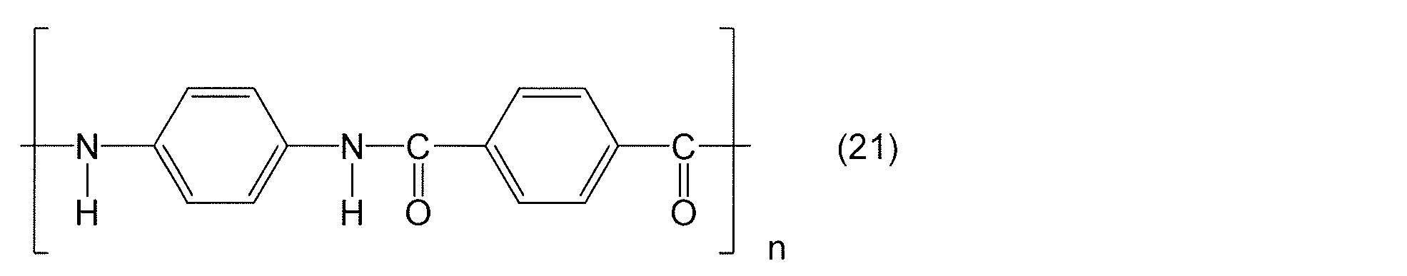


上記式(4)~(20)および(23)で表されるポリイミド系樹脂またはポリアミド系樹脂は、市販のものを用いても良い。上記ポリイミド系樹脂からなる基材の市販品としては、例えば、三菱ガス化学社製のネオプリム等が挙げられ、上記ポリアミド系樹脂からなる基材の市販品としては、例えば、東レ社製のミクトロン等が挙げられる。
Commercially available polyimide resins or polyamide resins represented by the above formulas (4) to (20) and (23) may be used. Examples of the commercially available base material made of the polyimide-based resin include Neoprim manufactured by Mitsubishi Gas Chemical Co., Ltd., and examples of the commercially available base material made of the polyamide-based resin include Mikutron manufactured by Toray Industries, Inc. Is mentioned.
また、上記式(4)~(20)および(23)で表されるポリイミド系樹脂またはポリアミド系樹脂は、公知の方法により合成したものを用いても良い。例えば、上記式(4)で表されるポリイミドフィルムの合成方法は、特開2009-132091に記載されており、具体的には、下記式(21)で表される4,4’-ヘキサフルオロプロピリデンビスフタル酸二無水物(FPA)と2,2’-ビス(トリフルオロメチル)-4,4’-ジアミノビフェニル(TFDB)とを反応させることにより得ることができる。

The polyimide resin or polyamide resin represented by the above formulas (4) to (20) and (23) may be synthesized by a known method. For example, a method for synthesizing a polyimide film represented by the above formula (4) is described in JP-A-2009-132091. Specifically, 4,4′-hexafluoro represented by the following formula (21) is described. It can be obtained by reacting propylidenebisphthalic dianhydride (FPA) with 2,2′-bis (trifluoromethyl) -4,4′-diaminobiphenyl (TFDB).
上記ポリイミド系樹脂又はポリアミド系樹脂の重量平均分子量は、3000以上50万以下の範囲であることが好ましく、5000~30万の範囲であることがより好ましく、1万以上20万以下の範囲であることが更に好ましい。重量平均分子量が3000未満であると、充分な強度が得られないことがあり、50万を超えると粘度が上昇し、溶解性が低下するため、表面が平滑で膜厚が均一な基材が得られないことがある。なお、本明細書において、「重量平均分子量」とは、ゲル浸透クロマトグラフィー(GPC)により測定したポリスチレン換算値である。
The weight average molecular weight of the polyimide resin or polyamide resin is preferably in the range of 3,000 to 500,000, more preferably in the range of 5,000 to 300,000, and in the range of 10,000 to 200,000. More preferably. When the weight average molecular weight is less than 3000, sufficient strength may not be obtained. When the weight average molecular weight exceeds 500,000, the viscosity increases and the solubility decreases, so that a substrate having a smooth surface and a uniform film thickness can be obtained. It may not be obtained. In the present specification, the “weight average molecular weight” is a polystyrene conversion value measured by gel permeation chromatography (GPC).
上記ポリイミド系樹脂およびポリアミド系樹脂のなかでも、優れた透明性を有することから、分子内又は分子間の電荷移動が起こりにくい構造を有するポリイミド基材またはポリアミド系樹脂が好ましく、具体的には、上記式(4)~(11)等のフッ素化ポリイミドフィルム、上記式(13)~(15)等の脂環構造を有するポリイミド系樹脂、上記式(23)等のハロゲン基を有するポリアミド系樹脂が挙げられる。
Among the polyimide resins and polyamide resins, a polyimide base material or polyamide resin having a structure in which charge transfer within a molecule or between molecules hardly occurs is preferable because it has excellent transparency. Specifically, Fluorinated polyimide films of the above formulas (4) to (11), polyimide resins having an alicyclic structure such as the above formulas (13) to (15), and polyamide resins having a halogen group such as the above formula (23) Is mentioned.
また、上記式(4)~(11)等のフッ素化ポリイミド系樹脂では、フッ素化された構造を有するため、高い耐熱性を有しており、ポリイミド系樹脂からなる基材の製造時の熱によって着色されることもないので、優れた透明性を有する。
In addition, the fluorinated polyimide resins such as the above formulas (4) to (11) have a fluorinated structure and thus have high heat resistance, and heat during the production of the substrate made of the polyimide resin. Since it is not colored by, it has the outstanding transparency.
基材11は、樹脂層12の表面12AにおけるJIS K5600-5-4:1999に規定される鉛筆硬度試験(荷重:750g、速度:1mm/秒)の条件で測定された硬度を、3H以上にできることが可能な観点から、上記式(4)~(11)等で表されるフッ素化ポリイミド系樹脂からなる基材又は上記式(23)等のハロゲン基を有するポリアミド系樹脂からなる基材を用いることが好ましい。なかでも、上記鉛筆硬度を3H以上の極めて優れた硬度を付与できることから、上記式(4)で表されるポリイミド系樹脂からなる基材を用いることがより好ましい。
The base material 11 has a hardness measured on the surface 12A of the resin layer 12 under the conditions of a pencil hardness test (load: 750 g, speed: 1 mm / second) specified in JIS K5600-5-4: 1999 of 3H or more. From a possible viewpoint, a base material composed of a fluorinated polyimide resin represented by the above formulas (4) to (11) or a base material composed of a polyamide resin having a halogen group such as the above formula (23) is used. It is preferable to use it. Especially, since the said pencil hardness can provide very excellent hardness of 3H or more, it is more preferable to use the base material which consists of a polyimide-type resin represented by the said Formula (4).
ポリエステル系樹脂としては、例えば、ポリエチレンテレフタレート、ポリプロピレンテレフタレート、ポリブチレンテレフタレート、ポリエチレンナフタレートの少なくとも1種を構成成分とする樹脂等が挙げられる。
Examples of the polyester-based resin include resins having at least one of polyethylene terephthalate, polypropylene terephthalate, polybutylene terephthalate, and polyethylene naphthalate as constituent components.
<<樹脂層>>
樹脂層12は、第1層から第n層(nは3以上の整数である)まで積層された多層構造のものである。第1層から第n層は、主として樹脂からなる層であることは言うまでもないが、樹脂の他に、粒子や添加剤等を含んでいてもよい。 << Resin layer >>
Theresin layer 12 has a multilayer structure in which layers from the first layer to the n-th layer (n is an integer of 3 or more) are stacked. Needless to say, the first to nth layers are layers mainly made of a resin, but may contain particles, additives and the like in addition to the resin.
樹脂層12は、第1層から第n層(nは3以上の整数である)まで積層された多層構造のものである。第1層から第n層は、主として樹脂からなる層であることは言うまでもないが、樹脂の他に、粒子や添加剤等を含んでいてもよい。 << Resin layer >>
The
樹脂層12における第1層~第n層のそれぞれのインデンテーション硬さは、第1層から第n層にかけて順に大きくなっている。すなわち、樹脂層12においては、第1層、第2層、…、第n層のインデンテーション硬さを、それぞれ、HIT1、HIT2、…、HITnとしたとき、以下の関係式(A)を満たしている。
HIT1<HIT2<…<HITn …(A) The indentation hardness of each of the first to nth layers in theresin layer 12 increases in order from the first layer to the nth layer. That is, in the resin layer 12, when the indentation hardness of the first layer, the second layer,..., The nth layer is H IT1 , H IT2 ,. ) Is satisfied.
H IT1 <H IT2 <... <H ITn (A)
HIT1<HIT2<…<HITn …(A) The indentation hardness of each of the first to nth layers in the
H IT1 <H IT2 <... <H ITn (A)
具体的には、樹脂層12は、第1層12Bから第3層12Dまで基材11側からこの順で積層された多層構造となっているので、第1層12B、第2層12C、第3層12Dのそれぞれのインデンテーション硬さは、第1層12Bから第3層12Dにかけて順に大きくなっている。すなわち、第1層12B、第2層12C、および第3層12Dのインデンテーション硬さを、それぞれ、HIT1、HIT2、HIT3としたとき、以下の関係式(B)を満たしている。
HIT1<HIT2<HIT3 …(B) Specifically, since theresin layer 12 has a multilayer structure in which the first layer 12B to the third layer 12D are laminated in this order from the substrate 11 side, the first layer 12B, the second layer 12C, The indentation hardness of each of the three layers 12D increases in order from the first layer 12B to the third layer 12D. That is, when the indentation hardness of the first layer 12B, the second layer 12C, and the third layer 12D is set to H IT1 , H IT2 and H IT3 , the following relational expression (B) is satisfied.
H IT1 <H IT2 <H IT3 (B)
HIT1<HIT2<HIT3 …(B) Specifically, since the
H IT1 <H IT2 <H IT3 (B)
本明細書において、「インデンテーション硬さ」とは、ナノインデンテーション法による硬度測定により、各樹脂層に圧子を100nm押込んだときの硬度である。上記ナノインデンテーション法によるインデンテーション硬さの測定は、HYSITRON(ハイジトロン)社製の「TI950 TriboIndenter」を用いて行うものとする。具体的には、まず、1mm×10mmに切り出した光学フィルムを包埋樹脂によって包埋したブロックを作製し、このブロックから一般的な切片作製方法によって穴等がない均一な、厚さ70nm以上100nm以下の切片を切り出す。切片の作製には、「ウルトラミクロトーム EM UC7」(ライカ マイクロシステムズ株式会社)等を用いることができる。そして、この穴等がない均一な切片が切り出された残りのブロックを測定サンプルとする。次いで、このような測定サンプルにおける上記切片が切り出されることによって得られた各樹脂層の断面中央において、上記圧子としてBerkovich圧子(三角錐)を最大荷重40μN、速度10μN/sで約100nm押し込み、一定保持して残留応力の緩和を行った後、除荷させて、緩和後の最大荷重を計測し、該最大荷重(Pmax(μN))と、圧子と試料(各層)との接触投影面積(Ap(nm2))とを用い、Pmax/Apにより、インデンテーション硬さを算出する。インデンテーション硬さは、10回測定した値の算術平均値とする。
In the present specification, the “indentation hardness” is the hardness when an indenter is pressed 100 nm into each resin layer by the hardness measurement by the nanoindentation method. The measurement of the indentation hardness by the nanoindentation method is performed using “TI950 TriboIndenter” manufactured by HYSITRON. Specifically, first, a block in which an optical film cut out to 1 mm × 10 mm is embedded with an embedding resin is prepared, and a uniform thickness without a hole or the like is obtained from this block by a general section manufacturing method. Cut the following sections. “Ultramicrotome EM UC7” (Leica Microsystems) can be used for preparing the slice. The remaining block from which a uniform section without holes or the like is cut out is taken as a measurement sample. Next, at the center of the cross section of each resin layer obtained by cutting out the section in such a measurement sample, a Berkovich indenter (triangular pyramid) is pushed in as a indenter about 100 nm at a maximum load of 40 μN and a speed of 10 μN / s, and constant. After holding and relaxing the residual stress, unloading and measuring the maximum load after relaxation, the maximum load (P max (μN)) and the projected contact area between the indenter and the sample (each layer) ( Indentation hardness is calculated from P max / A p using A p (nm 2 )). The indentation hardness is the arithmetic average value of the values measured 10 times.
光学フィルム10においては、樹脂層12は、第1層12B、第2層12C、および第3層12Dから構成されているので、上記nが3であるが、上記第n層のnは、3以上であれば特に限定されない。上記nの上限は、生産性の観点から、10以下であることが好ましい。
In the optical film 10, since the resin layer 12 is composed of the first layer 12B, the second layer 12C, and the third layer 12D, the n is 3, but the n of the n-th layer is 3 If it is more, it will not specifically limit. The upper limit of n is preferably 10 or less from the viewpoint of productivity.
樹脂層12が3層構造の場合、第1層12B、第2層12C、第3層12Dの各インデンテーション硬さは、上記関係式(B)を満たしていれば、特に限定されないが、第1層12Bのインデンテーション硬さは、1MPa以上100MPa以下となっており、第2層12Cのインデンテーション硬さは、10MPa以上500MPa以下となっており、第3層12Dのインデンテーション硬さは、100MPa以上1000MPa以下となっていることが好ましい。第1層のインデンテーション硬さが、1MPa以上であると、鉛筆硬度をより向上させることができ、また第1層のインデンテーション硬さが、100MPa以下であると、耐衝撃性をより向上させることができる。第2層のインデンテーション硬さが、10MPa以上であると、光学フィルムを折り畳んだ際に樹脂層の割れがより発生しにくくなり、また第2層のインデンテーション硬さが、500MPa以下であると、光学フィルムを折り畳んだ際に樹脂層のシワがより発生しにくくなる。第3層のインデンテーション硬さが、100MPa以上であると、耐擦傷性をより向上させることができ、また第3層のインデンテーション硬さが、1000MPa以下であると、光学フィルムを折り畳んだ際に樹脂層の割れがより発生しにくくなる。
When the resin layer 12 has a three-layer structure, each indentation hardness of the first layer 12B, the second layer 12C, and the third layer 12D is not particularly limited as long as the relational expression (B) is satisfied. The indentation hardness of the first layer 12B is 1 MPa or more and 100 MPa or less, the indentation hardness of the second layer 12C is 10 MPa or more and 500 MPa or less, and the indentation hardness of the third layer 12D is It is preferably 100 MPa or more and 1000 MPa or less. When the indentation hardness of the first layer is 1 MPa or more, the pencil hardness can be further improved, and when the indentation hardness of the first layer is 100 MPa or less, the impact resistance is further improved. be able to. When the indentation hardness of the second layer is 10 MPa or more, cracking of the resin layer is less likely to occur when the optical film is folded, and the indentation hardness of the second layer is 500 MPa or less. When the optical film is folded, wrinkles of the resin layer are less likely to occur. When the indentation hardness of the third layer is 100 MPa or more, the scratch resistance can be further improved, and when the indentation hardness of the third layer is 1000 MPa or less, the optical film is folded. In addition, cracks in the resin layer are less likely to occur.
<第1層>
第1層12Bは、第1層12Bから第3層12Dのうち最も低いインデンテーション硬さを有する層であり、主に、鉛筆硬度および耐衝撃性を向上させる機能を有する。第1層12Bの膜厚は、50μm以上300μm以下となっていることが好ましい。第1層の膜厚が、50μm以上であると、樹脂層の硬度をより向上させることができ、また300μm以下であると、膜厚が厚すぎず、薄型化に適しているとともに、加工性も良好である。第1層12Bの膜厚は、走査型電子顕微鏡(SEM)を用いて、第1層12Bの断面を撮影し、その断面の画像において第1層12Bの膜厚を20箇所測定し、その20箇所の膜厚の算術平均値とする。第1層12Bの下限は80μm以上、100μm以上、150μm以上の順にさらに好ましく(数値が大きいほど好ましい)、第1層12Bの上限は250μm以下、220μm以下、200μm以下の順にさらに好ましい(数値が小さいほど好ましい)。 <First layer>
Thefirst layer 12B is a layer having the lowest indentation hardness among the first layer 12B to the third layer 12D, and mainly has a function of improving pencil hardness and impact resistance. The film thickness of the first layer 12B is preferably 50 μm or more and 300 μm or less. When the film thickness of the first layer is 50 μm or more, the hardness of the resin layer can be further improved. When the film thickness is 300 μm or less, the film thickness is not too thick and is suitable for thinning, and processability is improved. Is also good. The film thickness of the first layer 12B is obtained by photographing a cross section of the first layer 12B using a scanning electron microscope (SEM), measuring the film thickness of the first layer 12B in 20 positions in the image of the cross section, The arithmetic average value of the film thickness at the location is used. The lower limit of the first layer 12B is more preferably in the order of 80 μm or more, 100 μm or more, and 150 μm or more (higher values are preferable), and the upper limit of the first layer 12B is more preferable in the order of 250 μm or less, 220 μm or less, 200 μm or less. Is preferable).
第1層12Bは、第1層12Bから第3層12Dのうち最も低いインデンテーション硬さを有する層であり、主に、鉛筆硬度および耐衝撃性を向上させる機能を有する。第1層12Bの膜厚は、50μm以上300μm以下となっていることが好ましい。第1層の膜厚が、50μm以上であると、樹脂層の硬度をより向上させることができ、また300μm以下であると、膜厚が厚すぎず、薄型化に適しているとともに、加工性も良好である。第1層12Bの膜厚は、走査型電子顕微鏡(SEM)を用いて、第1層12Bの断面を撮影し、その断面の画像において第1層12Bの膜厚を20箇所測定し、その20箇所の膜厚の算術平均値とする。第1層12Bの下限は80μm以上、100μm以上、150μm以上の順にさらに好ましく(数値が大きいほど好ましい)、第1層12Bの上限は250μm以下、220μm以下、200μm以下の順にさらに好ましい(数値が小さいほど好ましい)。 <First layer>
The
上記第1層の膜厚は、走査型電子顕微鏡(SEM)を用いて、第1層の断面を撮影し、その断面の画像において第1層の膜厚を20箇所測定し、その20箇所の膜厚の算術平均値とする。具体的な断面写真の撮影方法を以下に記載する。まず、1mm×10mmに切り出した光学フィルムを包埋樹脂によって包埋したブロックを作製し、このブロックから一般的な切片作製方法によって穴等がない均一な、厚さ70nm以上100nm以下の切片を切り出す。切片の作製には、「ウルトラミクロトーム EM UC7」(ライカ マイクロシステムズ株式会社)等を用いることができる。そして、この穴等がない均一な切片が切り出された残りのブロックを測定サンプルとする。その後、走査型電子顕微鏡(SEM)(製品名「S-4800」、日立ハイテクノロジーズ社製)を用いて、測定サンプルの断面写真を撮影する。上記S-4800を用いて断面写真を撮影する際には、検出器を「SE」、加速電圧を「5kV」、エミッション電流を「10μA」にして断面観察を行う。倍率については、フォーカスを調節しコントラストおよび明るさを各層が見分けられるか観察しながら100~10万倍で適宜調節する。なお、上記S-4800を用いて断面写真を撮影する際には、さらに、アパーチャーを「ビームモニタ絞り3」にし、対物レンズ絞りを「3」にし、またW.D.を「8mm」にしてもよい。第1層の膜厚を測定する際には、断面観察した折に、第1層と他の層(例えば、第2層)との界面コントラストが可能な限り明確に観察できることが重要となる。仮に、コントラスト不足でこの界面が見え難い場合には、四酸化オスミウム、四酸化ルテニウム、リンタングステン酸など染色処理を施すと、有機層間の界面が見やすくなるので、染色処理を行ってもよい。また、界面のコントラストは高倍率である方が分かりにくい場合がある。その場合には、低倍率も同時に観察する。例えば、2.5万倍と5万倍や、5万倍と10万倍など、高低の2つの倍率で観察し、両倍率で上記した算術平均値を求め、さらにその平均値を第1層の膜厚の値とする。
The film thickness of the first layer is obtained by photographing a cross section of the first layer using a scanning electron microscope (SEM), measuring 20 film thicknesses of the first layer in the image of the cross section, The arithmetic average value of the film thickness is used. A specific method for taking a cross-sectional photograph is described below. First, a block is prepared by embedding an optical film cut into 1 mm × 10 mm with an embedding resin, and a uniform section having a thickness of 70 nm or more and 100 nm or less without holes is cut out from this block by a general section preparation method. . For the preparation of the section, “Ultra Microtome EM UC7” (Leica Microsystems Co., Ltd.) or the like can be used. The remaining block from which a uniform section without holes or the like is cut out is taken as a measurement sample. Thereafter, a cross-sectional photograph of the measurement sample is taken using a scanning electron microscope (SEM) (product name “S-4800”, manufactured by Hitachi High-Technologies Corporation). When taking a cross-sectional photograph using the S-4800, the cross-section is observed with the detector set to “SE”, the acceleration voltage set to “5 kV”, and the emission current set to “10 μA”. The magnification is appropriately adjusted from 100 to 100,000 times while adjusting the focus and observing whether each layer can be distinguished. When taking a cross-sectional photograph using the above S-4800, the aperture is set to “beam monitor aperture 3”, the objective lens aperture is set to “3”, and the W.S. D. May be set to “8 mm”. When measuring the thickness of the first layer, it is important that the interface contrast between the first layer and another layer (for example, the second layer) can be observed as clearly as possible when the cross-section is observed. If it is difficult to see this interface due to insufficient contrast, a dyeing process such as osmium tetroxide, ruthenium tetroxide, or phosphotungstic acid can be used to easily see the interface between the organic layers. Also, the interface contrast may be difficult to understand when the magnification is high. In that case, the low magnification is also observed at the same time. For example, observe at two magnifications of high and low, such as 25,000 times and 50,000 times, and 50,000 times and 100,000 times, and obtain the arithmetic average value described above at both magnifications. The value of the film thickness.
第1層12Bを構成する樹脂は、第1層12Bのインデンテーション硬さが第2層12Cのインデンテーション硬さよりも低くなるような樹脂であれば、特に限定されない。このような樹脂としては、例えば、ウレタン系樹脂、エポキシ系樹脂、シリコーン系樹脂等が挙げられる。これらの中でも、ウレタン系樹脂は、靱性に優れているので、優れた折り畳み性能を得る観点および鉛筆硬度が3H以上となる優れた硬度を得る観点から、ウレタン系樹脂が好ましい。なお、樹脂層12は、ウレタン系樹脂やエポキシ系樹脂等の他、ゴムや熱可塑性エラストマーを含有していてもよい。
The resin constituting the first layer 12B is not particularly limited as long as the indentation hardness of the first layer 12B is lower than the indentation hardness of the second layer 12C. Examples of such a resin include urethane resins, epoxy resins, silicone resins, and the like. Among these, since the urethane-based resin is excellent in toughness, the urethane-based resin is preferable from the viewpoint of obtaining excellent folding performance and obtaining excellent hardness with a pencil hardness of 3H or more. In addition, the resin layer 12 may contain rubber | gum and a thermoplastic elastomer other than urethane type resin, an epoxy resin, etc.
ウレタン系樹脂は、ウレタン結合を有する樹脂である。ウレタン系樹脂としては、電離放射線硬化性ウレタン系樹脂組成物の硬化物や熱硬化性ウレタン系樹脂組成物の硬化物等が挙げられる。これらの中でも、耐擦傷性および高硬度が得られ、また硬化速度も早く量産性に優れる観点から、電離放射線硬化性ウレタン系樹脂組成物の硬化物であることが好ましい。
Urethane resin is a resin having a urethane bond. Examples of the urethane resin include a cured product of an ionizing radiation curable urethane resin composition and a cured product of a thermosetting urethane resin composition. Among these, a cured product of an ionizing radiation-curable urethane-based resin composition is preferable from the viewpoint that scratch resistance and high hardness are obtained, and the curing rate is high and the mass productivity is excellent.
電離放射線硬化性ウレタン系樹脂組成物は、ウレタン(メタ)アクリレートを含んでおり、熱硬化性ウレタン系樹脂組成物は、ポリオール化合物と、イソシアネート化合物とを含んでいる。ウレタン(メタ)アクリレート、ポリオール化合物、およびイソシアネート化合物は、モノマー、オリゴマー、およびプレポリマーのいずれであってもよい。なお、「ウレタン(メタ)アクリレート」とは、「ウレタンアクリレート」および「ウレタンメタクリレート」の両方を含む意味である。
The ionizing radiation curable urethane resin composition contains urethane (meth) acrylate, and the thermosetting urethane resin composition contains a polyol compound and an isocyanate compound. The urethane (meth) acrylate, polyol compound, and isocyanate compound may be any of a monomer, an oligomer, and a prepolymer. The “urethane (meth) acrylate” means both “urethane acrylate” and “urethane methacrylate”.
ウレタン(メタ)アクリレート中の(メタ)アクリロイル基の数(官能基数)は、2以上6以下であることが好ましい。ウレタン(メタ)アクリレート中の(メタ)アクリロイル基の数が、2未満であると、鉛筆硬度が低くなるおそれがあり、また6を超えると、硬化収縮が大きくなり、光学フィルムがカールしてしまい、また折り曲げ時に樹脂層にクラックが入るおそれがある。ウレタン(メタ)アクリレート中の(メタ)アクリロイル基の数の上限は、3以下であることがより好ましい。なお、「(メタ)アクリロイル基」とは、「アクリロイル基」および「メタクリロイル基」の両方を含む意味である。
The number (functional group number) of (meth) acryloyl groups in urethane (meth) acrylate is preferably 2 or more and 6 or less. If the number of (meth) acryloyl groups in the urethane (meth) acrylate is less than 2, the pencil hardness may be low, and if it exceeds 6, the curing shrinkage increases and the optical film curls. In addition, there is a risk of cracks in the resin layer during bending. The upper limit of the number of (meth) acryloyl groups in the urethane (meth) acrylate is more preferably 3 or less. The “(meth) acryloyl group” means to include both “acryloyl group” and “methacryloyl group”.
ウレタン(メタ)アクリレートの重量平均分子量は、特に限定されないが、1500以上20000以下であることが好ましい。ウレタン(メタ)アクリレートの重量平均分子量が、1500未満であると、耐衝撃性が低下するおそれがあり、また20000を超えると、電離放射線硬化性ウレタン系樹脂組成物の粘度が上昇し、塗工性が悪化するおそれがある。ウレタン(メタ)アクリレートの重量平均分子量の下限は2000以上であることがより好ましく、上限は15000以下であることがより好ましい。
The weight average molecular weight of urethane (meth) acrylate is not particularly limited, but is preferably 1500 or more and 20000 or less. If the weight average molecular weight of the urethane (meth) acrylate is less than 1500, the impact resistance may be lowered. If it exceeds 20000, the viscosity of the ionizing radiation-curable urethane resin composition increases, and the coating is applied. May deteriorate. The lower limit of the weight average molecular weight of the urethane (meth) acrylate is more preferably 2000 or more, and the upper limit is more preferably 15000 or less.
また、ウレタン(メタ)アクリレート由来の構造を有する繰り返し単位としては、例えば、下記一般式(25)、(26)、(27)または(28)で表される構造等が挙げられる。

上記一般式(25)中、R7は分岐鎖状アルキル基を示し、R8は分岐鎖状アルキル基又は飽和環状脂肪族基を示し、R9は水素原子又はメチル基を示し、R10は、水素原子、メチル基又はエチル基を示し、mは0以上の整数を示し、xは0~3の整数を示す。
Moreover, as a repeating unit which has a structure derived from urethane (meth) acrylate, the structure etc. which are represented by the following general formula (25), (26), (27) or (28) are mentioned, for example.
In the general formula (25), R 7 represents a branched alkyl group, R 8 represents a branched alkyl group or a saturated cycloaliphatic group, R 9 represents a hydrogen atom or a methyl group, and R 10 represents , A hydrogen atom, a methyl group or an ethyl group, m represents an integer of 0 or more, and x represents an integer of 0 to 3.


なお、第1層12B等を構成する樹脂が、どのような構造の高分子鎖(繰り返し単位)によって形成されているかは、例えば、熱分解GC-MS及びFT-IRによって第1層12B等を分析することによって判断可能である。特に、熱分解GC-MSは、第1層12B等に含まれる単量体単位をモノマー成分として検知できるため有用である。
The structure of the resin constituting the first layer 12B and the like is defined by the structure of the polymer chain (repeating unit) by, for example, the first layer 12B and the like by pyrolysis GC-MS and FT-IR. Judgment can be made by analysis. In particular, pyrolysis GC-MS is useful because it can detect monomer units contained in the first layer 12B and the like as monomer components.
第1層12Bは、インデンテーション硬さが、第2層12Cのインデンテーション硬さよりも低ければ、Hz紫外線吸収剤、分光透過率調整剤等を含んでいてもよい。
If the indentation hardness is lower than the indentation hardness of the second layer 12C, the first layer 12B may contain a Hz ultraviolet absorber, a spectral transmittance adjusting agent, and the like.
<紫外線吸収剤>
光学フィルムは、折り畳み可能なスマートフォンやタブレット端末のようなモバイル端末に特に好適に用いられるが、このようなモバイル端末は屋外で使用されることが多く、そのため、光学フィルムより表示素子側に配置された偏光子が紫外線に晒されて劣化しやすいという問題がある。しかしながら、第1層は、偏光子の表示画面側に配置されるため、第1層に紫外吸収剤が含有されていると、偏光子が紫外線に晒されることによる劣化を好適に防止することができる。なお、上記紫外線吸収剤(UVA)は、基材11や第2層~第n層の少なくともいずれかに含有されていてもよい。この場合、紫外線吸収剤(UVA)は、第1層12Bに含有されていなくてもよい。 <Ultraviolet absorber>
The optical film is particularly preferably used for a mobile terminal such as a foldable smartphone or tablet terminal. However, such a mobile terminal is often used outdoors, and therefore, the optical film is disposed closer to the display element than the optical film. There is a problem that the polarizer is easily deteriorated by being exposed to ultraviolet rays. However, since the first layer is disposed on the display screen side of the polarizer, if the ultraviolet absorber is contained in the first layer, deterioration due to exposure of the polarizer to ultraviolet rays can be suitably prevented. it can. The ultraviolet absorbent (UVA) may be contained in at least one of thebase material 11 and the second to nth layers. In this case, the ultraviolet absorber (UVA) may not be contained in the first layer 12B.
光学フィルムは、折り畳み可能なスマートフォンやタブレット端末のようなモバイル端末に特に好適に用いられるが、このようなモバイル端末は屋外で使用されることが多く、そのため、光学フィルムより表示素子側に配置された偏光子が紫外線に晒されて劣化しやすいという問題がある。しかしながら、第1層は、偏光子の表示画面側に配置されるため、第1層に紫外吸収剤が含有されていると、偏光子が紫外線に晒されることによる劣化を好適に防止することができる。なお、上記紫外線吸収剤(UVA)は、基材11や第2層~第n層の少なくともいずれかに含有されていてもよい。この場合、紫外線吸収剤(UVA)は、第1層12Bに含有されていなくてもよい。 <Ultraviolet absorber>
The optical film is particularly preferably used for a mobile terminal such as a foldable smartphone or tablet terminal. However, such a mobile terminal is often used outdoors, and therefore, the optical film is disposed closer to the display element than the optical film. There is a problem that the polarizer is easily deteriorated by being exposed to ultraviolet rays. However, since the first layer is disposed on the display screen side of the polarizer, if the ultraviolet absorber is contained in the first layer, deterioration due to exposure of the polarizer to ultraviolet rays can be suitably prevented. it can. The ultraviolet absorbent (UVA) may be contained in at least one of the
紫外線吸収剤としては、例えば、トリアジン系紫外線吸収剤、ベンゾフェノン系紫外線吸収剤、及び、ベンゾトリアゾール系紫外線吸収剤等が挙げられる。
Examples of ultraviolet absorbers include triazine-based ultraviolet absorbers, benzophenone-based ultraviolet absorbers, and benzotriazole-based ultraviolet absorbers.
上記トリアジン系紫外線吸収剤としては、例えば、2-(2-ヒドロキシ-4-[1-オクチルオキシカルボニルエトキシ]フェニル)-4,6-ビス(4-フェニルフェニル)-1,3,5-トリアジン、2-[4-[(2-ヒドロキシ-3-ドデシルオキシプロピル)オキシ]-2-ヒドロキシフェニル]-4,6-ビス(2,4-ジメチルフェニル)-1,3,5-トリアジン、2,4-ビス[2-ヒドロキシ-4-ブトキシフェニル]-6-(2,4-ジブトキシフェニル)-1,3,5-トリアジン、2-[4-[(2-ヒドロキシ-3-トリデシルオキシプロピル)オキシ]-2-ヒドロキシフェニル]-4,6-ビス(2,4-ジメチルフェニル)-1,3,5-トリアジン、および2-[4-[(2-ヒドロキシ-3-(2’-エチル)ヘキシル)オキシ]-2-ヒドロキシフェニル]-4,6-ビス(2,4-ジメチルフェニル)-1,3,5-トリアジン等が挙げられる。市販されているトリアジン系紫外線吸収剤としては、例えば、TINUVIN460、TINUVIN477(いずれも、BASF社製)、LA-46(ADEKA社製)等が挙げられる。
Examples of the triazine ultraviolet absorber include 2- (2-hydroxy-4- [1-octyloxycarbonylethoxy] phenyl) -4,6-bis (4-phenylphenyl) -1,3,5-triazine. 2- [4-[(2-hydroxy-3-dodecyloxypropyl) oxy] -2-hydroxyphenyl] -4,6-bis (2,4-dimethylphenyl) -1,3,5-triazine, 2 , 4-Bis [2-hydroxy-4-butoxyphenyl] -6- (2,4-dibutoxyphenyl) -1,3,5-triazine, 2- [4-[(2-hydroxy-3-tridecyl) Oxypropyl) oxy] -2-hydroxyphenyl] -4,6-bis (2,4-dimethylphenyl) -1,3,5-triazine, and 2- [4-[(2-hydroxy-3- ( '- ethyl) hexyl) oxy] -2-hydroxyphenyl] -4,6-bis (2,4-dimethylphenyl) -1,3,5-triazine. Examples of commercially available triazine ultraviolet absorbers include TINUVIN 460, TINUVIN 477 (both manufactured by BASF), LA-46 (manufactured by ADEKA), and the like.
上記ベンゾフェノン系紫外線吸収剤としては、例えば、2-ヒドロキシベンゾフェノン、2,4-ジヒドロキシベンゾフェノン、2,2’-ジヒドロキシ-4,4’-ジメトキシベンゾフェノン、2,2’,4,4’-テトラヒドロキシベンゾフェノン、2-ヒドロキシ-4-メトキシベンゾフェノン、ヒドロキシメトキシベンゾフェノンスルホン酸及びその三水塩、ヒドロキシメトキシベンゾフェノンスルホン酸ナトリウム等が挙げられる。市販されているベンゾフェノン系紫外線吸収剤としては、例えば、CHMASSORB81/FL(BASF社製)等が挙げられる。
Examples of the benzophenone ultraviolet absorber include 2-hydroxybenzophenone, 2,4-dihydroxybenzophenone, 2,2′-dihydroxy-4,4′-dimethoxybenzophenone, 2,2 ′, 4,4′-tetrahydroxy. Examples thereof include benzophenone, 2-hydroxy-4-methoxybenzophenone, hydroxymethoxybenzophenone sulfonic acid and its trihydrate, hydroxymethoxybenzophenone sulfonate sodium, and the like. Examples of commercially available benzophenone ultraviolet absorbers include CHMASSORB81 / FL (manufactured by BASF).
上記ベンゾトリアゾール系紫外線吸収剤としては、例えば、2-エチルヘキシル-3-〔3-tert-ブチル-4-ヒドロキシ-5-(5-クロロ-2H-ベンゾトリアゾール-2-イル)フェニル〕プロピオネート、2-(2H-ベンゾトリアゾール-2-イル)-6-(直鎖及び側鎖ドデシル)-4-メチルフェノール、2-〔5-クロロ(2H)-ベンゾトリアゾール-2-イル〕-4-メチル-6-(tert-ブチル)フェノール、2-(2H-ベンゾトリアゾール-2-イル)-4,6-ジ-tert-ペンチルフェノール、2-(2’-ヒドロキシ-5’-メチルフェニル)ベンゾトリアゾール、2-(2’-ヒドロキシ-3’,5’-ジ-tert-ブチルフェニル)ベンゾトリアゾール、2-(2’-ヒドロキシ-3’-tert-ブチル-5’-メチルフェニル)ベンゾトリアゾール、2-(2’-ヒドロキシ-3’,5’-ジ-tert-ブチルフェニル)-5-クロロベンゾトリアゾール、2-(2’-ヒドロキシ-3’-(3’’,4’’,5’’,6’’-テトラヒドロフタルイミドメチル)-5’-メチルフェニル)ベンゾトリアゾール、2,2-メチレンビス(4-(1,1,3,3-テトラメチルブチル)-6-(2H-ベンゾトリアゾール-2-イル)フェノール)、及び、2-(2’-ヒドロキシ-3′-tert-ブチル-5′-メチルフェニル)-5-クロロベンゾトリアゾール等が挙げられる。市販されているベンゾトリアゾール系紫外線吸収剤としては、例えば、KEMISORB71D、KEMISORB79(いずれも、ケミプロ化成社製)、JF-80、JAST-500(いずれも、城北化学社製)、ULS-1933D(一方社製)、RUVA-93(大塚化学社製)等が挙げられる。
Examples of the benzotriazole ultraviolet absorber include 2-ethylhexyl-3- [3-tert-butyl-4-hydroxy-5- (5-chloro-2H-benzotriazol-2-yl) phenyl] propionate, 2 -(2H-benzotriazol-2-yl) -6- (linear and side chain dodecyl) -4-methylphenol, 2- [5-chloro (2H) -benzotriazol-2-yl] -4-methyl- 6- (tert-butyl) phenol, 2- (2H-benzotriazol-2-yl) -4,6-di-tert-pentylphenol, 2- (2′-hydroxy-5′-methylphenyl) benzotriazole, 2- (2′-hydroxy-3 ′, 5′-di-tert-butylphenyl) benzotriazole, 2- (2′-hydroxy-3) -Tert-butyl-5'-methylphenyl) benzotriazole, 2- (2'-hydroxy-3 ', 5'-di-tert-butylphenyl) -5-chlorobenzotriazole, 2- (2'-hydroxy- 3 ′-(3 ″, 4 ″, 5 ″, 6 ″ -tetrahydrophthalimidomethyl) -5′-methylphenyl) benzotriazole, 2,2-methylenebis (4- (1,1,3,3 -Tetramethylbutyl) -6- (2H-benzotriazol-2-yl) phenol) and 2- (2'-hydroxy-3'-tert-butyl-5'-methylphenyl) -5-chlorobenzotriazole Etc. Examples of commercially available benzotriazole ultraviolet absorbers include KEMISORB71D, KEMISORB79 (all manufactured by Chemipro Kasei Co., Ltd.), JF-80, JAST-500 (all manufactured by Johoku Chemical Co., Ltd.), ULS-1933D (one side) And RUVA-93 (manufactured by Otsuka Chemical Co., Ltd.).
紫外線吸収剤は、なかでも、トリアジン系紫外線吸収剤、ベンゾトリアゾール系紫外線吸収剤が好適に用いられる。紫外線吸収剤は、樹脂層を構成する樹脂成分との溶解性が高いほうが好ましく、また、上述した耐久折り畳み試験後のブリードアウトが少ないほうが好ましい。紫外線吸収剤は、ポリマー化又はオリゴマー化されていることが好ましい。紫外線吸収剤としては、ベンゾトリアゾール、トリアジン、ベンゾフェノン骨格を有するポリマー又はオリゴマーが好ましく、具体的には、ベンゾトリアゾールやベンゾフェノン骨格を有する(メタ)アクリレートと、メチルメタクリレート(MMA)とを任意の比率で熱共重合したものであることが好ましい。なお、有機発光ダイオード(OLED)表示装置に光学フィルムを適用する場合、紫外線吸収剤は、OLEDを紫外線から保護する役割も果たすことができる。
Among these, triazine ultraviolet absorbers and benzotriazole ultraviolet absorbers are preferably used as the ultraviolet absorber. It is preferable that the ultraviolet absorber has high solubility with the resin component constituting the resin layer, and it is preferable that the bleed-out after the above-described durability folding test is small. The ultraviolet absorber is preferably polymerized or oligomerized. As the ultraviolet absorber, a polymer or oligomer having a benzotriazole, triazine, or benzophenone skeleton is preferable. Specifically, (meth) acrylate having a benzotriazole or benzophenone skeleton and methyl methacrylate (MMA) at an arbitrary ratio. It is preferable that it has been heat copolymerized. In addition, when an optical film is applied to an organic light emitting diode (OLED) display device, the ultraviolet absorber can also serve to protect the OLED from ultraviolet rays.
紫外線吸収剤の含有量としては特に限定されないが、第1層用組成物の固形分100質量部に対して1質量部以上6質量部以下であることが好ましい。1質量部未満であると、上述した紫外線吸収剤を第1層に含有させる効果を充分に得ることができないことがあり、6質量部を超えると、第1層に著しい着色や強度低下が生じることがある。上記紫外線吸収剤の含有量のより好ましい下限は2質量部以上、より好ましい上限は5質量部以下である。
Although it does not specifically limit as content of a ultraviolet absorber, It is preferable that they are 1 mass part or more and 6 mass parts or less with respect to 100 mass parts of solid content of the composition for 1st layers. If the amount is less than 1 part by mass, the effect of containing the above-described ultraviolet absorber in the first layer may not be sufficiently obtained. Sometimes. The minimum with more preferable content of the said ultraviolet absorber is 2 mass parts or more, and a more preferable upper limit is 5 mass parts or less.
<分光透過率調整剤>
分光透過率調整剤は、光学フィルムの分光透過率を調整するものである。第1層に、例えば、下記一般式(29)で表されるセサモール型ベンゾトリアゾール系単量体を含ませた場合には、上述した分光透過率を好適に満たすことができる。

式中、R11は水素原子又はメチル基を表す。R12は炭素数1~6の直鎖状又は枝分かれ鎖状のアルキレン基又は炭素数1~6の直鎖状または分岐鎖状のオキシアルキレン基を表す。
<Spectral transmittance adjusting agent>
The spectral transmittance adjusting agent adjusts the spectral transmittance of the optical film. For example, when the sesamol type benzotriazole monomer represented by the following general formula (29) is included in the first layer, the above-described spectral transmittance can be preferably satisfied.
In the formula, R 11 represents a hydrogen atom or a methyl group. R 12 represents a linear or branched alkylene group having 1 to 6 carbon atoms or a linear or branched oxyalkylene group having 1 to 6 carbon atoms.
分光透過率調整剤は、光学フィルムの分光透過率を調整するものである。第1層に、例えば、下記一般式(29)で表されるセサモール型ベンゾトリアゾール系単量体を含ませた場合には、上述した分光透過率を好適に満たすことができる。
The spectral transmittance adjusting agent adjusts the spectral transmittance of the optical film. For example, when the sesamol type benzotriazole monomer represented by the following general formula (29) is included in the first layer, the above-described spectral transmittance can be preferably satisfied.
上記のセサモール型ベンゾトリアゾール系単量体としては特に制限されないが、具体的な物質名としては、2-[2-(6-ヒドロキシベンゾ[1,3]ジオキソール-5-イル)-2H-ベンゾトリアゾール-5-イル]エチルメタクリレート、2-[2-(6-ヒドロキシベンゾ[1,3]ジオキソール-5-イル)-2H-ベンゾトリアゾール-5-イル]エチルアクリレート、3-[2-(6-ヒドロキシベンゾ[1,3]ジオキソール-5-イル)-2H-ベンゾトリアゾール-5-イル]プロピルメタクリレート、3-[2-(6-ヒドロキシベンゾ[1,3]ジオキソール-5-イル)-2H-ベンゾトリアゾール-5-イル]プロピルアクリレート、4-[2-(6-ヒドロキシベンゾ[1,3]ジオキソール-5-イル)-2H-ベンゾトリアゾール-5-イル]ブチルメタクリレート、4-[2-(6-ヒドロキシベンゾ[1,3]ジオキソール-5-イル)-2H-ベンゾトリアゾール-5-イル]ブチルアクリレート、2-[2-(6-ヒドロキシベンゾ[1,3]ジオキソール-5-イル)-2H-ベンゾトリアゾール-5-イルオキシ]エチルメタクリレート、2-[2-(6-ヒドロキシベンゾ[1,3]ジオキソール-5-イル)-2H-ベンゾトリアゾール-5-イルオキシ]エチルアクリレート、2-[3-{2-(6-ヒドロキシベンゾ[1,3]ジオキソール-5-イル)-2H-ベンゾトリアゾール-5-イル}プロパノイルオキシ]エチルメタクリレート、2-[3-{2-(6-ヒドロキシベンゾ[1,3]ジオキソール-5-イル)-2H-ベンゾトリアゾール-5-イル}プロパノイルオキシ]エチルアクリレート、4-[3-{2-(6-ヒドロキシベンゾ[1,3]ジオキソール-5-イル)-2H-ベンゾトリアゾール-5-イル}プロパノイルオキシ]ブチルメタクリレート、4-[3-{ 2 -(6-ヒドロキシベンゾ[1,3]ジオキソール-5-イル)-2H-ベンゾトリアゾール-5-イル}プロパノイルオキシ]ブチルアクリレート、2-[3-{2-(6-ヒドロキシベンゾ[1,3]ジオキソール-5-イル)-2H-ベンゾトリアゾール-5-イル}プロパノイルオキシ]エチルメタクリレート、2-[3-{2-(6-ヒドロキシベンゾ[1,3]ジオキソール-5-イル)-2H-ベンゾトリアゾール-5-イル}プロパノイルオキシ]エチルアクリレート、2-(メタクリロイルオキシ)エチル2-(6-ヒドロキシベンゾ[1,3]ジオキソール-5-イル)-2H-ベンゾトリアゾール-5カルボキシレート、2-(アクリロイルオキシ)エチル2-(6-ヒドロキシベンゾ[1,3]ジオキソール-5-イル)-2H-ベンゾトリアゾール-5-カルボキシレート、4-(メタクリロイルオキシ)ブチル2-(6-ヒドロキシベンゾ[1,3]ジオキソール-5-イル)-2H-ベンゾトリアゾール-5-カルボキシレート、4-(アクリロイルオキシ)ブチル2-(6-ヒドロキシベンゾ[1,3]ジオキソール-5-イル)-2H-ベンゾトリアゾール-5-カルボキシレート等を挙げることができる。また、これらセサモール型ベンゾトリアゾール系単量体は1種類で用いてもよいし、また2種類以上用いてもよい。
The sesamol type benzotriazole monomer is not particularly limited, but specific substance names include 2- [2- (6-hydroxybenzo [1,3] dioxol-5-yl) -2H-benzo Triazol-5-yl] ethyl methacrylate, 2- [2- (6-hydroxybenzo [1,3] dioxol-5-yl) -2H-benzotriazol-5-yl] ethyl acrylate, 3- [2- (6 -Hydroxybenzo [1,3] dioxol-5-yl) -2H-benzotriazol-5-yl] propyl methacrylate, 3- [2- (6-hydroxybenzo [1,3] dioxol-5-yl) -2H -Benzotriazol-5-yl] propyl acrylate, 4- [2- (6-hydroxybenzo [1,3] dioxol-5-yl -2H-benzotriazol-5-yl] butyl methacrylate, 4- [2- (6-hydroxybenzo [1,3] dioxol-5-yl) -2H-benzotriazol-5-yl] butyl acrylate, 2- [ 2- (6-Hydroxybenzo [1,3] dioxol-5-yl) -2H-benzotriazol-5-yloxy] ethyl methacrylate, 2- [2- (6-hydroxybenzo [1,3] dioxol-5- Yl) -2H-benzotriazol-5-yloxy] ethyl acrylate, 2- [3- {2- (6-hydroxybenzo [1,3] dioxol-5-yl) -2H-benzotriazol-5-yl} prop Noyloxy] ethyl methacrylate, 2- [3- {2- (6-hydroxybenzo [1,3] dioxol-5-yl -2H-benzotriazol-5-yl} propanoyloxy] ethyl acrylate, 4- [3- {2- (6-hydroxybenzo [1,3] dioxol-5-yl) -2H-benzotriazol-5-yl } Propanoyloxy] butyl methacrylate, 4- [3- {2-(6-hydroxybenzo [1,3] dioxol-5-yl) -2H-benzotriazol-5-yl} propanoyloxy] butyl acrylate, 2 -[3- {2- (6-hydroxybenzo [1,3] dioxol-5-yl) -2H-benzotriazol-5-yl} propanoyloxy] ethyl methacrylate, 2- [3- {2- (6 -Hydroxybenzo [1,3] dioxol-5-yl) -2H-benzotriazol-5-yl} propanoyloxy] ethyl acrylate 2- (methacryloyloxy) ethyl 2- (6-hydroxybenzo [1,3] dioxol-5-yl) -2H-benzotriazole-5 carboxylate, 2- (acryloyloxy) ethyl 2- (6- Hydroxybenzo [1,3] dioxol-5-yl) -2H-benzotriazole-5-carboxylate, 4- (methacryloyloxy) butyl 2- (6-hydroxybenzo [1,3] dioxol-5-yl)- 2H-benzotriazole-5-carboxylate, 4- (acryloyloxy) butyl 2- (6-hydroxybenzo [1,3] dioxol-5-yl) -2H-benzotriazole-5-carboxylate, etc. it can. Further, these sesamol type benzotriazole monomers may be used alone or in combination of two or more.
上記セサモール型ベンゾトリアゾール系単量体は、第1層12Bに含有されていてもよいが、第1層~第n層の少なくともいずれかに含有されて、上記分光透過率の要件を満たしてもよい。例えば、第1層に波長380nmにおける分光透過率のみを達成できるように上記セサモール型ベンゾトリアゾール系単量体を含有し、他の層に波長410nm及び波長440nmにおける分光透過率の条件を達成できるように上記セサモール型ベンゾトリアゾール系単量体を含有している構成等が挙げられる。
The sesamol type benzotriazole-based monomer may be contained in the first layer 12B, but it may be contained in at least one of the first layer to the n-th layer so as to satisfy the requirements for the spectral transmittance. Good. For example, the first layer contains the sesamol type benzotriazole monomer so that only the spectral transmittance at a wavelength of 380 nm can be achieved, and the spectral transmittance conditions at a wavelength of 410 nm and a wavelength of 440 nm can be achieved in the other layers. The structure etc. which contain the said sesamol type | mold benzotriazole type monomer are mentioned.
上記セサモール型ベンゾトリアゾール系単量体が第1層12Bに含有されている場合、例えば、上記セサモール型ベンゾトリアゾール系単量体は、第1層12B層中15~30質量%で含有されていることが好ましい。このような範囲でセサモール型ベンゾトリアゾール系単量体が含有されていることで、上述した分光透過率を満たすことができる。なお、上記セサモール型ベンゾトリアゾール系単量体は、第1層12Bにおいて、第1層12Bを構成する樹脂成分と反応して一体的に含有されていてもよく、第1層12Bを構成する樹脂成分と反応することなく単独で含有されていてもよい。
When the sesamol type benzotriazole monomer is contained in the first layer 12B, for example, the sesamol type benzotriazole monomer is contained at 15 to 30% by mass in the first layer 12B layer. It is preferable. When the sesamol type benzotriazole monomer is contained in such a range, the above-described spectral transmittance can be satisfied. The sesamol type benzotriazole-based monomer may be contained in the first layer 12B by reacting with the resin component constituting the first layer 12B, and the resin constituting the first layer 12B. You may contain independently, without reacting with a component.
<第2層>
第2層12Cは、第1層12Bと第3層12Dとの間のインデンテーション硬さを有する層であり、主に、屈曲性および耐擦傷性を向上させる機能を有する。第2層12Cの膜厚は、1μm以上50μm以下となっていることが好ましい。第2層の膜厚が、1μm以上であると、光学フィルムを折り畳んだ際に樹脂層のシワがより発生しにくくなり、また50μm以下であると、光学フィルムを折り畳んだ際に樹脂層の割れがより発生しにくくなる。第2層12Cの膜厚は、第1層12Bの膜厚と同様の方法によって求めるものとする。第2層12Cの下限は3μm以上、5μm以上、7μm以上の順にさらに好ましく(数値が大きいほど好ましい)、第2層12Cの上限は30μm以下、25μm以下、20μm以下の順にさらに好ましい(数値が小さいほど好ましい)。 <Second layer>
Thesecond layer 12C is a layer having indentation hardness between the first layer 12B and the third layer 12D, and mainly has a function of improving flexibility and scratch resistance. The film thickness of the second layer 12C is preferably 1 μm or more and 50 μm or less. When the thickness of the second layer is 1 μm or more, the resin layer is less likely to be wrinkled when the optical film is folded, and when it is 50 μm or less, the resin layer is cracked when the optical film is folded. Is less likely to occur. The film thickness of the second layer 12C is determined by the same method as the film thickness of the first layer 12B. The lower limit of the second layer 12C is more preferable in the order of 3 μm or more, 5 μm or more, and 7 μm or more (the larger the value, the more preferable), and the upper limit of the second layer 12C is further preferable in the order of 30 μm or less, 25 μm or less, 20 μm or less. Is preferable).
第2層12Cは、第1層12Bと第3層12Dとの間のインデンテーション硬さを有する層であり、主に、屈曲性および耐擦傷性を向上させる機能を有する。第2層12Cの膜厚は、1μm以上50μm以下となっていることが好ましい。第2層の膜厚が、1μm以上であると、光学フィルムを折り畳んだ際に樹脂層のシワがより発生しにくくなり、また50μm以下であると、光学フィルムを折り畳んだ際に樹脂層の割れがより発生しにくくなる。第2層12Cの膜厚は、第1層12Bの膜厚と同様の方法によって求めるものとする。第2層12Cの下限は3μm以上、5μm以上、7μm以上の順にさらに好ましく(数値が大きいほど好ましい)、第2層12Cの上限は30μm以下、25μm以下、20μm以下の順にさらに好ましい(数値が小さいほど好ましい)。 <Second layer>
The
第2層12Cを構成する材料は、第2層12Cのインデンテーション硬さが、第1層12Bのインデンテーション硬さよりも高くなれば、特に限定されない。第2層12Cにおいては、例えば、第1層12Bの欄で説明した樹脂に、無機粒子および/または有機粒子を添加することによって、第1層12Bよりもインデンテーション硬さを高くしてもよく、また、ウレタン(メタ)アクリレートの他、インデンテーション硬さが高くなるような電離放射線重合性化合物を添加することによって、第1層12Bよりもインデンテーション硬さを高くしてもよい。
The material constituting the second layer 12C is not particularly limited as long as the indentation hardness of the second layer 12C is higher than the indentation hardness of the first layer 12B. In the second layer 12C, for example, the indentation hardness may be made higher than that of the first layer 12B by adding inorganic particles and / or organic particles to the resin described in the column of the first layer 12B. Further, in addition to urethane (meth) acrylate, an ionizing radiation polymerizable compound that increases the indentation hardness may be added to make the indentation hardness higher than that of the first layer 12B.
(無機粒子)
無機粒子は、第2層12Cのインデンテーション硬さを高める成分である。無機粒子としては、例えば、シリカ(SiO2)粒子、アルミナ粒子、チタニア粒子、酸化スズ粒子、アンチモンドープ酸化スズ(略称:ATO)粒子、酸化亜鉛粒子等の無機酸化物粒子が挙げられる。これらの中でも、硬度をより高める観点からシリカ粒子が好ましい。シリカ粒子としては、球形シリカ粒子や異形シリカ粒子が挙げられるが、これらの中でも、異形シリカ粒子が好ましい。本明細書における「球形粒子」とは、例えば、真球状、楕円球状等の粒子を意味し、「異形粒子」とは、ジャガイモ状のランダムな凹凸を表面に有する形状の粒子を意味する。上記異形粒子は、その表面積が球状粒子と比較して大きいため、このような異形粒子を含有することで、上記樹脂との接触面積が大きくなり、樹脂層12の鉛筆硬度をより優れたものとすることができる。第2層12Cに含まれているシリカ粒子が異形シリカ粒子であるか否かは、第2層12Cの断面を透過型電子顕微鏡(TEM)または走査透過型電子顕微鏡(STEM)で観察することによって確認することができる。球形シリカ粒子を用いる場合、球形シリカ粒子の粒子径が小さいほど、光透過性機能層の硬度が高くなる。これに対し、異形シリカ粒子は、市販されている最も小さい粒子径の球形シリカ粒子ほど小さくなくとも、この球形シリカと同等の硬度を達成することができる。 (Inorganic particles)
The inorganic particles are a component that increases the indentation hardness of thesecond layer 12C. Examples of the inorganic particles include inorganic oxide particles such as silica (SiO 2 ) particles, alumina particles, titania particles, tin oxide particles, antimony-doped tin oxide (abbreviation: ATO) particles, and zinc oxide particles. Among these, silica particles are preferable from the viewpoint of further increasing the hardness. Examples of the silica particles include spherical silica particles and irregular silica particles. Among these, irregular silica particles are preferable. In the present specification, “spherical particles” mean, for example, particles such as true spheres and ellipsoids, and “irregular particles” mean particles having potato-like random irregularities on the surface. Since the irregular shaped particles have a larger surface area than the spherical particles, the inclusion of such irregular shaped particles increases the contact area with the resin, and the pencil hardness of the resin layer 12 is more excellent. can do. Whether or not the silica particles contained in the second layer 12C are irregular-shaped silica particles is determined by observing the cross section of the second layer 12C with a transmission electron microscope (TEM) or a scanning transmission electron microscope (STEM). Can be confirmed. When using spherical silica particles, the smaller the particle diameter of the spherical silica particles, the higher the hardness of the light transmissive functional layer. On the other hand, the deformed silica particles can achieve the same hardness as that of spherical silica particles, even if they are not as small as the commercially available spherical silica particles having the smallest particle diameter.
無機粒子は、第2層12Cのインデンテーション硬さを高める成分である。無機粒子としては、例えば、シリカ(SiO2)粒子、アルミナ粒子、チタニア粒子、酸化スズ粒子、アンチモンドープ酸化スズ(略称:ATO)粒子、酸化亜鉛粒子等の無機酸化物粒子が挙げられる。これらの中でも、硬度をより高める観点からシリカ粒子が好ましい。シリカ粒子としては、球形シリカ粒子や異形シリカ粒子が挙げられるが、これらの中でも、異形シリカ粒子が好ましい。本明細書における「球形粒子」とは、例えば、真球状、楕円球状等の粒子を意味し、「異形粒子」とは、ジャガイモ状のランダムな凹凸を表面に有する形状の粒子を意味する。上記異形粒子は、その表面積が球状粒子と比較して大きいため、このような異形粒子を含有することで、上記樹脂との接触面積が大きくなり、樹脂層12の鉛筆硬度をより優れたものとすることができる。第2層12Cに含まれているシリカ粒子が異形シリカ粒子であるか否かは、第2層12Cの断面を透過型電子顕微鏡(TEM)または走査透過型電子顕微鏡(STEM)で観察することによって確認することができる。球形シリカ粒子を用いる場合、球形シリカ粒子の粒子径が小さいほど、光透過性機能層の硬度が高くなる。これに対し、異形シリカ粒子は、市販されている最も小さい粒子径の球形シリカ粒子ほど小さくなくとも、この球形シリカと同等の硬度を達成することができる。 (Inorganic particles)
The inorganic particles are a component that increases the indentation hardness of the
シリカ粒子の平均一次粒子径は、1nm以上100nm以下であることが好ましい。シリカ粒子が異形シリカ粒子の場合、異形シリカ粒子の平均一次粒径は、透過型電子顕微鏡(TEM)または走査透過型電子顕微鏡(STEM)を用いて撮影した光透過性機能層の断面の画像から粒子の外周の2点間距離の最大値(長径)と最小値(短径)とを測定し、平均して粒子径を求め、20個の粒子の粒子径の算術平均値とする。また、シリカ粒子が球形シリカ粒子の場合、球形シリカ粒子の平均粒子径は、透過型電子顕微鏡(TEM)または走査透過型電子顕微鏡(STEM)を用いて撮影した粒子の断面の画像から20個の粒子の粒子径を測定し、20個の粒子の粒子径の算術平均値とする。
The average primary particle diameter of the silica particles is preferably 1 nm or more and 100 nm or less. When the silica particles are irregular-shaped silica particles, the average primary particle diameter of the irregular-shaped silica particles is determined from the cross-sectional image of the light-transmitting functional layer taken using a transmission electron microscope (TEM) or a scanning transmission electron microscope (STEM). The maximum value (major axis) and the minimum value (minor axis) of the distance between two points on the outer periphery of the particle are measured and averaged to obtain the particle size, which is the arithmetic average value of the particle size of 20 particles. In addition, when the silica particles are spherical silica particles, the average particle diameter of the spherical silica particles is 20 from the cross-sectional image of the particles taken using a transmission electron microscope (TEM) or a scanning transmission electron microscope (STEM). The particle diameter of the particles is measured and taken as the arithmetic average value of the particle diameters of 20 particles.
第2層12C中の無機粒子の含有量は、20質量%以上70質量%以下であることが好ましい。無機粒子の含有量が20質量%未満であると、十分な硬度を担保することが難しくなり、また無機粒子の含有量が70質量%を超えると、充填率が上がりすぎてしまい、無機粒子と樹脂成分との密着性が悪化し、かえって第2層の硬度を低下させてしまう。
The content of inorganic particles in the second layer 12C is preferably 20% by mass or more and 70% by mass or less. When the content of the inorganic particles is less than 20% by mass, it becomes difficult to ensure sufficient hardness, and when the content of the inorganic particles exceeds 70% by mass, the filling rate increases too much, and the inorganic particles Adhesiveness with the resin component is deteriorated, and rather the hardness of the second layer is lowered.
無機粒子としては、表面に光重合性官能基を有する無機粒子(反応性無機粒子)を用いることが好ましい。このような表面に光重合性官能基を有する無機粒子は、シランカップリング剤等によって無機粒子を表面処理することによって作成することができる。無機粒子の表面をシランカップリング剤で処理する方法としては、無機粒子にシランカップリング剤をスプレーする乾式法や、無機粒子を溶剤に分散させてからシランカップリング剤を加えて反応させる湿式法等が挙げられる。
As the inorganic particles, it is preferable to use inorganic particles (reactive inorganic particles) having a photopolymerizable functional group on the surface. Such inorganic particles having a photopolymerizable functional group on the surface can be prepared by surface-treating the inorganic particles with a silane coupling agent or the like. As a method of treating the surface of the inorganic particles with a silane coupling agent, a dry method in which the silane coupling agent is sprayed on the inorganic particles, or a wet method in which the inorganic particles are dispersed in a solvent and then the silane coupling agent is added and reacted. Etc.
(有機粒子)
有機粒子も、第2層12Cのインデンテーション硬さを高める成分である。有機粒子としては、例えば、プラスチックビーズを挙げることができる。プラスチックビーズとしては、具体例としては、ポリスチレンビーズ、メラミン樹脂ビーズ、アクリルビーズ、アクリル-スチレンビーズ、シリコーンビーズ、ベンゾグアナミンビーズ、ベンゾグアナミン・ホルムアルデヒド縮合ビーズ、ポリカーボネートビーズ、ポリエチレンビーズ等が挙げられる。 (Organic particles)
Organic particles are also a component that increases the indentation hardness of thesecond layer 12C. Examples of the organic particles include plastic beads. Specific examples of the plastic beads include polystyrene beads, melamine resin beads, acrylic beads, acrylic-styrene beads, silicone beads, benzoguanamine beads, benzoguanamine / formaldehyde condensation beads, polycarbonate beads, polyethylene beads, and the like.
有機粒子も、第2層12Cのインデンテーション硬さを高める成分である。有機粒子としては、例えば、プラスチックビーズを挙げることができる。プラスチックビーズとしては、具体例としては、ポリスチレンビーズ、メラミン樹脂ビーズ、アクリルビーズ、アクリル-スチレンビーズ、シリコーンビーズ、ベンゾグアナミンビーズ、ベンゾグアナミン・ホルムアルデヒド縮合ビーズ、ポリカーボネートビーズ、ポリエチレンビーズ等が挙げられる。 (Organic particles)
Organic particles are also a component that increases the indentation hardness of the
(電離放射線重合性化合物)
電離放射線重合性化合物も、第2層12Cのインデンテーション硬さを高める成分である。電離放射線重合性化合物は、ウレタン(メタ)アクリレートと混合して用いられる。このようなインデンテーション硬さが高められるような電離放射線重合性化合物としては、例えば、例えば、2-ヒドロキシエチル(メタ)アクリレート、2-ヒドロキシプロピル(メタ)アクリレート、2-エチルヘキシル(メタ)アクリレート等の水酸基を含むモノマーや、エチレングリコールジ(メタ)アクリレート、ジエチレングリコールジ(メタ)アクリレート、トリエチレングリコールジ(メタ)アクリレート、テトラエチレングリコールジ(メタ)アクリレート、テトラメチレングリコールジ(メタ)アクリレート、トリメチロールプロパントリ(メタ)アクリレート、トリメチロールエタントリ(メタ)アクリレート、ペンタエリスリトールジ(メタ)アクリレート、ペンタエリスリトールトリ(メタ)アクリレート、ペンタエリスリトールテトラ(メタ)アクリレート、ジペンタエリスリトールテトラ(メタ)アクリレート、ジペンタエリスリトールヘキサ(メタ)アクリレート、グリセロール(メタ)アクリレート等の(メタ)アクリレートモノマーが挙げられる。 (Ionizing radiation polymerizable compound)
The ionizing radiation polymerizable compound is also a component that increases the indentation hardness of thesecond layer 12C. The ionizing radiation polymerizable compound is used by mixing with urethane (meth) acrylate. Examples of such ionizing radiation polymerizable compounds that can increase the indentation hardness include 2-hydroxyethyl (meth) acrylate, 2-hydroxypropyl (meth) acrylate, 2-ethylhexyl (meth) acrylate, and the like. Monomers containing hydroxyl groups, ethylene glycol di (meth) acrylate, diethylene glycol di (meth) acrylate, triethylene glycol di (meth) acrylate, tetraethylene glycol di (meth) acrylate, tetramethylene glycol di (meth) acrylate, triethylene glycol Methylolpropane tri (meth) acrylate, trimethylolethane tri (meth) acrylate, pentaerythritol di (meth) acrylate, pentaerythritol tri (meth) acrylate, pen Pentaerythritol tetra (meth) acrylate, dipentaerythritol tetra (meth) acrylate, dipentaerythritol hexa (meth) acrylate, (meth) acrylate monomers such as glycerol (meth) acrylate.
電離放射線重合性化合物も、第2層12Cのインデンテーション硬さを高める成分である。電離放射線重合性化合物は、ウレタン(メタ)アクリレートと混合して用いられる。このようなインデンテーション硬さが高められるような電離放射線重合性化合物としては、例えば、例えば、2-ヒドロキシエチル(メタ)アクリレート、2-ヒドロキシプロピル(メタ)アクリレート、2-エチルヘキシル(メタ)アクリレート等の水酸基を含むモノマーや、エチレングリコールジ(メタ)アクリレート、ジエチレングリコールジ(メタ)アクリレート、トリエチレングリコールジ(メタ)アクリレート、テトラエチレングリコールジ(メタ)アクリレート、テトラメチレングリコールジ(メタ)アクリレート、トリメチロールプロパントリ(メタ)アクリレート、トリメチロールエタントリ(メタ)アクリレート、ペンタエリスリトールジ(メタ)アクリレート、ペンタエリスリトールトリ(メタ)アクリレート、ペンタエリスリトールテトラ(メタ)アクリレート、ジペンタエリスリトールテトラ(メタ)アクリレート、ジペンタエリスリトールヘキサ(メタ)アクリレート、グリセロール(メタ)アクリレート等の(メタ)アクリレートモノマーが挙げられる。 (Ionizing radiation polymerizable compound)
The ionizing radiation polymerizable compound is also a component that increases the indentation hardness of the
<第3層>
第3層12Dは、第1層12Bから第3層12Dのうち最も高いインデンテーション硬さを有する層であり、主に、耐擦傷性を向上させる機能を有する。第3層12Dの膜厚は、0.05μm以上5μm以下となっていることが好ましい。第3層の膜厚が、0.05μm以上であると、耐擦傷性をより向上させることができ、また5μm以下であると、光学フィルムを折り畳んだ際に樹脂層の割れがより発生しにくくなる。第3層12Dの膜厚は、第1層12Bの膜厚と同様の方法によって求めるものとする。第3層12Dの下限は0.1μm以上、0.5μm以上、0.8μm以上の順にさらに好ましく(数値が大きいほど好ましい)、第3層12Dの上限は3μm以下、2μm以下、1μm以下の順にさらに好ましい(数値が小さいほど好ましい)。 <Third layer>
Thethird layer 12D is a layer having the highest indentation hardness among the first layer 12B to the third layer 12D, and mainly has a function of improving scratch resistance. The film thickness of the third layer 12D is preferably 0.05 μm or more and 5 μm or less. When the thickness of the third layer is 0.05 μm or more, the scratch resistance can be further improved, and when it is 5 μm or less, the resin layer is less likely to be cracked when the optical film is folded. Become. The thickness of the third layer 12D is determined by the same method as the thickness of the first layer 12B. The lower limit of the third layer 12D is more preferably in the order of 0.1 μm or more, 0.5 μm or more, and 0.8 μm or more (the larger the numerical value, the more preferable), and the upper limit of the third layer 12D is 3 μm or less, 2 μm or less, and 1 μm or less. More preferable (the smaller the value, the better).
第3層12Dは、第1層12Bから第3層12Dのうち最も高いインデンテーション硬さを有する層であり、主に、耐擦傷性を向上させる機能を有する。第3層12Dの膜厚は、0.05μm以上5μm以下となっていることが好ましい。第3層の膜厚が、0.05μm以上であると、耐擦傷性をより向上させることができ、また5μm以下であると、光学フィルムを折り畳んだ際に樹脂層の割れがより発生しにくくなる。第3層12Dの膜厚は、第1層12Bの膜厚と同様の方法によって求めるものとする。第3層12Dの下限は0.1μm以上、0.5μm以上、0.8μm以上の順にさらに好ましく(数値が大きいほど好ましい)、第3層12Dの上限は3μm以下、2μm以下、1μm以下の順にさらに好ましい(数値が小さいほど好ましい)。 <Third layer>
The
第3層12Dを構成する材料は、第3層12Dのインデンテーション硬さが、第2層12Cのインデンテーション硬さよりも高くなれば、特に限定されない。第3層12Dにおいては、第1層12Bの欄で説明した樹脂を用いずに、第2層12Cの欄で説明した電離放射線重合性化合物を用いることによって、第2層12Cよりもインデンテーション硬さを高くしてもよい。また、第3層12Dは、溶剤乾燥型樹脂や防汚剤をさらに含んでいてもよい。
The material constituting the third layer 12D is not particularly limited as long as the indentation hardness of the third layer 12D is higher than the indentation hardness of the second layer 12C. In the third layer 12D, by using the ionizing radiation polymerizable compound described in the column of the second layer 12C without using the resin described in the column of the first layer 12B, the indentation hardness is higher than that of the second layer 12C. The height may be increased. In addition, the third layer 12D may further contain a solvent-drying resin or an antifouling agent.
(溶剤乾燥型樹脂)
溶剤乾燥型樹脂は、熱可塑性樹脂等、塗工時に固形分を調整するために添加した溶剤を乾燥させるだけで、被膜となるような樹脂である。溶剤乾燥型樹脂を添加した場合、第3層12Dを形成する際に、塗液の塗布面の被膜欠陥を有効に防止することができる。溶剤乾燥型樹脂としては特に限定されず、一般に、熱可塑性樹脂を使用することができる。 (Solvent drying resin)
The solvent-drying resin is a resin that forms a film only by drying a solvent added to adjust the solid content during coating, such as a thermoplastic resin. When the solvent-drying type resin is added, coating defects on the coating surface of the coating liquid can be effectively prevented when forming thethird layer 12D. It does not specifically limit as solvent dry type resin, Generally, a thermoplastic resin can be used.
溶剤乾燥型樹脂は、熱可塑性樹脂等、塗工時に固形分を調整するために添加した溶剤を乾燥させるだけで、被膜となるような樹脂である。溶剤乾燥型樹脂を添加した場合、第3層12Dを形成する際に、塗液の塗布面の被膜欠陥を有効に防止することができる。溶剤乾燥型樹脂としては特に限定されず、一般に、熱可塑性樹脂を使用することができる。 (Solvent drying resin)
The solvent-drying resin is a resin that forms a film only by drying a solvent added to adjust the solid content during coating, such as a thermoplastic resin. When the solvent-drying type resin is added, coating defects on the coating surface of the coating liquid can be effectively prevented when forming the
熱可塑性樹脂としては、例えば、スチレン系樹脂、(メタ)アクリル系樹脂、酢酸ビニル系樹脂、ビニルエーテル系樹脂、ハロゲン含有樹脂、脂環式オレフィン系樹脂、ポリカーボネート系樹脂、ポリエステル系樹脂、ポリアミド系樹脂、セルロース誘導体、シリコーン系樹脂及びゴム又はエラストマー等を挙げることができる。
Examples of thermoplastic resins include styrene resins, (meth) acrylic resins, vinyl acetate resins, vinyl ether resins, halogen-containing resins, alicyclic olefin resins, polycarbonate resins, polyester resins, polyamide resins. , Cellulose derivatives, silicone resins and rubbers or elastomers.
(防汚剤)
防汚剤は、第3層12Dに均一に防汚剤が分散されていてもよいが、少ない添加量で充分な防汚性を得るとともに第3層12Dの強度低下を抑制する観点から、第3層12Dの表面側に偏在して含まれていることが好ましい。防汚剤を第3層12Dの表面側に偏在させる方法としては、例えば、第3層12Dを形成時において、後述する第3の樹脂組成物を用いて形成した塗膜を乾燥させ、硬化させる前に、塗膜を加熱して、塗膜に含まれる樹脂成分の粘度を下げることにより流動性を上げて、防汚剤を第3層12Dの表面側に偏在させる方法や、表面張力の低い防汚剤を選定して用い、塗膜の乾燥時に熱をかけずに塗膜の表面に防汚剤を浮かせ、その後塗膜を硬化させることで、上記防汚剤を第3層12Dの最表面側に偏在させる方法等が挙げられる。 (Anti-fouling agent)
As for the antifouling agent, the antifouling agent may be uniformly dispersed in thethird layer 12D. However, from the viewpoint of obtaining sufficient antifouling properties with a small addition amount and suppressing the strength reduction of the third layer 12D. It is preferable that it is unevenly distributed on the surface side of the three layers 12D. As a method of unevenly distributing the antifouling agent on the surface side of the third layer 12D, for example, when forming the third layer 12D, a coating film formed using a third resin composition described later is dried and cured. Before, the coating film is heated, the fluidity is increased by lowering the viscosity of the resin component contained in the coating film, and the antifouling agent is unevenly distributed on the surface side of the third layer 12D, or the surface tension is low. By selecting and using an antifouling agent, the antifouling agent is floated on the surface of the coating film without applying heat when the coating film is dried, and then the coating film is cured, so that the antifouling agent is applied to the third layer 12D. For example, a method of uneven distribution on the surface side can be mentioned.
防汚剤は、第3層12Dに均一に防汚剤が分散されていてもよいが、少ない添加量で充分な防汚性を得るとともに第3層12Dの強度低下を抑制する観点から、第3層12Dの表面側に偏在して含まれていることが好ましい。防汚剤を第3層12Dの表面側に偏在させる方法としては、例えば、第3層12Dを形成時において、後述する第3の樹脂組成物を用いて形成した塗膜を乾燥させ、硬化させる前に、塗膜を加熱して、塗膜に含まれる樹脂成分の粘度を下げることにより流動性を上げて、防汚剤を第3層12Dの表面側に偏在させる方法や、表面張力の低い防汚剤を選定して用い、塗膜の乾燥時に熱をかけずに塗膜の表面に防汚剤を浮かせ、その後塗膜を硬化させることで、上記防汚剤を第3層12Dの最表面側に偏在させる方法等が挙げられる。 (Anti-fouling agent)
As for the antifouling agent, the antifouling agent may be uniformly dispersed in the
防汚剤としては特に限定されず、例えば、シリコーン系防汚剤、フッ素系防汚剤、シリコーン系かつフッ素系防汚剤が挙げられ、それぞれ単独で使用してもよく、混合して使用してもよい。また、防汚剤としては、アクリル系防汚剤であってもよい。
The antifouling agent is not particularly limited, and examples thereof include silicone antifouling agents, fluorine antifouling agents, silicone and fluorine antifouling agents, which may be used alone or in combination. May be. The antifouling agent may be an acrylic antifouling agent.
防汚剤の含有量としては、上述した樹脂成分100質量部に対して、0.01~3.0重量部であることが好ましい。0.01重量部未満であると、第3層に充分な防汚性能を付与できないことがあり、また、3.0重量部を超えると、第3層の硬度が低下するおそれがある。
The content of the antifouling agent is preferably 0.01 to 3.0 parts by weight with respect to 100 parts by weight of the resin component described above. If it is less than 0.01 part by weight, sufficient antifouling performance may not be imparted to the third layer, and if it exceeds 3.0 parts by weight, the hardness of the third layer may be reduced.
防汚剤は、重量平均分子量が5000以下であることが好ましく、防汚性能の耐久性を改善するために、反応性官能基を好ましくは1以上、より好ましくは2以上有する化合物である。なかでも、2以上の反応性官能基を有する防汚剤を用いることにより、優れた耐擦傷性を付与することができる。
The antifouling agent preferably has a weight average molecular weight of 5000 or less, and is a compound having preferably 1 or more, more preferably 2 or more reactive functional groups in order to improve the durability of the antifouling performance. Among them, excellent scratch resistance can be imparted by using an antifouling agent having two or more reactive functional groups.
防汚剤が反応性官能基を有さない場合、光学フィルムがロール状の場合でも、シート状の場合でも、重ねたときに光学フィルムの裏面に防汚剤が転移してしまい、光学フィルムの裏面に他の層を貼り付けまたは塗布しようとすると、他の層の剥がれ発生することがあり、更に、複数回の折り畳み試験を行うことで容易に剥がれる場合がある。
When the antifouling agent does not have a reactive functional group, the antifouling agent is transferred to the back surface of the optical film when it is stacked, whether it is a roll or a sheet. When an attempt is made to attach or apply another layer to the back surface, the other layer may be peeled off and may be easily peeled off by performing a plurality of folding tests.
更に、上記反応性官能基を有する防汚剤は、防汚性能の性能持続性(耐久性)が良好となり、なかでも、上述したフッ素系防汚剤を含む樹脂層は、指紋が付きにくく(目立ちにくく)、拭き取り性も良好である。更に、樹脂層用組成物の塗工時の表面張力を下げることができるので、レベリング性がよく、形成する樹脂層の外観が良好なものとなる。
Furthermore, the antifouling agent having the reactive functional group has good antifouling performance durability (durability), and among them, the resin layer containing the above-mentioned fluorine-based antifouling agent is difficult to have a fingerprint ( Less noticeable) and good wiping property. Furthermore, since the surface tension at the time of application of the resin layer composition can be lowered, the leveling property is good and the appearance of the resin layer to be formed is good.
シリコーン系防汚剤を含む樹脂層は、滑り性がよく、耐スチールウール性が良好である。樹脂層にこのようなシリコーン系防汚剤を含む光学フィルムを搭載したタッチセンサは、指やペンなどで接触したときの滑りがよくなるため、触感がよくなる。また、樹脂層に指紋も付きにくく(目立ちにくく)、拭き取り性も良好となる。更に、樹脂層用組成物の塗工時の表面張力を下げることができるので、レベリング性がよく、形成する樹脂層の外観が良好なものとなる。
The resin layer containing a silicone antifouling agent has good sliding properties and good steel wool resistance. A touch sensor in which an optical film containing such a silicone antifouling agent is mounted on the resin layer has a good tactile sensation because of good sliding when touched with a finger or a pen. Further, fingerprints are hardly attached to the resin layer (not easily noticeable), and the wiping property is improved. Furthermore, since the surface tension at the time of application of the resin layer composition can be lowered, the leveling property is good and the appearance of the resin layer to be formed is good.
シリコーン系防汚剤の市販品としては、例えば、SUA1900L10(新中村化学社製)、SUA1900L6(新中村化学社製)、Ebecryl1360(ダイセルサイテック社製)、UT3971(日本合成社製)、BYKUV3500(ビックケミー社製)、BYKUV3510(ビックケミー社製)、BYKUV3570(ビックケミー社製)、X22-164E、X22-174BX、X22-2426、KBM503.KBM5103(信越化学社製)、TEGO-RAD2250、TEGO-RAD2300.TEGO-RAD2200N、TEGO-RAD2010、TEGO-RAD2500、TEGO-RAD2600、TEGO-RAD2700(エボニックジャパン社製)、メガファックRS854(DIC社製)等が挙げられる。
Examples of commercially available silicone antifouling agents include SUA1900L10 (manufactured by Shin-Nakamura Chemical Co., Ltd.), SUA1900L6 (manufactured by Shin-Nakamura Chemical Co., Ltd.), Ebecryl 1360 (manufactured by Daicel Cytec Co., Ltd.), UT3971 (manufactured by Nippon Gosei Co., Ltd.), and BYKUV3500 (BIC Chemie). BYKUV3510 (manufactured by Big Chemie), BYKUV3570 (manufactured by Big Chemie), X22-164E, X22-174BX, X22-2426, KBM503. KBM5103 (manufactured by Shin-Etsu Chemical Co., Ltd.), TEGO-RAD2250, TEGO-RAD2300. TEGO-RAD2200N, TEGO-RAD2010, TEGO-RAD2500, TEGO-RAD2600, TEGO-RAD2700 (manufactured by Evonik Japan), MegaFac RS854 (manufactured by DIC) and the like can be mentioned.
フッ素系防汚剤の市販品としては、例えば、オプツールDAC、オプツールDSX(ダイキン工業社製)、メガファックRS71、メガファックRS74(DIC社製)、LINC152EPA、LINC151EPA、LINC182UA(共栄社化学社製)、フタージェント650A、フタージェント601AD、フタージェント602等が挙げられる。
Commercially available fluorine-based antifouling agents include, for example, OPTOOL DAC, OPTOOL DSX (manufactured by Daikin Industries, Ltd.), Megafuck RS71, Megafuck RS74 (manufactured by DIC), LINC152EPA, LINC151EPA, and LINC182UA (manufactured by Kyoeisha Chemical Co., Ltd.) Examples of the solvent include 650A, 601ENT, 602, and 602.
フッ素系かつシリコーン系で反応性官能基を有する防汚剤の市販品としては、例えば、メガファックRS851、メガファックRS852、メガファックRS853、メガファックRS854(DIC社製)、オプスターTU2225、オプスターTU2224(JSR社製)、X71-1203M(信越化学社製)等が挙げられる。
Examples of commercially available antifouling agents having fluorine-based and silicone-based reactive functional groups include, for example, MegaFac RS851, MegaFac RS852, MegaFac RS853, MegaFac RS854 (manufactured by DIC), Opstar TU2225, Opstar TU2224 ( JSR), X71-1203M (Shin-Etsu Chemical Co., Ltd.) and the like.
<<<他の光学フィルム>>>
図1に示される光学フィルム10は、樹脂層12が3層構造となっているが、4層構造となっていてもよい。具体的には、光学フィルムは、図3に示されるように、基材11と、基材11の一方の面11A側に、第1層21Bから第4層21Eまで基材11側からこの順で積層された4層構造の樹脂層21とを備える光学フィルム20であってもよい。光学フィルム20の表面20Aは、樹脂層21の表面21A(第4層21Eの表面)となっている。光学フィルム20の物性等は、光学フィルム10の物性等と同様になっているので、ここでは説明を省略するものとする。光学フィルム20の基材11は、光学フィルム10の基材11と同じものであるので、説明を省略するものとする。 <<< Other optical films >>>
In theoptical film 10 shown in FIG. 1, the resin layer 12 has a three-layer structure, but may have a four-layer structure. Specifically, as shown in FIG. 3, the optical film is formed in this order from the base material 11 side to the base material 11 and the one surface 11A side of the base material 11 from the first layer 21B to the fourth layer 21E. The optical film 20 provided with the resin layer 21 of the four-layer structure laminated | stacked by may be sufficient. The surface 20A of the optical film 20 is the surface 21A of the resin layer 21 (the surface of the fourth layer 21E). Since the physical properties of the optical film 20 are the same as the physical properties of the optical film 10, the description thereof will be omitted here. Since the base material 11 of the optical film 20 is the same as the base material 11 of the optical film 10, the description thereof will be omitted.
図1に示される光学フィルム10は、樹脂層12が3層構造となっているが、4層構造となっていてもよい。具体的には、光学フィルムは、図3に示されるように、基材11と、基材11の一方の面11A側に、第1層21Bから第4層21Eまで基材11側からこの順で積層された4層構造の樹脂層21とを備える光学フィルム20であってもよい。光学フィルム20の表面20Aは、樹脂層21の表面21A(第4層21Eの表面)となっている。光学フィルム20の物性等は、光学フィルム10の物性等と同様になっているので、ここでは説明を省略するものとする。光学フィルム20の基材11は、光学フィルム10の基材11と同じものであるので、説明を省略するものとする。 <<< Other optical films >>>
In the
<<樹脂層>>
樹脂層21においては、第1層21B、第2層21C、第3層21D、第4層21Eのそれぞれのインデンテーション硬さは、第1層21Bから第4層21Eにかけて順に大きくなっている。すなわち、第1層21B、第2層21C、第3層21Dおよび第4層21Eのインデンテーション硬さを、それぞれ、HIT1、HIT2、HIT3およびHIT4としたとき、上記関係式(A)を満たしている。すなわち、樹脂層21は、下記関係式(C)を満たしている。
HIT1<HIT2<HIT3<HIT4 …(C) << Resin layer >>
In theresin layer 21, the indentation hardness of each of the first layer 21B, the second layer 21C, the third layer 21D, and the fourth layer 21E increases in order from the first layer 21B to the fourth layer 21E. That is, when the indentation hardnesses of the first layer 21B, the second layer 21C, the third layer 21D, and the fourth layer 21E are respectively H IT1 , H IT2 , H IT3, and H IT4 , the above relational expression (A ) Is satisfied. That is, the resin layer 21 satisfies the following relational expression (C).
H IT1 <H IT2 <H IT3 <H IT4 (C)
樹脂層21においては、第1層21B、第2層21C、第3層21D、第4層21Eのそれぞれのインデンテーション硬さは、第1層21Bから第4層21Eにかけて順に大きくなっている。すなわち、第1層21B、第2層21C、第3層21Dおよび第4層21Eのインデンテーション硬さを、それぞれ、HIT1、HIT2、HIT3およびHIT4としたとき、上記関係式(A)を満たしている。すなわち、樹脂層21は、下記関係式(C)を満たしている。
HIT1<HIT2<HIT3<HIT4 …(C) << Resin layer >>
In the
H IT1 <H IT2 <H IT3 <H IT4 (C)
樹脂層21においては、第1層21B、第2層21C、第3層21D、第4層21Eの各インデンテーション硬さは、上記関係式(C)を満たしていれば、特に限定されないが、第1層21Bのインデンテーション硬さは、1MPa以上100MPa以下となっており、第2層21Cのインデンテーション硬さは、10MPa以上300MPa以下となっており、第3層21Dのインデンテーション硬さは、50MPa以上500MPa以下となっており、第4層21Eのインデンテーション硬さは、100MPa以上1000MPa以下となっていることが好ましい。第1層のインデンテーション硬さが、1MPa以上であると、鉛筆硬度をより向上させることができ、また第1層のインデンテーション硬さが、100MPa以下であると、耐衝撃性をより向上させることができる。第2層のインデンテーション硬さが、10MPa以上であると、光学フィルムを折り畳んだ際に樹脂層の割れがより発生しにくくなり、また第2層のインデンテーション硬さが、300MPa以下であると、光学フィルムを折り畳んだ際に樹脂層のシワがより発生しにくくなる。第3層のインデンテーション硬さが、50MPa以上であると、光学フィルムを折り畳んだ際に樹脂層の割れがより発生しにくくなり、また第3層のインデンテーション硬さが、500MPa以下であると、光学フィルムを折り畳んだ際に樹脂層のシワがより発生しにくくなる。第4層のインデンテーション硬さが、100MPa以上であると、耐擦傷性をより抑制でき、また第4層のインデンテーション硬さが、1000MPa以下であると、光学フィルムを折り畳んだ際に樹脂層の割れがより発生しにくくなる。
In the resin layer 21, the indentation hardness of the first layer 21B, the second layer 21C, the third layer 21D, and the fourth layer 21E is not particularly limited as long as the relational expression (C) is satisfied. The indentation hardness of the first layer 21B is 1 MPa or more and 100 MPa or less, the indentation hardness of the second layer 21C is 10 MPa or more and 300 MPa or less, and the indentation hardness of the third layer 21D is The indentation hardness of the fourth layer 21E is preferably 100 MPa or more and 1000 MPa or less. When the indentation hardness of the first layer is 1 MPa or more, the pencil hardness can be further improved, and when the indentation hardness of the first layer is 100 MPa or less, the impact resistance is further improved. be able to. When the indentation hardness of the second layer is 10 MPa or more, cracking of the resin layer is less likely to occur when the optical film is folded, and the indentation hardness of the second layer is 300 MPa or less. When the optical film is folded, wrinkles of the resin layer are less likely to occur. When the indentation hardness of the third layer is 50 MPa or more, cracking of the resin layer is less likely to occur when the optical film is folded, and the indentation hardness of the third layer is 500 MPa or less. When the optical film is folded, wrinkles of the resin layer are less likely to occur. When the indentation hardness of the fourth layer is 100 MPa or more, the scratch resistance can be further suppressed, and when the indentation hardness of the fourth layer is 1000 MPa or less, the resin layer is folded when the optical film is folded. Cracks are less likely to occur.
<第1層>
第1層21Bの膜厚は、50μm以上300μm以下となっていることが好ましい。第1層の膜厚が、50μm以上であると、樹脂層の硬度をより向上させることができ、また300μm以下であると、膜厚が厚すぎず、薄型化に適しているとともに、加工性も良好である。第1層21Bの膜厚は、第1層12Bの膜厚と同様の方法によって、測定するものとする。第1層21Bの下限は80μm以上、100μm以上、150μm以上の順にさらに好ましく(数値が大きいほど好ましい)、第1層21Bの上限は250μm以下、220μm以下、200μm以下の順にさらに好ましい(数値が小さいほど好ましい)。第1層21Bは、第1層12Bと同様の樹脂から形成することができるので、ここでは、説明を省略するものとする。 <First layer>
The film thickness of thefirst layer 21B is preferably 50 μm or more and 300 μm or less. When the film thickness of the first layer is 50 μm or more, the hardness of the resin layer can be further improved. When the film thickness is 300 μm or less, the film thickness is not too thick and is suitable for thinning, and processability is improved. Is also good. The film thickness of the first layer 21B is measured by the same method as the film thickness of the first layer 12B. The lower limit of the first layer 21B is more preferable in the order of 80 μm or more, 100 μm or more, and 150 μm or more (the higher the numerical value), and the upper limit of the first layer 21B is more preferable in the order of 250 μm or less, 220 μm or less, 200 μm or less (the numerical value is small). Is preferable). Since the first layer 21B can be formed of the same resin as the first layer 12B, description thereof will be omitted here.
第1層21Bの膜厚は、50μm以上300μm以下となっていることが好ましい。第1層の膜厚が、50μm以上であると、樹脂層の硬度をより向上させることができ、また300μm以下であると、膜厚が厚すぎず、薄型化に適しているとともに、加工性も良好である。第1層21Bの膜厚は、第1層12Bの膜厚と同様の方法によって、測定するものとする。第1層21Bの下限は80μm以上、100μm以上、150μm以上の順にさらに好ましく(数値が大きいほど好ましい)、第1層21Bの上限は250μm以下、220μm以下、200μm以下の順にさらに好ましい(数値が小さいほど好ましい)。第1層21Bは、第1層12Bと同様の樹脂から形成することができるので、ここでは、説明を省略するものとする。 <First layer>
The film thickness of the
<第2層および第3層>
第2層21Cおよび第3層21Dの膜厚は、それぞれ1μm以上50μm以下となっていることが好ましい。第2層および第3層の膜厚が、1μm以上であると、光学フィルムを折り畳んだ際に樹脂層のシワがより発生しにくくなり、また50μm以下であると、光学フィルムを折り畳んだ際に樹脂層の割れがより発生しにくくなる。第2層21Cおよび第3層21Dの膜厚は、第1層12Bの膜厚と同様の方法によって求めるものとする。第2層21Cおよび第3層21Dの膜厚の下限はそれぞれ3μm以上、5μm以上、7μm以上の順にさらに好ましく(数値が大きいほど好ましい)、第2層21Cおよび第3層21Dの膜厚の上限はそれぞれ40μm以下、30μm以下、20μm以下の順にさらに好ましい(数値が小さいほど好ましい)。第2層21Cは、第2層12Cの欄で説明したような、例えば、第1層12Bの欄で説明した樹脂に、無機粒子および/または有機粒子を添加することによって形成することができる。第3層21Dは、ウレタン(メタ)アクリレートと、インデンテーション硬さが高くなるような電離放射線重合性化合物とを含む樹脂層用組成物を用いて、形成することができる。 <Second layer and third layer>
The film thicknesses of thesecond layer 21C and the third layer 21D are preferably 1 μm or more and 50 μm or less, respectively. When the thickness of the second layer and the third layer is 1 μm or more, wrinkles of the resin layer are less likely to occur when the optical film is folded, and when the thickness is 50 μm or less, the optical film is folded. Cracks in the resin layer are less likely to occur. The film thicknesses of the second layer 21C and the third layer 21D are determined by the same method as the film thickness of the first layer 12B. The lower limit of the film thickness of the second layer 21C and the third layer 21D is more preferably in the order of 3 μm or more, 5 μm or more, and 7 μm or more (the larger the value, the more preferable), and the upper limit of the film thickness of the second layer 21C and the third layer 21D. Are more preferable in the order of 40 μm or less, 30 μm or less, and 20 μm or less (the smaller the value, the better). The second layer 21C can be formed by adding inorganic particles and / or organic particles to the resin described in the column of the first layer 12B, for example, as described in the column of the second layer 12C. The third layer 21D can be formed by using a resin layer composition containing urethane (meth) acrylate and an ionizing radiation polymerizable compound that increases the indentation hardness.
第2層21Cおよび第3層21Dの膜厚は、それぞれ1μm以上50μm以下となっていることが好ましい。第2層および第3層の膜厚が、1μm以上であると、光学フィルムを折り畳んだ際に樹脂層のシワがより発生しにくくなり、また50μm以下であると、光学フィルムを折り畳んだ際に樹脂層の割れがより発生しにくくなる。第2層21Cおよび第3層21Dの膜厚は、第1層12Bの膜厚と同様の方法によって求めるものとする。第2層21Cおよび第3層21Dの膜厚の下限はそれぞれ3μm以上、5μm以上、7μm以上の順にさらに好ましく(数値が大きいほど好ましい)、第2層21Cおよび第3層21Dの膜厚の上限はそれぞれ40μm以下、30μm以下、20μm以下の順にさらに好ましい(数値が小さいほど好ましい)。第2層21Cは、第2層12Cの欄で説明したような、例えば、第1層12Bの欄で説明した樹脂に、無機粒子および/または有機粒子を添加することによって形成することができる。第3層21Dは、ウレタン(メタ)アクリレートと、インデンテーション硬さが高くなるような電離放射線重合性化合物とを含む樹脂層用組成物を用いて、形成することができる。 <Second layer and third layer>
The film thicknesses of the
<第4層>
第4層21Eの膜厚は、0.05μm以上5μm以下となっていることが好ましい。第4層の膜厚が、0.05μm以上であると、耐擦傷性をより向上させることができ、また5μm以下であると、光学フィルムを折り畳んだ際に樹脂層の割れがより発生しにくくなる。第4層21Eの膜厚は、第1層12Bの膜厚と同様の方法によって求めるものとする。第4層21Eの下限は0.1μm以上、0.5μm以上、0.8μm以上の順にさらに好ましく(数値が大きいほど好ましい)、第4層21Eの上限は3μm以下、2μm以下、1μm以下の順にさらに好ましい。第4層21Eは、第3層12Dの欄で説明した電離放射線重合性化合物から形成することができる。 <Fourth layer>
The film thickness of thefourth layer 21E is preferably 0.05 μm or more and 5 μm or less. When the thickness of the fourth layer is 0.05 μm or more, the scratch resistance can be further improved, and when it is 5 μm or less, the resin layer is less likely to crack when the optical film is folded. Become. The film thickness of the fourth layer 21E is determined by the same method as the film thickness of the first layer 12B. The lower limit of the fourth layer 21E is more preferably in the order of 0.1 μm or more, 0.5 μm or more, and 0.8 μm or more (the higher the numerical value, the more preferable), and the upper limit of the fourth layer 21E is 3 μm or less, 2 μm or less, and 1 μm or less. Further preferred. The fourth layer 21E can be formed from the ionizing radiation polymerizable compound described in the column of the third layer 12D.
第4層21Eの膜厚は、0.05μm以上5μm以下となっていることが好ましい。第4層の膜厚が、0.05μm以上であると、耐擦傷性をより向上させることができ、また5μm以下であると、光学フィルムを折り畳んだ際に樹脂層の割れがより発生しにくくなる。第4層21Eの膜厚は、第1層12Bの膜厚と同様の方法によって求めるものとする。第4層21Eの下限は0.1μm以上、0.5μm以上、0.8μm以上の順にさらに好ましく(数値が大きいほど好ましい)、第4層21Eの上限は3μm以下、2μm以下、1μm以下の順にさらに好ましい。第4層21Eは、第3層12Dの欄で説明した電離放射線重合性化合物から形成することができる。 <Fourth layer>
The film thickness of the
<<<光学フィルムの製造方法>>>
光学フィルム10は、第1層12Bから第3層12Dを構成する樹脂の種類によって様々な方法によって作製することができる。例えば、第1層12Bおよび第2層12Cがウレタン系樹脂からなる層である場合には、以下のようにして作製することができる。まず、基材11の一方の面11A上に、バーコーター等の塗布装置によって、第1の樹脂組成物を塗布して、第1の樹脂組成物の塗膜を形成する。 <<< Optical Film Manufacturing Method >>>
Theoptical film 10 can be produced by various methods depending on the type of resin constituting the first layer 12B to the third layer 12D. For example, when the first layer 12B and the second layer 12C are layers made of a urethane resin, they can be manufactured as follows. First, the first resin composition is applied onto one surface 11A of the substrate 11 by a coating device such as a bar coater to form a coating film of the first resin composition.
光学フィルム10は、第1層12Bから第3層12Dを構成する樹脂の種類によって様々な方法によって作製することができる。例えば、第1層12Bおよび第2層12Cがウレタン系樹脂からなる層である場合には、以下のようにして作製することができる。まず、基材11の一方の面11A上に、バーコーター等の塗布装置によって、第1の樹脂組成物を塗布して、第1の樹脂組成物の塗膜を形成する。 <<< Optical Film Manufacturing Method >>>
The
<第1の樹脂組成物>
第1の樹脂層用組成物は、ウレタン(メタ)アクリレートまたはポリオール化合物とイソシアネート化合物とを含んでいる。第1の樹脂組成物は、その他、必要に応じて、紫外線吸収剤、分光透過率調整剤、レベリング剤、溶剤、重合開始剤を含んでいてもよい。 <First resin composition>
The 1st composition for resin layers contains urethane (meth) acrylate or a polyol compound, and an isocyanate compound. In addition, the 1st resin composition may contain the ultraviolet absorber, the spectral transmittance regulator, the leveling agent, the solvent, and the polymerization initiator as needed.
第1の樹脂組成物は、総固形分が25~95%であることが好ましい。25%より低いと残留溶媒が残ったり、白化が生じたりするおそれがある。95%を超えると、第1層用組成物の粘度が高くなり、塗工性が低下して表面にムラやスジが出たりすることがある。上記固形分は、30~90%であることがより好ましい。
The first resin composition preferably has a total solid content of 25 to 95%. If it is lower than 25%, residual solvent may remain or whitening may occur. If it exceeds 95%, the viscosity of the composition for the first layer will increase, the coatability may decrease, and unevenness and streaks may appear on the surface. The solid content is more preferably 30 to 90%.
(溶媒)
上記溶媒としては、アルコール(例、メタノール、エタノール、プロパノール、イソプロパノール、n-ブタノール、s-ブタノール、t-ブタノール、ベンジルアルコール、PGME、エチレングリコール、ジアセトンアルコール)、ケトン(例、アセトン、メチルエチルケトン、メチルイソブチルケトン、シクロペンタノン、シクロヘキサノン、ヘプタノン、ジイソブチルケトン、ジエチルケトン、ジアセトンアルコール)、エステル(酢酸メチル、酢酸エチル、酢酸ブチル、酢酸n-プロピル、酢酸イソプロピル、蟻酸メチル、PGMEA)、脂肪族炭化水素(例、ヘキサン、シクロヘキサン)、ハロゲン化炭化水素(例、メチレンクロライド、クロロホルム、四塩化炭素)、芳香族炭化水素(例、ベンゼン、トルエン、キシレン)、アミド(例、ジメチルホルムアミド、ジメチルアセトアミド、n-メチルピロリドン)、エーテル(例、ジエチルエーテル、ジオキサン、テトラヒドロフラン)、エーテルアルコール(例、1-メトキシ-2-プロパノール)、カーボネート(炭酸ジメチル、炭酸ジエチル、炭酸エチルメチル)、等が挙げられる。これらの溶媒、単独で用いられてもよく、2種類以上が併用されてもよい。なかでも、上記溶媒としては、ウレタン(メタ)アクリレート等の成分、並びに、他の添加剤を溶解或いは分散させ、上記第1の樹脂組成物を好適に塗工できる点で、メチルイソブチルケトン、メチルエチルケトンが好ましい。 (solvent)
Examples of the solvent include alcohols (eg, methanol, ethanol, propanol, isopropanol, n-butanol, s-butanol, t-butanol, benzyl alcohol, PGME, ethylene glycol, diacetone alcohol), ketones (eg, acetone, methyl ethyl ketone, Methyl isobutyl ketone, cyclopentanone, cyclohexanone, heptanone, diisobutyl ketone, diethyl ketone, diacetone alcohol), ester (methyl acetate, ethyl acetate, butyl acetate, n-propyl acetate, isopropyl acetate, methyl formate, PGMEA), aliphatic Hydrocarbons (eg, hexane, cyclohexane), halogenated hydrocarbons (eg, methylene chloride, chloroform, carbon tetrachloride), aromatic hydrocarbons (eg, benzene, toluene, xylene), Amide (eg, dimethylformamide, dimethylacetamide, n-methylpyrrolidone), ether (eg, diethyl ether, dioxane, tetrahydrofuran), ether alcohol (eg, 1-methoxy-2-propanol), carbonate (dimethyl carbonate, diethyl carbonate, Ethyl methyl carbonate), and the like. These solvents may be used alone or two or more of them may be used in combination. Especially, as said solvent, components, such as urethane (meth) acrylate, and another additive are melt | dissolved or disperse | distributed, and the point which can apply the said 1st resin composition suitably, methyl isobutyl ketone, methyl ethyl ketone Is preferred.
(重合開始剤)
重合開始剤は、電離放射線照射または熱により分解されて、ラジカルを発生して重合性化合物の重合(架橋)を開始または進行させる成分である。 (Polymerization initiator)
The polymerization initiator is a component that is decomposed by irradiation with ionizing radiation or heat to generate radicals to initiate or advance polymerization (crosslinking) of the polymerizable compound.
重合開始剤は、電離放射線照射または熱によりラジカル重合を開始させる物質を放出することが可能であれば特に限定されない。重合開始剤としては、特に限定されず、公知のものを用いることができ、具体例には、例えば、アセトフェノン類、ベンゾフェノン類、ミヒラーベンゾイルベンゾエート、α-アミロキシムエステル、チオキサントン類、プロピオフェノン類、ベンジル類、ベンゾイン類、アシルホスフィンオキシド類が挙げられる。また、光増感剤を混合して用いることが好ましく、その具体例としては、例えば、n-ブチルアミン、トリエチルアミン、ポリ-n-ブチルホスフィン等が挙げられる。
The polymerization initiator is not particularly limited as long as it can release a substance that initiates radical polymerization by irradiation with ionizing radiation or heat. The polymerization initiator is not particularly limited, and known ones can be used. Specific examples include, for example, acetophenones, benzophenones, Michler benzoylbenzoate, α-amyloxime ester, thioxanthones, propiophenone. , Benzyls, benzoins, acylphosphine oxides. Further, it is preferable to use a mixture of photosensitizers, and specific examples thereof include n-butylamine, triethylamine, poly-n-butylphosphine and the like.
第1の樹脂組成物の塗膜を形成した後、乾燥し、その後電離放射線を照射して、または加熱して、第1の樹脂組成物の塗膜を半硬化(ハーフキュア)させる。本明細書における「半硬化」とは、電離放射線を照射または加熱すると硬化が実質的に進行することを意味する。ただし、この段階で、第1の樹脂組成物の塗膜を完全硬化(フルキュア)させてもよい。本明細書における「完全硬化」とは、これ以上電離放射線を照射または加熱しても硬化が実質的に進行しないことを意味する。
After forming a coating film of the first resin composition, it is dried, and then irradiated with ionizing radiation or heated to semi-cure (half cure) the coating film of the first resin composition. The term “semi-cured” in the present specification means that curing proceeds substantially when irradiated or heated with ionizing radiation. However, at this stage, the coating film of the first resin composition may be completely cured (full cure). The term “fully cured” in the present specification means that curing does not substantially proceed even when ionizing radiation is further irradiated or heated.
第1の樹脂組成物の塗膜を半硬化させた後、半硬化させた第1の樹脂組成物の塗膜上に、バーコーター等の塗布装置によって、第2の樹脂組成物を塗布して、第2の樹脂組成物の塗膜を形成する。
After semi-curing the coating film of the first resin composition, the second resin composition is applied onto the semi-cured coating film of the first resin composition by a coating device such as a bar coater. Then, a coating film of the second resin composition is formed.
<第2の樹脂組成物>
第2の樹脂組成物は、ウレタン(メタ)アクリレートと、無機粒子および/または有機粒子あるいは上記電離放射線重合性化合物とを含んでいる。第1層用組成物は、その他、必要に応じて、紫外線吸収剤、分光透過率調整剤、レベリング剤、溶剤、重合開始剤を含んでいてもよい。 <Second resin composition>
The second resin composition contains urethane (meth) acrylate and inorganic particles and / or organic particles or the ionizing radiation polymerizable compound. In addition, the composition for 1st layer may contain the ultraviolet absorber, the spectral transmittance adjusting agent, the leveling agent, the solvent, and the polymerization initiator as needed.
第2の樹脂組成物の塗膜を形成した後、乾燥し、その後電離放射線を照射して、第2の樹脂組成物の塗膜を半硬化(ハーフキュア)させる。ただし、この段階で、第1の樹脂組成物の塗膜を完全硬化(フルキュア)させてもよい。
After forming a coating film of the second resin composition, it is dried, and then irradiated with ionizing radiation, so that the coating film of the second resin composition is semi-cured (half-cured). However, at this stage, the coating film of the first resin composition may be completely cured (full cure).
第2の樹脂組成物の塗膜を半硬化させた後、半硬化させた第2の樹脂組成物の塗膜上に、バーコーター等の塗布装置によって、第3の樹脂組成物を塗布して、第3の樹脂組成物の塗膜を形成する。
After semi-curing the coating film of the second resin composition, the third resin composition is applied onto the semi-cured coating film of the second resin composition by a coating device such as a bar coater. Then, a coating film of the third resin composition is formed.
<第3の樹脂組成物>
第3の樹脂組成物は、上記電離放射線重合性化合物を含んでいる。第1の樹脂組成物は、その他、必要に応じて、溶剤乾燥型樹脂、防汚剤、紫外線吸収剤、分光透過率調整剤、レベリング剤、溶剤、重合開始剤を含んでいてもよい。 <Third resin composition>
The third resin composition contains the ionizing radiation polymerizable compound. In addition, the first resin composition may contain a solvent-drying resin, an antifouling agent, an ultraviolet absorber, a spectral transmittance adjusting agent, a leveling agent, a solvent, and a polymerization initiator, if necessary.
第3の樹脂組成物の塗膜を形成した後、乾燥し、その後電離放射線を照射して、第3層用組成物の塗膜を完全硬化(フルキュア)させる。これにより、基材11の一方の面11A側に、第1層12B、第2層12C、および第3層12Dがこの順で積層された樹脂層12を備える光学フィルム10が得られる。
After forming a coating film of the third resin composition, it is dried and then irradiated with ionizing radiation to completely cure (full cure) the coating film of the composition for the third layer. Thereby, the optical film 10 provided with the resin layer 12 in which the first layer 12B, the second layer 12C, and the third layer 12D are laminated in this order on the one surface 11A side of the substrate 11 is obtained.
樹脂層を、比較的柔らかい樹脂層からなる単層構造とした場合、優れた折り畳み性、耐衝撃性および鉛筆硬度は得られるものの、樹脂層が比較的柔らかいために、優れた耐擦傷性が得られないおそれがある。優れた耐擦傷性を得るためには、樹脂層の表面をある程度硬くする必要がある。ただし、樹脂層の表面をあまり硬くしすぎると、優れた折り畳み性や耐衝撃性は得られないおそれがある。また、樹脂層を、比較的柔らかい第1層と、硬い第2層との2層構造とした場合、優れた折り畳み性、耐衝撃性および優れた鉛筆硬度は得られるものの、比較的柔らかい第1層上に硬い第2層が形成されているために、光学フィルムを180°に折り畳んだときに、樹脂層に微細なクラックが生じてしまうとともに、耐擦傷性試験を行うと、スチールウールが第2層に沈み込んでしまい、第2層が割れてしまうおそれがある。さらに、樹脂層を、第1層と、第1層より柔らかい第2層と、第1層および第2層よりも硬い第3層とからなる3層構造とした場合、優れた折り畳み性、耐衝撃性および優れた鉛筆硬度は得られるものの、光学フィルムを180°に折り畳んだときに、樹脂層にシワや微細なクラックが生じてしまうとともに、耐擦傷性試験を行うと、スチールウールが第3層に沈み込んでしまい、第3層が割れてしまうおそれがある。このような知見から、本発明者らは、優れた折り畳み性、優れた鉛筆硬度、優れた耐衝撃性、優れた屈曲性、および優れた耐擦傷性の全てを満たす光学フィルムを得るためには、樹脂層を3層以上の構造とし、かつ硬度を第1層から第n層にかけて、硬度を徐々に高く変化させる必要があることを見出した。本実施形態によれば、樹脂層が、3層以上の構造であり、かつ第1層~第n層のそれぞれのインデンテーション硬さは、第1層から第n層にかけて順に大きくなっている、すなわち、上記関係式(A)を満たしているので、優れた折り畳み性、優れた鉛筆硬度、優れた耐衝撃性、優れた屈曲性、および優れた耐擦傷性を得ることができる。
When the resin layer has a single layer structure composed of a relatively soft resin layer, excellent foldability, impact resistance and pencil hardness can be obtained, but since the resin layer is relatively soft, excellent scratch resistance is obtained. There is a risk of not being able to. In order to obtain excellent scratch resistance, the surface of the resin layer needs to be hardened to some extent. However, if the surface of the resin layer is too hard, there is a possibility that excellent foldability and impact resistance cannot be obtained. In addition, when the resin layer has a two-layer structure of a relatively soft first layer and a hard second layer, excellent foldability, impact resistance, and excellent pencil hardness can be obtained, but the relatively soft first layer can be obtained. Since the hard second layer is formed on the layer, when the optical film is folded at 180 °, fine cracks are generated in the resin layer. There is a risk of sinking into two layers and breaking the second layer. Furthermore, when the resin layer has a three-layer structure including a first layer, a second layer softer than the first layer, and a third layer harder than the first layer and the second layer, excellent foldability, Although impact properties and excellent pencil hardness can be obtained, when the optical film is folded at 180 °, wrinkles and fine cracks are generated in the resin layer. There is a risk of sinking into the layer and breaking the third layer. From such knowledge, the present inventors have obtained an optical film satisfying all of excellent foldability, excellent pencil hardness, excellent impact resistance, excellent flexibility, and excellent scratch resistance. The present inventors have found that the resin layer has a structure of three or more layers and the hardness needs to be gradually increased from the first layer to the n-th layer. According to this embodiment, the resin layer has a structure of three or more layers, and the indentation hardness of each of the first layer to the n-th layer increases in order from the first layer to the n-th layer. That is, since the above relational expression (A) is satisfied, excellent foldability, excellent pencil hardness, excellent impact resistance, excellent flexibility, and excellent scratch resistance can be obtained.
<<<画像表示装置>>>
光学フィルム10は、折り畳み可能な画像表示装置に組み込んで使用することが可能である。図4は、本実施形態に係る画像表示装置の概略構成図である。図4に示されるように、画像表示装置30は、観察者側に向けて、主に、電池等が収納された筐体31、保護フィルム32、表示パネル33、タッチセンサ34、円偏光板35、および光学フィルム10がこの順で積層されている。表示パネル33とタッチセンサ34との間、タッチセンサ34と円偏光板35との間、円偏光板35と光学フィルム10との間には、例えば、OCA(Optical Clear Adhesive)等の光透過性接着層36が配置されており、これら部材は光透過性接着層36によって互いに固定されている。本明細書における「接着層」は、粘着層を含む概念である。また、光学フィルム10の裏面10Bの一部には、黒色層37が設けられている。 <<< Image display device >>>
Theoptical film 10 can be used by being incorporated in a foldable image display device. FIG. 4 is a schematic configuration diagram of the image display apparatus according to the present embodiment. As shown in FIG. 4, the image display device 30 mainly has a housing 31 in which a battery and the like are stored, a protective film 32, a display panel 33, a touch sensor 34, and a circularly polarizing plate 35 toward the viewer. , And the optical film 10 are laminated in this order. Between the display panel 33 and the touch sensor 34, between the touch sensor 34 and the circularly polarizing plate 35, and between the circularly polarizing plate 35 and the optical film 10, for example, optical transparency such as OCA (Optical Clear Adhesive). An adhesive layer 36 is disposed, and these members are fixed to each other by a light-transmitting adhesive layer 36. The “adhesive layer” in the present specification is a concept including an adhesive layer. A black layer 37 is provided on a part of the back surface 10 </ b> B of the optical film 10.
光学フィルム10は、折り畳み可能な画像表示装置に組み込んで使用することが可能である。図4は、本実施形態に係る画像表示装置の概略構成図である。図4に示されるように、画像表示装置30は、観察者側に向けて、主に、電池等が収納された筐体31、保護フィルム32、表示パネル33、タッチセンサ34、円偏光板35、および光学フィルム10がこの順で積層されている。表示パネル33とタッチセンサ34との間、タッチセンサ34と円偏光板35との間、円偏光板35と光学フィルム10との間には、例えば、OCA(Optical Clear Adhesive)等の光透過性接着層36が配置されており、これら部材は光透過性接着層36によって互いに固定されている。本明細書における「接着層」は、粘着層を含む概念である。また、光学フィルム10の裏面10Bの一部には、黒色層37が設けられている。 <<< Image display device >>>
The
光学フィルム10は、樹脂層12が基材11よりも観察者側となるように配置されている。画像表示装置30においては、光学フィルム10の樹脂層12の表面12Aが、画像表示装置30の表面30Aを構成している。
The optical film 10 is arranged so that the resin layer 12 is closer to the viewer than the base material 11. In the image display device 30, the surface 12 </ b> A of the resin layer 12 of the optical film 10 constitutes the surface 30 </ b> A of the image display device 30.
画像表示装置30においては、表示パネル33は、有機発光ダイオード等を含む有機発光ダイオードパネルとなっている。タッチセンサ34は、円偏光板35よりも表示パネル33側に配置されているが、円偏光板35と光学フィルム10との間に配置されていてもよい。また、タッチセンサ34は、オンセル方式やインセル方式であってもよい。
In the image display device 30, the display panel 33 is an organic light emitting diode panel including an organic light emitting diode. The touch sensor 34 is disposed closer to the display panel 33 than the circularly polarizing plate 35, but may be disposed between the circularly polarizing plate 35 and the optical film 10. The touch sensor 34 may be an on-cell method or an in-cell method.
[第2の実施形態]
以下、本発明の第2の実施形態に係る光学フィルムおよび画像表示装置について、図面を参照しながら説明する。図5は本実施形態に係る離型フィルム付き光学フィルムの概略構成図であり、図6は本実施形態に係る他の離型フィルム付き光学フィルムの概略構成図である。 [Second Embodiment]
Hereinafter, an optical film and an image display device according to a second embodiment of the present invention will be described with reference to the drawings. FIG. 5 is a schematic configuration diagram of an optical film with a release film according to this embodiment, and FIG. 6 is a schematic configuration diagram of another optical film with a release film according to this embodiment.
<<<離型フィルム付き光学フィルム>>>
図5に示される離型フィルム付き光学フィルム50は、離型フィルム51と、光学フィルム60と、離型フィルム52とをこの順に備えている。光学フィルム60は、第1層から第n層(nは3以上の整数である)まで積層された多層構造の樹脂層61を備えている。 <<< Optical film with release film >>>
Theoptical film 50 with a release film shown in FIG. 5 includes a release film 51, an optical film 60, and a release film 52 in this order. The optical film 60 includes a multi-layered resin layer 61 laminated from the first layer to the n-th layer (n is an integer of 3 or more).
図5に示される離型フィルム付き光学フィルム50は、離型フィルム51と、光学フィルム60と、離型フィルム52とをこの順に備えている。光学フィルム60は、第1層から第n層(nは3以上の整数である)まで積層された多層構造の樹脂層61を備えている。 <<< Optical film with release film >>>
The
<<離型フィルム>>
離型フィルム51、52は、光学フィルム60から剥離可能なものである。離型フィルム51、52としては、特に限定されないが、剥離する際の剥離力が0.01N/25mm以上0.5N/25mm以下となるフィルムであることが好ましい。剥離力が0.01N/25mm以上であれば、離型フィルム51、52と光学フィルム60との密着力が大きいため、離型フィルム51、52に部分的な剥がれが生じることを抑制できる。また、剥離力が0.5N/25mm以下であれば、光学フィルム60から容易に離型フィルム51、52を剥離することができる。離型フィルム51、52としては、ハンドリングが容易であり、ある程度の透明性確保される観点から、ポリエチレン系樹脂、ポリプロピレン系樹脂、ポリスチレン系樹脂、ポリエチレンテレフタレート系樹脂などを成形したフィルムを用いることができる。離型フィルムは、1枚のフィルムのみであってもよく、また基材フィルム上に粘着層を備えた積層フィルムであってもよい。離型フィルムとしては、例えば、ポリエチレンフィルムの表面に粘着層が形成されているサニテクト(登録商標、株式会社サンエー化研製)、ポリエチレンテレフタレートフィルムの表面に粘着層が形成されているE-マスク(登録商標、日東電工社製)、ポリエチレンテレフタレートフィルムの表面に粘着層が形成されているマスタック(登録商標、藤森工業株式会社製)などの市販品が挙げられる。 << Release film >>
The release films 51 and 52 can be peeled from the optical film 60. Although it does not specifically limit as the release films 51 and 52, It is preferable that it is a film from which the peeling force at the time of peeling will be 0.01 N / 25mm or more and 0.5 N / 25mm or less. If the peeling force is 0.01 N / 25 mm or more, since the adhesive force between the release films 51 and 52 and the optical film 60 is large, the partial release of the release films 51 and 52 can be suppressed. Moreover, if the peeling force is 0.5 N / 25 mm or less, the release films 51 and 52 can be easily peeled from the optical film 60. As the release films 51 and 52, a film formed from a polyethylene resin, a polypropylene resin, a polystyrene resin, a polyethylene terephthalate resin, or the like is used from the viewpoint of easy handling and securing a certain degree of transparency. it can. The release film may be a single film or a laminated film having an adhesive layer on a base film. Examples of the release film include Sanitect (registered trademark, manufactured by Sanei Kaken Co., Ltd.) in which an adhesive layer is formed on the surface of a polyethylene film, and E-mask (registered trademark) in which an adhesive layer is formed on the surface of a polyethylene terephthalate film. And commercial products such as MASTACK (registered trademark, manufactured by Fujimori Kogyo Co., Ltd.) in which an adhesive layer is formed on the surface of a polyethylene terephthalate film.
離型フィルム51、52は、光学フィルム60から剥離可能なものである。離型フィルム51、52としては、特に限定されないが、剥離する際の剥離力が0.01N/25mm以上0.5N/25mm以下となるフィルムであることが好ましい。剥離力が0.01N/25mm以上であれば、離型フィルム51、52と光学フィルム60との密着力が大きいため、離型フィルム51、52に部分的な剥がれが生じることを抑制できる。また、剥離力が0.5N/25mm以下であれば、光学フィルム60から容易に離型フィルム51、52を剥離することができる。離型フィルム51、52としては、ハンドリングが容易であり、ある程度の透明性確保される観点から、ポリエチレン系樹脂、ポリプロピレン系樹脂、ポリスチレン系樹脂、ポリエチレンテレフタレート系樹脂などを成形したフィルムを用いることができる。離型フィルムは、1枚のフィルムのみであってもよく、また基材フィルム上に粘着層を備えた積層フィルムであってもよい。離型フィルムとしては、例えば、ポリエチレンフィルムの表面に粘着層が形成されているサニテクト(登録商標、株式会社サンエー化研製)、ポリエチレンテレフタレートフィルムの表面に粘着層が形成されているE-マスク(登録商標、日東電工社製)、ポリエチレンテレフタレートフィルムの表面に粘着層が形成されているマスタック(登録商標、藤森工業株式会社製)などの市販品が挙げられる。 << Release film >>
The
<<光学フィルム>>
図5に示される光学フィルム60は、光学フィルム10と同様に、画像表示装置に用いられるものであり、折り畳み可能であり、かつ光透過性を有するものであるが、基材を備えていない点で光学フィルム10とは異なる。なお、離型フィルム51、52は、最終的には光学フィルム60から剥離されるものであるので、基材とはみなさないものとする。 << Optical film >>
Similar to theoptical film 10, the optical film 60 shown in FIG. 5 is used for an image display device, is foldable and has light transmittance, but does not include a base material. And different from the optical film 10. In addition, since the release films 51 and 52 are finally peeled from the optical film 60, they are not regarded as base materials.
図5に示される光学フィルム60は、光学フィルム10と同様に、画像表示装置に用いられるものであり、折り畳み可能であり、かつ光透過性を有するものであるが、基材を備えていない点で光学フィルム10とは異なる。なお、離型フィルム51、52は、最終的には光学フィルム60から剥離されるものであるので、基材とはみなさないものとする。 << Optical film >>
Similar to the
光学フィルム60の表面60Aは、樹脂層61の表面61Aとなっている。光学フィルム60においては、後述するように樹脂層61の第3層61Dが最上層となっているので、光学フィルム60の表面60Aは、第3層61Dの表面となっている。光学フィルム60の裏面60Bは、第1層61Bにおける第2層61C側の面とは反対側の面となっている。
The surface 60A of the optical film 60 is the surface 61A of the resin layer 61. In the optical film 60, since the third layer 61D of the resin layer 61 is the uppermost layer as will be described later, the surface 60A of the optical film 60 is the surface of the third layer 61D. The back surface 60B of the optical film 60 is a surface opposite to the surface on the second layer 61C side in the first layer 61B.
光学フィルム60の物性等は、光学フィルム10の物性等と同様になっている。ただし、光学フィルム60の物性は、離型フィルム付き光学フィルム50から両方の離型フィルム51、52を剥離した状態で測定するものとする。
The physical properties of the optical film 60 are the same as the physical properties of the optical film 10. However, the physical properties of the optical film 60 are measured in a state where both the release films 51 and 52 are peeled from the optical film 50 with the release film.
<<樹脂層>>
樹脂層61は、第1層から第n層(nは3以上の整数である)まで積層された多層構造のものである。第1層から第n層は、主として樹脂からなる層であることは言うまでもないが、樹脂の他に、粒子や添加剤等を含んでいてもよい。 << Resin layer >>
Theresin layer 61 has a multilayer structure in which the first layer to the n-th layer (n is an integer of 3 or more) are stacked. Needless to say, the first to nth layers are layers mainly made of a resin, but may contain particles, additives and the like in addition to the resin.
樹脂層61は、第1層から第n層(nは3以上の整数である)まで積層された多層構造のものである。第1層から第n層は、主として樹脂からなる層であることは言うまでもないが、樹脂の他に、粒子や添加剤等を含んでいてもよい。 << Resin layer >>
The
樹脂層61における第1層~第n層のそれぞれのインデンテーション硬さは、第1層から第n層にかけて順に大きくなっている。すなわち、樹脂層61においても、上記関係式(A)を満たしている。
The indentation hardness of each of the first layer to the n-th layer in the resin layer 61 increases in order from the first layer to the n-th layer. That is, the resin layer 61 also satisfies the relational expression (A).
具体的には、樹脂層61は、第1層61Bから第3層61Dまでこの順で積層された多層構造となっているので、第1層61B、第2層61C、第3層61Dのそれぞれのインデンテーション硬さは、第1層61Bから第3層61Dにかけて順に大きくなっている。すなわち、第1層61B、第2層61C、および第3層61Dのインデンテーション硬さを、それぞれ、HIT1、HIT2、HIT3としたとき、上記関係式(B)を満たしている。
Specifically, since the resin layer 61 has a multilayer structure in which the first layer 61B to the third layer 61D are laminated in this order, each of the first layer 61B, the second layer 61C, and the third layer 61D. The indentation hardness increases in order from the first layer 61B to the third layer 61D. That is, when the indentation hardness of the first layer 61B, the second layer 61C, and the third layer 61D is H IT1 , H IT2 , and H IT3 , the above relational expression (B) is satisfied.
光学フィルム60においては、樹脂層61は、第1層61B、第2層61C、および第3層61Dから構成されているので、上記nが3であるが、上記第n層のnは、3以上であれば特に限定されない。上記nの上限は、生産性の観点から、10以下であることが好ましい。
In the optical film 60, since the resin layer 61 is composed of the first layer 61B, the second layer 61C, and the third layer 61D, the n is 3, but the n of the n-th layer is 3 If it is more, it will not specifically limit. The upper limit of n is preferably 10 or less from the viewpoint of productivity.
樹脂層61が3層構造の場合、第1層61B、第2層61C、第3層61Dの各インデンテーション硬さは、上記関係式(B)を満たしていれば、特に限定されないが、第1の実施形態で述べた理由と同様の理由から、第1層61Bのインデンテーション硬さは、1MPa以上100MPa以下となっており、第2層61Cのインデンテーション硬さは、10MPa以上500MPa以下となっており、第3層61Dのインデンテーション硬さは、100MPa以上1000MPa以下となっていることが好ましい。
When the resin layer 61 has a three-layer structure, the indentation hardness of each of the first layer 61B, the second layer 61C, and the third layer 61D is not particularly limited as long as the relational expression (B) is satisfied. For the same reason as described in the first embodiment, the indentation hardness of the first layer 61B is 1 MPa or more and 100 MPa or less, and the indentation hardness of the second layer 61C is 10 MPa or more and 500 MPa or less. The indentation hardness of the third layer 61D is preferably 100 MPa or more and 1000 MPa or less.
<第1層~第3層>
第1層61Bは第1層12Bと同様であり、第2層61Cは第2層12Cと同様であり、第3層61Dは第3層12Dと同様であるので、ここでは説明を省略するものとする。 <First to third layers>
Since thefirst layer 61B is the same as the first layer 12B, the second layer 61C is the same as the second layer 12C, and the third layer 61D is the same as the third layer 12D, the description is omitted here. And
第1層61Bは第1層12Bと同様であり、第2層61Cは第2層12Cと同様であり、第3層61Dは第3層12Dと同様であるので、ここでは説明を省略するものとする。 <First to third layers>
Since the
<<<他の離型フィルム付き光学フィルム>>>
図6に示される離型フィルム付き光学フィルム70は、離型フィルム51と、光学フィルム80と、離型フィルム52とをこの順に備えている。 <<< Optical film with other release film >>>
Theoptical film 70 with a release film shown in FIG. 6 includes a release film 51, an optical film 80, and a release film 52 in this order.
図6に示される離型フィルム付き光学フィルム70は、離型フィルム51と、光学フィルム80と、離型フィルム52とをこの順に備えている。 <<< Optical film with other release film >>>
The
<<光学フィルム>>
図6に示される光学フィルム80は、第1層81Bから第4層81Eまでこの順で積層された4層構造の樹脂層81を備えている。光学フィルム80の表面80Aは、樹脂層81の表面81A(第4層81Eの表面)となっている。光学フィルム80の裏面80Bは、第1層81Bにおける第2層81C側の面とは反対側の面となっている。なお、図6において、図5と同じ符号が付されている部材は、図5で示した部材と同じものであるので、説明を省略するものとする。 << Optical film >>
Theoptical film 80 shown in FIG. 6 includes a resin layer 81 having a four-layer structure that is laminated in this order from the first layer 81B to the fourth layer 81E. The surface 80A of the optical film 80 is the surface 81A of the resin layer 81 (the surface of the fourth layer 81E). The back surface 80B of the optical film 80 is a surface opposite to the surface on the second layer 81C side in the first layer 81B. In FIG. 6, members having the same reference numerals as those in FIG. 5 are the same as the members shown in FIG.
図6に示される光学フィルム80は、第1層81Bから第4層81Eまでこの順で積層された4層構造の樹脂層81を備えている。光学フィルム80の表面80Aは、樹脂層81の表面81A(第4層81Eの表面)となっている。光学フィルム80の裏面80Bは、第1層81Bにおける第2層81C側の面とは反対側の面となっている。なお、図6において、図5と同じ符号が付されている部材は、図5で示した部材と同じものであるので、説明を省略するものとする。 << Optical film >>
The
光学フィルム80の物性等は、光学フィルム10の物性等と同様になっている。ただし、光学フィルム80の物性は、離型フィルム付き光学フィルム70から両方の離型フィルム51、52を剥離した状態で測定するものとする。
The physical properties of the optical film 80 are the same as the physical properties of the optical film 10. However, the physical property of the optical film 80 shall be measured in the state which peeled both the release films 51 and 52 from the optical film 70 with a release film.
<<樹脂層>>
樹脂層81においては、第1層81B、第2層81C、第3層81D、第4層81Eのそれぞれのインデンテーション硬さは、第1層81Bから第4層81Eにかけて順に大きくなっている。すなわち、第1層81B、第2層81C、第3層81Dおよび第4層81Eのインデンテーション硬さを、それぞれ、HIT1、HIT2、HIT3およびHIT4としたとき、上記関係式(A)、具体的には上記関係式(C)を満たしている。 << Resin layer >>
In the resin layer 81, the indentation hardness of each of thefirst layer 81B, the second layer 81C, the third layer 81D, and the fourth layer 81E increases in order from the first layer 81B to the fourth layer 81E. That is, when the indentation hardnesses of the first layer 81B, the second layer 81C, the third layer 81D, and the fourth layer 81E are respectively H IT1 , H IT2 , H IT3, and H IT4 , the above relational expression (A Specifically, the above relational expression (C) is satisfied.
樹脂層81においては、第1層81B、第2層81C、第3層81D、第4層81Eのそれぞれのインデンテーション硬さは、第1層81Bから第4層81Eにかけて順に大きくなっている。すなわち、第1層81B、第2層81C、第3層81Dおよび第4層81Eのインデンテーション硬さを、それぞれ、HIT1、HIT2、HIT3およびHIT4としたとき、上記関係式(A)、具体的には上記関係式(C)を満たしている。 << Resin layer >>
In the resin layer 81, the indentation hardness of each of the
樹脂層81においては、第1層81B、第2層81C、第3層81D、第4層81Eの各インデンテーション硬さは、上記関係式(C)を満たしていれば、特に限定されないが、第1の実施形態で述べた理由と同様の理由から、第1層81Bのインデンテーション硬さは、1MPa以上100MPa以下となっており、第2層81Cのインデンテーション硬さは、10MPa以上300MPa以下となっており、第3層81Dのインデンテーション硬さは、50MPa以上500MPa以下となっており、第4層81Eのインデンテーション硬さは、100MPa以上1000MPa以下となっていることが好ましい。
In the resin layer 81, the indentation hardness of each of the first layer 81B, the second layer 81C, the third layer 81D, and the fourth layer 81E is not particularly limited as long as the relational expression (C) is satisfied. For the same reason as described in the first embodiment, the indentation hardness of the first layer 81B is 1 MPa or more and 100 MPa or less, and the indentation hardness of the second layer 81C is 10 MPa or more and 300 MPa or less. The indentation hardness of the third layer 81D is preferably 50 MPa or more and 500 MPa or less, and the indentation hardness of the fourth layer 81E is preferably 100 MPa or more and 1000 MPa or less.
<第1層~第4層>
第1層81Bは第1層21Bと同様であり、第2層81Cは第2層21Cと同様であり、第3層81Dは第3層21Dと同様であり、第4層81Eは第4層21Eと同様であるので、ここでは説明を省略するものとする。 <First to fourth layers>
Thefirst layer 81B is the same as the first layer 21B, the second layer 81C is the same as the second layer 21C, the third layer 81D is the same as the third layer 21D, and the fourth layer 81E is the fourth layer. Since it is the same as 21E, the description is omitted here.
第1層81Bは第1層21Bと同様であり、第2層81Cは第2層21Cと同様であり、第3層81Dは第3層21Dと同様であり、第4層81Eは第4層21Eと同様であるので、ここでは説明を省略するものとする。 <First to fourth layers>
The
本実施形態によれば、樹脂層が、3層以上の構造であり、かつ第1層~第n層のそれぞれのインデンテーション硬さは、第1層から第n層にかけて順に大きくなっている、すなわち、上記関係式(A)を満たしているので、第1の実施形態で述べた理由と同様の理由から、優れた折り畳み性、優れた鉛筆硬度、優れた耐衝撃性、優れた屈曲性、および優れた耐擦傷性を得ることができる。
According to this embodiment, the resin layer has a structure of three or more layers, and the indentation hardness of each of the first layer to the n-th layer increases in order from the first layer to the n-th layer. That is, since the relational expression (A) is satisfied, for the same reason as described in the first embodiment, excellent foldability, excellent pencil hardness, excellent impact resistance, excellent flexibility, In addition, excellent scratch resistance can be obtained.
<<<画像表示装置>>>
光学フィルム60は、折り畳み可能な画像表示装置に組み込んで使用することが可能である。図7は、本実施形態に係る画像表示装置の概略構成図である。図7に示されるように、画像表示装置90は、観察者側に向けて、主に、電池等が収納された筐体31、保護フィルム32、表示パネル33、タッチセンサ34、円偏光板35、折り畳み可能なフィルム91、および光学フィルム60がこの順で積層されている。表示パネル33とタッチセンサ34との間、タッチセンサ34と円偏光板35との間、円偏光板35とフィルム91との間には、例えば、OCA(Optical Clear Adhesive)等の光透過性接着層36が配置されており、これら部材は光透過性接着層36によって互いに固定されている。また、フィルム91の裏面の一部には、黒色層37が設けられている。 <<< Image display device >>>
Theoptical film 60 can be used by being incorporated in a foldable image display device. FIG. 7 is a schematic configuration diagram of the image display apparatus according to the present embodiment. As shown in FIG. 7, the image display device 90 mainly has a housing 31 in which a battery or the like is stored, a protective film 32, a display panel 33, a touch sensor 34, and a circularly polarizing plate 35 toward the viewer. The foldable film 91 and the optical film 60 are laminated in this order. Light transmissive adhesive such as OCA (Optical Clear Adhesive) is provided between the display panel 33 and the touch sensor 34, between the touch sensor 34 and the circularly polarizing plate 35, and between the circularly polarizing plate 35 and the film 91. A layer 36 is disposed, and these members are fixed to each other by a light-transmitting adhesive layer 36. A black layer 37 is provided on a part of the back surface of the film 91.
光学フィルム60は、折り畳み可能な画像表示装置に組み込んで使用することが可能である。図7は、本実施形態に係る画像表示装置の概略構成図である。図7に示されるように、画像表示装置90は、観察者側に向けて、主に、電池等が収納された筐体31、保護フィルム32、表示パネル33、タッチセンサ34、円偏光板35、折り畳み可能なフィルム91、および光学フィルム60がこの順で積層されている。表示パネル33とタッチセンサ34との間、タッチセンサ34と円偏光板35との間、円偏光板35とフィルム91との間には、例えば、OCA(Optical Clear Adhesive)等の光透過性接着層36が配置されており、これら部材は光透過性接着層36によって互いに固定されている。また、フィルム91の裏面の一部には、黒色層37が設けられている。 <<< Image display device >>>
The
光学フィルム60は、離型フィルム51、52を剥離した状態であり、光透過性接着層36を介してフィルム91に貼り付けられている。したがって、光学フィルム60は、第3層61Dが第1層61Bよりも観察者側となるように配置されている。画像表示装置90においては、光学フィルム60の樹脂層61の表面61Aが、画像表示装置90の表面90Aを構成している。
The optical film 60 is in a state where the release films 51 and 52 are peeled off, and is affixed to the film 91 via the light-transmitting adhesive layer 36. Therefore, the optical film 60 is disposed such that the third layer 61D is closer to the viewer than the first layer 61B. In the image display device 90, the surface 61 </ b> A of the resin layer 61 of the optical film 60 constitutes the surface 90 </ b> A of the image display device 90.
フィルム91は、折り畳み可能なフィルムである。フィルム91としては、基材11の欄で説明した樹脂と同様の樹脂からなるフィルムが挙げられる。
The film 91 is a foldable film. Examples of the film 91 include a film made of a resin similar to the resin described in the column of the base material 11.
本発明を詳細に説明するために、以下に実施例を挙げて説明するが、本発明はこれらの記載に限定されない。
In order to describe the present invention in detail, examples will be described below, but the present invention is not limited to these descriptions.
<樹脂層用組成物の調製>
まず、下記に示す組成となるように各成分を配合して、樹脂層用組成物を得た。 <Preparation of resin layer composition>
First, each component was mix | blended so that it might become the composition shown below, and the composition for resin layers was obtained.
まず、下記に示す組成となるように各成分を配合して、樹脂層用組成物を得た。 <Preparation of resin layer composition>
First, each component was mix | blended so that it might become the composition shown below, and the composition for resin layers was obtained.
(樹脂組成物1)
・ウレタンアクリレート(製品名「RUA-051」、亜細亜工業社製、3官能):90質量部
・フェノキシエチルアクリレート(製品名「ビスコート#192」、大阪有機化学工業社製):10質量部
・重合開始剤(1-ヒドロキシシクロヘキシルフェニルケトン、製品名「Irgacure(登録商標)184」、BASFジャパン社製):5質量部
・メチルイソブチルケトン:10質量部 (Resin composition 1)
-Urethane acrylate (product name "RUA-051", manufactured by Asia Industries, trifunctional): 90 parts by mass-Phenoxyethyl acrylate (product name "Biscoat # 192", manufactured by Osaka Organic Chemical Industry): 10 parts by mass Initiator (1-hydroxycyclohexyl phenyl ketone, product name “Irgacure (registered trademark) 184”, manufactured by BASF Japan Ltd.): 5 parts by mass / methyl isobutyl ketone: 10 parts by mass
(樹脂組成物2)
・ウレタンアクリレート(製品名「RUA-051」、亜細亜工業社製、3官能):90質量部
・フェノキシエチルアクリレート(製品名「ビスコート#192」、大阪有機化学工業社製):10質量部
・異形シリカ微粒子(平均粒子径25nm、日揮触媒化成社製):50質量部
・重合開始剤(1-ヒドロキシシクロヘキシルフェニルケトン、製品名「Irgacure(登録商標)184」、BASFジャパン社製):5質量部
・メチルイソブチルケトン:100質量部 (Resin composition 2)
-Urethane acrylate (product name "RUA-051", manufactured by Asia Kogyo Co., Ltd., trifunctional): 90 parts by mass-Phenoxyethyl acrylate (product name "Biscoat # 192", manufactured by Osaka Organic Chemical Industry Co., Ltd.): 10 parts by mass Silica fine particles (average particle size 25 nm, manufactured by JGC Catalysts & Chemicals): 50 parts by mass Polymerization initiator (1-hydroxycyclohexyl phenyl ketone, product name “Irgacure (registered trademark) 184”, manufactured by BASF Japan): 5 parts by mass・ Methyl isobutyl ketone: 100 parts by mass
(樹脂組成物3)
・ウレタンアクリレート(製品名「RUA-051」、亜細亜工業社製、3官能):90質量部
・フェノキシエチルアクリレート(製品名「ビスコート#192」、大阪有機化学工業社製):10質量部
・ジペンタエリスリトールEO変性ヘキサアクリレート(製品名「A-DPH-6E」、新中村化学工業社製):10質量部
・重合開始剤(1-ヒドロキシシクロヘキシルフェニルケトン、製品名「Irgacure(登録商標)184」、BASFジャパン社製):5質量部
・メチルイソブチルケトン:100質量部 (Resin composition 3)
・ Urethane acrylate (product name “RUA-051”, manufactured by Asia Kogyo Co., Ltd., trifunctional): 90 parts by mass • Phenoxyethyl acrylate (product name “Biscoat # 192”, manufactured by Osaka Organic Chemical Industry Co., Ltd.): 10 parts by mass Pentaerythritol EO-modified hexaacrylate (product name “A-DPH-6E”, Shin-Nakamura Chemical Co., Ltd.): 10 parts by mass / polymerization initiator (1-hydroxycyclohexyl phenyl ketone, product name “Irgacure (registered trademark) 184” , Manufactured by BASF Japan Ltd.): 5 parts by massMethyl isobutyl ketone: 100 parts by mass
(樹脂組成物4)
・ウレタンアクリレート(製品名「8UX-015A」、大成ファインケミカル社製):30質量部
・多官能アクリレートポリマー(製品名「8KX-012C」、大成ファインケミカル社製):70質量部
・防汚剤(製品名「X-71-1203M」、信越化学工業社製):0.5質量部
・重合開始剤(製品名「Irgacure(登録商標)127」、BASFジャパン社製):5質量部
・メチルイソブチルケトン:200質量部 (Resin composition 4)
・ Urethane acrylate (Product name “8UX-015A”, Taisei Fine Chemical Co., Ltd.): 30 parts by mass ・ Polyfunctional acrylate polymer (Product name “8KX-012C”, Taisei Fine Chemical Co., Ltd.): 70 parts by mass Name “X-71-1203M” (manufactured by Shin-Etsu Chemical Co., Ltd.): 0.5 parts by mass / polymerization initiator (product name “Irgacure (registered trademark) 127”, manufactured by BASF Japan): 5 parts by mass / methyl isobutyl ketone : 200 parts by mass
<実施例1>
基材として、厚さ30μmのポリイミド基材(製品名「ネオプリム」、三菱ガス化学社製)を準備し、ポリイミド基材の一方の面に、バーコーターで樹脂組成物1を塗布し、塗膜を形成した。その後、形成した塗膜に対して、70℃、1分間加熱させることにより塗膜中の溶剤を蒸発させ、紫外線照射装置(フュージョンUVシステムジャパン社製、光源Hバルブ)を用いて、紫外線を空気中にて積算光量が200mJ/cm2になるように照射して塗膜を半硬化させた。 <Example 1>
A polyimide substrate (product name “Neoprim”, manufactured by Mitsubishi Gas Chemical Co., Inc.) having a thickness of 30 μm was prepared as a substrate, and the resin composition 1 was applied to one surface of the polyimide substrate with a bar coater. Formed. Then, the solvent in the coating film is evaporated by heating the formed coating film at 70 ° C. for 1 minute, and ultraviolet rays are removed from the air using an ultraviolet irradiation device (Fusion UV System Japan, light source H bulb). The coating film was semi-cured by irradiation so that the integrated light amount was 200 mJ / cm 2 .
そして、半硬化させた塗膜に、バーコーターで樹脂組成物2を塗布し、塗膜を形成した。その後、形成した塗膜に対して、70℃、1分間加熱させることにより塗膜中の溶剤を蒸発させ、紫外線照射装置(フュージョンUVシステムジャパン社製、光源Hバルブ)を用いて、紫外線を空気中にて積算光量が100mJ/cm2になるように照射して塗膜を半硬化させた。
And the resin composition 2 was apply | coated to the semi-hardened coating film with the bar coater, and the coating film was formed. Then, the solvent in the coating film is evaporated by heating the formed coating film at 70 ° C. for 1 minute, and ultraviolet rays are removed from the air using an ultraviolet irradiation device (Fusion UV System Japan, light source H bulb). The coating film was semi-cured by irradiation so that the integrated light amount was 100 mJ / cm 2 .
次いで、半硬化させた塗膜に、バーコーターで樹脂組成物4を塗布し、塗膜を形成した。その後、形成した塗膜に対して、70℃、1分間加熱させることにより塗膜中の溶剤を蒸発させ、紫外線照射装置(フュージョンUVシステムジャパン社製、光源Hバルブ)を用いて、紫外線を空気中にて積算光量が600mJ/cm2になるように照射して塗膜を完全硬化させた。これにより、ポリイミド基材の一方の面に、ポリイミド基材側から膜厚が200μmの第1層、膜厚が20μmの第2層、膜厚が1μmの第3層がこの順に積層された3層構造の樹脂層を有する光学フィルムを得た。
Next, the resin composition 4 was applied to the semi-cured coating film with a bar coater to form a coating film. Then, the solvent in the coating film is evaporated by heating the formed coating film at 70 ° C. for 1 minute, and ultraviolet rays are removed from the air using an ultraviolet irradiation device (Fusion UV System Japan, light source H bulb). The coating film was completely cured by irradiation so that the integrated light amount was 600 mJ / cm 2 . As a result, a first layer having a thickness of 200 μm, a second layer having a thickness of 20 μm, and a third layer having a thickness of 1 μm were laminated in this order on one surface of the polyimide substrate from the polyimide substrate side. An optical film having a layered resin layer was obtained.
各層の膜厚は、走査型電子顕微鏡(SEM)を用いて、各層の断面を撮影し、その断面の画像において各層の膜厚をそれぞれ20箇所測定し、その20箇所の膜厚の算術平均値とした。具体的な断面写真の撮影方法は以下の通りとした。まず、1mm×10mmに切り出した光学フィルムを包埋樹脂によって包埋したブロックを作製し、このブロックから一般的な切片作製方法によって穴等がない均一な、厚さ70nm以上100nm以下の切片を切り出す。切片の作製には、「ウルトラミクロトーム EM UC7」(ライカ マイクロシステムズ株式会社)等を用いた。そして、この穴等がない均一な切片が切り出された残りのブロックを測定サンプルとした。その後、走査型電子顕微鏡(SEM)(製品名「S-4800」、日立ハイテクノロジーズ社製)を用いて、測定サンプルの断面写真を撮影した。上記S-4800を用いて断面写真を撮影する際には、検出器を「SE」、加速電圧を「5kV」、エミッション電流を「10μA」にして断面観察を行った。倍率については、フォーカスを調節しコントラストおよび明るさを各層が見分けられるか観察しながら100~10万倍で適宜調節した。さらに、アパーチャーを「ビームモニタ絞り3」にし、対物レンズ絞りを「3」にし、またW.D.を「8mm」にした。また、ポリイミド基材の厚みも上記各層の膜厚と同様の方法によって測定した。また、実施例2~5および比較例1~4においても、実施例1と同様の手法によって基材の厚みや樹脂層の膜厚を測定した。
The film thickness of each layer is obtained by photographing a cross section of each layer using a scanning electron microscope (SEM), measuring the film thickness of each layer at 20 points in the image of the cross section, and calculating the arithmetic average value of the film thicknesses at the 20 points. It was. The specific cross-sectional photography method was as follows. First, a block is prepared by embedding an optical film cut into 1 mm × 10 mm with an embedding resin, and a uniform section having a thickness of 70 nm or more and 100 nm or less without holes is cut out from this block by a general section preparation method. . For the preparation of the sections, “Ultra Microtome EM UC7” (Leica Microsystems Co., Ltd.) or the like was used. The remaining block from which a uniform section having no holes or the like was cut out was used as a measurement sample. Thereafter, a cross-sectional photograph of the measurement sample was taken using a scanning electron microscope (SEM) (product name “S-4800”, manufactured by Hitachi High-Technologies Corporation). When taking a cross-sectional photograph using the S-4800, the cross-section was observed with the detector set to “SE”, the acceleration voltage set to “5 kV”, and the emission current set to “10 μA”. The magnification was appropriately adjusted from 100 to 100,000 times while adjusting the focus and observing whether each layer could be distinguished. Further, the aperture is set to “beam monitor aperture 3”, the objective lens aperture is set to “3”, and D. Was set to “8 mm”. Moreover, the thickness of the polyimide base material was also measured by the same method as the film thickness of each layer. In Examples 2 to 5 and Comparative Examples 1 to 4, the thickness of the base material and the thickness of the resin layer were measured by the same method as in Example 1.
<実施例2>
実施例2においては、樹脂組成物2の代わりに樹脂組成物3を用いて、第2層を形成したこと以外、実施例1と同様にして、光学フィルムを得た。 <Example 2>
In Example 2, an optical film was obtained in the same manner as in Example 1 except that the second layer was formed using the resin composition 3 instead of the resin composition 2.
実施例2においては、樹脂組成物2の代わりに樹脂組成物3を用いて、第2層を形成したこと以外、実施例1と同様にして、光学フィルムを得た。 <Example 2>
In Example 2, an optical film was obtained in the same manner as in Example 1 except that the second layer was formed using the resin composition 3 instead of the resin composition 2.
<実施例3>
基材として、厚さ30μmの上記式(1)で表されるポリイミド骨格を有するポリイミド基材を準備し、ポリイミド基材の一方の面に、バーコーターで樹脂組成物1を塗布し、塗膜を形成した。その後、形成した塗膜に対して、70℃、1分間加熱させることにより塗膜中の溶剤を蒸発させ、紫外線照射装置(フュージョンUVシステムジャパン社製、光源Hバルブ)を用いて、紫外線を空気中にて積算光量が200mJ/cm2になるように照射して塗膜を半硬化させた。 <Example 3>
A polyimide base material having a polyimide skeleton represented by the above formula (1) with a thickness of 30 μm is prepared as a base material, and the resin composition 1 is applied to one surface of the polyimide base material with a bar coater. Formed. Then, the solvent in the coating film is evaporated by heating the formed coating film at 70 ° C. for 1 minute, and ultraviolet rays are removed from the air using an ultraviolet irradiation device (Fusion UV System Japan, light source H bulb). The coating film was semi-cured by irradiation so that the integrated light amount was 200 mJ / cm 2 .
次いで、半硬化させた塗膜に、バーコーターで樹脂組成物2を塗布し、塗膜を形成した。その後、形成した塗膜に対して、70℃、1分間加熱させることにより塗膜中の溶剤を蒸発させ、紫外線照射装置(フュージョンUVシステムジャパン社製、光源Hバルブ)を用いて、紫外線を空気中にて積算光量が100mJ/cm2になるように照射して塗膜を半硬化させた。
Next, the resin composition 2 was applied to the semi-cured coating film with a bar coater to form a coating film. Then, the solvent in the coating film is evaporated by heating the formed coating film at 70 ° C. for 1 minute, and ultraviolet rays are removed from the air using an ultraviolet irradiation device (Fusion UV System Japan, light source H bulb). The coating film was semi-cured by irradiation so that the integrated light amount was 100 mJ / cm 2 .
そして、半硬化させた塗膜に、バーコーターで樹脂組成物3を塗布し、塗膜を形成した。その後、形成した塗膜に対して、70℃、1分間加熱させることにより塗膜中の溶剤を蒸発させ、紫外線照射装置(フュージョンUVシステムジャパン社製、光源Hバルブ)を用いて、紫外線を空気中にて積算光量が100mJ/cm2になるように照射して塗膜を半硬化させた。
And the resin composition 3 was apply | coated to the semi-hardened coating film with the bar coater, and the coating film was formed. Then, the solvent in the coating film is evaporated by heating the formed coating film at 70 ° C. for 1 minute, and ultraviolet rays are removed from the air using an ultraviolet irradiation device (Fusion UV System Japan, light source H bulb). The coating film was semi-cured by irradiation so that the integrated light amount was 100 mJ / cm 2 .
次いで、半硬化させた塗膜に、バーコーターで樹脂組成物4を塗布し、塗膜を形成した。その後、形成した塗膜に対して、70℃、1分間加熱させることにより塗膜中の溶剤を蒸発させ、紫外線照射装置(フュージョンUVシステムジャパン社製、光源Hバルブ)を用いて、紫外線を空気中にて積算光量が600mJ/cm2になるように照射して塗膜を完全硬化させた。これにより、ポリイミド基材の一方の面に、ポリイミド基材側から膜厚が200μmの第1層、膜厚が20μmの第2層、膜厚が5μmの第3層、膜厚が1μmの第4層がこの順に積層された4層構造の樹脂層を有する光学フィルムを得た。
Next, the resin composition 4 was applied to the semi-cured coating film with a bar coater to form a coating film. Then, the solvent in the coating film is evaporated by heating the formed coating film at 70 ° C. for 1 minute, and ultraviolet rays are removed from the air using an ultraviolet irradiation device (Fusion UV System Japan, light source H bulb). The coating film was completely cured by irradiation so that the integrated light amount was 600 mJ / cm 2 . Thereby, on one surface of the polyimide substrate, the first layer having a thickness of 200 μm, the second layer having a thickness of 20 μm, the third layer having a thickness of 5 μm, and the first layer having a thickness of 1 μm are formed from the polyimide substrate side. An optical film having a resin layer having a four-layer structure in which four layers were laminated in this order was obtained.
<実施例4>
実施例4においては、ポリイミド基材の代わりに厚みが30μmの上記式(22)で表されるアラミド骨格を有するアラミド基材を用いたこと以外は、実施例1と同様にして、光学フィルムを得た。 <Example 4>
In Example 4, an optical film was prepared in the same manner as in Example 1 except that an aramid base material having an aramid skeleton represented by the above formula (22) having a thickness of 30 μm was used instead of the polyimide base material. Obtained.
<実施例5>
実施例5においては、まず、ポリイミド基材の代わりに、離型フィルムとして厚さ100μmの片面易接着処理がされたポリエチレンテレフタレート(PET)フィルム(製品名「コスモシャインA4100」、東洋紡社製)を準備し、PETフィルムの未処理面に実施例1と同様の手順で、樹脂組成物1の硬化物からなる膜厚が200μmの第1層、樹脂組成物2の硬化物からなる膜厚が20μmの第2層、樹脂組成物4の硬化物からなる膜厚が1μmの第3層を順次形成した。そして、PETフィルムを剥離して、光学フィルムを得た。その後、光学フィルムの第1層および第3層の表面のそれぞれに、離型フィルムとして、粘着層を有するポリエチレンフィルム(製品名「サニテクト(登録商標)、株式会社サンエー化研製)を貼り付けて、離型フィルム付き光学フィルムを得た。 <Example 5>
In Example 5, first, a polyethylene terephthalate (PET) film (product name “Cosmo Shine A4100”, manufactured by Toyobo Co., Ltd.) having a thickness of 100 μm and subjected to one-side easy adhesion treatment was used as a release film instead of a polyimide base material. A first layer having a thickness of 200 μm made of a cured product of the resin composition 1 and a thickness of 20 μm made of a cured product of the resin composition 2 are prepared on the untreated surface of the PET film in the same procedure as in Example 1. The second layer and the third layer having a thickness of 1 μm made of a cured product of the resin composition 4 were sequentially formed. And PET film was peeled and the optical film was obtained. Thereafter, a polyethylene film having a pressure-sensitive adhesive layer (product name “SANITECT (registered trademark), manufactured by Sanei Kaken Co., Ltd.)” is attached to each of the surfaces of the first layer and the third layer of the optical film as a release film. An optical film with a release film was obtained.
<比較例1>
比較例1においては、樹脂層における第2層および第3層を形成しなかったこと、すなわち樹脂層を第1層のみからなる単層構造とした以外は、実施例1と同様にして、光学フィルムを得た。 <Comparative Example 1>
In Comparative Example 1, the second layer and the third layer in the resin layer were not formed, that is, the optical layer was the same as in Example 1 except that the resin layer had a single-layer structure including only the first layer. A film was obtained.
<比較例2>
比較例2においては、樹脂層における第3層を形成しなかったこと、すなわち樹脂層を第1層および第2層の2層構造とした以外は、実施例1と同様にして、光学フィルムを得た。 <Comparative example 2>
In Comparative Example 2, the optical film was formed in the same manner as in Example 1 except that the third layer in the resin layer was not formed, that is, the resin layer had a two-layer structure of the first layer and the second layer. Obtained.
<比較例3>
基材として、厚さ30μmのポリイミド基材(製品名「ネオプリム」、三菱ガス化学社製)を準備し、ポリイミド基材の一方の面に、バーコーターで樹脂組成物1を塗布し、塗膜を形成した。その後、形成した塗膜に対して、70℃、1分間加熱させることにより塗膜中の溶剤を蒸発させ、紫外線照射装置(フュージョンUVシステムジャパン社製、光源Hバルブ)を用いて、紫外線を空気中にて積算光量が200mJ/cm2になるように照射して塗膜を半硬化させた。 <Comparative Example 3>
A polyimide substrate (product name “Neoprim”, manufactured by Mitsubishi Gas Chemical Co., Inc.) having a thickness of 30 μm was prepared as a substrate, and the resin composition 1 was applied to one surface of the polyimide substrate with a bar coater. Formed. Then, the solvent in the coating film is evaporated by heating the formed coating film at 70 ° C. for 1 minute, and ultraviolet rays are removed from the air using an ultraviolet irradiation device (Fusion UV System Japan, light source H bulb). The coating film was semi-cured by irradiation so that the integrated light amount was 200 mJ / cm 2 .
次いで、半硬化させた塗膜に、バーコーターで樹脂組成物4を塗布し、塗膜を形成した。その後、形成した塗膜に対して、70℃、1分間加熱させることにより塗膜中の溶剤を蒸発させ、紫外線照射装置(フュージョンUVシステムジャパン社製、光源Hバルブ)を用いて、紫外線を空気中にて積算光量が600mJ/cm2になるように照射して塗膜を完全硬化させた。これにより、ポリイミド基材の一方の面に、ポリイミド基材側から膜厚が200μmの第1層、膜厚が1μmの第2層がこの順に積層された2層構造の樹脂層を有する光学フィルムを得た。
Next, the resin composition 4 was applied to the semi-cured coating film with a bar coater to form a coating film. Then, the solvent in the coating film is evaporated by heating the formed coating film at 70 ° C. for 1 minute, and ultraviolet rays are removed from the air using an ultraviolet irradiation device (Fusion UV System Japan, light source H bulb). The coating film was completely cured by irradiation so that the integrated light amount was 600 mJ / cm 2 . Thereby, on one surface of the polyimide base material, an optical film having a resin layer having a two-layer structure in which a first layer having a thickness of 200 μm and a second layer having a thickness of 1 μm are laminated in this order from the polyimide base material side. Got.
<比較例4>
基材として、厚さ30μmのポリイミド基材(製品名「ネオプリム」、三菱ガス化学社製)を準備し、ポリイミド基材の一方の面に、バーコーターで樹脂組成物2を塗布し、塗膜を形成した。その後、形成した塗膜に対して、70℃、1分間加熱させることにより塗膜中の溶剤を蒸発させ、紫外線照射装置(フュージョンUVシステムジャパン社製、光源Hバルブ)を用いて、紫外線を空気中にて積算光量が200mJ/cm2になるように照射して塗膜を半硬化させた。 <Comparative example 4>
As a base material, a 30 μm-thick polyimide base material (product name “Neoprim”, manufactured by Mitsubishi Gas Chemical Co., Ltd.) was prepared, and the resin composition 2 was applied to one surface of the polyimide base material with a bar coater. Formed. Then, the solvent in the coating film is evaporated by heating the formed coating film at 70 ° C. for 1 minute, and ultraviolet rays are removed from the air using an ultraviolet irradiation device (Fusion UV System Japan, light source H bulb). The coating film was semi-cured by irradiation so that the integrated light amount was 200 mJ / cm 2 .
そして、半硬化させた塗膜に、バーコーターで樹脂組成物1を塗布し、塗膜を形成した。その後、形成した塗膜に対して、70℃、1分間加熱させることにより塗膜中の溶剤を蒸発させ、紫外線照射装置(フュージョンUVシステムジャパン社製、光源Hバルブ)を用いて、紫外線を空気中にて積算光量が200mJ/cm2になるように照射して塗膜を
半硬化させた。 And the resin composition 1 was apply | coated to the semi-hardened coating film with the bar coater, and the coating film was formed. Then, the solvent in the coating film is evaporated by heating the formed coating film at 70 ° C. for 1 minute, and ultraviolet rays are removed from the air using an ultraviolet irradiation device (Fusion UV System Japan, light source H bulb). The coating film was semi-cured by irradiation so that the integrated light amount was 200 mJ / cm 2 .
半硬化させた。 And the resin composition 1 was apply | coated to the semi-hardened coating film with the bar coater, and the coating film was formed. Then, the solvent in the coating film is evaporated by heating the formed coating film at 70 ° C. for 1 minute, and ultraviolet rays are removed from the air using an ultraviolet irradiation device (Fusion UV System Japan, light source H bulb). The coating film was semi-cured by irradiation so that the integrated light amount was 200 mJ / cm 2 .
次いで、半硬化させた塗膜に、バーコーターで樹脂組成物4を塗布し、塗膜を形成した。その後、形成した塗膜に対して、70℃、1分間加熱させることにより塗膜中の溶剤を蒸発させ、紫外線照射装置(フュージョンUVシステムジャパン社製、光源Hバルブ)を用いて、紫外線を空気中にて積算光量が600mJ/cm2になるように照射して塗膜を完全硬化させた。これにより、ポリイミド基材の一方の面に、ポリイミド基材側から膜厚が20μmの第1層、膜厚が200μmの第2層、膜厚が1μmの第3層がこの順に積層された3層構造の樹脂層を有する光学フィルムを得た。
Next, the resin composition 4 was applied to the semi-cured coating film with a bar coater to form a coating film. Then, the solvent in the coating film is evaporated by heating the formed coating film at 70 ° C. for 1 minute, and ultraviolet rays are removed from the air using an ultraviolet irradiation device (Fusion UV System Japan, light source H bulb). The coating film was completely cured by irradiation so that the integrated light amount was 600 mJ / cm 2 . As a result, a first layer having a thickness of 20 μm, a second layer having a thickness of 200 μm, and a third layer having a thickness of 1 μm were laminated in this order on one surface of the polyimide substrate from the polyimide substrate side. An optical film having a layered resin layer was obtained.
<インデンテーション硬さ>
実施例および比較例に係る光学フィルムにおいて、基材および樹脂層の各層のインデンテーション硬さを測定した。具体的には、実施例1~5および比較例1~4に係る光学フィルムにおいては、まず、1mm×10mmに切り出した光学フィルムを包埋樹脂によって包埋したブロックを作製し、このブロックから一般的な切片作製方法によって穴等がない均一な、厚さ70nm以上100nm以下の切片を切り出した。一方で、実施例5に係る光学フィルムにおいては、まず、離型フィルム付き光学フィルムから両方の離型フィルムを剥離し、光学フィルム単体を得た。そして、光学フィルムを1mm×10mmに切り出し、この大きさの光学フィルムを包埋樹脂によって包埋したブロックを作製し、このブロックから一般的な切片作製方法によって穴等がない均一な、厚さ70nm以上100nm以下の切片を切り出した。切片の作製には、「ウルトラミクロトーム EM UC7」(ライカ マイクロシステムズ株式会社)等を用いた。そして、この穴等がない均一な切片が切り出された残りのブロックを測定サンプルとした。次いで、このような測定サンプルにおける上記切片が切り出されることによって得られた基材および樹脂層の各層の断面中央において、HYSITRON(ハイジトロン)社製の「TI950 TriboIndenter」を用いて、それぞれBerkovich圧子(三角錐)を最大荷重40μN、速度10μN/sで100nm押し込み、一定保持して残留応力の緩和を行った後、除荷させて、緩和後の最大荷重を計測し、該最大荷重Pmax(μN)と、圧子と試料(各層)との接触投影面積Ap(nm2)とを用い、Pmax/Apにより算出した。インデンテーション硬さは、10回測定した値の算術平均値とした。 <Indentation hardness>
In the optical films according to Examples and Comparative Examples, the indentation hardness of each layer of the base material and the resin layer was measured. Specifically, in the optical films according to Examples 1 to 5 and Comparative Examples 1 to 4, first, a block in which an optical film cut into 1 mm × 10 mm was embedded with an embedding resin was prepared, and a general block was prepared from this block. A uniform slice having a thickness of 70 nm or more and 100 nm or less without a hole or the like was cut out by a typical slice preparation method. On the other hand, in the optical film which concerns on Example 5, first, both release films were peeled from the optical film with a release film, and the optical film single-piece | unit was obtained. Then, the optical film is cut out to 1 mm × 10 mm, and a block in which the optical film of this size is embedded with an embedding resin is produced. Sections of 100 nm or less were cut out. For the preparation of the section, “Ultra Microtome EM UC7” (Leica Micro Systems Co., Ltd.) or the like was used. The remaining block from which a uniform section having no holes or the like was cut out was used as a measurement sample. Next, at the center of the cross section of each layer of the base material and the resin layer obtained by cutting out the above-mentioned section in such a measurement sample, using a “TI950 TriboIndenter” manufactured by HYSITRON (Heiditron), a Berkovich indenter ( (Triangular pyramid) was pushed in at 100 nm at a maximum load of 40 μN and a speed of 10 μN / s and held constant to relieve the residual stress, then unloading, measuring the maximum load after relaxation, and measuring the maximum load P max (μN ) And the projected contact area A p (nm 2 ) between the indenter and the sample (each layer), and calculated by P max / A p . The indentation hardness was the arithmetic average value of the values measured 10 times.
<屈曲性>
実施例および比較例に係る光学フィルムにおいて、屈曲性試験を行った。具体的には、実施例1~4および比較例1~4に係る光学フィルムにおいては、まず、光学フィルムを30mm×100mmの長方形にカットして測定サンプルを作製した。一方で、実施例5に係る光学フィルムにおいては、まず、離型フィルム付き光学フィルムから両方の離型フィルムを剥離して、光学フィルム単体を得た。次いで、光学フィルムの裏面(第1層側の面)に厚み25μmの光学粘着層(製品名「パナクリーン(登録商標)PD-S1」、パナック社製)を介して厚さ30μmのポリイミドフィルム(製品名「ネオプリム」、三菱ガス化学社製)に貼り付けて積層体を形成した。そして、この積層体を30mm×100mmの長方形にカットして測定サンプルを得た。次いで、測定サンプルを、耐久試験機(製品名「DLDMLH-FS」、ユアサシステム機器社製)に、測定サンプルの短辺(30mm)側を固定部でそれぞれ固定し、対向する2つの辺部の間隔が6mm(屈曲部の外径6.0mm)となるように、測定サンプルの樹脂層側の面を180°折り畳んだ。その状態で、蛍光灯下で、目視によって、測定サンプルの屈曲部にシワが生じているか観察した。その後、サンプルを固定部から取り外し、サンプルを平坦状にした状態で、光学顕微鏡(製品名「VHX-5000」、KEYENCE社製)で、屈曲部に微細なクラックが生じているか観察した。評価結果は、以下の通りとした。
(シワ評価)
○:シワが観察されなかった。
×:シワが観察された。
(クラック評価)
○:微細なクラックが観察されなかった。
×:微細なクラックが観察された。 <Flexibility>
Flexibility tests were performed on optical films according to Examples and Comparative Examples. Specifically, in the optical films according to Examples 1 to 4 and Comparative Examples 1 to 4, first, the optical film was cut into a 30 mm × 100 mm rectangle to prepare a measurement sample. On the other hand, in the optical film which concerns on Example 5, first, both release films were peeled from the optical film with a release film, and the optical film single-piece | unit was obtained. Next, a polyimide film having a thickness of 30 μm (a product name “Panaclean (registered trademark) PD-S1”, manufactured by Panac Co., Ltd.) is provided on the back surface (surface on the first layer side) of the optical film via a 25 μm-thick optical adhesive layer (product name “Panaclean (registered trademark) PD-S1”). A laminate was formed by pasting to a product name “Neoprim” (Mitsubishi Gas Chemical Co., Ltd.). And this laminated body was cut into the rectangle of 30 mm x 100 mm, and the measurement sample was obtained. Next, the measurement sample is fixed to an endurance tester (product name “DLDMMLH-FS”, manufactured by Yuasa System Equipment Co., Ltd.) with the short side (30 mm) side of the measurement sample fixed by the fixing portion, and the two opposing side portions are fixed. The surface on the resin layer side of the measurement sample was folded by 180 ° so that the interval was 6 mm (outer diameter of bent portion 6.0 mm). In this state, it was observed by visual observation under a fluorescent lamp whether wrinkles were generated in the bent portion of the measurement sample. Thereafter, the sample was removed from the fixing portion, and in the state where the sample was flattened, it was observed with an optical microscope (product name “VHX-5000”, manufactured by KEYENCE Corp.) whether a fine crack was generated in the bent portion. The evaluation results were as follows.
(Wrinkle evaluation)
○: Wrinkles were not observed.
X: Wrinkles were observed.
(Crack evaluation)
○: No fine cracks were observed.
X: Fine cracks were observed.
<耐擦傷性>
実施例および比較例に係る光学フィルムにおいて、耐擦傷性試験を行った。具体的には、実施例1~4および比較例1~4に係る光学フィルムにおいては、まず、光学フィルムを50mm×100mmの大きさに切り出して、測定サンプルを作製した。一方で、実施例5に係る光学フィルムにおいては、まず、離型フィルム付き光学フィルムから両方の離型フィルムを剥離して、光学フィルム単体を得た。次いで、光学フィルムを50mm×100mmの大きさに切り出して、測定サンプルを作製した。測定サンプルを得た後、これをガラス板上に折れやシワがないようニチバン社製のセロテープ(登録商標)で樹脂層が上側となるように固定した。次いで、測定サンプルの表面(樹脂層の表面)に対し、♯0000番のスチールウール(製品名「ボンスター」、日本スチールウール社製)を用いて1kg/cm2の荷重を加えながら10往復擦る耐擦傷性試験を行い、樹脂層の表面に割れまたは傷が確認されないか否か観察した。評価結果は、以下の通りとした。
○:割れおよび傷のいずれも観察されなかった。
×:割れおよび傷のいずれかが観察された。 <Abrasion resistance>
The optical films according to the examples and comparative examples were subjected to a scratch resistance test. Specifically, in the optical films according to Examples 1 to 4 and Comparative Examples 1 to 4, first, the optical film was cut into a size of 50 mm × 100 mm to prepare a measurement sample. On the other hand, in the optical film which concerns on Example 5, first, both release films were peeled from the optical film with a release film, and the optical film single-piece | unit was obtained. Next, the optical film was cut into a size of 50 mm × 100 mm to prepare a measurement sample. After obtaining the measurement sample, it was fixed with a cello tape (registered trademark) manufactured by Nichiban Co., Ltd. so that the resin layer would be on the upper side so that there was no break or wrinkle on the glass plate. Next, the surface of the measurement sample (the surface of the resin layer) was rubbed 10 times while applying a load of 1 kg / cm 2 using # 0000 steel wool (product name “Bonstar”, manufactured by Nippon Steel Wool). A scratch test was conducted to observe whether cracks or scratches were observed on the surface of the resin layer. The evaluation results were as follows.
○: Neither cracks nor scratches were observed.
X: Either cracks or scratches were observed.
<折り畳み性>
実施例および比較例に係る光学フィルムに対して折り畳み試験を行い、折り畳み性を評価した。具体的には、実施例1~4および比較例1~4に係る光学フィルムにおいては、まず、30mm×100mmの長方形にカットして測定サンプルを作製した。一方で、実施例5に係る光学フィルムにおいては、まず、離型フィルム付き光学フィルムから両方の離型フィルムを剥離して、光学フィルム単体を得た。次いで、光学フィルムの裏面(第1層側の面)に厚み25μmの光学粘着層(製品名「パナクリーン(登録商標)PD-S1」、パナック社製)を介してポリイミドフィルム(製品名「ネオプリム」、三菱ガス化学社製)に貼り付けて積層体を形成した。そして、この積層体を30mm×100mmの長方形にカットして、測定サンプルを作製した。測定サンプルを作製した後、耐久試験機(製品名「DLDMLH-FS」、ユアサシステム機器社製)に、測定サンプルの短辺(30mm)側を固定部でそれぞれ固定し、図2(C)に示したように対向する2つの辺部の最小の間隔が6mm(屈曲部の外径6.0mm)となるようにして取り付け、測定サンプルの樹脂層側の面を180°折り畳む試験(樹脂層が内側となり、基材またはポリイミドフィルムが外側となるように折り畳む試験)を10万回行い、屈曲部に割れ又は破断が生じていないか調べた。また、実施例及び比較例に係る光学フィルムで上記同様に作製した新しいサンプルを、上記の耐久試験機に、上記と同様に取り付け、測定サンプルの基材側の面を180°折り畳む試験(樹脂層が外側となり、基材またはポリイミドフィルムが内側となるように折り畳む試験)を10万回行い、屈曲部に割れ又は破断が生じていないか調べた。折り畳み試験の結果を、以下の基準で評価した。
○:いずれの折り畳み試験においても、屈曲部に割れ又は破断が生じていなかった。
×:いずれかの折り畳み試験において、屈曲部に割れ又は破断が生じていた。 <Foldability>
A folding test was performed on the optical films according to the examples and the comparative examples, and the folding property was evaluated. Specifically, in the optical films according to Examples 1 to 4 and Comparative Examples 1 to 4, first, a measurement sample was prepared by cutting into 30 mm × 100 mm rectangles. On the other hand, in the optical film which concerns on Example 5, first, both release films were peeled from the optical film with a release film, and the optical film single-piece | unit was obtained. Next, a polyimide film (product name “Neoprim” is provided on the back surface (first layer side surface) of the optical film via an optical adhesive layer (product name “Panaclean (registered trademark) PD-S1”, manufactured by Panac Co., Ltd.) having a thickness of 25 μm. “Mitsubishi Gas Chemical Co., Ltd.)” to form a laminate. And this laminated body was cut into the rectangle of 30 mm x 100 mm, and the measurement sample was produced. After preparing the measurement sample, the short side (30 mm) side of the measurement sample is fixed to the endurance tester (product name “DLDMMLH-FS”, Yuasa System Equipment Co., Ltd.) with the fixing part, respectively, as shown in FIG. As shown in the test, the minimum distance between two opposing sides is 6 mm (outside diameter of bent portion is 6.0 mm), and the surface on the resin layer side of the measurement sample is folded 180 ° (resin layer is The test of folding the base material or the polyimide film so as to be on the inside was performed 100,000 times, and it was examined whether cracks or breaks occurred in the bent portion. In addition, a new sample prepared in the same manner as described above with the optical films according to Examples and Comparative Examples is attached to the above durability tester in the same manner as described above, and the test sample (resin layer) is folded 180 degrees on the substrate side surface of the measurement sample. The test was carried out 100,000 times so that the base material or the polyimide film was on the inside, and whether or not the bent portion was cracked or broken was examined. The results of the folding test were evaluated according to the following criteria.
○: In any of the folding tests, the bent portion was not cracked or broken.
X: In any of the folding tests, the bent portion was cracked or broken.
<耐衝撃性>
実施例および比較例に係る光学フィルムにおいて、耐衝撃性を評価した。具体的には、実施例1~4および比較例1~4に係る光学フィルムにおいては、まず、光学フィルムを100mm×100mmの大きさに切り出して測定サンプルを作製した。一方で、実施例5に係る離型フィルム付き光学フィルムにおいては、まず、両方の離型フィルムを剥離して、光学フィルム単体を得た。次いで、光学フィルムを100mm×100mmの大きさに切り出して測定サンプルを作製した。測定サンプルを作製した後、厚さ0.7mmのソーダガラス板の上に、第1層が第n層よりもソーダガラス板側となるように測定サンプルを置き、高さ30cmの位置から重さ100g、直径30mmの鉄球を光学フィルムの樹脂層の表面に落下させる試験を各3回行った。なお、鉄球を落下させる位置はその都度変えるものとした。そして、目視によって樹脂層の表面に凹みが確認されるかを評価するとともに、ソーダガラス板に割れが生じているか評価した。評価結果は、以下の通りとした。
(樹脂層の表面の凹み評価)
◎:樹脂層を正面および斜めから観察した場合の両方において、樹脂層の表面に凹みが確認されなかった。
○:樹脂層を正面から観察した場合には樹脂層の表面に凹みが観察されなかったが、斜め観察した場合には樹脂層の表面に実用上問題のないレベルの凹みが確認された。
×:樹脂層を正面および斜めから観察した場合の両方において、樹脂層の表面に明らかな凹みが観察された。
(ソーダガラスの割れ評価)
◎:ソーダガラスが割れなかった。
○:ソーダガラスに傷が入ったが割れなかった。
△:1~2回ソーダガラスに割れが生じた。
×:3回ともソーダガラスに割れが生じた。 <Impact resistance>
In the optical films according to Examples and Comparative Examples, impact resistance was evaluated. Specifically, in the optical films according to Examples 1 to 4 and Comparative Examples 1 to 4, first, the optical film was cut into a size of 100 mm × 100 mm to prepare a measurement sample. On the other hand, in the optical film with a release film according to Example 5, first, both release films were peeled to obtain a single optical film. Next, the optical film was cut into a size of 100 mm × 100 mm to prepare a measurement sample. After preparing the measurement sample, place the measurement sample on a soda glass plate with a thickness of 0.7 mm so that the first layer is closer to the soda glass plate than the nth layer, and weigh from a position of 30 cm in height. A test of dropping an iron ball having a diameter of 100 g and a diameter of 30 mm onto the surface of the resin layer of the optical film was performed three times. The position where the iron ball is dropped is changed each time. And while evaluating whether the dent was confirmed on the surface of the resin layer by visual observation, it was evaluated whether the soda glass plate had cracked. The evaluation results were as follows.
(Evaluation of dents on the surface of the resin layer)
(Double-circle): The dent was not confirmed by the surface of the resin layer in both the case where the resin layer was observed from the front and diagonally.
○: When the resin layer was observed from the front, no dent was observed on the surface of the resin layer, but when observed obliquely, a level of dent that had no practical problem was confirmed on the surface of the resin layer.
X: A clear dent was observed on the surface of the resin layer both when the resin layer was observed from the front and obliquely.
(Soda glass crack evaluation)
A: Soda glass was not broken.
○: Soda glass was scratched but not broken.
Δ: Cracking occurred in the soda glass once or twice.
X: The soda glass was cracked three times.
<鉛筆硬度>
実施例および比較例に係る光学フィルムの表面(樹脂層の表面)における鉛筆硬度を、JIS K5600-5-4:1999に基づいてそれぞれ測定した。具体的には、実施例1~4および比較例1~4に係る光学フィルムにおいては、まず、50mm×100mmの大きさに切り出して、測定サンプルを作製した。一方で、実施例5に係る光学フィルムにおいては、まず、離型フィルム付き光学フィルムから、両方の離型フィルムを剥離して、光学フィルム単体を得た。次いで、光学フィルムを50mm×100mmの大きさに切り出して測定サンプルを作製した。測定サンプルを作製した後、測定サンプルを厚さ2mmのガラス板上に折れやシワがないようニチバン社製のセロテープ(登録商標)で固定した。そして、鉛筆硬度試験機(製品名「鉛筆引っかき塗膜硬さ試験機(電動式)」、株式会社東洋精機製作所製)を用いて、鉛筆(製品名「ユニ」、三菱鉛筆株式会社製)に750gの荷重をかけながら、鉛筆を速度1mm/秒で移動させた。鉛筆硬度は、鉛筆硬度試験において測定サンプルの表面(樹脂層の表面)に傷が付かなかった最も高い硬度とした。なお、鉛筆硬度の測定の際には、硬度が異なる鉛筆を複数本用いて行うが、鉛筆1本につき5回鉛筆硬度試験を行い、5回のうち4回以上蛍光灯下で測定サンプルの表面を透過観察した際に測定サンプルの表面に傷が視認されなかった場合には、この硬度の鉛筆においては測定サンプルの表面に傷が付かなかったと判断した。 <Pencil hardness>
The pencil hardness on the surface of the optical film according to the example and the comparative example (surface of the resin layer) was measured based on JIS K5600-5-4: 1999. Specifically, the optical films according to Examples 1 to 4 and Comparative Examples 1 to 4 were first cut into a size of 50 mm × 100 mm to prepare measurement samples. On the other hand, in the optical film which concerns on Example 5, first, both release films were peeled from the optical film with a release film, and the optical film single-piece | unit was obtained. Next, the optical film was cut into a size of 50 mm × 100 mm to prepare a measurement sample. After preparing the measurement sample, the measurement sample was fixed on a glass plate having a thickness of 2 mm with cello tape (registered trademark) manufactured by Nichiban Co., Ltd. so as not to be folded or wrinkled. Then, using a pencil hardness tester (product name “Pencil Scratch Coating Film Hardness Tester (Electric Type)”, manufactured by Toyo Seiki Seisakusho Co., Ltd.), a pencil (product name “Uni”, manufactured by Mitsubishi Pencil Co., Ltd.) While applying a load of 750 g, the pencil was moved at a speed of 1 mm / sec. The pencil hardness was the highest hardness at which the surface of the measurement sample (the surface of the resin layer) was not damaged in the pencil hardness test. The pencil hardness is measured using a plurality of pencils having different hardnesses. The pencil hardness test is performed five times for each pencil, and the surface of the measurement sample is measured under a fluorescent lamp four times or more out of five times. When the scratch was not visually recognized on the surface of the measurement sample when the sample was observed through transmission, it was judged that the surface of the measurement sample was not scratched with the pencil having this hardness.
以下、結果を表1および表2に示す。

The results are shown in Tables 1 and 2.

以下、結果について述べる。比較例1および2に係る光学フィルムにおいては、樹脂層が比較的柔らかい単層構造または2層構造であったので、耐擦傷性試験において割れや傷が確認された。比較例3に係る光学フィルムにおいては、第1層に対して第2層が硬すぎたので、屈曲性試験において折り畳み時にクラックが発生してしまい、また耐擦傷性試験において第2層にスチールウールが沈み込んでしまい、第2層に割れが発生した。比較例4に係る光学フィルムにおいては、樹脂層が3層構造であったものの、第2層が第1層よりも柔らかかったので、屈曲性試験において折り畳み時にシワやクラックが発生し、また耐擦傷性試験において第3層にスチールウールが沈み込んでしまい、第3層に割れが発生した。
The following describes the results. In the optical films according to Comparative Examples 1 and 2, since the resin layer had a relatively soft single-layer structure or a two-layer structure, cracks and scratches were confirmed in the scratch resistance test. In the optical film according to Comparative Example 3, since the second layer was too hard for the first layer, cracks occurred during folding in the flexibility test, and the steel wool was formed in the second layer in the scratch resistance test. Sunk and cracks occurred in the second layer. In the optical film according to Comparative Example 4, although the resin layer had a three-layer structure, the second layer was softer than the first layer, so that wrinkles and cracks occurred during folding in the flexibility test, and the scratch resistance. In the property test, steel wool sank into the third layer, and cracks occurred in the third layer.
これに対し、実施例1~5に係る光学フィルムにおいては、樹脂層が3層構造または4層構造であり、かつ基材側またはポリイミドフィルム側から光学フィルムの表面側にかけて各層のインデンテーション硬さが徐々に高くなっているので、屈曲性試験においてシワや微細なクラックが発生せず、また耐擦傷性試験においても割れや傷が発生しなかった。
In contrast, in the optical films according to Examples 1 to 5, the resin layer has a three-layer structure or a four-layer structure, and the indentation hardness of each layer extends from the substrate side or polyimide film side to the surface side of the optical film. Therefore, wrinkles and fine cracks did not occur in the flexibility test, and no cracks or scratches occurred in the scratch resistance test.
実施例1~5に係る光学フィルムにおいては、耐衝撃性および折り畳み試験の結果も良好であり、また鉛筆硬度も高かった。
In the optical films according to Examples 1 to 5, the impact resistance and folding test results were good, and the pencil hardness was high.
また、実施例1、3に係る光学フィルムにおいて、光学フィルムの表面(樹脂層の表面)に対し、♯0000番のスチールウール(製品名「ボンスター」、日本スチールウール社製)を用いて1kg/cm2の荷重を加えながら20往復擦る耐擦傷試験を行ったところ、実施例1に係る光学フィルムにおいては、割れおよび傷のいずれかが確認されたが、実施例3に係る光学フィルムにおいては、割れおよび傷のいずれも観察されなかった。この結果から、実施例1に係る光学フィルムよりも実施例3に係る光学フィルムの方が、耐擦傷性に優れていたことが確認された。
In the optical films according to Examples 1 and 3, the surface of the optical film (the surface of the resin layer) is 1 kg / # using steel wool of # 0000 (product name “Bonstar”, manufactured by Nippon Steel Wool Co., Ltd.). When the scratch resistance test was performed by reciprocating 20 strokes while applying a load of cm 2, in the optical film according to Example 1, either cracks or scratches were confirmed, but in the optical film according to Example 3, Neither cracks nor scratches were observed. From this result, it was confirmed that the optical film according to Example 3 was superior in scratch resistance to the optical film according to Example 1.
また、実施例1~4に係る光学フィルムにおいて、ヤング率を測定したところ、ヤング率は全て3GPaであった。ヤング率の測定においては、まず、各光学フィルムを2mm×150mmの大きさに切り出して、サンプルを得た。そして、このサンプルの両端を、テンシロン万能試験機(製品名「RTC-1310A」、オリエンテック社製)に付属しているチャッキング用治具等にサンプルの長手方向が引張り方向となるように固定し、上記テンシロン万能試験機を用いて、サンプルを試験速度25mm/分で引っ張った際のサンプルの伸びと荷重の測定値をひずみと応力に換算し、ひずみが0.5%のときの応力と、ひずみが1%のときの応力を結ぶ直線の傾きを求めることで、ヤング率を得た。ヤング率は、3回測定して得られた値の算術平均値とした。
Further, when the Young's modulus was measured for the optical films according to Examples 1 to 4, the Young's modulus was all 3 GPa. In the measurement of Young's modulus, first, each optical film was cut into a size of 2 mm × 150 mm to obtain a sample. Then, fix both ends of this sample to the chucking jig etc. attached to the Tensilon universal testing machine (product name “RTC-1310A”, manufactured by Orientec Co., Ltd.) so that the longitudinal direction of the sample is the tensile direction. Then, using the Tensilon universal testing machine, the sample elongation and load measurements when the sample was pulled at a test speed of 25 mm / min were converted into strain and stress, and the stress when the strain was 0.5% The Young's modulus was obtained by obtaining the slope of the straight line connecting the stress when the strain was 1%. The Young's modulus was an arithmetic average value obtained by measuring three times.
実施例1~5に係る光学フィルムにおいて、イエローインデックス(YI)を測定したところ、実施例1~4は5、実施例5は1であった。イエローインデックスは、分光光度計(製品名「UV-3100PC」、島津製作所社製、光源:タングステンランプおよび重水素ランプ)を用いて、50mm×100mmの大きさに切り出した光学フィルムについて測定された値からJIS Z8722:2009に記載された演算式に従って色度三刺激値X、Y、Zを計算し、三刺激値X、Y、ZからASTM D1925:1962に記載された演算式に従って算出された値とした。イエローインデックスは、3回測定して得られた値の算術平均値とした。
In the optical films according to Examples 1 to 5, when the yellow index (YI) was measured, Example 1 to 4 was 5, and Example 5 was 1. The yellow index is a value measured for an optical film cut into a size of 50 mm × 100 mm using a spectrophotometer (product name “UV-3100PC”, manufactured by Shimadzu Corporation, light source: tungsten lamp and deuterium lamp). The chromaticity tristimulus values X, Y, Z are calculated according to the arithmetic expression described in JIS Z8722: 2009, and the values calculated according to the arithmetic expression described in ASTM D1925: 1962 from the tristimulus values X, Y, Z. It was. The yellow index was an arithmetic average value obtained by measuring three times.
10、20、60、80…光学フィルム
10A、12A、20A、21A、60A、61A、80A、81A…表面
11…基材
12、21、61、81…樹脂層
12B、21B、61B、81B…第1層
12C、21C、61C、81C…第2層
12D、21D、61D、81D…第3層
21E、81E…第4層
30、90…画像表示装置
33…表示パネル 10, 20, 60, 80 ... Optical films 10A, 12A, 20A, 21A, 60A, 61A, 80A, 81A ... Surface 11 ... Base material 12, 21, 61, 81 ... Resin layers 12B, 21B, 61B, 81B ... No. 1st layer 12C, 21C, 61C, 81C ... 2nd layer 12D, 21D, 61D, 81D ... 3rd layer 21E, 81E ... 4th layer 30, 90 ... Image display device 33 ... Display panel
10A、12A、20A、21A、60A、61A、80A、81A…表面
11…基材
12、21、61、81…樹脂層
12B、21B、61B、81B…第1層
12C、21C、61C、81C…第2層
12D、21D、61D、81D…第3層
21E、81E…第4層
30、90…画像表示装置
33…表示パネル 10, 20, 60, 80 ...
Claims (12)
- 画像表示装置に用いられる折り畳み可能な光透過性の光学フィルムであって、
第1層から第n層(nは3以上の整数である)までこの順で積層された多層構造の樹脂層を備え、
前記樹脂層における前記第1層~前記第n層のそれぞれのインデンテーション硬さが、前記第1層から前記第n層にかけて順に大きくなっている、光学フィルム。 A foldable light transmissive optical film used in an image display device,
A multilayered resin layer laminated in this order from the first layer to the nth layer (n is an integer of 3 or more);
An optical film in which the indentation hardness of each of the first layer to the n-th layer in the resin layer increases in order from the first layer to the n-th layer. - 前記樹脂層の前記第1層側に設けられた基材をさらに備える、請求項1に記載の光学フィルム。 The optical film according to claim 1, further comprising a base material provided on the first layer side of the resin layer.
- nが3であり、前記樹脂層において、前記第1層のインデンテーション硬さが、1MPa以上100MPa以下であり、第2層のインデンテーション硬さが、10MPa以上500MPa以下であり、第3層のインデンテーション硬さが、100MPa以上1000MPa以下である、請求項1に記載の光学フィルム。 n is 3, in the resin layer, the indentation hardness of the first layer is 1 MPa or more and 100 MPa or less, the indentation hardness of the second layer is 10 MPa or more and 500 MPa or less, The optical film of Claim 1 whose indentation hardness is 100 MPa or more and 1000 MPa or less.
- nが4であり、前記樹脂層において、前記第1層のインデンテーション硬さが、1MPa以上100MPa以下であり、第2層のインデンテーション硬さが、10MPa以上300MPa以下であり、第3層のインデンテーション硬さが、50MPa以上500MPa以下であり、第4層のインデンテーション硬さが、100MPa以上1000MPa以下である、請求項1に記載の光学フィルム。 n is 4, and in the resin layer, the indentation hardness of the first layer is 1 MPa or more and 100 MPa or less, the indentation hardness of the second layer is 10 MPa or more and 300 MPa or less, The optical film according to claim 1, wherein the indentation hardness is 50 MPa or more and 500 MPa or less, and the indentation hardness of the fourth layer is 100 MPa or more and 1000 MPa or less.
- 前記光学フィルムのヤング率が、3GPa以上である、請求項2に記載の光学フィルム。 The optical film according to claim 2, wherein the optical film has a Young's modulus of 3 GPa or more.
- 前記光学フィルムのイエローインデックスが、15以下である、請求項1に記載の光学フィルム。 The optical film according to claim 1, wherein a yellow index of the optical film is 15 or less.
- 厚さ0.7mmのソーダガラス板上に前記第1層が前記n層よりもソーダガラス板側に位置するように前記光学フィルムを置き、前記樹脂層の前記第n層の表面に対し、高さ30cmの位置から重さ100gおよび直径30mmの鉄球を落下させた場合に前記第n層の表面に凹みが生じず、かつ前記ソーダガラス板に割れが生じない、請求項1に記載の光学フィルム。 The optical film is placed on a soda glass plate having a thickness of 0.7 mm so that the first layer is positioned closer to the soda glass plate than the n layer, and the surface of the resin layer is higher than the surface of the nth layer. 2. The optical device according to claim 1, wherein when an iron ball having a weight of 100 g and a diameter of 30 mm is dropped from a position of 30 cm in length, the surface of the n-th layer is not depressed, and the soda glass plate is not cracked. the film.
- 前記樹脂層の前記第n層の表面に対し、スチールウールを用いて1kg/cm2の荷重を加えながら10往復擦る耐擦傷性試験を行った場合に前記第n層の表面に割れおよび傷のいずれもが確認されない、請求項1に記載の光学フィルム。 When a scratch resistance test was performed on the surface of the n-th layer of the resin layer by 10 reciprocating rubs while applying a load of 1 kg / cm 2 using steel wool, the surface of the n-th layer was cracked and scratched. The optical film according to claim 1, wherein none is confirmed.
- 前記光学フィルムの対向する辺部の間隔が6mmとなるように180°折り畳む試験を25℃で10万回繰り返し行った場合に割れまたは破断が生じない、請求項1に記載の光学フィルム。 2. The optical film according to claim 1, wherein a crack or break does not occur when a test of folding 180 ° so that a distance between opposing sides of the optical film is 6 mm is repeated 100,000 times at 25 ° C. 2.
- 前記基材が、ポリイミド系樹脂、ポリアミド系樹脂、またはこれらの混合物からなる基材である、請求項2に記載の光学フィルム。 The optical film according to claim 2, wherein the substrate is a substrate made of a polyimide resin, a polyamide resin, or a mixture thereof.
- 折り畳み可能な画像表示装置であって、表示パネルと、前記表示パネルよりも観察者側に配置された請求項1に記載の光学フィルムと、を備え、前記光学フィルムの前記樹脂層における前記第n層が、前記第1層よりも観察者側に位置している、画像表示装置。 A foldable image display device, comprising: a display panel; and the optical film according to claim 1 disposed closer to an observer than the display panel, wherein the nth in the resin layer of the optical film. An image display device, wherein the layer is located closer to the viewer than the first layer.
- 前記表示パネルが、有機発光ダイオードパネルである、請求項11に記載の画像表示装置。 The image display device according to claim 11, wherein the display panel is an organic light emitting diode panel.
Priority Applications (1)
| Application Number | Priority Date | Filing Date | Title |
|---|---|---|---|
| JP2018545076A JP7155472B2 (en) | 2016-10-14 | 2017-10-13 | Optical film and image display device |
Applications Claiming Priority (2)
| Application Number | Priority Date | Filing Date | Title |
|---|---|---|---|
| JP2016203116 | 2016-10-14 | ||
| JP2016-203116 | 2016-10-14 |
Publications (1)
| Publication Number | Publication Date |
|---|---|
| WO2018070523A1 true WO2018070523A1 (en) | 2018-04-19 |
Family
ID=61905552
Family Applications (1)
| Application Number | Title | Priority Date | Filing Date |
|---|---|---|---|
| PCT/JP2017/037193 WO2018070523A1 (en) | 2016-10-14 | 2017-10-13 | Optical film and image display device |
Country Status (3)
| Country | Link |
|---|---|
| JP (1) | JP7155472B2 (en) |
| TW (1) | TWI734849B (en) |
| WO (1) | WO2018070523A1 (en) |
Cited By (11)
| Publication number | Priority date | Publication date | Assignee | Title |
|---|---|---|---|---|
| JP2020009636A (en) * | 2018-07-09 | 2020-01-16 | 大日本印刷株式会社 | Image display device |
| WO2020179643A1 (en) * | 2019-03-01 | 2020-09-10 | 大日本印刷株式会社 | Resin layer, optical film, and image display device |
| US10985344B2 (en) | 2017-10-27 | 2021-04-20 | Applied Materials, Inc. | Flexible cover lens films |
| JPWO2019216353A1 (en) * | 2018-05-09 | 2021-05-20 | 昭和電工マテリアルズ株式会社 | Photosensitive element, resin composition for forming a barrier layer, method for forming a resist pattern, and method for manufacturing a printed wiring board |
| WO2021177288A1 (en) * | 2020-03-05 | 2021-09-10 | 大日本印刷株式会社 | Display device member, optical laminate, and display device |
| US11260638B2 (en) | 2019-08-29 | 2022-03-01 | Shpp Global Technologies B.V. | Transparent, flexible, impact resistant, multilayer film comprising polycarbonate copolymers |
| WO2022163758A1 (en) * | 2021-01-29 | 2022-08-04 | 住友化学株式会社 | Laminated film |
| US11579339B2 (en) | 2018-05-10 | 2023-02-14 | Applied Materials, Inc. | Replaceable cover lens for flexible display |
| WO2023027167A1 (en) * | 2021-08-27 | 2023-03-02 | 大日本印刷株式会社 | Multilayer body for display devices, and display device |
| WO2023182098A1 (en) * | 2022-03-23 | 2023-09-28 | 東レ株式会社 | Organic el display device |
| US11789300B2 (en) | 2019-06-26 | 2023-10-17 | Applied Materials, Inc. | Flexible multi-layered cover lens stacks for foldable displays |
Families Citing this family (1)
| Publication number | Priority date | Publication date | Assignee | Title |
|---|---|---|---|---|
| TW202348435A (en) * | 2018-12-28 | 2023-12-16 | 日商大日本印刷股份有限公司 | Optical film, polarizer protective film, transfer body for polarizer protective film, polarization plate, image display device, and method for manufacturing polarizer protective film |
Citations (11)
| Publication number | Priority date | Publication date | Assignee | Title |
|---|---|---|---|---|
| JPH09164772A (en) * | 1995-12-19 | 1997-06-24 | Fuji Xerox Co Ltd | Optical element |
| JP2003246015A (en) * | 2002-02-25 | 2003-09-02 | Matsushita Electric Ind Co Ltd | Impact-resistant film for flat type display panel, and flat type display panel |
| JP2004345333A (en) * | 2002-06-24 | 2004-12-09 | Fuji Photo Film Co Ltd | Plastic film and image display device |
| JP2005023315A (en) * | 2003-06-13 | 2005-01-27 | Jsr Corp | Transparent sheet and process for producing the same |
| WO2006090520A1 (en) * | 2005-02-25 | 2006-08-31 | Nitto Denko Corporation | Process for producing elliptical polarization plate and image display apparatus utilizing elliptical polarization plate |
| JP2008250265A (en) * | 2007-03-30 | 2008-10-16 | Dainippon Printing Co Ltd | Optical film |
| JP2009300506A (en) * | 2008-06-10 | 2009-12-24 | Hitachi Chem Co Ltd | Shock resistant film for display |
| JP2011201304A (en) * | 2010-03-03 | 2011-10-13 | Mitsubishi Chemicals Corp | Laminate |
| WO2012032919A1 (en) * | 2010-09-10 | 2012-03-15 | 日本ゼオン株式会社 | Multilayer film and liquid crystal display device |
| JP2015061754A (en) * | 2013-08-22 | 2015-04-02 | 富士フイルム株式会社 | Optical film, polarizer, manufacturing method of polarizer, and image display unit |
| JP2016125063A (en) * | 2015-01-02 | 2016-07-11 | 三星電子株式会社Samsung Electronics Co., Ltd. | Window film for display device, and display device including the same |
Family Cites Families (6)
| Publication number | Priority date | Publication date | Assignee | Title |
|---|---|---|---|---|
| JP2002036436A (en) * | 2000-07-19 | 2002-02-05 | Fuji Photo Film Co Ltd | Hard coating film and hard coating film with functional thin film |
| JP2004155187A (en) * | 2002-10-15 | 2004-06-03 | Toray Ind Inc | Laminated film |
| JP2004354828A (en) | 2003-05-30 | 2004-12-16 | Konica Minolta Opto Inc | Antireflection film, and polarizing plate and display device having the film |
| JP2009185548A (en) * | 2008-02-07 | 2009-08-20 | Nippon Kayaku Co Ltd | Active energy ray hardening hard-coated film or sheet for flooring and building member having the same |
| JP6670239B2 (en) * | 2014-07-18 | 2020-03-18 | 日立化成株式会社 | Laminated film |
| WO2016080342A1 (en) * | 2014-11-19 | 2016-05-26 | 東レ株式会社 | Laminated film |
-
2017
- 2017-10-13 TW TW106135143A patent/TWI734849B/en active
- 2017-10-13 JP JP2018545076A patent/JP7155472B2/en active Active
- 2017-10-13 WO PCT/JP2017/037193 patent/WO2018070523A1/en active Application Filing
Patent Citations (11)
| Publication number | Priority date | Publication date | Assignee | Title |
|---|---|---|---|---|
| JPH09164772A (en) * | 1995-12-19 | 1997-06-24 | Fuji Xerox Co Ltd | Optical element |
| JP2003246015A (en) * | 2002-02-25 | 2003-09-02 | Matsushita Electric Ind Co Ltd | Impact-resistant film for flat type display panel, and flat type display panel |
| JP2004345333A (en) * | 2002-06-24 | 2004-12-09 | Fuji Photo Film Co Ltd | Plastic film and image display device |
| JP2005023315A (en) * | 2003-06-13 | 2005-01-27 | Jsr Corp | Transparent sheet and process for producing the same |
| WO2006090520A1 (en) * | 2005-02-25 | 2006-08-31 | Nitto Denko Corporation | Process for producing elliptical polarization plate and image display apparatus utilizing elliptical polarization plate |
| JP2008250265A (en) * | 2007-03-30 | 2008-10-16 | Dainippon Printing Co Ltd | Optical film |
| JP2009300506A (en) * | 2008-06-10 | 2009-12-24 | Hitachi Chem Co Ltd | Shock resistant film for display |
| JP2011201304A (en) * | 2010-03-03 | 2011-10-13 | Mitsubishi Chemicals Corp | Laminate |
| WO2012032919A1 (en) * | 2010-09-10 | 2012-03-15 | 日本ゼオン株式会社 | Multilayer film and liquid crystal display device |
| JP2015061754A (en) * | 2013-08-22 | 2015-04-02 | 富士フイルム株式会社 | Optical film, polarizer, manufacturing method of polarizer, and image display unit |
| JP2016125063A (en) * | 2015-01-02 | 2016-07-11 | 三星電子株式会社Samsung Electronics Co., Ltd. | Window film for display device, and display device including the same |
Cited By (20)
| Publication number | Priority date | Publication date | Assignee | Title |
|---|---|---|---|---|
| US10985344B2 (en) | 2017-10-27 | 2021-04-20 | Applied Materials, Inc. | Flexible cover lens films |
| US11758757B2 (en) | 2017-10-27 | 2023-09-12 | Applied Materials, Inc. | Flexible cover lens films |
| JPWO2019216353A1 (en) * | 2018-05-09 | 2021-05-20 | 昭和電工マテリアルズ株式会社 | Photosensitive element, resin composition for forming a barrier layer, method for forming a resist pattern, and method for manufacturing a printed wiring board |
| US11960208B2 (en) | 2018-05-09 | 2024-04-16 | Resonac Corporation | Photosensitive element, resin composition for forming barrier layer, method for forming resist pattern, and method for manufacturing printed wiring board |
| JP7306382B2 (en) | 2018-05-09 | 2023-07-11 | 株式会社レゾナック | Photosensitive element, method for forming resist pattern, and method for manufacturing printed wiring board |
| US11579339B2 (en) | 2018-05-10 | 2023-02-14 | Applied Materials, Inc. | Replaceable cover lens for flexible display |
| JP2023053016A (en) * | 2018-07-09 | 2023-04-12 | 大日本印刷株式会社 | image display device |
| JP2020009636A (en) * | 2018-07-09 | 2020-01-16 | 大日本印刷株式会社 | Image display device |
| JP7225583B2 (en) | 2018-07-09 | 2023-02-21 | 大日本印刷株式会社 | image display device |
| WO2020179643A1 (en) * | 2019-03-01 | 2020-09-10 | 大日本印刷株式会社 | Resin layer, optical film, and image display device |
| CN113453892A (en) * | 2019-03-01 | 2021-09-28 | 大日本印刷株式会社 | Resin layer, optical film, and image display device |
| US11789300B2 (en) | 2019-06-26 | 2023-10-17 | Applied Materials, Inc. | Flexible multi-layered cover lens stacks for foldable displays |
| US11934056B2 (en) | 2019-06-26 | 2024-03-19 | Applied Materials, Inc. | Flexible multi-layered cover lens stacks for foldable displays |
| US11940683B2 (en) | 2019-06-26 | 2024-03-26 | Applied Materials, Inc. | Flexible multi-layered cover lens stacks for foldable displays |
| US11940682B2 (en) | 2019-06-26 | 2024-03-26 | Applied Materials, Inc. | Flexible multi-layered cover lens stacks for foldable displays |
| US11260638B2 (en) | 2019-08-29 | 2022-03-01 | Shpp Global Technologies B.V. | Transparent, flexible, impact resistant, multilayer film comprising polycarbonate copolymers |
| WO2021177288A1 (en) * | 2020-03-05 | 2021-09-10 | 大日本印刷株式会社 | Display device member, optical laminate, and display device |
| WO2022163758A1 (en) * | 2021-01-29 | 2022-08-04 | 住友化学株式会社 | Laminated film |
| WO2023027167A1 (en) * | 2021-08-27 | 2023-03-02 | 大日本印刷株式会社 | Multilayer body for display devices, and display device |
| WO2023182098A1 (en) * | 2022-03-23 | 2023-09-28 | 東レ株式会社 | Organic el display device |
Also Published As
| Publication number | Publication date |
|---|---|
| TWI734849B (en) | 2021-08-01 |
| JPWO2018070523A1 (en) | 2019-08-08 |
| JP7155472B2 (en) | 2022-10-19 |
| TW201827231A (en) | 2018-08-01 |
Similar Documents
| Publication | Publication Date | Title |
|---|---|---|
| WO2018070523A1 (en) | Optical film and image display device | |
| WO2018128171A1 (en) | Optical film and image display device | |
| JP6773118B2 (en) | Optical film and image display device | |
| JP7331829B2 (en) | Optical film and image display device | |
| JP7119424B2 (en) | Optical film and image display device | |
| WO2019066078A1 (en) | Optical film and image display device | |
| JP7196384B2 (en) | Polyimide film, optical film and image display device | |
| WO2021060560A1 (en) | Resin layer, optical film, and image display device | |
| JP7435640B2 (en) | Light transparent film with protective film and protective film | |
| JP2024050846A (en) | Optical film and image display device | |
| WO2018180304A1 (en) | Optical film and image display device | |
| JP2023011626A (en) | Optical film and image display device | |
| TWI731228B (en) | Optical film and image display device | |
| WO2020179643A1 (en) | Resin layer, optical film, and image display device |
Legal Events
| Date | Code | Title | Description |
|---|---|---|---|
| 121 | Ep: the epo has been informed by wipo that ep was designated in this application |
Ref document number: 17860059 Country of ref document: EP Kind code of ref document: A1 |
|
| ENP | Entry into the national phase |
Ref document number: 2018545076 Country of ref document: JP Kind code of ref document: A |
|
| NENP | Non-entry into the national phase |
Ref country code: DE |
|
| 122 | Ep: pct application non-entry in european phase |
Ref document number: 17860059 Country of ref document: EP Kind code of ref document: A1 |