WO2018063410A1 - Scandium precursor for sc2o3 or sc2s3 atomic layer deposition - Google Patents
Scandium precursor for sc2o3 or sc2s3 atomic layer deposition Download PDFInfo
- Publication number
- WO2018063410A1 WO2018063410A1 PCT/US2016/055067 US2016055067W WO2018063410A1 WO 2018063410 A1 WO2018063410 A1 WO 2018063410A1 US 2016055067 W US2016055067 W US 2016055067W WO 2018063410 A1 WO2018063410 A1 WO 2018063410A1
- Authority
- WO
- WIPO (PCT)
- Prior art keywords
- compound
- film
- scandium
- methyl
- precursor
- Prior art date
Links
- 239000002243 precursor Substances 0.000 title abstract description 43
- 238000000231 atomic layer deposition Methods 0.000 title abstract description 14
- 229910052706 scandium Inorganic materials 0.000 title description 31
- SIXSYDAISGFNSX-UHFFFAOYSA-N scandium atom Chemical compound [Sc] SIXSYDAISGFNSX-UHFFFAOYSA-N 0.000 title description 31
- 150000001875 compounds Chemical class 0.000 claims abstract description 20
- 238000000034 method Methods 0.000 claims abstract description 19
- HYXGAEYDKFCVMU-UHFFFAOYSA-N scandium(III) oxide Inorganic materials O=[Sc]O[Sc]=O HYXGAEYDKFCVMU-UHFFFAOYSA-N 0.000 claims abstract description 9
- 230000008569 process Effects 0.000 claims description 17
- 125000002496 methyl group Chemical group [H]C([H])([H])* 0.000 claims description 14
- 125000000217 alkyl group Chemical group 0.000 claims description 10
- 125000001495 ethyl group Chemical group [H]C([H])([H])C([H])([H])* 0.000 claims description 10
- 239000000376 reactant Substances 0.000 claims description 9
- IJGRMHOSHXDMSA-UHFFFAOYSA-N Atomic nitrogen Chemical compound N#N IJGRMHOSHXDMSA-UHFFFAOYSA-N 0.000 claims description 6
- 230000008018 melting Effects 0.000 claims description 6
- 238000002844 melting Methods 0.000 claims description 6
- 239000000758 substrate Substances 0.000 claims description 6
- 125000003903 2-propenyl group Chemical group [H]C([*])([H])C([H])=C([H])[H] 0.000 claims description 5
- 125000003118 aryl group Chemical group 0.000 claims description 5
- 125000001072 heteroaryl group Chemical group 0.000 claims description 5
- 229910052739 hydrogen Inorganic materials 0.000 claims description 5
- 150000002431 hydrogen Chemical class 0.000 claims description 5
- 239000001257 hydrogen Substances 0.000 claims description 5
- 229910052752 metalloid Inorganic materials 0.000 claims description 5
- 150000002738 metalloids Chemical class 0.000 claims description 5
- 229910052755 nonmetal Inorganic materials 0.000 claims description 5
- 150000002843 nonmetals Chemical class 0.000 claims description 5
- 125000001436 propyl group Chemical group [H]C([*])([H])C([H])([H])C([H])([H])[H] 0.000 claims description 5
- RWSOTUBLDIXVET-UHFFFAOYSA-N Dihydrogen sulfide Chemical compound S RWSOTUBLDIXVET-UHFFFAOYSA-N 0.000 claims description 3
- 229910052757 nitrogen Inorganic materials 0.000 claims description 3
- XLYOFNOQVPJJNP-UHFFFAOYSA-N water Substances O XLYOFNOQVPJJNP-UHFFFAOYSA-N 0.000 claims description 3
- 229910000037 hydrogen sulfide Inorganic materials 0.000 claims 1
- 239000004065 semiconductor Substances 0.000 abstract description 6
- 238000000151 deposition Methods 0.000 abstract description 5
- 238000004519 manufacturing process Methods 0.000 abstract description 3
- HJGMWXTVGKLUAQ-UHFFFAOYSA-N oxygen(2-);scandium(3+) Chemical compound [O-2].[O-2].[O-2].[Sc+3].[Sc+3] HJGMWXTVGKLUAQ-UHFFFAOYSA-N 0.000 abstract description 3
- KAYAWNAUDDJSHN-UHFFFAOYSA-N scandium(3+);trisulfide Chemical compound [S-2].[S-2].[S-2].[Sc+3].[Sc+3] KAYAWNAUDDJSHN-UHFFFAOYSA-N 0.000 abstract description 3
- 239000010408 film Substances 0.000 description 17
- 238000002411 thermogravimetry Methods 0.000 description 12
- 238000000113 differential scanning calorimetry Methods 0.000 description 7
- 238000010438 heat treatment Methods 0.000 description 5
- 230000008020 evaporation Effects 0.000 description 4
- 238000001704 evaporation Methods 0.000 description 4
- 239000000463 material Substances 0.000 description 4
- VLKZOEOYAKHREP-UHFFFAOYSA-N n-Hexane Chemical class CCCCCC VLKZOEOYAKHREP-UHFFFAOYSA-N 0.000 description 4
- 230000008021 deposition Effects 0.000 description 3
- 239000007788 liquid Substances 0.000 description 3
- 229910052761 rare earth metal Inorganic materials 0.000 description 3
- 238000004833 X-ray photoelectron spectroscopy Methods 0.000 description 2
- 230000008901 benefit Effects 0.000 description 2
- 230000015572 biosynthetic process Effects 0.000 description 2
- 239000006227 byproduct Substances 0.000 description 2
- 230000000052 comparative effect Effects 0.000 description 2
- 125000000058 cyclopentadienyl group Chemical group C1(=CC=CC1)* 0.000 description 2
- ZSWFCLXCOIISFI-UHFFFAOYSA-N endo-cyclopentadiene Natural products C1C=CC=C1 ZSWFCLXCOIISFI-UHFFFAOYSA-N 0.000 description 2
- 230000014509 gene expression Effects 0.000 description 2
- 239000012212 insulator Substances 0.000 description 2
- 230000010354 integration Effects 0.000 description 2
- 239000011229 interlayer Substances 0.000 description 2
- 125000003253 isopropoxy group Chemical group [H]C([H])([H])C([H])(O*)C([H])([H])[H] 0.000 description 2
- 239000000203 mixture Substances 0.000 description 2
- 238000012986 modification Methods 0.000 description 2
- 230000004048 modification Effects 0.000 description 2
- 230000002035 prolonged effect Effects 0.000 description 2
- 238000010926 purge Methods 0.000 description 2
- 150000002910 rare earth metals Chemical class 0.000 description 2
- 239000007787 solid Substances 0.000 description 2
- 230000002459 sustained effect Effects 0.000 description 2
- 230000007704 transition Effects 0.000 description 2
- 229910052688 Gadolinium Inorganic materials 0.000 description 1
- 229910018057 ScCl3 Inorganic materials 0.000 description 1
- 150000001409 amidines Chemical class 0.000 description 1
- 229910052799 carbon Inorganic materials 0.000 description 1
- 230000015556 catabolic process Effects 0.000 description 1
- 230000008859 change Effects 0.000 description 1
- 238000006243 chemical reaction Methods 0.000 description 1
- 230000000295 complement effect Effects 0.000 description 1
- 238000000354 decomposition reaction Methods 0.000 description 1
- 239000003989 dielectric material Substances 0.000 description 1
- 238000001938 differential scanning calorimetry curve Methods 0.000 description 1
- 239000012777 electrically insulating material Substances 0.000 description 1
- 238000005516 engineering process Methods 0.000 description 1
- 238000011156 evaluation Methods 0.000 description 1
- 229910052746 lanthanum Inorganic materials 0.000 description 1
- 239000010410 layer Substances 0.000 description 1
- 239000003446 ligand Substances 0.000 description 1
- DLEDOFVPSDKWEF-UHFFFAOYSA-N lithium butane Chemical compound [Li+].CCC[CH2-] DLEDOFVPSDKWEF-UHFFFAOYSA-N 0.000 description 1
- 229910052751 metal Inorganic materials 0.000 description 1
- 239000002184 metal Substances 0.000 description 1
- MZRVEZGGRBJDDB-UHFFFAOYSA-N n-Butyllithium Substances [Li]CCCC MZRVEZGGRBJDDB-UHFFFAOYSA-N 0.000 description 1
- 239000002074 nanoribbon Substances 0.000 description 1
- 239000002070 nanowire Substances 0.000 description 1
- 239000012299 nitrogen atmosphere Substances 0.000 description 1
- 238000002360 preparation method Methods 0.000 description 1
- OGHBATFHNDZKSO-UHFFFAOYSA-N propan-2-olate Chemical group CC(C)[O-] OGHBATFHNDZKSO-UHFFFAOYSA-N 0.000 description 1
- 238000001757 thermogravimetry curve Methods 0.000 description 1
- 239000010409 thin film Substances 0.000 description 1
- 238000007736 thin film deposition technique Methods 0.000 description 1
- 238000000427 thin-film deposition Methods 0.000 description 1
- 239000003039 volatile agent Substances 0.000 description 1
- 229910052727 yttrium Inorganic materials 0.000 description 1
Classifications
-
- C—CHEMISTRY; METALLURGY
- C07—ORGANIC CHEMISTRY
- C07F—ACYCLIC, CARBOCYCLIC OR HETEROCYCLIC COMPOUNDS CONTAINING ELEMENTS OTHER THAN CARBON, HYDROGEN, HALOGEN, OXYGEN, NITROGEN, SULFUR, SELENIUM OR TELLURIUM
- C07F5/00—Compounds containing elements of Groups 3 or 13 of the Periodic System
- C07F5/003—Compounds containing elements of Groups 3 or 13 of the Periodic System without C-Metal linkages
-
- C—CHEMISTRY; METALLURGY
- C23—COATING METALLIC MATERIAL; COATING MATERIAL WITH METALLIC MATERIAL; CHEMICAL SURFACE TREATMENT; DIFFUSION TREATMENT OF METALLIC MATERIAL; COATING BY VACUUM EVAPORATION, BY SPUTTERING, BY ION IMPLANTATION OR BY CHEMICAL VAPOUR DEPOSITION, IN GENERAL; INHIBITING CORROSION OF METALLIC MATERIAL OR INCRUSTATION IN GENERAL
- C23C—COATING METALLIC MATERIAL; COATING MATERIAL WITH METALLIC MATERIAL; SURFACE TREATMENT OF METALLIC MATERIAL BY DIFFUSION INTO THE SURFACE, BY CHEMICAL CONVERSION OR SUBSTITUTION; COATING BY VACUUM EVAPORATION, BY SPUTTERING, BY ION IMPLANTATION OR BY CHEMICAL VAPOUR DEPOSITION, IN GENERAL
- C23C16/00—Chemical coating by decomposition of gaseous compounds, without leaving reaction products of surface material in the coating, i.e. chemical vapour deposition [CVD] processes
- C23C16/22—Chemical coating by decomposition of gaseous compounds, without leaving reaction products of surface material in the coating, i.e. chemical vapour deposition [CVD] processes characterised by the deposition of inorganic material, other than metallic material
- C23C16/30—Deposition of compounds, mixtures or solid solutions, e.g. borides, carbides, nitrides
- C23C16/305—Sulfides, selenides, or tellurides
-
- C—CHEMISTRY; METALLURGY
- C23—COATING METALLIC MATERIAL; COATING MATERIAL WITH METALLIC MATERIAL; CHEMICAL SURFACE TREATMENT; DIFFUSION TREATMENT OF METALLIC MATERIAL; COATING BY VACUUM EVAPORATION, BY SPUTTERING, BY ION IMPLANTATION OR BY CHEMICAL VAPOUR DEPOSITION, IN GENERAL; INHIBITING CORROSION OF METALLIC MATERIAL OR INCRUSTATION IN GENERAL
- C23C—COATING METALLIC MATERIAL; COATING MATERIAL WITH METALLIC MATERIAL; SURFACE TREATMENT OF METALLIC MATERIAL BY DIFFUSION INTO THE SURFACE, BY CHEMICAL CONVERSION OR SUBSTITUTION; COATING BY VACUUM EVAPORATION, BY SPUTTERING, BY ION IMPLANTATION OR BY CHEMICAL VAPOUR DEPOSITION, IN GENERAL
- C23C16/00—Chemical coating by decomposition of gaseous compounds, without leaving reaction products of surface material in the coating, i.e. chemical vapour deposition [CVD] processes
- C23C16/22—Chemical coating by decomposition of gaseous compounds, without leaving reaction products of surface material in the coating, i.e. chemical vapour deposition [CVD] processes characterised by the deposition of inorganic material, other than metallic material
- C23C16/30—Deposition of compounds, mixtures or solid solutions, e.g. borides, carbides, nitrides
- C23C16/40—Oxides
-
- C—CHEMISTRY; METALLURGY
- C23—COATING METALLIC MATERIAL; COATING MATERIAL WITH METALLIC MATERIAL; CHEMICAL SURFACE TREATMENT; DIFFUSION TREATMENT OF METALLIC MATERIAL; COATING BY VACUUM EVAPORATION, BY SPUTTERING, BY ION IMPLANTATION OR BY CHEMICAL VAPOUR DEPOSITION, IN GENERAL; INHIBITING CORROSION OF METALLIC MATERIAL OR INCRUSTATION IN GENERAL
- C23C—COATING METALLIC MATERIAL; COATING MATERIAL WITH METALLIC MATERIAL; SURFACE TREATMENT OF METALLIC MATERIAL BY DIFFUSION INTO THE SURFACE, BY CHEMICAL CONVERSION OR SUBSTITUTION; COATING BY VACUUM EVAPORATION, BY SPUTTERING, BY ION IMPLANTATION OR BY CHEMICAL VAPOUR DEPOSITION, IN GENERAL
- C23C16/00—Chemical coating by decomposition of gaseous compounds, without leaving reaction products of surface material in the coating, i.e. chemical vapour deposition [CVD] processes
- C23C16/44—Chemical coating by decomposition of gaseous compounds, without leaving reaction products of surface material in the coating, i.e. chemical vapour deposition [CVD] processes characterised by the method of coating
- C23C16/455—Chemical coating by decomposition of gaseous compounds, without leaving reaction products of surface material in the coating, i.e. chemical vapour deposition [CVD] processes characterised by the method of coating characterised by the method used for introducing gases into reaction chamber or for modifying gas flows in reaction chamber
- C23C16/45523—Pulsed gas flow or change of composition over time
- C23C16/45525—Atomic layer deposition [ALD]
- C23C16/45553—Atomic layer deposition [ALD] characterized by the use of precursors specially adapted for ALD
-
- H—ELECTRICITY
- H01—ELECTRIC ELEMENTS
- H01L—SEMICONDUCTOR DEVICES NOT COVERED BY CLASS H10
- H01L21/00—Processes or apparatus adapted for the manufacture or treatment of semiconductor or solid state devices or of parts thereof
- H01L21/02—Manufacture or treatment of semiconductor devices or of parts thereof
- H01L21/02104—Forming layers
- H01L21/02107—Forming insulating materials on a substrate
- H01L21/02109—Forming insulating materials on a substrate characterised by the type of layer, e.g. type of material, porous/non-porous, pre-cursors, mixtures or laminates
- H01L21/02205—Forming insulating materials on a substrate characterised by the type of layer, e.g. type of material, porous/non-porous, pre-cursors, mixtures or laminates the layer being characterised by the precursor material for deposition
-
- H—ELECTRICITY
- H01—ELECTRIC ELEMENTS
- H01L—SEMICONDUCTOR DEVICES NOT COVERED BY CLASS H10
- H01L21/00—Processes or apparatus adapted for the manufacture or treatment of semiconductor or solid state devices or of parts thereof
- H01L21/02—Manufacture or treatment of semiconductor devices or of parts thereof
- H01L21/02104—Forming layers
- H01L21/02107—Forming insulating materials on a substrate
- H01L21/02225—Forming insulating materials on a substrate characterised by the process for the formation of the insulating layer
- H01L21/0226—Forming insulating materials on a substrate characterised by the process for the formation of the insulating layer formation by a deposition process
- H01L21/02263—Forming insulating materials on a substrate characterised by the process for the formation of the insulating layer formation by a deposition process deposition from the gas or vapour phase
- H01L21/02271—Forming insulating materials on a substrate characterised by the process for the formation of the insulating layer formation by a deposition process deposition from the gas or vapour phase deposition by decomposition or reaction of gaseous or vapour phase compounds, i.e. chemical vapour deposition
- H01L21/0228—Forming insulating materials on a substrate characterised by the process for the formation of the insulating layer formation by a deposition process deposition from the gas or vapour phase deposition by decomposition or reaction of gaseous or vapour phase compounds, i.e. chemical vapour deposition deposition by cyclic CVD, e.g. ALD, ALE, pulsed CVD
-
- H—ELECTRICITY
- H01—ELECTRIC ELEMENTS
- H01L—SEMICONDUCTOR DEVICES NOT COVERED BY CLASS H10
- H01L29/00—Semiconductor devices adapted for rectifying, amplifying, oscillating or switching, or capacitors or resistors with at least one potential-jump barrier or surface barrier, e.g. PN junction depletion layer or carrier concentration layer; Details of semiconductor bodies or of electrodes thereof ; Multistep manufacturing processes therefor
- H01L29/40—Electrodes ; Multistep manufacturing processes therefor
- H01L29/43—Electrodes ; Multistep manufacturing processes therefor characterised by the materials of which they are formed
- H01L29/49—Metal-insulator-semiconductor electrodes, e.g. gates of MOSFET
- H01L29/51—Insulating materials associated therewith
- H01L29/517—Insulating materials associated therewith the insulating material comprising a metallic compound, e.g. metal oxide, metal silicate
Definitions
- the present disclosure relates to scandium precursors for atomic layer deposition of films containing scandium(III) oxide, SC2O3 or scandium (III) sulfide, SC2S3.
- the scandium precursors in liquid form and with relatively high thermal stability and relatively high vapor pressure, are conveniently sourced from amidinate-based ligand structures.
- the films are then employed in semiconductor manufacturing processes, particularly for depositing dielectric films and use of such films in various electronic devices.
- Atomic layer deposition has emerged as a popular technology for the preparation of highly conformal, ultra-thin films. More specifically, ALD has been employed for the deposition of electrically insulating materials with high dielectric constants (high-k dielectrics) as gate insulators in high-speed transistors as well as ultrathin gate interlayers in the integration of new channel materials.
- high-k dielectrics high dielectric constants
- FIG. 1 indicates a combined Thermal Gravimetric Analysis (TGA) and Differential Scanning Calorimetry trace of the amidinate type scandium precursor in accordance with the present disclosure
- FIG. 2 indicates a Thermal Gravimetric Analysis vapor pressure curve under isothermal conditions of the amidinate type scandium precursor in accordance with the present disclosure
- FIG. 4 indicates a comparative Thermal Gravimetric Analysis of freshly distilled amidinate type scandium precursor herein compared to a sample of such precursor subjected to prolonged and sustained heating at 150 °C for one week.
- the present disclosure is directed to scandium precursors suitable for atomic layer deposition (ALD) of films containing scandium(III) oxide, Sc 2 0 3 or scandium (III) sulfide, Sc 2 S 3.
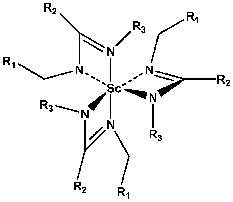
- the precursor is an amidinate type scandium precursor and has the following structural formula:
- the amidinate type scandium precursor herein may be identified as Sc(Amid- Ri, R 2 , R 3 ) 3 .
- the amidinate precursor herein may be identified as Sc(Amid-Et,Me) 3 in that situation where an ethyl group and methyl group serve as the source for the selection of Ri, R 2 and R 3.
- Ri, R 2 and R 3 are preferably selected from alkyls, including methyl, ethyl and/or propyl group functionality.
- the amidinate type scandium precursor herein may therefore have the following structure, which may be abbreviated herein as Sc(Amid-Me) 3 :
- amidinate type scandium precursor herein is preferably prepared according to the following general scheme, where Ri, R 2 and R 3 may be as described above:
- the amidinate type scandium precursors herein provide a very useful combination of dielectric (k) values, thermal stability and processing capability. Attention is directed to FIG. 1 which provides a Thermal Gravimetric Analysis (TGA) and Differential Scanning Calorimetry analysis (DSC) for the amidinate type scandium precursor Sc(Amd-Et,Me) 3 .
- TGA Thermal Gravimetric Analysis
- DSC Differential Scanning Calorimetry analysis
- the amidinate type scandium precursors herein are such that they indicate thermal stability (no breakdown of the structure) in the temperature range of 30 °C to 210 °C, in the absence of any co-reactant.
- the DSC curve in FIG. 1 indicates an endothermic transition centered around 67.2 °C which corresponds to the solid-liquid transition (melting) which occurs prior to the onset of evaporation. Accordingly, in the broad context of the present disclosure, it is contemplated that the amidinate type scandium precursors herein indicates a DSC melting temperature of 67.2 °C, plus or minus 5 °C. The heating rate in the DSC is preferably in the range of 5-10 °C/minute.
- the TGA and DSC evaluation illustrated in FIG. 1 therefore confirms the ability to provide the amidinate type scandium precursors herein in liquid form as well as suitable evaporation characteristics for use in ALD processing.
- FIG. 2 indicates a Thermal Gravimetric Analysis vapor pressure curve under isothermal conditions for the amidinate type scandium precursor Sc(Amid-Me, Et) 3 .
- the precursor indicates a vapor pressure of 0.1 Torr at about 95 °C and a vapor pressure of 1.0 Torr at 130 °C.
- the amidinate type scandium precursors herein indicate a vapor pressure of 0.1 Torr to 1.0 Torr over the temperature range of 95°C to 130 °C.
- Such vapor pressure characteristics are again now suitable for use of the precursors herein for ALD reactors.
- Cp cyclopentadienyl
- Sc(OiPr) 3 ispropoxide
- FIG. 4 indicates a comparative Thermal Gravimetric Analysis of the freshly distilled amidinate type scandium precursor (Sc(Amd-Me,Et) 3 herein compared to a sample of such precursor subjected to prolonged and sustained heating at 150 °C for one week. As can be observed, there is essentially no change in evaporation profiles which therefore confirms the thermal stability of the amidinate type scandium precursors disclosed herein.
- amidinate type scandium precursors herein may be utilized for atomic layer deposition (ALD), which is a thin-film deposition technique based on the precursors herein which may react with a surface followed by removal of unreacted molecules, followed by introduction of a co-reactant, such as water or hydrogen sulfide (H 2 S), which leads to thin film deposition of either Sc 2 0 3 or Sc 2 S 3 .
- ALD atomic layer deposition
- H 2 S hydrogen sulfide
- a substrate temperature in the range of 200 °C to 500 °C can be repeatedly exposed to (a) the amidinate type scandium precursor herein; (b) a chamber purge to remove excess precursor plus any by-products; (c) a co-reactant; and (d) a final chamber purge to remove reaction by products. It is contemplated herein that films containing Sc 2 0 3 or Sc 2 S 3 may therefore now be formed having thicknesses of less than or equal to 300 Angstroms, or in the range of 5 Angstroms to 300 Angstroms.
- the films containing Sc 2 0 3 or Sc 2 S 3 herein when combined with rare earth elements (Y, Gd, La) are further contemplated to produce ternary rare earth scandates of the formula (RESc0 3 or REScS 3 ) where RE stands for rare earth.
- Such ternary scandates are contemplated to have thermal stabilities to 900 °C and dielectric k values of up to 22, which therefore make them suitable as gate insulators for in relatively high speed transistors as well as gate interlayer materials in the integration of new channel materials.
- the films herein containing SC2O3 or SC2S3 formed from the amidinate type scandium precursors herein are such that they can incorporate nitrogen at levels of 0.5 at. % to 10.0 at. %, which can be measured by X-ray photoelectron spectroscopy (XPS).
- a semiconductor process flow may therefore utilize the films disclosed herein for formation of high-k metal gate transistors, for instance.
- a film comprising the ternary scandates herein SC2O3 or SC2S3 may be formed, e.g., using the scandium precursor herein, directly below the gate electrode to provide a gate dialelectric after dummy gate removal to improve channel performance.
- Any number of transistor types and/or formation process flows may benefit from a gate dialectric formed using the films disclosed herein, such as complementary metal-oxide-semiconductor (CMOS) transistor semiconductor devices having N-type or P-type configurations, whether configured with thin or thick gates, and with any number of geometries.
- CMOS complementary metal-oxide-semiconductor
- the resulting gate dialelectric herein may be used in various transistor devices including planar and non-planar configurations, e.g., finned transistor configurations such as tri-gate or FinFET devices, multi- gate devices, nanowire/nanoribbon devices, and so on.
- planar and non-planar configurations e.g., finned transistor configurations such as tri-gate or FinFET devices, multi- gate devices, nanowire/nanoribbon devices, and so on.
- the following examples pertain to further embodiments of the present disclosure and may comprise subject material such as a compound or process for forming a film, wherein the film is suitable for use in semiconductor manufacturing processes.
- the general exemplary procedure is as follows, with the specific compound examples identified below: under a nitrogen atmosphere, 1.0 g (10 mmol) of the amidine in THF (20 mL) was deprotonated with n-BuLi (1.6 M/hexanes, 6.8 mL, 11 mmol) at 78 °C. After the addition was completed, the mixture was warmed to room temperature and stirred for 1 hour. This solution was then added via cannula to a -78 °C flask containing solid ScCl 3 (THF)3 (1.22 g, 3.33 mmol) and the mixture was allowed to slowly warm up overnight. The volatiles were vacuum removed and the residue extracted into hexanes (30 mL) and filtered.
- THF solid ScCl 3
- the yields herein of the subject amidinate type scandium precursors are clearly at a level of at least 50%, more preferably at least 60%, or at least 70%, as well as up to at least 80%. It may therefore be understood that the yields herein of the amidinate type scandium precursor may also be described as falling in the range of 50% to 80%, 60% to 80%, or 70% to 80%.
- Ri, R 2 and R 3 are selected from the group consisting of alkyls, allyls, aryls, heteroaryls, hydrogen, non-metals and metalloids and where Ri, R 2 and R 3 are different or the same.
- This example includes the elements of example 1 wherein Ri, R 2 and R 3 are selected from the group consisting of alkyls selected from methyl, ethyl and/or propyl groups.
- This example includes the elements of example lwherein Ri, R 2 and R 3 are methyl groups.
- Example 4 This example includes the elements of example 1 wherein Ri, R 2 and R 3 are selected from methyl and ethyl groups.
- This example includes the elements of example 1 wherein the compound indicates a vapor pressure of 0.1 Torr to 1.0 Torr over the temperature range 95 °C to 130 °C.
- This example includes the elements of example 1 wherein the compound has a melting point of 67.2 °C, plus or minus 5 °C.
- Ri, R 2 and R 3 are selected from the group consisting of alkyls, allyls, aryls, heteroaryls, hydrogen, non-metals and metalloids and where Ri, R 2 and R 3 are different or the same;
- This example includes the elements of example 7 wherein Ri, R 2 and R 3 are selected from the group consisting of alkyls selected from methyl, ethyl and/or propyl groups.
- This example includes the elements of example 7 wherein Ri, R 2 and R 3 are methyl groups.
- This example includes the elements of example 7 wherein Ri, R 2 and R 3 are selected from methyl and ethyl groups.
- This example includes the elements of example 7 wherein the film has a thickness of 10 Angstroms to 300 Angstroms.
- This example includes the elements of example 7 wherein the compound indicates a vapor pressure of 0.1 Torr to 1.0 Torr over the temperature range 95 °C to 130 °C.
- This example includes the elements of example 7 wherein the compound has a melting point of 67.2 °C, plus or minus 5 °C.
- This example includes the elements of example 7 wherein the co-reactant comprises water.
Abstract
Described are precursor compounds and methods for atomic layer deposition of films containing scandium(III) oxide or scandium(III) sulfide. Such films may be utilized as dielectric layers in semiconductor manufacturing processes, particular for depositing dielectric films and the use of such films in various electronic devices.
Description
SCANDIUM PRECURSOR FOR SC (X OR Sc Sg ATOMIC LAYER
DEPOSITION
TECHNICAL FIELD
The present disclosure relates to scandium precursors for atomic layer deposition of films containing scandium(III) oxide, SC2O3 or scandium (III) sulfide, SC2S3. The scandium precursors, in liquid form and with relatively high thermal stability and relatively high vapor pressure, are conveniently sourced from amidinate-based ligand structures. The films are then employed in semiconductor manufacturing processes, particularly for depositing dielectric films and use of such films in various electronic devices.
BACKGROUND
Atomic layer deposition (ALD) has emerged as a popular technology for the preparation of highly conformal, ultra-thin films. More specifically, ALD has been employed for the deposition of electrically insulating materials with high dielectric constants (high-k dielectrics) as gate insulators in high-speed transistors as well as ultrathin gate interlayers in the integration of new channel materials.
Successful precursors for deposition are preferably volatile, thermally stable and highly reactive. Identifying new and more efficient compounds that satisfy these requirements remains challenging. With regards to high-k dielectric oxides based on SC2O3, many current precursors lack such requirements suitable for ALD processing.
BRIEF DESCRIPTION OF THE DRAWINGS
Features and advantages of various embodiments of the claimed subject matter will become apparent as the following Detailed Description proceeds, and upon reference to the Drawings, wherein like numerals designate like parts, and in which:
FIG. 1 indicates a combined Thermal Gravimetric Analysis (TGA) and Differential Scanning Calorimetry trace of the amidinate type scandium precursor in accordance with the present disclosure;
FIG. 2 indicates a Thermal Gravimetric Analysis vapor pressure curve under isothermal conditions of the amidinate type scandium precursor in accordance with the present disclosure;
FIG. 3 indicates a Thermal Gravimetric Analysis (programmed heating) of the amidinate type scandium precursor herein versus Cp3Sc (Cp = cyclopentadienyl), Sc(THD)3 (THD = 2,2,6,6-tetramethyl-3,4-heptanedionato) and Sc(OiPr)3 (OiPr = isopropoxide).
FIG. 4 indicates a comparative Thermal Gravimetric Analysis of freshly distilled amidinate type scandium precursor herein compared to a sample of such precursor subjected to prolonged and sustained heating at 150 °C for one week.
Although the following Detailed Description will proceed with reference being made to illustrative embodiments, many alternatives, modifications and variations thereof will be apparent to those skilled in the art.
DETAILED DESCRIPTION
The present disclosure is directed to scandium precursors suitable for atomic layer deposition (ALD) of films containing scandium(III) oxide, Sc203 or scandium (III) sulfide, Sc2S3. In an embodiment of the present disclosure the precursor is an amidinate type scandium precursor and has the following structural formula:

wherein Ri, R2 and R3 are selected from the group consisting of alkyls, allyls, aryls, heteroaryls, hydrogen, non-metals and metalloids and where Ri, R2 and R3 are different or the same. Accordingly, in the context of the present disclosure, the amidinate type scandium precursor herein may be identified as Sc(Amid- Ri, R2, R3)3. Alternatively, one may identify the amidinate precursor herein as Sc(Amid-Et,Me)3 in that situation where an ethyl group and methyl group serve as the source for the selection of Ri, R2 and R3.
Accordingly, Ri, R2 and R3 are preferably selected from alkyls, including methyl, ethyl and/or propyl group functionality. In one further preferred embodiment, the amidinate type scandium precursor herein may therefore have the following structure, which may be abbreviated herein as Sc(Amid-Me)3:

The amidinate type scandium precursor herein is preferably prepared according to the following general scheme, where Ri, R2 and R3 may be as described above:

The amidinate type scandium precursors herein provide a very useful combination of dielectric (k) values, thermal stability and processing capability. Attention is directed to FIG. 1 which provides a Thermal Gravimetric Analysis (TGA) and Differential Scanning Calorimetry analysis (DSC) for the amidinate type scandium precursor Sc(Amd-Et,Me)3. As can be seen, the TGA curve shows what may be identified as a clean evaporation profile with near zero residue at a temperature of 210 °C (< 0.1% wt). It may therefore be appreciated that the amidinate type scandium precursors herein are such that they indicate thermal stability (no breakdown of the structure) in the temperature range of 30 °C to 210 °C, in the absence of any co-reactant.
The DSC curve in FIG. 1 indicates an endothermic transition centered around 67.2 °C which corresponds to the solid-liquid transition (melting) which occurs prior to the onset of evaporation. Accordingly, in the broad context of the present disclosure, it is contemplated that the amidinate type scandium precursors herein indicates a DSC melting temperature of 67.2 °C, plus or minus 5 °C. The heating rate in the DSC is preferably in the range of 5-10 °C/minute. The TGA and DSC evaluation illustrated in FIG. 1 therefore confirms the ability to provide the amidinate type scandium precursors herein in liquid form as well as suitable evaporation characteristics for use in ALD processing.
FIG. 2 indicates a Thermal Gravimetric Analysis vapor pressure curve under isothermal conditions for the amidinate type scandium precursor Sc(Amid-Me, Et)3. As can be seen, the precursor indicates a vapor pressure of 0.1 Torr at about 95 °C and a vapor pressure of 1.0 Torr at 130 °C. It is therefore the case that the amidinate type scandium precursors herein indicate a
vapor pressure of 0.1 Torr to 1.0 Torr over the temperature range of 95°C to 130 °C. Such vapor pressure characteristics are again now suitable for use of the precursors herein for ALD reactors.
FIG. 3 next indicates a Thermal Gravimetric Analysis (programmed heating) of the amidinate type scandium precursor herein versus Cp3Sc (Cp = cyclopentadienyl), Sc(THD)3 (THD = 2,2,6,6-tetramethyl-3,4-heptanedionato) and Sc(OiPr)3 (OiPr = ispropoxide). This comparison confirms that the amidinate type scandium precursors herein are relatively more volatile than the other identified scandium precursors, which other precursors also indicated decomposition before volatization appeared to take place, as indicated in part by the erratic behavior at the end of the TGA scan.
FIG. 4 indicates a comparative Thermal Gravimetric Analysis of the freshly distilled amidinate type scandium precursor (Sc(Amd-Me,Et)3 herein compared to a sample of such precursor subjected to prolonged and sustained heating at 150 °C for one week. As can be observed, there is essentially no change in evaporation profiles which therefore confirms the thermal stability of the amidinate type scandium precursors disclosed herein.
As alluded to above, the amidinate type scandium precursors herein may be utilized for atomic layer deposition (ALD), which is a thin-film deposition technique based on the precursors herein which may react with a surface followed by removal of unreacted molecules, followed by introduction of a co-reactant, such as water or hydrogen sulfide (H2S), which leads to thin film deposition of either Sc203 or Sc2S3. Accordingly, during a preferred ALD process a heated substrate (e.g. a substrate temperature in the range of 200 °C to 500 °C) can be repeatedly exposed to (a) the amidinate type scandium precursor herein; (b) a chamber purge to remove excess precursor plus any by-products; (c) a co-reactant; and (d) a final chamber purge to remove reaction by products. It is contemplated herein that films containing Sc203 or Sc2S3 may therefore now be formed having thicknesses of less than or equal to 300 Angstroms, or in the range of 5 Angstroms to 300 Angstroms.
The films containing Sc203 or Sc2S3 herein when combined with rare earth elements (Y, Gd, La) are further contemplated to produce ternary rare earth scandates of the formula (RESc03 or REScS3) where RE stands for rare earth. Such ternary scandates are contemplated to have thermal stabilities to 900 °C and dielectric k values of up to 22, which therefore make them
suitable as gate insulators for in relatively high speed transistors as well as gate interlayer materials in the integration of new channel materials. In addition, the films herein containing SC2O3 or SC2S3 formed from the amidinate type scandium precursors herein are such that they can incorporate nitrogen at levels of 0.5 at. % to 10.0 at. %, which can be measured by X-ray photoelectron spectroscopy (XPS).
A semiconductor process flow may therefore utilize the films disclosed herein for formation of high-k metal gate transistors, for instance. For example, during a gate replacement process a film comprising the ternary scandates herein (SC2O3 or SC2S3) may be formed, e.g., using the scandium precursor herein, directly below the gate electrode to provide a gate dialelectric after dummy gate removal to improve channel performance. Any number of transistor types and/or formation process flows may benefit from a gate dialectric formed using the films disclosed herein, such as complementary metal-oxide-semiconductor (CMOS) transistor semiconductor devices having N-type or P-type configurations, whether configured with thin or thick gates, and with any number of geometries. Moreover, the resulting gate dialelectric herein may be used in various transistor devices including planar and non-planar configurations, e.g., finned transistor configurations such as tri-gate or FinFET devices, multi- gate devices, nanowire/nanoribbon devices, and so on.
The following examples pertain to further embodiments of the present disclosure and may comprise subject material such as a compound or process for forming a film, wherein the film is suitable for use in semiconductor manufacturing processes.
The general exemplary procedure is as follows, with the specific compound examples identified below: under a nitrogen atmosphere, 1.0 g (10 mmol) of the amidine in THF (20 mL) was deprotonated with n-BuLi (1.6 M/hexanes, 6.8 mL, 11 mmol) at 78 °C. After the addition was completed, the mixture was warmed to room temperature and stirred for 1 hour. This solution was then added via cannula to a -78 °C flask containing solid ScCl3(THF)3 (1.22 g, 3.33 mmol) and the mixture was allowed to slowly warm up overnight. The volatiles were vacuum removed and the residue extracted into hexanes (30 mL) and filtered. The colorless residue obtained was bulb-to-bulb distilled at 120-130 °C using a -78° C receiving flask. The final complex was isolated as a white solid (m.p. 64-67 °C determined by DSC) at about 80% yield.
Accordingly, in the broad context of the present disclosure, the yields herein of the subject amidinate type scandium precursors are clearly at a level of at least 50%, more preferably at least 60%, or at least 70%, as well as up to at least 80%. It may therefore be understood that the yields herein of the amidinate type scandium precursor may also be described as falling in the range of 50% to 80%, 60% to 80%, or 70% to 80%.
Example 1
According to this example there is provided a compound having the structural formula:
Example 2
This example includes the elements of example 1 wherein Ri, R2 and R3 are selected from the group consisting of alkyls selected from methyl, ethyl and/or propyl groups.
Example 3
This example includes the elements of example lwherein Ri, R2 and R3 are methyl groups.
Example 4
This example includes the elements of example 1 wherein Ri, R2 and R3 are selected from methyl and ethyl groups.
Example 5
This example includes the elements of example 1 wherein the compound indicates a vapor pressure of 0.1 Torr to 1.0 Torr over the temperature range 95 °C to 130 °C.
Example 6
This example includes the elements of example 1 wherein the compound has a melting point of 67.2 °C, plus or minus 5 °C.
Example 7
According to this example there is provided a process for forming a film comprising
(a) exposing a heated surface to the vapor of the following compound:

(b) exposing the substrate to a co-reactant; and
(c) forming a film on the surface of said substrate wherein said film includes Sc203 or Sc2S3.
Example 8
This example includes the elements of example 7 wherein Ri, R2 and R3 are selected from the group consisting of alkyls selected from methyl, ethyl and/or propyl groups.
Example 9
This example includes the elements of example 7 wherein Ri, R2 and R3 are methyl groups.
Example 10
This example includes the elements of example 7 wherein Ri, R2 and R3 are selected from methyl and ethyl groups.
Example 11
This example includes the elements of example 7 wherein the film has a thickness of 10 Angstroms to 300 Angstroms.
Example 12
This example includes the elements of example 7 wherein the compound indicates a vapor pressure of 0.1 Torr to 1.0 Torr over the temperature range 95 °C to 130 °C.
Example 13
This example includes the elements of example 7 wherein the compound has a melting point of 67.2 °C, plus or minus 5 °C.
Example 14
This example includes the elements of example 7 wherein the co-reactant comprises water.
Example 15
This example includes the elements of example 7 wherein the co-reactant comprises hydrogen sulfide (H2S).
The terms and expressions which have been employed herein are used as terms of description and not of limitation, and there is no intention, in the use of such terms and expressions, of excluding any equivalents of the features shown and described (or portions thereof), and it is recognized that various modifications are possible within the scope of the claims. Accordingly, the claims are intended to cover all such equivalents.
Claims
1. A compound having the structural formula:

2. The compound of claim 1 wherein Ri, R2 and R3 are selected from the group consisting of alkyls selected from methyl, ethyl and/or propyl groups.
3. The compound of claim 1 wherein Ri, R2 and R3 are methyl groups.
4. The compound of claim 1 wherein Ri, R2 and R3 are selected from methyl and ethyl groups.
5. The compound of claim 1 wherein said compound indicates a vapor pressure of 0.1 Torr to 1.0 Torr over the temperature range 95 °C to 130 °C.
The compound of claim 1 or 5 having a melting point of 67.2 °C, plus or minus
7. A process for forming a film comprising
(a) exposing a heated surface to the vapor of the following compound:

(b) exposing the substrate to a co-reactant; and
(c) forming a film on the surface of said substrate wherein said film includes Sc203 or Sc2S3.
8. The process of claim 7 wherein Ri, R2 and R3 are selected from the group consisting of alkyls selected from methyl, ethyl and/or propyl groups.
9. The process of claim 7 wherein Ri, R2 and R3 are methyl groups.
10. The process of claim 7 wherein Ri, R2 and R3 are selected from methyl and ethyl groups.
11. The process of claim 7 wherein said film has a thickness of 5 Angstroms to 300 Angstroms.
12. The process of claim 7 wherein said compound indicates a vapor pressure of 0.1 Torr to 1.0 Torr over the temperature range 95 °C to 130 °C.
13. The process of claim 7 or 12 wherein said compound has a melting point of 67.2 3C, plus or minus 5 °C.
The process of claim 7 wherein said co-reactant comprises water.
The process of claim 7 wherein said co-reactant comprises hydrogen sulfide.
16. The process of claim 7 wherein said film contains nitrogen at levels of 0.5 at. % to 10.0 at. %.
17. The process of claim 7 wherein said film is positioned as a gate dielectric in a transistor.
18. A transistor comprising a gate dielectric containing a film of SC2O3 or SC2S3 wherein said film contains 0.5 at. % to 10.0 at. % nitrogen.
19. The transistor of claim 18 wherein said film has a thickness of 5 Angstroms to 300 Angstroms.
Priority Applications (4)
| Application Number | Priority Date | Filing Date | Title |
|---|---|---|---|
| PCT/US2016/055067 WO2018063410A1 (en) | 2016-10-01 | 2016-10-01 | Scandium precursor for sc2o3 or sc2s3 atomic layer deposition |
| US16/328,536 US11512098B2 (en) | 2016-10-01 | 2016-10-01 | Scandium precursor for SC2O3 or SC2S3 atomic layer deposition |
| US17/962,043 US11866453B2 (en) | 2016-10-01 | 2022-10-07 | Scandium precursor for SC2O3 or SC2S3 atomic layer deposition |
| US18/522,056 US20240092804A1 (en) | 2016-10-01 | 2023-11-28 | Scandium precursor for sc2o3 or sc2s3 atomic layer deposition |
Applications Claiming Priority (1)
| Application Number | Priority Date | Filing Date | Title |
|---|---|---|---|
| PCT/US2016/055067 WO2018063410A1 (en) | 2016-10-01 | 2016-10-01 | Scandium precursor for sc2o3 or sc2s3 atomic layer deposition |
Related Child Applications (2)
| Application Number | Title | Priority Date | Filing Date |
|---|---|---|---|
| US16/328,536 A-371-Of-International US11512098B2 (en) | 2016-10-01 | 2016-10-01 | Scandium precursor for SC2O3 or SC2S3 atomic layer deposition |
| US17/962,043 Continuation US11866453B2 (en) | 2016-10-01 | 2022-10-07 | Scandium precursor for SC2O3 or SC2S3 atomic layer deposition |
Publications (1)
| Publication Number | Publication Date |
|---|---|
| WO2018063410A1 true WO2018063410A1 (en) | 2018-04-05 |
Family
ID=61762887
Family Applications (1)
| Application Number | Title | Priority Date | Filing Date |
|---|---|---|---|
| PCT/US2016/055067 WO2018063410A1 (en) | 2016-10-01 | 2016-10-01 | Scandium precursor for sc2o3 or sc2s3 atomic layer deposition |
Country Status (2)
| Country | Link |
|---|---|
| US (3) | US11512098B2 (en) |
| WO (1) | WO2018063410A1 (en) |
Families Citing this family (2)
| Publication number | Priority date | Publication date | Assignee | Title |
|---|---|---|---|---|
| WO2018063410A1 (en) * | 2016-10-01 | 2018-04-05 | Intel Corporation | Scandium precursor for sc2o3 or sc2s3 atomic layer deposition |
| KR102614467B1 (en) * | 2022-11-30 | 2023-12-14 | 에스케이트리켐 주식회사 | Precursor comprising for scandium or yttrium containg thin film, deposition method of film and semiconductor device of the same |
Citations (2)
| Publication number | Priority date | Publication date | Assignee | Title |
|---|---|---|---|---|
| WO2004046417A2 (en) * | 2002-11-15 | 2004-06-03 | President And Fellows Of Harvard College | Atomic layer deposition using metal amidinates |
| US20060177577A1 (en) * | 2005-02-10 | 2006-08-10 | Thompson David M | Processes for the production of organometallic compounds |
Family Cites Families (2)
| Publication number | Priority date | Publication date | Assignee | Title |
|---|---|---|---|---|
| US20150364772A1 (en) * | 2014-05-30 | 2015-12-17 | GM Global Technology Operations LLC | Method to prepare alloys of platinum-group metals and early transition metals |
| WO2018063410A1 (en) * | 2016-10-01 | 2018-04-05 | Intel Corporation | Scandium precursor for sc2o3 or sc2s3 atomic layer deposition |
-
2016
- 2016-10-01 WO PCT/US2016/055067 patent/WO2018063410A1/en active Application Filing
- 2016-10-01 US US16/328,536 patent/US11512098B2/en active Active
-
2022
- 2022-10-07 US US17/962,043 patent/US11866453B2/en active Active
-
2023
- 2023-11-28 US US18/522,056 patent/US20240092804A1/en active Pending
Patent Citations (2)
| Publication number | Priority date | Publication date | Assignee | Title |
|---|---|---|---|---|
| WO2004046417A2 (en) * | 2002-11-15 | 2004-06-03 | President And Fellows Of Harvard College | Atomic layer deposition using metal amidinates |
| US20060177577A1 (en) * | 2005-02-10 | 2006-08-10 | Thompson David M | Processes for the production of organometallic compounds |
Non-Patent Citations (3)
| Title |
|---|
| DE ROUFFIGNAC, P. ET AL.: "ALD of scandium oxide from scandium tris (N,N' -diisopropylacetamidinate) and water", ELECTROCHEMICAL AND SOLID-STATE LETTERS, vol. 9, no. 6, 2006, pages F45 - F48, XP055501224 * |
| MILANOV, A. P. ET AL.: "Sc203, Er203, and Y203 thin films by MOCVD from volatile guanidinate class of rare-earth precursors", DALTON TRANSACTIONS, vol. 41, no. 45, 2012, pages 13936 - 13947, XP055501225 * |
| MILANOV, A. P. ET AL.: "Synthesis, characterization, and thermal properties of homoleptic rare-earth guanidinates: Promising precursors for MOCVD and ALD of rare-earth oxide thin films", INORGANIC CHEMISTRY, vol. 47, no. 23, 2008, pages 11405 - 11416, XP055501235 * |
Also Published As
| Publication number | Publication date |
|---|---|
| US20230058025A1 (en) | 2023-02-23 |
| US11866453B2 (en) | 2024-01-09 |
| US20240092804A1 (en) | 2024-03-21 |
| US20190202842A1 (en) | 2019-07-04 |
| US11512098B2 (en) | 2022-11-29 |
Similar Documents
| Publication | Publication Date | Title |
|---|---|---|
| US11866453B2 (en) | Scandium precursor for SC2O3 or SC2S3 atomic layer deposition | |
| CN106977540B (en) | Tantalum compound, method for manufacturing integrated circuit device, and integrated circuit device | |
| JP7185394B2 (en) | Tin compound, method for synthesizing same, tin precursor compound for ALD, and method for forming tin-containing material film | |
| JP2016540038A (en) | Metal complexes containing amidoimine ligands | |
| KR102638657B1 (en) | Metal complexes containing cyclopentadienyl ligands | |
| US20180258526A1 (en) | Chemical vapor deposition raw material including organoruthenium compound and chemical deposition method using the chemical vapor deposition raw material | |
| KR20180007815A (en) | Aluminum compound and methods of forming thin film and integrated circuit device | |
| US20170117142A1 (en) | Organic Germanium Amine Compound and Method for Depositing Thin Film Using the Same | |
| KR20190040354A (en) | Metal complexes containing allyl ligands | |
| KR102033540B1 (en) | Metal triamine compound, its preparation method and composition for depositing a metal-containing thin film comprising the same | |
| KR101643480B1 (en) | Chemical vapor deposition raw material comprising organoplatinum compound, and chemical vapor deposition method using the chemical vapor deposition raw material | |
| US20180282866A1 (en) | Ruthenium precursor, preparation method therefor and method for forming thin film using same | |
| KR20120131114A (en) | Compound and precursor composition For deposition of silicon compound | |
| US7722926B2 (en) | Organometallic compounds and methods of forming thin films including the use of the same | |
| JP6624997B2 (en) | Trinuclear hafnium oxo-alkoxo complex and method for producing the same | |
| Triyoso et al. | Atomic layer deposited TaCy metal gates: Impact on microstructure, electrical properties, and work function on HfO2 high-k dielectrics | |
| JP5088232B2 (en) | Method for producing hafnium complex | |
| Lee et al. | Group IV transition metal (M= Zr, Hf) precursors for high-κ metal oxide thin films | |
| KR20200067508A (en) | Group iv transition metal compounds, preparation method thereof and process for the formation of thin films using the same | |
| KR101770152B1 (en) | composition comprising boron-containing compound, boron-containing thin film and method for manufacturing boron-containing thin film | |
| KR102129055B1 (en) | Zirconium aminoalkoxide precursors, preparation method thereof and process for thin film formation using the same | |
| TWI630210B (en) | Precursors for the production of thin oxide layers and the use thereof | |
| KR102569201B1 (en) | Method of synthesizing organometallic compound and method for the formation of thin films using thereof | |
| KR101319503B1 (en) | Hafnium amide complex manufacturing method and hafnium-containing oxide film | |
| KR100590051B1 (en) | Precursors of lanthanide oxide and preparing method thereof |
Legal Events
| Date | Code | Title | Description |
|---|---|---|---|
| 121 | Ep: the epo has been informed by wipo that ep was designated in this application |
Ref document number: 16918099 Country of ref document: EP Kind code of ref document: A1 |
|
| NENP | Non-entry into the national phase |
Ref country code: DE |
|
| 122 | Ep: pct application non-entry in european phase |
Ref document number: 16918099 Country of ref document: EP Kind code of ref document: A1 |