WO2018043894A1 - 금속-go 코어-쉘 복합 나노구조체, 이를 포함하는 비휘발성 저항 변화 메모리 소자, 및 상기 메모리 소자의 제조 방법 - Google Patents
금속-go 코어-쉘 복합 나노구조체, 이를 포함하는 비휘발성 저항 변화 메모리 소자, 및 상기 메모리 소자의 제조 방법 Download PDFInfo
- Publication number
- WO2018043894A1 WO2018043894A1 PCT/KR2017/006697 KR2017006697W WO2018043894A1 WO 2018043894 A1 WO2018043894 A1 WO 2018043894A1 KR 2017006697 W KR2017006697 W KR 2017006697W WO 2018043894 A1 WO2018043894 A1 WO 2018043894A1
- Authority
- WO
- WIPO (PCT)
- Prior art keywords
- metal
- core
- memory device
- shell
- change memory
- Prior art date
- Legal status (The legal status is an assumption and is not a legal conclusion. Google has not performed a legal analysis and makes no representation as to the accuracy of the status listed.)
- Ceased
Links
Images





Classifications
-
- H—ELECTRICITY
- H10—SEMICONDUCTOR DEVICES; ELECTRIC SOLID-STATE DEVICES NOT OTHERWISE PROVIDED FOR
- H10N—ELECTRIC SOLID-STATE DEVICES NOT OTHERWISE PROVIDED FOR
- H10N70/00—Solid-state devices having no potential barriers, and specially adapted for rectifying, amplifying, oscillating or switching
- H10N70/801—Constructional details of multistable switching devices
- H10N70/881—Switching materials
-
- H—ELECTRICITY
- H10—SEMICONDUCTOR DEVICES; ELECTRIC SOLID-STATE DEVICES NOT OTHERWISE PROVIDED FOR
- H10N—ELECTRIC SOLID-STATE DEVICES NOT OTHERWISE PROVIDED FOR
- H10N70/00—Solid-state devices having no potential barriers, and specially adapted for rectifying, amplifying, oscillating or switching
-
- H—ELECTRICITY
- H10—SEMICONDUCTOR DEVICES; ELECTRIC SOLID-STATE DEVICES NOT OTHERWISE PROVIDED FOR
- H10N—ELECTRIC SOLID-STATE DEVICES NOT OTHERWISE PROVIDED FOR
- H10N70/00—Solid-state devices having no potential barriers, and specially adapted for rectifying, amplifying, oscillating or switching
- H10N70/011—Manufacture or treatment of multistable switching devices
- H10N70/021—Formation of switching materials, e.g. deposition of layers
-
- H—ELECTRICITY
- H10—SEMICONDUCTOR DEVICES; ELECTRIC SOLID-STATE DEVICES NOT OTHERWISE PROVIDED FOR
- H10N—ELECTRIC SOLID-STATE DEVICES NOT OTHERWISE PROVIDED FOR
- H10N70/00—Solid-state devices having no potential barriers, and specially adapted for rectifying, amplifying, oscillating or switching
- H10N70/801—Constructional details of multistable switching devices
-
- H—ELECTRICITY
- H10—SEMICONDUCTOR DEVICES; ELECTRIC SOLID-STATE DEVICES NOT OTHERWISE PROVIDED FOR
- H10N—ELECTRIC SOLID-STATE DEVICES NOT OTHERWISE PROVIDED FOR
- H10N70/00—Solid-state devices having no potential barriers, and specially adapted for rectifying, amplifying, oscillating or switching
- H10N70/801—Constructional details of multistable switching devices
- H10N70/881—Switching materials
- H10N70/883—Oxides or nitrides
Definitions
- the present invention relates to a metal-GO core-shell composite nanostructure, a nonvolatile resistance change memory (ReRAM) device including the metal-GO core-shell composite nanostructure, and a method of manufacturing the memory device.
- ReRAM resistance change memory
- ReRAM resistive random-access memory
- Hybrid systems formed primarily as inorganic nanoparticles (NPs) incorporated into organic matrices have been proposed as one type of ReRAM.
- AuNP @ GO gold nanoparticles wrapped by graphene oxide (GO) for device fabrication are compatible. It is easy to control, and environmentally friendly.
- the present application describes data for gold nanospheres (AuNS @ GO) based nonvolatile memory devices wrapped with graphene oxide with bistable properties.
- AuNS @ GO based on a single step, solution process as the dielectric layer of the ReRAM device.
- TEM and SEM analyzes were measured to confirm the morphology and thickness of GO layers coated on different AuNS.
- Current-voltage (I-V) and switching measurements were performed to investigate the bistable memory performance in the device.
- the retention characteristics of the multilevel current state in the device cell were measured to investigate the stability of each cell.
- the dual stability resistive switching memory mechanism of Au / AuNS @ GO / Al / PES devices can be described using charge capture in different AuNPs.
- Korean Patent Application Publication No. 2016-0048444 discloses an organic field effect transistor based nonvolatile memory device including an organic semiconductor layer and a gate insulating layer, and a polymer charge storage layer between the organic semiconductor layer and the gate insulating layer. And a non-volatile organic memory device further comprising a double layer of nanoparticle floating gate layer.
- the present application provides a metal-GO core-shell composite nanostructure, a nonvolatile resistance change memory device including the metal-GO core-shell composite nanostructure, and a method of manufacturing the memory device.
- a metal-GO core-shell composite nano comprising a metal core and a shell of a plurality of graphene oxide (GO) sheets wrapping the core.
- GO graphene oxide
- the lower electrode formed on the substrate;
- a metal-GO core-shell composite nanostructure layer comprising a metal core formed on the lower electrode and a dielectric shell of a plurality of graphene oxide sheets wrapping the core;
- an upper electrode formed on the composite nanostructure layer.
- a third aspect of the present disclosure includes forming a lower electrode on a substrate; Forming a metal-GO core-shell composite nanostructure layer including a metal core and a dielectric shell of a plurality of graphene oxide sheets wrapping the core on the lower electrode; And forming an upper electrode on the composite nanostructure layer, wherein forming the composite nanostructure layer is performed by a single step, solution process. to provide.
- the metal-GO core-shell composite nanostructure can simultaneously serve as a charge trap and a dielectric layer in a nonvolatile resistance change memory device, thereby reducing the ratio of simple structures.
- a volatile resistance change memory device can be obtained.
- the step of forming a composite nanostructure layer including the metal-GO core-shell composite nanostructure is a single step, a solution process to reduce the manufacturing time and manufacturing A reduction in the unit cost can be achieved.
- a nonvolatile resistive change memory device comprising a metal-GO core-shell composite nanostructure has excellent dual stability electrical switching behavior, a higher ON / OFF ratio than 2 orders, -2.5 V It has a low operating voltage and is environmentally friendly because it is manufactured based on a solution process.
- Figure 1a in one embodiment of the present application, a schematic diagram showing the manufacturing process of the metal-GO core-shell composite nanostructure.
- FIG. 1B is a schematic diagram illustrating a nonvolatile resistance change memory device in an embodiment of the present disclosure.
- 1C is a cross-sectional view illustrating a nonvolatile resistance change memory device according to an exemplary embodiment of the present disclosure.
- FIG. 2 is a schematic diagram illustrating a manufacturing process of a nonvolatile resistance change memory device according to an exemplary embodiment of the present disclosure.
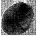
- 3A is a TEM image of AuNS @ GO with a GO shell of 5 nm thickness in one embodiment of the present application.
- FIG. 3B is an SEM image showing drop casting of AuNS @ GO on a substrate in one embodiment of the present application.
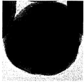
- 4A-4C are TEM images of each AuNS @ GO with GO shell thicknesses of 2 nm, 5 nm, and 7 nm, respectively, in one embodiment of the present application.
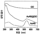
- FIG. 5A is UV-Vis absorption spectra of GO, AuNS, and AuNS @ GO in one embodiment of the present application.
- 5B shows Raman spectra of GO, AuNS, and AuNS @ GO in one embodiment of the present application.
- FIG. 6A is a graph illustrating I-V switching characteristics of an Au / AuNS @ GO / Al device coated with a 5 nm thick GO layer in an embodiment of the present disclosure.
- FIG. 6B is a graph showing log-log I-V switching characteristics of an Au / AuNS @ GO / Al device coated with a 5 nm thick GO layer in one embodiment of the present disclosure.
- 6C is a graph illustrating an endurance cycle of an Au / AuNS @ GO / Al device in one embodiment of the present application.
- FIG. 6D is a graph showing the retention time of Au / AuNS @ GO / Al devices at a read voltage of 0.5 V in one embodiment of the present application.
- 7A and 7B are graphs illustrating I-V switching characteristics of Au / AuNS @ GO / Al devices coated with GO layers having a thickness of 7 nm and 2 nm, respectively, in one embodiment of the present application.
- FIG. 8A is a graph showing the sustain cycle of an Au / AuNS @ GO / Al device with a GO shell of 7 nm thickness in one embodiment of the present application.
- 8B is a graph showing the storage time at 0.5 V read voltage of an Au / AuNS @ GO / Al device with a GO shell of 7 nm thickness in one embodiment of the present application.
- FIG. 9A is a linear fitting graph of I-V curves at log-log scale showing ohmic and SCLC mechanisms in one embodiment of the present disclosure.
- 9B is a Poole-Frenkel emission fitting graph, in one embodiment of the present disclosure.
- 9C is a Schottky release fitting graph, in one embodiment of the present disclosure.
- FIG. 10A is a schematic diagram illustrating a mechanism of a trapped charge limited current (TCLC) and a space charged limited current (SCLC) in an ON state of a memory device according to an embodiment of the present disclosure. to be.
- TCLC trapped charge limited current
- SCLC space charged limited current
- 10B is a schematic diagram showing an OFF state of a memory element in one embodiment of the present application.
- the term “combination of these” included in the expression of the makushi form means one or more mixtures or combinations selected from the group consisting of the constituents described in the expression of the makushi form, wherein the constituents It means to include one or more selected from the group consisting of.
- a metal-GO core-shell composite nano comprising a metal core and a shell of a plurality of graphene oxide (GO) sheets wrapping the core.
- GO graphene oxide
- the metal-GO core-shell composite nanostructures can be confirmed that the structure of the plurality of graphene oxide sheets irregularly wrap the metal core.
- the metal may be any metal that can serve as a charge trap, for example, conductive metals such as gold (Au), silver (Ag), copper (Cu), aluminum ( Al), tantalum (Ta), tungsten (W), ruthenium (Ru), molybdenum (Mo), nickel (Ni), niobium (Nb), vanadium (V), titanium (Ti), and their It may be to include a metal selected from the group consisting of combinations, but is not limited thereto.
- conductive metals such as gold (Au), silver (Ag), copper (Cu), aluminum ( Al), tantalum (Ta), tungsten (W), ruthenium (Ru), molybdenum (Mo), nickel (Ni), niobium (Nb), vanadium (V), titanium (Ti), and their It may be to include a metal selected from the group consisting of combinations, but is not limited thereto.
- the lapping may be due to the electrostatic interaction between the metal core and the graphene oxide sheets.
- the lapping charges a positive charge by decorating a functional group such as an amine group on the surface of the graphene oxide having a negative charge, and then capping the material having an anionic functional group to cap the negatively charged metal.
- Dispersed in the charged graphene oxide solution may be performed by using an electrostatic interaction.
- the metal core may have a size of about 20 nm to about 200 nm.
- the size of the metal core may vary depending on the shape of the metal core, and may mean a diameter in the form of a sphere, and may be a diameter of a long axis or a diameter of a short axis in the case of an ellipse.
- the size of the metal core is, for example, about 20 nm to about 200 nm, about 30 nm to about 200 nm, about 40 nm to about 200 nm, about 50 nm to about 200 nm, about 60 nm to about 200 nm , About 70 nm to about 200 nm, about 80 nm to about 200 nm, about 90 nm to about 200 nm, about 100 nm to about 200 nm, about 130 nm to about 200 nm, about 150 nm to about 200 nm, about 180 nm to about 200 nm, about 20 nm to about 180 nm, about 20 nm to about 150 nm, about 20 nm to about 130 nm, about 20 nm to about 100 nm, about 20 nm to about 90 nm, about 20 nm To about 80 nm, about 20 nm to about 70 nm, about 20 nm to about 60 nm, about 20
- the thickness of the shell formed by the GO sheets may be about 2 nm or more.
- the thickness of the shell is about 2 nm to about 100 nm, about 4 nm to about 100 nm, about 6 nm to about 100 nm, about 8 nm to about 100 nm, about 10 nm to about 100 nm, about 20 nm to about 100 nm, about 30 nm to about 100 nm, about 40 nm to about 100 nm, about 50 nm to about 100 nm, about 60 nm to about 100 nm, about 70 nm to about 100 nm, about 80 nm To about 100 nm, about 90 nm to about 100 nm, about 2 nm to about 90 nm, about 2 nm to about 80 nm, about 2 nm to about 70 nm, about 2 nm to about 60 nm, about 2 nm to about 50 nm, about
- the thickness of the shell When the thickness of the shell is thinner than 2 nm, it cannot exhibit any hysteresis behavior indicating the optimum thickness required for the graphene oxide to cover the metal core, and the metal-GO core-shell composite nanostructure is described herein.
- the shell When introduced into the nonvolatile resistance change memory element according to the second and third sides, it may not have sufficient coating for current to pass from the lower electrode to the upper electrode.
- the shell is thicker than 100 nm, it is necessary to apply a relatively high voltage to operate the memory device, but is not limited to a specific range.
- the diameter of the metal core is sufficiently larger than the thickness of the GO shell, but the ratio is not particularly limited.
- the ratio of the size of the metal core to the thickness of the shell formed by the GO sheets is about 1 to 100: 1, about 10 to 100: 1, about 20 to 100: 1, about 30 to 100: 1 , About 40 to 100: 1, about 50 to 100: 1, about 60 to 100: 1, about 70 to 100: 1, about 80 to 100: 1, about 90 to 100: 1, about 1 to 90: 1, about 1 to 90: 1, about 1 to 80: 1, about 1 to 70: 1, about 1 to 60: 1, about 1 to 50: 1, about 1 to 40: 1, about 1 to 30: 1, about 1 to 20: 1, about 1 to 10: 1, about 5 to 50: 1, about 10 to 50: 1, about 5 to 40: 1, about 10 to 40: 1, or about 10 to 30: 1.
- a second aspect of the present application the lower electrode formed on the substrate; A metal-GO core-shell composite nanostructure layer comprising a metal core formed on the lower electrode and a dielectric shell of a plurality of graphene oxide sheets wrapping the core; And an upper electrode formed on the composite nanostructure layer.
- FIGS. 1B and 1C illustrate the structure of the nonvolatile resistance change memory device 101.
- a plurality of lower electrode 120 lines are stacked on the substrate 110, and the substrate 110 and the plurality of substrates are stacked on the substrate 110.
- the composite nanostructure layer 130 is stacked on the lower electrode 120 line.
- the composite nanostructure layer 130 may be deposited by drop casting, and the composite nanostructure layer 130 may include a plurality of metal-GO core-shell composite nanostructures according to the first aspect of the present disclosure. 140.
- the plurality of metal-GO core-shell composite nanostructures 140 may be irregularly positioned within the composite nanostructure layer 130.
- the plurality of upper electrode 150 lines may be stacked on the composite nanostructure layer 130 in a vertical direction to the plurality of lower electrode 120 lines to have a cross bar structure.
- the metal forming the core may be any metal that can serve as a charge trap, for example, conductive metals (Au), silver (Ag), copper (Cu ), Aluminum (Al), tantalum (Ta), tungsten (W), ruthenium (Ru), molybdenum (Mo), nickel (Ni), niobium (Nb), vanadium (V), titanium (Ti) And, and may be to include a metal selected from the group consisting of, but is not limited thereto.
- the metal forming the core may act as a charge trap center in the nonvolatile resistance change memory device
- the graphene oxide sheet forming the shell is the nonvolatile It can act as a dielectric in a resistive change memory device.
- the metal-GO core-shell composite nanostructure may simultaneously serve as a charge trap and a dielectric layer in the nonvolatile resistance change memory device.
- the lapping may be due to the electrostatic interaction between the metal core and the graphene oxide sheets.
- the lapping charges a positive charge by decorating a functional group such as an amine group on the surface of the graphene oxide having a negative charge, and then capping the material having an anionic functional group to charge the metal having the negative charge with the positive charge.
- Dispersion in the graphene oxide solution may be performed using an electrostatic interaction.
- the metal core may have a size of about 20 nm to about 200 nm.
- the size of the metal core may vary depending on the shape of the metal core.
- the diameter of the metal core may mean a diameter in the form of a sphere, and may be a diameter of a long axis or a diameter of a short axis in the case of an elliptical shape.
- the size of the metal core is, for example, about 20 nm to about 200 nm, about 30 nm to about 200 nm, about 40 nm to about 200 nm, about 50 nm to about 200 nm, about 60 nm to about 200 nm , About 70 nm to about 200 nm, about 80 nm to about 200 nm, about 90 nm to about 200 nm, about 100 nm to about 200 nm, about 130 nm to about 200 nm, about 150 nm to about 200 nm, about 180 nm to about 200 nm, about 20 nm to about 180 nm, about 20 nm to about 150 nm, about 20 nm to about 130 nm, about 20 nm to about 100 nm, about 20 nm to about 90 nm, about 20 nm To about 80 nm, about 20 nm to about 70 nm, about 20 nm to about 60 nm, about 20
- the size of the metal core may be an independent element in terms of ON / OFF ratio and bias switching voltage, which are characteristics of the nonvolatile resistance change memory device, but is not limited thereto.
- the thickness of the shell formed by the GO sheets may be about 2 nm or more.
- the thickness of the shell is about 2 nm to about 100 nm, about 4 nm to about 100 nm, about 6 nm to about 100 nm, about 8 nm to about 100 nm, about 10 nm to about 100 nm, about 20 nm to about 100 nm, about 30 nm to about 100 nm, about 40 nm to about 100 nm, about 50 nm to about 100 nm, about 60 nm to about 100 nm, about 70 nm to about 100 nm, about 80 nm To about 100 nm, about 90 nm to about 100 nm, about 2 nm to about 90 nm, about 2 nm to about 80 nm, about 2 nm to about 70 nm, about 2 nm to about 60 nm, about 2 nm to about 50 nm, about
- the metal-GO core-shell composite nanostructure When the thickness of the shell is thinner than 2 nm, no hysteresis behavior exhibits the optimum thickness needed for the graphene oxide to cover the metal core, and the metal-GO core-shell composite nanostructure is referred to as the non-volatile. It may not have sufficient coating for current to pass from the bottom electrode to the top electrode when introduced into the resistive change memory element. On the other hand, if the shell is thicker than 100 nm, it is necessary to apply a relatively high voltage to operate the memory device, but is not limited to a specific range.
- the diameter of the metal core is sufficiently larger than the thickness of the GO shell, but the ratio is not particularly limited.
- the ratio of the size of the metal core to the thickness of the shell formed by the GO sheets is about 1 to 100: 1, about 10 to 100: 1, about 20 to 100: 1, about 30 to 100: 1 , About 40 to 100: 1, about 50 to 100: 1, about 60 to 100: 1, about 70 to 100: 1, about 80 to 100: 1, about 90 to 100: 1, about 1 to 90: 1, about 1 to 90: 1, about 1 to 80: 1, about 1 to 70: 1, about 1 to 60: 1, about 1 to 50: 1, about 1 to 40: 1, about 1 to 30: 1, about 1 to 20: 1, about 1 to 10: 1, about 5 to 50: 1, about 10 to 50: 1, about 5 to 40: 1, about 10 to 40: 1, or about 10 to 30: 1.
- the substrate may be glass, polymer, silicone, or a transparent conductive material
- the polymer may be poly (ether sulfide), PES or poly (ethylene terephthalate)
- Poly (ethylene terephthalate) may be included, but is not limited thereto.
- the lower electrode may be unnecessary, but is not limited thereto.
- the lower electrode is aluminum (Al), gold (Au), platinum (Pt), silver (Ag), nickel (Ni), copper (Cu), cobalt (Co), iron (Fe) ), And combinations thereof, but is not limited thereto.
- the upper electrode is gold (Au), platinum (Pt), silver (Ag), nickel (Ni), copper (Cu), cobalt (Co), iron (Fe), aluminum (Al) ), And combinations thereof, but is not limited thereto.
- the nonvolatile resistance change memory device may have a cross bar structure.
- the crossbar structure refers to a structure in which a plurality of upper electrode lines positioned on an upper side and a plurality of lower electrode lines positioned on a lower side thereof are arranged to cross each other.
- Such a crossbar array structure includes arranging nonvolatile resistance change memory devices in a crossbar array structure and selectively activating electrode lines respectively connected to the plurality of nonvolatile resistance change memory devices to store data in a desired nonvolatile resistance change memory device. Read the stored data.
- a third aspect of the present disclosure includes forming a lower electrode on a substrate; Forming a metal-GO core-shell composite nanostructure layer including a metal core and a dielectric shell of a plurality of graphene oxide sheets wrapping the core on the lower electrode; And forming an upper electrode on the composite nanostructure layer, wherein forming the composite nanostructure layer is performed by a single step, solution process. to provide.
- Figure 2 is a schematic diagram showing a manufacturing method of the nonvolatile resistance change memory device, with reference to Figure 2 of the third aspect of the present application in the order of the manufacturing method of the nonvolatile resistance change memory device An implementation example will be described.
- the substrate may be, for example, glass, polymer, silicone, or a transparent conductive material, the polymer being poly (ether sulfide), PES or poly (ethylene terephthalate) [poly (ethylene terephthalate), but is not limited thereto.
- the substrate is a transparent conductive material
- the lower electrode may be unnecessary, but is not limited thereto.
- the lower electrode is aluminum (Al), gold (Au), platinum (Pt), silver (Ag), nickel (Ni), copper (Cu), cobalt (Co), iron (Fe) ), And combinations thereof, but is not limited thereto.
- the process for forming the lower electrode on the substrate includes physical vapor deposition (PVD), chemical vapor deposition (CVD), sputtering (sputtering), pulse Pulsed laser deposition (PLD), thermal evaporation, electron beam evaporation, atomic layer deposition (ALD), molecular beam epitaxy (MBE), solutions It may include, but is not limited to, a process selected from the group consisting of a process, and combinations thereof.
- a composite nanostructure layer comprising a plurality of metal-GO core-shell composite nanostructures, according to the first aspect of the present disclosure, is laminated on the substrate and the lower electrode.
- the stack of composite nanostructure layers may be vacuum filtration, spin-coating, spray-coating, ink-jet printing, drop-casting, or standard. It may be by lithography (standard lithography), but is not limited thereto.
- the metal forming the core may be any metal that can serve as a charge trap, for example, conductive metals (Au), silver (Ag), copper (Cu ), Aluminum (Al), tantalum (Ta), tungsten (W), ruthenium (Ru), molybdenum (Mo), nickel (Ni), niobium (Nb), vanadium (V), titanium (Ti) And, and may be to include a metal selected from the group consisting of, but is not limited thereto.
- the metal forming the core may act as a charge trap center in the nonvolatile resistance change memory device
- the graphene oxide sheet is the nonvolatile resistance change memory device It can act as a dielectric within. Accordingly, the metal-GO core-shell composite nanostructure may simultaneously serve as a charge trap and a dielectric layer in the nonvolatile resistance change memory device.
- the lapping may be due to the electrostatic interaction between the metal core and the graphene oxide sheets.
- the lapping charges a positive charge by decorating a functional group such as an amine group on the surface of the graphene oxide having a negative charge, and then capping the material having an anionic functional group to charge the metal having the negative charge with the positive charge.
- Dispersion in the graphene oxide solution may be performed using an electrostatic interaction, but is not limited thereto.
- the metal core may have a size of about 20 nm to about 200 nm.
- the size of the metal core may vary depending on, for example, the shape of the metal core.
- the metal core may have a diameter in the form of a sphere, and the diameter of the metal core may be a diameter of a long axis or a short axis.
- the size of the metal core is, for example, about 20 nm to about 200 nm, about 30 nm to about 200 nm, about 40 nm to about 200 nm, about 50 nm to about 200 nm, about 60 nm to about 200 nm , About 70 nm to about 200 nm, about 80 nm to about 200 nm, about 90 nm to about 200 nm, about 100 nm to about 200 nm, about 130 nm to about 200 nm, about 150 nm to about 200 nm, about 180 nm to about 200 nm, about 20 nm to about 180 nm, about 20 nm to about 150 nm, about 20 nm to about 130 nm, about 20 nm to about 100 nm, about 20 nm to about 90 nm, about 20 nm To about 80 nm, about 20 nm to about 70 nm, about 20 nm to about 60 nm, about 20
- the diameter of the metal core may be an independent element in terms of ON / OFF ratio and bias switching voltage, which are characteristics of the nonvolatile resistance change memory device, but is not limited thereto.
- the thickness of the shell formed by the GO sheets may be about 2 nm or more.
- the thickness of the shell is about 2 nm to about 100 nm, about 4 nm to about 100 nm, about 6 nm to about 100 nm, about 8 nm to about 100 nm, about 10 nm to about 100 nm, about 20 nm to about 100 nm, about 30 nm to about 100 nm, about 40 nm to about 100 nm, about 50 nm to about 100 nm, about 60 nm to about 100 nm, about 70 nm to about 100 nm, about 80 nm To about 100 nm, about 90 nm to about 100 nm, about 2 nm to about 90 nm, about 2 nm to about 80 nm, about 2 nm to about 70 nm, about 2 nm to about 60 nm, about 2 nm to about 50 nm, about
- the metal-GO core-shell composite nanostructure When the thickness of the shell is thinner than 2 nm, no hysteresis behavior exhibits the optimum thickness needed for the graphene oxide to cover the metal core, and the metal-GO core-shell composite nanostructure is referred to as the non-volatile. It may not have sufficient coating for current to pass from the bottom electrode to the top electrode when introduced into the resistive change memory element. On the other hand, if the shell is thicker than 100 nm, it is necessary to apply a relatively high voltage to operate the memory device, but is not limited to a specific range.
- the diameter of the metal core is sufficiently larger than the thickness of the GO shell, but the ratio is not particularly limited.
- the ratio of the size of the metal core to the thickness of the shell formed by the GO sheets is about 1 to 100: 1, about 10 to 100: 1, about 20 to 100: 1, about 30 to 100: 1 , About 40 to 100: 1, about 50 to 100: 1, about 60 to 100: 1, about 70 to 100: 1, about 80 to 100: 1, about 90 to 100: 1, about 1 to 90: 1, about 1 to 90: 1, about 1 to 80: 1, about 1 to 70: 1, about 1 to 60: 1, about 1 to 50: 1, about 1 to 40: 1, about 1 to 30: 1, about 1 to 20: 1, about 1 to 10: 1, about 5 to 50: 1, about 10 to 50: 1, about 5 to 40: 1, about 10 to 40: 1, or about 10 to 30: 1.
- the upper electrode is stacked on the composite nanostructure layer, the upper electrode is gold (Au), platinum (Pt), silver (Ag), nickel (Ni), copper (Cu), It may include, but is not limited to, a material selected from the group consisting of cobalt (Co), iron (Fe), aluminum (Al), and combinations thereof.
- the process for forming the upper electrode on the composite nanostructure layer includes physical vapor deposition (PVD), chemical vapor deposition (CVD), sputtering (sputtering) ), Pulsed laser deposition (PLD), thermal evaporation, electron beam evaporation, atomic layer deposition (ALD), molecular beam epitaxy (MBE) ), A solution process, and a combination thereof may be included, but is not limited thereto.
- the nonvolatile resistance change memory device may have a cross bar structure.
- the crossbar structure refers to a structure in which a plurality of upper electrode lines positioned on an upper side and a plurality of lower electrode lines positioned on a lower side thereof are arranged to cross each other.
- Such a crossbar array structure includes arranging nonvolatile resistance change memory devices in a crossbar array structure and selectively activating electrode lines respectively connected to the plurality of nonvolatile resistance change memory devices to store data in a desired nonvolatile resistance change memory device. Read the stored data.
- AuNS with a diameter of 55 nm that is citrate-capped by citrate is known method [Li, JF; Tian, XD; Li, SB; Anema, JR; Yang, ZL; Ding, Y .; Wu, YF; Zeng, YM; Chen, QZ; Ren, B .; Wang, ZL; Tian, ZQ Surface Analysis Using Shell-Isolated Nanoparticle-Enhanced Raman Spectroscopy. Nat. Protocols 2013, 8 , 52-65.
- 200 mL of 0.01 wt% aqueous solution of chloroauric acid was added to a round bottom flask and heated to 130 ° C. Thereafter, 1.4 mL of 1 wt% sodium citrate was quickly added to the heated solution and stirred for 30 minutes. Finally, a dark pink AuNS solution was obtained.
- Graphene oxide was first prepared using a modified Hummer method.
- known methods [Hong, J .; Char, K .; Kim, B.-S. Hollow Capsules of Reduced Graphene Oxide Nanosheets Assembled on a Sacrificial Colloidal Particle. The Journal of Physical Chemistry Letters 2010, 1 , 3442-3445, generated positive charges by decorating amine groups on the GO surface.
- a 50 mL GO solution prepared with a negative charge is N-ethyl-N '-(3-dimethyl aminopropyl) carbodiimide methoxide (N-ethyl-N'-(3-dimethyl aminopropyl) carbodiimide methiodide, EDC] 500 mg, 5 mL of ethylenediamine, and 1 mL of triethyl amine were stirred for 4 hours.
- the prepared AuNS was centrifuged and the resulting precipitate was dispersed in the same volume of the positively charged GO solution and stirred gently overnight. The solution produced by this procedure was washed by centrifugation to remove residual reactants and to obtain AuNS @ GO (FIG. 1A).
- Au upper electrode lines with a width of 100 mm and a thickness of 50 nm were thermally deposited at a deposition rate of 0.1 nm / s at 106 mbar pressure.
- the upper electrode lines were arranged perpendicular to the Al lower electrode lines, yielding an array of memory cells having an active area of 100 x 100 mm (FIGS. 1B and 1C).
- a Raman assay was obtained using HORIABA Jobin Yvon at the excitation wavelength.
- the surface shape is an atomic force microscope using a Dimension 3100 scanning force microscope (Digital Instrument) and a field emission scanning electron microscopy (FE-SEM) (JSM-6700F, JEOL) in the tapping mode. atomic force microscopy (AFM).
- the electrical properties of the fabricated device were measured under ambient conditions using semiconductor systems (E5270B, HP4284A, and Agilent Technologies).
- Gold nanospheres (AuNS @ GO) wrapped with graphene oxide were prepared based on electrostatic interactions between AuNS and GO sheets. Based on the electrostatic interaction, AuNS capped by citrate was wrapped by GO. As shown in the TEM image (FIG. 3A), AuNPs were elliptical and the diameter of the long-axis was 50 nm to 60 nm. In addition, the rough crinkled features associated with flexible, ultrathin graphene sheets were clearly observed on the AuNS surface, which exhibited a GO shell thickness of about 5 nm. In addition, different GO shells with thicknesses of 2 nm to 7 nm were also prepared (FIG. 4).
- first order scattering in the E 2g mode of graphene sp 2 carbon atoms raised the peak at ⁇ 1580 cm ⁇ 1 , which was designated as G-band.
- the D-band and G-band were observed at ⁇ 1337 cm ⁇ 1 and ⁇ 1595 cm ⁇ 1 , respectively.
- two characteristic peaks were still observed, and the positions of the D- and G-bands remained the same.
- AuNS Gold nanospheres
- FIG. 1A Gold nanospheres
- FIG. 1B Gold nanospheres
- the AuNS @ GO layer was drop cast on an Al coated PES substrate (FIG. 3B).
- Au strips as the top electrode were deposited using an evaporator.
- 6A shows typical current-voltage (I-V) characteristics, in which characteristic hysteresis can be observed in the I-V curve corresponding to a device manufactured from AuNS @ GO. Starting from the low-conductivity OFF state in the fabricated device, the current gradually increased as the positive voltage applied increased (FIG. 6B).
- the current remained low until a turn-on voltage of about -2.5 V was reached. At turn-on voltage, the current increased significantly from 10 -8 A to 10 -5 A (sweep 1), thus transitioning the device from a low-conductive OFF state to a high-conductivity ON state. (Write process) is shown.
- the ON / OFF ratio was about 10 3 , which is comparable to the recently reported values of GO memory devices and organic hybrid systems.
- the ON state could be maintained even after the power supply was cut off (sweep 2 and 3).
- a positive bias sweep (Sweep 4) with a sufficient amount of 3.5 V can be programmed to return the ON state to the initial OFF state (erase process).
- the I-V characteristics of the device were investigated as a function of GO thickness in AuNS @ GO.
- 7A and 7B show typical current-voltage (I-V) of a device with a thin GO thickness (less than 2 nm) and a thick GO coating (7 nm) on AuNS @ AuNS, respectively, provided as an active layer. Characteristics. According to this, the 2 nm thickness coating in AuNS @ GO did not exhibit any hysteresis behavior indicating the optimum thickness needed to cover AuNS in AuNS @ GO. At thin GO thickness, the dielectric layer did not have sufficient coating for current to pass from the bottom electrode to the top electrode.
- Figs. 8A and 8B show stable switching characteristics and ON and OFF states in constant operation for 50 cycles.
- the state showed reliable memory properties up to 10 4 seconds with little fluctuation.
- the results confirmed that the device exhibited excellent persistence and memory reliability.
- different sizes of AuNS were also analyzed to confirm the effect on ReRAM characteristics. It has been found that the ReRAM device memory characteristics herein are independent in size. No difference was observed in terms of ON / OFF ratio and bias switching voltage.
- the I-V characteristics were re-plotted on a log-log scale, as shown in FIG. 9A.
- ohmic conduction behavior was predominant (slope of 0.81).
- V1 negative voltage at Al electrode
- the injected carrier density increased significantly in the ohmic region.
- the space charge effect occurred and the current-voltage behavior followed the quadratic characteristic (the slope of 2.31).
- the injected charge carriers fill the trap of the AuNS matrix (FIG. 10). When enough charge was injected, the trap was saturated.
- V is the bias applied between the two electrodes and n is positive.
- the exponent value (2.31) indicates that AuNPs act as trap centers in the AuNP @ GO matrix.
Landscapes
- Engineering & Computer Science (AREA)
- Manufacturing & Machinery (AREA)
- Semiconductor Memories (AREA)
Abstract
본원은, 금속-GO 코어-쉘 복합 나노구조체, 상기 금속-GO 코어-쉘 복합 나노구조체를 포함하는 비휘발성 저항 변화 메모리 소자, 및 상기 메모리 소자의 제조 방법에 관한 것이다.
Description
본원은, 금속-GO 코어-쉘 복합 나노구조체, 상기 금속-GO 코어-쉘 복합 나노구조체를 포함하는 비휘발성 저항 변화 메모리(ReRAM) 소자, 및 상기 메모리 소자의 제조 방법에 관한 것이다.
최근 정보의 장기간 저장을 위한 새로운 메모리 디바이스를 개발하기 위하여 전세계적으로 큰 시도가 있다. 스위칭 가능한 저항 물질에 기반한 새로운 종류의 메모리가 저항 변화 메모리(resistive random-access memory, ReRAM)로서 흔히 제시된다. 주로 유기 매트릭스에 혼입된 무기 나노입자(nanoparticle, NP)로서 형성된 하이브리드(hybrid) 시스템이 ReRAM의 한 유형으로서 제안되어 왔다. 금속 나노입자를 포함하는 얇은 유기 필름이 상기 필름의 상부 및 하부 수직 방향에서 구동되는 좁은 금속 스트립(stripe)으로 형성된 전극의 교차-지점(cross-point) 어레이 사이에 삽입되면 가능한 메모리 구조(architecture)가 수득된다.
나노입자를 활용함에 따른 그래핀 옥사이드(GO)의 기능성화는 간단한 용액 공정, 높은-기계적(high-mechanical) 유연성, 및 비휘발성 메모리 디바이스에서 뛰어난 다단계(multilevel) 스위칭 능력의 우수한 기술로서 현재 알려져 왔다. 얇은 GO 필름을 포함하는 상기 ReRAM 디바이스의 성능과 관련된 연구에도 불구하고, GO 필름으로 기능화된 공액-고분자(conjugated-polymer), 또는 상부 전극과 하부 전극이 크로스바(cross bar) 형태이고 나노입자 및 GO 플레이크(flake)를 포함하는 하이브리드 나노복합체(nanocomposite)가 연구되어 왔고, 양방향 특성(bilateral characteristic)을 가진 Au/GO 나노복합체에 기반한 비휘발성 메모리 디바이스의 전기적 특성에 대한 연구가 일부 수행되어 왔다. 또한, 금 나노입자(AuNPs)는 화학적 안정성 및 높은 일함수(work function) 때문에 비휘발성 ReRAM 디바이스로의 적용에 있어 뛰어난 잠재성을 갖는다. 상당한 연구가 열적 기화된 나노사이즈의 금 클러스터를 이용하여 보고되었고, 폴리머 또는 다른 유전체 매질을 이용하여 개질된 금 나노입자가 보고되어 왔다. 그러나, 저온, 단일 스텝, 용액 공정(solution process)의 실현을 위해, 디바이스 제조를 위한, 그래핀 옥사이드(GO)에 의해 랩핑(wrapping)된 금 나노입자(AuNP@GO)는 상용성(compatible)을 가지고, 컨트롤이 용이하며, 및 환경 친화적이다.
선행문헌 중, ReRAM-기반 메모리 디바이스에 있어서, 용액-공정을 통한 금 나노입자 및 유전체에 대한 일부 문헌이 이용가능하다. 본원은 이중 안정성(bistable) 특성을 갖는, 그래핀 옥사이드에 의해 랩핑된 금 나노스피어(AuNS@GO) 기반 비휘발성 메모리 디바이스에 대한 데이터를 기술한다. 본원의 가장 큰 특징은, ReRAM 디바이스의 유전체 층(dielectric layer)으로서 단일 스텝, 용액 공정에 기반한 AuNS@GO에 대한 최초 발명이라는 것이다. 상이한 AuNS에 코팅되는 GO 층의 형태(morphology) 및 두께(thickness)를 확인하기 위해 TEM 및 SEM 분석법이 측정되었다. 상기 디바이스에서 이중 안정성(bistable) 메모리 성능을 조사하기 위해 전류-전압(Ⅰ-Ⅴ) 및 스위칭 측정이 수행되었다. 디바이스 전지에서 다단계(multilevel) 전류 상태의 기억(retention) 특성이 전지 각각의 안정성을 조사하기 위해 측정되었다. Au/AuNS@GO/Al/PES 디바이스의 이중 안정성 저항 스위칭 메모리 메커니즘이 상이한 AuNPs에서 전하 포집을 이용하여 기술될 수 있다.
이와 관련하여, 대한민국 공개특허 제 2016-0048444 호는 유기전계효과 트랜지스터 기반 비휘발성 메모리 장치에 있어서, 유기물 반도체층 및 게이트 절연층을 포함하며, 상기 유기물 반도체층 및 게이트 절연층 사이에는 고분자 전하 저장층과 나노 입자 플로팅 게이트층의 이중층을 더 포함하는 비휘발성 유기 메모리 장치에 대하여 개시하고 있다.
본원은, 금속-GO 코어-쉘 복합 나노구조체, 상기 금속-GO 코어-쉘 복합 나노구조체를 포함하는 비휘발성 저항 변화 메모리 소자, 및 상기 메모리 소자의 제조 방법을 제공한다.
그러나, 본 발명이 해결하고자 하는 과제는 이상에서 언급한 과제로 제한되지 않으며, 언급되지 않은 또 다른 과제들은 아래의 기재로부터 본원이 속하는 기술 분야에서 통상의 지식을 가진 자에게 명확하게 이해될 수 있을 것이다.
본원의 제 1 측면은, 금속 코어(core) 및 상기 코어를 랩핑(wrapping)하는 복수의 그래핀 옥사이드(graphene oxide, GO) 시트들의 쉘(shell)을 포함하는, 금속-GO 코어-쉘 복합 나노구조체를 제공한다.
본원의 제 2 측면은, 기재 상에 형성되는 하부 전극; 상기 하부 전극 상에 형성된 금속 코어 및 상기 코어를 랩핑하는 복수의 그래핀 옥사이드 시트들의 유전체 쉘을 포함하는 금속-GO 코어-쉘 복합 나노구조체 층; 및 상기 복합 나노구조체 층 상에 형성된 상부 전극을 포함하는, 비휘발성 저항 변화 메모리 소자를 제공한다.
본원의 제 3 측면은, 기재 상에 하부 전극을 형성하는 단계; 상기 하부 전극 상에 금속 코어 및 상기 코어를 랩핑하는 복수의 그래핀 옥사이드 시트들의 유전체 쉘을 포함하는 금속-GO 코어-쉘 복합 나노구조체 층을 형성하는 단계; 및 상기 복합 나노구조체 층 상에 상부 전극을 형성하는 단계를 포함하고, 상기 복합 나노구조체 층을 형성하는 단계는 단일 스텝, 용액 공정에 의해 수행되는 것인, 비휘발성 저항 변화 메모리 소자의 제조 방법을 제공한다.
본원의 일 구현예에 의하여, 금속-GO 코어-쉘 복합 나노구조체가 비휘발성 저항 변화 메모리 소자 내에서 전하 트랩(charge trap) 및 유전체층(dielectric layer)으로서의 역할을 동시에 수행할 수 있어 간단한 구조의 비휘발성 저항 변화 메모리 소자를 수득할 수 있다. 또한, 상기 비휘발성 저항 변화 메모리 소자의 제조에 있어서, 상기 금속-GO 코어-쉘 복합 나노구조체를 포함하는 복합 나노구조체 층을 형성하는 단계가 단일 스텝, 용액 공정으로 이루어져 있어 제조 시간의 단축 및 제조 단가의 감소를 달성할 수 있다.
본원의 일 구현예에 의하여, 금속-GO 코어-쉘 복합 나노구조체를 포함하는 비휘발성 저항 변화 메모리 소자는 뛰어난 이중 안정성 전기적 스위칭 행동, 2 오더(order) 보다 큰 높은 ON/OFF 비율, -2.5 V의 낮은 작동 전압을 나타내며, 용액 공정을 기반으로 제조되기 때문에 환경 친화적이다.
도 1a는, 본원의 일 구현예에 있어서, 금속-GO 코어-쉘 복합 나노구조체의 제조 과정을 나타낸 개략도이다.
도 1b는, 본원의 일 구현예에 있어서, 비휘발성 저항 변화 메모리 소자를 나타낸 개략도이다.
도 1c는, 본원의 일 구현예에 있어서, 비휘발성 저항 변화 메모리 소자를 나타낸 단면도이다.
도 2는, 본원의 일 구현예에 있어서, 비휘발성 저항 변화 메모리 소자의 제조 과정을 나타낸 개략도이다.
도 3a는, 본원의 일 실시예에 있어서, 5 nm 두께의 GO 쉘을 가진 AuNS@GO의 TEM 이미지이다.
도 3b는, 본원의 일 실시예에 있어서, 기재 상에 AuNS@GO를 드롭 캐스팅(drop casting)한 것을 나타내는 SEM 이미지이다.
도 4a 내지 4c는, 본원의 일 실시예에 있어서, 각각 2 nm, 5 nm, 및 7 nm의 GO 쉘 두께를 가진 AuNS@GO 각각의 TEM 이미지이다.
도 5a는, 본원의 일 실시예에 있어서, GO, AuNS, 및 AuNS@GO 각각의 UV-Vis 흡수 스펙트럼이다.
도 5b는, 본원의 일 실시예에 있어서, GO, AuNS, 및 AuNS@GO 각각의 라만 스펙트럼이다.
도 6a는, 본원의 일 실시예에 있어서, 5 nm 두께의 GO 층을 코팅한 Au/AuNS@GO/Al 소자의 Ⅰ-Ⅴ 스위칭 특성을 나타낸 그래프이다.
도 6b는, 본원의 일 실시예에 있어서, 5 nm 두께의 GO 층을 코팅한 Au/AuNS@GO/Al 소자의 로그-로그 (log-log) Ⅰ-Ⅴ 스위칭 특성을 나타낸 그래프이다.
도 6c는, 본원의 일 실시예에 있어서, Au/AuNS@GO/Al 소자의 지속성(endurance) 사이클을 나타낸 그래프이다.
도 6d는, 본원의 일 실시예에 있어서, 0.5 V의 리드(read) 전압에서 Au/AuNS@GO/Al 소자의 기억(retention) 시간을 나타낸 그래프이다.
도 7a 및 7b는, 본원의 일 실시예에 있어서, 7 nm 두께 및 2 nm 두께의 GO 층을 각각 코팅한 Au/AuNS@GO/Al 소자 각각의 Ⅰ-Ⅴ 스위칭 특성을 나타낸 그래프이다.
도 8a는, 본원의 일 실시예에 있어서, 7 nm 두께의 GO 쉘을 가진 Au/AuNS@GO/Al 소자의 지속성 사이클을 나타낸 그래프이다.
도 8b는, 본원의 일 실시예에 있어서, 7 nm 두께의 GO 쉘을 가진 Au/AuNS@GO/Al 소자의 0.5 V 리드 전압에서 기억 시간을 나타낸 그래프이다.
도 9a는, 본원의 일 실시예에 있어서, 오믹(ohmic) 및 SCLC 메커니즘을 나타내는 로그-로그 스케일에서 Ⅰ-Ⅴ 커브의 선형 피팅(linear fitting) 그래프이다.
도 9b는, 본원의 일 실시예에 있어서, Poole-Frenkel 방출(emission) 피팅 그래프이다.
도 9c는, 본원의 일 실시예에 있어서, Schottky 방출 피팅 그래프이다.
도 10a는, 본원의 일 실시예에 있어서, 메모리 소자의 ON 상태에서의 트랩 전하 제한 전류(trapped charge limited current, TCLC)) 및 공간 전하 제한 전류(space charged limited current, SCLC)의 메커니즘을 나타낸 개략도이다.
도 10b는, 본원의 일 실시예에 있어서, 메모리 소자의 OFF 상태를 나타낸 개략도이다.
아래에서는 첨부한 도면을 참조하여 본원이 속하는 기술 분야에서 통상의 지식을 가진 자가 용이하게 실시할 수 있도록 본원의 실시예를 상세히 설명한다. 그러나 본원은 여러 가지 상이한 형태로 구현될 수 있으며 여기에서 설명하는 실시예에 한정되지 않는다. 그리고 도면에서 본원을 명확하게 설명하기 위해서 설명과 관계없는 부분은 생략하였으며, 명세서 전체를 통하여 유사한 부분에 대해서는 유사한 도면 부호를 붙였다.
본원 명세서 전체에서, 어떤 부분이 다른 부분과 "연결"되어 있다고 할 때, 이는 "직접적으로 연결"되어 있는 경우뿐 아니라, 그 중간에 다른 소자를 사이에 두고 "전기적으로 연결"되어 있는 경우도 포함한다.
본원 명세서 전체에서, 어떤 부재가 다른 부재 “상에” 위치하고 있다고 할 때, 이는 어떤 부재가 다른 부재에 접해 있는 경우뿐 아니라 두 부재 사이에 또 다른 부재가 존재하는 경우도 포함한다.
본원 명세서 전체에서, 어떤 부분이 어떤 구성요소를 "포함" 한다고 할 때, 이는 특별히 반대되는 기재가 없는 한 다른 구성요소를 제외하는 것이 아니라 다른 구성 요소를 더 포함할 수 있는 것을 의미한다. 본원 명세서 전체에서 사용되는 정도의 용어 "약", "실질적으로" 등은 언급된 의미에 고유한 제조 및 물질 허용오차가 제시될 때 그 수치에서 또는 그 수치에 근접한 의미로 사용되고, 본원의 이해를 돕기 위해 정확하거나 절대적인 수치가 언급된 개시 내용을 비양심적인 침해자가 부당하게 이용하는 것을 방지하기 위해 사용된다. 본원 명세서 전체에서 사용되는 정도의 용어 "~(하는) 단계" 또는 "~의 단계"는 "~ 를 위한 단계"를 의미하지 않는다.
본원 명세서 전체에서, 마쿠시 형식의 표현에 포함된 “이들의 조합”의 용어는 마쿠시 형식의 표현에 기재된 구성 요소들로 이루어진 군에서 선택되는 하나 이상의 혼합 또는 조합을 의미하는 것으로서, 상기 구성 요소들로 이루어진 군에서 선택되는 하나 이상을 포함하는 것을 의미한다.
본원의 제 1 측면은, 금속 코어(core) 및 상기 코어를 랩핑(wrapping)하는 복수의 그래핀 옥사이드(graphene oxide, GO) 시트들의 쉘(shell)을 포함하는, 금속-GO 코어-쉘 복합 나노구조체를 제공한다.
본원의 일 구현예에 있어서, 도 1a를 참조하면, 상기 금속-GO 코어-쉘 복합 나노구조체는 상기 금속 코어를 복수의 그래핀 옥사이드 시트들이 불규칙적으로 랩핑하는 구조임을 확인할 수 있다.
본원의 일 구현예에 있어서, 상기 금속은 전하 트랩 역할을 수행할 수 있는 임의의 금속일 수 있으며, 예를 들어, 전도성 금속인 금(Au), 은(Ag), 구리(Cu), 알루미늄(Al), 탄탈럼(Ta), 텅스텐(W), 루테늄(Ru), 몰리브데넘(Mo), 니켈(Ni), 나이오븀(Nb), 바나듐(V), 타이타늄(Ti), 및 이들의 조합들로 이루어진 군에서 선택되는 금속을 포함하는 것일 수 있으나, 이에 제한되는 것은 아니다.
본원의 일 구현예에 있어서, 상기 랩핑은 상기 금속 코어 및 상기 그래핀 옥사이드 시트들 간의 정전기적 상호작용에 의한 것일 수 있다. 예를 들어, 상기 랩핑은 음전하를 띄는 상기 그래핀 옥사이드 표면에 아민기와 같은 작용기를 데코레이팅 함으로써 양전하를 대전시킨 후, 음이온성 작용기를 가진 물질을 캡핑(capping)하여 음전하를 띄는 상기 금속을 상기 양전하가 대전된 그래핀 옥사이드 용액에 분산시켜 정전기적 상호작용을 이용하여 수행되는 것일 수 있다.
본원의 일 구현예에 있어서, 상기 금속 코어의 크기는 약 20 nm 내지 약 200 nm 일 수 있다. 상기 금속 코어의 크기는 금속 코어의 형태에 따라 의미가 달라질 수 있으며, 구(sphere) 형태일 경우 직경을 의미하고, 타원형일 경우 장축의 직경 또는 단축의 직경일 수 있다. 상기 금속 코어의 크기는, 예를 들어, 약 20 nm 내지 약 200 nm, 약 30 nm 내지 약 200 nm, 약 40 nm 내지 약 200 nm, 약 50 nm 내지 약 200 nm, 약 60 nm 내지 약 200 nm, 약 70 nm 내지 약 200 nm, 약 80 nm 내지 약 200 nm, 약 90 nm 내지 약 200 nm, 약 100 nm 내지 약 200 nm, 약 130 nm 내지 약 200 nm, 약 150 nm 내지 약 200 nm, 약 180 nm 내지 약 200 nm, 약 20 nm 내지 약 180 nm, 약 20 nm 내지 약 150 nm, 약 20 nm 내지 약 130 nm, 약 20 nm 내지 약 100 nm, 약 20 nm 내지 약 90 nm, 약 20 nm 내지 약 80 nm, 약 20 nm 내지 약 70 nm, 약 20 nm 내지 약 60 nm, 약 20 nm 내지 약 50 nm, 약 20 nm 내지 약 40 nm, 또는 약 20 nm 내지 약 30 nm일 수 있다.
본원의 일 구현예에 있어서, 상기 GO 시트들에 의해 형성된 쉘의 두께는 약 2 nm 이상일 수 있다. 예를 들어, 상기 쉘의 두께는 약 2 nm 내지 약 100 nm, 약 4 nm 내지 약 100 nm, 약 6 nm 내지 약 100 nm, 약 8 nm 내지 약 100 nm, 약 10 nm 내지 약 100 nm, 약 20 nm 내지 약 100 nm, 약 30 nm 내지 약 100 nm, 약 40 nm 내지 약 100 nm, 약 50 nm 내지 약 100 nm, 약 60 nm 내지 약 100 nm, 약 70 nm 내지 약 100 nm, 약 80 nm 내지 약 100 nm, 약 90 nm 내지 약 100 nm, 약 2 nm 내지 약 90 nm, 약 2 nm 내지 약 80 nm, 약 2 nm 내지 약 70 nm, 약 2 nm 내지 약 60 nm, 약 2 nm 내지 약 50 nm, 약 2 nm 내지 약 40 nm, 약 2 nm 내지 약 30 nm, 약 2 nm 내지 약 20 nm, 약 2 nm 내지 약 10 nm, 약 2 nm 내지 약 8 nm, 약 2 nm 내지 약 6 nm, 또는 약 2 nm 내지 약 4 nm일 수 있다. 상기 쉘의 두께가 2 nm 보다 얇을 경우, 상기 금속 코어를 상기 그래핀 옥사이드가 덮기 위해 필요한 최적 두께를 나타내는 이력현상 거동을 전혀 나타낼 수 없고, 상기 금속-GO 코어-쉘 복합 나노구조체를 본원의 제 2 측면 및 제 3 측면에 따른 비휘발성 저항 변화 메모리 소자 내에 도입 시 하부 전극에서 상부 전극으로 전류가 통과하기 위한 충분한 코팅을 가질 수 없다. 반면, 상기 쉘의 두께가 100 nm 보다 두꺼울 경우 상기 메모리 소자를 작동시키기 위하여 상대적으로 높은 전압을 인가할 필요가 있으나, 특정한 범위에 제한되는 것은 아니다.
본원의 일 구현예에 있어서, 상기 금속-GO 코어-쉘 복합 나노구조체에 있어서, 상기 금속 코어의 직경이 상기 GO 쉘의 두께보다 충분히 큰 조건이 바람직하나, 그 비율이 특별히 제한되는 것은 아니다. 예를 들어, 상기 금속 코어의 크기 대 상기 GO 시트들에 의해 형성된 쉘의 두께의 비율은 약 1 내지 100: 1, 약 10 내지 100: 1, 약 20 내지 100: 1, 약 30 내지 100: 1, 약 40 내지 100: 1, 약 50 내지 100: 1, 약 60 내지 100: 1, 약 70 내지 100: 1, 약 80 내지 100: 1, 약 90 내지 100: 1, 약 1 내지 90: 1, 약 1 내지 80: 1, 약 1 내지 70: 1, 약 1 내지 60: 1, 약 1 내지 50: 1, 약 1 내지 40: 1, 약 1 내지 30: 1, 약 1 내지 20: 1, 약 1 내지 10: 1, 약 5 내지 50: 1, 약 10 내지 50: 1, 약 5 내지 40: 1, 약 10 내지 40: 1, 또는 약 10 내지 30: 1일 수 있다.
본원의 제 2 측면은, 기재 상에 형성되는 하부 전극; 상기 하부 전극 상에 형성된 금속 코어 및 상기 코어를 랩핑하는 복수의 그래핀 옥사이드 시트들의 유전체 쉘을 포함하는 금속-GO 코어-쉘 복합 나노구조체 층; 및 상기 복합 나노구조체 층 상에 형성된 상부 전극을 포함하는, 비휘발성 저항 변화 메모리 소자를 제공한다. 본원의 제 1 측면과 중복되는 부분들에 대해서는 상세한 설명을 생략하였으나, 본원의 제 1 측면에 대해 설명한 내용은 제 2 측면에서 그 설명이 생략되었더라도 동일하게 적용될 수 있다.
본원의 일 구현예에 있어서, 도 1b 및 1c는 상기 비휘발성 저항 변화 메모리 소자(101)의 구조를 나타낸다. 도 1b 및 1c를 참고하여 상기 비휘발성 저항 변화 메모리 소자(101)의 구조를 설명하면, 기재(110) 상에 복수의 하부 전극(120) 라인이 적층되어 있고, 상기 기재(110) 및 복수의 하부 전극(120) 라인 상에 복합 나노구조체 층(130)이 적층되어 있다. 상기 복합 나노구조체 층(130)은 드롭 캐스팅(drop casting)에 의해 적층될 수 있으며, 상기 복합 나노구조체 층(130)은 본원의 제 1 측면에 따른, 복수 개의 금속-GO 코어-쉘 복합 나노구조체(140)를 포함한다. 상기 복수 개의 금속-GO 코어-쉘 복합 나노구조체(140)는 상기 복합 나노구조체 층(130) 내에 불규칙적으로서 위치할 수 있다. 상기 복합 나노구조체 층(130) 상에는 복수의 상부 전극(150) 라인이 상기 복수의 하부 전극(120) 라인에 수직 방향으로 적층되어 있어 크로스 바 구조를 가질 수 있다.
본원의 일 구현예에 있어서, 상기 코어를 형성하는 금속은 전하 트랩 역할을 수행할 수 있는 임의의 금속일 수 있으며, 예를 들어, 전도성 금속인 금(Au), 은(Ag), 구리(Cu), 알루미늄(Al), 탄탈럼(Ta), 텅스텐(W), 루테늄(Ru), 몰리브데넘(Mo), 니켈(Ni), 나이오븀(Nb), 바나듐(V), 타이타늄(Ti), 및 이들의 조합들로 이루어진 군에서 선택되는 금속을 포함하는 것일 수 있으나, 이에 제한되는 것은 아니다.
본원의 일 구현예에 있어서, 상기 코어를 형성하는 금속은 상기 비휘발성 저항 변화 메모리 소자 내에서 전하 트랩 중심(charge trap center)으로서 작용할 수 있으며, 상기 쉘을 형성하는 그래핀 옥사이드 시트는 상기 비휘발성 저항 변화 메모리 소자 내에서 유전체로서 작용할 수 있다. 따라서, 상기 금속-GO 코어-쉘 복합 나노구조체는 상기 비휘발성 저항 변화 메모리 소자 내에서 전하 트랩 및 유전체 층으로서의 역할을 동시에 수행할 수 있다.
본원의 일 구현예에 있어서, 상기 랩핑은 상기 금속 코어 및 상기 그래핀 옥사이드 시트들 간의 정전기적 상호작용에 의한 것일 수 있다. 예를 들어, 상기 랩핑은 음전하를 띄는 상기 그래핀 옥사이드 표면에 아민기와 같은 작용기를 데코레이팅 함으로써 양전하를 대전시킨 후, 음이온성 작용기를 가진 물질을 캡핑하여 음전하를 띄는 상기 금속을 상기 양전하가 대전된 그래핀 옥사이드 용액에 분산시켜 정전기적 상호작용을 이용하여 수행되는 것일 수 있다.
본원의 일 구현예에 있어서, 상기 금속 코어의 크기는 약 20 nm 내지 약 200 nm 일 수 있다. 상기 금속 코어의 크기는 금속 코어의 형태에 따라 의미가 달라질 수 있으며, 예를 들어, 구(sphere) 형태일 경우 직경을 의미하고, 타원형일 경우 장축의 직경 또는 단축의 직경일 수 있다. 상기 금속 코어의 크기는, 예를 들어, 약 20 nm 내지 약 200 nm, 약 30 nm 내지 약 200 nm, 약 40 nm 내지 약 200 nm, 약 50 nm 내지 약 200 nm, 약 60 nm 내지 약 200 nm, 약 70 nm 내지 약 200 nm, 약 80 nm 내지 약 200 nm, 약 90 nm 내지 약 200 nm, 약 100 nm 내지 약 200 nm, 약 130 nm 내지 약 200 nm, 약 150 nm 내지 약 200 nm, 약 180 nm 내지 약 200 nm, 약 20 nm 내지 약 180 nm, 약 20 nm 내지 약 150 nm, 약 20 nm 내지 약 130 nm, 약 20 nm 내지 약 100 nm, 약 20 nm 내지 약 90 nm, 약 20 nm 내지 약 80 nm, 약 20 nm 내지 약 70 nm, 약 20 nm 내지 약 60 nm, 약 20 nm 내지 약 50 nm, 약 20 nm 내지 약 40 nm, 또는 약 20 nm 내지 약 30 nm일 수 있다.
본원의 일 구현예에 있어서, 상기 금속 코어의 크기는 상기 비휘발성 저항 변화 메모리 소자의 특성인 ON/OFF 비율, 바이어스 스위칭 전압 측면에서 독립적인 요소일 수 있으나, 이에 제한되는 것은 아니다.
본원의 일 구현예에 있어서, 상기 GO 시트들에 의해 형성된 쉘의 두께는 약 2 nm 이상일 수 있다. 예를 들어, 상기 쉘의 두께는 약 2 nm 내지 약 100 nm, 약 4 nm 내지 약 100 nm, 약 6 nm 내지 약 100 nm, 약 8 nm 내지 약 100 nm, 약 10 nm 내지 약 100 nm, 약 20 nm 내지 약 100 nm, 약 30 nm 내지 약 100 nm, 약 40 nm 내지 약 100 nm, 약 50 nm 내지 약 100 nm, 약 60 nm 내지 약 100 nm, 약 70 nm 내지 약 100 nm, 약 80 nm 내지 약 100 nm, 약 90 nm 내지 약 100 nm, 약 2 nm 내지 약 90 nm, 약 2 nm 내지 약 80 nm, 약 2 nm 내지 약 70 nm, 약 2 nm 내지 약 60 nm, 약 2 nm 내지 약 50 nm, 약 2 nm 내지 약 40 nm, 약 2 nm 내지 약 30 nm, 약 2 nm 내지 약 20 nm, 약 2 nm 내지 약 10 nm, 약 2 nm 내지 약 8 nm, 약 2 nm 내지 약 6 nm, 또는 약 2 nm 내지 약 4 nm일 수 있다. 상기 쉘의 두께가 2 nm 보다 얇을 경우, 상기 금속 코어를 상기 그래핀 옥사이드가 덮기 위해 필요한 최적 두께를 나타내는 이력현상 거동을 전혀 나타낼 수 없고, 상기 금속-GO 코어-쉘 복합 나노구조체를 상기 비휘발성 저항 변화 메모리 소자 내에 도입 시 하부 전극에서 상부 전극으로 전류가 통과하기 위한 충분한 코팅을 가질 수 없다. 반면, 상기 쉘의 두께가 100 nm 보다 두꺼울 경우 상기 메모리 소자를 작동시키기 위하여 상대적으로 높은 전압을 인가할 필요가 있으나, 특정한 범위에 제한되는 것은 아니다.
본원의 일 구현예에 있어서, 상기 금속-GO 코어-쉘 복합 나노구조체에 있어서, 상기 금속 코어의 직경이 상기 GO 쉘의 두께보다 충분히 큰 조건이 바람직하나, 그 비율이 특별히 제한되는 것은 아니다. 예를 들어, 상기 금속 코어의 크기 대 상기 GO 시트들에 의해 형성된 쉘의 두께의 비율은 약 1 내지 100: 1, 약 10 내지 100: 1, 약 20 내지 100: 1, 약 30 내지 100: 1, 약 40 내지 100: 1, 약 50 내지 100: 1, 약 60 내지 100: 1, 약 70 내지 100: 1, 약 80 내지 100: 1, 약 90 내지 100: 1, 약 1 내지 90: 1, 약 1 내지 80: 1, 약 1 내지 70: 1, 약 1 내지 60: 1, 약 1 내지 50: 1, 약 1 내지 40: 1, 약 1 내지 30: 1, 약 1 내지 20: 1, 약 1 내지 10: 1, 약 5 내지 50: 1, 약 10 내지 50: 1, 약 5 내지 40: 1, 약 10 내지 40: 1, 또는 약 10 내지 30: 1일 수 있다.
본원의 일 구현예에 있어서, 상기 기재는 유리, 폴리머, 실리콘, 또는 투명전도성 물질일 수 있으며, 상기 폴리머는 폴리(에테르 설파이드)[poly(ether sulfide), PES] 또는 폴리(에틸렌 테레프탈레이트)[poly(ethylene terephthalate)를 포함하는 것일 수 있으나, 이에 제한되는 것은 아니다. 예를 들어, 상기 기재가 투명전도성 물질인 경우, 하부 전극은 불필요할 수 있으나, 이에 제한되는 것은 아니다.
본원의 일 구현예에 있어서, 상기 하부 전극은 알루미늄(Al), 금(Au), 백금(Pt), 은(Ag), 니켈(Ni), 구리(Cu), 코발트(Co), 철(Fe), 및 이들의 조합들로 이루어진 군에서 선택되는 물질을 포함하는 것일 수 있으나, 이에 제한되는 것은 아니다.
본원의 일 구현예에 있어서, 상기 상부 전극은 금(Au), 백금(Pt), 은(Ag), 니켈(Ni), 구리(Cu), 코발트(Co), 철(Fe), 알루미늄(Al), 및 이들의 조합들로 이루어진 군에서 선택되는 물질을 포함하는 것일 수 있으나, 이에 제한되는 것은 아니다.
본원의 일 구현예에 있어서, 상기 비휘발성 저항 변화 메모리 소자는 크로스 바 구조를 가지는 것일 수 있다. 상기 크로스바 구조는 상측에 위치하는 복수 개의 상부 전극라인과 이와 이격되어 하측에 위치하는 복수 개의 하부 전극라인이 서로 교차(cross)된 형태로 배열된 구조를 의미한다. 이러한 크로스바 어레이 구조체는, 비휘발성 저항 변화 메모리 소자를 크로스바 어레이 구조로 배열시키고, 복수의 비휘발성 저항 변화 메모리 소자에 각각 연결된 전극라인을 선택적으로 활성화시켜 원하는 비휘발성 저항 변화 메모리 소자에 데이터를 저장하거나 저장된 데이터를 리드(read)한다.
본원의 제 3 측면은, 기재 상에 하부 전극을 형성하는 단계; 상기 하부 전극 상에 금속 코어 및 상기 코어를 랩핑하는 복수의 그래핀 옥사이드 시트들의 유전체 쉘을 포함하는 금속-GO 코어-쉘 복합 나노구조체 층을 형성하는 단계; 및 상기 복합 나노구조체 층 상에 상부 전극을 형성하는 단계를 포함하고, 상기 복합 나노구조체 층을 형성하는 단계는 단일 스텝, 용액 공정에 의해 수행되는 것인, 비휘발성 저항 변화 메모리 소자의 제조 방법을 제공한다. 본원의 제 1 측면 및 제 2 측면과 중복되는 부분들에 대해서는 상세한 설명을 생략하였으나, 본원의 제 1 측면 및 제 2 측면에 대해 설명한 내용은 제 3 측면에서 그 설명이 생략되었더라도 동일하게 적용될 수 있다.
본원의 일 구현예에 있어서, 도 2는 상기 비휘발성 저항 변화 메모리 소자의 제조 방법을 나타낸 개략도로서, 이하 도 2를 참조하여 상기 비휘발성 저항 변화 메모리 소자의 제조 방법 순서대로 본원의 제 3 측면의 구현예를 설명하도록 한다. 우선, 기재 상에 하부 전극이 적층된다. 상기 기재는, 예를 들어, 유리, 폴리머, 실리콘, 또는 투명전도성 물질일 수 있으며, 상기 폴리머는 폴리(에테르 설파이드) [poly(ether sulfide), PES] 또는 폴리(에틸렌 테레프탈레이트) [poly(ethylene terephthalate)일 수 있으나, 이에 제한되는 것은 아니다. 예를 들어, 상기 기재가 투명전도성 물질인 경우, 하부 전극은 불필요할 수 있으나, 이에 제한되는 것은 아니다.
본원의 일 구현예에 있어서, 상기 하부 전극은 알루미늄(Al), 금(Au), 백금(Pt), 은(Ag), 니켈(Ni), 구리(Cu), 코발트(Co), 철(Fe), 및 이들의 조합들로 이루어진 군에서 선택되는 물질을 포함하는 것일 수 있으나, 이에 제한되는 것은 아니다.
본원의 일 구현예에 있어서, 상기 기재 상에 상기 하부 전극을 형성하기 위한 공정으로는 물리적 기상 증착(physical vapor deposition, PVD), 화학적 기상 증착(chemical vapor deposition, CVD), 스퍼터링(sputtering), 펄스 레이저 증착(pulsed laser deposition, PLD), 증발법(thermal evaporation), 전자빔 증발법(electron beam evaporation), 원자층 증착(atomic layer deposition, ALD), 분자선 에피택시 증착(molecular beam epitaxy, MBE), 용액 공정, 및 이들의 조합들로 이루어진 군에서 선택되는 공정을 포함하는 것일 수 있으나, 이에 제한되는 것은 아니다.
본원의 일 구현예에 있어서, 상기 기재 및 하부 전극 상에 본원의 제 1 측면에 따른, 복수 개의 금속-GO 코어-쉘 복합 나노구조체를 포함하는 복합 나노구조체 층이 적층된다. 상기 복합 나노구조체 층의 적층은 진공 여과(vacuum filtration), 스핀 코팅(spin-coating), 스프레이 코팅(spray-coating), 잉크젯 프린팅(ink-jet printing), 드롭 캐스팅(drop-casting), 또는 표준 리소그래피(standard lithography)에 의한 것일 수 있으나, 이에 제한되는 것은 아니다.
본원의 일 구현예에 있어서, 상기 코어를 형성하는 금속은 전하 트랩 역할을 수행할 수 있는 임의의 금속일 수 있으며, 예를 들어, 전도성 금속인 금(Au), 은(Ag), 구리(Cu), 알루미늄(Al), 탄탈럼(Ta), 텅스텐(W), 루테늄(Ru), 몰리브데넘(Mo), 니켈(Ni), 나이오븀(Nb), 바나듐(V), 타이타늄(Ti), 및 이들의 조합들로 이루어진 군에서 선택되는 금속을 포함하는 것일 수 있으나, 이에 제한되는 것은 아니다.
본원의 일 구현예에 있어서, 상기 코어를 형성하는 금속은 상기 비휘발성 저항 변화 메모리 소자 내에서 전하 트랩 중심(charge trap center)으로서 작용할 수 있으며, 상기 그래핀 옥사이드 시트는 상기 비휘발성 저항 변화 메모리 소자 내에서 유전체로서 작용할 수 있다. 따라서, 상기 금속-GO 코어-쉘 복합 나노구조체는 상기 비휘발성 저항 변화 메모리 소자 내에서 전하 트랩 및 유전체 층으로서의 역할을 동시에 수행할 수 있다.
본원의 일 구현예에 있어서, 상기 랩핑은 상기 금속 코어 및 상기 그래핀 옥사이드 시트들 간의 정전기적 상호작용에 의한 것일 수 있다. 예를 들어, 상기 랩핑은 음전하를 띄는 상기 그래핀 옥사이드 표면에 아민기와 같은 작용기를 데코레이팅 함으로써 양전하를 대전시킨 후, 음이온성 작용기를 가진 물질을 캡핑하여 음전하를 띄는 상기 금속을 상기 양전하가 대전된 그래핀 옥사이드 용액에 분산시켜 정전기적 상호작용을 이용하여 수행되는 것일 수 있으나, 이에 제한되는 것은 아니다.
본원의 일 구현예에 있어서, 상기 금속 코어의 크기는 약 20 nm 내지 약 200 nm 일 수 있다. 상기 금속 코어의 크기는, 예를 들어, 금속 코어의 형태에 따라 의미가 달라질 수 있으며, 구(sphere) 형태일 경우 직경을 의미하고, 타원형일 경우 장축의 직경 또는 단축의 직경일 수 있다. 상기 금속 코어의 크기는, 예를 들어, 약 20 nm 내지 약 200 nm, 약 30 nm 내지 약 200 nm, 약 40 nm 내지 약 200 nm, 약 50 nm 내지 약 200 nm, 약 60 nm 내지 약 200 nm, 약 70 nm 내지 약 200 nm, 약 80 nm 내지 약 200 nm, 약 90 nm 내지 약 200 nm, 약 100 nm 내지 약 200 nm, 약 130 nm 내지 약 200 nm, 약 150 nm 내지 약 200 nm, 약 180 nm 내지 약 200 nm, 약 20 nm 내지 약 180 nm, 약 20 nm 내지 약 150 nm, 약 20 nm 내지 약 130 nm, 약 20 nm 내지 약 100 nm, 약 20 nm 내지 약 90 nm, 약 20 nm 내지 약 80 nm, 약 20 nm 내지 약 70 nm, 약 20 nm 내지 약 60 nm, 약 20 nm 내지 약 50 nm, 약 20 nm 내지 약 40 nm, 또는 약 20 nm 내지 약 30 nm일 수 있으나, 이에 제한되는 것은 아니다.
본원의 일 구현예에 있어서, 상기 금속 코어의 직경은 상기 비휘발성 저항 변화 메모리 소자의 특성인 ON/OFF 비율, 바이어스 스위칭 전압 측면에서 독립적인 요소일 수 있으나, 이에 제한되는 것은 아니다.
본원의 일 구현예에 있어서, 상기 GO 시트들에 의해 형성된 쉘의 두께는 약 2 nm 이상일 수 있다. 예를 들어, 상기 쉘의 두께는 약 2 nm 내지 약 100 nm, 약 4 nm 내지 약 100 nm, 약 6 nm 내지 약 100 nm, 약 8 nm 내지 약 100 nm, 약 10 nm 내지 약 100 nm, 약 20 nm 내지 약 100 nm, 약 30 nm 내지 약 100 nm, 약 40 nm 내지 약 100 nm, 약 50 nm 내지 약 100 nm, 약 60 nm 내지 약 100 nm, 약 70 nm 내지 약 100 nm, 약 80 nm 내지 약 100 nm, 약 90 nm 내지 약 100 nm, 약 2 nm 내지 약 90 nm, 약 2 nm 내지 약 80 nm, 약 2 nm 내지 약 70 nm, 약 2 nm 내지 약 60 nm, 약 2 nm 내지 약 50 nm, 약 2 nm 내지 약 40 nm, 약 2 nm 내지 약 30 nm, 약 2 nm 내지 약 20 nm, 약 2 nm 내지 약 10 nm, 약 2 nm 내지 약 8 nm, 약 2 nm 내지 약 6 nm, 또는 약 2 nm 내지 약 4 nm일 수 있다. 상기 쉘의 두께가 2 nm 보다 얇을 경우, 상기 금속 코어를 상기 그래핀 옥사이드가 덮기 위해 필요한 최적 두께를 나타내는 이력현상 거동을 전혀 나타낼 수 없고, 상기 금속-GO 코어-쉘 복합 나노구조체를 상기 비휘발성 저항 변화 메모리 소자 내에 도입 시 하부 전극에서 상부 전극으로 전류가 통과하기 위한 충분한 코팅을 가질 수 없다. 반면, 상기 쉘의 두께가 100 nm 보다 두꺼울 경우 상기 메모리 소자를 작동시키기 위하여 상대적으로 높은 전압을 인가할 필요가 있으나, 특정한 범위에 제한되는 것은 아니다.
본원의 일 구현예에 있어서, 상기 금속-GO 코어-쉘 복합 나노구조체에 있어서, 상기 금속 코어의 직경이 상기 GO 쉘의 두께보다 충분히 큰 조건이 바람직하나, 그 비율이 특별히 제한되는 것은 아니다. 예를 들어, 상기 금속 코어의 크기 대 상기 GO 시트들에 의해 형성된 쉘의 두께의 비율은 약 1 내지 100: 1, 약 10 내지 100: 1, 약 20 내지 100: 1, 약 30 내지 100: 1, 약 40 내지 100: 1, 약 50 내지 100: 1, 약 60 내지 100: 1, 약 70 내지 100: 1, 약 80 내지 100: 1, 약 90 내지 100: 1, 약 1 내지 90: 1, 약 1 내지 80: 1, 약 1 내지 70: 1, 약 1 내지 60: 1, 약 1 내지 50: 1, 약 1 내지 40: 1, 약 1 내지 30: 1, 약 1 내지 20: 1, 약 1 내지 10: 1, 약 5 내지 50: 1, 약 10 내지 50: 1, 약 5 내지 40: 1, 약 10 내지 40: 1, 또는 약 10 내지 30: 1일 수 있다.
본원의 일 구현예에 있어서, 상기 복합 나노구조체 층 상에 상부 전극이 적층되며, 상기 상부 전극은 금(Au), 백금(Pt), 은(Ag), 니켈(Ni), 구리(Cu), 코발트(Co), 철(Fe), 알루미늄(Al), 및 이들의 조합들로 이루어진 군에서 선택되는 물질을 포함하는 것일 수 있으나, 이에 제한되는 것은 아니다.
본원의 일 구현예에 있어서, 상기 복합 나노구조체 층 상에 상기 상부 전극을 형성하기 위한 공정으로는 물리적 기상 증착(physical vapor deposition, PVD), 화학적 기상 증착(chemical vapor deposition, CVD), 스퍼터링(sputtering), 펄스 레이저 증착(pulsed laser deposition, PLD), 증발법(thermal evaporation), 전자빔 증발법(electron beam evaporation), 원자층 증착(atomic layer deposition, ALD), 분자선 에피택시 증착(molecular beam epitaxy, MBE), 용액 공정, 및 이들의 조합들로 이루어진 군에서 선택되는 공정을 포함하는 것일 수 있으나, 이에 제한되는 것은 아니다.
본원의 일 구현예에 있어서, 상기 비휘발성 저항 변화 메모리 소자는 크로스 바 구조를 가지는 것일 수 있다. 상기 크로스바 구조는 상측에 위치하는 복수 개의 상부 전극라인과 이와 이격되어 하측에 위치하는 복수 개의 하부 전극라인이 서로 교차(cross)된 형태로 배열된 구조를 의미한다. 이러한 크로스바 어레이 구조체는, 비휘발성 저항 변화 메모리 소자를 크로스바 어레이 구조로 배열시키고, 복수의 비휘발성 저항 변화 메모리 소자에 각각 연결된 전극라인을 선택적으로 활성화시켜 원하는 비휘발성 저항 변화 메모리 소자에 데이터를 저장하거나 저장된 데이터를 리드(read)한다.
이하, 본원에 대하여 실시예를 이용하여 좀더 구체적으로 설명하지만, 하기 실시예는 본원의 이해를 돕기 위하여 예시하는 것일 뿐, 본원의 내용이 하기 실시예에 한정되는 것은 아니다.
[
실시예
]
1. 금
나노스피어(AuNS)의
합성
시트레이트에 의해 캡핑된(citrate-capped) 직경 55 nm의 AuNS가 공지된 방법[Li, J. F.; Tian, X. D.; Li, S. B.; Anema, J. R.; Yang, Z. L.; Ding, Y.; Wu, Y. F.; Zeng, Y. M.; Chen, Q. Z.; Ren, B.; Wang, Z. L.; Tian, Z. Q. Surface Analysis Using Shell-Isolated Nanoparticle-Enhanced Raman Spectroscopy. Nat. Protocols 2013, 8, 52-65]에 따라 제조되었다. 요약하면, 0.01 wt% 염화 금산(chloroauric acid) 수용액 200 mL가 둥근 바닥 플라스크에 첨가되었고, 130℃까지 가열되었다. 그 후, 1 wt% 소듐 시트레이트 1.4 mL가 상기 가열된 용액에 빠르게 첨가되었고, 30 분간 교반되었다. 최종적으로, 진한 핑크색의 AuNS 용액이 수득되었다.
2. AuNS@GO의 합성
그래핀 옥사이드(GO)가 수정된 Hummer 방법을 이용하여 우선 제조되었다. GO를 이용하여 상기 시트레이트에 의해 캡핑된 AuNS를 캡슐화(encapsulate)하기 위해, 공지된 방법[Hong, J.; Char, K.; Kim, B.-S. Hollow Capsules of Reduced Graphene Oxide Nanosheets Assembled on a Sacrificial Colloidal Particle. The Journal of Physical Chemistry Letters 2010, 1, 3442-3445]에 의해, 양전하가 GO 표면에 아민기를 데코레이팅(decorating)함으로써 생성되었다. 요약하면, 음전하를 띄도록 제조된 50 mL GO 용액이 N-에틸-N'-(3-다이메틸 아미노프로필)카보다이이미드 메티오다이드[N-ethyl-N'-(3-dimethyl aminopropyl)carbodiimide methiodide, EDC] 500 mg, 에틸렌다이아민(ethylenediamine) 5 mL, 및 트리에틸 아민(triethyl amine) 1 mL와 함께 4 시간동안 교반되었다. 상기 제조된 AuNS가 원심분리 되었고 그 생성된 침전물이 동일한 부피의 양전하를 띄는 GO 용액에 분산되어 하룻밤 동안 약하게 교반되었다. 상기 과정에 의해 생성된 용액이 원심분리에 의해 세척되어 잔여(residual) 반응물이 제거되었고, AuNS@GO를 수득할 수 있었다(도 1a).
3. 비휘발성
ReRAM
디바이스의
제조
상이한 메모리 전지의 10 개의 크로스바(crossbar) 어레이가 PES 기재에서 제조되었다. 100 mm의 폭(width) 및 50 nm의 두께(thickness)를 가진 Al 하부 전극이 0.1 nm/s의 증발 속도 및 106 mbar의 압력에서 열적 증착에 의해 제조되었다. 상기 Al 하부 전극이 상이한 AuNS@GO 필름을 스핀 코팅하기에 앞서 UV 오존(ozone)을 이용하여 10 분동안 세정되었다. 약 40 nm 두께를 가진 상이한 타입의 AuNS@GO 필름이 적층(layer-by-layer, LBL) 자기 조립(self-assembly, SA)을 이용하여 하부 전극 상에 60 초 동안 1000 rpm의 스핀 코팅에 의해 제조되었다. 100 mm의 폭 및 50 nm의 두께를 가진 Au 상부 전극 라인들이 106 mbar 압력에서 0.1 nm/s의 증착 속도로 열적 증착되었다. 상기 상부 전극 라인들은 Al 하부 전극 라인들에 수직으로 배열되어, 100 x 100 mm의 활성 영역(active area)을 가진 메모리 전지의 어레이를 수득하였다(도 1b 및 1c).
4. 특성 분석
상기 AuNS의 GO 쉘을 특성 분석하기 위해, 라만 분석법이 여기 파장에서, HORIABA Jobin Yvon를 이용하여 수득되었다. 상기 표면 형태는 탭핑 모드(tapping mode)에서 Dimension 3100 scanning force microscope (Digital Instrument) 및 주사전자현미경(field emission scanning electron microscopy, FE-SEM)(JSM-6700F, JEOL)을 이용하여 원자간력 현미경(atomic force microscopy, AFM)에 의해 조사되었다. 상기 제조된 디바이스의 전기적 특성은 반도체 시스템(E5270B, HP4284A, 및 Agilent Technologies)을 이용하여 주변 조건 하에서 측정되었다.
5. 결과 및 분석
(1) AuNS@GO 특성
그래핀 옥사이드에 의해 랩핑된 금 나노스피어(AuNS@GO)가 AuNS와 GO 시트 간의 정전기(electrostatic) 상호작용에 기반하여 제조되었다. 정전기 상호작용에 기반하여, 시트레이트에 의해 캡핑된 AuNS가 GO에 의해 랩핑되었다. TEM 이미지(도 3a)에 나타낸 바와 같이, AuNPs는 타원형이었고 장축(long-axis)의 직경은 50 nm 내지 60 nm이었다. 또한, 유연하고 초박막(ultrathin)인 그래핀 시트와 연관된 거칠고(rough) 주름진(crinkled) 특징이 AuNS 표면에서 명확히 관찰되었고, 이것은 약 5 nm의 GO 쉘 두께를 나타내었다. 추가로, 2 nm 내지 7 nm의 두께를 가진 상이한 GO 쉘이 또한 제조되었다(도 4).
단일 GO의 경우와 비교하여, 상기 제조된 것과 같은 AuNS 및 AuNS@GO NPs의 광학 특성이 조사되었다. 도 5a에 나타낸 바와 같이, GO 쉘을 포함하는 또는 포함하지 않는 AuNS의 UV-Vis 흡수 스펙트럼에서 현저한 차이가 관찰되었다. 도 5b는 630 nm 여기 하에서 양전하를 띄는 GO 시트, AuNS, 및 AuNS@GO NPs의 라만 스펙트럼을 나타내고, 모든 경우에서 두 개의 가장 강한 특징이 관찰되었다. 그래핀의 라만 스펙트럼에서, D-밴드 및 G-밴드가 주로 관찰되었다. ~1350 cm-1에서의 D-밴드는 그래파이트의 구조적 결함(A
1g 모드와 대칭)에서 유도되었다. 한편, 그래핀 sp2 탄소 원자의 E
2g 모드에서 일차 분산(first order scattering)이 G-밴드로서 명명된 ~1580 cm-1에서 피크를 상승시켰다. GO의 라만 스펙트럼에서, D-밴드 및 G-밴드가 ~1337 cm-1 및 ~1595 cm-1에서 각각 관찰되었다. AuNS의 캡슐화(encapsulate) 후에, 두 개의 특징적 피크가 여전히 관찰되었고, D-밴드 및 G-밴드의 위치는 동일하게 유지되었다.
(2) AuNS@GO의 전류-전압(Ⅰ-Ⅴ) 및 스위칭 측정
금 나노스피어(AuNS)가 GO 쉘에 의해 랩핑되었고(도 1a), 도 1b에 나타낸 바와 같이, ReRAM 디바이스에서 활성 유전체층(active dielectric layer)으로서 채용되었다. AuNS@GO 층이 Al이 코팅된 PES 기재에 드롭 캐스팅(drop casting)되었다(도 3b). 산소 플라즈마 처리 후에, 상부 전극으로서 Au 스트립들(strips)이 증발기(evaporator)를 이용하여 증착되었다. 도 6a는 전형적인 전류-전압(Ⅰ-Ⅴ) 특성을 나타내는데, 여기서 AuNS@GO로부터 제조된 디바이스에 해당하는 Ⅰ-Ⅴ 커브에서 특징적 이력현상(hysteresis)이 관찰될 수 있었다. 상기 제조된 디바이스에서 저-전도성(low-conductivity) OFF 상태에서 출발하여, 상기 전류는 인가되는 양전압이 증가함에 따라 서서히 증가하였다(도 6b). 상기 전류는 약 -2.5 V의 턴-온(turn-on) 전압이 도달할 때까지, 낮게 유지되었다. 턴-온 전압에서, 상기 전류는 10-8 A 에서 10-5 A으로 현저히 증가하였고(스윕(sweep) 1), 따라서 저-전도성 OFF 상태에서 고-전도성(high-conductivity) ON 상태로 디바이스 전이(기록 공정, write process)를 나타내었다. 상기 ON/OFF 비율은 약 103이었고, 이것은 최근 보고된 GO 메모리 디바이스 및 유기 하이브리드 시스템의 값에 필적한다. 상기 ON 상태는 파워 공급이 끊긴 후에도 계속 유지될 수 있었다(스윕 2 및 3). 포지티브 스윕(positive sweep)에서 상기 ON 상태를 읽은 후에, 3.5 V의 충분한 양을 가진 포지티브 바이어스 스윕(스윕 4)은 상기 ON 상태를 초기 OFF 상태로 되돌릴 수 있도록(지움 공정, erase process) 프로그램할 수 있었고, 따라서 비휘발성 재기록(rewritable) 메모리 디바이스를 위한 "기록-리드(read)-지움" 사이클을 완성할 수 있었다. 상기 메모리 디바이스는 상당히 좋은 정확도를 가진 반복된 작동을 나타내었다. 도 6c에서 상기 사이클은 펄스(pulse) 사이클에서 ON 및 OFF 상태 전류의 현저한 변화 없이, 기록(write)을 위한 3 V, 리드를 위한 1 V, 및 지움을 위한 -3.5 V의 펄스 전압 스트레스(1 ms 펄스 폭)를 사용하였다. 메모리 디바이스의 OFF 및 ON 상태 모두는 1000 초까지 1 V의 일정 전압 스트레스 하에서 접근 가능하고 안정하였다(도 6d).
AuNS@GO의 코팅 두께 효과를 조사하기 위해, 상기 디바이스의 Ⅰ-Ⅴ특성이 AuNS@GO에서 GO 두께의 함수로서 조사되었다. 도 7a 및 7b는 활성층(active layer) 으로서 제공되는, AuNS@GO의 AuNS 상의 얇은 GO 두께(2 nm 이하) 및 두꺼운 GO 코팅(7 nm)을 각각 가진 디바이스의 전형적인 전류-전압(Ⅰ-Ⅴ)특성을 나타낸다. 이에 따르면, AuNS@GO에서 2 nm 두께 코팅은 AuNS@GO에서 AuNS를 덮기 위해 필요한 최적 두께를 나타내는 이력현상 거동을 전혀 나타내지 않았다. 얇은 GO 두께에서, 유전체층은 하부 전극에서 상부 전극으로 전류가 통과하기 위한 충분한 코팅을 가지지 못하였다. AuNS@GO에서 7 nm 두께의 GO를 코팅하여 제조된 상기 디바이스의 지속성(endurance) 및 기억 데이터를 도 8a 및 8b에 각각 나타내었고, 이것은 50 사이클 동안의 일정한 작동에서 안정한 스위칭 특성 및 ON 상태와 OFF 상태에서 적은 변동(fluctuation)으로 104 초까지 신뢰할 만한 기억 특성을 나타내었다. 상기 결과들은 디바이스가 뛰어난 지속성 및 기억 신뢰도를 나타냄을 확인시켜 주었다. 추가로, ReRAM 특성에 대한 효과를 확인하기 위해 상이한 크기의 AuNS가 또한 분석되었다. 본원의 ReRAM 디바이스 메모리 특성은 크기 측면에서 독립적임이 확인되었다. ON/OFF 비율, 바이어스 스위칭 전압 측면에서 차이가 없음이 관찰되었다.
(3) AuNS@GO 기반
ReRAM
디바이스의
메커니즘
저항 스위칭 거동의 메커니즘의 추가적인 이해를 위해, Ⅰ-Ⅴ 특성이, 도 9a에 나타낸 바와 같이, 로그-로그(log-log) 스케일에서 재 플롯팅되었다. 우선, 낮은 전압(Al 전극에 음전압) 영역에서, 오믹 전도 거동(ohmic conduction behavior)이 우세하였다(0.81의 기울기). 상기 전압이 V1(0.9 V)로 증가될 때, 상기 도면에서 볼 수 있듯이, 주입된 캐리어 밀도가 오믹 영역에서 현저히 증가하였다. 공간 전하 효과(space charge effect)가 발생하였고, 전류-전압 거동은 이차(quadratic) 특성(2.31의 기울기)을 따랐다. 상기 영역에서, 주입된 전하 캐리어가 AuNS 매트릭스의 트랩(trap)을 채운다(도 10). 충분한 전하가 주입되었을 때, 상기 트랩이 포화되었다. ON 상태에서 전형적인 Ⅰ-Ⅴ 특성은 1.00의 기울기에서 오믹 전도성(ohmic conducting) 행동을 명백하게 나타내었는데, 이것은 상기 디바이스에서 상기 SET 공정 동안의 전도성 경로(conducting path)의 형성에 부합하는 것이었다. 상기 전도 메커니즘은 공간 전하 제한 전도(space charge limited conduction, SCLC)와 매우 일치하였는데, 이것은 세 부분으로 형성되었다: 오믹 영역(I α V), Mott-Gurney 법칙 (I α V2), 및 급격한(steep) 전류 증가 영역. 일반적으로, 상기 필름의 특정 두께에 대한 상기 SCLC 모델에서 전류-전압 관계는 하기 식 1을 따른다:
<식 1>
I α Vn
,
여기서 V는 상기 두 개의 전극 간에 인가되는 바이어스이고, n은 양수임.
상기 지수 값(2.31)은 상기 AuNP@GO 매트릭스에서 AuNPs가 트랩 중심(trap center)으로서 작용하는 것을 나타낸다.
상기 SCLC의 하나로서 상기 전류 전도 메커니즘을 확인하기 위해, 본 발명자들은 관찰된 전도 거동을 적합하게 하는 Poole-Frenkel 및 Schottky 방출 메커니즘(emission mechanism)을 또한 적용하였다. 필라멘트 형성에 의한 오믹 전도로의 전이 전에, ln I α V 및 ln I 대 인가된 전압의 제곱근의 플롯은, 도 9b 및 9c에 나타낸 바와 같이, 비선형이었다. 따라서, 상기 전도 메커니즘은 SCLC에 의해 완전히 조절되는 것으로 추정되었다. GO 매트릭스에서 상이한 AuNS를 가진 상기 저항 스위칭 메모리 디바이스는 응집된 Au 입자의 클러스터(cluster)가 단일 입자보다 저항 스위칭에 더 많이 수반되는 것을 나타내었다. 모든 상기 디바이스는 낮은 작동 전압 및 높은 스위칭 비율에서 유사한 스위칭 거동을 나타내었다.
전술한 본원의 설명은 예시를 위한 것이며, 본원이 속하는 기술분야의 통상의 지식을 가진 자는 본원의 기술적 사상이나 필수적인 특징을 변경하지 않고서 다른 구체적인 형태로 쉽게 변형이 가능하다는 것을 이해할 수 있을 것이다. 그러므로 이상에서 기술한 실시예들은 모든 면에서 예시적인 것이며 한정적이 아닌 것으로 이해해야만 한다. 예를 들어, 단일형으로 설명되어 있는 각 구성 요소는 분산되어 실시될 수도 있으며, 마찬가지로 분산된 것으로 설명되어 있는 구성 요소들도 결합된 형태로 실시될 수 있다.
본원의 범위는 상기 상세한 설명보다는 후술하는 특허청구범위에 의하여 나타내어지며, 특허청구범위의 의미 및 범위 그리고 그 균등 개념으로부터 도출되는 모든 변경 또는 변형된 형태가 본원의 범위에 포함되는 것으로 해석되어야 한다.
[부호의 설명]
101: 비휘발성 저항 변화 메모리 소자
110: 기재
120: 하부 전극
130: 복합 나노구조체 층
140: 금속-GO 코어-쉘 복합 나노구조체
150: 상부 전극
Claims (13)
- 금속 코어(core) 및 상기 코어를 랩핑(wrapping)하는 복수의 그래핀 옥사이드(graphene oxide, GO) 시트들의 쉘(shell)을 포함하는, 금속-GO 코어-쉘 복합 나노구조체.
- 제 1 항에 있어서,상기 금속은 전하 트랩 역할을 수행할 수 있는 금속을 포함하는 것인, 금속-GO코어-쉘 복합 나노구조체.
- 제 1 항에 있어서,상기 랩핑은 상기 금속 코어 및 상기 그래핀 옥사이드 시트들 간의 정전기적 상호작용에 의한 것인, 금속-GO코어-쉘 복합 나노구조체.
- 기재 상에 형성되는 하부 전극;상기 하부 전극 상에 형성된 금속 코어 및 상기 코어를 랩핑하는 복수의 그래핀 옥사이드 시트들의 유전체 쉘을 포함하는 금속-GO 코어-쉘 복합 나노구조체 층; 및상기 복합 나노구조체 층 상에 형성된 상부 전극을 포함하는,비휘발성 저항 변화 메모리 소자.
- 제 4 항에 있어서,상기 금속은 전하 트랩 역할을 수행할 수 있는 금속을 포함하는 것인, 비휘발성 저항 변화 메모리 소자.
- 제 4 항에 있어서,상기 랩핑은 상기 금속 코어 및 상기 그래핀 옥사이드 시트 간의 정전기적상호작용에 의한 것인, 비휘발성 저항 변화 메모리 소자.
- 제 4 항에 있어서,상기 GO 쉘의 두께는 2 nm 내지 100 nm인 것인, 비휘발성 저항 변화 메모리소자.
- 제 4 항 내지 제 7 항 중 어느 한 항에 있어서,상기 비휘발성 저항 변화 메모리 소자는 크로스 바 구조를 가지는 것인,비휘발성 저항 변화 메모리 소자.
- 기재 상에 하부 전극을 형성하는 단계;상기 하부 전극 상에 금속 코어 및 상기 코어를 랩핑하는 복수의 그래핀 옥사이드 시트들의 유전체 쉘을 포함하는 금속-GO 코어-쉘 복합 나노구조체 층을 형성하는 단계; 및상기 복합 나노구조체 층 상에 상부 전극을 형성하는 단계를 포함하고,상기 복합 나노구조체 층을 형성하는 단계는 단일 스텝, 용액 공정에 의해 수행되는 것인,비휘발성 저항 변화 메모리 소자의 제조 방법.
- 제 9 항에 있어서,상기 금속은 전하 트랩 역할을 수행할 수 있는 금속을 포함하는 것인,비휘발성 저항 변화 메모리 소자의 제조 방법.
- 제 9 항에 있어서,상기 랩핑은 상기 금속 코어 및 상기 그래핀 옥사이드 시트 간의 정전기적상호작용에 의한 것인, 비휘발성 저항 변화 메모리 소자의 제조 방법.
- 제 9 항에 있어서,상기 GO 쉘의 두께는 2 nm 내지 100 nm인 것인, 비휘발성 저항 변화 메모리소자의 제조 방법.
- 제 9 항 내지 제 12 항 중 어느 한 항에 있어서,상기 비휘발성 저항 변화 메모리 소자는 크로스 바 구조를 가지는 것인,비휘발성 저항 변화 메모리 소자의 제조 방법.
Applications Claiming Priority (2)
| Application Number | Priority Date | Filing Date | Title |
|---|---|---|---|
| KR10-2016-0112112 | 2016-08-31 | ||
| KR1020160112112A KR101844238B1 (ko) | 2016-08-31 | 2016-08-31 | 금속-go 코어-쉘 복합 나노구조체, 이를 포함하는 비휘발성 저항 변화 메모리 소자, 및 상기 메모리 소자의 제조 방법 |
Publications (1)
| Publication Number | Publication Date |
|---|---|
| WO2018043894A1 true WO2018043894A1 (ko) | 2018-03-08 |
Family
ID=61301379
Family Applications (1)
| Application Number | Title | Priority Date | Filing Date |
|---|---|---|---|
| PCT/KR2017/006697 Ceased WO2018043894A1 (ko) | 2016-08-31 | 2017-06-26 | 금속-go 코어-쉘 복합 나노구조체, 이를 포함하는 비휘발성 저항 변화 메모리 소자, 및 상기 메모리 소자의 제조 방법 |
Country Status (2)
| Country | Link |
|---|---|
| KR (1) | KR101844238B1 (ko) |
| WO (1) | WO2018043894A1 (ko) |
Families Citing this family (1)
| Publication number | Priority date | Publication date | Assignee | Title |
|---|---|---|---|---|
| KR102151390B1 (ko) * | 2018-10-30 | 2020-09-03 | 울산과학기술원 | 나노 입자-그래핀 복합체의 제조방법 및 이에 따라 제조되는 나노 입자-그래핀 복합체 |
Citations (1)
| Publication number | Priority date | Publication date | Assignee | Title |
|---|---|---|---|---|
| KR20120033722A (ko) * | 2010-09-30 | 2012-04-09 | 한국전자통신연구원 | 그래핀 산화물 메모리 소자 및 그 제조 방법 |
-
2016
- 2016-08-31 KR KR1020160112112A patent/KR101844238B1/ko active Active
-
2017
- 2017-06-26 WO PCT/KR2017/006697 patent/WO2018043894A1/ko not_active Ceased
Patent Citations (1)
| Publication number | Priority date | Publication date | Assignee | Title |
|---|---|---|---|---|
| KR20120033722A (ko) * | 2010-09-30 | 2012-04-09 | 한국전자통신연구원 | 그래핀 산화물 메모리 소자 및 그 제조 방법 |
Non-Patent Citations (4)
| Title |
|---|
| KIM, Y. K. ET AL.: "One-pot Synthesis of Multifunctional Au@Graphene Oxide Nanocolloid Core@Shell Nanoparticles for Raman Bioimaging, Photothermal, and Photodynamic Theraphy", SMALL, November 2015 (2015-11-01), pages 2527 - 2535 * |
| PRADHAN, SANGRAM K. ET AL.: "Resistive Switching Behavior of Reduced Graphene Oxide Memory Cells for Low Power Nonvolatile Device Application", SCIENTIFIC REPORTS, 31 May 2016 (2016-05-31), pages 1 - 9, XP055470476 * |
| WANG, SHILIANG ET AL.: "Synthesis, Growth Mechanism and Thermal Stability of Copper Nanoparticles Encapsulated by Multi-layer Graphene", CARBON, vol. 50, 12 January 2012 (2012-01-12), pages 2119 - 2125, XP028403525 * |
| YON, DONG YEOL ET AL.: "Nonvolatile Memory Devices Based on Au/Graphene Oxide Nanocomposites with Bilateral Multilevel Characteristics", CARBON, vol. 88, 26 February 2015 (2015-02-26), pages 26 - 32, XP029150530 * |
Also Published As
| Publication number | Publication date |
|---|---|
| KR20180024984A (ko) | 2018-03-08 |
| KR101844238B1 (ko) | 2018-04-02 |
Similar Documents
| Publication | Publication Date | Title |
|---|---|---|
| Joo et al. | Metal filament growth in electrically conductive polymers for nonvolatile memory application | |
| Chen et al. | Graphene and its derivatives: switching ON and OFF | |
| Lee et al. | Organic resistive nonvolatile memory materials | |
| Park et al. | Multilevel nonvolatile small-molecule memory cell embedded with Ni nanocrystals surrounded by a NiO tunneling barrier | |
| Kim et al. | Electrical memory devices based on inorganic/organic nanocomposites | |
| JP5743353B2 (ja) | 電荷蓄積デバイス、電荷蓄積デバイスを製造する方法、移動型電子デバイスおよびマイクロ電子デバイス | |
| KR101078125B1 (ko) | 다공성 물질을 이용한 비휘발성 나노 채널 메모리 소자 | |
| CN102593141B (zh) | 一种电场调制型随机存储单元阵列及存储器 | |
| US7405167B2 (en) | Method of manufacturing nonvolatile organic memory device and nonvolatile organic memory device manufactured by the same | |
| US8207593B2 (en) | Memristor having a nanostructure in the switching material | |
| Cagli et al. | Resistive‐Switching Crossbar Memory Based on Ni–NiO Core–Shell Nanowires | |
| US7175961B2 (en) | Photopatternable molecular circuitry | |
| KR20060070716A (ko) | 유기 메모리 소자 및 제조 방법 | |
| JP2007311790A (ja) | 有機メモリ素子及びその製造方法 | |
| US20140027699A1 (en) | Nonvolatile memory device | |
| KR20070032500A (ko) | 금속 나노 입자를 이용한 휘발성 음저항 소자 | |
| JP2008166710A (ja) | 有機メモリ素子及びその製造方法 | |
| US7253466B2 (en) | Crossbar array microelectronic electrochemical cells | |
| Oka et al. | Spatial nonuniformity in resistive-switching memory effects of NiO | |
| Chakraborty et al. | Conductive organic electrodes for flexible electronic devices | |
| Lian et al. | Conjugated fluorene based rod–coil block copolymers and their PCBM composites for resistive memory switching devices | |
| AU2009239685A1 (en) | Procedure for the use of natural cellulosic material, synthetic material or mixed natural and synthetic material, simultaneously as physical and dielectric support in self-sustainable field effect electronic and optoelectronic devices | |
| KR101659816B1 (ko) | 반도체 소자 및 그 제조 방법 | |
| WO2018043894A1 (ko) | 금속-go 코어-쉘 복합 나노구조체, 이를 포함하는 비휘발성 저항 변화 메모리 소자, 및 상기 메모리 소자의 제조 방법 | |
| Khurana et al. | Graphene oxide-based memristor |
Legal Events
| Date | Code | Title | Description |
|---|---|---|---|
| 121 | Ep: the epo has been informed by wipo that ep was designated in this application |
Ref document number: 17846819 Country of ref document: EP Kind code of ref document: A1 |
|
| NENP | Non-entry into the national phase |
Ref country code: DE |
|
| 122 | Ep: pct application non-entry in european phase |
Ref document number: 17846819 Country of ref document: EP Kind code of ref document: A1 |