WO2018033100A1 - Method, apparatus and system for accessing flash memory device - Google Patents
Method, apparatus and system for accessing flash memory device Download PDFInfo
- Publication number
- WO2018033100A1 WO2018033100A1 PCT/CN2017/097680 CN2017097680W WO2018033100A1 WO 2018033100 A1 WO2018033100 A1 WO 2018033100A1 CN 2017097680 W CN2017097680 W CN 2017097680W WO 2018033100 A1 WO2018033100 A1 WO 2018033100A1
- Authority
- WO
- WIPO (PCT)
- Prior art keywords
- storage unit
- specific
- data
- user
- specific data
- Prior art date
Links
Images


Classifications
-
- G—PHYSICS
- G11—INFORMATION STORAGE
- G11C—STATIC STORES
- G11C16/00—Erasable programmable read-only memories
- G11C16/02—Erasable programmable read-only memories electrically programmable
- G11C16/06—Auxiliary circuits, e.g. for writing into memory
- G11C16/26—Sensing or reading circuits; Data output circuits
- G11C16/28—Sensing or reading circuits; Data output circuits using differential sensing or reference cells, e.g. dummy cells
-
- G—PHYSICS
- G06—COMPUTING; CALCULATING OR COUNTING
- G06F—ELECTRIC DIGITAL DATA PROCESSING
- G06F3/00—Input arrangements for transferring data to be processed into a form capable of being handled by the computer; Output arrangements for transferring data from processing unit to output unit, e.g. interface arrangements
- G06F3/06—Digital input from, or digital output to, record carriers, e.g. RAID, emulated record carriers or networked record carriers
- G06F3/0601—Interfaces specially adapted for storage systems
- G06F3/0602—Interfaces specially adapted for storage systems specifically adapted to achieve a particular effect
- G06F3/0614—Improving the reliability of storage systems
- G06F3/0619—Improving the reliability of storage systems in relation to data integrity, e.g. data losses, bit errors
-
- G—PHYSICS
- G06—COMPUTING; CALCULATING OR COUNTING
- G06F—ELECTRIC DIGITAL DATA PROCESSING
- G06F11/00—Error detection; Error correction; Monitoring
- G06F11/07—Responding to the occurrence of a fault, e.g. fault tolerance
- G06F11/08—Error detection or correction by redundancy in data representation, e.g. by using checking codes
- G06F11/10—Adding special bits or symbols to the coded information, e.g. parity check, casting out 9's or 11's
- G06F11/1008—Adding special bits or symbols to the coded information, e.g. parity check, casting out 9's or 11's in individual solid state devices
- G06F11/1068—Adding special bits or symbols to the coded information, e.g. parity check, casting out 9's or 11's in individual solid state devices in sector programmable memories, e.g. flash disk
-
- G—PHYSICS
- G06—COMPUTING; CALCULATING OR COUNTING
- G06F—ELECTRIC DIGITAL DATA PROCESSING
- G06F3/00—Input arrangements for transferring data to be processed into a form capable of being handled by the computer; Output arrangements for transferring data from processing unit to output unit, e.g. interface arrangements
- G06F3/06—Digital input from, or digital output to, record carriers, e.g. RAID, emulated record carriers or networked record carriers
- G06F3/0601—Interfaces specially adapted for storage systems
- G06F3/0628—Interfaces specially adapted for storage systems making use of a particular technique
- G06F3/0655—Vertical data movement, i.e. input-output transfer; data movement between one or more hosts and one or more storage devices
- G06F3/0658—Controller construction arrangements
-
- G—PHYSICS
- G06—COMPUTING; CALCULATING OR COUNTING
- G06F—ELECTRIC DIGITAL DATA PROCESSING
- G06F3/00—Input arrangements for transferring data to be processed into a form capable of being handled by the computer; Output arrangements for transferring data from processing unit to output unit, e.g. interface arrangements
- G06F3/06—Digital input from, or digital output to, record carriers, e.g. RAID, emulated record carriers or networked record carriers
- G06F3/0601—Interfaces specially adapted for storage systems
- G06F3/0668—Interfaces specially adapted for storage systems adopting a particular infrastructure
- G06F3/0671—In-line storage system
- G06F3/0673—Single storage device
- G06F3/0679—Non-volatile semiconductor memory device, e.g. flash memory, one time programmable memory [OTP]
-
- G—PHYSICS
- G11—INFORMATION STORAGE
- G11C—STATIC STORES
- G11C16/00—Erasable programmable read-only memories
- G11C16/02—Erasable programmable read-only memories electrically programmable
- G11C16/06—Auxiliary circuits, e.g. for writing into memory
- G11C16/26—Sensing or reading circuits; Data output circuits
-
- G—PHYSICS
- G11—INFORMATION STORAGE
- G11C—STATIC STORES
- G11C16/00—Erasable programmable read-only memories
- G11C16/02—Erasable programmable read-only memories electrically programmable
- G11C16/06—Auxiliary circuits, e.g. for writing into memory
- G11C16/34—Determination of programming status, e.g. threshold voltage, overprogramming or underprogramming, retention
- G11C16/3404—Convergence or correction of memory cell threshold voltages; Repair or recovery of overerased or overprogrammed cells
-
- G—PHYSICS
- G11—INFORMATION STORAGE
- G11C—STATIC STORES
- G11C16/00—Erasable programmable read-only memories
- G11C16/02—Erasable programmable read-only memories electrically programmable
- G11C16/06—Auxiliary circuits, e.g. for writing into memory
- G11C16/34—Determination of programming status, e.g. threshold voltage, overprogramming or underprogramming, retention
- G11C16/3418—Disturbance prevention or evaluation; Refreshing of disturbed memory data
-
- G—PHYSICS
- G11—INFORMATION STORAGE
- G11C—STATIC STORES
- G11C16/00—Erasable programmable read-only memories
- G11C16/02—Erasable programmable read-only memories electrically programmable
- G11C16/06—Auxiliary circuits, e.g. for writing into memory
- G11C16/34—Determination of programming status, e.g. threshold voltage, overprogramming or underprogramming, retention
- G11C16/349—Arrangements for evaluating degradation, retention or wearout, e.g. by counting erase cycles
-
- G—PHYSICS
- G11—INFORMATION STORAGE
- G11C—STATIC STORES
- G11C29/00—Checking stores for correct operation ; Subsequent repair; Testing stores during standby or offline operation
- G11C29/52—Protection of memory contents; Detection of errors in memory contents
Definitions
- the present invention relates to the field of data storage technologies, and in particular, to a method, an apparatus, and a system for accessing a flash memory device.
- a flash device is a long-lived, non-volatile storage array that will not lose data even if it is powered down. Due to the non-volatile storage characteristics and high-speed read and write performance of flash memory devices, they have been widely used in recent years.
- the minimum storage unit of the flash memory device is a storage element, and the data is stored in an electronic form in the storage element, and different data is represented by different threshold voltages Vth in the storage element; for example, in a single In a SLC (Single-level cell) type storage array, each storage element stores one bit of data, and the stored data is 0 or 1; wherein, as shown in FIG. 1, the storage element stores data 1
- the probability distribution of Vth is shown in the left graph in Fig. 1, and when the storage unit stores data 0, the probability distribution of Vth is as shown in the right graph in Fig. 1.
- the controller of the flash memory device generally reads the stored data in the storage element by first acquiring the threshold voltage Vth of the storage element, and then setting the predetermined decision voltage Vread and the threshold of the storage element. The voltage Vth is compared; when the decision voltage Vread is greater than the threshold voltage Vth of the memory cell, determining that the data stored by the memory cell is "1"; when the decision voltage Vread is less than the threshold voltage Vth of the memory cell, determining the storage of the memory cell The data is "0".
- the threshold voltage of the memory cell is shifted to the low voltage direction after the electron leakage, and thus, the above method is used to store the data.
- the data stored by a storage element is 0, its initial Vth is 5V, and after a period of time, due to the electronic leakage of the memory element, its threshold voltage Vth becomes 2V, and the preset decision voltage Vread is 3V, then at this time, if the above method is adopted, At this time, the decision voltage Vread (3V) is greater than the threshold voltage Vth (2V), and the controller of the flash memory device will misjudge the data stored in the memory cell as 1.
- Embodiments of the present invention provide a method, an apparatus, and a system for accessing a flash memory device to reduce misjudgment of data stored in the flash memory device.
- the present invention provides a method for accessing a flash memory device, the flash memory device including a controller and a storage array, the storage array including a specific storage unit and a user storage unit, wherein the specific storage unit is configured to store specific data, and the user stores The unit is configured to store user data, and the specific data is used to determine a decision voltage for reading the user data, the method comprising: the controller reading the specific data stored in the specific storage unit, determining the decision voltage according to the read specific data, and utilizing The determined decision voltage reads the user data stored in the user storage unit.
- the storage array is divided into a specific storage unit and a user storage unit in advance, and the storage characteristics of the specific storage unit and the user storage unit are consistent, and the threshold voltages Vth of the two are consistent with each other, so that both The decision voltage Vread used tends to be consistent; in the embodiment of the present invention, whenever the user data in the user storage unit is read, the controller reads the specific data stored in the specific storage unit, and according to the read Specific number According to the determination of the decision voltage Vread, finally, the user data stored in the user storage unit is read by using the determined decision voltage Vread; since the threshold voltage Vth offset of the specific memory unit and the user memory unit tends to be consistent, therefore, The decision voltage Vread determined in the specific memory cell reads the stored data of the user memory cell, which can reduce the misjudgment of the stored data due to the offset of the threshold voltage Vth.
- the controller reads the specific data stored in the specific storage unit, including: the controller acquires a current threshold voltage of the specific storage unit, compares the preset determination voltage, and the specific storage unit The current threshold voltage determines the specific data stored in a particular memory location.
- specific data stored in a specific storage unit can be acquired.
- the controller determines, according to the specific data that is read, the determining voltage, that is, the controller calculates the error rate of the determined specific data, When the bit error rate is less than the preset threshold, the preset decision voltage is taken as the determined decision voltage.
- the specific data whose bit error rate is less than the preset threshold is obtained, and then the user data is read in the user storage unit by using the decision voltage Vread corresponding to the specific data whose bit error rate is less than the preset threshold.
- the error rate of the read user data can also be made smaller than a preset threshold, thereby reducing misjudgment of the stored data.
- the preset determination voltage has at least two; the controller compares the preset determination voltage with a current threshold voltage of the specific storage unit, and determines the specific
- the specific data stored in the storage unit includes: the controller compares each preset decision voltage with a current threshold voltage of the specific storage unit, and determines specific data stored in the specific storage unit; and the controller determines the decision voltage according to the read specific data.
- the controller includes: calculating a bit error rate of the specific data determined according to each preset decision, and selecting a predetermined decision voltage corresponding to the determined specific data with the smallest bit error rate as the determined decision voltage.
- the user data is read in the user storage unit, so that the error rate of the read user data is also minimized, thereby reducing the storage. Misjudgment of data.
- the controller calculates the error rate of the determined specific data, including: the controller Comparing the determined specific data with the original specific data of the record, the bit error rate of the determined specific data is obtained.
- the bit error rate of a particular data can be determined.
- the method further includes: the controller performing a wear operation on the specific storage unit according to the wear characteristic of the user storage unit, so that the wear characteristics of the specific storage unit and the user storage unit are consistent.
- the wear characteristics of a particular memory unit and a user memory unit may be matched.
- the method further includes: when the controller writes the user data to the user storage unit, synchronously rewriting the specific data to the specific storage unit, so that the specific storage unit and The duration characteristics of the user storage unit storing data are consistent.
- the duration characteristics of the data stored by the specific storage unit and the user storage unit may be consistent.
- the present invention provides a method for accessing a flash memory device including a controller and a memory array a column, the storage array comprising a specific storage unit for storing specific data, a user storage unit for storing user data, and specific data for determining a decision voltage for reading user data, the method comprising : the controller acquires a current threshold voltage of the specific memory cell, and an original threshold voltage, determines a decision voltage according to a current threshold voltage of the specific memory cell and the original threshold voltage, and reads the user stored in the user storage unit by using the determined decision voltage Data, where the original threshold voltage is the threshold voltage of a particular memory cell when particular data is written.
- the decision voltage Vread can be determined according to the real-time offset condition of the threshold voltage Vth of the memory cell, so that the misjudgment of the data stored in the memory unit can be reduced.
- the present invention provides an access device for a flash memory device, the flash memory device including at least a storage array including a specific storage unit and a user storage unit, wherein the specific storage unit is configured to store specific data, and the user storage unit is used for Storing user data, the specific data is used to determine a decision voltage for reading user data, the apparatus comprising: a reading unit and a determining unit, wherein the reading unit is configured to read specific data stored in the specific storage unit and utilize the determined The decision voltage reads the user data stored in the user storage unit, and the determining unit is configured to determine the decision voltage according to the read specific data.
- misjudgment of data stored in the storage unit can be reduced.
- the reading unit when reading the specific data stored in the specific storage unit, is specifically configured to: acquire a current threshold voltage of the specific storage unit, compare the preset determination voltage, and The current threshold voltage of a particular memory cell determines the particular data stored in a particular memory cell.
- specific data may be determined in the storage unit.
- the determining unit is specifically configured to: calculate a bit error rate of the determined specific data, and when the error rate is less than a preset threshold The preset decision voltage is taken as the determined decision voltage.
- the specific data whose bit error rate is less than the preset threshold is obtained, and then the user data is read in the user storage unit by using the decision voltage Vread corresponding to the specific data whose bit error rate is less than the preset threshold. Therefore, the error rate of the read user data is also less than a preset threshold, thereby reducing misjudgment of the stored data.
- the preset determination voltage has at least two, and the reading unit uses the specific data stored in the specific storage unit. And: comparing each preset decision voltage with a current threshold voltage of the specific storage unit to determine specific data stored in the specific storage unit; and determining unit, specifically configured to: calculate a bit error rate of the specific data determined according to each preset decision And selecting a preset decision voltage corresponding to the determined specific data with the smallest bit error rate as the determined decision voltage.
- the user data is read in the user storage unit, so that the error rate of the read user data is also minimized, thereby reducing the storage. Misjudgment of data.
- the determining unit when calculating the bit error rate of the determined specific data, specifically For: comparing the determined specific data with the original specific data of the record, and obtaining the bit error rate of the determined specific data.
- the bit error rate of a particular data can be determined.
- the apparatus further includes: a wear unit configured to perform a wear operation on the specific storage unit according to the wear characteristic of the user storage unit to match the wear characteristics of the specific storage unit and the user storage unit.
- a wear unit configured to perform a wear operation on the specific storage unit according to the wear characteristic of the user storage unit to match the wear characteristics of the specific storage unit and the user storage unit.
- the wear characteristics of a particular memory unit and a user memory unit may be made consistent.
- the apparatus further includes: a rewriting unit, configured to rewrite the specific data to the specific storage unit when the user data is written to the user storage unit, to The duration characteristics of the data stored by the particular storage unit and the user storage unit are made consistent. In the embodiment of the present invention, the duration characteristics of the data stored by the specific storage unit and the user storage unit may be made consistent.
- the present invention provides an access device for a flash memory device, the flash memory device including a storage array including a specific storage unit and a user storage unit, wherein the specific storage unit is configured to store specific data, and the user storage unit is used for Storing user data, the specific data is used to determine a decision voltage for reading the user data, the device comprising: an obtaining unit, a decision voltage determining unit, and a user data reading unit, wherein the obtaining unit is configured to acquire a current threshold voltage of the specific storage unit And an original threshold voltage, the threshold voltage of the specific memory cell when writing the specific data; the decision voltage determining unit, configured to determine the decision voltage according to the current threshold voltage of the specific memory cell and the original threshold voltage; user data reading And means for reading user data stored in the user storage unit by using the determined decision voltage.
- the decision voltage Vread can be determined according to the real-time offset condition of the threshold voltage Vth of the memory cell, thereby reducing the misjudgment of the data stored in the memory cell.
- the present invention provides an access system for a flash memory device, the system comprising the access device and the storage array of the flash memory device provided by the third aspect;
- the storage array includes a specific storage unit and a user storage unit, wherein the specific storage unit is used For storing specific data, the user storage unit is configured to store user data, and the specific data is used to determine a decision voltage for reading the user data;
- the access device of the flash memory device is specifically configured to: read specific data stored in a specific storage unit, according to the read Taking specific data, determining the decision voltage, and using the determined decision voltage, reading the user data stored in the user storage unit;
- the system includes the access device and the storage array of the flash device provided by the fourth aspect;
- the storage array includes a specific storage unit and a user storage unit, wherein the specific storage unit is configured to store specific data, and the user storage unit is configured to store user data
- the specific data is used to determine a decision voltage for reading the user data;
- the access device of the flash memory device is specifically configured to: acquire a current threshold voltage of the specific storage unit, and an original threshold voltage, wherein the original threshold voltage is a specific storage when the specific data is written
- the threshold voltage of the cell determines the decision voltage based on the current threshold voltage of the particular memory cell and the original threshold voltage, and reads the user data stored in the user memory cell using the determined decision voltage.
- the present invention provides a readable medium comprising executing instructions that, when a processor of a memory controller executes an execution instruction, perform a method provided by the first aspect or a method provided by the second aspect.
- a processor of a memory controller executes an execution instruction, perform a method provided by the first aspect or a method provided by the second aspect.
- a memory controller includes: a processor, a memory, and a bus; wherein the memory is configured to store execution instructions, the processor is connected to the memory through a bus, and when the memory controller is running, the processor Execution instructions stored in the memory are executed to cause the memory controller to perform the method provided by the first aspect or the method provided by the second aspect.
- the storage array is divided into a specific storage unit and a user storage unit in advance, and the storage characteristics of the specific storage unit and the user storage unit are consistent, and the threshold voltages Vth of the two are consistent with each other.
- the decision voltage Vread used by the two tends to be consistent; in the embodiment of the present invention, whenever the user data in the user storage unit is read, the controller reads the specific data stored in the specific storage unit, and according to the Reading the specific data, determining the decision voltage Vread, and finally, using the determined decision voltage Vread, reading the user data stored in the user storage unit; since the threshold voltage Vth offset of the specific memory unit and the user memory unit tends to be the same, Reading the stored data of the user storage unit by using the decision voltage Vread determined in the specific storage unit can reduce the misjudgment of the data stored in the flash memory device due to the offset of the threshold voltage Vth.
- FIG. 1 is a schematic diagram of probability distribution of threshold voltages of a flash memory device according to an embodiment of the present invention
- FIG. 2 is a schematic flowchart of a method for accessing a flash memory device according to an embodiment of the present invention
- FIG. 3 is a schematic structural diagram of an SSD according to an embodiment of the present disclosure.
- FIG. 4 is a schematic diagram of adjustment of a decision voltage according to an embodiment of the present invention.
- FIG. 5 is a schematic diagram of determining a decision voltage according to an embodiment of the present invention.
- FIG. 6 is another schematic flowchart of a method for accessing a flash memory device according to an embodiment of the present disclosure
- FIG. 7 is still another schematic flowchart of a method for accessing a flash memory device according to an embodiment of the present disclosure.
- FIG. 8 is another schematic flowchart of a method for accessing a flash memory device according to an embodiment of the present disclosure
- FIG. 9 is still another schematic flowchart of a method for accessing a flash memory device according to an embodiment of the present disclosure.
- FIG. 10 is a schematic structural diagram of an access device of a flash memory device according to an embodiment of the present disclosure.
- FIG. 11 is a schematic structural diagram of an access system of a flash memory device according to an embodiment of the present disclosure.
- FIG. 12 is a schematic structural diagram of a flash memory device according to an embodiment of the present invention.
- the present invention first provides an access method for a flash memory device.
- the application scenario of the method is as follows:
- the flash memory device is mainly composed of two parts, namely a controller and a storage array, and the minimum storage unit of the storage array is a storage element; generally, the following method is used to read the data stored in the storage element: firstly, the storage element is obtained. The threshold voltage Vth is then compared with the threshold voltage Vth of the storage element; the single-level cell (SLC) is used to illustrate that the SLC refers to recording only one bit of the binary bit.
- SLC single-level cell
- a storage element of 0" or "1 if the decision voltage Vread is greater than the threshold voltage Vth of the storage element, determining that the data stored by the storage element is "1"; if the decision voltage Vread is less than the threshold voltage Vth of the storage element, determining the storage element The stored data is "0".
- the embodiment of the present invention is only illustrated by a single-order storage element, but the embodiment of the present invention is applicable to a multi-level cell (MLC), and the MLC refers to two or two bits that can be recorded.
- MLC multi-level cell
- the flash memory device may be specifically a device such as a USB flash drive (USB flash disk) and an SSD (Solid State Drives).
- the controller and the storage array are composed of a controller, and the function of the controller may be specifically implemented by a control chip.
- the function of the storage array may be specifically implemented by a memory chip, the memory chip is a Flash chip, and the Flash type chip may be specifically a Nand flash chip;
- the access method of the flash memory device, as shown in FIG. 2, may specifically include the following steps:
- Step S21 First, the storage array is divided into a specific storage unit and a user storage unit;
- the specific storage unit is specifically configured to store the specific data
- the user storage unit is specifically configured to store the user data
- the specific data is specifically used to determine the determination voltage Vread for reading the user data.
- the specific data may be specifically N.
- the binary data of the bit, the specific data is data predicted by the computer system.
- the specific data may be a preset binary sequence, or the computer system backs up the specific data in a storage device with high security performance, where N is greater than 0.
- the positive integers are not described in the following embodiments.
- the storage array of the flash memory device may specifically include a plurality of physical blocks, and each physical block may include multiple pages, each of which includes multiple storages. yuan.
- the SSD specifically erases the stored data in units of physical blocks, and the SSD reads and writes the stored data in units of pages.
- a part of the physical block may be reserved in the storage array, and the storage element in the physical block is used to store the specific data, that is, the specific storage unit may specifically include the foregoing
- the one or more storage elements in the physical block are reserved, and the remaining physical blocks of the storage array are used to store user data, that is, the user storage unit may specifically include one or more storage elements in the remaining physical blocks.
- 0.5% of physical blocks in the storage array may be specifically configured to store specific data, and 99.5% of the physical blocks are used to store user data;
- Step S22 making the storage characteristics of the specific storage unit and the user storage unit consistent
- the main factor determining the threshold voltage Vth of the memory cell is the wear characteristic of the memory element, that is, PE (Program/Erase cycle), and the retention time of the data.
- PE Program/Erase cycle
- the following manner may be specifically adopted to ensure that the wear characteristics of the specific storage unit and the user storage unit and the duration characteristics of the stored data are consistent:
- the physical block storing the user data may be divided into a plurality of user storage units, and each user storage unit has one.
- a specific storage unit corresponding thereto that is, a user storage unit and a specific storage unit may each have a plurality of, a user storage unit has a corresponding relationship with a specific storage unit, a corresponding user storage unit and a specific storage unit
- the storage characteristics are consistent. And the correspondence between the user storage unit and the specific storage can be dynamically adjusted.
- the user storage unit in the following description corresponds to a specific storage unit unless otherwise stated.
- the controller performs a wear operation on the specific storage unit according to the wear characteristics of the user storage unit to match the wear characteristics of the specific storage unit and the user storage unit, the wear operation includes the operation of erasing the specific data stored by the specific storage unit, and The operation of rewriting specific data to a specific storage unit.
- the controller may obtain the number of times of erasing and writing of the user storage unit every preset time interval; the number of times of erasing may be specifically the number of times the user storage unit is erased and stored; the user storage unit may specifically record the erasing of the user.
- the number of times may be increased by 1 each time the user storage unit is erased once; and after the controller acquires the above-mentioned erasing times; the controller performs the same number of erasing operations on the specific storage unit; for example, the controller
- the number of times of erasing is M, and the controller may perform M erasing operations on specific data stored in a specific storage unit, and then write specific data to a specific storage unit, where M is a positive integer greater than zero.
- the controller may also perform an erase and write operation on the specific storage unit whenever it detects that the user storage unit is performing the operations of erasing and writing. Specifically, the controller may detect that the data stored by the user storage unit is erased and write new data, the controller erases the specific data stored by the specific storage unit, and then re-writes the specific data to the specific storage. unit.
- the controller rewrites the specific data to the specific storage unit when the user data is written to the user storage unit, so that the specific storage unit and the user storage unit store the data for the duration characteristic.
- the controller may specifically allocate a plurality of specific storage units for each user storage unit in advance, each time the user data is written to the user storage.
- the specific data is rewritten to a new specific storage unit.
- a specific storage unit is allocated to a user storage unit, which is a first storage unit, a second storage unit, and a third storage unit, respectively, and specific data can be written in the first specific storage unit when the flash device is shipped from the factory.
- the controller may also charge the specific storage unit whenever the user data is written into the user storage unit, thereby compensating for electronic leakage of the specific storage unit due to different storage durations, thereby causing initial threshold voltages of the two. Vth is consistent.
- Step S23 The controller writes specific data in a specific storage unit
- Step S24 The controller reads specific data stored in the specific storage unit whenever the user data in the user storage unit is read;
- Step S25 the controller determines the decision voltage Vread according to the specific data read
- Step S26 The controller reads the user data stored in the user storage unit by using the determined decision voltage Vread.
- the storage array is divided into a specific storage unit and a user storage unit in advance, and the storage characteristics of the specific storage unit and the user storage unit are consistent, and the threshold voltages Vth of the two are consistent with each other.
- the decision voltage Vread used by the two tends to be consistent; in the embodiment of the present invention, whenever the user data in the user storage unit is read, the controller reads the specific data stored in the specific storage unit, and according to the Reading the specific data, determining the decision voltage Vread, and finally, using the determined decision voltage Vread, reading the user data stored in the user storage unit; since the threshold voltage Vth offset of the specific memory unit and the user memory unit tends to be the same, Reading the stored data of the user storage unit by using the decision voltage Vread determined in the specific storage unit, which can be reduced The misjudgment of the stored data due to the shift of the threshold voltage Vth.
- the step S24 “the controller reads the specific data stored in the specific storage unit” in the first embodiment may be specifically: the controller acquires the current threshold voltage Vth of the specific storage unit; the controller compares the preset The decision voltage Vread and the current threshold voltage Vth of the particular memory cell determine the particular data stored in the particular memory cell.
- the specific storage unit may include a plurality of storage elements, and the obtained threshold voltage Vth may also be specifically a threshold voltage Vth for acquiring a plurality of storage elements; as before, for the SLC type flash memory device, Determining that the data stored by the storage element of the specific storage unit is "1" when the predetermined decision voltage Vread is greater than the current threshold voltage Vth of the storage element in the specific storage unit; storing the predetermined decision voltage Vread less than the specific storage unit When the current threshold voltage Vth of the element is determined, the data stored in the storage element of the specific storage unit is determined to be "0".
- step S25 in the first embodiment the controller determines the decision voltage Vread according to the read specific data, which may specifically include: the controller calculates a bit error rate of the specific data determined in the specific storage unit; Determining that the error rate of the specific data is less than the preset threshold, and determining the predetermined decision voltage Vread as the determined decision voltage Vread; if the error rate of the determined specific data is greater than or equal to the preset threshold, the controller adjusts the preset decision voltage Vread And using the adjusted decision voltage Vread to re-determine the specific data in the specific storage unit, calculate the error rate of the re-determined specific data, and cycle the above process until the determined bit error rate of the specific data is less than the preset threshold.
- the process of determining the decision voltage may specifically include:
- Step S61 The controller compares the specific data determined in the specific storage unit with the original specific data of the record, and obtains the error rate of the specific data determined in the specific storage unit;
- the controller may record the original specific data in the preset storage medium, as follows: when the controller writes the specific data to the specific storage unit, the specific data may be synchronously written into the preset storage medium, and the preset storage is performed.
- the reliability of the media storage data is higher than the reliability of the data stored in the specific storage unit; in the example of the present invention, the preset storage medium may be located inside the flash device or outside the flash device; when located inside the flash device.
- There is a storage medium for storing program instructions on the controller of the flash memory device and the reliability of the storage medium is higher than the reliability of the data stored in the storage unit. Therefore, specific data can be specifically stored on the flash device controller.
- the storage medium may be specifically a NOR flash type memory chip; and the NOR flash type memory chip is more reliable than the Nand flash type chip commonly used in the flash device storage array.
- the controller may acquire the original specific data specifically in the preset storage medium.
- the controller may also record the original specific data in the program instruction.
- the original specific data may be directly recorded in the program instruction, so the controller also obtains the original specific data directly in the program instruction.
- the controller misinterprets the data stored in the specific memory cell by using the preset decision voltage Vread.
- 00011 that is, the specific data read by the controller from a specific storage unit is 00011.
- the controller can compare the two specific data, 00011 and 00000, and can determine that the two specific data have two.
- Step S62 The controller determines whether the error rate of the specific data is lower than a preset threshold, if yes, step S63 is performed; if not, step S64 is performed;
- the user can set the preset threshold size.
- Step S63 The controller takes the current decision voltage Vread as the determined decision voltage Vread;
- Step S64 The controller adjusts the preset decision voltage Vread, and re-reads the specific data in the specific storage unit by using the adjusted decision voltage Vread, and then returns to step S61; until the specific data whose error rate is less than the preset threshold is obtained. until.
- the controller compares the preset decision voltage with a current threshold voltage of the specific storage unit, and determines specific data stored in the specific storage unit, which may be specifically: the controller compares each pre-preparation. The determining voltage and the current threshold voltage of the specific storage unit are determined, and the specific data stored in the specific storage unit is determined.
- the controller determines the determination voltage Vread according to the read specific data.
- the controller calculates a bit error rate of the specific data determined according to each of the preset decision voltages Vread; the controller selects the predetermined decision voltage Vread corresponding to the determined specific data with the smallest bit error rate as the determined decision voltage Vread;
- the process of determining the decision voltage may specifically include:
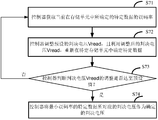
- Step S71 The controller acquires a bit error rate of the specific data currently determined in the storage unit
- Step S72 The controller adjusts the preset decision voltage Vread, and uses the adjusted decision voltage Vread to re-determine the specific data in the specific storage unit;
- the threshold voltage Vth of the memory cell Due to the electronic leakage of the memory cell, only the threshold voltage Vth of the memory cell is shifted to the low voltage direction. Therefore, only the decision voltage Vread can be adjusted to the low voltage direction; for example, the decision voltage Vread of the memory array can be once performed. Adjusting a step size to the low voltage direction, the step size can be specifically 10mv; for example, the original preset decision voltage Vread of the flash memory device is 50mv, then after one adjustment, the decision voltage Vread can be changed to 40mv, and the controller reuses The 40mV decision voltage Vread re-reads specific data in a specific memory unit.
- the 40mv decision voltage Vread can be specifically compared with a specific memory cell threshold voltage Vth when the decision voltage Vread is greater than When the current threshold voltage Vth is current, it is determined that the data stored in the specific storage unit is "1", otherwise, the data stored in the specific storage unit is determined to be "0".
- Step S73 The controller determines whether the adjustment of the decision voltage Vread reaches a preset value, if so, proceeds to step S74; if not, returns to step S71;
- the controller may determine whether the total step size of the adjustment voltage Vread is up to a preset value, and the preset value may be specifically 500mv-600mv; if the decision voltage Vread is adjusted by one step at a time, one step is 10mv, then With the above method, the decision voltage Vread can be adjusted only 50-60 times.
- the controller when the adjustment of the decision voltage Vread does not reach the preset value, the controller will continue to read the specific data in the specific storage unit by using the adjusted decision voltage Vread, assuming that the read is performed.
- Step S74 The controller determines the decision voltage corresponding to the specific data of the minimum bit error rate as the determined decision voltage
- the controller can obtain the specific data read by the different decision voltages Vread by adjusting the decision voltage Vread, and can obtain the error rate of the different specific data.
- the specific In the specific data the specific data with the smallest bit error rate is selected, and the decision voltage Vread corresponding to the specific data with the smallest bit error rate is obtained; finally, the user storage unit is read by the decision voltage Vread corresponding to the specific data of the minimum bit error rate.
- the user data read by the user storage unit can also minimize the error rate of the read user data, thereby reducing storage. Misjudgment of data.
- the present invention also provides an access method of another flash memory device, which can be specifically applied to a solid state hard disk SSD, and the method is specifically as follows:
- a physical block (Block Info Table) is allocated to each physical block in the SSD storage array, and the number of PEs (rewrite) and the retention time (Retention) of each physical block can be recorded in the table.
- Information such as the number of reads; then set a Calibration Table, which stores the offset of the decision voltage Vread of the SSD storage array with PE, Retention, number of readings, and ambient temperature; among them, BIT and Calibration Table It can be stored in the storage medium of the SSD controller.
- the data written into the SSD is generally subjected to ECC (Error Correcting Code) encoding. Therefore, after the controller acquires the data read by the storage array, , the data needs to be ECC decoded again;
- ECC Error Correcting Code
- the function of the SSD controller may be specifically implemented by a DSP (Digital Signal Processing) unit and an ECC decoding unit; when the controller is to read data of the storage array, the SSD controller
- the DSP unit can first obtain the temperature information of the environment, and the temperature sensor is set in the SSD to collect the temperature of the environment in which the SSD is located; then, the physical block that needs to read the data is determined, and the BIT of the current physical block is determined, from the BIT.
- the temperature sensor and the controller inside the SSD are both in the power down state, and the devices cannot operate, and the corresponding SSD controller cannot record the duration of the power-off, and The change in temperature. Therefore, after the SSD is powered on again, information such as temperature information and retention time during the power-off period cannot be obtained; since the above two key parameter information cannot be known, the offset of the decision voltage queried in the Calibration Table will be caused. The value is not accurate, and eventually the error rate of the data read by the offset value is too large. In practical applications, the applicant found that after the SSD is powered off for a long time, after the power is turned on again, the read data will exceed the error correction capability of the ECC, which will result in the inability to obtain accurate stored data.
- the present invention provides another method for accessing a flash memory device, and the method can be specifically applied to a case where the SSD solid state hard disk is powered off for a long time and is powered on again. As shown in FIG. 9, the method is specifically as follows:
- Step S91 First allocate a part of the physical blocks in the storage array for storing specific data, the physical blocks are not used for storing user data; the remaining physical blocks of the storage array are still used for storing user data;
- a physical block for storing specific data may be referred to as a parameter block
- a physical block for storing user data may be referred to as a data block
- the storage array of the SSD may include A plurality of flash chips may be allocated a physical block of 0.5% as a reference block in each flash chip, and the remaining 99.5% of the parameter blocks are used as data blocks;
- Step S92 The controller of the SSD performs erasing wear on the reference block to keep the number of erasures of the reference block consistent with the number of erasing of the data block.
- the SSD performs full disk wear leveling when writing data.
- the controller of the SSD sequentially writes data in the first data block, the second data block, and the third data block, and when erasing data, the controller of the SSD also sequentially erases the first The data block, the second data block, and the data stored in the third data block, so that the number of erasing of the data block tends to be uniform.
- Step S93 The controller of the SSD writes specific data in the reference block and writes specific data in the high reliability storage medium; wherein the high reliability storage medium may be specifically a storage medium in the NOR Flash chip.
- the original specific data or the original user data may be specifically XORed with the white noise random sequence to obtain scrambled specific data, or scrambled user data; in the prior art, white noise is randomly
- the sequence may be specifically generated by a LFSR (Linear Feedback Shift Register), with the Page number as the initial value of the LFSR.
- LFSR Linear Feedback Shift Register
- the scrambling of specific data and user data is mainly to reduce the ICI (Inter-Cell Interference) effect of the flash chip, and the ICI effect refers to storing between different memory cells in the flash chip.
- the phenomenon of mutual interference of data corresponding to the data scrambling described above, after the storage array reads the scrambled specific data or the scrambled user data, the data needs to be descrambled, and the descrambling process may be specifically as follows: The scrambled specific data or the scrambled user data is again XORed with the white noise random sequence to obtain the original specific data or the original user data.
- Step S94 The controller of the SSD takes specific data in the reference block
- Step S95 The controller of the SSD compares the acquired specific data with the specific data stored in the high reliability storage medium, and calculates the bit error rate.
- Step S96 The SSD controller adjusts the decision voltage value of the storage array to a low level direction by using an interface command of the storage array; one step may be specifically 10 mv.
- the interface command can be specifically used to adjust the decision voltage of the storage array.
- the threshold level of the memory cell in the SSD is only shifted to the low voltage direction during the power-down period of the SSD, it is only necessary to adjust the decision voltage of the memory array to the low voltage direction.
- Step S97 The controller of the SSD determines whether the total offset of the decision voltage reaches the maximum offset value, and if not, returns to step S94; otherwise, performs step S98; wherein, the maximum offset value may be specifically about 500-900 mV;
- the SSD controller will continue to adjust the offset value of the read decision voltage voltage according to the above step size, and repeatedly perform steps S94-S96 to calculate the bit error rate of the specific data under each of the decision voltage offset values until the decision voltage is reached.
- the maximum offset value so far.
- Step S98 Acquire an offset voltage corresponding to the specific data with the smallest bit error rate.
- the controller of the SSD can read and write in response to the computer at this time, and after the SSD is powered on, the offset voltage is used to read the stored data to adjust the decision voltage; After the SSD is powered on, the read data is read. Since the Retention time of the stored data is available at this time, the offset level can be specifically queried according to the method disclosed in Embodiment 4, and then the decision voltage adjusted based on the offset level is adjusted. Perform data reading.
- the factors affecting the threshold voltage Vth shift of the memory cell are disclosed in the fourth embodiment, there are factors such as PE, Retention duration, number of readings, and ambient temperature, but the two most important threshold voltage Vth offsets are determined.
- the factors are the number of PEs and the length of Retention.
- by abrading the reference block it can be ensured that the reference block is consistent with the number of PEs of the data block; and since the SSD is powered off for a long time, the specific data of the parameter block and the user data of the data block are both In the comparison of the length of the retention time, the difference between the two can be almost ignored.
- the parameter block is worn to ensure the threshold voltage Vth of the reference block and the data block are biased.
- the phase shift is consistent.
- the method provided in the fourth embodiment can be used to adjust the decision voltage of the storage array.
- the method in the embodiment of the present invention can solve the problem due to the SSD.
- the storage unit error is too high after power-off, which causes the storage data to be unrecoverable.
- the present invention also provides an access method of another flash memory device, the flash memory device including a controller and a storage array, the storage array including a specific storage unit for storing specific data, and a user storage unit for storing the user Data, specific data is used to determine the decision voltage Vread for reading user data, as follows:
- the controller acquires a current threshold voltage Vth of a specific memory cell, and an original threshold voltage Vth, which is a threshold voltage Vth of a specific memory cell when writing specific data;
- the controller determines the decision voltage Vread according to the current threshold voltage Vth of the specific memory cell and the original threshold voltage Vth;
- the controller may determine the offset of the storage unit threshold voltage Vth according to the current threshold voltage Vth and the original threshold voltage Vth of the specific storage unit, and then offset the preset decision voltage Vread according to the offset.
- the specific data stored by a specific memory cell is 0, and the original threshold voltage Vth of the specific memory cell is 5V.
- the quantity can be as shown in Figure 4.
- a specific storage unit may include a plurality of storage elements.
- each storage element in which a charge leak occurs in a specific storage unit may be first determined (executed by SLC, that is, a storage state)
- the threshold voltage Vth offset of the storage element of "0" is calculated, and then the average value of the threshold voltage Vth offset of the storage cells is calculated, and the average value may be specifically determined by the arithmetic average method or the weighted average method in the prior art; Finally, the value of the decision voltage Vread is shifted according to the above average value.
- the probability distribution of the specific data threshold voltage Vth may be pre-stored in the controller.
- the probability distribution of the threshold voltage Vth storing the data “0” is as shown in FIG.
- the right graph of 1 is shown, and the probability distribution of the threshold voltage Vth for storing the data "1" is as shown in the left diagram of FIG.
- the offset amount of the threshold voltage Vth of the specific memory cell is determined; regarding how to calculate the offset amount of the threshold voltage Vth, the above description may be specifically referred to;
- the offset amount of the currently calculated threshold voltage Vth is correspondingly offset from the probability distribution of the entire threshold voltage Vth, and the decision voltage Vread is determined according to the probability distribution of the threshold voltage Vth after the offset; for example, as shown in the figure 5, when it is determined that the threshold value of the threshold voltage Vth of a specific memory cell is 3V, the probability distribution of the entire threshold voltage Vth is also shifted to the left by 3V, and finally, the threshold voltage Vth after the offset is determined.
- the minimum threshold voltage Vth in the case of the probability distribution; the decision voltage Vread may be set to be any value larger than the minimum threshold voltage Vth.
- the controller reads the user data stored in the user storage unit using the determined decision voltage Vread.
- the decision voltage Vread can be determined according to the real-time offset condition of the threshold voltage Vth of the memory cell, so that the misjudgment of the data stored in the memory unit can be reduced.
- the present invention further provides an access device for a flash memory device, the flash memory device at least comprising a storage array, the storage array comprising a specific storage unit and a user storage unit, the specific storage unit for storing specific data, and the user storage unit For storing user data, the specific data is used to determine a decision voltage for reading user data.
- the access device 10 of the flash memory device includes at least: a reading unit 101 for reading specific data stored in a specific storage unit.
- the determining unit 102 is configured to determine a decision voltage according to the read specific data
- the reading unit 101 is further configured to read the user data stored in the user storage unit by using the determined decision voltage.
- the reading unit 101 when reading the specific data stored in the specific storage unit, is specifically configured to: acquire a current threshold voltage of the specific storage unit; compare the preset determination voltage with a current threshold voltage of the specific storage unit, and determine the specific The specific data stored in the storage unit.
- the determining unit 102 is specifically configured to: calculate a bit error rate of the determined specific data; when the bit error rate is less than a preset threshold, use the preset decision voltage as the determined decision voltage.
- the reading unit 101 when there are at least two preset decision voltages, when reading the specific data stored in the specific storage unit, the reading unit 101 is specifically configured to: compare each preset decision voltage with a current threshold voltage of the specific storage unit, Determining the specific data stored in the specific storage unit; the determining unit 102 is specifically configured to: calculate a bit error rate of the specific data determined according to each preset decision; and select a preset decision voltage corresponding to the determined specific data with the smallest bit error rate As a determined decision voltage.
- the determining unit 102 when determining the error rate of the determined specific data, is specifically configured to: compare the determined specific data with the recorded original specific data, and obtain a bit error rate of the determined specific data.
- the access device 10 of the flash memory device may further include: a wear unit configured to perform a wear operation on the specific storage unit according to the wear characteristic of the user storage unit to match the wear characteristics of the specific storage unit and the user storage unit.
- Rewrite unit for rewriting specific data when writing user data to the user storage unit Into a particular storage unit to match the duration characteristics of the particular storage unit and the user storage unit storing the data.
- the storage array is divided into a specific storage unit and a user storage unit in advance, and the storage characteristics of the specific storage unit and the user storage unit are consistent, and the threshold voltages Vth of the two are consistent with each other.
- the decision voltage Vread used by the two tends to be consistent; in the embodiment of the present invention, whenever the user data in the user storage unit is read, the controller reads the specific data stored in the specific storage unit, and according to the Reading the specific data, determining the decision voltage Vread, and finally, using the determined decision voltage Vread, reading the user data stored in the user storage unit; since the threshold voltage Vth offset of the specific memory unit and the user memory unit tends to be the same, The reading of the stored data of the user memory cell by the decision voltage Vread determined in the specific memory cell can reduce the misjudgment of the stored data due to the offset of the threshold voltage Vth.
- the present invention further provides an access device for a flash memory device, the flash memory device at least comprising a storage array, the storage array comprising a specific storage unit and a user storage unit, the specific storage unit for storing specific data, and the user storage unit
- the user data is stored, the specific data is used to determine a decision voltage for reading the user data
- the device includes: an obtaining unit, configured to acquire a current threshold voltage of the specific storage unit, and an original threshold voltage, where the original threshold voltage is specific when the specific data is written a threshold voltage of the storage unit; a decision voltage determining unit, configured to determine a decision voltage according to a current threshold voltage and an original threshold voltage of the specific storage unit; and a user data reading unit configured to read the user storage unit by using the determined decision voltage Stored user data.
- the decision voltage Vread can be determined according to the real-time offset condition of the threshold voltage Vth of the memory cell, so that the misjudgment of the data stored in the memory unit can be reduced.
- the present invention further provides an access system of a flash memory device, as shown in FIG. 11, the access system 11 of the flash memory device includes an access device 111 of the flash memory device and a storage array 112;
- the storage array 112 includes a specific storage unit for storing specific data, a user storage unit for storing user data, and specific data for determining a decision voltage for reading user data;
- the access device 111 of the flash memory device is configured to: read specific data stored in a specific storage unit; determine a decision voltage according to the read specific data; and read user data stored in the user storage unit by using the determined decision voltage;
- the access device 111 of the flash memory device is configured to: acquire a current threshold voltage of a specific storage unit, and an original threshold voltage, the threshold voltage of the specific storage unit when the specific data is written; according to the current threshold voltage of the specific storage unit and The original threshold voltage determines the decision voltage; the user data stored in the user storage unit is read using the determined decision voltage.
- the storage unit of the storage array is divided into a specific storage unit and a user storage unit in advance, and the storage characteristics of the specific storage unit and the user storage unit are consistent, and the threshold voltage Vth of the two is offset. Consistently, the decision voltage Vread used by the two tends to be consistent; in the embodiment of the present invention, the controller reads the specific data stored in the specific storage unit whenever the user data in the user storage unit is read.
- the present invention further provides a readable medium comprising instructions for executing, when the processor of the memory controller executes the execution instruction, the memory controller executes the method for accessing the flash memory device disclosed in the above embodiment.
- the present invention also discloses a memory controller, as shown in FIG. 12, the memory controller 12 includes: a processor 121, a memory 122 and a bus 123;
- the memory 122 is for storing execution instructions
- the processor 121 is connected to the memory 122 via the bus 123, and when the memory controller is running, the processor 121 executes the execution instructions stored by the memory 122 to cause the memory controller to execute:
- the user data stored in the user storage unit is read using the determined decision voltage.
- the storage unit of the storage array is divided into a specific storage unit and a user storage unit in advance, and the storage characteristics of the specific storage unit and the user storage unit are consistent, and the threshold voltage Vth of the two is offset. Consistently, the decision voltage Vread used by the two tends to be consistent; in the embodiment of the present invention, the controller reads the specific data stored in the specific storage unit whenever the user data in the user storage unit is read.
- embodiments of the present invention can be provided as a method, system, or computer program product. Accordingly, the present invention may take the form of an entirely hardware embodiment, an entirely software embodiment, or a combination of software and hardware. Moreover, the invention can take the form of a computer program product embodied on one or more computer-usable storage media (including but not limited to disk storage, CD-ROM, optical storage, etc.) including computer usable program code.
- computer-usable storage media including but not limited to disk storage, CD-ROM, optical storage, etc.
- the computer program instructions can also be stored in a computer readable memory that can direct a computer or other programmable data processing device to operate in a particular manner, such that the instructions stored in the computer readable memory include instructions.
- An article of manufacture of a device that implements the functions specified in a block or blocks of a flow or a flow and/or block diagram of the flowchart.
- These computer program instructions can also be loaded onto a computer or other programmable data processing device such that a series of operational steps are performed on a computer or other programmable device to produce computer-implemented processing for execution on a computer or other programmable device.
- the instructions provide steps for implementing the functions specified in one or more of the flow or in a block or blocks of a flow diagram.
Landscapes
- Engineering & Computer Science (AREA)
- Theoretical Computer Science (AREA)
- Physics & Mathematics (AREA)
- General Engineering & Computer Science (AREA)
- General Physics & Mathematics (AREA)
- Human Computer Interaction (AREA)
- Computer Security & Cryptography (AREA)
- Quality & Reliability (AREA)
- Techniques For Improving Reliability Of Storages (AREA)
- Read Only Memory (AREA)
Abstract
A method, apparatus and system for accessing a flash memory device, said flash memory device comprising a controller and a storage array. Said method comprises: dividing a storage array element into a specific storage unit and a user storage unit (S21); rendering storage characteristics of the specific storage unit to be consistent with those of the user storage unit (S22); the controller writing specific data into the specific storage unit (S23); the controller reading said specific data stored in the specific storage unit (S24); the controller determining a decision voltage Vread according to said specific data which is read (S25); the controller using the determined decision voltage Vread to read user data stored within the user storage unit (S26). By using said access method, apparatus and system, instances wherein data stored on a flash memory device is misjudged may be reduced.
Description
本发明涉及数据存储技术领域,尤其涉及一种闪存设备的访问方法、装置和系统。The present invention relates to the field of data storage technologies, and in particular, to a method, an apparatus, and a system for accessing a flash memory device.
闪存设备是一种长寿命的非易失性存储阵列,即使断电其所存储的数据也不会丢失。由于闪存设备的非易失存储特性和高速读写性能,近年来被广泛应用。A flash device is a long-lived, non-volatile storage array that will not lose data even if it is powered down. Due to the non-volatile storage characteristics and high-speed read and write performance of flash memory devices, they have been widely used in recent years.
在实际应用中,闪存设备的最小存储单位为存储元,而数据在存储元中是以电子的形式存储的,且不同的数据,在存储元中表现为不同的阈值电压Vth;比如,在单阶存储元(SLC,Single-level cell)类型的存储阵列中,每个存储元存储一比特的数据,所存储的数据为0或1;其中,如图1所示,在存储元存储数据1时,其Vth的概率分布如图1中的左边图形所示,而在存储元存储数据0时,其Vth的概率分布如图1中的右边图形所示。在现有技术中,闪存设备的控制器通常采用下述方式,读取存储元中的存储数据:首先获取该存储元的阈值电压Vth,然后将预设的判决电压Vread与该存储元的阈值电压Vth作比较;在判决电压Vread大于存储单元的阈值电压Vth时,确定该存储元存储的数据为“1”;在判决电压Vread小于该存储元的阈值电压Vth时,确定该存储单元存储的数据为“0”。In practical applications, the minimum storage unit of the flash memory device is a storage element, and the data is stored in an electronic form in the storage element, and different data is represented by different threshold voltages Vth in the storage element; for example, in a single In a SLC (Single-level cell) type storage array, each storage element stores one bit of data, and the stored data is 0 or 1; wherein, as shown in FIG. 1, the storage element stores data 1 The probability distribution of Vth is shown in the left graph in Fig. 1, and when the storage unit stores data 0, the probability distribution of Vth is as shown in the right graph in Fig. 1. In the prior art, the controller of the flash memory device generally reads the stored data in the storage element by first acquiring the threshold voltage Vth of the storage element, and then setting the predetermined decision voltage Vread and the threshold of the storage element. The voltage Vth is compared; when the decision voltage Vread is greater than the threshold voltage Vth of the memory cell, determining that the data stored by the memory cell is "1"; when the decision voltage Vread is less than the threshold voltage Vth of the memory cell, determining the storage of the memory cell The data is "0".
但是,在实际应用中,由于存储元中的电子会随着时间的推移而泄漏,而在电子泄露后存储元的阈值电压也会向低电压方向偏移,如此,采用上述方法,对于存储数据0的存储元,当其阈值电压Vth偏移到低于预设的判决电压Vread时,将会造成该存储元存储数据的误判;比如,仍参照图1,一存储元所存储的数据为0,其初始Vth为5V,而经过一段时间后,由于该存储元的电子泄露,其阈值电压Vth变为2V,而预设的判决电压Vread为3V,那么此时,如果采用上述方法,由于此时判决电压Vread(3V)大于阈值电压Vth(2V),闪存设备的控制器将会将该存储元所存储的数据误判为1。However, in practical applications, since the electrons in the memory cell leak over time, the threshold voltage of the memory cell is shifted to the low voltage direction after the electron leakage, and thus, the above method is used to store the data. The storage element of 0, when its threshold voltage Vth is shifted below the preset decision voltage Vread, will cause misjudgment of the storage data stored by the storage element; for example, still referring to FIG. 1, the data stored by a storage element is 0, its initial Vth is 5V, and after a period of time, due to the electronic leakage of the memory element, its threshold voltage Vth becomes 2V, and the preset decision voltage Vread is 3V, then at this time, if the above method is adopted, At this time, the decision voltage Vread (3V) is greater than the threshold voltage Vth (2V), and the controller of the flash memory device will misjudge the data stored in the memory cell as 1.
发明内容Summary of the invention
本发明实施例提供一种闪存设备的访问方法、装置和系统,以减少对闪存设备存储数据的误判。Embodiments of the present invention provide a method, an apparatus, and a system for accessing a flash memory device to reduce misjudgment of data stored in the flash memory device.
第一方面,本发明提供一种闪存设备的访问方法,该闪存设备包括控制器和存储阵列,该存储阵列包括特定存储单元和用户存储单元,其中,特定存储单元用于存储特定数据,用户存储单元用于存储用户数据,特定数据用于确定读取用户数据的判决电压,该方法包括:控制器读取特定存储单元中存储的特定数据,根据读取的特定数据,确定判决电压,以及利用确定的判决电压,读取用户存储单元中存储的用户数据。In a first aspect, the present invention provides a method for accessing a flash memory device, the flash memory device including a controller and a storage array, the storage array including a specific storage unit and a user storage unit, wherein the specific storage unit is configured to store specific data, and the user stores The unit is configured to store user data, and the specific data is used to determine a decision voltage for reading the user data, the method comprising: the controller reading the specific data stored in the specific storage unit, determining the decision voltage according to the read specific data, and utilizing The determined decision voltage reads the user data stored in the user storage unit.
在本发明实施例中,预先将存储阵列分为特定存储单元和用户存储单元,且特定存储单元和用户存储单元的存储特性相一致,两者的阈值电压Vth偏移相一致,从而两者所采用的判决电压Vread趋于一致;而本发明实施例中,每当在读取用户存储单元中的用户数据时,所述控制器读取特定存储单元中存储的特定数据,且根据所读取的特定数
据,确定判决电压Vread,最后,利用确定的判决电压Vread,读取用户存储单元中存储的所述用户数据;由于特定存储单元和用户存储单元的阈值电压Vth偏移趋于一致,因此,利用在特定存储单元中确定的判决电压Vread对用户存储单元的存储数据进行读取,可减少由于阈值电压Vth的偏移,而造成的存储数据的误判。In the embodiment of the present invention, the storage array is divided into a specific storage unit and a user storage unit in advance, and the storage characteristics of the specific storage unit and the user storage unit are consistent, and the threshold voltages Vth of the two are consistent with each other, so that both The decision voltage Vread used tends to be consistent; in the embodiment of the present invention, whenever the user data in the user storage unit is read, the controller reads the specific data stored in the specific storage unit, and according to the read Specific number
According to the determination of the decision voltage Vread, finally, the user data stored in the user storage unit is read by using the determined decision voltage Vread; since the threshold voltage Vth offset of the specific memory unit and the user memory unit tends to be consistent, therefore, The decision voltage Vread determined in the specific memory cell reads the stored data of the user memory cell, which can reduce the misjudgment of the stored data due to the offset of the threshold voltage Vth.
结合第一方面,在第一种可能的实现方式中,控制器读取特定存储单元中存储的特定数据,包括:控制器获取特定存储单元的当前阈值电压、比较预设判决电压与特定存储单元的当前阈值电压,确定特定存储单元中存储的特定数据。在本发明实施例中,可获取特定存储单元中所存储的特定数据。With reference to the first aspect, in a first possible implementation, the controller reads the specific data stored in the specific storage unit, including: the controller acquires a current threshold voltage of the specific storage unit, compares the preset determination voltage, and the specific storage unit The current threshold voltage determines the specific data stored in a particular memory location. In the embodiment of the present invention, specific data stored in a specific storage unit can be acquired.
结合第一方面的第一种可能的实现方式,在第二种可能的实现方式中,控制器根据读取的特定数据,确定判决电压,包括:控制器计算确定的特定数据的误码率,在误码率小于预设阈值时,将预设判决电压作为确定的判决电压。With reference to the first possible implementation manner of the first aspect, in a second possible implementation manner, the controller determines, according to the specific data that is read, the determining voltage, that is, the controller calculates the error rate of the determined specific data, When the bit error rate is less than the preset threshold, the preset decision voltage is taken as the determined decision voltage.
在本发明实施例中,可获取误码率小于预设阈值的特定数据,然后,利用误码率小于预设阈值的特定数据所对应的判决电压Vread,在用户存储单元中读取用户数据,可使得所读取的用户数据的误码率也小于预设阈值,从而减少对存储数据的误判。In the embodiment of the present invention, the specific data whose bit error rate is less than the preset threshold is obtained, and then the user data is read in the user storage unit by using the decision voltage Vread corresponding to the specific data whose bit error rate is less than the preset threshold. The error rate of the read user data can also be made smaller than a preset threshold, thereby reducing misjudgment of the stored data.
结合第一方面的第一种可能的实现方式,在第三种可能的实现方式中,预设判决电压有至少两个;控制器比较预设判决电压与特定存储单元的当前阈值电压,确定特定存储单元中存储的特定数据,包括:控制器比较每个预设判决电压与特定存储单元的当前阈值电压,确定特定存储单元中存储的特定数据;控制器根据读取的特定数据,确定判决电压,包括:控制器计算根据每个预设判决确定的特定数据的误码率,选择误码率最小的确定的特定数据对应的预设判决电压作为确定的判决电压。With reference to the first possible implementation manner of the first aspect, in a third possible implementation manner, the preset determination voltage has at least two; the controller compares the preset determination voltage with a current threshold voltage of the specific storage unit, and determines the specific The specific data stored in the storage unit includes: the controller compares each preset decision voltage with a current threshold voltage of the specific storage unit, and determines specific data stored in the specific storage unit; and the controller determines the decision voltage according to the read specific data. The controller includes: calculating a bit error rate of the specific data determined according to each preset decision, and selecting a predetermined decision voltage corresponding to the determined specific data with the smallest bit error rate as the determined decision voltage.
在本发明实施例中,利用误码率最小的特定数据所对应的判决电压,在用户存储单元中读取用户数据,可使所读取的用户数据的误码率也最小,从而减少对存储数据的误判。In the embodiment of the present invention, by using the decision voltage corresponding to the specific data with the smallest bit error rate, the user data is read in the user storage unit, so that the error rate of the read user data is also minimized, thereby reducing the storage. Misjudgment of data.
结合第一方面的第二种可能的实现方式或第一方面的第三种可能的实现方式,在第四种可能的实现方式中,控制器计算确定的特定数据的误码率包括:控制器比较确定的特定数据和记录的原始特定数据,获得确定的特定数据的误码率。在本发明实施例中,可确定特定数据的误码率。With reference to the second possible implementation of the first aspect or the third possible implementation of the first aspect, in a fourth possible implementation, the controller calculates the error rate of the determined specific data, including: the controller Comparing the determined specific data with the original specific data of the record, the bit error rate of the determined specific data is obtained. In an embodiment of the invention, the bit error rate of a particular data can be determined.
结合第一方面、第一方面的第一种可能的实现方式、第一方面的第二种可能的实现方式、第一方面的第三种可能的实现方式或第一方面的第四种可能的实现方式,在第五种可能的实现方式中,上述方法还包括:控制器根据用户存储单元的磨损特性对特定存储单元进行磨损操作,以使特定存储单元和用户存储单元的磨损特性相一致。在本发明实施例中,可使特定存储单元和用户存储单元的磨损特性相一致。Combining the first aspect, the first possible implementation of the first aspect, the second possible implementation of the first aspect, the third possible implementation of the first aspect, or the fourth possible aspect of the first aspect In a fifth possible implementation manner, the method further includes: the controller performing a wear operation on the specific storage unit according to the wear characteristic of the user storage unit, so that the wear characteristics of the specific storage unit and the user storage unit are consistent. In an embodiment of the invention, the wear characteristics of a particular memory unit and a user memory unit may be matched.
结合第一方面、第一方面的第一种可能的实现方式、第一方面的第二种可能的实现方式、第一方面的第三种可能的实现方式或第一方面的第四种可能的实现方式,在第六种可能的实现方式中,上述方法还包括:控制器在将用户数据写入至用户存储单元时,同步将特定数据重新写入至特定存储单元,以使得特定存储单元和用户存储单元存储数据的时长特性相一致。在本发明实施例中,可使特定存储单元和用户存储单元存储数据的时长特性相一致。Combining the first aspect, the first possible implementation of the first aspect, the second possible implementation of the first aspect, the third possible implementation of the first aspect, or the fourth possible aspect of the first aspect In a sixth possible implementation manner, the method further includes: when the controller writes the user data to the user storage unit, synchronously rewriting the specific data to the specific storage unit, so that the specific storage unit and The duration characteristics of the user storage unit storing data are consistent. In the embodiment of the present invention, the duration characteristics of the data stored by the specific storage unit and the user storage unit may be consistent.
第二方面,本发明提供一种闪存设备的访问方法,该闪存设备包括控制器和存储阵
列,该存储阵列包括特定存储单元和用户存储单元,其中,特定存储单元用于存储特定数据,用户存储单元用于存储用户数据,特定数据用于确定读取用户数据的判决电压,该方法包括:控制器获取特定存储单元的当前阈值电压,以及原始阈值电压,根据特定存储单元的当前阈值电压和原始阈值电压,确定判决电压,以及利用确定的判决电压,读取用户存储单元中存储的用户数据,其中,原始阈值电压为写入特定数据时特定存储单元的阈值电压。In a second aspect, the present invention provides a method for accessing a flash memory device including a controller and a memory array
a column, the storage array comprising a specific storage unit for storing specific data, a user storage unit for storing user data, and specific data for determining a decision voltage for reading user data, the method comprising : the controller acquires a current threshold voltage of the specific memory cell, and an original threshold voltage, determines a decision voltage according to a current threshold voltage of the specific memory cell and the original threshold voltage, and reads the user stored in the user storage unit by using the determined decision voltage Data, where the original threshold voltage is the threshold voltage of a particular memory cell when particular data is written.
由上可见,在本发明实施例中,采用上述方法,可根据存储单元阈值电压Vth的实时偏移情况,确定判决电压Vread,从而可减少对存储单元存储数据的误判。It can be seen that, in the embodiment of the present invention, by using the above method, the decision voltage Vread can be determined according to the real-time offset condition of the threshold voltage Vth of the memory cell, so that the misjudgment of the data stored in the memory unit can be reduced.
第三方面,本发明提供一种闪存设备的访问装置,闪存设备至少包括存储阵列,该存储阵列包括特定存储单元和用户存储单元,其中,特定存储单元用于存储特定数据,用户存储单元用于存储用户数据,特定数据用于确定读取用户数据的判决电压,该装置包括:读取单元和确定单元,其中,读取单元,用于读取特定存储单元中存储的特定数据以及利用确定的判决电压,读取用户存储单元中存储的用户数据,确定单元,用于根据读取的特定数据,确定判决电压。采用本发明的装置,可减少对存储单元存储数据的误判。In a third aspect, the present invention provides an access device for a flash memory device, the flash memory device including at least a storage array including a specific storage unit and a user storage unit, wherein the specific storage unit is configured to store specific data, and the user storage unit is used for Storing user data, the specific data is used to determine a decision voltage for reading user data, the apparatus comprising: a reading unit and a determining unit, wherein the reading unit is configured to read specific data stored in the specific storage unit and utilize the determined The decision voltage reads the user data stored in the user storage unit, and the determining unit is configured to determine the decision voltage according to the read specific data. With the apparatus of the present invention, misjudgment of data stored in the storage unit can be reduced.
结合第三方面,在第一种可能的实现方式中,读取单元在读取特定存储单元中存储的特定数据时,具体用于:获取特定存储单元的当前阈值电压、比较预设判决电压与特定存储单元的当前阈值电压,确定特定存储单元中存储的特定数据。在本发明实施例中,可在存储单元中确定特定数据。With reference to the third aspect, in a first possible implementation manner, when reading the specific data stored in the specific storage unit, the reading unit is specifically configured to: acquire a current threshold voltage of the specific storage unit, compare the preset determination voltage, and The current threshold voltage of a particular memory cell determines the particular data stored in a particular memory cell. In an embodiment of the invention, specific data may be determined in the storage unit.
结合第三方面的第一种可能的实现方式,在第二种可能的实现方式中,确定单元,具体用于:计算确定的特定数据的误码率,且在误码率小于预设阈值时,将预设判决电压作为确定的判决电压。With reference to the first possible implementation manner of the third aspect, in a second possible implementation manner, the determining unit is specifically configured to: calculate a bit error rate of the determined specific data, and when the error rate is less than a preset threshold The preset decision voltage is taken as the determined decision voltage.
在本发明实施例中,可获取误码率小于预设阈值的特定数据,然后,利用误码率小于预设阈值的特定数据所对应的判决电压Vread,在用户存储单元中读取用户数据,从而使所读取的用户数据的误码率也小于预设阈值,进而减少对存储数据的误判。In the embodiment of the present invention, the specific data whose bit error rate is less than the preset threshold is obtained, and then the user data is read in the user storage unit by using the decision voltage Vread corresponding to the specific data whose bit error rate is less than the preset threshold. Therefore, the error rate of the read user data is also less than a preset threshold, thereby reducing misjudgment of the stored data.
结合第三方面的第一种可能的实现方式,在第三种可能的实现方式中,预设判决电压有至少两个,读取单元在读取特定存储单元中存储的特定数据时,具体用于:比较每个预设判决电压与特定存储单元的当前阈值电压,确定特定存储单元中存储的特定数据;确定单元,具体用于:计算根据每个预设判决确定的特定数据的误码率、选择误码率最小的确定的特定数据对应的预设判决电压作为确定的判决电压。With reference to the first possible implementation manner of the third aspect, in a third possible implementation manner, the preset determination voltage has at least two, and the reading unit uses the specific data stored in the specific storage unit. And: comparing each preset decision voltage with a current threshold voltage of the specific storage unit to determine specific data stored in the specific storage unit; and determining unit, specifically configured to: calculate a bit error rate of the specific data determined according to each preset decision And selecting a preset decision voltage corresponding to the determined specific data with the smallest bit error rate as the determined decision voltage.
在本发明实施例中,利用误码率最小的特定数据所对应的判决电压,在用户存储单元中读取用户数据,可使所读取的用户数据的误码率也最小,从而减少对存储数据的误判。In the embodiment of the present invention, by using the decision voltage corresponding to the specific data with the smallest bit error rate, the user data is read in the user storage unit, so that the error rate of the read user data is also minimized, thereby reducing the storage. Misjudgment of data.
结合第三方面的第二种可能的实现方式或第三方面的第三种可能的实现方式,在第四种可能的实现方式中,确定单元在计算确定的特定数据的误码率时,具体用于:比较确定的特定数据和记录的原始特定数据,获得确定的特定数据的误码率。在本发明实施例中,可确定特定数据的误码率。With reference to the second possible implementation manner of the third aspect or the third possible implementation manner of the third aspect, in a fourth possible implementation manner, the determining unit, when calculating the bit error rate of the determined specific data, specifically For: comparing the determined specific data with the original specific data of the record, and obtaining the bit error rate of the determined specific data. In an embodiment of the invention, the bit error rate of a particular data can be determined.
结合第三方面、第三方面的第一种可能的实现方式、第三方面的第二种可能的实现方式、第三方面的第三种可能的实现方式或第三方面的第四种可能的实现方式,在第五
种可能的实现方式中,该装置还包括:磨损单元,用于根据用户存储单元的磨损特性对特定存储单元进行磨损操作,以使特定存储单元和用户存储单元的磨损特性相一致。在本发明实施例中,可使得特定存储单元和用户存储单元的磨损特性相一致。With reference to the third aspect, the first possible implementation of the third aspect, the second possible implementation of the third aspect, the third possible implementation of the third aspect, or the fourth possible aspect of the third aspect Implementation, in the fifth
In a possible implementation manner, the apparatus further includes: a wear unit configured to perform a wear operation on the specific storage unit according to the wear characteristic of the user storage unit to match the wear characteristics of the specific storage unit and the user storage unit. In an embodiment of the invention, the wear characteristics of a particular memory unit and a user memory unit may be made consistent.
结合第三方面、第三方面的第一种可能的实现方式、第三方面的第二种可能的实现方式、第三方面的第三种可能的实现方式或第三方面的第四种可能的实现方式,在第六种可能的实现方式中,该装置还包括:重写入单元,用于在将用户数据写入至用户存储单元时,同步将特定数据重新写入至特定存储单元,以使得特定存储单元和用户存储单元存储数据的时长特性相一致。在本发明实施例中,可使得特定存储单元和用户存储单元存储数据的时长特性相一致。With reference to the third aspect, the first possible implementation of the third aspect, the second possible implementation of the third aspect, the third possible implementation of the third aspect, or the fourth possible aspect of the third aspect In a sixth possible implementation manner, the apparatus further includes: a rewriting unit, configured to rewrite the specific data to the specific storage unit when the user data is written to the user storage unit, to The duration characteristics of the data stored by the particular storage unit and the user storage unit are made consistent. In the embodiment of the present invention, the duration characteristics of the data stored by the specific storage unit and the user storage unit may be made consistent.
第四方面,本发明提供一种闪存设备的访问装置,该闪存设备包括存储阵列,该存储阵列包括特定存储单元和用户存储单元,其中,特定存储单元用于存储特定数据,用户存储单元用于存储用户数据,特定数据用于确定读取用户数据的判决电压,该装置包括:获取单元、判决电压确定单元和用户数据读取单元,其中,获取单元,用于获取特定存储单元的当前阈值电压,以及原始阈值电压,原始阈值电压为写入特定数据时特定存储单元的阈值电压;判决电压确定单元,用于根据特定存储单元的当前阈值电压和原始阈值电压,确定判决电压;用户数据读取单元,用于利用确定的判决电压,读取用户存储单元中存储的用户数据。In a fourth aspect, the present invention provides an access device for a flash memory device, the flash memory device including a storage array including a specific storage unit and a user storage unit, wherein the specific storage unit is configured to store specific data, and the user storage unit is used for Storing user data, the specific data is used to determine a decision voltage for reading the user data, the device comprising: an obtaining unit, a decision voltage determining unit, and a user data reading unit, wherein the obtaining unit is configured to acquire a current threshold voltage of the specific storage unit And an original threshold voltage, the threshold voltage of the specific memory cell when writing the specific data; the decision voltage determining unit, configured to determine the decision voltage according to the current threshold voltage of the specific memory cell and the original threshold voltage; user data reading And means for reading user data stored in the user storage unit by using the determined decision voltage.
由上可见,在本发明实施例中,采用上述方法,可根据存储单元阈值电压Vth的实时偏移情况,确定判决电压Vread,从而减少对存储单元存储数据的误判。It can be seen from the above that in the embodiment of the present invention, by using the above method, the decision voltage Vread can be determined according to the real-time offset condition of the threshold voltage Vth of the memory cell, thereby reducing the misjudgment of the data stored in the memory cell.
第五方面,本发明提供一种闪存设备的访问系统,该系统包括第三方面提供的闪存设备的访问装置和存储阵列;该存储阵列包括特定存储单元和用户存储单元,其中,特定存储单元用于存储特定数据,用户存储单元用于存储用户数据,特定数据用于确定读取用户数据的判决电压;该闪存设备的访问装置具体用于:读取特定存储单元中存储的特定数据,根据读取的特定数据,确定判决电压以及利用确定的判决电压,读取用户存储单元中存储的用户数据;In a fifth aspect, the present invention provides an access system for a flash memory device, the system comprising the access device and the storage array of the flash memory device provided by the third aspect; the storage array includes a specific storage unit and a user storage unit, wherein the specific storage unit is used For storing specific data, the user storage unit is configured to store user data, and the specific data is used to determine a decision voltage for reading the user data; the access device of the flash memory device is specifically configured to: read specific data stored in a specific storage unit, according to the read Taking specific data, determining the decision voltage, and using the determined decision voltage, reading the user data stored in the user storage unit;
或,该系统包括第四方面提供的闪存设备的访问装置和存储阵列;该存储阵列包括特定存储单元和用户存储单元,其中,特定存储单元用于存储特定数据,用户存储单元用于存储用户数据,特定数据用于确定读取用户数据的判决电压;闪存设备的访问装置具体用于:获取特定存储单元的当前阈值电压,以及原始阈值电压,其中,原始阈值电压为写入特定数据时特定存储单元的阈值电压,根据特定存储单元的当前阈值电压和原始阈值电压,确定判决电压,以及利用确定的判决电压,读取用户存储单元中存储的用户数据。采用本发明的系统,可减少对存储数据的误判。Or the system includes the access device and the storage array of the flash device provided by the fourth aspect; the storage array includes a specific storage unit and a user storage unit, wherein the specific storage unit is configured to store specific data, and the user storage unit is configured to store user data The specific data is used to determine a decision voltage for reading the user data; the access device of the flash memory device is specifically configured to: acquire a current threshold voltage of the specific storage unit, and an original threshold voltage, wherein the original threshold voltage is a specific storage when the specific data is written The threshold voltage of the cell determines the decision voltage based on the current threshold voltage of the particular memory cell and the original threshold voltage, and reads the user data stored in the user memory cell using the determined decision voltage. With the system of the present invention, misjudgment of stored data can be reduced.
第六方面,本发明提供一种可读介质,包括执行指令,当存储控制器的处理器执行执行指令时,存储控制器执行第一方面提供的方法或第二方面提供的方法。采用本发明的可读介质,可减少对存储数据的误判。In a sixth aspect, the present invention provides a readable medium comprising executing instructions that, when a processor of a memory controller executes an execution instruction, perform a method provided by the first aspect or a method provided by the second aspect. With the readable medium of the present invention, misjudgment of stored data can be reduced.
第七方面,提供一种存储控制器,该存储控制器包括:处理器、存储器和总线;其中,存储器用于存储执行指令,处理器与存储器通过总线连接,当存储控制器运行时,处理器执行存储器存储的执行指令,以使存储控制器执行第一方面提供的方法或第二方面提供的方法。采用本发明的存储控制器,可减少对存储数据的误判。
According to a seventh aspect, a memory controller is provided, the memory controller includes: a processor, a memory, and a bus; wherein the memory is configured to store execution instructions, the processor is connected to the memory through a bus, and when the memory controller is running, the processor Execution instructions stored in the memory are executed to cause the memory controller to perform the method provided by the first aspect or the method provided by the second aspect. With the memory controller of the present invention, misjudgment of stored data can be reduced.
由上可见,在本发明实施例中,预先将存储阵列分为特定存储单元和用户存储单元,且特定存储单元和用户存储单元的存储特性相一致,两者的阈值电压Vth偏移相一致,从而两者所采用的判决电压Vread趋于一致;而本发明实施例中,每当在读取用户存储单元中的用户数据时,控制器读取特定存储单元中存储的特定数据,且根据所读取的特定数据,确定判决电压Vread,最后,利用确定的判决电压Vread,读取用户存储单元中存储的用户数据;由于特定存储单元和用户存储单元的阈值电压Vth偏移趋于一致,因此,利用在特定存储单元中确定的判决电压Vread对用户存储单元的存储数据进行读取,可减少由于阈值电压Vth的偏移,而造成的对闪存设备存储数据的误判。It can be seen that, in the embodiment of the present invention, the storage array is divided into a specific storage unit and a user storage unit in advance, and the storage characteristics of the specific storage unit and the user storage unit are consistent, and the threshold voltages Vth of the two are consistent with each other. Therefore, the decision voltage Vread used by the two tends to be consistent; in the embodiment of the present invention, whenever the user data in the user storage unit is read, the controller reads the specific data stored in the specific storage unit, and according to the Reading the specific data, determining the decision voltage Vread, and finally, using the determined decision voltage Vread, reading the user data stored in the user storage unit; since the threshold voltage Vth offset of the specific memory unit and the user memory unit tends to be the same, Reading the stored data of the user storage unit by using the decision voltage Vread determined in the specific storage unit can reduce the misjudgment of the data stored in the flash memory device due to the offset of the threshold voltage Vth.
为了更清楚地说明本发明实施例或现有技术中的技术方案,下面将对实施例或现有技术描述中所需要使用的附图作一简单地介绍,显而易见地,下面描述中的附图是本发明的一些实施例,对于本领域普通技术人员来讲,还可以根据这些附图获得其他的附图。In order to more clearly illustrate the embodiments of the present invention or the technical solutions in the prior art, a brief description of the drawings used in the embodiments or the prior art description will be briefly described below. Obviously, the drawings in the following description It is a number of embodiments of the present invention, and other figures may be obtained from those of ordinary skill in the art in view of these drawings.
图1为本发明实施例提供的闪存设备阈值电压的概率分布示意图;1 is a schematic diagram of probability distribution of threshold voltages of a flash memory device according to an embodiment of the present invention;
图2为本发明实施例提供的闪存设备的访问方法的一流程示意图;2 is a schematic flowchart of a method for accessing a flash memory device according to an embodiment of the present invention;
图3为本发明实施例提供的SSD的结构示意图;FIG. 3 is a schematic structural diagram of an SSD according to an embodiment of the present disclosure;
图4为本发明实施例提供的判决电压的调整示意图;4 is a schematic diagram of adjustment of a decision voltage according to an embodiment of the present invention;
图5为本发明实施例提供的确定判决电压的示意图;FIG. 5 is a schematic diagram of determining a decision voltage according to an embodiment of the present invention;
图6为本发明实施例提供的闪存设备的访问方法的另一流程示意图;FIG. 6 is another schematic flowchart of a method for accessing a flash memory device according to an embodiment of the present disclosure;
图7为本发明实施例提供的闪存设备的访问方法的又一流程示意图;FIG. 7 is still another schematic flowchart of a method for accessing a flash memory device according to an embodiment of the present disclosure;
图8为本发明实施例提供的闪存设备的访问方法的另一流程示意图;FIG. 8 is another schematic flowchart of a method for accessing a flash memory device according to an embodiment of the present disclosure;
图9为本发明实施例提供的闪存设备的访问方法的又一流程示意图;FIG. 9 is still another schematic flowchart of a method for accessing a flash memory device according to an embodiment of the present disclosure;
图10为本发明实施例提供的闪存设备的访问装置的一结构示意图;FIG. 10 is a schematic structural diagram of an access device of a flash memory device according to an embodiment of the present disclosure;
图11为本发明实施例提供的闪存设备的访问系统的一结构示意图;FIG. 11 is a schematic structural diagram of an access system of a flash memory device according to an embodiment of the present disclosure;
图12为本发明实施例提供的闪存设备的一结构示意图。FIG. 12 is a schematic structural diagram of a flash memory device according to an embodiment of the present invention.
下面将结合本发明实施例中的附图,对本发明实施例中的技术方案进行清楚、完整地描述,显然,所描述的实施例仅仅是本发明一部分实施例,并不是全部的实施例。The technical solutions in the embodiments of the present invention are clearly and completely described in the following with reference to the accompanying drawings in the embodiments of the present invention. It is obvious that the described embodiments are only a part of the embodiments of the present invention, and not all of the embodiments.
本发明首先提供一种闪存设备的访问方法,该方法的应用场景如下:The present invention first provides an access method for a flash memory device. The application scenario of the method is as follows:
目前,闪存设备主要由两部分构成,分别为控制器和存储阵列,且存储阵列的最小存储单位为存储元;通常,采用下述方法,读取存储元中存储的数据:首先获取存储元的阈值电压Vth,然后将预设的判决电压Vread与存储元的阈值电压Vth作比较;以单阶存储元(SLC,Single-level cell)进行举例说明,SLC是指只记录一位二进制比特位“0”或“1”的存储元,如果判决电压Vread大于存储元的阈值电压Vth,确定该存储元所存储的数据为“1”;如果判决电压Vread小于存储元的阈值电压Vth,确定存储元所存储的数据为“0”。At present, the flash memory device is mainly composed of two parts, namely a controller and a storage array, and the minimum storage unit of the storage array is a storage element; generally, the following method is used to read the data stored in the storage element: firstly, the storage element is obtained. The threshold voltage Vth is then compared with the threshold voltage Vth of the storage element; the single-level cell (SLC) is used to illustrate that the SLC refers to recording only one bit of the binary bit. a storage element of 0" or "1", if the decision voltage Vread is greater than the threshold voltage Vth of the storage element, determining that the data stored by the storage element is "1"; if the decision voltage Vread is less than the threshold voltage Vth of the storage element, determining the storage element The stored data is "0".
由于在实际应用中,数据在存储元中是以电子的形式存在的,而随着时间的推移,存储元中的电子会泄露,阈值电压Vth会向低电压方向偏移,而在现有技术中,存储阵列
以预设的判决电压Vread读取存储数据,将会导致存储元存储数据的误判。比如,一存储元所存储的数据为“0”,其初始阈值电压Vth为5V,而经过一段时间后,由于该存储单元的电子泄露,其阈值电压Vth变为2V,而预设的判决电压Vread为3V,那么此时,如果采用上述方法,由于此时判决电压Vread(3V)大于阈值电压Vth(2V),会将该存储元所存储的数据误判为“1”。In practical applications, data exists in the form of electrons in the storage element, and over time, electrons in the storage element may leak, and the threshold voltage Vth may shift toward a low voltage direction, whereas in the prior art Medium, storage array
Reading the stored data with the preset decision voltage Vread will result in a misjudgment of the storage element storage data. For example, the data stored in a memory cell is “0”, and the initial threshold voltage Vth is 5V. After a period of time, due to the electronic leakage of the memory cell, the threshold voltage Vth becomes 2V, and the preset decision voltage is Vread is 3V. At this time, if the above method is adopted, since the decision voltage Vread (3V) is greater than the threshold voltage Vth (2V) at this time, the data stored in the memory cell is misjudged as "1".
应理解,为了描述方便,本发明实施例仅仅以单阶存储元进行举例说明,但本发明实施例适用多阶存储元(MLC,Multi-level cell),MLC是指可以记录两位或者两位以上的二进制比特位的存储元。It should be understood that, for convenience of description, the embodiment of the present invention is only illustrated by a single-order storage element, but the embodiment of the present invention is applicable to a multi-level cell (MLC), and the MLC refers to two or two bits that can be recorded. The storage element of the above binary bit.
实施例一 Embodiment 1
基于上述应用场景,本发明提供一种闪存设备的访问方法,闪存设备可具体为U盘(USB闪存盘,USB flash disk)和SSD(Solid State Drives,固态硬盘)等设备,闪存设备可具体由控制器和存储阵列组成,控制器的功能可具体由控制芯片实现,存储阵列的功能可具体由存储芯片实现,存储芯片为Flash芯片,Flash类型的芯片可具体为Nand flash芯片;而本发明提供的闪存设备的访问方法,如图2所示,可具体包括以下步骤:Based on the above application scenario, the present invention provides a method for accessing a flash memory device. The flash memory device may be specifically a device such as a USB flash drive (USB flash disk) and an SSD (Solid State Drives). The controller and the storage array are composed of a controller, and the function of the controller may be specifically implemented by a control chip. The function of the storage array may be specifically implemented by a memory chip, the memory chip is a Flash chip, and the Flash type chip may be specifically a Nand flash chip; The access method of the flash memory device, as shown in FIG. 2, may specifically include the following steps:
步骤S21:首先将存储阵列分为特定存储单元和用户存储单元;Step S21: First, the storage array is divided into a specific storage unit and a user storage unit;
其中,特定存储单元具体用于存储特定数据,用户存储单元具体用于存储用户数据,特定数据具体用于确定读取用户数据的判决电压Vread,在本发明实施例中,特定数据可具体为N比特位的二进制数据,特定数据是计算机系统预知的数据,例如,特定数据可以是一个预设的二进制数列,或者计算机系统将特定数据备份在安全性能较高的存储设备中,其中N为大于0的正整数,在以下实施例不再赘述。The specific storage unit is specifically configured to store the specific data, and the user storage unit is specifically configured to store the user data, and the specific data is specifically used to determine the determination voltage Vread for reading the user data. In the embodiment of the present invention, the specific data may be specifically N. The binary data of the bit, the specific data is data predicted by the computer system. For example, the specific data may be a preset binary sequence, or the computer system backs up the specific data in a storage device with high security performance, where N is greater than 0. The positive integers are not described in the following embodiments.
在本发明实施例中,如图3所示,闪存设备的存储阵列可具体包括多个物理块(Block),而每个物理块可包括多个页面(Page),每个页面包括多个存储元。在实际应用中,SSD具体以物理块为单位对存储的数据进行擦除的,SSD具体以页面为单位对存储数据进行读写的。为了方便对特定存储单元存储的特定数据进行擦除操作,可具体在存储阵列的中预留一部分物理块,该物理块中的存储元用于存储特定数据,也即上述特定存储单元可具体包括预留物理块内的一个或多个存储元,而该存储阵列的剩余物理块用于存储用户数据,也即上述用户存储单元可具体包括剩余物理块内的一个或多个存储元。在本发明实施例中,可具体设置存储阵列中0.5%的物理块,用于存储特定数据,99.5%的物理块,用于存储用户数据;In the embodiment of the present invention, as shown in FIG. 3, the storage array of the flash memory device may specifically include a plurality of physical blocks, and each physical block may include multiple pages, each of which includes multiple storages. yuan. In practical applications, the SSD specifically erases the stored data in units of physical blocks, and the SSD reads and writes the stored data in units of pages. In order to facilitate the erasing operation of the specific data stored in the specific storage unit, a part of the physical block may be reserved in the storage array, and the storage element in the physical block is used to store the specific data, that is, the specific storage unit may specifically include the foregoing The one or more storage elements in the physical block are reserved, and the remaining physical blocks of the storage array are used to store user data, that is, the user storage unit may specifically include one or more storage elements in the remaining physical blocks. In the embodiment of the present invention, 0.5% of physical blocks in the storage array may be specifically configured to store specific data, and 99.5% of the physical blocks are used to store user data;
步骤S22:使得特定存储单元和用户存储单元的存储特性相一致;Step S22: making the storage characteristics of the specific storage unit and the user storage unit consistent;
在本发明实施例中,由于决定存储元的阈值电压Vth偏移的主要因素为存储元的磨损特性,也即PE(Program/Erase cycle,擦写次数),和数据的存储时长(Retention)特性;在本发明实施例中,可具体采用以下方式,确保特定存储单元和用户存储单元的磨损特性以及存储数据的时长特性相一致:In the embodiment of the present invention, the main factor determining the threshold voltage Vth of the memory cell is the wear characteristic of the memory element, that is, PE (Program/Erase cycle), and the retention time of the data. In the embodiment of the present invention, the following manner may be specifically adopted to ensure that the wear characteristics of the specific storage unit and the user storage unit and the duration characteristics of the stored data are consistent:
应理解,因为闪存设备以物理块为单位进行擦除操作,且不同物理的PE次数可能不相同,可以将存储用户数据的物理块分为多个用户存储单元,每个用户存储单元分别有一个特定存储单元与其相对应,即用户存储单元和特定存储单元都可以分别有多个,用户存储单元与特定存储单元存在对应关系,相互对应的用户存储单元和特定存储单元的
存储特性相一致。且用户存储单元与特定存储之间的对应关系可以动态调整。为了介绍方便,除非另有说明,以下描述中的用户存储单元与特定存储单元相互对应。It should be understood that, since the flash device performs an erase operation in units of physical blocks, and the number of PEs of different physical sources may be different, the physical block storing the user data may be divided into a plurality of user storage units, and each user storage unit has one. A specific storage unit corresponding thereto, that is, a user storage unit and a specific storage unit may each have a plurality of, a user storage unit has a corresponding relationship with a specific storage unit, a corresponding user storage unit and a specific storage unit
The storage characteristics are consistent. And the correspondence between the user storage unit and the specific storage can be dynamically adjusted. For convenience of description, the user storage unit in the following description corresponds to a specific storage unit unless otherwise stated.
控制器根据用户存储单元的磨损特性对特定存储单元进行磨损操作,以使特定存储单元和用户存储单元的磨损特性相一致,磨损操作包括对特定存储单元所存储的特定数据擦除的操作以及将特定数据重新写入特定存储单元的操作。The controller performs a wear operation on the specific storage unit according to the wear characteristics of the user storage unit to match the wear characteristics of the specific storage unit and the user storage unit, the wear operation includes the operation of erasing the specific data stored by the specific storage unit, and The operation of rewriting specific data to a specific storage unit.
可选的,控制器可每间隔预设时长,获取一次用户存储单元的擦写次数;擦写次数可具体为用户存储单元被擦除存储数据的次数;用户存储单元可具体记录自身的擦写次数,具体可当每次用户存储单元被擦除一次数据时,计数增加1;而在控制器获取上述擦写次数后;控制器对特定存储单元进行同样次数的擦写操作;比如,控制器获取的擦写次数为M,控制器可具体对特定存储单元存储的特定数据进行M次擦除操作,然后再将特定数据写入至特定存储单元,其中M为大于0的正整数。Optionally, the controller may obtain the number of times of erasing and writing of the user storage unit every preset time interval; the number of times of erasing may be specifically the number of times the user storage unit is erased and stored; the user storage unit may specifically record the erasing of the user. The number of times may be increased by 1 each time the user storage unit is erased once; and after the controller acquires the above-mentioned erasing times; the controller performs the same number of erasing operations on the specific storage unit; for example, the controller The number of times of erasing is M, and the controller may perform M erasing operations on specific data stored in a specific storage unit, and then write specific data to a specific storage unit, where M is a positive integer greater than zero.
可选的,控制器还可每当检测到用户存储单元被执行擦除和写入的操作时,对特定存储单元执行一次擦除和写入的操作。具体的,控制器可每当检测到用户存储单元存储的数据被擦除,写入新的数据时,控制器擦除特定存储单元存储的特定数据,然后再将特定数据重新写入至特定存储单元。Optionally, the controller may also perform an erase and write operation on the specific storage unit whenever it detects that the user storage unit is performing the operations of erasing and writing. Specifically, the controller may detect that the data stored by the user storage unit is erased and write new data, the controller erases the specific data stored by the specific storage unit, and then re-writes the specific data to the specific storage. unit.
控制器在将用户数据写入至用户存储单元时,同步将特定数据重新写入至特定存储单元,以使得特定存储单元和用户存储单元存储数据的时长特性相一致。The controller rewrites the specific data to the specific storage unit when the user data is written to the user storage unit, so that the specific storage unit and the user storage unit store the data for the duration characteristic.
可选的,因为在擦除操作前,闪存设备的存储元不能进行重写操作,控制器可具体预先为每个用户存储单元分配多个特定存储单元,在每当用户数据写入至用户存储单元时,将特定数据重新写入一新的特定存储单元。比如,为一用户存储单元分配三个特定存储单元,分别为第一存储单元、第二存储单元和第三存储单元,可具体在闪存设备出厂时,在第一特定存储单元写入特定数据,而在该用户存储单元写入数据时,读取第一特定存储单元写入的特定数据,然后同步写入特定数据至第二特定存储单元,从而使得第二特定存储单元的存储数据的时长特性与用户存储单元存储数据的时长特性相一致。Optionally, because the storage unit of the flash device cannot perform the rewriting operation before the erasing operation, the controller may specifically allocate a plurality of specific storage units for each user storage unit in advance, each time the user data is written to the user storage. When the unit is used, the specific data is rewritten to a new specific storage unit. For example, a specific storage unit is allocated to a user storage unit, which is a first storage unit, a second storage unit, and a third storage unit, respectively, and specific data can be written in the first specific storage unit when the flash device is shipped from the factory. And when the user storage unit writes data, reading the specific data written by the first specific storage unit, and then synchronously writing the specific data to the second specific storage unit, so that the duration characteristic of the stored data of the second specific storage unit Consistent with the duration characteristics of the user storage unit storing data.
可选的,控制器还可每当用户数据写入用户存储单元时,对特定存储单元进行充电,从而可弥补由于存储时长不同造成的特定存储单元的电子泄露,从而使得两者的初始阈值电压Vth相一致。Optionally, the controller may also charge the specific storage unit whenever the user data is written into the user storage unit, thereby compensating for electronic leakage of the specific storage unit due to different storage durations, thereby causing initial threshold voltages of the two. Vth is consistent.
步骤S23:控制器在特定存储单元中写入特定数据;Step S23: The controller writes specific data in a specific storage unit;
步骤S24:每当在读取用户存储单元中的用户数据时,控制器读取特定存储单元中存储的特定数据;Step S24: The controller reads specific data stored in the specific storage unit whenever the user data in the user storage unit is read;
步骤S25:控制器根据所读取的特定数据,确定判决电压Vread;Step S25: the controller determines the decision voltage Vread according to the specific data read;
步骤S26:控制器利用确定的判决电压Vread,读取用户存储单元中存储的用户数据。Step S26: The controller reads the user data stored in the user storage unit by using the determined decision voltage Vread.
由上可见,在本发明实施例中,预先将存储阵列分为特定存储单元和用户存储单元,且特定存储单元和用户存储单元的存储特性相一致,两者的阈值电压Vth偏移相一致,从而两者所采用的判决电压Vread趋于一致;而本发明实施例中,每当在读取用户存储单元中的用户数据时,控制器读取特定存储单元中存储的特定数据,且根据所读取的特定数据,确定判决电压Vread,最后,利用确定的判决电压Vread,读取用户存储单元中存储的用户数据;由于特定存储单元和用户存储单元的阈值电压Vth偏移趋于一致,因此,利用在特定存储单元中确定的判决电压Vread对用户存储单元的存储数据进行读取,可减少
由于阈值电压Vth的偏移,而造成的存储数据的误判。It can be seen that, in the embodiment of the present invention, the storage array is divided into a specific storage unit and a user storage unit in advance, and the storage characteristics of the specific storage unit and the user storage unit are consistent, and the threshold voltages Vth of the two are consistent with each other. Therefore, the decision voltage Vread used by the two tends to be consistent; in the embodiment of the present invention, whenever the user data in the user storage unit is read, the controller reads the specific data stored in the specific storage unit, and according to the Reading the specific data, determining the decision voltage Vread, and finally, using the determined decision voltage Vread, reading the user data stored in the user storage unit; since the threshold voltage Vth offset of the specific memory unit and the user memory unit tends to be the same, Reading the stored data of the user storage unit by using the decision voltage Vread determined in the specific storage unit, which can be reduced
The misjudgment of the stored data due to the shift of the threshold voltage Vth.
实施例二 Embodiment 2
在本发明实施例中,上述实施例一中的步骤S24“控制器读取特定存储单元中存储的特定数据”可具体为:控制器获取特定存储单元的当前阈值电压Vth;控制器比较预设判决电压Vread与特定存储单元的当前阈值电压Vth,确定特定存储单元中存储的特定数据。在本发明实施例中,特定存储单元可以包含多个存储元,上述获取的阈值电压Vth也可具体为获取多个存储元的阈值电压Vth;仍如前,对于SLC类型的闪存设备,可具体在预设的判决电压Vread大于特定存储单元中存储元的当前阈值电压Vth时,确定特定存储单元的存储元所存储的数据为“1”;在预设的判决电压Vread小于特定存储单元中存储元的当前阈值电压Vth时,确定特定存储单元的存储元所存储的数据为“0”。In the embodiment of the present invention, the step S24 “the controller reads the specific data stored in the specific storage unit” in the first embodiment may be specifically: the controller acquires the current threshold voltage Vth of the specific storage unit; the controller compares the preset The decision voltage Vread and the current threshold voltage Vth of the particular memory cell determine the particular data stored in the particular memory cell. In the embodiment of the present invention, the specific storage unit may include a plurality of storage elements, and the obtained threshold voltage Vth may also be specifically a threshold voltage Vth for acquiring a plurality of storage elements; as before, for the SLC type flash memory device, Determining that the data stored by the storage element of the specific storage unit is "1" when the predetermined decision voltage Vread is greater than the current threshold voltage Vth of the storage element in the specific storage unit; storing the predetermined decision voltage Vread less than the specific storage unit When the current threshold voltage Vth of the element is determined, the data stored in the storage element of the specific storage unit is determined to be "0".
相应的,实施例一中的步骤S25“控制器根据所读取的特定数据,确定判决电压Vread”可具体包括:控制器计算在特定存储单元中所确定的特定数据的误码率;若所确定特定数据的误码率小于预设阈值,将预设判决电压Vread作为确定的判决电压Vread;若所确定特定数据的误码率大于等于预设阈值,控制器则调整预设的判决电压Vread,且利用调整后的判决电压Vread重新确定特定存储单元中的特定数据,计算重新确定的特定数据的误码率,循环上述过程,直至所确定的特定数据的误码率小于预设阈值为止。Correspondingly, step S25 in the first embodiment, the controller determines the decision voltage Vread according to the read specific data, which may specifically include: the controller calculates a bit error rate of the specific data determined in the specific storage unit; Determining that the error rate of the specific data is less than the preset threshold, and determining the predetermined decision voltage Vread as the determined decision voltage Vread; if the error rate of the determined specific data is greater than or equal to the preset threshold, the controller adjusts the preset decision voltage Vread And using the adjusted decision voltage Vread to re-determine the specific data in the specific storage unit, calculate the error rate of the re-determined specific data, and cycle the above process until the determined bit error rate of the specific data is less than the preset threshold.
具体的,如图6所示,确定判决电压的过程可具体包括:Specifically, as shown in FIG. 6, the process of determining the decision voltage may specifically include:
步骤S61:控制器比较在特定存储单元中所确定的特定数据和记录的原始特定数据,获得在特定存储单元中所确定的特定数据的误码率;Step S61: The controller compares the specific data determined in the specific storage unit with the original specific data of the record, and obtains the error rate of the specific data determined in the specific storage unit;
可选的,控制器可在预设存储介质中记录原始特定数据,具体如下:控制器在写入特定数据至特定存储单元时,可同步将特定数据写入预设存储介质内,预设存储介质存储数据的可靠性要高于特定存储单元存储数据的可靠性;在本发明实例中,预设存储介质可具体位于闪存设备的内部也可位于闪存设备的外部;当位于闪存设备的内部时,在闪存设备的控制器上具体有用于存储程序指令的存储介质,该存储介质的可靠性要高于存储单元存储数据的可靠性,因此,可具体将特定数据存储于闪存设备控制器上的存储介质内,该存储介质可具体为NOR flash类型的存储芯片;而NOR flash类型的存储芯片的可靠性要高于闪存设备存储阵列通常所用的Nand flash类型的芯片。在本发明实施例中,控制器可具体在预设存储介质中获取原始特定数据。Optionally, the controller may record the original specific data in the preset storage medium, as follows: when the controller writes the specific data to the specific storage unit, the specific data may be synchronously written into the preset storage medium, and the preset storage is performed. The reliability of the media storage data is higher than the reliability of the data stored in the specific storage unit; in the example of the present invention, the preset storage medium may be located inside the flash device or outside the flash device; when located inside the flash device There is a storage medium for storing program instructions on the controller of the flash memory device, and the reliability of the storage medium is higher than the reliability of the data stored in the storage unit. Therefore, specific data can be specifically stored on the flash device controller. In the storage medium, the storage medium may be specifically a NOR flash type memory chip; and the NOR flash type memory chip is more reliable than the Nand flash type chip commonly used in the flash device storage array. In the embodiment of the present invention, the controller may acquire the original specific data specifically in the preset storage medium.
可选的,控制器还可在程序指令中记录原始特定数据,具体的:可预先在程序指令中直接记录原始特定数据,因此控制器还在直接在程序指令中获取原始特定数据。Optionally, the controller may also record the original specific data in the program instruction. Specifically, the original specific data may be directly recorded in the program instruction, so the controller also obtains the original specific data directly in the program instruction.
比如,假设所记录的原始特定数据为00000,而经过一段时间后,由于特定存储单元的阈值电压Vth偏移,控制器利用预设的判决电压Vread,将特定存储单元中存储的数据误判为00011,也即控制器从特定存储单元中所读取出的特定数据为00011,此时,控制器可将上述两个特定数据,00011和00000进行比较,可确定上述两个特定数据有2个比特位不同,而特定数据共有5个比特位,因此可确定在特定存储单元中所读取的特定数据的误码率为2/5=40%。For example, assuming that the original specific data recorded is 00000, after a period of time, because the threshold voltage Vth of the specific memory cell is shifted, the controller misinterprets the data stored in the specific memory cell by using the preset decision voltage Vread. 00011, that is, the specific data read by the controller from a specific storage unit is 00011. At this time, the controller can compare the two specific data, 00011 and 00000, and can determine that the two specific data have two. The bits are different, and the specific data has 5 bits in total, so it can be determined that the bit error rate of the specific data read in a specific memory cell is 2/5=40%.
步骤S62:控制器判断特定数据的误码率是否低于预设阈值,如果是,执行步骤S63;如果否,执行步骤S64;
Step S62: The controller determines whether the error rate of the specific data is lower than a preset threshold, if yes, step S63 is performed; if not, step S64 is performed;
具体的,用户可自行设置预设阈值的大小。Specifically, the user can set the preset threshold size.
步骤S63:控制器将当前判决电压Vread作为确定的判决电压Vread;Step S63: The controller takes the current decision voltage Vread as the determined decision voltage Vread;
步骤S64:控制器调整预设的判决电压Vread,且利用调整后的判决电压Vread在特定存储单元中重新读取特定数据,然后返回执行步骤S61;直至获取误码率小于预设阈值的特定数据为止。Step S64: The controller adjusts the preset decision voltage Vread, and re-reads the specific data in the specific storage unit by using the adjusted decision voltage Vread, and then returns to step S61; until the specific data whose error rate is less than the preset threshold is obtained. until.
关于如何利用调整后的判决电压Vread读取特定数据的方法,可参见上述利用预设的判决电压Vread读取特定数据的方式。Regarding how to read specific data using the adjusted decision voltage Vread, reference may be made to the manner in which the specific data is read using the preset decision voltage Vread.
由上可见,在本发明实施例中,可获取误码率小于预设阈值的特定数据,然后,利用误码率小于预设阈值的特定数据所对应的判决电压Vread,在用户存储单元所读取用户数据,可使所读取的用户数据的误码率也小于预设阈值,从而减少存储数据的误判。It can be seen that, in the embodiment of the present invention, specific data whose bit error rate is less than a preset threshold value can be obtained, and then, the decision voltage Vread corresponding to the specific data whose bit error rate is less than the preset threshold value is used, and is read by the user storage unit. Taking the user data, the error rate of the read user data is also less than a preset threshold, thereby reducing the misjudgment of the stored data.
可选的,预设判决电压有至少两个,上述控制器比较预设判决电压与特定存储单元的当前阈值电压,确定特定存储单元中存储的特定数据,可具体为:控制器比较每个预设判决电压与特定存储单元的当前阈值电压,确定特定存储单元中存储的特定数据;实施例一中的步骤S25“控制器根据所读取的特定数据,确定判决电压Vread”还可具体为:控制器计算根据每个预设判决电压Vread确定的特定数据的误码率;控制器选择误码率最小的确定的特定数据对应的预设判决电压Vread作为确定的判决电压Vread;Optionally, there are at least two preset decision voltages. The controller compares the preset decision voltage with a current threshold voltage of the specific storage unit, and determines specific data stored in the specific storage unit, which may be specifically: the controller compares each pre-preparation. The determining voltage and the current threshold voltage of the specific storage unit are determined, and the specific data stored in the specific storage unit is determined. In step S25 of the first embodiment, the controller determines the determination voltage Vread according to the read specific data. The controller calculates a bit error rate of the specific data determined according to each of the preset decision voltages Vread; the controller selects the predetermined decision voltage Vread corresponding to the determined specific data with the smallest bit error rate as the determined decision voltage Vread;
具体的,如图7所示,确定判决电压的过程可具体包括:Specifically, as shown in FIG. 7, the process of determining the decision voltage may specifically include:
步骤S71:控制器获取当前在存储单元中所确定的特定数据的误码率;Step S71: The controller acquires a bit error rate of the specific data currently determined in the storage unit;
关于如何计算特定数据的误码率,可具体参见上述记载。For details on how to calculate the bit error rate of a specific data, refer to the above description.
步骤S72:控制器调整预设的判决电压Vread,且利用调整后的判决电压Vread,重新在特定存储单元中确定特定数据;Step S72: The controller adjusts the preset decision voltage Vread, and uses the adjusted decision voltage Vread to re-determine the specific data in the specific storage unit;
由于存储单元的电子泄露,仅仅会导致存储单元的阈值电压Vth向低电压方向偏移,因此,可仅将判决电压Vread向低电压方向调整即可;比如,可一次将存储阵列的判决电压Vread向低电压方向调整一个步长,步长可具体为10mv;再如,闪存设备原始的预设判决电压Vread为50mv,那么经过一次调整后,判决电压Vread可变为40mv,且控制器再利用40mV的判决电压Vread重新在特定存储单元中读取特定数据,同理,对于SLC类型的闪存设备,可具体将40mv的判决电压Vread与特定存储单元的阈值电压Vth进行比较,当判决电压Vread大于当前阈值电压Vth时,确定特定存储单元所存储的数据为“1”,否则,确定特定存储单元所存储的数据为“0”。Due to the electronic leakage of the memory cell, only the threshold voltage Vth of the memory cell is shifted to the low voltage direction. Therefore, only the decision voltage Vread can be adjusted to the low voltage direction; for example, the decision voltage Vread of the memory array can be once performed. Adjusting a step size to the low voltage direction, the step size can be specifically 10mv; for example, the original preset decision voltage Vread of the flash memory device is 50mv, then after one adjustment, the decision voltage Vread can be changed to 40mv, and the controller reuses The 40mV decision voltage Vread re-reads specific data in a specific memory unit. Similarly, for an SLC type flash memory device, the 40mv decision voltage Vread can be specifically compared with a specific memory cell threshold voltage Vth when the decision voltage Vread is greater than When the current threshold voltage Vth is current, it is determined that the data stored in the specific storage unit is "1", otherwise, the data stored in the specific storage unit is determined to be "0".
步骤S73:控制器判断判决电压Vread的调整是否达至预设值,如果达到,执行步骤S74;如果未达到,返回执行步骤S71;Step S73: The controller determines whether the adjustment of the decision voltage Vread reaches a preset value, if so, proceeds to step S74; if not, returns to step S71;
具体的,控制器可判断判决电压Vread的调整的总步长是否达至预设值,预设值可具体为500mv-600mv;假设,判决电压Vread一次调节一个步长,一个步长10mv,那么采用上述方法,判决电压Vread仅能调节50-60次。Specifically, the controller may determine whether the total step size of the adjustment voltage Vread is up to a preset value, and the preset value may be specifically 500mv-600mv; if the decision voltage Vread is adjusted by one step at a time, one step is 10mv, then With the above method, the decision voltage Vread can be adjusted only 50-60 times.
在本发明实施例中,仍沿上述举例,在判决电压Vread的调节未达至预设值时,控制器将利用调节后的判决电压Vread继续在特定存储单元中读取特定数据,假设所读取的特定数据为00001,计算重新读取特定数据的误码率,将最新读取的特定数据00001和记录的原始特定数据00000进行比较,确定两者有一比特位不同,因此,可确定最新读取特定数据的误码率=1/5=20%。
In the embodiment of the present invention, along the above example, when the adjustment of the decision voltage Vread does not reach the preset value, the controller will continue to read the specific data in the specific storage unit by using the adjusted decision voltage Vread, assuming that the read is performed. The specific data taken is 00001, the error rate of re-reading the specific data is calculated, and the latest read specific data 00001 and the recorded original specific data 00000 are compared to determine that there is a bit difference between the two, so that the latest reading can be determined. Take the bit error rate of specific data = 1 / 5 = 20%.
步骤S74:控制器将最小误码率的特定数据所对应的判决电压作为确定的判决电压;Step S74: The controller determines the decision voltage corresponding to the specific data of the minimum bit error rate as the determined decision voltage;
通过上述论述可知,控制器通过调节判决电压Vread,可获取利用不同判决电压Vread所读取的特定数据,进而可获取上述不同特定数据的误码率,在本发明实施例中,可具体从上述特定数据中,选择误码率最小的特定数据,且获取误码率最小的特定数据所对应的判决电压Vread;最后,利用最小误码率的特定数据所对应的判决电压Vread读取用户存储单元中的用户数据。It can be seen from the above discussion that the controller can obtain the specific data read by the different decision voltages Vread by adjusting the decision voltage Vread, and can obtain the error rate of the different specific data. In the embodiment of the present invention, the specific In the specific data, the specific data with the smallest bit error rate is selected, and the decision voltage Vread corresponding to the specific data with the smallest bit error rate is obtained; finally, the user storage unit is read by the decision voltage Vread corresponding to the specific data of the minimum bit error rate. User data in .
在本发明实施例中,利用误码率最小的特定数据所对应的判决电压Vread,在用户存储单元所读取用户数据,也可使所读取的用户数据的误码率最小,从而减少存储数据的误判。In the embodiment of the present invention, by using the decision voltage Vread corresponding to the specific data with the smallest bit error rate, the user data read by the user storage unit can also minimize the error rate of the read user data, thereby reducing storage. Misjudgment of data.
实施例三 Embodiment 3
本发明还提供另一种闪存设备的访问方法,该方法可具体应用于固态硬盘SSD中,该方法具体如下:The present invention also provides an access method of another flash memory device, which can be specifically applied to a solid state hard disk SSD, and the method is specifically as follows:
首先预先为SSD存储阵列中的每个物理块均分配一BIT(Block Info Table,物理块信息表),该表中可记录每个物理块的PE(擦写)次数、存储时长(Retention)以及读取次数等信息;然后设置一Calibration Table(校准表),该表以PE、Retention、读次数以及环境温度作为索引,存储SSD存储阵列的判决电压Vread的偏移值;其中,BIT以及Calibration Table可具体存储在SSD控制器的存储介质中。First, a physical block (Block Info Table) is allocated to each physical block in the SSD storage array, and the number of PEs (rewrite) and the retention time (Retention) of each physical block can be recorded in the table. Information such as the number of reads; then set a Calibration Table, which stores the offset of the decision voltage Vread of the SSD storage array with PE, Retention, number of readings, and ambient temperature; among them, BIT and Calibration Table It can be stored in the storage medium of the SSD controller.
在本发明实施例中,为了使SSD具有一定纠错能力,一般对写入SSD的数据进行ECC(Error Correcting Code,错误检查和纠正)编码,因此,在控制器获取存储阵列读取的数据后,还需再对数据进行ECC解码;In the embodiment of the present invention, in order to make the SSD have certain error correction capability, the data written into the SSD is generally subjected to ECC (Error Correcting Code) encoding. Therefore, after the controller acquires the data read by the storage array, , the data needs to be ECC decoded again;
具体的,在本发明实施例中,SSD控制器的功能可具体由DSP(Digital Signal Processing,数字信号处理)单元和ECC解码单元实现;当控制器要读取存储阵列的数据时,SSD控制器中的DSP单元可首先获取环境的温度信息,SSD内设置有温度传感器,可采集SSD所处环境的温度;然后,确定需读取数据的物理块,以及确定当前物理块的BIT,从BIT中获取该物理块的PE、Retention、读取次数等信息,最后根据所获取的环境温度、PE、Retention以及读取次数等信息,在Calibration Table中查询存储阵列判决电压的偏移量;再然后,控制器通过Read Retry/Read Offset等命令调整存储阵列的判决电压;存储阵列利用调整后的判决电压,读取存储单元内部的数据;最后,SSD控制器的ECC解码单元对所读取的数据进行ECC解码,以对读取的数据进行纠错;整个流程可参见图8所示。Specifically, in the embodiment of the present invention, the function of the SSD controller may be specifically implemented by a DSP (Digital Signal Processing) unit and an ECC decoding unit; when the controller is to read data of the storage array, the SSD controller The DSP unit can first obtain the temperature information of the environment, and the temperature sensor is set in the SSD to collect the temperature of the environment in which the SSD is located; then, the physical block that needs to read the data is determined, and the BIT of the current physical block is determined, from the BIT. Obtain information such as PE, Retention, and number of readings of the physical block, and finally query the offset of the decision voltage of the storage array in the Calibration Table according to the obtained ambient temperature, PE, Retention, and number of readings; and then, The controller adjusts the decision voltage of the storage array by using commands such as Read Retry/Read Offset; the storage array reads the data inside the storage unit by using the adjusted decision voltage; finally, the ECC decoding unit of the SSD controller performs the read data. ECC decoding to correct the read data; the entire process can be seen in Figure 8.
由于采用上述方法,在SSD下电后,SSD内部的温度传感器以及控制器均处于power down掉电状态,这些器件均无法运行,那么相应的SSD的控制器也就无法记录下电的时长,以及温度的变化情况。因此,在SSD再次上电后,并无法获取下电期间的温度信息以及存储时长(Retention)等信息;由于上述两关键参数信息无法获知,将导致在Calibration Table中查询出的判决电压的偏移值并不准确,最终造成利用该偏移值读取的数据的误码率偏大。在实际应用中,申请人发现,在SSD长时间下电,再次上电后,所读取的数据将超过ECC的纠错能力,将导致无法获取准确的存储数据。
Due to the above method, after the SSD is powered off, the temperature sensor and the controller inside the SSD are both in the power down state, and the devices cannot operate, and the corresponding SSD controller cannot record the duration of the power-off, and The change in temperature. Therefore, after the SSD is powered on again, information such as temperature information and retention time during the power-off period cannot be obtained; since the above two key parameter information cannot be known, the offset of the decision voltage queried in the Calibration Table will be caused. The value is not accurate, and eventually the error rate of the data read by the offset value is too large. In practical applications, the applicant found that after the SSD is powered off for a long time, after the power is turned on again, the read data will exceed the error correction capability of the ECC, which will result in the inability to obtain accurate stored data.
实施例四Embodiment 4
本发明提供另一种闪存设备的访问方法,同样该方法可具体应用于SSD固态硬盘中长时间下电,且重新上电的情况,如图9所示,该方法具体如下:The present invention provides another method for accessing a flash memory device, and the method can be specifically applied to a case where the SSD solid state hard disk is powered off for a long time and is powered on again. As shown in FIG. 9, the method is specifically as follows:
步骤S91:首先分配存储阵列中的一部分物理块,用于存储特定数据,这些物理块不用于存储用户数据;存储阵列的剩余物理块仍然用于存储用户数据;Step S91: First allocate a part of the physical blocks in the storage array for storing specific data, the physical blocks are not used for storing user data; the remaining physical blocks of the storage array are still used for storing user data;
具体为,为了方便进行区别不同功能的物理块,可将用于存储特定数据的物理块,称为参数块,将用于存储用户数据的物理块,称为数据块;SSD的存储阵列可包括多个flash芯片,可具体在每个flash芯片中分配0.5%的物理块作为参考块,剩余的99.5%的参数块作为数据块;Specifically, in order to facilitate physical blocks that distinguish different functions, a physical block for storing specific data may be referred to as a parameter block, and a physical block for storing user data may be referred to as a data block; the storage array of the SSD may include A plurality of flash chips may be allocated a physical block of 0.5% as a reference block in each flash chip, and the remaining 99.5% of the parameter blocks are used as data blocks;
步骤S92:SSD的控制器对参考块进行擦写磨损,以保持参考块的擦写次数与数据块的擦写次数相一致。Step S92: The controller of the SSD performs erasing wear on the reference block to keep the number of erasures of the reference block consistent with the number of erasing of the data block.
在实际应用中,SSD在写入数据时,会进行全盘磨损均衡,即在本发明中,假设SSD中有三个数据块,分别为第一数据块,第二数据块和第三数据块,那么,在写入数据时,SSD的控制器会依次在第一数据块、第二数据块和第三数据块中写入数据,而在擦除数据时,SSD的控制器也是依次擦除第一数据块、第二数据块和第三数据块内的存储数据,从而使得数据块的擦写次数趋于一致。而关于如何对参考块进行擦写磨损,可具体参见实施例一的论述,在此不再赘述。In practical applications, the SSD performs full disk wear leveling when writing data. In the present invention, it is assumed that there are three data blocks in the SSD, which are the first data block, the second data block, and the third data block, respectively. When writing data, the controller of the SSD sequentially writes data in the first data block, the second data block, and the third data block, and when erasing data, the controller of the SSD also sequentially erases the first The data block, the second data block, and the data stored in the third data block, so that the number of erasing of the data block tends to be uniform. For details on how to perform the erasing and wear on the reference block, refer to the discussion in the first embodiment, and details are not described herein again.
步骤S93:SSD的控制器在参考块中写入特定数据,以及在高可靠性存储介质中写入特定数据;其中,高可靠性存储介质可具体为NOR Flash芯片中的存储介质。Step S93: The controller of the SSD writes specific data in the reference block and writes specific data in the high reliability storage medium; wherein the high reliability storage medium may be specifically a storage medium in the NOR Flash chip.
其中,特定数据在写入参考块时,需进行加扰,无需进行ECC编码;而实际写入SSD中的用户数据,需同时进行加扰和ECC编码,而特定数据和用户数据的加扰方式相同;在本发明中可具体将原始特定数据或原始用户数据与白噪声随机序列进行异或操作,从而得到加扰的特定数据,或加扰的用户数据;在现有技术中,白噪声随机序列可具体由LFSR(Linear Feedback Shift Register,线性反馈移位寄存器)产生,以Page号码作为该LFSR的初始值。而关于对用户数据进行的ECC编码可具体参见实施例四的论述,在此不再赘述。Wherein, when specific data is written into the reference block, it needs to be scrambled without ECC encoding; and the user data actually written into the SSD needs to be scrambled and ECC encoded simultaneously, and the specific data and user data are scrambled. In the present invention, the original specific data or the original user data may be specifically XORed with the white noise random sequence to obtain scrambled specific data, or scrambled user data; in the prior art, white noise is randomly The sequence may be specifically generated by a LFSR (Linear Feedback Shift Register), with the Page number as the initial value of the LFSR. For details about the ECC encoding of the user data, refer to the discussion in the fourth embodiment, and details are not described herein again.
需要说明的是,对特定数据和用户数据进行加扰,主要是为了降低flash芯片的ICI(Inter-Cell Interference,存储单元间干扰)效应,ICI效应是指在flash芯片中不同存储单元之间存储数据相互干扰的现象;与上述进行数据加扰相应的,在存储阵列读取加扰的特定数据或加扰的用户数据后,还需对数据进行解扰,解扰的过程,可具体为:将加扰的特定数据或加扰的用户数据再次与白噪声随机序列进行异或操作,获得原始的特定数据或原始的用户数据。It should be noted that the scrambling of specific data and user data is mainly to reduce the ICI (Inter-Cell Interference) effect of the flash chip, and the ICI effect refers to storing between different memory cells in the flash chip. The phenomenon of mutual interference of data; corresponding to the data scrambling described above, after the storage array reads the scrambled specific data or the scrambled user data, the data needs to be descrambled, and the descrambling process may be specifically as follows: The scrambled specific data or the scrambled user data is again XORed with the white noise random sequence to obtain the original specific data or the original user data.
在SSD长时间下电,且重新上电后:After the SSD is powered off for a long time and is powered back on:
步骤S94:,SSD的控制器取参考块中的特定数据,Step S94: The controller of the SSD takes specific data in the reference block,
步骤S95:SSD的控制器将获取的特定数据与保存在高可靠性存储介质中的特定数据进行逐比特比较,计算误码率;Step S95: The controller of the SSD compares the acquired specific data with the specific data stored in the high reliability storage medium, and calculates the bit error rate.
步骤S96:SSD控制器通过存储阵列的接口命令,将存储阵列的判决电压值向低电平方向调整一个步长;其中一个步长可具体为10mv。接口命令可具体用于调整存储阵列的判决电压。
Step S96: The SSD controller adjusts the decision voltage value of the storage array to a low level direction by using an interface command of the storage array; one step may be specifically 10 mv. The interface command can be specifically used to adjust the decision voltage of the storage array.
由于在SSD的下电期电,SSD中的存储单元的阈值电平只会向低电压方向偏移,因此只需将存储阵列的判决电压向低电压方向调整即可。Since the threshold level of the memory cell in the SSD is only shifted to the low voltage direction during the power-down period of the SSD, it is only necessary to adjust the decision voltage of the memory array to the low voltage direction.
步骤S97:SSD的控制器判断判决电压的总共偏移是否达到最大偏移值,如果否,返回执行步骤S94;否则,执行步骤S98;其中,最大偏移值可具体为大约为500~900mV;Step S97: The controller of the SSD determines whether the total offset of the decision voltage reaches the maximum offset value, and if not, returns to step S94; otherwise, performs step S98; wherein, the maximum offset value may be specifically about 500-900 mV;
也就是说,SSD控制器将继续按照上述步长调整读判决电压压的偏移值,重复执行步骤S94-S96统计每一种判决电压偏移值下特定数据的误码率,直到达到判决电压的最大偏移值为止.That is to say, the SSD controller will continue to adjust the offset value of the read decision voltage voltage according to the above step size, and repeatedly perform steps S94-S96 to calculate the bit error rate of the specific data under each of the decision voltage offset values until the decision voltage is reached. The maximum offset value so far.
步骤S98:获取误码率最小的特定数据所对应的偏移电压。Step S98: Acquire an offset voltage corresponding to the specific data with the smallest bit error rate.
而在确定上述偏移电压后,SSD的控制器此时可响应计算机进行读写,而在SSD上电后,对于已存储数据的读取均采用上述偏移电压来调节判决电压;而对于在SSD上电后写入数据的读取,由于此时存储数据的Retention时长已经可以获得,可具体采用实施例四所公开的方法查询偏移电平,然后基于此偏移电平调整的判决电压进行数据读取。After determining the offset voltage, the controller of the SSD can read and write in response to the computer at this time, and after the SSD is powered on, the offset voltage is used to read the stored data to adjust the decision voltage; After the SSD is powered on, the read data is read. Since the Retention time of the stored data is available at this time, the offset level can be specifically queried according to the method disclosed in Embodiment 4, and then the decision voltage adjusted based on the offset level is adjusted. Perform data reading.
需要说明的是,虽然实施例四中公开了影响存储单元的阈值电压Vth偏移的因素有PE、Retention时长、读取次数以及环境温度等因素,但决定阈值电压Vth偏移的最主要两个因素为PE次数和Retention时长。而在本发明中,通过对参考块进行磨损,可保证参考块与数据块的PE次数相一致;而由于在SSD长时间下电后,参数块的特定数据与数据块的用户数据两者的Retention时长的差异在长时间下电时长的对比下,两者的差异可几乎忽略,因此,在本发明实施例中,对参数块进行磨损,即可保证参考块与数据块的阈值电压Vth偏移相一致,当然在本发明实施例中,在SSD上电时可具体采用实施例四所提供的方法,调节存储阵列的判决电压;采用本发明实施例中的方法,可以解决由于SSD长时间下电后存储单元误码过高,导致存储数据无法恢复的问题。It should be noted that although the factors affecting the threshold voltage Vth shift of the memory cell are disclosed in the fourth embodiment, there are factors such as PE, Retention duration, number of readings, and ambient temperature, but the two most important threshold voltage Vth offsets are determined. The factors are the number of PEs and the length of Retention. In the present invention, by abrading the reference block, it can be ensured that the reference block is consistent with the number of PEs of the data block; and since the SSD is powered off for a long time, the specific data of the parameter block and the user data of the data block are both In the comparison of the length of the retention time, the difference between the two can be almost ignored. Therefore, in the embodiment of the present invention, the parameter block is worn to ensure the threshold voltage Vth of the reference block and the data block are biased. The phase shift is consistent. Of course, in the embodiment of the present invention, when the SSD is powered on, the method provided in the fourth embodiment can be used to adjust the decision voltage of the storage array. The method in the embodiment of the present invention can solve the problem due to the SSD. The storage unit error is too high after power-off, which causes the storage data to be unrecoverable.
实施例五 Embodiment 5
本发明还提供另一种闪存设备的访问方法,该闪存设备包括控制器和存储阵列,存储阵列包括特定存储单元和用户存储单元,特定存储单元用于存储特定数据,用户存储单元用于存储用户数据,特定数据用于确定读取用户数据的判决电压Vread,方法具体如下:The present invention also provides an access method of another flash memory device, the flash memory device including a controller and a storage array, the storage array including a specific storage unit for storing specific data, and a user storage unit for storing the user Data, specific data is used to determine the decision voltage Vread for reading user data, as follows:
控制器获取特定存储单元的当前阈值电压Vth,以及原始阈值电压Vth,原始阈值电压Vth为在写入特定数据时特定存储单元的阈值电压Vth;The controller acquires a current threshold voltage Vth of a specific memory cell, and an original threshold voltage Vth, which is a threshold voltage Vth of a specific memory cell when writing specific data;
控制器根据特定存储单元的当前阈值电压Vth和原始阈值电压Vth,确定判决电压Vread;The controller determines the decision voltage Vread according to the current threshold voltage Vth of the specific memory cell and the original threshold voltage Vth;
可选的,控制器可根据特定存储单元的当前阈值电压Vth和原始阈值电压Vth,确定存储单元阈值电压Vth的偏移量,然后,再将预设的判决电压Vread按照偏移量进行偏移即可;比如,仍参照图1,假设一特定存储单元所存储的特定数据为0,且该特定存储单元的原始阈值电压Vth为5V,经过一段时间后,由于存储单元的电子泄露,该特定存储单元的阈值电压Vth变为2V,那么可确定该特定存储单元的阈值电压Vth的偏移量为3V(5V-2V=3V);而相应的将判决电压Vread的值也向左偏移一定数量即可,具体可如图4所示。由于在实际应用中,特定存储单元可以包含多个存储元,在本发明实施例中,可首先确定特定存储单元中每个发生电荷泄露的存储元(以SLC进行举例说明,即存储状态
“0”的存储元)的阈值电压Vth偏移量,然后计算这些存储元的阈值电压Vth偏移量的平均值,可具体采用现有技术中的算术平均法或加权平均法求平均值;最后,将判决电压Vread的值根据上述平均值进行偏移。Optionally, the controller may determine the offset of the storage unit threshold voltage Vth according to the current threshold voltage Vth and the original threshold voltage Vth of the specific storage unit, and then offset the preset decision voltage Vread according to the offset. For example, still referring to FIG. 1, it is assumed that the specific data stored by a specific memory cell is 0, and the original threshold voltage Vth of the specific memory cell is 5V. After a period of time, due to the electronic leakage of the memory cell, the specific The threshold voltage Vth of the memory cell becomes 2V, then the offset of the threshold voltage Vth of the specific memory cell can be determined to be 3V (5V-2V=3V); and the value of the decision voltage Vread is also shifted to the left. The quantity can be as shown in Figure 4. In a practical application, a specific storage unit may include a plurality of storage elements. In the embodiment of the present invention, each storage element in which a charge leak occurs in a specific storage unit may be first determined (executed by SLC, that is, a storage state)
The threshold voltage Vth offset of the storage element of "0" is calculated, and then the average value of the threshold voltage Vth offset of the storage cells is calculated, and the average value may be specifically determined by the arithmetic average method or the weighted average method in the prior art; Finally, the value of the decision voltage Vread is shifted according to the above average value.
可选的,控制器内可预先存储有特定数据阈值电压Vth的概率分布情况,比如,仍参照图1,对于SLC类型的闪存设备,其存储数据“0”的阈值电压Vth的概率分布如图1中的右图所示,而其存储数据“1”的阈值电压Vth的概率分布如图1中的左图所示。然后,根据特定存储单元的原始阈值电压Vth与当前阈值电压Vth,确定特定存储单元的阈值电压Vth的偏移量;关于如何计算阈值电压Vth的偏移量,可具体参见上述记载;最后,根据当前计算的阈值电压Vth的偏移量,对整个阈值电压Vth的概率分布情况进行相应的偏移,以及,根据偏移后的阈值电压Vth的概率分布情况,确定判决电压Vread;比如,如图5所示,当确定一特定存储单元的阈值电压Vth的偏值为3V,那么将整个阈值电压Vth的概率分布情况也向左相应的偏移3V,最后,确定偏移后的阈值电压Vth的概率分布情况中的最小阈值电压Vth;将判决电压Vread设置为大于最小阈值电压Vth的任一值即可。Optionally, the probability distribution of the specific data threshold voltage Vth may be pre-stored in the controller. For example, still referring to FIG. 1, for the SLC type flash memory device, the probability distribution of the threshold voltage Vth storing the data “0” is as shown in FIG. The right graph of 1 is shown, and the probability distribution of the threshold voltage Vth for storing the data "1" is as shown in the left diagram of FIG. Then, according to the original threshold voltage Vth of the specific memory cell and the current threshold voltage Vth, the offset amount of the threshold voltage Vth of the specific memory cell is determined; regarding how to calculate the offset amount of the threshold voltage Vth, the above description may be specifically referred to; The offset amount of the currently calculated threshold voltage Vth is correspondingly offset from the probability distribution of the entire threshold voltage Vth, and the decision voltage Vread is determined according to the probability distribution of the threshold voltage Vth after the offset; for example, as shown in the figure 5, when it is determined that the threshold value of the threshold voltage Vth of a specific memory cell is 3V, the probability distribution of the entire threshold voltage Vth is also shifted to the left by 3V, and finally, the threshold voltage Vth after the offset is determined. The minimum threshold voltage Vth in the case of the probability distribution; the decision voltage Vread may be set to be any value larger than the minimum threshold voltage Vth.
控制器利用确定的判决电压Vread,读取用户存储单元中存储的用户数据。The controller reads the user data stored in the user storage unit using the determined decision voltage Vread.
由上可见,在本发明实施例中,采用上述方法,可根据存储单元阈值电压Vth的实时偏移情况,确定判决电压Vread,从而可减少对存储单元存储数据的误判。It can be seen that, in the embodiment of the present invention, by using the above method, the decision voltage Vread can be determined according to the real-time offset condition of the threshold voltage Vth of the memory cell, so that the misjudgment of the data stored in the memory unit can be reduced.
实施例六 Embodiment 6
与上述方法相对应的,本发明还提供一种闪存设备的访问装置,闪存设备至少包括存储阵列,存储阵列包括特定存储单元和用户存储单元,特定存储单元用于存储特定数据,用户存储单元用于存储用户数据,特定数据用于确定读取用户数据的判决电压,如图10所示,闪存设备的访问装置10至少包括:读取单元101,用于读取特定存储单元中存储的特定数据;确定单元102,用于根据读取的特定数据,确定判决电压;读取单元101,还用于利用确定的判决电压,读取用户存储单元中存储的用户数据。Corresponding to the above method, the present invention further provides an access device for a flash memory device, the flash memory device at least comprising a storage array, the storage array comprising a specific storage unit and a user storage unit, the specific storage unit for storing specific data, and the user storage unit For storing user data, the specific data is used to determine a decision voltage for reading user data. As shown in FIG. 10, the access device 10 of the flash memory device includes at least: a reading unit 101 for reading specific data stored in a specific storage unit. The determining unit 102 is configured to determine a decision voltage according to the read specific data, and the reading unit 101 is further configured to read the user data stored in the user storage unit by using the determined decision voltage.
可选的,读取单元101在读取特定存储单元中存储的特定数据时,具体用于:获取特定存储单元的当前阈值电压;比较预设判决电压与特定存储单元的当前阈值电压,确定特定存储单元中存储的特定数据。Optionally, when reading the specific data stored in the specific storage unit, the reading unit 101 is specifically configured to: acquire a current threshold voltage of the specific storage unit; compare the preset determination voltage with a current threshold voltage of the specific storage unit, and determine the specific The specific data stored in the storage unit.
可选的,确定单元102,具体用于:计算确定的特定数据的误码率;在误码率小于预设阈值时,将预设判决电压作为确定的判决电压。Optionally, the determining unit 102 is specifically configured to: calculate a bit error rate of the determined specific data; when the bit error rate is less than a preset threshold, use the preset decision voltage as the determined decision voltage.
可选的,预设判决电压有至少两个,读取单元101在读取特定存储单元中存储的特定数据时,具体用于:比较每个预设判决电压与特定存储单元的当前阈值电压,确定特定存储单元中存储的特定数据;确定单元102,具体用于:计算根据每个预设判决确定的特定数据的误码率;选择误码率最小的确定的特定数据对应的预设判决电压作为确定的判决电压。Optionally, when there are at least two preset decision voltages, when reading the specific data stored in the specific storage unit, the reading unit 101 is specifically configured to: compare each preset decision voltage with a current threshold voltage of the specific storage unit, Determining the specific data stored in the specific storage unit; the determining unit 102 is specifically configured to: calculate a bit error rate of the specific data determined according to each preset decision; and select a preset decision voltage corresponding to the determined specific data with the smallest bit error rate As a determined decision voltage.
可选的,确定单元102在计算确定的特定数据的误码率时,具体用于:比较确定的特定数据和记录的原始特定数据,获得确定的特定数据的误码率。Optionally, when determining the error rate of the determined specific data, the determining unit 102 is specifically configured to: compare the determined specific data with the recorded original specific data, and obtain a bit error rate of the determined specific data.
可选的,闪存设备的访问装置10还可包括:磨损单元,用于根据用户存储单元的磨损特性对特定存储单元进行磨损操作,以使特定存储单元和用户存储单元的磨损特性相一致。重写入单元,用于在将用户数据写入至用户存储单元时,同步将特定数据重新写
入至特定存储单元,以使得特定存储单元和用户存储单元存储数据的时长特性相一致。Optionally, the access device 10 of the flash memory device may further include: a wear unit configured to perform a wear operation on the specific storage unit according to the wear characteristic of the user storage unit to match the wear characteristics of the specific storage unit and the user storage unit. Rewrite unit for rewriting specific data when writing user data to the user storage unit
Into a particular storage unit to match the duration characteristics of the particular storage unit and the user storage unit storing the data.
由上可见,在本发明实施例中,预先将存储阵列分为特定存储单元和用户存储单元,且特定存储单元和用户存储单元的存储特性相一致,两者的阈值电压Vth偏移相一致,从而两者所采用的判决电压Vread趋于一致;而本发明实施例中,每当在读取用户存储单元中的用户数据时,控制器读取特定存储单元中存储的特定数据,且根据所读取的特定数据,确定判决电压Vread,最后,利用确定的判决电压Vread,读取用户存储单元中存储的用户数据;由于特定存储单元和用户存储单元的阈值电压Vth偏移趋于一致,因此,利用在特定存储单元中确定的判决电压Vread对用户存储单元的存储数据进行读取,可减少由于阈值电压Vth的偏移,而造成的存储数据的误判。It can be seen that, in the embodiment of the present invention, the storage array is divided into a specific storage unit and a user storage unit in advance, and the storage characteristics of the specific storage unit and the user storage unit are consistent, and the threshold voltages Vth of the two are consistent with each other. Therefore, the decision voltage Vread used by the two tends to be consistent; in the embodiment of the present invention, whenever the user data in the user storage unit is read, the controller reads the specific data stored in the specific storage unit, and according to the Reading the specific data, determining the decision voltage Vread, and finally, using the determined decision voltage Vread, reading the user data stored in the user storage unit; since the threshold voltage Vth offset of the specific memory unit and the user memory unit tends to be the same, The reading of the stored data of the user memory cell by the decision voltage Vread determined in the specific memory cell can reduce the misjudgment of the stored data due to the offset of the threshold voltage Vth.
实施例七Example 7
与上述方法相对应的,本发明还提供一种闪存设备的访问装置,闪存设备至少包括存储阵列,存储阵列包括特定存储单元和用户存储单元,特定存储单元用于存储特定数据,用户存储单元用于存储用户数据,特定数据用于确定读取用户数据的判决电压,装置包括:获取单元,用于获取特定存储单元的当前阈值电压,以及原始阈值电压,原始阈值电压为写入特定数据时特定存储单元的阈值电压;判决电压确定单元,用于根据特定存储单元的当前阈值电压和原始阈值电压,确定判决电压;用户数据读取单元,用于利用确定的判决电压,读取用户存储单元中存储的用户数据。Corresponding to the above method, the present invention further provides an access device for a flash memory device, the flash memory device at least comprising a storage array, the storage array comprising a specific storage unit and a user storage unit, the specific storage unit for storing specific data, and the user storage unit The user data is stored, the specific data is used to determine a decision voltage for reading the user data, and the device includes: an obtaining unit, configured to acquire a current threshold voltage of the specific storage unit, and an original threshold voltage, where the original threshold voltage is specific when the specific data is written a threshold voltage of the storage unit; a decision voltage determining unit, configured to determine a decision voltage according to a current threshold voltage and an original threshold voltage of the specific storage unit; and a user data reading unit configured to read the user storage unit by using the determined decision voltage Stored user data.
由上可见,在本发明实施例中,采用上述方法,可根据存储单元阈值电压Vth的实时偏移情况,确定判决电压Vread,从而可减少对存储单元存储数据的误判。It can be seen that, in the embodiment of the present invention, by using the above method, the decision voltage Vread can be determined according to the real-time offset condition of the threshold voltage Vth of the memory cell, so that the misjudgment of the data stored in the memory unit can be reduced.
实施例八Example eight
与上述方法和装置相对应的,本发明还提供一种闪存设备的访问系统,如图11所示,闪存设备的访问系统11包括闪存设备的访问装置111和存储阵列112;Corresponding to the above method and apparatus, the present invention further provides an access system of a flash memory device, as shown in FIG. 11, the access system 11 of the flash memory device includes an access device 111 of the flash memory device and a storage array 112;
存储阵列112包括特定存储单元和用户存储单元,特定存储单元用于存储特定数据,用户存储单元用于存储用户数据,特定数据用于确定读取用户数据的判决电压;The storage array 112 includes a specific storage unit for storing specific data, a user storage unit for storing user data, and specific data for determining a decision voltage for reading user data;
闪存设备的访问装置111用于:读取特定存储单元中存储的特定数据;根据读取的特定数据,确定判决电压;利用确定的判决电压,读取用户存储单元中存储的用户数据;The access device 111 of the flash memory device is configured to: read specific data stored in a specific storage unit; determine a decision voltage according to the read specific data; and read user data stored in the user storage unit by using the determined decision voltage;
或,闪存设备的访问装置111用于:获取特定存储单元的当前阈值电压,以及原始阈值电压,原始阈值电压为写入特定数据时特定存储单元的阈值电压;根据特定存储单元的当前阈值电压和原始阈值电压,确定判决电压;利用确定的判决电压,读取用户存储单元中存储的用户数据。Or, the access device 111 of the flash memory device is configured to: acquire a current threshold voltage of a specific storage unit, and an original threshold voltage, the threshold voltage of the specific storage unit when the specific data is written; according to the current threshold voltage of the specific storage unit and The original threshold voltage determines the decision voltage; the user data stored in the user storage unit is read using the determined decision voltage.
由上可见,在本发明实施例中,预先将存储阵列的存储单元分为特定存储单元和用户存储单元,且特定存储单元和用户存储单元的存储特性相一致,两者的阈值电压Vth偏移相一致,从而两者所采用的判决电压Vread趋于一致;而本发明实施例中,每当在读取用户存储单元中的用户数据时,控制器读取特定存储单元中存储的特定数据,且根据所读取的特定数据,确定判决电压Vread,最后,利用确定的判决电压Vread,读取用户存储单元中存储的用户数据;由于特定存储单元和用户存储单元的阈值电压Vth偏移趋于一致,因此,利用在特定存储单元中确定的判决电压Vread对用户存储单元的存储数据进行
读取,可减少由于阈值电压Vth的偏移,而造成的存储数据的误判。It can be seen that, in the embodiment of the present invention, the storage unit of the storage array is divided into a specific storage unit and a user storage unit in advance, and the storage characteristics of the specific storage unit and the user storage unit are consistent, and the threshold voltage Vth of the two is offset. Consistently, the decision voltage Vread used by the two tends to be consistent; in the embodiment of the present invention, the controller reads the specific data stored in the specific storage unit whenever the user data in the user storage unit is read. And determining the decision voltage Vread according to the specific data read, and finally, using the determined decision voltage Vread, reading the user data stored in the user storage unit; since the threshold voltage Vth of the specific storage unit and the user storage unit is offset Consistent, therefore, the stored data of the user storage unit is performed using the decision voltage Vread determined in the specific storage unit
Reading can reduce the misjudgment of stored data due to the shift of the threshold voltage Vth.
实施例九Example nine
与上述方法相对应的,本发明还提供一种可读介质,包括执行指令,当存储控制器的处理器执行执行指令时,存储控制器执行上述实施例所公开的访问闪存设备的方法。Corresponding to the above method, the present invention further provides a readable medium comprising instructions for executing, when the processor of the memory controller executes the execution instruction, the memory controller executes the method for accessing the flash memory device disclosed in the above embodiment.
本发明还公开了一种存储控制器,如图12所示,,存储控制器12包括:处理器121、存储器122和总线123;The present invention also discloses a memory controller, as shown in FIG. 12, the memory controller 12 includes: a processor 121, a memory 122 and a bus 123;
存储器122用于存储执行指令,处理器121与存储器122通过总线123连接,当存储控制器运行时,处理器121执行存储器122存储的执行指令,以使存储控制器执行:The memory 122 is for storing execution instructions, the processor 121 is connected to the memory 122 via the bus 123, and when the memory controller is running, the processor 121 executes the execution instructions stored by the memory 122 to cause the memory controller to execute:
读取特定存储单元中存储的特定数据;Reading specific data stored in a specific storage unit;
根据读取的特定数据,确定判决电压;Determining the decision voltage based on the specific data read;
利用确定的判决电压,读取用户存储单元中存储的用户数据;Reading the user data stored in the user storage unit by using the determined decision voltage;
或,执行:Or, execute:
获取特定存储单元的当前阈值电压,以及原始阈值电压,原始阈值电压为写入特定数据时特定存储单元的阈值电压;Acquiring a current threshold voltage of a particular memory cell, and an original threshold voltage, the threshold voltage of a particular memory cell when writing specific data;
根据特定存储单元的当前阈值电压和原始阈值电压,确定判决电压;Determining a decision voltage according to a current threshold voltage of a particular memory cell and an original threshold voltage;
利用确定的判决电压,读取用户存储单元中存储的用户数据。The user data stored in the user storage unit is read using the determined decision voltage.
由上可见,在本发明实施例中,预先将存储阵列的存储单元分为特定存储单元和用户存储单元,且特定存储单元和用户存储单元的存储特性相一致,两者的阈值电压Vth偏移相一致,从而两者所采用的判决电压Vread趋于一致;而本发明实施例中,每当在读取用户存储单元中的用户数据时,控制器读取特定存储单元中存储的特定数据,且根据所读取的特定数据,确定判决电压Vread,最后,利用确定的判决电压Vread,读取用户存储单元中存储的用户数据;由于特定存储单元和用户存储单元的阈值电压Vth偏移趋于一致,因此,利用在特定存储单元中确定的判决电压Vread对用户存储单元的存储数据进行读取,可减少由于阈值电压Vth的偏移,而造成的存储数据的误判。It can be seen that, in the embodiment of the present invention, the storage unit of the storage array is divided into a specific storage unit and a user storage unit in advance, and the storage characteristics of the specific storage unit and the user storage unit are consistent, and the threshold voltage Vth of the two is offset. Consistently, the decision voltage Vread used by the two tends to be consistent; in the embodiment of the present invention, the controller reads the specific data stored in the specific storage unit whenever the user data in the user storage unit is read. And determining the decision voltage Vread according to the specific data read, and finally, using the determined decision voltage Vread, reading the user data stored in the user storage unit; since the threshold voltage Vth of the specific storage unit and the user storage unit is offset Consistently, therefore, reading the stored data of the user memory cell with the decision voltage Vread determined in the specific memory cell can reduce the misjudgment of the stored data due to the offset of the threshold voltage Vth.
本领域内的技术人员应明白,本发明的实施例可提供为方法、系统、或计算机程序产品。因此,本发明可采用完全硬件实施例、完全软件实施例、或结合软件和硬件方面的实施例的形式。而且,本发明可采用在一个或多个其中包含有计算机可用程序代码的计算机可用存储介质(包括但不限于磁盘存储器、CD-ROM、光学存储器等)上实施的计算机程序产品的形式。Those skilled in the art will appreciate that embodiments of the present invention can be provided as a method, system, or computer program product. Accordingly, the present invention may take the form of an entirely hardware embodiment, an entirely software embodiment, or a combination of software and hardware. Moreover, the invention can take the form of a computer program product embodied on one or more computer-usable storage media (including but not limited to disk storage, CD-ROM, optical storage, etc.) including computer usable program code.
本发明是参照根据本发明实施例的方法、设备(系统)、和计算机程序产品的流程图和/或方框图来描述的。应理解可由计算机程序指令实现流程图和/或方框图中的每一流程和/或方框、以及流程图和/或方框图中的流程和/或方框的结合。可提供这些计算机程序指令到通用计算机、专用计算机、嵌入式处理机或其他可编程数据处理设备的处理器以产生一个机器,使得通过计算机或其他可编程数据处理设备的处理器执行的指令产生用于实现在流程图一个流程或多个流程和/或方框图一个方框或多个方框中指定的功能的装置。The present invention has been described with reference to flowchart illustrations and/or block diagrams of methods, apparatus (system), and computer program products according to embodiments of the invention. It will be understood that each flow and/or block of the flowchart illustrations and/or FIG. These computer program instructions can be provided to a processor of a general purpose computer, special purpose computer, embedded processor, or other programmable data processing device to produce a machine for the execution of instructions for execution by a processor of a computer or other programmable data processing device. Means for implementing the functions specified in one or more of the flow or in a block or blocks of the flow chart.
这些计算机程序指令也可存储在能引导计算机或其他可编程数据处理设备以特定方式工作的计算机可读存储器中,使得存储在该计算机可读存储器中的指令产生包括指令
装置的制造品,该指令装置实现在流程图一个流程或多个流程和/或方框图一个方框或多个方框中指定的功能。The computer program instructions can also be stored in a computer readable memory that can direct a computer or other programmable data processing device to operate in a particular manner, such that the instructions stored in the computer readable memory include instructions.
An article of manufacture of a device that implements the functions specified in a block or blocks of a flow or a flow and/or block diagram of the flowchart.
这些计算机程序指令也可装载到计算机或其他可编程数据处理设备上,使得在计算机或其他可编程设备上执行一系列操作步骤以产生计算机实现的处理,从而在计算机或其他可编程设备上执行的指令提供用于实现在流程图一个流程或多个流程和/或方框图一个方框或多个方框中指定的功能的步骤。These computer program instructions can also be loaded onto a computer or other programmable data processing device such that a series of operational steps are performed on a computer or other programmable device to produce computer-implemented processing for execution on a computer or other programmable device. The instructions provide steps for implementing the functions specified in one or more of the flow or in a block or blocks of a flow diagram.
尽管已描述了本发明的优选实施例,但本领域内的技术人员一旦得知了基本创造性概念,则可对这些实施例作出另外的变更和修改。所以,所附权利要求意欲解释为包括优选实施例以及落入本发明范围的所有变更和修改。While the preferred embodiment of the invention has been described, it will be understood that Therefore, the appended claims are intended to be interpreted as including the preferred embodiments and the modifications and
显然,本领域的技术人员可以对本发明实施例进行各种改动和变型而不脱离本发明实施例的精神和范围。这样,倘若本发明实施例的这些修改和变型属于本发明权利要求及其等同技术的范围之内,则本发明也意图包含这些改动和变型在内。
It is apparent that those skilled in the art can make various modifications and variations to the embodiments of the invention without departing from the spirit and scope of the embodiments of the invention. Thus, it is intended that the present invention cover the modifications and modifications of the embodiments of the invention.
Claims (19)
- 一种闪存设备的访问方法,其特征在于,所述闪存设备包括控制器和存储阵列,所述存储阵列包括特定存储单元和用户存储单元,所述特定存储单元用于存储特定数据,所述用户存储单元用于存储用户数据,所述特定数据用于确定读取所述用户数据的判决电压,所述方法包括:A method for accessing a flash memory device, characterized in that the flash memory device comprises a controller and a storage array, the storage array comprising a specific storage unit and a user storage unit, the specific storage unit for storing specific data, the user The storage unit is configured to store user data, the specific data is used to determine a decision voltage for reading the user data, and the method includes:所述控制器读取所述特定存储单元中存储的所述特定数据;The controller reads the specific data stored in the specific storage unit;所述控制器根据读取的所述特定数据,确定判决电压;The controller determines a decision voltage according to the read specific data;所述控制器利用确定的所述判决电压,读取所述用户存储单元中存储的所述用户数据。The controller reads the user data stored in the user storage unit using the determined decision voltage.
- 根据权利要求1所述的方法,其特征在于,所述控制器读取所述特定存储单元中存储的所述特定数据,包括:The method according to claim 1, wherein the controller reads the specific data stored in the specific storage unit, including:所述控制器获取所述特定存储单元的当前阈值电压;The controller acquires a current threshold voltage of the specific storage unit;所述控制器比较预设判决电压与所述特定存储单元的当前阈值电压,确定所述特定存储单元中存储的特定数据。The controller compares the preset decision voltage with a current threshold voltage of the particular memory cell to determine specific data stored in the particular memory cell.
- 根据权利要求2所述的方法,其特征在于,所述控制器根据读取的所述特定数据,确定判决电压,包括:The method according to claim 2, wherein the controller determines the decision voltage based on the read specific data, including:所述控制器计算确定的特定数据的误码率;The controller calculates a bit error rate of the determined specific data;所述控制器在所述误码率小于预设阈值时,将所述预设判决电压作为所述确定的判决电压。The controller uses the preset decision voltage as the determined decision voltage when the error rate is less than a preset threshold.
- 根据权利要求2所述的方法,其特征在于,所述预设判决电压有至少两个;所述控制器比较预设判决电压与所述特定存储单元的当前阈值电压,确定所述特定存储单元中存储的特定数据,包括:The method according to claim 2, wherein the predetermined decision voltage has at least two; the controller compares the preset decision voltage with a current threshold voltage of the specific storage unit to determine the specific storage unit Specific data stored in, including:所述控制器比较每个预设判决电压与所述特定存储单元的当前阈值电压,确定所述特定存储单元中存储的特定数据;The controller compares each preset decision voltage with a current threshold voltage of the specific storage unit to determine specific data stored in the specific storage unit;所述控制器根据读取的所述特定数据,确定判决电压,包括:The controller determines the decision voltage according to the read specific data, including:所述控制器计算根据所述每个预设判决确定的特定数据的误码率;The controller calculates a bit error rate of the specific data determined according to each of the preset decisions;所述控制器选择误码率最小的确定的特定数据对应的预设判决电压作为所述确定的判决电压。The controller selects a preset decision voltage corresponding to the determined specific data with the smallest bit error rate as the determined decision voltage.
- 根据权利要求3或4所述的方法,其特征在于,所述控制器计算确定的特定数据的误码率包括:所述控制器比较所述确定的特定数据和记录的原始特定数据,获得所述确定的特定数据的误码率。The method according to claim 3 or 4, wherein the controller calculates the bit error rate of the determined specific data, the controller compares the determined specific data with the recorded original specific data, and obtains the method. The bit error rate of the determined specific data.
- 根据权利要求1—5任一项所述的方法,其特征在于,所述方法还包括:The method according to any one of claims 1 to 5, wherein the method further comprises:所述控制器根据所述用户存储单元的磨损特性对所述特定存储单元进行磨损操作,以使所述特定存储单元和用户存储单元的磨损特性相一致。The controller performs a wear operation on the specific storage unit according to wear characteristics of the user storage unit to match wear characteristics of the specific storage unit and the user storage unit.
- 根据权利要求1—5任一项所述的方法,其特征在于,所述方法还包括:The method according to any one of claims 1 to 5, wherein the method further comprises:所述控制器在将所述用户数据写入至所述用户存储单元时,同步将所述特定数据重新写入至特定存储单元,以使得特定存储单元和所述用户存储单元存储数据的时长特性相一致。The controller, when writing the user data to the user storage unit, synchronously rewriting the specific data to a specific storage unit, so that a specific storage unit and the user storage unit store data for a duration characteristic Consistent.
- 一种闪存设备的访问方法,其特征在于,所述闪存设备包括控制器和存储阵列, 所述存储阵列包括特定存储单元和用户存储单元,所述特定存储单元用于存储特定数据,所述用户存储单元用于存储用户数据,所述特定数据用于确定读取所述用户数据的判决电压,所述方法包括:A method for accessing a flash memory device, characterized in that the flash memory device comprises a controller and a storage array, The storage array includes a specific storage unit for storing specific data, and a user storage unit for storing user data, the specific data being used to determine a decision to read the user data Voltage, the method includes:所述控制器获取所述特定存储单元的当前阈值电压,以及原始阈值电压,所述原始阈值电压为写入所述特定数据时所述特定存储单元的阈值电压;The controller acquires a current threshold voltage of the specific storage unit, and an original threshold voltage, the original threshold voltage being a threshold voltage of the specific storage unit when the specific data is written;所述控制器根据所述特定存储单元的当前阈值电压和原始阈值电压,确定判决电压;The controller determines a decision voltage according to a current threshold voltage of the specific storage unit and an original threshold voltage;所述控制器利用确定的所述判决电压,读取所述用户存储单元中存储的所述用户数据。The controller reads the user data stored in the user storage unit using the determined decision voltage.
- 一种闪存设备的访问装置,其特征在于,所述闪存设备至少包括存储阵列,所述存储阵列包括特定存储单元和用户存储单元,所述特定存储单元用于存储特定数据,所述用户存储单元用于存储用户数据,所述特定数据用于确定读取所述用户数据的判决电压,所述方法包括:An access device for a flash memory device, characterized in that the flash memory device comprises at least a storage array, the storage array comprising a specific storage unit and a user storage unit, the specific storage unit for storing specific data, the user storage unit For storing user data, the specific data is used to determine a decision voltage for reading the user data, and the method includes:读取单元,用于读取所述特定存储单元中存储的所述特定数据;a reading unit, configured to read the specific data stored in the specific storage unit;确定单元,用于根据读取的所述特定数据,确定判决电压;a determining unit, configured to determine a decision voltage according to the read specific data;所述读取单元,还用于利用确定的所述判决电压,读取所述用户存储单元中存储的所述用户数据。The reading unit is further configured to read the user data stored in the user storage unit by using the determined determination voltage.
- 根据权利要求9所述的装置,其特征在于,所述读取单元在读取所述特定存储单元中存储的所述特定数据时,具体用于:The device according to claim 9, wherein the reading unit is configured to: when reading the specific data stored in the specific storage unit,获取所述特定存储单元的当前阈值电压;Obtaining a current threshold voltage of the specific storage unit;比较预设判决电压与所述特定存储单元的当前阈值电压,确定所述特定存储单元中存储的特定数据。Comparing the preset decision voltage with the current threshold voltage of the particular memory cell to determine the particular data stored in the particular memory cell.
- 根据权利要求10所述的装置,其特征在于,所述确定单元,具体用于:The device according to claim 10, wherein the determining unit is specifically configured to:计算确定的特定数据的误码率;Calculating the bit error rate of the determined specific data;在所述误码率小于预设阈值时,将所述预设判决电压作为所述确定的判决电压。When the error rate is less than a preset threshold, the preset decision voltage is taken as the determined decision voltage.
- 根据权利要求10所述的装置,其特征在于,所述预设判决电压有至少两个,所述读取单元在读取所述特定存储单元中存储的所述特定数据时,具体用于:The device according to claim 10, wherein the preset decision voltage has at least two, and the reading unit is configured to: when reading the specific data stored in the specific storage unit, specifically:比较每个预设判决电压与所述特定存储单元的当前阈值电压,确定所述特定存储单元中存储的特定数据;Comparing each preset decision voltage with a current threshold voltage of the specific storage unit to determine specific data stored in the specific storage unit;所述确定单元,具体用于:The determining unit is specifically configured to:计算根据所述每个预设判决确定的特定数据的误码率;Calculating a bit error rate of the specific data determined according to each of the preset decisions;选择误码率最小的确定的特定数据对应的预设判决电压作为所述确定的判决电压。A predetermined decision voltage corresponding to the determined specific data having the smallest bit error rate is selected as the determined decision voltage.
- 根据权利要求11或12所述的装置,其特征在于,所述确定单元在计算确定的特定数据的误码率时,具体用于:比较所述确定的特定数据和记录的原始特定数据,获得所述确定的特定数据的误码率。The apparatus according to claim 11 or 12, wherein the determining unit, when calculating the bit error rate of the determined specific data, is specifically configured to: compare the determined specific data with the recorded original specific data, and obtain The bit error rate of the determined specific data.
- 根据权利要求9—13任一项所述的装置,其特征在于,所述装置还包括:The device according to any one of claims 9 to 13, wherein the device further comprises:磨损单元,用于根据所述用户存储单元的磨损特性对所述特定存储单元进行磨损操作,以使所述特定存储单元和用户存储单元的磨损特性相一致。And a wear unit for performing a wear operation on the specific storage unit according to wear characteristics of the user storage unit to match wear characteristics of the specific storage unit and the user storage unit.
- 根据权利要求9—13任一项所述的装置,其特征在于,所述装置还包括:The device according to any one of claims 9 to 13, wherein the device further comprises:重写入单元,用于在将所述用户数据写入至所述用户存储单元时,同步将所述特定数据重新写入至特定存储单元,以使得特定存储单元和所述用户存储单元存储数据的时长特 性相一致。a rewriting unit, configured to rewrite the specific data to a specific storage unit when the user data is written to the user storage unit, so that the specific storage unit and the user storage unit store data Time length Sexuality is consistent.
- 一种闪存设备的访问装置,其特征在于,所述闪存设备至少包括存储阵列,所述存储阵列包括特定存储单元和用户存储单元,所述特定存储单元用于存储特定数据,所述用户存储单元用于存储用户数据,所述特定数据用于确定读取所述用户数据的判决电压,所述装置包括:An access device for a flash memory device, characterized in that the flash memory device comprises at least a storage array, the storage array comprising a specific storage unit and a user storage unit, the specific storage unit for storing specific data, the user storage unit For storing user data, the specific data is used to determine a decision voltage for reading the user data, and the apparatus includes:获取单元,用于获取所述特定存储单元的当前阈值电压,以及原始阈值电压,所述原始阈值电压为写入所述特定数据时所述特定存储单元的阈值电压;An acquiring unit, configured to acquire a current threshold voltage of the specific storage unit, and an original threshold voltage, where the original threshold voltage is a threshold voltage of the specific storage unit when the specific data is written;判决电压确定单元,用于根据所述特定存储单元的当前阈值电压和原始阈值电压,确定判决电压;a decision voltage determining unit, configured to determine a decision voltage according to a current threshold voltage and an original threshold voltage of the specific storage unit;用户数据读取单元,用于利用确定的所述判决电压,读取所述用户存储单元中存储的所述用户数据。And a user data reading unit configured to read the user data stored in the user storage unit by using the determined determination voltage.
- 一种闪存设备的访问系统,其特征在于,包括如权利要求9-15任一项所述的闪存设备的访问装置和存储阵列;An access system for a flash memory device, comprising: an access device and a memory array of the flash memory device according to any one of claims 9-15;所述存储阵列包括特定存储单元和用户存储单元,所述特定存储单元用于存储特定数据,所述用户存储单元用于存储用户数据,所述特定数据用于确定读取所述用户数据的判决电压;The storage array includes a specific storage unit for storing specific data, and a user storage unit for storing user data, the specific data being used to determine a decision to read the user data Voltage;所述闪存设备的访问装置用于:读取所述特定存储单元中存储的所述特定数据;根据读取的所述特定数据,确定判决电压;利用确定的所述判决电压,读取所述用户存储单元中存储的所述用户数据;The access device of the flash memory device is configured to: read the specific data stored in the specific storage unit; determine a decision voltage according to the read specific data; and read the determined voltage by using the determined The user data stored in a user storage unit;或,所述系统包括权利要求16所述的闪存设备的访问装置和存储阵列;Or the system includes the access device and the storage array of the flash memory device of claim 16;所述存储阵列包括特定存储单元和用户存储单元,所述特定存储单元用于存储特定数据,所述用户存储单元用于存储用户数据,所述特定数据用于确定读取所述用户数据的判决电压;The storage array includes a specific storage unit for storing specific data, and a user storage unit for storing user data, the specific data being used to determine a decision to read the user data Voltage;所述闪存设备的访问装置用于:获取所述特定存储单元的当前阈值电压,以及原始阈值电压,所述原始阈值电压为写入所述特定数据时所述特定存储单元的阈值电压;根据所述特定存储单元的当前阈值电压和原始阈值电压,确定判决电压;利用确定的所述判决电压,读取所述用户存储单元中存储的所述用户数据。The access device of the flash memory device is configured to: acquire a current threshold voltage of the specific storage unit, and an original threshold voltage, where the original threshold voltage is a threshold voltage of the specific storage unit when the specific data is written; Determining a decision voltage for a current threshold voltage and an original threshold voltage of a particular memory cell; reading the user data stored in the user memory unit using the determined decision voltage.
- 一种可读介质,其特征在于,包括执行指令,当存储控制器的处理器执行所述执行指令时,所述存储控制器执行权利要求1-7任一项所述的方法或权利要求8所述的方法。A readable medium, comprising: an execution instruction, when the processor of the memory controller executes the execution instruction, the memory controller performs the method of claim 1 or claim 8 Said method.
- 一种存储控制器,其特征在于,包括:处理器、存储器和总线;A memory controller, comprising: a processor, a memory, and a bus;所述存储器用于存储执行指令,所述处理器与所述存储器通过所述总线连接,当所述存储控制器运行时,所述处理器执行所述存储器存储的所述执行指令,以使所述存储控制器执行权利要求1-7任一项所述的方法或权利要求8所述的方法。 The memory is configured to store an execution instruction, the processor is connected to the memory through the bus, and when the storage controller is running, the processor executes the execution instruction stored in the memory to make The storage controller performs the method of any of claims 1-7 or the method of claim 8.
Priority Applications (2)
| Application Number | Priority Date | Filing Date | Title |
|---|---|---|---|
| EP17841072.6A EP3460648B1 (en) | 2016-08-18 | 2017-08-16 | Method and apparatus for accessing flash memory device |
| US16/242,566 US10725673B2 (en) | 2016-08-18 | 2019-01-08 | Flash device access method, apparatus, and system |
Applications Claiming Priority (2)
| Application Number | Priority Date | Filing Date | Title |
|---|---|---|---|
| CN201610686247.2 | 2016-08-18 | ||
| CN201610686247.2A CN106293539A (en) | 2016-08-18 | 2016-08-18 | The access method of a kind of flash memory device, device and system |
Related Child Applications (1)
| Application Number | Title | Priority Date | Filing Date |
|---|---|---|---|
| US16/242,566 Continuation US10725673B2 (en) | 2016-08-18 | 2019-01-08 | Flash device access method, apparatus, and system |
Publications (1)
| Publication Number | Publication Date |
|---|---|
| WO2018033100A1 true WO2018033100A1 (en) | 2018-02-22 |
Family
ID=57679815
Family Applications (1)
| Application Number | Title | Priority Date | Filing Date |
|---|---|---|---|
| PCT/CN2017/097680 WO2018033100A1 (en) | 2016-08-18 | 2017-08-16 | Method, apparatus and system for accessing flash memory device |
Country Status (4)
| Country | Link |
|---|---|
| US (1) | US10725673B2 (en) |
| EP (1) | EP3460648B1 (en) |
| CN (1) | CN106293539A (en) |
| WO (1) | WO2018033100A1 (en) |
Families Citing this family (13)
| Publication number | Priority date | Publication date | Assignee | Title |
|---|---|---|---|---|
| CN106293539A (en) * | 2016-08-18 | 2017-01-04 | 华为技术有限公司 | The access method of a kind of flash memory device, device and system |
| CN110083496B (en) * | 2018-01-26 | 2020-10-16 | 华为技术有限公司 | Power-down time estimation method and device of nonvolatile storage device |
| CN108777156A (en) * | 2018-05-31 | 2018-11-09 | 郑州云海信息技术有限公司 | A kind of flash memory data processing method and device |
| CN109062509B (en) * | 2018-07-20 | 2021-07-16 | 浪潮电子信息产业股份有限公司 | Data processing method and related device for solid state disk |
| CN109240615B (en) * | 2018-08-30 | 2021-10-15 | 浪潮电子信息产业股份有限公司 | Data reading method, device and equipment of solid state disk |
| CN109343800B (en) * | 2018-09-30 | 2021-11-12 | 深圳市得一微电子有限责任公司 | Storage device management method and device and readable storage medium |
| US11119697B2 (en) * | 2019-07-12 | 2021-09-14 | Micron Technology, Inc. | Read voltage management based on write-to-read time difference |
| CN110704332B (en) * | 2019-08-29 | 2021-11-09 | 深圳大普微电子科技有限公司 | Flash memory medium optimization method and nonvolatile storage device |
| CN111833924A (en) * | 2020-06-02 | 2020-10-27 | 珠海博雅科技有限公司 | Memory reference current generation method and system and memory |
| CN111863079A (en) * | 2020-07-08 | 2020-10-30 | 上海威固信息技术股份有限公司 | Original bit error rate reduction method for three-dimensional flash memory |
| CN112435706B (en) * | 2020-11-05 | 2023-06-30 | 北京中电华大电子设计有限责任公司 | Nonvolatile memory application level erasing life evaluation method |
| CN113851171B (en) * | 2021-09-27 | 2023-11-03 | 苏州浪潮智能科技有限公司 | PE frequency range determining method of SSD and related components |
| US11886712B2 (en) * | 2022-06-01 | 2024-01-30 | Micron Technology, Inc. | Die family management on a memory device using block family error avoidance |
Citations (5)
| Publication number | Priority date | Publication date | Assignee | Title |
|---|---|---|---|---|
| CN101241760A (en) * | 2006-12-19 | 2008-08-13 | 三星电子株式会社 | Flash memory device and method of erasing flash memory device |
| US7577036B2 (en) * | 2007-05-02 | 2009-08-18 | Micron Technology, Inc. | Non-volatile multilevel memory cells with data read of reference cells |
| CN102915770A (en) * | 2012-10-17 | 2013-02-06 | 邹粤林 | Method for reducing inter-crosstalk of internal data of flash memory chip, flash memory storage system and controller thereof |
| CN103985415A (en) * | 2013-02-10 | 2014-08-13 | Lsi公司 | Retention-drift-history-based non-volatile memory read threshold optimization |
| CN106293539A (en) * | 2016-08-18 | 2017-01-04 | 华为技术有限公司 | The access method of a kind of flash memory device, device and system |
Family Cites Families (11)
| Publication number | Priority date | Publication date | Assignee | Title |
|---|---|---|---|---|
| US7904788B2 (en) * | 2006-11-03 | 2011-03-08 | Sandisk Corporation | Methods of varying read threshold voltage in nonvolatile memory |
| KR100885914B1 (en) * | 2007-02-13 | 2009-02-26 | 삼성전자주식회사 | Non-volatile Memory Device having improved read operation and Driving Method for the same |
| KR101498669B1 (en) * | 2007-12-20 | 2015-03-19 | 삼성전자주식회사 | Semiconductor memory system and access method thereof |
| KR101516577B1 (en) * | 2008-11-10 | 2015-05-06 | 삼성전자주식회사 | Nonvolatile semi-conductor memory device and method for calculating read voltage non-volatile semiconductor memory device |
| KR101552210B1 (en) * | 2009-03-10 | 2015-09-10 | 삼성전자주식회사 | Nonvolatile memory device and read method thereof |
| TWI375224B (en) * | 2009-11-20 | 2012-10-21 | Ind Tech Res Inst | Voltage compensation circuit, multi-level memory device with the same, and voltage compensation method for reading the multi-level memory device |
| KR101818504B1 (en) * | 2011-02-24 | 2018-01-15 | 삼성전자 주식회사 | Semiconductor memory device and semiconductor memory system |
| JP2012195036A (en) * | 2011-03-17 | 2012-10-11 | Toshiba Corp | Nonvolatile semiconductor memory device |
| US8966343B2 (en) * | 2012-08-21 | 2015-02-24 | Western Digital Technologies, Inc. | Solid-state drive retention monitor using reference blocks |
| US10319460B2 (en) * | 2013-08-14 | 2019-06-11 | Infineon Technologies Ag | Systems and methods utilizing a flexible read reference for a dynamic read window |
| KR102174030B1 (en) | 2014-05-13 | 2020-11-05 | 삼성전자주식회사 | Storage device including nonvolatile memory device and read method thereof |
-
2016
- 2016-08-18 CN CN201610686247.2A patent/CN106293539A/en active Pending
-
2017
- 2017-08-16 WO PCT/CN2017/097680 patent/WO2018033100A1/en unknown
- 2017-08-16 EP EP17841072.6A patent/EP3460648B1/en active Active
-
2019
- 2019-01-08 US US16/242,566 patent/US10725673B2/en active Active
Patent Citations (5)
| Publication number | Priority date | Publication date | Assignee | Title |
|---|---|---|---|---|
| CN101241760A (en) * | 2006-12-19 | 2008-08-13 | 三星电子株式会社 | Flash memory device and method of erasing flash memory device |
| US7577036B2 (en) * | 2007-05-02 | 2009-08-18 | Micron Technology, Inc. | Non-volatile multilevel memory cells with data read of reference cells |
| CN102915770A (en) * | 2012-10-17 | 2013-02-06 | 邹粤林 | Method for reducing inter-crosstalk of internal data of flash memory chip, flash memory storage system and controller thereof |
| CN103985415A (en) * | 2013-02-10 | 2014-08-13 | Lsi公司 | Retention-drift-history-based non-volatile memory read threshold optimization |
| CN106293539A (en) * | 2016-08-18 | 2017-01-04 | 华为技术有限公司 | The access method of a kind of flash memory device, device and system |
Non-Patent Citations (1)
| Title |
|---|
| See also references of EP3460648A4 * |
Also Published As
| Publication number | Publication date |
|---|---|
| US20190146689A1 (en) | 2019-05-16 |
| CN106293539A (en) | 2017-01-04 |
| EP3460648A4 (en) | 2019-06-26 |
| EP3460648A1 (en) | 2019-03-27 |
| EP3460648B1 (en) | 2021-02-03 |
| US10725673B2 (en) | 2020-07-28 |
Similar Documents
| Publication | Publication Date | Title |
|---|---|---|
| WO2018033100A1 (en) | Method, apparatus and system for accessing flash memory device | |
| US9298608B2 (en) | Biasing for wear leveling in storage systems | |
| US10521353B2 (en) | Data storage device and operating method thereof | |
| KR102315294B1 (en) | Reading voltage calculation in solid-state storage devices | |
| US8621266B2 (en) | Nonvolatile memory system and related method of performing erase refresh operation | |
| US9019770B2 (en) | Data reading method, and control circuit, memory module and memory storage apparatus and memory module using the same | |
| US8694715B2 (en) | Methods for adaptively programming flash memory devices and flash memory systems incorporating same | |
| US9257187B2 (en) | Data storing method, memory control circuit unit and memory storage apparatus | |
| US9639463B1 (en) | Heuristic aware garbage collection scheme in storage systems | |
| CN108932175B (en) | Control method of solid state storage device | |
| US8972653B2 (en) | Memory management method, and memory controller and memory storage apparatus using the same | |
| US10580485B2 (en) | System and method for adjusting read levels in a storage device based on bias functions | |
| KR20100102925A (en) | Non-volatile memory device and memory system generating read reclaim signal | |
| US9520184B2 (en) | Method for writing in-system programming code into flash memory for better noise margin | |
| CN108766495B (en) | Data writing method, memory controller and memory storage device | |
| CN105023609A (en) | Data writing method, memory control circuit unit and memory storage apparatus | |
| US9361221B1 (en) | Write amplification reduction through reliable writes during garbage collection | |
| US10629269B2 (en) | Solid state storage device and read table management method thereof | |
| US8605501B2 (en) | System and method for determining data dependent noise calculation for a flash channel | |
| US9312013B1 (en) | Configuration method of erase operation, memory controlling circuit unit and memory storage device | |
| US11693745B2 (en) | Error-handling flows in memory devices based on bins | |
| CN113806254B (en) | Memory system, memory controller and operation method of memory system | |
| US20160322087A1 (en) | Data storage device and operating method thereof | |
| US9373367B1 (en) | Data storage device and operating method thereof | |
| KR20090110648A (en) | Flash Memory System Using Tresllis Coding Modulation |
Legal Events
| Date | Code | Title | Description |
|---|---|---|---|
| 121 | Ep: the epo has been informed by wipo that ep was designated in this application |
Ref document number: 17841072 Country of ref document: EP Kind code of ref document: A1 |
|
| ENP | Entry into the national phase |
Ref document number: 2017841072 Country of ref document: EP Effective date: 20181219 |
|
| NENP | Non-entry into the national phase |
Ref country code: DE |