WO2018025870A1 - Conductive roll - Google Patents
Conductive roll Download PDFInfo
- Publication number
- WO2018025870A1 WO2018025870A1 PCT/JP2017/027917 JP2017027917W WO2018025870A1 WO 2018025870 A1 WO2018025870 A1 WO 2018025870A1 JP 2017027917 W JP2017027917 W JP 2017027917W WO 2018025870 A1 WO2018025870 A1 WO 2018025870A1
- Authority
- WO
- WIPO (PCT)
- Prior art keywords
- circumference
- charging roll
- roll
- conductive
- coating layer
- Prior art date
Links
Images

Classifications
-
- G—PHYSICS
- G03—PHOTOGRAPHY; CINEMATOGRAPHY; ANALOGOUS TECHNIQUES USING WAVES OTHER THAN OPTICAL WAVES; ELECTROGRAPHY; HOLOGRAPHY
- G03G—ELECTROGRAPHY; ELECTROPHOTOGRAPHY; MAGNETOGRAPHY
- G03G15/00—Apparatus for electrographic processes using a charge pattern
- G03G15/02—Apparatus for electrographic processes using a charge pattern for laying down a uniform charge, e.g. for sensitising; Corona discharge devices
- G03G15/0208—Apparatus for electrographic processes using a charge pattern for laying down a uniform charge, e.g. for sensitising; Corona discharge devices by contact, friction or induction, e.g. liquid charging apparatus
- G03G15/0216—Apparatus for electrographic processes using a charge pattern for laying down a uniform charge, e.g. for sensitising; Corona discharge devices by contact, friction or induction, e.g. liquid charging apparatus by bringing a charging member into contact with the member to be charged, e.g. roller, brush chargers
- G03G15/0233—Structure, details of the charging member, e.g. chemical composition, surface properties
-
- F—MECHANICAL ENGINEERING; LIGHTING; HEATING; WEAPONS; BLASTING
- F16—ENGINEERING ELEMENTS AND UNITS; GENERAL MEASURES FOR PRODUCING AND MAINTAINING EFFECTIVE FUNCTIONING OF MACHINES OR INSTALLATIONS; THERMAL INSULATION IN GENERAL
- F16C—SHAFTS; FLEXIBLE SHAFTS; ELEMENTS OR CRANKSHAFT MECHANISMS; ROTARY BODIES OTHER THAN GEARING ELEMENTS; BEARINGS
- F16C13/00—Rolls, drums, discs, or the like; Bearings or mountings therefor
-
- G—PHYSICS
- G03—PHOTOGRAPHY; CINEMATOGRAPHY; ANALOGOUS TECHNIQUES USING WAVES OTHER THAN OPTICAL WAVES; ELECTROGRAPHY; HOLOGRAPHY
- G03G—ELECTROGRAPHY; ELECTROPHOTOGRAPHY; MAGNETOGRAPHY
- G03G15/00—Apparatus for electrographic processes using a charge pattern
-
- G—PHYSICS
- G03—PHOTOGRAPHY; CINEMATOGRAPHY; ANALOGOUS TECHNIQUES USING WAVES OTHER THAN OPTICAL WAVES; ELECTROGRAPHY; HOLOGRAPHY
- G03G—ELECTROGRAPHY; ELECTROPHOTOGRAPHY; MAGNETOGRAPHY
- G03G15/00—Apparatus for electrographic processes using a charge pattern
- G03G15/02—Apparatus for electrographic processes using a charge pattern for laying down a uniform charge, e.g. for sensitising; Corona discharge devices
-
- G—PHYSICS
- G03—PHOTOGRAPHY; CINEMATOGRAPHY; ANALOGOUS TECHNIQUES USING WAVES OTHER THAN OPTICAL WAVES; ELECTROGRAPHY; HOLOGRAPHY
- G03G—ELECTROGRAPHY; ELECTROPHOTOGRAPHY; MAGNETOGRAPHY
- G03G15/00—Apparatus for electrographic processes using a charge pattern
- G03G15/06—Apparatus for electrographic processes using a charge pattern for developing
- G03G15/08—Apparatus for electrographic processes using a charge pattern for developing using a solid developer, e.g. powder developer
-
- G—PHYSICS
- G03—PHOTOGRAPHY; CINEMATOGRAPHY; ANALOGOUS TECHNIQUES USING WAVES OTHER THAN OPTICAL WAVES; ELECTROGRAPHY; HOLOGRAPHY
- G03G—ELECTROGRAPHY; ELECTROPHOTOGRAPHY; MAGNETOGRAPHY
- G03G15/00—Apparatus for electrographic processes using a charge pattern
- G03G15/14—Apparatus for electrographic processes using a charge pattern for transferring a pattern to a second base
- G03G15/16—Apparatus for electrographic processes using a charge pattern for transferring a pattern to a second base of a toner pattern, e.g. a powder pattern, e.g. magnetic transfer
Definitions
- the present invention relates to a conductive roll used in an image forming apparatus such as an electrophotographic copying machine and printer, or a toner jet copying machine and printer, and more particularly to impart uniform charging to a photoreceptor or the like of the image forming apparatus.
- the present invention relates to a charging roll used in the above.
- Image forming apparatuses such as electrophotographic copiers and printers, or toner jet copiers and printers are known, and photosensitive drums or the like that normally generate charges when irradiated with light.
- the photoconductor is incorporated.
- a conductive member such as a conductive roll such as a developing roll, a charging roll, a transfer roll, and a toner supply roll and a conductive belt such as a transfer belt is disposed around the photosensitive member.
- Examples of the conductive roll include a two-layer structure in which an elastic layer made of a conductive rubber body is formed on the outer periphery of the core metal, and a coating layer for protecting the elastic layer is formed on the outer periphery of the elastic layer.
- a three-layer structure in which a resistance adjustment layer for adjusting the resistance of a conductive roll is formed of a conductive rubber body between the elastic layer and the coating layer is known.
- the conductive roll can uniformly hold a predetermined amount of toner on the roll surface.
- the amount of toner held on the roll surface mainly depends on the electric force caused by the charge of the charged toner and the roll surface. Determined by unevenness. Therefore, excellent development characteristics (for example, uniformity of image density) can be ensured by controlling minute unevenness on the surface of the conductive roll and adjusting the toner conveyance amount of the conductive roll.
- various techniques have been proposed in which fine particles are contained in the above-described coating layer so as to have appropriate minute irregularities.
- Patent Document 1 includes a conductive support, a conductive elastic layer laminated on the conductive support, and a conductive resin layer laminated as an outermost layer on the conductive elastic layer.
- a charging member wherein the conductive resin layer contains a matrix material and at least one kind of particles selected from the group consisting of resin particles and inorganic particles, the particles contain first particles, and in the conductive resin layer
- the layer thickness of the portion formed of the matrix material alone is A [ ⁇ m]
- the average particle diameter of the particles is B 1 [ ⁇ m]
- the distance between the particles is Sm [ ⁇ m]
- A is 1.0 ⁇ m to A technique relating to a charging member having 7.0 ⁇ m, B 1 / A of 5.0 to 30.0, and Sm of 50 to 400 ⁇ m is described.
- Patent Document 2 a positively charged single-layer type electrophotographic photosensitive member, a charging device having a contact charging member for charging the surface of the photosensitive member, and the surface of the charged image carrier are exposed to form an image carrier.
- the contact charging member is a charging roller made of conductive rubber having an Asker-C hardness of 62 ° to 81 °, and the roller surface of the charging roller of the contact charging member
- a technique relating to an image forming apparatus is described in which the roughness is 55 ⁇ m to 130 ⁇ m in terms of the average interval Sm of the cross-sectional curve irregularities, and 9 ⁇ m to 19 ⁇ m in terms of the ten point average roughness Rz.
- Patent Document 3 includes a conductive support, a semiconductive elastic layer formed in a roll shape on the conductive support, and a protective layer formed on the surface of the semiconductive elastic layer.
- the layer is formed by applying a protective layer-forming coating solution containing fine particles that exhibit the function of preventing the adhesion of external substances to the protective layer, and the volume average particle size of the fine particles is determined by the surface roughness of the protective layer.
- a technology relating to a charging roller that is miniaturized so that the thickness is 1 ⁇ m or less is described.
- Patent Documents 1 to 3 the uniformity of the image density can be ensured by adjusting the surface roughness of the outermost surface of the conductive roll with fine particles contained in the coating layer.
- the present invention provides a conductive roll capable of maintaining the uniformity of image density by adjusting the surface roughness of an elastic layer and suppressing the occurrence of image unevenness. Objective.
- the first aspect of the present invention that achieves the above object has an elastic layer mainly composed of at least one conductive rubber body on the outer periphery of the core, and a coating layer on the outer periphery of the elastic layer,
- the average interval Sm of the irregularities in the circumferential direction of the layer is the circumference Sm1
- the average interval Sm of the irregularities in the circumferential direction of the coating layer is the circumference Sm2
- the following equation (3) is satisfied, where the ten-point average roughness Rz in the circumferential direction of the elastic layer is a circumference Rz1. is there. Circumference Rz1 ⁇ 15 ⁇ m (3)
- the coating layer includes a base material, a conductive material, and a surface roughness imparting material, and the total amount thereof is 35 parts by mass to 175 parts by mass, the addition of the surface roughness imparting material is performed.
- the amount is in the conductive roll of any one of the first to third aspects, characterized in that it is 4 to 45 parts by mass.
- a conductive roll capable of maintaining the uniformity of the image density by adjusting the surface roughness of the elastic layer and suppressing the occurrence of image unevenness.
- a charging roll which is one embodiment of the conductive roll will be described as an example.
- the present invention is not limited thereto, and examples thereof include a developing roll, a transfer roll, and a toner supply roll. Also good.
- FIG. 1 is a circumferential cross-sectional view schematically showing a charging roll according to an embodiment of the present invention.
- the charging roll 10 has a base material 13 having an elastic layer 12 formed on the outer periphery of a core body 11, and a coating layer 14 is provided on the outer periphery of the base material 13 (elastic layer 12). Is formed.
- the charging roll 10 of the present embodiment does not adjust the roughness of the outermost surface (the surface of the coating layer) unlike the conventional charging roll, but the surface roughness of the base material 13 is adjusted. It is adjusted.
- the charging roll 10 can eliminate discharge unevenness and discharge uniformly, and a predetermined amount of toner can be uniformly applied to the surface of the charging roll 10. Will be able to hold. Then, by adjusting the toner conveyance amount of the charging roll 10 to an appropriate amount, the occurrence of image unevenness is suppressed, the uniformity of image density is maintained, and excellent development characteristics are ensured.
- the core body 11 is made of a metal or resin material excellent in thermal conductivity and mechanical strength.
- a metal material such as SUS alloy, nickel (Ni), nickel alloy, iron (Fe), magnetic stainless steel, cobalt-nickel (Co—Ni) alloy, PI (polyimide) Resin) or the like can be used.
- a cored bar is used as the core 11.
- the base material 13 is formed by forming an elastic layer 12 made of a rubber elastic body having predetermined conductivity (hereinafter referred to as “conductive rubber body”) on the outer periphery of the core body 11.
- the elastic layer 12 is not particularly limited as long as it is made of a conductive rubber body, and may be composed of one layer or two or more layers. Moreover, you may provide an adhesion layer, an adjustment layer, etc. between the core 11 and the elastic layer 12 as needed.
- the conductive rubber body constituting the elastic layer 12 of the present embodiment is obtained by molding and vulcanizing a rubber composition obtained by adding a conductivity-imparting material or a vulcanizing agent to a rubber base material.
- the rubber substrate include polyurethane rubber (PUR), epichlorohydrin rubber (ECO), nitrile rubber (NBR), styrene rubber (SBR), chloroprene rubber (CR), and the like.
- PUR polyurethane rubber
- ECO epichlorohydrin rubber
- NBR nitrile rubber
- SBR styrene rubber
- CR chloroprene rubber
- epichlorohydrin rubber was used.
- an electron conductivity imparting material such as carbon black or metal powder, an ion conductivity imparting material, or a mixture thereof can be used.
- the ionic conductivity-imparting material include organic salts, inorganic salts, metal complexes, ionic liquids, and the like.
- organic salts include sodium trifluoride acetate, and examples of inorganic salts include lithium perchlorate and quaternary ammonium salts.
- the metal complex include ferric halide-ethylene glycol and the like, and specific examples include those described in Japanese Patent No. 3655364.
- the ionic liquid is a molten salt that is liquid at room temperature, and is also called a room temperature molten salt, and particularly refers to a melting point of 70 ° C. or lower, preferably 30 ° C. or lower. Specific examples include those described in JP-A No. 2003-202722.
- the vulcanizing agent is not particularly limited, and a known vulcanizing agent can be used, and examples thereof include sulfur and peroxide.
- a vulcanization auxiliary agent that promotes the function of the vulcanizing agent may be added to the rubber composition as necessary.
- the vulcanization aid include inorganic zinc oxide and magnesium oxide, organic stearic acid and amines.
- a vulcanization accelerator centered on a thiazole type may be used.
- the base material 13 in which the elastic layer 12 is formed on the outer periphery of the core body 11 is polished to a predetermined size by polishing the surface thereof with a polishing machine, and then dry-polished with a polishing grindstone to obtain a predetermined later-described Adjust to surface roughness. Dry polishing is performed, for example, by moving the substrate 13 in the axial direction with the rotating grindstone in contact with the substrate 13 being rotated.
- the method of adjusting the base material 13 to a predetermined surface roughness is not particularly limited, but for example, the grindstone rotational speed of the polishing machine may be sequentially increased to 1000 rpm, 2000 rpm, 3000 rpm. Or you may change the kind of grinding
- the following formula (1) is obtained.
- the surface roughness of the substrate 13 is adjusted so as to satisfy.
- the coating layer 14 is formed in the outer periphery of the base material 13 so that the state of the base material 13 surface which satisfy
- the method (described later) is not particularly limited as long as the coating layer 14 can be formed while maintaining the surface state of the substrate 13.
- the following formula (2) can be used. Specifically, the size relationship between the circumference Sm1 and the circumference Sm2 before and after coating is compared, and when the following formula (2) is satisfied (when the circumference Sm1 is smaller than the circumference Sm2), the surface state of the substrate 13 is changed. It can be judged that it is maintained. Circumference Sm1 ⁇ 135 ⁇ m (1) Circumference Sm1 ⁇ lap Sm2 (2)
- the circumference Sm1 of the surface of the base material 13 is adjusted to 135 ⁇ m or less, preferably 50 ⁇ m or more and 120 ⁇ m or less, and the charging layer 10 is formed by forming the coating layer 14 so as to maintain this surface state. Similar to the surface of the base material 13, the surface of the charging roll 10 is finely ground, and the circumference Sm1 is smaller than the circumference Sm2.
- the gaps (Gap) are formed at a uniform interval, and the charging roll 10 as a whole has a uniform gap. Can be maintained. As a result, it is possible to suppress the occurrence of image unevenness during image formation, maintain uniformity in image density, and ensure excellent development characteristics.
- the distance between the protrusions on the surface becomes wider, and the larger the circumference Sm1, the more the variation in the distance between the protrusions. Also grows.
- the gaps between the gaps are varied, and the charging roll 10 as a whole cannot maintain a uniform gap.
- discharge unevenness occurs during image formation, which adversely affects image density uniformity.
- the base material 13 whose surface roughness is adjusted so as to satisfy the formula (1) preferably satisfies the following formula (3) when the ten-point average roughness Rz in the circumferential direction of the elastic layer 12 is defined as the circumference Rz1. . Circumference Rz1 ⁇ 15 ⁇ m (3)
- the charging roll 10 is prepared by adjusting the circumference Rz1 of the base material 13 satisfying the formula (1) to 15 ⁇ m or less, preferably 2 ⁇ m or more and 10 ⁇ m or less, and forming the coating layer 14 to maintain this surface state, Since the circumference Sm1 is smaller than the circumference Sm2, the convex portions in the circumferential direction on the surface thereof become low and the concave portions become shallow, so that the degree of irregularities in the circumferential direction becomes small. When such a charging roll 10 comes into contact with the photosensitive member, the sizes of these gaps in the circumferential direction become uniform, and the charging roll 10 as a whole can maintain a uniform gap and ensure excellent development characteristics. .
- the convex portions in the circumferential direction on the surface become higher and the concave portions become deeper, and the larger the circumference Rz1, the larger the circumferential irregularities on the surface.
- the degree increases.
- the circumferential size of these gaps varies, and the charging roll 10 as a whole cannot maintain a uniform gap, resulting in uneven discharge during image formation. It adversely affects the uniformity of concentration.
- the charging roll 10 that does not satisfy the expressions (1) to (3), it is difficult to control the variation in the circumferential size of the gap between the charging roll 10 and the photosensitive member with the surface roughness imparting material. .
- the reason for this is that the size of the irregularities in the circumferential direction on the surface of the base material 13 varies, so that the coating layer 14 is formed in a state where there is a region in which the particles are buried in the circumferential recesses and the surface becomes flat. It can be considered. Accordingly, in such a charging roll 10, there is a region where no gap is formed between the charging roll 10 and the photosensitive member, so that it is impossible to ensure uniformity in image density.
- the base material 13 whose surface roughness is adjusted so as to satisfy the formulas (1) and (3) has the following formula (when the ten-point average roughness Rz in the axial direction of the elastic layer 12 is the axis Rz1: It is preferable to satisfy 4) and formula (5).
- the difference between the axis Rz1 and the circumference Rz1 of the substrate 13 satisfying the expressions (1) and (3) is 0.1 ⁇ m or more, preferably 0.5 ⁇ m or more, 5 ⁇ m or less, or ⁇ 0.1 ⁇ m or less, preferably ⁇
- the charging roll 10 is formed by adjusting the axis Rz1 to 5 ⁇ m or more and ⁇ 0.5 ⁇ m or less and adjusting the axis Rz1 to 10 ⁇ m or less, preferably 2 ⁇ m or more and 8 ⁇ m or less, and forming the coating layer 14 so as to maintain this surface state.
- the circumference Sm1 becomes smaller than the circumference Sm2, and the degree of unevenness in the axial direction of the surface becomes small.
- the sizes of these gaps in the axial direction become uniform, and the uniform gap can be maintained for the entire charging roll 10 and excellent development characteristics can be secured.
- the degree of unevenness in the axial direction of the surface of the charging roll 10 that does not satisfy the expressions (1) to (5) increases as the axis Rz1 increases.
- the gaps in the axial direction vary, and the charging roll 10 as a whole cannot maintain a uniform gap, resulting in uneven discharge during image formation. It adversely affects the uniformity of concentration.
- the coating layer 14 is formed in a state where there is a region in which particles are buried in the axial recess and the surface becomes flat. It can be considered. Accordingly, in such a charging roll 10, there is a region where no gap is formed between the charging roll 10 and the photosensitive member, so that it is impossible to ensure uniformity in image density.
- the surface roughness may be adjusted by wet-polishing with a wet-polishing machine using a water-resistant abrasive paper or the like.
- the wet polishing is performed by using a water-resistant polishing paper, for example, a water-resistant sandpaper, and contacting the substrate 13 while rotating the substrate 13 while supplying a polishing liquid thereto. Even when wet polishing is performed, the surface roughness of the substrate 13 satisfies the expressions (4) and (5).
- the base material 13 is dry-polished and, if necessary, wet-polished, and then the coating layer 14 is formed to produce the charging roll 10. At this time, it is preferable to perform a coating process on the base material 13 so as to maintain the above-described surface state of the base material 13 as much as possible.
- the final surface roughness of such a charging roll 10 has a circumference Sm1 ⁇ circumference. Sm2.
- the content or average of the surface roughness imparting material (particles) contained in the coating liquid described later examples thereof include a method for adjusting the particle diameter and the like, and a method for adjusting the thickness of the coating layer 14, but are not limited thereto.
- the average particle diameter of the particles in the coating solution is fixed to 20 ⁇ m
- the thickness of the coating layer 14 is fixed to 5 ⁇ m
- the content of the particles is adjusted to provide a suitable surface.
- a charging roll 10 having roughness was produced.
- the coating layer 14 can be formed by applying a coating solution to the outer periphery of the base material 13 (elastic layer 12) and drying and curing it.
- a method for applying the coating liquid it is preferable to use a dip coating method, a roll coating method, a spray coating method, or the like. Moreover, you may provide a resistance adjustment layer etc. between the elastic layer 12 and the coating layer 14 as needed.
- the coating liquid is at least 30 parts by weight to 80 parts by weight of the base material, 1 part by weight to 50 parts by weight of the conductive material, and 4 parts by weight from the viewpoint of controlling the gap between the charging roll 10 and the photoreceptor. 45 parts by mass of a surface roughness imparting material is dissolved in a diluting solvent.
- the coating liquid (coating layer 14) contains the base material, the conductive material and the surface roughness imparting material, the total amount thereof is 35 to 175 parts by mass.
- the coating liquid when the addition amount of the surface roughness imparting material (particles) is less than 4 parts by mass, the amount of particles on the surface of the charging roll 10 is small. A region where the gap with the photoconductor formed by the particles on the surface of the roll 10 can be maintained and a region where the gap cannot be maintained are generated. Further, when the surface roughness imparting material is not added to the coating liquid (0 part by mass), the surface state cannot be maintained even if the base material 13 satisfying the formula (1) is used. That is, in such a case, Sm2 becomes too large to maintain the gap with the photoreceptor formed by the particles on the surface of the charging roll 10.
- the addition amount of the surface roughness-imparting material exceeds 45 parts by mass, the amount of particles on the surface of the charging roll 10 is too large.
- the degree of aggregation causes unevenness of the unevenness on the surface of the charging roll 10, and a region where the gap between the charging roll 10 and the photosensitive member can be maintained and a region where the gap cannot be maintained are generated. Therefore, when the addition amount of the surface roughness imparting material is out of the above range, the surface state cannot be maintained even if the base material 13 satisfying the formula (1) is used. As a result, a uniform gap cannot be maintained as a whole of the charging roll 10, and discharge unevenness occurs during image formation, which adversely affects image density uniformity.
- the coating liquid (coating layer 14) includes a base material, a conductive material, and a surface roughness imparting material
- the amount of the surface roughness imparting material added is approximately 4 to 45 parts by mass.
- aggregation between particles secondary aggregation
- the gap between the aggregates is kept moderate, so that the gap between the charging roll 10 and the photoreceptor can be controlled. That is, when the coating layer 14 is formed by adjusting the content of the particles to approximately 4 parts by mass to 45 parts by mass, a suitable surface roughness that maintains the surface state of the substrate 13 that satisfies at least the formula (1) is obtained.
- the charging roll 10 can be produced.
- Base materials contained in the coating liquid include urethane resin, acrylic resin, acrylic urethane resin, amino resin, silicone resin, fluorine resin, polyamide resin, epoxy resin, polyester resin, polyether resin, phenol resin, urea resin, polyvinyl butyral Resin, melamine resin, nylon resin, etc. are mentioned. These base materials can be used alone or in combination. In this embodiment, a urethane resin is used.
- Examples of the conductive material contained in the coating liquid include carbon black such as acetylene black, ketjen black, and talker black, ions such as carbon nanotube and lithium perchlorate, ions such as 1-butyl-3-methylimidazolium hexafluorophosphate, and the like. Liquid oxides, metal oxides such as tin oxide, and conductive polymers. These conductive materials can be used alone or in combination. In this embodiment, carbon black, tin oxide, and a conductive polymer are used.
- Surface roughness imparting materials contained in the coating liquid include acrylic particles, urethane particles, polyamide resin particles, silicone resin particles, fluorine resin particles, styrene resin particles, phenol resin particles, polyester resin particles, olefin resin particles, and epoxy resin particles.
- Examples include carion clay, diatomaceous earth, glass beads, and hollow glass spheres. These surface roughness imparting materials can be used alone or in combination.
- particles having an average particle diameter of ⁇ 1 ⁇ m to ⁇ 40 ⁇ m are used.
- the surface roughness of the coating layer 14 varies due to aggregation of the particles.
- the average particle diameter exceeds ⁇ 40 ⁇ m, the formed coating layer 14 falls off the base material 13.
- acrylic particles having an average particle diameter of ⁇ 20 ⁇ m are used.
- Aqueous system or methyl acetate, ethyl acetate, butyl acetate, methyl ethyl ketone (MEK), methyl isobutyl ketone (MIBK), methanol, ethanol, butanol, 2-propanol (IPA) ), Solvent systems such as acetone, toluene, xylene, hexane, heptane, chloroform, and the like.
- MEK methyl ethyl acetate, butyl acetate, methyl ethyl ketone
- MIBK methyl isobutyl ketone
- MIBK methyl isobutyl ketone
- IPA 2-propanol
- Solvent systems such as acetone, toluene, xylene, hexane, heptane, chloroform, and the like.
- water, ethyl acetate, butyl acetate, and MEK
- the thickness of the coating layer 14 is set from the viewpoint of forming the coating layer 14 while maintaining the surface state of the substrate 13 satisfying at least the formula (1). It is formed to be at least 8 ⁇ m or less, preferably 2 ⁇ m to 6 ⁇ m. When this thickness exceeds 8 ⁇ m, the coating layer 14 is formed without being affected by the base material 13 as a base, and the surface of the coating layer 14 becomes flat, so that the charging roll 10 and the photosensitive member Since the gap is not formed, the uniformity of the image density cannot be ensured. In this embodiment, the coating layer 14 is formed to have a thickness of 5 ⁇ m.
- the hardness of the charging roll 10 obtained by forming the coating layer 14 on the outer periphery of the substrate 13 is 45 ° to 65 °.
- the hardness of the charging roll 10 falls within this range, a good image can be obtained during image formation.
- the hardness of the charging roll 10 is less than 45 °, the convex portions on the surface of the charging roll 10 are easily crushed and become dirty, resulting in image defects.
- the hardness of the charging roll 10 is greater than 65 °, a convex portion on the surface of the charging roll 10 appears in the image.
- the elastic layer 12 mainly composed of a conductive rubber body is provided on the outer periphery of the core body 11, and the coating layer 14 is provided on the outer periphery of the elastic layer 12.
- the circumference Sm1 is set, the surface state of the base material 13 satisfying the formula (1) is maintained as much as possible to form the coating layer 14 on the outer periphery of the base material 13 to obtain the charging roll 10.
- the charging roll 10 is mounted on an image forming apparatus, it is possible to suppress the occurrence of image unevenness, maintain the uniformity of image density, and ensure excellent development characteristics.
- Expression (2) can be used as a determination index.
- the charging roll 10 of the present embodiment has the ten-point average roughness Rz in the circumferential direction of the elastic layer 12 as the circumference Rz1 and the ten-point average roughness Rz in the axial direction as the axis.
- Rz1 it is preferable to satisfy the expressions (3) to (5).
- the coating layer 14 includes a base material, a conductive material, and a surface roughness imparting material.
- the amount is from 175 parts by mass to 175 parts by mass, the addition amount of the surface roughness imparting material is preferably from 4 parts by mass to 45 parts by mass.
- Example 1 Preparation of base material>
- 100 parts by mass of epichlorohydrin rubber (Epichromer CG-102; manufactured by Daiso Corporation), 0.5 parts by mass of sodium trifluoroacetate as a conductivity-imparting agent, 3 parts by mass of zinc white, 2 parts by mass of stearic acid,
- a base material on which an elastic layer made of hydrin rubber was formed by adding 1.5 parts by mass of a vulcanizing agent, kneading with a roll mixer, press forming on the surface of a core metal having a diameter of 8 mm, and vulcanizing the core metal surface. Obtained.
- the hardness of the elastic layer was measured about the obtained base material using the durometer ("Type A" based on "JIS K 6253"). Such measured values were approximately 45 ° to 65 °.
- a coating solution for forming a coating layer on the outer periphery of the substrate was prepared.
- the base materials shown in Table 1 below, the conductive materials 1 to 3, and the dilution solvent were dispersed using a wet disperser represented by a bead mill, a sand mill, and a colloid mill, and the conductive materials 1 and 2 Atomization and homogenization were performed.
- a surface roughness-imparting material average particle diameter ⁇ 20 ⁇ m
- a coating liquid was obtained by using a mixing stirrer such as a propeller mixer, an azimuth homomixer, or a ball mill.
- the surface roughness was measured under the following measurement conditions using a surface roughness measuring machine (Surfcoder “SE500” manufactured by Kosaka Laboratory, measurement standard “JIS94”).
- the measured surface roughness parameters are the ten-point average roughness axis Rz1 and the circumference Rz1 in the axial direction and the circumferential direction, and the average interval circumference Sm1 of the unevenness in the circumferential direction.
- four measurement positions are respectively determined in the axial direction and the circumferential direction of the base material, the axes Rz1, the circumference Rz1, and the circumference Sm1 of each measurement position are measured, and the average values thereof are used as the respective measured values. It is shown in Table 2.
- the obtained coating liquid was applied to the outer periphery of the polished substrate to form a coating layer, and a charging roll was produced. Specifically, the coating liquid is stirred using ultrasonic waves, the liquid is spray-coated on the surface of the substrate, and dried in an electric furnace at 120 ° C. for 1 hour to form a coating layer on the outer periphery of the substrate. A charging roll was obtained.
- the parameter of the measured surface roughness is the average interval circumference Sm2 of the unevenness in the circumferential direction.
- Example 2 and 3 a charging roll was prepared in the same manner as in Example 1 except that the amount of the surface-imparting material added to the coating solution was changed (see Table 1), and the surface roughness of the base material and the charging roll was measured. (See Table 2), and the image uniformity (density unevenness) of the actual printer to which the charging roll was applied was evaluated (see Table 3).
- Example 4 a charging roll was prepared in the same manner as in Example 3 except that the dilution solvent of the coating solution was changed (see Table 1), and the surface roughness of the substrate and the charging roll was measured (Table 2). The image uniformity (density unevenness) of the actual printer to which the charging roll was applied was evaluated (see Table 3).
- Example 7 a charging roll was prepared in the same manner as in Example 1 except that the relationship between the circumference Rz1 and the axis Rz1 of the base material was changed (see Table 1), and the surface roughness of the base material and the charging roll was measured. (See Table 2), and the image uniformity (density unevenness) of the actual printer to which the charging roll was applied was evaluated (see Table 3). In Example 7, after polishing the substrate surface, additional polishing was performed with a wet polishing machine using water-resistant polishing paper to change the relationship between the circumference Rz1 and the axis Rz1 of the substrate.
- Example 8 and 9 In Examples 8 and 9, a charging roll was prepared in the same manner as in Example 7 except that the amount of the surface-imparting material added to the coating liquid was changed (see Table 1), and the surface roughness of the substrate and the charging roll was measured. (See Table 2), and the image uniformity (density unevenness) of the actual printer to which the charging roll was applied was evaluated (see Table 3).
- Example 10 to 12 a charging roll was prepared in the same manner as in Example 8 except that the dilution solvent of the coating solution was changed (see Table 1), and the surface roughness of the substrate and the charging roll was measured (Table 2). The image uniformity (density unevenness) of the actual printer to which the charging roll was applied was evaluated (see Table 3).
- Comparative Example 1 a charging roll was prepared in the same manner as in Example 1 except that the relationship between the circumference Sm1 of the base material and the circumference Sm2 of the charging roll was changed (see Table 1). The thickness was measured (see Table 2), and the image uniformity (density unevenness) of the actual printer to which the charging roll was applied was evaluated (see Table 3).
- Comparative Example 1 when the surface of the base material is polished, the grinding wheel rotational speed of the polishing machine is sequentially decreased to 3000 rpm, 2000 rpm, and 1000 rpm, thereby forming the coating layer by making the circumference Sm1 of the base material larger than 135 ⁇ m. did.
- Comparative Examples 2 and 3 In Comparative Examples 2 and 3, a charging roll was prepared in the same manner as in Comparative Example 1 except that the amount of the surface-imparting material added to the coating liquid was changed (see Table 1), and the surface roughness of the substrate and the charging roll was measured. (See Table 2), and the image uniformity (density unevenness) of the actual printer to which the charging roll was applied was evaluated (see Table 3).
- Comparative Examples 4 and 5 In Comparative Examples 4 and 5, a charging roll was prepared in the same manner as in Example 1 except that the amount of the surface-imparting material added to the coating liquid was changed (see Table 1), and the surface roughness of the substrate and the charging roll was measured. (See Table 2), and the image uniformity (density unevenness) of the actual printer to which the charging roll was applied was evaluated (see Table 3).
- the charging rolls of Examples 1 to 3 were polished by sequentially increasing the grindstone rotation speed of the polishing machine to 1000 rpm, 2000 rpm, and 3000 rpm, so that the circumference Sm1 of the base material was 135 ⁇ m or less, the circumference Rz1 was 15 ⁇ m or less, and the shaft Rz1 was 10 ⁇ m or less, and the difference between the circumference Rz1 and the axis Rz1 was 0.1 ⁇ m or more.
- the conductive roll according to the present invention is particularly suitable for use as a developing roll, a charging roll, a transfer roll, a toner supply roll, etc. in addition to a charging roll of an image forming apparatus such as an electrophotographic copying machine or printer.
Abstract
This conductive roll includes: at least one elastic layer 12 comprising primarily a conductive rubber body and provided along the outer periphery of a core 11; and a coating layer 14 provided along the outer periphery of the elastic layer 12. The conductive roll satisfies the following expressions:
circumference Sm1 ≤ 135 µm and
circumference Sm1 < circumference Sm2
wherein circumference Sm1 represents an average interval Sm of irregularities along the circumferential direction of the elastic layer 12, and circumference Sm2 represents an average interval Sm of irregularities along the circumferential direction of the coating layer 14.
Description
本発明は、電子写真式複写機及びプリンタ、又はトナージェット式複写機及びプリンタ等の画像形成装置に用いられる導電性ロールに関し、特に画像形成装置の感光体等に一様な帯電を付与するために使用される帯電ロールに関する。
The present invention relates to a conductive roll used in an image forming apparatus such as an electrophotographic copying machine and printer, or a toner jet copying machine and printer, and more particularly to impart uniform charging to a photoreceptor or the like of the image forming apparatus. The present invention relates to a charging roll used in the above.
電子写真式複写機及びプリンタ、又はトナージェット式複写機及びプリンタ等の画像形成装置が知られており、この装置の内部には、通常、光の照射により電荷を発生する性質を持つ感光ドラム等の感光体が組み込まれている。感光体の周囲には、現像ロール、帯電ロール、転写ロール、トナー供給ロール等の導電性ロールや転写ベルト等の導電性ベルトといった導電性部材が配設されている。
Image forming apparatuses such as electrophotographic copiers and printers, or toner jet copiers and printers are known, and photosensitive drums or the like that normally generate charges when irradiated with light. The photoconductor is incorporated. A conductive member such as a conductive roll such as a developing roll, a charging roll, a transfer roll, and a toner supply roll and a conductive belt such as a transfer belt is disposed around the photosensitive member.
導電性ロールとしては、例えば、芯金の外周に導電性ゴム体よりなる弾性層が形成されると共に、この弾性層を保護するコーティング層が弾性層の外周に形成された2層構成のものや、この弾性層とコーティング層との間に導電性ロールの抵抗を調整する抵抗調整層等が導電性ゴム体により形成された3層構成のもの等が知られている。
Examples of the conductive roll include a two-layer structure in which an elastic layer made of a conductive rubber body is formed on the outer periphery of the core metal, and a coating layer for protecting the elastic layer is formed on the outer periphery of the elastic layer. A three-layer structure in which a resistance adjustment layer for adjusting the resistance of a conductive roll is formed of a conductive rubber body between the elastic layer and the coating layer is known.
導電性ロールは、所定量のトナーをロール表面に均一に保持できることが好ましいが、ロール表面に保持されるトナー量は、主に帯電したトナーが有する電荷に起因する電気的な力及びロール表面の凹凸によって決定される。そのため、導電性ロール表面の微小な凹凸を制御して、導電性ロールのトナー搬送量を調整することで、優れた現像特性(例えば画像濃度の均一性)を確保することができる。これに対し、上述のコーティング層に微粒子を含有させ、適度な微小凹凸を持たせる技術が種々提案されている。
It is preferable that the conductive roll can uniformly hold a predetermined amount of toner on the roll surface. However, the amount of toner held on the roll surface mainly depends on the electric force caused by the charge of the charged toner and the roll surface. Determined by unevenness. Therefore, excellent development characteristics (for example, uniformity of image density) can be ensured by controlling minute unevenness on the surface of the conductive roll and adjusting the toner conveyance amount of the conductive roll. On the other hand, various techniques have been proposed in which fine particles are contained in the above-described coating layer so as to have appropriate minute irregularities.
例えば、特許文献1には、導電性支持体と、導電性支持体上に積層された導電性弾性体層と、導電性弾性体層上に最外層として積層された導電性樹脂層とからなる帯電部材であって、導電性樹脂層はマトリックス材料と、樹脂粒子及び無機粒子からなる群より選択される少なくとも一種の粒子を含有し、粒子は第一の粒子を含有し、導電性樹脂層におけるマトリックス材料単独で形成される部分の層厚をA[μm]、粒子の平均粒子径をB1[μm]、及び粒子の粒子間距離をSm[μm]としたとき、Aが1.0μm~7.0μmであり、B1/Aが5.0~30.0であり、Smが50μm~400μmである帯電部材に関する技術が記載されている。
For example, Patent Document 1 includes a conductive support, a conductive elastic layer laminated on the conductive support, and a conductive resin layer laminated as an outermost layer on the conductive elastic layer. A charging member, wherein the conductive resin layer contains a matrix material and at least one kind of particles selected from the group consisting of resin particles and inorganic particles, the particles contain first particles, and in the conductive resin layer When the layer thickness of the portion formed of the matrix material alone is A [μm], the average particle diameter of the particles is B 1 [μm], and the distance between the particles is Sm [μm], A is 1.0 μm to A technique relating to a charging member having 7.0 μm, B 1 / A of 5.0 to 30.0, and Sm of 50 to 400 μm is described.
特許文献2には、正帯電単層型電子写真感光体と、感光体の表面を帯電するための接触帯電部材を有する帯電装置と、帯電された像担持体の表面を露光して、像担持体の表面に静電潜像を形成するための露光装置と、静電潜像をトナー像として現像するための現像装置と、トナー像を像担持体から被転写体へ転写するための転写装置とを備える画像形成装置であって、接触帯電部材は、ゴム硬度がAsker-C硬度で62°~81°である導電性のゴムからなる帯電ローラであり、接触帯電部材の帯電ローラのローラ表面粗度が、断面曲線凹凸の平均間隔Smで55μm~130μmであり、かつ十点平均粗さRzで9μm~19μmである画像形成装置に関する技術が記載されている。
In Patent Document 2, a positively charged single-layer type electrophotographic photosensitive member, a charging device having a contact charging member for charging the surface of the photosensitive member, and the surface of the charged image carrier are exposed to form an image carrier. An exposure device for forming an electrostatic latent image on the surface of the body, a developing device for developing the electrostatic latent image as a toner image, and a transfer device for transferring the toner image from the image carrier to the transfer target The contact charging member is a charging roller made of conductive rubber having an Asker-C hardness of 62 ° to 81 °, and the roller surface of the charging roller of the contact charging member A technique relating to an image forming apparatus is described in which the roughness is 55 μm to 130 μm in terms of the average interval Sm of the cross-sectional curve irregularities, and 9 μm to 19 μm in terms of the ten point average roughness Rz.
特許文献3には、導電性支持体と、導電性支持体上にロール状に形成された半導電性弾性層と、半導電性弾性層の表面に形成された保護層とを具備し、保護層は、保護層への外部物質の付着を防止する機能を発現する微粒子を含有した保護層形成用塗工液を塗工することにより形成され、微粒子の体積平均粒径は保護層の表面粗さが1μm以下となるように微細化されている帯電ローラに関する技術が記載されている。
Patent Document 3 includes a conductive support, a semiconductive elastic layer formed in a roll shape on the conductive support, and a protective layer formed on the surface of the semiconductive elastic layer. The layer is formed by applying a protective layer-forming coating solution containing fine particles that exhibit the function of preventing the adhesion of external substances to the protective layer, and the volume average particle size of the fine particles is determined by the surface roughness of the protective layer. A technology relating to a charging roller that is miniaturized so that the thickness is 1 μm or less is described.
特許文献1~3によれば、導電性ロールの最表面の表面粗さを、コーティング層に含有させた微粒子により調整することで、画像濃度の均一性を確保することができる。しかしながら、近年の画像形成装置の高画質化及び低電流化に伴い、最表面の表面粗さの調整だけでは画像ムラの発生を抑制することができず、画像濃度の均一性が保てないという問題が生じている。
According to Patent Documents 1 to 3, the uniformity of the image density can be ensured by adjusting the surface roughness of the outermost surface of the conductive roll with fine particles contained in the coating layer. However, with the recent increase in image quality and reduction in current of image forming apparatuses, it is not possible to suppress the occurrence of image unevenness only by adjusting the surface roughness of the outermost surface, and the uniformity of image density cannot be maintained. There is a problem.
本発明は、上述した事情に鑑み、弾性層の表面粗さを調製して画像ムラの発生を抑制することにより、画像濃度の均一性を保持することが可能な導電性ロールを提供することを目的とする。
In view of the circumstances described above, the present invention provides a conductive roll capable of maintaining the uniformity of image density by adjusting the surface roughness of an elastic layer and suppressing the occurrence of image unevenness. Objective.
上記目的を達成する本発明の第1の態様は、芯体の外周に少なくとも1層の導電性ゴム体を主体とする弾性層と、前記弾性層の外周にコーティング層とを有し、前記弾性層の周方向の凹凸の平均間隔Smを周Sm1、前記コーティング層の周方向の凹凸の平均間隔Smを周Sm2としたとき、下記式(1)及び式(2)を満たすことを特徴とする導電性ロールにある。
周Sm1≦135μm ・・・ (1)
周Sm1<周Sm2 ・・・ (2) The first aspect of the present invention that achieves the above object has an elastic layer mainly composed of at least one conductive rubber body on the outer periphery of the core, and a coating layer on the outer periphery of the elastic layer, When the average interval Sm of the irregularities in the circumferential direction of the layer is the circumference Sm1, and the average interval Sm of the irregularities in the circumferential direction of the coating layer is the circumference Sm2, the following expressions (1) and (2) are satisfied. Located in the conductive roll.
Circumference Sm1 ≦ 135 μm (1)
Circumference Sm1 <lap Sm2 (2)
本発明の第2の態様は、前記弾性層の周方向の十点平均粗さRzを周Rz1としたとき、下記式(3)を満たすことを特徴とする第1の態様の導電性ロールにある。
周Rz1≦15μm ・・・ (3) According to a second aspect of the present invention, in the conductive roll according to the first aspect, the following equation (3) is satisfied, where the ten-point average roughness Rz in the circumferential direction of the elastic layer is a circumference Rz1. is there.
Circumference Rz1 ≦ 15 μm (3)
本発明の第3の態様は、前記弾性層の軸方向の十点平均粗さRzを軸Rz1としたとき、下記式(4)及び式(5)を満たすことを特徴とする第1の態様又は第2の態様の導電性ロールにある。
|軸Rz1-周Rz1|≧0.1μm ・・・ (4)
軸Rz1≦10μm ・・・ (5) According to a third aspect of the present invention, when the ten-point average roughness Rz in the axial direction of the elastic layer is an axis Rz1, the following expression (4) and expression (5) are satisfied. Or it exists in the electroconductive roll of a 2nd aspect.
| Axis Rz1-Round Rz1 | ≧ 0.1 μm (4)
Axis Rz1 ≦ 10 μm (5)
本発明の第4の態様は、前記コーティング層がベース材、導電材及び表面粗さ付与材を含み、これらの全量が35質量部~175質量部であるとき、前記表面粗さ付与材の添加量は、4質量部~45質量部であることを特徴とする第1の態様~第3の態様の何れかの導電性ロールにある。
According to a fourth aspect of the present invention, when the coating layer includes a base material, a conductive material, and a surface roughness imparting material, and the total amount thereof is 35 parts by mass to 175 parts by mass, the addition of the surface roughness imparting material is performed. The amount is in the conductive roll of any one of the first to third aspects, characterized in that it is 4 to 45 parts by mass.
本発明によれば、弾性層の表面粗さを調製して画像ムラの発生を抑制することにより、画像濃度の均一性を保持することが可能な導電性ロールを提供することができる。
According to the present invention, it is possible to provide a conductive roll capable of maintaining the uniformity of the image density by adjusting the surface roughness of the elastic layer and suppressing the occurrence of image unevenness.
以下に、本発明を下記実施形態に基づいて詳細に説明する。以下の説明は本発明の一態様を示すものであって、本発明はその要旨を逸脱しない範囲内で任意に変更可能である。また、本実施形態では、導電性ロールの一態様である帯電ロールを例に挙げて説明するが、本発明はこれに限定されず、例えば、現像ロール、転写ロール、トナー供給ロール等であってもよい。
Hereinafter, the present invention will be described in detail based on the following embodiments. The following description shows one embodiment of the present invention, and the present invention can be arbitrarily changed without departing from the gist thereof. In this embodiment, a charging roll which is one embodiment of the conductive roll will be described as an example. However, the present invention is not limited thereto, and examples thereof include a developing roll, a transfer roll, and a toner supply roll. Also good.
図1は、本発明の実施形態にかかる帯電ロールを模式的に示した周方向の断面図である。図1に示すように、帯電ロール10は、芯体11の外周に弾性層12が形成された基材13を有しており、この基材13(弾性層12)の外周にコーティング層14が形成されている。更に、詳細は後述するが、本実施形態の帯電ロール10は、従来の帯電ロールのように最表面(コーティング層の表面)の粗さを調整するのではなく、基材13の表面粗さを調整している。このような基材13の外周にコーティング層14を形成することにより、帯電ロール10は、放電ムラが解消されて均一に放電することが可能となり、所定量のトナーを帯電ロール10の表面に均一に保持できるようになる。そして、帯電ロール10のトナー搬送量を適量に調整することで、画像ムラの発生を抑制して画像濃度の均一性を保持し、優れた現像特性を確保するというものである。
FIG. 1 is a circumferential cross-sectional view schematically showing a charging roll according to an embodiment of the present invention. As shown in FIG. 1, the charging roll 10 has a base material 13 having an elastic layer 12 formed on the outer periphery of a core body 11, and a coating layer 14 is provided on the outer periphery of the base material 13 (elastic layer 12). Is formed. Further, although details will be described later, the charging roll 10 of the present embodiment does not adjust the roughness of the outermost surface (the surface of the coating layer) unlike the conventional charging roll, but the surface roughness of the base material 13 is adjusted. It is adjusted. By forming the coating layer 14 on the outer periphery of the base material 13 as described above, the charging roll 10 can eliminate discharge unevenness and discharge uniformly, and a predetermined amount of toner can be uniformly applied to the surface of the charging roll 10. Will be able to hold. Then, by adjusting the toner conveyance amount of the charging roll 10 to an appropriate amount, the occurrence of image unevenness is suppressed, the uniformity of image density is maintained, and excellent development characteristics are ensured.
芯体11は、熱伝導性及び機械的強度に優れた金属又は樹脂材料からなる。芯体11の材料に何ら制限はなく、例えば、SUS合金、ニッケル(Ni)、ニッケル合金、鉄(Fe)、磁性ステンレス、コバルト-ニッケル(Co-Ni)合金等の金属材料や、PI(ポリイミド樹脂)等の樹脂材料を用いることができる。また、芯体11の形状についても特に制限はなく、中空であっても、中空でなくてもよい。本実施形態においては、芯体11として芯金を用いた。
The core body 11 is made of a metal or resin material excellent in thermal conductivity and mechanical strength. There is no limitation on the material of the core 11, for example, a metal material such as SUS alloy, nickel (Ni), nickel alloy, iron (Fe), magnetic stainless steel, cobalt-nickel (Co—Ni) alloy, PI (polyimide) Resin) or the like can be used. Moreover, there is no restriction | limiting in particular about the shape of the core 11, It may be hollow or it may not be hollow. In the present embodiment, a cored bar is used as the core 11.
基材13は、芯体11の外周に、所定の導電性を有するゴム弾性体(以下、「導電性ゴム体」という)からなる弾性層12が形成されてなる。弾性層12は、導電性ゴム体からなるものであれば特に限定されず、1層からなっても2層以上でもよい。また、芯体11と弾性層12の間に、必要に応じて密着層や調整層等を設けてもよい。
The base material 13 is formed by forming an elastic layer 12 made of a rubber elastic body having predetermined conductivity (hereinafter referred to as “conductive rubber body”) on the outer periphery of the core body 11. The elastic layer 12 is not particularly limited as long as it is made of a conductive rubber body, and may be composed of one layer or two or more layers. Moreover, you may provide an adhesion layer, an adjustment layer, etc. between the core 11 and the elastic layer 12 as needed.
ここで、本実施形態の弾性層12を構成する導電性ゴム体は、ゴム基材に導電性付与材や加硫剤等を添加して得られたゴム組成物を成形・加硫したものである。ゴム基材としては、ポリウレタンゴム(PUR)、エピクロルヒドリンゴム(ECO)、ニトリルゴム(NBR)、スチレンゴム(SBR)、クロロプレンゴム(CR)等を挙げることができる。本実施形態では、エピクロルヒドリンゴムを用いた。
Here, the conductive rubber body constituting the elastic layer 12 of the present embodiment is obtained by molding and vulcanizing a rubber composition obtained by adding a conductivity-imparting material or a vulcanizing agent to a rubber base material. is there. Examples of the rubber substrate include polyurethane rubber (PUR), epichlorohydrin rubber (ECO), nitrile rubber (NBR), styrene rubber (SBR), chloroprene rubber (CR), and the like. In this embodiment, epichlorohydrin rubber was used.
導電性付与材としては、カーボンブラック、金属粉等の電子導電性付与材や、イオン導電付与材、又はこれらを混合して用いることができる。イオン導電付与材としては、有機塩類、無機塩類、金属錯体、イオン性液体等が挙げられる。有機塩類としては、三フッ化酢酸ナトリウム等が挙げられ、無機塩類としては、過塩素酸リチウム、4級アンモニウム塩等が挙げられる。また、金属錯体としては、ハロゲン化第二鉄-エチレングリコール等が挙げられ、具体的には、特許第3655364号公報に記載されたものを挙げることができる。一方、イオン性液体は、室温で液体である溶融塩であり、常温溶融塩とも呼ばれるものであり、特に、融点が70℃以下、好ましくは30℃以下のものをいう。具体的には、特開2003-202722号公報に記載されたものを挙げることができる。
As the conductivity imparting material, an electron conductivity imparting material such as carbon black or metal powder, an ion conductivity imparting material, or a mixture thereof can be used. Examples of the ionic conductivity-imparting material include organic salts, inorganic salts, metal complexes, ionic liquids, and the like. Examples of organic salts include sodium trifluoride acetate, and examples of inorganic salts include lithium perchlorate and quaternary ammonium salts. Examples of the metal complex include ferric halide-ethylene glycol and the like, and specific examples include those described in Japanese Patent No. 3655364. On the other hand, the ionic liquid is a molten salt that is liquid at room temperature, and is also called a room temperature molten salt, and particularly refers to a melting point of 70 ° C. or lower, preferably 30 ° C. or lower. Specific examples include those described in JP-A No. 2003-202722.
また、加硫剤としては特に限定されず、公知の加硫剤を用いることができ、例えば、硫黄や過酸化物等が挙げられる。この他、ゴム組成物には、必要に応じて加硫剤の働きを促進させる加硫助剤等を加えてもよい。加硫助剤としては、無機系の酸化亜鉛や酸化マグネシウム、有機系のステアリン酸やアミン類等が挙げられる。或いは、加硫時間の短縮等の目的で、チアゾール系を中心とした加硫促進剤を用いてもよい。なお、ゴム組成物は、必要に応じて他の添加剤を加えてもよい。
Also, the vulcanizing agent is not particularly limited, and a known vulcanizing agent can be used, and examples thereof include sulfur and peroxide. In addition, a vulcanization auxiliary agent that promotes the function of the vulcanizing agent may be added to the rubber composition as necessary. Examples of the vulcanization aid include inorganic zinc oxide and magnesium oxide, organic stearic acid and amines. Alternatively, for the purpose of shortening the vulcanization time or the like, a vulcanization accelerator centered on a thiazole type may be used. In addition, you may add another additive to a rubber composition as needed.
芯体11の外周に弾性層12が形成されてなる基材13は、その表面を研磨機で研磨して所定の寸法に合わせた後、研磨砥石による乾式研磨を行うことにより、後述する所定の表面粗さに調整する。乾式研磨は、例えば、基材13を回転させた状態で、回転砥石を当接させながら軸方向に亘って移動させることにより行う。基材13を所定の表面粗さに調整する方法は特に限定されないが、例えば、研磨機の砥石回転数を1000rpm、2000rpm、3000rpmのように順次上げてもよい。或いは、研磨砥石の種類を変更してもよく、例えば、GC砥石番手をGC60、GC120、GC220のように順次上げて研磨してもよい。
The base material 13 in which the elastic layer 12 is formed on the outer periphery of the core body 11 is polished to a predetermined size by polishing the surface thereof with a polishing machine, and then dry-polished with a polishing grindstone to obtain a predetermined later-described Adjust to surface roughness. Dry polishing is performed, for example, by moving the substrate 13 in the axial direction with the rotating grindstone in contact with the substrate 13 being rotated. The method of adjusting the base material 13 to a predetermined surface roughness is not particularly limited, but for example, the grindstone rotational speed of the polishing machine may be sequentially increased to 1000 rpm, 2000 rpm, 3000 rpm. Or you may change the kind of grinding | polishing grindstone, for example, you may grind | polish by raising GC grindstone count like GC60, GC120, GC220 sequentially.
本実施形態では、乾式研磨により、弾性層12の周方向の凹凸の平均間隔Smを周Sm1、コーティング層14の周方向の凹凸の平均間隔Smを周Sm2としたとき、下記式(1)を満たすように、基材13の表面粗さを調整する。そして、詳細は後述するが、下記式(1)を満たした基材13表面の状態を、できる限り維持するようにして基材13の外周にコーティング層14を形成する。本実施形態では、このような基材13の表面状態を維持しつつコーティング層14を形成することができれば、その方法(後述する)は特に限定されない。従って、帯電ロール10が基材13の表面状態を維持していると判断するための指標を用いることが好ましい。そのような判断指標として、例えば、下記式(2)を用いることができる。具体的には、コーティング前後の周Sm1と周Sm2の大小関係を比較し、下記式(2)を満たしている場合(周Sm1が周Sm2よりも小さい場合)に、基材13の表面状態を維持していると判断することができる。
周Sm1≦135μm ・・・ (1)
周Sm1<周Sm2 ・・・ (2) In the present embodiment, by dry polishing, when the average interval Sm of the irregularities in the circumferential direction of theelastic layer 12 is the circumference Sm1, and the average interval Sm of the irregularities in the circumferential direction of the coating layer 14 is the circumference Sm2, the following formula (1) is obtained. The surface roughness of the substrate 13 is adjusted so as to satisfy. And although mentioned later for details, the coating layer 14 is formed in the outer periphery of the base material 13 so that the state of the base material 13 surface which satisfy | filled following formula (1) may be maintained as much as possible. In the present embodiment, the method (described later) is not particularly limited as long as the coating layer 14 can be formed while maintaining the surface state of the substrate 13. Therefore, it is preferable to use an index for determining that the charging roll 10 maintains the surface state of the substrate 13. As such a determination index, for example, the following formula (2) can be used. Specifically, the size relationship between the circumference Sm1 and the circumference Sm2 before and after coating is compared, and when the following formula (2) is satisfied (when the circumference Sm1 is smaller than the circumference Sm2), the surface state of the substrate 13 is changed. It can be judged that it is maintained.
Circumference Sm1 ≦ 135 μm (1)
Circumference Sm1 <lap Sm2 (2)
周Sm1≦135μm ・・・ (1)
周Sm1<周Sm2 ・・・ (2) In the present embodiment, by dry polishing, when the average interval Sm of the irregularities in the circumferential direction of the
Circumference Sm1 ≦ 135 μm (1)
Circumference Sm1 <lap Sm2 (2)
基材13(弾性層12)表面の周Sm1を、135μm以下、好ましくは50μm以上、120μm以下に調整し、この表面状態を維持するようにコーティング層14を形成して帯電ロール10を作製すると、基材13表面と同様に、細かい研磨目の帯電ロール10表面となり、周Sm1が周Sm2よりも小さくなる。このような帯電ロール10が搭載された画像形成装置では、帯電ロール10を感光体に当接した際に、これらの隙間(Gap)の形成間隔が均一になり、帯電ロール10全体として均一なGapを維持できる。これにより、画像形成時に画像ムラの発生を抑制して画像濃度の均一性を保持し、優れた現像特性を確保することができる。
The circumference Sm1 of the surface of the base material 13 (elastic layer 12) is adjusted to 135 μm or less, preferably 50 μm or more and 120 μm or less, and the charging layer 10 is formed by forming the coating layer 14 so as to maintain this surface state. Similar to the surface of the base material 13, the surface of the charging roll 10 is finely ground, and the circumference Sm1 is smaller than the circumference Sm2. In the image forming apparatus equipped with such a charging roll 10, when the charging roll 10 is brought into contact with the photosensitive member, the gaps (Gap) are formed at a uniform interval, and the charging roll 10 as a whole has a uniform gap. Can be maintained. As a result, it is possible to suppress the occurrence of image unevenness during image formation, maintain uniformity in image density, and ensure excellent development characteristics.
一方、式(1)及び式(2)を満たさない帯電ロール10は、その表面の凸部と凸部の間隔がより広くなり、周Sm1が大きくなればなる程、凸部同士の間隔のバラツキも大きくなる。このような帯電ロール10が感光体に当接すると、これらのGapの形成間隔にバラつきが生じ、帯電ロール10全体として均一なGapを維持できなくなる。これにより、画像形成時に放電ムラが生じて画像濃度の均一性に悪影響を与える。
On the other hand, in the charging roll 10 that does not satisfy the expressions (1) and (2), the distance between the protrusions on the surface becomes wider, and the larger the circumference Sm1, the more the variation in the distance between the protrusions. Also grows. When such a charging roll 10 abuts on the photoconductor, the gaps between the gaps are varied, and the charging roll 10 as a whole cannot maintain a uniform gap. As a result, discharge unevenness occurs during image formation, which adversely affects image density uniformity.
一般に、帯電ロールの最外周に形成するコーティング層に微粒子を含有させ、適度な微小凹凸を持たせて優れた現像特性(例えば画像濃度の均一性)を確保する技術は既に提案されている(特許文献1~3参照)。しかしながら、式(1)及び式(2)を満たさない帯電ロール10は、後述するコーティング層14に含まれる表面粗さ付与材(粒子)によって、帯電ロール10と感光体のGapの形成間隔のバラつきを制御することが困難となる。その理由としては、基材13表面の凸部同士の間隔がバラつくため、それに対応して粒子間距離がバラついた状態でコーティング層14が形成されることが考えられる。
In general, there has already been proposed a technique for ensuring excellent development characteristics (for example, uniformity of image density) by adding fine particles to a coating layer formed on the outermost periphery of a charging roll to have appropriate minute irregularities (for example, uniformity of image density) (Patent) Reference 1 to 3). However, the charging roll 10 that does not satisfy the formulas (1) and (2) has a variation in the gap between the charging roll 10 and the photosensitive member Gap due to the surface roughness imparting material (particles) contained in the coating layer 14 described later. It becomes difficult to control. The reason is that the coating layer 14 is formed in a state where the distance between the convex portions on the surface of the base material 13 varies and the distance between the particles varies accordingly.
式(1)を満たすように表面粗さが調整された基材13は、弾性層12の周方向の十点平均粗さRzを周Rz1としたとき、下記式(3)を満たすことが好ましい。
周Rz1≦15μm ・・・ (3) Thebase material 13 whose surface roughness is adjusted so as to satisfy the formula (1) preferably satisfies the following formula (3) when the ten-point average roughness Rz in the circumferential direction of the elastic layer 12 is defined as the circumference Rz1. .
Circumference Rz1 ≦ 15 μm (3)
周Rz1≦15μm ・・・ (3) The
Circumference Rz1 ≦ 15 μm (3)
式(1)を満たした基材13の周Rz1を15μm以下、好ましくは2μm以上、10μm以下に調整し、この表面状態を維持するようにコーティング層14を形成して帯電ロール10を作製すると、周Sm1が周Sm2よりも小さくなると共に、その表面の周方向の凸部が低くなり凹部が浅くなることから、周方向の凹凸度合いが小さくなる。このような帯電ロール10が感光体に当接すると、これらのGapの周方向の大きさが均一になり、帯電ロール10全体として均一なGapを維持することができ、優れた現像特性を確保できる。
When the charging roll 10 is prepared by adjusting the circumference Rz1 of the base material 13 satisfying the formula (1) to 15 μm or less, preferably 2 μm or more and 10 μm or less, and forming the coating layer 14 to maintain this surface state, Since the circumference Sm1 is smaller than the circumference Sm2, the convex portions in the circumferential direction on the surface thereof become low and the concave portions become shallow, so that the degree of irregularities in the circumferential direction becomes small. When such a charging roll 10 comes into contact with the photosensitive member, the sizes of these gaps in the circumferential direction become uniform, and the charging roll 10 as a whole can maintain a uniform gap and ensure excellent development characteristics. .
一方、式(1)~式(3)を満たさない帯電ロール10は、その表面の周方向の凸部が高くなり凹部が深くなり、周Rz1が大きくなればなる程、表面の周方向の凹凸度合いが大きくなる。このような帯電ロール10が感光体に当接すると、これらのGapの周方向の大きさにバラつきが生じ、帯電ロール10全体として均一なGapを維持できず、画像形成時に放電ムラが生じて画像濃度の均一性に悪影響を与える。
On the other hand, in the charging roll 10 that does not satisfy the expressions (1) to (3), the convex portions in the circumferential direction on the surface become higher and the concave portions become deeper, and the larger the circumference Rz1, the larger the circumferential irregularities on the surface. The degree increases. When such a charging roll 10 abuts on the photoconductor, the circumferential size of these gaps varies, and the charging roll 10 as a whole cannot maintain a uniform gap, resulting in uneven discharge during image formation. It adversely affects the uniformity of concentration.
即ち、式(1)~式(3)を満たさない帯電ロール10は、帯電ロール10と感光体のGapの周方向の大きさのバラつきを、表面粗さ付与材によって制御することが困難となる。その理由としては、基材13表面の周方向の凹凸の大きさがバラつくため、周方向の凹部内に粒子が埋没して表面が平坦になる領域が存在した状態でコーティング層14が形成されることが考えられる。従って、このような帯電ロール10では、帯電ロール10と感光体のGapが形成されない領域が存在するため、画像濃度の均一性を確保できなくなる。
That is, in the charging roll 10 that does not satisfy the expressions (1) to (3), it is difficult to control the variation in the circumferential size of the gap between the charging roll 10 and the photosensitive member with the surface roughness imparting material. . The reason for this is that the size of the irregularities in the circumferential direction on the surface of the base material 13 varies, so that the coating layer 14 is formed in a state where there is a region in which the particles are buried in the circumferential recesses and the surface becomes flat. It can be considered. Accordingly, in such a charging roll 10, there is a region where no gap is formed between the charging roll 10 and the photosensitive member, so that it is impossible to ensure uniformity in image density.
また、式(1)及び式(3)を満たすように表面粗さが調整された基材13は、弾性層12の軸方向の十点平均粗さRzを軸Rz1としたとき、下記式(4)及び式(5)を満たすことが好ましい。
|軸Rz1-周Rz1|≧0.1μm ・・・ (4)
軸Rz1≦10μm ・・・ (5) Further, thebase material 13 whose surface roughness is adjusted so as to satisfy the formulas (1) and (3) has the following formula (when the ten-point average roughness Rz in the axial direction of the elastic layer 12 is the axis Rz1: It is preferable to satisfy 4) and formula (5).
| Axis Rz1-Round Rz1 | ≧ 0.1 μm (4)
Axis Rz1 ≦ 10 μm (5)
|軸Rz1-周Rz1|≧0.1μm ・・・ (4)
軸Rz1≦10μm ・・・ (5) Further, the
| Axis Rz1-Round Rz1 | ≧ 0.1 μm (4)
Axis Rz1 ≦ 10 μm (5)
式(1)及び式(3)を満たした基材13の軸Rz1と周Rz1の差分を0.1μm以上、好ましくは0.5μm以上、5μm以下、又は、-0.1μm以下、好ましくは-5μm以上、-0.5μm以下に調整し、且つ、軸Rz1を10μm以下、好ましくは2μm以上、8μm以下に調整し、この表面状態を維持するようにコーティング層14を形成して帯電ロール10を作製すると、周Sm1が周Sm2よりも小さくなると共に、表面の軸方向の凹凸度合いが小さくなる。このような帯電ロール10が感光体に当接すると、これらのGapの軸方向の大きさが均一になり、帯電ロール10全体として均一なGapを維持でき、優れた現像特性を確保できる。
The difference between the axis Rz1 and the circumference Rz1 of the substrate 13 satisfying the expressions (1) and (3) is 0.1 μm or more, preferably 0.5 μm or more, 5 μm or less, or −0.1 μm or less, preferably − The charging roll 10 is formed by adjusting the axis Rz1 to 5 μm or more and −0.5 μm or less and adjusting the axis Rz1 to 10 μm or less, preferably 2 μm or more and 8 μm or less, and forming the coating layer 14 so as to maintain this surface state. When manufactured, the circumference Sm1 becomes smaller than the circumference Sm2, and the degree of unevenness in the axial direction of the surface becomes small. When such a charging roll 10 comes into contact with the photosensitive member, the sizes of these gaps in the axial direction become uniform, and the uniform gap can be maintained for the entire charging roll 10 and excellent development characteristics can be secured.
一方、式(1)~式(5)を満たさない帯電ロール10は、軸Rz1が大きくなればなる程、表面の軸方向の凹凸度合いが大きくなる。このような帯電ロール10が感光体に当接すると、これらのGapの軸方向の大きさにバラつきが生じ、帯電ロール10全体として均一なGapを維持できず、画像形成時に放電ムラが生じて画像濃度の均一性に悪影響を与える。
On the other hand, the degree of unevenness in the axial direction of the surface of the charging roll 10 that does not satisfy the expressions (1) to (5) increases as the axis Rz1 increases. When such a charging roll 10 comes into contact with the photosensitive member, the gaps in the axial direction vary, and the charging roll 10 as a whole cannot maintain a uniform gap, resulting in uneven discharge during image formation. It adversely affects the uniformity of concentration.
即ち、式(1)~式(5)を満たさない帯電ロール10は、帯電ロール10と感光体のGapの軸方向の大きさのバラつきを、表面粗さ付与材によって制御することが困難となる。その理由としては、基材13表面の軸方向の凹凸の大きさがバラつくため、軸方向の凹部内に粒子が埋没して表面が平坦になる領域が存在した状態でコーティング層14が形成されることが考えられる。従って、このような帯電ロール10では、帯電ロール10と感光体のGapが形成されない領域が存在するため、画像濃度の均一性を確保できなくなる。
That is, in the charging roll 10 that does not satisfy the formulas (1) to (5), it is difficult to control the variation in the axial direction of the gap between the charging roll 10 and the photosensitive member by the surface roughness imparting material. . The reason for this is that since the unevenness in the axial direction on the surface of the base material 13 varies, the coating layer 14 is formed in a state where there is a region in which particles are buried in the axial recess and the surface becomes flat. It can be considered. Accordingly, in such a charging roll 10, there is a region where no gap is formed between the charging roll 10 and the photosensitive member, so that it is impossible to ensure uniformity in image density.
本実施形態では、上述した通りに基材13表面を乾式研磨した後に、更に耐水研磨ペーパー等を用いて湿式研磨機で湿式研磨を施して表面粗さを調整してもよい。ここで、湿式研磨は、耐水研磨ペーパー、例えば、耐水性のサンドペーパーを用い、これに研磨液を供給しながら基材13を回転させた状態で当接させることにより施す。なお、湿式研磨を行った場合であっても、基材13の表面粗さは、式(4)及び式(5)を満たす。
In this embodiment, after the surface of the base material 13 is dry-polished as described above, the surface roughness may be adjusted by wet-polishing with a wet-polishing machine using a water-resistant abrasive paper or the like. Here, the wet polishing is performed by using a water-resistant polishing paper, for example, a water-resistant sandpaper, and contacting the substrate 13 while rotating the substrate 13 while supplying a polishing liquid thereto. Even when wet polishing is performed, the surface roughness of the substrate 13 satisfies the expressions (4) and (5).
上記の通り本実施形態では、基材13に乾式研磨を施し、必要に応じて湿式研磨を施した後、コーティング層14を形成して帯電ロール10を作製する。この際、上述した基材13の表面状態をできる限り維持するように、基材13にコーティング処理を施すことが好ましく、このような帯電ロール10の最終的な表面粗さは、周Sm1<周Sm2となる。ここで、少なくとも式(1)を満たす基材13の表面状態を維持してコーティング層14を形成する方法としては、後述するコーティング液に含まれる表面粗さ付与材(粒子)の含有量や平均粒径等を調整する方法や、コーティング層14の厚さを調整する方法等が挙げられるが、これらに限定されない。詳細は後述するが、本実施形態では、コーティング液中の粒子の平均粒径をφ20μm、及び、コーティング層14の厚さを5μmに固定して、当該粒子の含有量を調整して好適な表面粗さを有する帯電ロール10を作製した。
As described above, in the present embodiment, the base material 13 is dry-polished and, if necessary, wet-polished, and then the coating layer 14 is formed to produce the charging roll 10. At this time, it is preferable to perform a coating process on the base material 13 so as to maintain the above-described surface state of the base material 13 as much as possible. The final surface roughness of such a charging roll 10 has a circumference Sm1 <circumference. Sm2. Here, as a method of forming the coating layer 14 while maintaining the surface state of the base material 13 satisfying at least the formula (1), the content or average of the surface roughness imparting material (particles) contained in the coating liquid described later Examples thereof include a method for adjusting the particle diameter and the like, and a method for adjusting the thickness of the coating layer 14, but are not limited thereto. Although details will be described later, in this embodiment, the average particle diameter of the particles in the coating solution is fixed to 20 μm, and the thickness of the coating layer 14 is fixed to 5 μm, and the content of the particles is adjusted to provide a suitable surface. A charging roll 10 having roughness was produced.
コーティング層14は、基材13(弾性層12)の外周にコーティング液を塗布し、乾燥硬化させることにより形成することができる。なお、コーティング液を塗布する方法としては、ディップコート法、ロールコート法、スプレーコート法等を用いることが好適である。また、弾性層12とコーティング層14の間に、必要に応じて抵抗調整層等を設けてもよい。
The coating layer 14 can be formed by applying a coating solution to the outer periphery of the base material 13 (elastic layer 12) and drying and curing it. As a method for applying the coating liquid, it is preferable to use a dip coating method, a roll coating method, a spray coating method, or the like. Moreover, you may provide a resistance adjustment layer etc. between the elastic layer 12 and the coating layer 14 as needed.
ここで、コーティング液は、少なくとも、30質量部~80質量部のベース材、1質量部~50質量部の導電材、及び、帯電ロール10と感光体のGapの制御の観点から4質量部~45質量部の表面粗さ付与材を、希釈溶剤に溶解させたものである。なお、コーティング液(コーティング層14)がベース材、導電材及び表面粗さ付与材を含んだとき、これらの全量が35質量部~175質量部である。
Here, the coating liquid is at least 30 parts by weight to 80 parts by weight of the base material, 1 part by weight to 50 parts by weight of the conductive material, and 4 parts by weight from the viewpoint of controlling the gap between the charging roll 10 and the photoreceptor. 45 parts by mass of a surface roughness imparting material is dissolved in a diluting solvent. When the coating liquid (coating layer 14) contains the base material, the conductive material and the surface roughness imparting material, the total amount thereof is 35 to 175 parts by mass.
コーティング液において、表面粗さ付与材(粒子)の添加量が4質量部未満の場合には、帯電ロール10表面の粒子量が少ないため、帯電ロール10が感光体に当接した際に、帯電ロール10表面の粒子により形成される感光体とのGapを維持できる領域と維持できない領域が生じる。また、コーティング液に表面粗さ付与材の添加しない場合(0質量部)には、式(1)を満たした基材13を用いたとしても、その表面状態を維持できなくなる。即ち、このような場合には、Sm2が大きくなりすぎて帯電ロール10表面の粒子により形成される感光体とのGapを維持できなくなる。一方、表面粗さ付与材の添加量が45質量部を超えた場合には、帯電ロール10表面の粒子量が多すぎるため、粒子同士が凝集して形成された凝集体同士が更に凝集(三次凝集)し、この凝集の度合いが帯電ロール10表面で凹凸のバラつきを生じさせ、帯電ロール10と感光体のGapを維持できる領域と維持できない領域が生じる。従って、表面粗さ付与材の添加量が上述の範囲を外れた場合には、式(1)を満たした基材13を用いたとしても、その表面状態を維持できなくなる。その結果、帯電ロール10全体として均一なGapを維持できなくなり、画像形成時に放電ムラが生じて画像濃度の均一性に悪影響を与える。
In the coating liquid, when the addition amount of the surface roughness imparting material (particles) is less than 4 parts by mass, the amount of particles on the surface of the charging roll 10 is small. A region where the gap with the photoconductor formed by the particles on the surface of the roll 10 can be maintained and a region where the gap cannot be maintained are generated. Further, when the surface roughness imparting material is not added to the coating liquid (0 part by mass), the surface state cannot be maintained even if the base material 13 satisfying the formula (1) is used. That is, in such a case, Sm2 becomes too large to maintain the gap with the photoreceptor formed by the particles on the surface of the charging roll 10. On the other hand, when the addition amount of the surface roughness-imparting material exceeds 45 parts by mass, the amount of particles on the surface of the charging roll 10 is too large. The degree of aggregation causes unevenness of the unevenness on the surface of the charging roll 10, and a region where the gap between the charging roll 10 and the photosensitive member can be maintained and a region where the gap cannot be maintained are generated. Therefore, when the addition amount of the surface roughness imparting material is out of the above range, the surface state cannot be maintained even if the base material 13 satisfying the formula (1) is used. As a result, a uniform gap cannot be maintained as a whole of the charging roll 10, and discharge unevenness occurs during image formation, which adversely affects image density uniformity.
なお、上述した通り、コーティング液(コーティング層14)がベース材、導電材及び表面粗さ付与材を含んだとき、表面粗さ付与材の添加量が概ね4質量部~45質量部の場合には、粒子同士の凝集(二次凝集)が生じるものの、この凝集体間の間隔が適度に保たれているため、帯電ロール10と感光体のGapを制御することができる。即ち、当該粒子の含有量を概ね4質量部~45質量部に調整してコーティング層14を形成すると、少なくとも式(1)を満たす基材13の表面状態を維持した、好適な表面粗さを有する帯電ロール10を作製することができる。
As described above, when the coating liquid (coating layer 14) includes a base material, a conductive material, and a surface roughness imparting material, the amount of the surface roughness imparting material added is approximately 4 to 45 parts by mass. Although aggregation between particles (secondary aggregation) occurs, the gap between the aggregates is kept moderate, so that the gap between the charging roll 10 and the photoreceptor can be controlled. That is, when the coating layer 14 is formed by adjusting the content of the particles to approximately 4 parts by mass to 45 parts by mass, a suitable surface roughness that maintains the surface state of the substrate 13 that satisfies at least the formula (1) is obtained. The charging roll 10 can be produced.
コーティング液に含まれるベース材としては、ウレタン樹脂、アクリル樹脂、アクリルウレタン樹脂、アミノ樹脂、シリコーン樹脂、フッ素樹脂、ポリアミド樹脂、エポキシ樹脂、ポリエステル樹脂、ポリエーテル樹脂、フェノール樹脂、尿素樹脂、ポリビニルブチラール樹脂、メラミン樹脂、ナイロン樹脂等が挙げられる。これらのベース材は、単独で又は複数を組み合わせて用いることができる。本実施形態では、ウレタン樹脂を用いた。
Base materials contained in the coating liquid include urethane resin, acrylic resin, acrylic urethane resin, amino resin, silicone resin, fluorine resin, polyamide resin, epoxy resin, polyester resin, polyether resin, phenol resin, urea resin, polyvinyl butyral Resin, melamine resin, nylon resin, etc. are mentioned. These base materials can be used alone or in combination. In this embodiment, a urethane resin is used.
コーティング液に含まれる導電材としては、アセチレンブラック、ケッチェンブラック、トーカブラック等のカーボンブラック、カーボンナノチューブ、過塩素リチウム等のイオン、ヘキサフルオロリン酸1-ブチル-3-メチルイミダゾリウム等のイオン性液体、酸化スズ等の金属酸化物、導電性ポリマーが挙げられる。これらの導電材は、単独で又は複数を組み合わせて用いることができる。本実施形態では、カーボンブラック、酸化スズ及び導電性ポリマーを用いた。
Examples of the conductive material contained in the coating liquid include carbon black such as acetylene black, ketjen black, and talker black, ions such as carbon nanotube and lithium perchlorate, ions such as 1-butyl-3-methylimidazolium hexafluorophosphate, and the like. Liquid oxides, metal oxides such as tin oxide, and conductive polymers. These conductive materials can be used alone or in combination. In this embodiment, carbon black, tin oxide, and a conductive polymer are used.
コーティング液に含まれる表面粗さ付与材としては、アクリル粒子、ウレタン粒子、ポリアミド樹脂粒子、シリコーン樹脂粒子、フッ素樹脂粒子、スチレン樹脂粒子、フェノール樹脂粒子、ポリエステル樹脂粒子、オレフィン樹脂粒子、エポキシ樹脂粒子、ナイロン樹脂粒子、カーボン、グラファイト、炭化バルン、シリカ、アルミナ、酸化チタン、酸化亜鉛、酸化マグネシウム、酸化ジルコニウム、硫酸カルシウム、炭酸カルシウム、炭酸マグネシウム、ケイ酸カルシウム、窒化アルミニウム、窒化ホウ酸、タルク、カリオンクレー、珪藻土、ガラスビーズ、中空ガラス球等が挙げられる。これらの表面粗さ付与材は、単独で又は複数を組み合わせて用いることができる。
Surface roughness imparting materials contained in the coating liquid include acrylic particles, urethane particles, polyamide resin particles, silicone resin particles, fluorine resin particles, styrene resin particles, phenol resin particles, polyester resin particles, olefin resin particles, and epoxy resin particles. , Nylon resin particles, carbon, graphite, balun carbide, silica, alumina, titanium oxide, zinc oxide, magnesium oxide, zirconium oxide, calcium sulfate, calcium carbonate, magnesium carbonate, calcium silicate, aluminum nitride, boron nitride, talc, Examples include carion clay, diatomaceous earth, glass beads, and hollow glass spheres. These surface roughness imparting materials can be used alone or in combination.
また、少なくとも式(1)を満たす基材13の表面状態を維持してコーティング層14を形成する観点から、表面粗さ付与材は、平均粒径φ1μm~φ40μmの粒子を用いることが好ましい。平均粒径がφ1μm未満の粒子を用いた場合には、粒子同士の凝集によりコーティング層14の表面粗さにバラツキが生じる。一方、平均粒径がφ40μmを超えた場合には、形成したコーティング層14が基材13から脱落する。本実施形態では、平均粒径φ20μmのアクリル粒子を用いた。
Further, from the viewpoint of forming the coating layer 14 while maintaining the surface state of the substrate 13 satisfying at least the formula (1), it is preferable to use particles having an average particle diameter of φ1 μm to φ40 μm. When particles having an average particle diameter of less than φ1 μm are used, the surface roughness of the coating layer 14 varies due to aggregation of the particles. On the other hand, when the average particle diameter exceeds φ40 μm, the formed coating layer 14 falls off the base material 13. In this embodiment, acrylic particles having an average particle diameter of φ20 μm are used.
コーティング液に含まれる希釈溶剤としては特に限定されないが、水系、又は、酢酸メチル、酢酸エチル、酢酸ブチル、メチルエチルケトン(MEK)、メチルイソブチルケトン(MIBK)、メタノール、エタノール、ブタノール、2-プロパノール(IPA)、アセトン、トルエン、キシレン、ヘキサン、ヘプタン、クロロホルム等の溶剤系等が挙げられる。本実施形態では、水、酢酸エチル、酢酸ブチル、MEKを用いた。
Although it does not specifically limit as a dilution solvent contained in a coating liquid, Aqueous system or methyl acetate, ethyl acetate, butyl acetate, methyl ethyl ketone (MEK), methyl isobutyl ketone (MIBK), methanol, ethanol, butanol, 2-propanol (IPA) ), Solvent systems such as acetone, toluene, xylene, hexane, heptane, chloroform, and the like. In this embodiment, water, ethyl acetate, butyl acetate, and MEK are used.
コーティング層14を形成して帯電ロール10を作製する際には、少なくとも式(1)を満たす基材13の表面状態を維持してコーティング層14を形成する観点から、コーティング層14の厚さを少なくとも8μm以下、好ましくは2μm~6μmとなるように形成する。この厚さが8μmを超えた場合には、下地である基材13の影響を受けずにコーティング層14が形成されると共に、コーティング層14表面が平坦な状態となり、帯電ロール10と感光体のGapが形成されなくなるため、画像濃度の均一性を確保できなくなる。本実施形態では、コーティング層14の厚さが5μmとなるように形成した。
When forming the charging roll 10 by forming the coating layer 14, the thickness of the coating layer 14 is set from the viewpoint of forming the coating layer 14 while maintaining the surface state of the substrate 13 satisfying at least the formula (1). It is formed to be at least 8 μm or less, preferably 2 μm to 6 μm. When this thickness exceeds 8 μm, the coating layer 14 is formed without being affected by the base material 13 as a base, and the surface of the coating layer 14 becomes flat, so that the charging roll 10 and the photosensitive member Since the gap is not formed, the uniformity of the image density cannot be ensured. In this embodiment, the coating layer 14 is formed to have a thickness of 5 μm.
基材13の外周にコーティング層14を形成して得られた帯電ロール10の硬度は、45°~65°である。帯電ロール10の硬度がこの範囲となることにより、画像形成時に良好な画像を得ることができる。帯電ロール10の硬度が45°未満になると、帯電ロール10表面の凸部が潰れて汚れやすく、画像不良が発生する。一方、帯電ロール10の硬度が65°より大きくなると、帯電ロール10表面の凸部が画像に現れる。
The hardness of the charging roll 10 obtained by forming the coating layer 14 on the outer periphery of the substrate 13 is 45 ° to 65 °. When the hardness of the charging roll 10 falls within this range, a good image can be obtained during image formation. When the hardness of the charging roll 10 is less than 45 °, the convex portions on the surface of the charging roll 10 are easily crushed and become dirty, resulting in image defects. On the other hand, when the hardness of the charging roll 10 is greater than 65 °, a convex portion on the surface of the charging roll 10 appears in the image.
上述した通り、芯体11の外周に導電性ゴム体を主体とする弾性層12と、弾性層12の外周にコーティング層14とを有し、弾性層12の周方向の凹凸の平均間隔Smを周Sm1としたとき、式(1)を満たした基材13の表面状態を、できる限り維持するようにして基材13の外周にコーティング層14を形成して帯電ロール10とすることで、この帯電ロール10を画像形成装置に搭載した場合に、画像ムラの発生を抑制して、画像濃度の均一性を保持し、優れた現像特性を確保することができる。本実施形態では、帯電ロール10が基材13の表面状態を維持していると判断するために、例えば、式(2)を判断指標として用いることができる。
As described above, the elastic layer 12 mainly composed of a conductive rubber body is provided on the outer periphery of the core body 11, and the coating layer 14 is provided on the outer periphery of the elastic layer 12. When the circumference Sm1 is set, the surface state of the base material 13 satisfying the formula (1) is maintained as much as possible to form the coating layer 14 on the outer periphery of the base material 13 to obtain the charging roll 10. When the charging roll 10 is mounted on an image forming apparatus, it is possible to suppress the occurrence of image unevenness, maintain the uniformity of image density, and ensure excellent development characteristics. In the present embodiment, in order to determine that the charging roll 10 maintains the surface state of the base material 13, for example, Expression (2) can be used as a determination index.
また、本実施形態の帯電ロール10は、上述の優れた現像特性を有する観点から、弾性層12の周方向の十点平均粗さRzを周Rz1、軸方向の十点平均粗さRzを軸Rz1としたとき、式(3)~式(5)を満たすことが好ましい。更に、帯電ロール10は、基材13の表面状態を維持してコーティング層14を形成する観点から、コーティング層14がベース材、導電材及び表面粗さ付与材を含み、これらの全量が35質量部~175質量部であるとき、表面粗さ付与材の添加量が4質量部~45質量部であることが好ましい。
Further, from the viewpoint of having the above-described excellent development characteristics, the charging roll 10 of the present embodiment has the ten-point average roughness Rz in the circumferential direction of the elastic layer 12 as the circumference Rz1 and the ten-point average roughness Rz in the axial direction as the axis. When Rz1 is set, it is preferable to satisfy the expressions (3) to (5). Further, in the charging roll 10, from the viewpoint of forming the coating layer 14 while maintaining the surface state of the base material 13, the coating layer 14 includes a base material, a conductive material, and a surface roughness imparting material. When the amount is from 175 parts by mass to 175 parts by mass, the addition amount of the surface roughness imparting material is preferably from 4 parts by mass to 45 parts by mass.
以下、実施例を示して本発明を更に具体的に説明する。なお、本発明は、以下の実施例に限定されない。
Hereinafter, the present invention will be described more specifically with reference to examples. In addition, this invention is not limited to a following example.
(実施例1)
<基材の作製>
実施例1では、エピクロルヒドリンゴム(エピクロマーCG-102;ダイソー社製)100質量部に、導電性付与剤としてトリフルオロ酢酸ナトリウム0.5質量部、亜鉛華3質量部、ステアリン酸2質量部、加硫剤1.5質量部をそれぞれ添加してロールミキサーで混練りし、直径8mmの芯金の表面にプレス成形し、芯金表面に加硫したヒドリンゴムからなる弾性層が形成された基材を得た。本実施例では、得られた基材について、デュロメータ(「JIS K 6253」に準拠した「タイプA」)を用いて、弾性層の硬度を測定した。かかる測定値は、概ね45°~65°であった。 Example 1
<Preparation of base material>
In Example 1, 100 parts by mass of epichlorohydrin rubber (Epichromer CG-102; manufactured by Daiso Corporation), 0.5 parts by mass of sodium trifluoroacetate as a conductivity-imparting agent, 3 parts by mass of zinc white, 2 parts by mass of stearic acid, A base material on which an elastic layer made of hydrin rubber was formed by adding 1.5 parts by mass of a vulcanizing agent, kneading with a roll mixer, press forming on the surface of a core metal having a diameter of 8 mm, and vulcanizing the core metal surface. Obtained. In the present Example, the hardness of the elastic layer was measured about the obtained base material using the durometer ("Type A" based on "JIS K 6253"). Such measured values were approximately 45 ° to 65 °.
<コーティング液の調製>
次に、基材の外周にコーティング層を形成するためのコーティング液を作製した。具体的には、下記表1に示したベース材、導電材1~3、及び希釈溶剤をビーズミル、サンドミル、コロイドミルに代表される湿式分散機を用いて分散処理し、導電材1,2の微粒化及び均一化を実施した。その後、表面粗さ付与材(平均粒径φ20μm)を添加し、プロペラミキサー、アジホモミキサー、ボールミル等の混合撹拌機を用いることにより、コーティング液を得た。 <Preparation of coating solution>
Next, a coating solution for forming a coating layer on the outer periphery of the substrate was prepared. Specifically, the base materials shown in Table 1 below, the conductive materials 1 to 3, and the dilution solvent were dispersed using a wet disperser represented by a bead mill, a sand mill, and a colloid mill, and the conductive materials 1 and 2 Atomization and homogenization were performed. Thereafter, a surface roughness-imparting material (average particle diameter φ20 μm) was added, and a coating liquid was obtained by using a mixing stirrer such as a propeller mixer, an azimuth homomixer, or a ball mill.

<基材表面の研磨>
次に、得られた基材の表面を研磨機で研磨して寸法を合わせた後、研磨機の砥石回転数を1000rpm、2000rpm、3000rpmのように順次上げて研磨した。 <Polishing of substrate surface>
Next, after polishing the surface of the obtained base material with a grinder and adjusting the dimensions, the grindstone rotation speed of the grinder was sequentially increased to 1000 rpm, 2000 rpm, 3000 rpm, and polished.
<基材の表面粗さの測定>
研磨した基材について、表面粗さ測定機(小阪研究所製サーフコーダ「SE500」、測定規格「JIS94」)を用いて以下に示した測定条件で表面粗さを測定した。測定した表面粗さのパラメータは、軸方向及び周方向の十点平均粗さ軸Rz1,周Rz1と、周方向の凹凸の平均間隔周Sm1である。具体的には、基材の軸方向及び周方向にそれぞれ4つの測定位置を決め、各測定位置の軸Rz1、周Rz1及び周Sm1を測定し、これらの平均値をそれぞれの測定値とし、下記表2に示した。 <Measurement of surface roughness of substrate>
About the ground substrate, the surface roughness was measured under the following measurement conditions using a surface roughness measuring machine (Surfcoder “SE500” manufactured by Kosaka Laboratory, measurement standard “JIS94”). The measured surface roughness parameters are the ten-point average roughness axis Rz1 and the circumference Rz1 in the axial direction and the circumferential direction, and the average interval circumference Sm1 of the unevenness in the circumferential direction. Specifically, four measurement positions are respectively determined in the axial direction and the circumferential direction of the base material, the axes Rz1, the circumference Rz1, and the circumference Sm1 of each measurement position are measured, and the average values thereof are used as the respective measured values. It is shown in Table 2.
[測定条件]
カットオフ:λc=2.5
測定長 :λc×5
測定速度 :0.5mm/sec [Measurement condition]
Cut-off: λc = 2.5
Measurement length: λc × 5
Measurement speed: 0.5 mm / sec
カットオフ:λc=2.5
測定長 :λc×5
測定速度 :0.5mm/sec [Measurement condition]
Cut-off: λc = 2.5
Measurement length: λc × 5
Measurement speed: 0.5 mm / sec
<帯電ロールの作製>
次に、研磨した基材の外周に、得られたコーティング液を塗布してコーティング層を形成し、帯電ロールを作製した。具体的には、コーティング液を超音波を用いて撹拌し、その液を基材表面にスプレー塗布して電気炉にて120℃で1時間乾燥し、基材の外周にコーティング層を形成して帯電ロールを得た。 <Preparation of charging roll>
Next, the obtained coating liquid was applied to the outer periphery of the polished substrate to form a coating layer, and a charging roll was produced. Specifically, the coating liquid is stirred using ultrasonic waves, the liquid is spray-coated on the surface of the substrate, and dried in an electric furnace at 120 ° C. for 1 hour to form a coating layer on the outer periphery of the substrate. A charging roll was obtained.
<帯電ロールの表面粗さの測定>
次に、基材と同様にして、得られた帯電ロールの表面粗さを測定し、下記表2に示した。なお、測定した表面粗さのパラメータは、周方向の凹凸の平均間隔周Sm2である。 <Measurement of surface roughness of charging roll>
Next, in the same manner as the base material, the surface roughness of the obtained charging roll was measured and shown in Table 2 below. The parameter of the measured surface roughness is the average interval circumference Sm2 of the unevenness in the circumferential direction.
<表面粗さ評価>
次に、基材の表面粗さと帯電ロールの表面粗さとを比較した。具体的には、基材の周Sm1と帯電ロールの周Sm2を比較して両者の大小関係を把握し、その結果を下記表2に示した。また、同様に、基材の周Rz1と帯電ロールの軸Rz1を比較した結果を下記表2に示した。 <Surface roughness evaluation>
Next, the surface roughness of the substrate and the surface roughness of the charging roll were compared. Specifically, the circumference Sm1 of the substrate and the circumference Sm2 of the charging roll were compared to grasp the magnitude relationship between the two, and the results are shown in Table 2 below. Similarly, Table 2 below shows the results of comparing the circumference Rz1 of the substrate and the axis Rz1 of the charging roll.
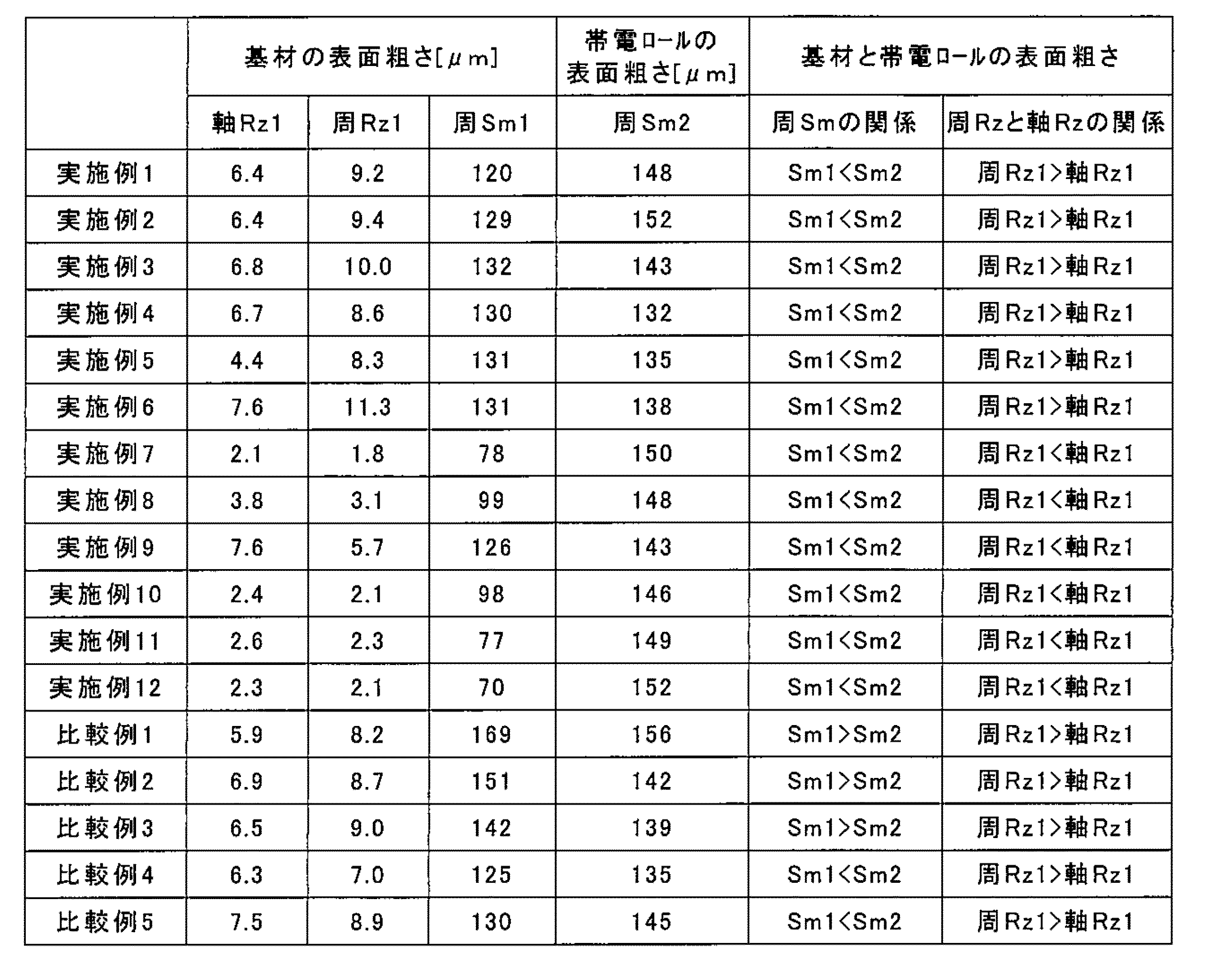
<画像均一性(濃度ムラ)評価>
次に、プリンタ実機を用いて帯電ロールの画像評価試験を行った。具体的には、得られた帯電ロールをプリンタ実機(A3サイズ カラーMFP 25枚/分 機)に適用し、下記印刷条件で印刷した画像について、色彩色差計(コニカミノルタ製CR-400)を用いて画像均一性(濃度ムラ)を評価し、その結果を下記表3に示した。画像の濃度ムラの評価は、画像の四隅及び中央2箇所の合計6箇所についてL*を測定し、これらのバラツキσを算出した。なお、評価基準は、以下に示した通りである。 <Evaluation of image uniformity (density unevenness)>
Next, an image evaluation test of the charging roll was performed using the actual printer. Specifically, the obtained charging roll was applied to an actual printer (A3 size color MFP 25 sheets / machine), and a color difference meter (CR-400 manufactured by Konica Minolta) was used for an image printed under the following printing conditions. The image uniformity (density unevenness) was evaluated, and the results are shown in Table 3 below. For the evaluation of density unevenness of the image, L * was measured at a total of six places including the four corners and the center of the image, and the variation σ was calculated. The evaluation criteria are as shown below.
[印刷条件]
印加電圧:DC=-1000V
速度 :154mm/sec
印刷環境:10℃×20% [Printing conditions]
Applied voltage: DC = -1000V
Speed: 154mm / sec
Printing environment: 10 ° C x 20%
印加電圧:DC=-1000V
速度 :154mm/sec
印刷環境:10℃×20% [Printing conditions]
Applied voltage: DC = -1000V
Speed: 154mm / sec
Printing environment: 10 ° C x 20%
[評価基準]
○:画像の濃度ムラなし(L*6箇所バラツキσ0.06以下)
△:画像の濃度ムラあり(L*6箇所バラツキσ0.06超過0.32以下)
×:画像の濃度ムラあり(L*6箇所バラツキσ0.32超過) [Evaluation criteria]
○: Image density unevenness (L * 6 variation σ0.06 or less)
Δ: Density of image unevenness (L * 6 variation σ0.06 over 0.32 or less)
×: Image density unevenness (L * 6 variation σ0.32 exceeded)

(実施例2,3)
実施例2,3は、コーティング液の表面付与材の添加量を変更した以外は実施例1と同様にして帯電ロールを作製し(表1参照)、基材及び帯電ロールの表面粗さを測定し(表2参照)、帯電ロールを適用したプリンタ実機の画像均一性(濃度ムラ)を評価した(表3参照)。 (Examples 2 and 3)
In Examples 2 and 3, a charging roll was prepared in the same manner as in Example 1 except that the amount of the surface-imparting material added to the coating solution was changed (see Table 1), and the surface roughness of the base material and the charging roll was measured. (See Table 2), and the image uniformity (density unevenness) of the actual printer to which the charging roll was applied was evaluated (see Table 3).
(実施例4~6)
実施例4~6は、コーティング液の希釈溶媒を変更した以外は実施例3と同様にして帯電ロールを作製し(表1参照)、基材及び帯電ロールの表面粗さを測定し(表2参照)、帯電ロールを適用したプリンタ実機の画像均一性(濃度ムラ)を評価した(表3参照)。 (Examples 4 to 6)
In Examples 4 to 6, a charging roll was prepared in the same manner as in Example 3 except that the dilution solvent of the coating solution was changed (see Table 1), and the surface roughness of the substrate and the charging roll was measured (Table 2). The image uniformity (density unevenness) of the actual printer to which the charging roll was applied was evaluated (see Table 3).
(実施例7)
実施例7は、基材の周Rz1と軸Rz1の関係を変化させた以外は実施例1と同様にして帯電ロールを作製し(表1参照)、基材及び帯電ロールの表面粗さを測定し(表2参照)、帯電ロールを適用したプリンタ実機の画像均一性(濃度ムラ)を評価した(表3参照)。実施例7では、基材表面を研磨した後に耐水研磨ペーパーを用いて湿式研磨機で追加研磨を行って、基材の周Rz1と軸Rz1の関係を変化させた。 (Example 7)
In Example 7, a charging roll was prepared in the same manner as in Example 1 except that the relationship between the circumference Rz1 and the axis Rz1 of the base material was changed (see Table 1), and the surface roughness of the base material and the charging roll was measured. (See Table 2), and the image uniformity (density unevenness) of the actual printer to which the charging roll was applied was evaluated (see Table 3). In Example 7, after polishing the substrate surface, additional polishing was performed with a wet polishing machine using water-resistant polishing paper to change the relationship between the circumference Rz1 and the axis Rz1 of the substrate.
(実施例8,9)
実施例8,9は、コーティング液の表面付与材の添加量を変更した以外は実施例7と同様にして帯電ロールを作製し(表1参照)、基材及び帯電ロールの表面粗さを測定し(表2参照)、帯電ロールを適用したプリンタ実機の画像均一性(濃度ムラ)を評価した(表3参照)。 (Examples 8 and 9)
In Examples 8 and 9, a charging roll was prepared in the same manner as in Example 7 except that the amount of the surface-imparting material added to the coating liquid was changed (see Table 1), and the surface roughness of the substrate and the charging roll was measured. (See Table 2), and the image uniformity (density unevenness) of the actual printer to which the charging roll was applied was evaluated (see Table 3).
(実施例10~12)
実施例10~12は、コーティング液の希釈溶媒を変更した以外は実施例8と同様にして帯電ロールを作製し(表1参照)、基材及び帯電ロールの表面粗さを測定し(表2参照)、帯電ロールを適用したプリンタ実機の画像均一性(濃度ムラ)を評価した(表3参照)。 (Examples 10 to 12)
In Examples 10 to 12, a charging roll was prepared in the same manner as in Example 8 except that the dilution solvent of the coating solution was changed (see Table 1), and the surface roughness of the substrate and the charging roll was measured (Table 2). The image uniformity (density unevenness) of the actual printer to which the charging roll was applied was evaluated (see Table 3).
(比較例1)
比較例1は、基材の周Sm1と帯電ロールの周Sm2の関係を変化させた以外は実施例1と同様にして帯電ロールを作製し(表1参照)、基材及び帯電ロールの表面粗さを測定し(表2参照)、帯電ロールを適用したプリンタ実機の画像均一性(濃度ムラ)を評価した(表3参照)。比較例1では、基材表面を研磨する際に研磨機の砥石回転数を3000rpm、2000rpm、1000rpmのように順次下げていくことにより、基材の周Sm1を135μmより大きくしてコーティング層を形成した。 (Comparative Example 1)
In Comparative Example 1, a charging roll was prepared in the same manner as in Example 1 except that the relationship between the circumference Sm1 of the base material and the circumference Sm2 of the charging roll was changed (see Table 1). The thickness was measured (see Table 2), and the image uniformity (density unevenness) of the actual printer to which the charging roll was applied was evaluated (see Table 3). In Comparative Example 1, when the surface of the base material is polished, the grinding wheel rotational speed of the polishing machine is sequentially decreased to 3000 rpm, 2000 rpm, and 1000 rpm, thereby forming the coating layer by making the circumference Sm1 of the base material larger than 135 μm. did.
(比較例2,3)
比較例2,3は、コーティング液の表面付与材の添加量を変更した以外は比較例1と同様にして帯電ロールを作製し(表1参照)、基材及び帯電ロールの表面粗さを測定し(表2参照)、帯電ロールを適用したプリンタ実機の画像均一性(濃度ムラ)を評価した(表3参照)。 (Comparative Examples 2 and 3)
In Comparative Examples 2 and 3, a charging roll was prepared in the same manner as in Comparative Example 1 except that the amount of the surface-imparting material added to the coating liquid was changed (see Table 1), and the surface roughness of the substrate and the charging roll was measured. (See Table 2), and the image uniformity (density unevenness) of the actual printer to which the charging roll was applied was evaluated (see Table 3).
(比較例4,5)
比較例4,5は、コーティング液の表面付与材の添加量を変更した以外は実施例1と同様にして帯電ロールを作製し(表1参照)、基材及び帯電ロールの表面粗さを測定し(表2参照)、帯電ロールを適用したプリンタ実機の画像均一性(濃度ムラ)を評価した(表3参照)。 (Comparative Examples 4 and 5)
In Comparative Examples 4 and 5, a charging roll was prepared in the same manner as in Example 1 except that the amount of the surface-imparting material added to the coating liquid was changed (see Table 1), and the surface roughness of the substrate and the charging roll was measured. (See Table 2), and the image uniformity (density unevenness) of the actual printer to which the charging roll was applied was evaluated (see Table 3).
(結果のまとめ)
実施例1~3の帯電ロールは、研磨機の砥石回転数を1000rpm、2000rpm、3000rpmのように順次上げて研磨したことにより、基材の周Sm1が135μm以下となり、周Rz1が15μm以下及び軸Rz1が10μm以下であり、また、周Rz1と軸Rz1の差が0.1μm以上であった。このような基材を用い、更に、表面付与材の添加量を4質量部以上、45質量部以下にしたコーティング液を用いてコーティング層を形成したことにより、周Sm1が周Sm2よりも小さい表面粗さの帯電ロールがそれぞれ得られた。その結果、これらの帯電ロールの画像評価試験では、濃度ムラがなく均一な画像が得られた。 (Summary of results)
The charging rolls of Examples 1 to 3 were polished by sequentially increasing the grindstone rotation speed of the polishing machine to 1000 rpm, 2000 rpm, and 3000 rpm, so that the circumference Sm1 of the base material was 135 μm or less, the circumference Rz1 was 15 μm or less, and the shaft Rz1 was 10 μm or less, and the difference between the circumference Rz1 and the axis Rz1 was 0.1 μm or more. By using such a base material and further forming a coating layer using a coating liquid in which the addition amount of the surface-imparting material is 4 parts by mass or more and 45 parts by mass or less, the surface having a circumference Sm1 smaller than the circumference Sm2 Rough charging rolls were obtained respectively. As a result, in the image evaluation test of these charging rolls, uniform images with no density unevenness were obtained.
また、実施例4~6のように希釈溶媒が水以外であっても、実施例7~9のように周Rz1が軸Rz1よりも小さく且つこれらの差が-0.1μm以下であっても、実施例10~12のように希釈溶媒が水以外であり、周Rz1が軸Rz1よりも小さく且つこれらの差が-0.1μm以下であっても、実施例1~3の画像評価試験の結果と差異が無く、これらの条件においては、画像の濃度ムラを生じさせないことがわかった。
Even if the diluent solvent is other than water as in Examples 4 to 6, even if the circumference Rz1 is smaller than the axis Rz1 and the difference between these is −0.1 μm or less as in Examples 7 to 9. Even if the diluent solvent is other than water as in Examples 10 to 12, the circumference Rz1 is smaller than the axis Rz1 and the difference between these is −0.1 μm or less, the image evaluation tests of Examples 1 to 3 There was no difference from the results, and it was found that there was no uneven density in the image under these conditions.
一方、比較例1~3では、基材の軸Rz1が10μm以下及び周Rz1が15μm以下であっても、周Sm1が135μmを超えていた。このような好ましくない表面粗さの基材を用いたために、その好ましくない表面状態を維持してコーティング層が形成され、周Sm1が周Sm2よりも大きくなった。その結果、これらの帯電ロールの画像評価試験では、画像の濃度ムラが観察された。また、比較例4では、コーティング液の表面付与材の添加量が4質量部未満であり、比較例5では、この添加量が45質量部を超えていたために、式(1)を満たした基材を用いても、その表面粗さを維持することができなかった。その結果、得られた帯電ロールの画像評価試験では、画像の濃度ムラが観察された。
On the other hand, in Comparative Examples 1 to 3, even when the base axis Rz1 was 10 μm or less and the circumference Rz1 was 15 μm or less, the circumference Sm1 exceeded 135 μm. Since the substrate having such an unfavorable surface roughness was used, the coating layer was formed while maintaining the unfavorable surface state, and the circumference Sm1 was larger than the circumference Sm2. As a result, in the image evaluation test of these charging rolls, image density unevenness was observed. In Comparative Example 4, the amount of the surface-imparting material added to the coating liquid was less than 4 parts by mass. In Comparative Example 5, the amount of addition exceeded 45 parts by mass, so that the group satisfying the formula (1) was satisfied. Even if the material was used, the surface roughness could not be maintained. As a result, in the image evaluation test of the obtained charging roll, density unevenness of the image was observed.
本発明にかかる導電性ロールは、特に電子写真方式の複写機やプリンタ等の画像形成装置の帯電ロールの他、現像ロール、帯電ロール、転写ロール、トナー供給ロール等に用いて好適である。
The conductive roll according to the present invention is particularly suitable for use as a developing roll, a charging roll, a transfer roll, a toner supply roll, etc. in addition to a charging roll of an image forming apparatus such as an electrophotographic copying machine or printer.
10 帯電ロール
11 芯体
12 弾性層
13 基材
14 コーティング層 DESCRIPTION OFSYMBOLS 10 Charging roll 11 Core 12 Elastic layer 13 Base material 14 Coating layer
11 芯体
12 弾性層
13 基材
14 コーティング層 DESCRIPTION OF
Claims (4)
- 芯体の外周に少なくとも1層の導電性ゴム体を主体とする弾性層と、
前記弾性層の外周にコーティング層とを有し、
前記弾性層の周方向の凹凸の平均間隔Smを周Sm1、前記コーティング層の周方向の凹凸の平均間隔Smを周Sm2としたとき、下記式(1)及び式(2)を満たすことを特徴とする導電性ロール。
周Sm1≦135μm ・・・ (1)
周Sm1<周Sm2 ・・・ (2) An elastic layer mainly composed of at least one conductive rubber body on the outer periphery of the core;
A coating layer on the outer periphery of the elastic layer;
When the average interval Sm of the irregularities in the circumferential direction of the elastic layer is the circumference Sm1, and the average interval Sm of the irregularities in the circumferential direction of the coating layer is the circumference Sm2, the following expressions (1) and (2) are satisfied. A conductive roll.
Circumference Sm1 ≦ 135 μm (1)
Circumference Sm1 <lap Sm2 (2) - 前記弾性層の周方向の十点平均粗さRzを周Rz1としたとき、下記式(3)を満たすことを特徴とする請求項1に記載の導電性ロール。
周Rz1≦15μm ・・・ (3) 2. The conductive roll according to claim 1, wherein when the ten-point average roughness Rz in the circumferential direction of the elastic layer is defined as a circumference Rz1, the following formula (3) is satisfied.
Circumference Rz1 ≦ 15 μm (3) - 前記弾性層の軸方向の十点平均粗さRzを軸Rz1としたとき、下記式(4)及び式(5)を満たすことを特徴とする請求項1又は請求項2に記載の導電性ロール。
|軸Rz1-周Rz1|≧0.1μm ・・・ (4)
軸Rz1≦10μm ・・・ (5) The conductive roll according to claim 1 or 2, wherein when the ten-point average roughness Rz in the axial direction of the elastic layer is an axis Rz1, the following formula (4) and formula (5) are satisfied. .
| Axis Rz1-Round Rz1 | ≧ 0.1 μm (4)
Axis Rz1 ≦ 10 μm (5) - 前記コーティング層がベース材、導電材及び表面粗さ付与材を含み、これらの全量が35質量部~175質量部であるとき、前記表面粗さ付与材の添加量は、4質量部~45質量部であることを特徴とする請求項1~請求項3の何れか1項に記載の導電性ロール。 When the coating layer includes a base material, a conductive material, and a surface roughness imparting material, and the total amount thereof is 35 parts by mass to 175 parts by mass, the amount of the surface roughness imparting material added is 4 parts by mass to 45 parts by mass. The conductive roll according to any one of claims 1 to 3, wherein the conductive roll is a part.
Priority Applications (5)
| Application Number | Priority Date | Filing Date | Title |
|---|---|---|---|
| CN201780010880.2A CN108604074B (en) | 2016-08-04 | 2017-08-01 | Conductive roller |
| EP17836973.2A EP3379337A4 (en) | 2016-08-04 | 2017-08-01 | Conductive roll |
| JP2017562790A JP6303095B1 (en) | 2016-08-04 | 2017-08-01 | Conductive roll |
| US16/069,432 US10268133B2 (en) | 2016-08-04 | 2017-08-01 | Conductive roll |
| MYPI2018001141A MY188632A (en) | 2016-08-04 | 2017-08-01 | Conductive roller |
Applications Claiming Priority (2)
| Application Number | Priority Date | Filing Date | Title |
|---|---|---|---|
| JP2016-154012 | 2016-08-04 | ||
| JP2016154012 | 2016-08-04 |
Publications (1)
| Publication Number | Publication Date |
|---|---|
| WO2018025870A1 true WO2018025870A1 (en) | 2018-02-08 |
Family
ID=61073991
Family Applications (1)
| Application Number | Title | Priority Date | Filing Date |
|---|---|---|---|
| PCT/JP2017/027917 WO2018025870A1 (en) | 2016-08-04 | 2017-08-01 | Conductive roll |
Country Status (6)
| Country | Link |
|---|---|
| US (1) | US10268133B2 (en) |
| EP (1) | EP3379337A4 (en) |
| JP (1) | JP6303095B1 (en) |
| CN (1) | CN108604074B (en) |
| MY (1) | MY188632A (en) |
| WO (1) | WO2018025870A1 (en) |
Cited By (1)
| Publication number | Priority date | Publication date | Assignee | Title |
|---|---|---|---|---|
| JP2019192777A (en) * | 2018-04-25 | 2019-10-31 | 株式会社ディスコ | Chuck table and manufacturing method of the chuck table |
Families Citing this family (3)
| Publication number | Priority date | Publication date | Assignee | Title |
|---|---|---|---|---|
| EP3848760B1 (en) * | 2018-09-05 | 2022-07-13 | NOK Corporation | Conductive roll |
| US10824087B2 (en) * | 2019-03-20 | 2020-11-03 | Fuji Xerox Co., Ltd. | Charging member, charging device, process cartridge, and image forming apparatus |
| US11714364B2 (en) * | 2019-08-29 | 2023-08-01 | Nok Corporation | Charging roll |
Citations (7)
| Publication number | Priority date | Publication date | Assignee | Title |
|---|---|---|---|---|
| JPH0749605A (en) * | 1993-05-31 | 1995-02-21 | Ricoh Co Ltd | Electrostatically charging roller |
| JP2004306519A (en) * | 2003-04-09 | 2004-11-04 | Canon Inc | Conductive member |
| JP2006145956A (en) * | 2004-11-22 | 2006-06-08 | Canon Inc | Developing roller, process cartridge, and image forming apparatus |
| JP2009080207A (en) * | 2007-09-25 | 2009-04-16 | Oki Data Corp | Developing device and image forming apparatus |
| JP2011095725A (en) * | 2009-09-30 | 2011-05-12 | Synztec Co Ltd | Charging roll |
| JP2011232433A (en) * | 2010-04-26 | 2011-11-17 | Oki Data Corp | Charging component, image formation unit, and image forming apparatus |
| JP2015052680A (en) * | 2013-09-06 | 2015-03-19 | コニカミノルタ株式会社 | Endless tubular belt |
Family Cites Families (10)
| Publication number | Priority date | Publication date | Assignee | Title |
|---|---|---|---|---|
| JP4193193B2 (en) | 2001-10-16 | 2008-12-10 | シンジーテック株式会社 | Conductive roll |
| US6684043B1 (en) * | 2002-08-27 | 2004-01-27 | Xerox Corporation | Long life charging apparatus |
| JP2005091414A (en) | 2003-09-12 | 2005-04-07 | Ricoh Co Ltd | Electrifying roller, method for manufacturing electrifying roller, process cartridge, and image forming apparatus |
| WO2010050615A1 (en) * | 2008-10-31 | 2010-05-06 | キヤノン株式会社 | Charging member, process cartridge, and electrophotographic apparatus |
| JP5504713B2 (en) * | 2009-07-02 | 2014-05-28 | 富士ゼロックス株式会社 | Conductive roll, charging device, process cartridge, and image forming apparatus |
| CN102033459B (en) | 2009-09-30 | 2014-08-06 | 新智德株式会社 | Charged roller |
| JP5663296B2 (en) | 2010-06-04 | 2015-02-04 | 京セラドキュメントソリューションズ株式会社 | Image forming apparatus |
| JP6128424B2 (en) * | 2012-10-25 | 2017-05-17 | 株式会社リコー | Image forming apparatus and process cartridge |
| CN105339848B (en) * | 2013-06-27 | 2018-07-20 | 佳能株式会社 | Image forming apparatus and handle box |
| JP6067632B2 (en) | 2013-11-21 | 2017-01-25 | 三星電子株式会社Samsung Electronics Co.,Ltd. | Charging member |
-
2017
- 2017-08-01 WO PCT/JP2017/027917 patent/WO2018025870A1/en active Application Filing
- 2017-08-01 JP JP2017562790A patent/JP6303095B1/en active Active
- 2017-08-01 MY MYPI2018001141A patent/MY188632A/en unknown
- 2017-08-01 CN CN201780010880.2A patent/CN108604074B/en active Active
- 2017-08-01 EP EP17836973.2A patent/EP3379337A4/en active Pending
- 2017-08-01 US US16/069,432 patent/US10268133B2/en active Active
Patent Citations (7)
| Publication number | Priority date | Publication date | Assignee | Title |
|---|---|---|---|---|
| JPH0749605A (en) * | 1993-05-31 | 1995-02-21 | Ricoh Co Ltd | Electrostatically charging roller |
| JP2004306519A (en) * | 2003-04-09 | 2004-11-04 | Canon Inc | Conductive member |
| JP2006145956A (en) * | 2004-11-22 | 2006-06-08 | Canon Inc | Developing roller, process cartridge, and image forming apparatus |
| JP2009080207A (en) * | 2007-09-25 | 2009-04-16 | Oki Data Corp | Developing device and image forming apparatus |
| JP2011095725A (en) * | 2009-09-30 | 2011-05-12 | Synztec Co Ltd | Charging roll |
| JP2011232433A (en) * | 2010-04-26 | 2011-11-17 | Oki Data Corp | Charging component, image formation unit, and image forming apparatus |
| JP2015052680A (en) * | 2013-09-06 | 2015-03-19 | コニカミノルタ株式会社 | Endless tubular belt |
Non-Patent Citations (1)
| Title |
|---|
| See also references of EP3379337A4 * |
Cited By (1)
| Publication number | Priority date | Publication date | Assignee | Title |
|---|---|---|---|---|
| JP2019192777A (en) * | 2018-04-25 | 2019-10-31 | 株式会社ディスコ | Chuck table and manufacturing method of the chuck table |
Also Published As
| Publication number | Publication date |
|---|---|
| JP6303095B1 (en) | 2018-04-04 |
| US10268133B2 (en) | 2019-04-23 |
| EP3379337A4 (en) | 2019-11-13 |
| JPWO2018025870A1 (en) | 2018-08-02 |
| CN108604074A (en) | 2018-09-28 |
| US20190025727A1 (en) | 2019-01-24 |
| EP3379337A1 (en) | 2018-09-26 |
| MY188632A (en) | 2021-12-22 |
| CN108604074B (en) | 2020-07-24 |
Similar Documents
| Publication | Publication Date | Title |
|---|---|---|
| JP6303095B1 (en) | Conductive roll | |
| JP7394928B2 (en) | charging roll | |
| JP7342209B2 (en) | charging roll | |
| JP2022126823A (en) | charging roll | |
| JP2019191519A (en) | Conductive roller | |
| JP7337176B2 (en) | charging roll | |
| WO2019044829A1 (en) | Electroconductive roll | |
| JP7337177B2 (en) | charging roll | |
| WO2020175434A1 (en) | Charging roller | |
| JPWO2020175431A1 (en) | Charging roll | |
| WO2020175436A1 (en) | Charging roller | |
| WO2020175437A1 (en) | Charging roller | |
| WO2020175432A1 (en) | Charging roll | |
| WO2020175433A1 (en) | Charging roll | |
| CN113242939B (en) | Charging roller | |
| JP7342136B2 (en) | charging roll | |
| CN114270275B (en) | Charging roller |
Legal Events
| Date | Code | Title | Description |
|---|---|---|---|
| ENP | Entry into the national phase |
Ref document number: 2017562790 Country of ref document: JP Kind code of ref document: A |
|
| WWE | Wipo information: entry into national phase |
Ref document number: 2017836973 Country of ref document: EP |
|
| NENP | Non-entry into the national phase |
Ref country code: DE |