WO2018021749A1 - Led 조명장치 및 이의 led 구동회로 - Google Patents
Led 조명장치 및 이의 led 구동회로 Download PDFInfo
- Publication number
- WO2018021749A1 WO2018021749A1 PCT/KR2017/007697 KR2017007697W WO2018021749A1 WO 2018021749 A1 WO2018021749 A1 WO 2018021749A1 KR 2017007697 W KR2017007697 W KR 2017007697W WO 2018021749 A1 WO2018021749 A1 WO 2018021749A1
- Authority
- WO
- WIPO (PCT)
- Prior art keywords
- led
- voltage
- node
- driving
- switch unit
- Prior art date
- Legal status (The legal status is an assumption and is not a legal conclusion. Google has not performed a legal analysis and makes no representation as to the accuracy of the status listed.)
- Ceased
Links
Images




Classifications
-
- H—ELECTRICITY
- H05—ELECTRIC TECHNIQUES NOT OTHERWISE PROVIDED FOR
- H05B—ELECTRIC HEATING; ELECTRIC LIGHT SOURCES NOT OTHERWISE PROVIDED FOR; CIRCUIT ARRANGEMENTS FOR ELECTRIC LIGHT SOURCES, IN GENERAL
- H05B45/00—Circuit arrangements for operating light-emitting diodes [LED]
Definitions
- Embodiment of the present invention relates to an LED driving device of the AC drive method and the LED driving circuit included therein.
- a circuit in order to drive an LED lighting device using an alternating voltage, a circuit is configured to convert the alternating voltage into a rectified voltage and adjust the number of LED light emitting elements that emit light as the magnitude of the rectified voltage changes.
- the light emitting time is determined to be long, while some of the light emitting diodes are limited to light only when the size of the rectified voltage is above a certain level. Since the light emitting time is different for each of the LED light emitting elements constituting the lighting device. As a result, some of the LED light emitting elements may first deteriorate, resulting in a poor lighting condition of the lighting device, or in some cases, the operation of the lighting device may be impossible.
- the voltage level of the commercial AC power supply currently supplied by each country is different.
- AC power of 220V (rms) is supplied in Korea, but AC power of 120V (rms) or AC power of 277V (rms) may be supplied in other countries.
- separate circuits capable of performing a universal voltage function must be added to the LED lighting device.
- An embodiment of the present invention is to provide a LED lighting device and a driving circuit thereof that can implement a universal voltage function without additional circuitry by controlling the connection relationship between the LED groups to correspond to the commercial AC power input.
- the LED lighting apparatus a rectifier for rectifying the AC voltage input from the external power source to generate a drive voltage;
- An LED light emitting unit including a first LED group connected to a first node connected to an output terminal of the rectifier and a plurality of LED groups connected in series with a phase first LED group;
- a switch unit controller receiving the driving voltage to generate a voltage value associated with the external power source, and outputting a control signal by comparing the generated voltage value with a preset reference voltage value;
- a switch unit connected between the first node and a second node located between the LED groups, the switch unit being turned on / off by the control signal to change a connection relationship between the LED groups;
- a driving current controller connected to the respective LED groups and configured to control the constant current of the driving current flowing through each of the LED groups.
- the external power source is one of commercial AC power sources having different effective voltage values.
- the second node is a node between a cathode end of the first LED group and an anode end of the second LED group adjacent thereto, and a diode is further provided between the cathode end of the first LED group and the second node.
- the switch unit controller may further include a resistor and a capacitor connected in series between the first node and ground; The voltage of the capacitor is applied to the negative input terminal, the reference voltage is applied to the positive input terminal, and comprises a comparator for comparing the output signal.
- the voltage of the capacitor has a different level of voltage value for each commercial AC power corresponding to the input commercial AC power, the reference voltage is set to any effective voltage value between the commercial AC power do.
- the switch unit may further include: a control transistor controlled by a control signal output from the switch control unit; And a switching transistor connected between the first node and the second node and having a gate electrode connected to the first electrode of the control transistor.
- control transistor is connected between the gate electrode and the ground of the switch transistor, the control signal is applied to the gate electrode, in parallel with the resistance and the resistance connected between the drain electrode and the gate electrode of the switching transistor.
- a zener diode to be connected is further included.
- the LED driving circuit receives a driving voltage generated by the external power is rectified to generate a voltage value associated with the external power, and compares the generated voltage value with a predetermined reference voltage value
- a switch unit controller for outputting a control signal
- a switch unit connected between a first node to which the driving voltage is applied and a second node between the LED groups, and a turn-on / off is controlled by the control signal to change a connection relationship between the LED groups;
- a driving current controller connected to the respective LED groups and configured to control the constant current of the driving current flowing through each of the LED groups.
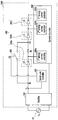
- FIG. 1 is a block diagram of an LED lighting apparatus according to an embodiment of the present invention.
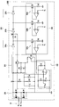
- FIG. 2 is a schematic circuit diagram of an LED lighting apparatus according to an embodiment of the present invention.
- FIG. 3 is a schematic circuit diagram illustrating the operation of the drive current controller shown in FIG. 1;
- FIG. 4 is a schematic circuit diagram illustrating the operation of the switch unit controller shown in FIG. 1;
- FIG. 5 is a schematic circuit diagram explaining the operation of the switch unit shown in FIG. 1;
- FIG. 5 is a schematic circuit diagram explaining the operation of the switch unit shown in FIG. 1;
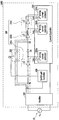
- Figure 6a is a block diagram illustrating the operation when the LED lighting apparatus according to an embodiment of the present invention is connected to a 120V (rms) AC power supply.
- 6B is a waveform diagram showing the relationship between the rectified voltage and the LED driving current when the LED lighting apparatus according to the embodiment of the present invention is connected to a 120V (rms) AC power source.
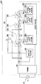
- Figure 7a is a block diagram illustrating the operation when the LED lighting apparatus according to an embodiment of the present invention is connected to a 220V (rms) AC power source.
- FIG. 7B is a waveform diagram showing the relationship between the rectified voltage and the LED driving current when the LED lighting apparatus according to the embodiment of the present invention is connected to a 220V (rms) AC power source.
- first, second, etc. may be used to describe various elements, elements, regions, layers, and / or sections, but such elements, elements, regions, layers, and / or the like. Or sections are not limited to these terms. These terms are used to distinguish one element, element, region, layer, and / or section from another element, element, region, layer, and / or section. Thus, the first element, element, region, layer, and / or section in one embodiment may be referred to as the second element, element, region, layer, and / or section in another embodiment.
- FIG. 1 is a block diagram of an LED lighting apparatus according to an embodiment of the present invention
- Figure 2 is a circuit diagram of an LED lighting apparatus according to an embodiment of the present invention.
- the LED lighting apparatus 1000 is a rectifier 100, LED light emitting unit 200, switch unit 300, switch unit controller 400, current controller 500 may be included.
- the LED light emitting unit 200 may be composed of a plurality of LED groups 200a, 200b, and 200c.
- the plurality of LED groups 200a, 200b, and 200c included in the LED light emitting unit 200 may be controlled to be connected to each other according to the operation of the switch unit 300.
- the LED groups 200a, 200b, and 200c when the LED groups 200a, 200b, and 200c are connected in series, the LED groups connected in series may be sequentially driven according to the operation of the current controller 500.
- FIG 1 illustrates an LED light emitting unit 200 including three LED groups from the first LED group 200a to the third LED group 200c, but included in the LED light emitting unit 200 as necessary. It will be apparent to those skilled in the art that the number of LED groups to be varied may vary.
- the LED light emitting unit 200 will be described based on the embodiment consisting of three LED groups, but the present invention is not limited thereto.
- the LED light emitting unit 200 may be composed of n LED groups from the first LED group 200a to the nth LED group (not shown) (n is a positive integer of 2 or more).
- the first LED group 200a to the third LED group 200c may have the same forward voltage level or may have different forward voltage levels.
- the first LED group 200a to the third LED group 200c each includes a different number of LED elements, or the first LED group 200a to the third LED group 200c are each different.
- the first LED group 200a to the third LED group 200c may have different forward voltage levels.
- the first LED group 200a to the third LED group 200c will be described based on the embodiment configured to have the same forward voltage level.
- the first forward voltage level Vf1 is a threshold voltage level capable of driving the first LED group 200a
- the second forward voltage level Vf2 is the first LED group 200a and the first connected in series.
- the threshold voltage level capable of driving the two LED groups 200b ie, the voltage level obtained by adding the forward voltage level of the first LED group and the forward voltage level of the second LED group
- the third forward voltage level Vf3 is It may be a threshold voltage level capable of driving the first to third LED groups 200a, 200b, and 200c connected in series.
- the rectifier 100 is configured to rectify the AC voltage (V AC ) input from the external power source 10 to generate and output a rectified voltage, the rectified voltage is a driving voltage applied to the LED light emitting unit 400 ( V in ).
- the rectifier 100 may employ a rectifier circuit well known in the art, such as a diode bridge circuit including diodes d1, d2, d3, and d4.
- the external power source 10 may be a commercial AC power source, and the commercial AC power source may be a voltage of 120 V (rms), 220 V (rms), or 277 V (rms).
- the switch unit controller 400 receives a driving voltage (V in ) and generates a voltage value associated with a commercial AC power source 10 connected to the LED lighting device 1000, and generates the preset reference voltage value. Compared to the control signal (CS) for controlling the operation of the switch unit 300 is output. However, the switch unit controller 400 may directly receive an AC voltage V AC input from an external power source 10 in addition to the driving voltage V in .
- the switch unit controller 400 includes a first resistor R1 and a capacitor C connected in series between the first node N1 connected to the output terminal of the rectifier 100 and a ground. And a second resistor R2 and a zener diode dz respectively connected in parallel to the capacitor C.
- the apparatus may further include a comparator configured to receive a voltage applied to the capacitor C through a negative input terminal ( ⁇ ). In this case, a reference voltage is applied to the positive input terminal (+) of the comparator, and the reference voltage may be generated through the regulator (G).
- the regulator G may be implemented as a shunt regulator, and may be connected in parallel with the DC power supply V DC through a resistor r1 connected in series.
- a pull-up resistor r2 is connected to an output terminal of the comparator, and the DC power supply V DC illustrated in FIG. 2 provides an operating voltage for operating the comparator and the regulator G. can do.
- the first resistor R1 and the second resistor R2 may divide the detected input voltage, and the zener diode dz may serve to protect the comparator from the input overvoltage.
- the switch unit 300 performs a turn on / off operation by the control signal CS, and as illustrated, the switch unit 300 is disposed between the first node N1 and the second node N2. Connected.
- the first node N1 may be a node connected to the output terminal of the rectifier 100
- the second node N1 may be a node between the LED groups 200a, 200b, and 200c.
- the switch unit 300 includes resistors RZ connected between different types of transistors QW and QS and between the first node N1 and the gate electrode of the transistor QW, respectively.
- Zener diode (DZ) may be included.
- the driving voltage V in output from the rectifier 100 is connected to the first LED group 200a to the third LED connected in series. It is sequentially applied to the group 200c and sequentially driven according to the voltage level of the driving voltage V in .
- the first LED group 200a is driven in a section (first operating period) in which the voltage level of the driving voltage V in is greater than or equal to the first forward voltage level Vf1 and less than the second forward voltage level Vf2.
- the first LED group 200a and the second LED group in the second operation period) when the voltage level of the driving voltage V in is greater than or equal to the second forward voltage level 2Vf and less than the third forward voltage level Vf3.
- 200b is driven and the first LED group 200a, the second LED group 200b and the second LED group 200b in a section (third operating period) where the voltage level of the driving voltage V in is greater than or equal to the third forward voltage level Vf3. All of the third LED groups 200c are driven.
- the driving voltage V in is not only the first LED group 200a connected to the first node N1 but also the second LED group connected to the second node N2 ( 200b) is also applied directly.
- the second node N2 may be a node between the cathode end of the first LED group 200a and the anode end of the second LED group 200b.
- the driving voltage V in is applied to the second node N2
- the cathode terminal and the second node N2 of the first LED group 200a are illustrated to prevent generation of reverse current paths.
- the diode D1 may be provided between the electrodes.
- the LED light emitting unit 200 is divided into two sets, respectively for each LED group corresponding to each set.
- the driving is sequentially performed according to the voltage level of the applied driving voltage V in .
- the term 'set' refers to at least one LED group connected in series with each other to form one unit.
- the second LED group 200b and the third LED group 200c become one set, they are sequentially driven in the set. Namely, in the voltage level of the driving voltage (V in), a first forward voltage level (Vf1) than the second forward voltage level (Vf2) lower than interval (the first operation period) is driven, only the second LED group (200b), The second LED group 200b and the third LED group (in the second operation period) when the voltage level of the driving voltage V in is greater than or equal to the second forward voltage level Vf2 and less than the third forward voltage level Vf3. 200c) may be driven.
- first LED group 200a separated into a separate set may be driven during the first operation period and the second operation period.
- the current controller 500 includes a plurality of driving current controllers 500a, 500b, and 500c. 1 includes first to third drive current controllers 500a, 500b and 500c, which are connected to the cathode ends of the first LED group 200a to the third LED group 200c, respectively. .
- a target voltage Vt may be applied to each of the driving current controllers 500a, 500b, and 500c, and may be applied to the first to third driving current controllers 500a, 500b, and 500c according to the target voltage Vt.
- the amount of current of the connected first to third LED groups 200a, 200b, and 200c is determined, respectively.
- the first to third driving current controllers 500a, 500b, and 500c perform an operation of controlling the first to third driving currents flowing through the first to third LED groups 200a, 200b, and 200c with a constant current. can do.
- the target voltage Vt may be set differently for each of the driving current controllers 500a, 500b, and 500c, and in this case, the first to third driving currents may be constant current controlled according to a preset value.
- Each of the driving current controllers 500a, 500b, and 500c may include a transistor Qd, a sense resistor Rd, and a linear amplifier as shown in FIG. 2.
- the LED lighting apparatus 1000 detects a voltage level corresponding to the input commercial AC power supply 10 and according to the detected voltage level, the LED light emitting device groups 200a, 200b, and 200c. By performing the operation of controlling the connection between the two, it is possible to implement a universal voltage (universal voltage) function without additional circuitry.
- the switch unit controller 400, the switch unit 300, and the current controller 500 may be integrated into one IC, which receives the driving voltage V in to receive the LED light emitting unit 200. It can serve as a driving LED driving circuit.
- FIG. 3 is a schematic circuit diagram illustrating the operation of the driving current controller shown in FIG. 1.
- 3 illustrates the first driving current controller 500a as an example, the second and third driving current controllers may be configured in the same manner.
- the driving current controller 500a includes a linear amplifier 520, a transistor Qd, and a detection resistor Rd.
- the voltage detected by the detection resistor Rd may be applied to the negative input terminal of the linear amplifier 520, and the target voltage Vt described above may be applied to the positive input terminal.
- the output of the linear amplifier 520 may be input to the gate electrode of the transistor Qd.
- the transistor Qd may be variously implemented as a switching element for constant current control.
- the transistor Qd is connected between the cathode terminal of each of the LED groups 200a, 200b, and 200c and the detection resistor Rd, and is turned on / off according to the output of the linear amplifier 520 applied to the gate electrode. Do this.
- the transistor Qd and the linear amplifier 520 constitute a feedback circuit. If the detection voltage at the detection resistor Rd is less than the target voltage Vt, the linear amplifier 520 is at a high level voltage (i.e. , A positive voltage), which is applied to the gate electrode of transistor Qd.
- the first driving current controller 500a may be disposed in a section (first operating period) in which the voltage level of the driving voltage V in is greater than or equal to the first forward voltage level 1Vf and less than the second forward voltage level 2Vf.
- first operating period the voltage level of the driving voltage V in is greater than or equal to the first forward voltage level 1Vf and less than the second forward voltage level 2Vf.
- the first LED group 200a is turned on in the first operation period, and the first driving current controller 500a connected to the first LED group 200a is also activated to flow through the first LED group 200a.
- One LED current I LED1 is applied to the detection resistor Rd of the first driving current controller 500a.
- the linear amplifier 520 compares the detection voltage input to the negative input terminal with the target voltage Vt input to the positive input terminal, and converts the first gate input voltage V G1 corresponding to the difference into a transistor ( Output to the gate electrode of Qd). As mentioned above, when the detection voltage is less than the target voltage Vt, the voltage V G1 has a high level voltage value.
- the voltage V GS between the gate electrode and the source electrode of the transistor Qd is changed by the first gate input voltage V G1 , and the transistor Qd is turned on / off according to the voltage V GS.
- the off state is determined.
- the voltage at the detection resistor Rd has a characteristic of following the target voltage Vt, and thus the first LED current I LED1 can be controlled as a constant current.
- FIG. 4 is a schematic circuit diagram illustrating the operation of the switch unit controller shown in FIG. 1. 4 illustrates only a basic configuration for explaining the operation of the switch unit controller, and other components may be further included.
- the switch unit controller 400 receives a driving voltage V in to generate a voltage Vc associated with a commercial AC power source 10 connected to the LED lighting apparatus 1000. 410 and a comparator 420 for outputting a control signal CS for controlling the operation of the switch unit 300 by comparing the generated voltage Vc with a preset reference voltage V REF .
- the voltage input to the voltage generator 410 is not limited to the driving voltage V in , and the AC voltage V AC input from the external power source 10 may be directly input.
- the switch unit controller 400 detects the standard of the commercial AC power supply 10 to which the LED lighting device 2000 is connected in order to implement the aforementioned universal voltage function, and the LED under the detected AC power supply standard.
- the light emitting unit 200 controls the connection relationship between the first LED group 200a to the third LED group 200c to smoothly drive the light emitting unit 200.
- the LED light emitting unit 200 including the first to third LED groups 200a, 200b, and 200c includes a first forward voltage level Vf1 of 60V and a second forward voltage level of 120V ( It is assumed that Vf2) is configured to have a third forward voltage level Vf3 of 160V.
- Vf1 first forward voltage level
- Vf2 second forward voltage level
- Vf3 third forward voltage level
- the LED driving apparatus 1000 of the AC driving method is connected to a 220V (rms) or 277V (rms) AC power source
- the first to third LED groups 200a, 200b, and 200c are connected in series.
- the LED driving apparatus 1000 of the AC driving method is connected to an AC power supply of 120V (rms)
- the first to third LED groups 200a, 200b, and 200c are in series with each other.
- the third LED group 200c among the first to third LED groups 200a, 200b, and 200c connected in series with each other may not emit light continuously.
- connection is divided into a first set of LED groups (first LED group 200a) and a second set of LED groups (second LED group 200b and third LED group 200c connected in series with each other). If the relationship is controlled, there is a problem that the power efficiency is lowered when 220V (rms) or 277V (rms) AC power is connected.
- an embodiment of the present invention receives a rectified voltage as a driving voltage (V in ) and generates a voltage (Vc) associated with a commercial AC power source 10 connected to the LED lighting apparatus 1000, and the preset voltage is set in advance. Compared to the reference voltage (V REF ) can determine the specification of the commercial AC power supply currently connected.
- the voltage generator 410 includes a resistor R and a capacitor C connected in series between the first node N1 and the ground.
- the driving voltage V in is applied to the first node N1. That is, the voltage generator 410 performs the operation of the low pass filter LPF and outputs the voltage Vc of the capacitor C to the negative input terminal of the comparator 420.
- the voltage generator 410 may convert a waveform of an input AC voltage to generate a voltage signal Vc maintaining a constant level.
- the level of the generated voltage may be controlled by adjusting values of R and C included in the voltage generator 410, that is, a time constant.
- the driving voltage V in may be input in a different waveform according to an external power source 10, that is, a commercial AC power source, and the voltage Vc generated by the voltage generator 410 may be input.
- an external power source 10 that is, a commercial AC power source
- the voltage Vc generated by the voltage generator 410 may be input.
- the commercial AC power source has a different level of voltage value.
- a signal Vc1 having a first voltage level is generated.
- a signal Vc2 having a second voltage level is generated.
- a signal Vc3 having a third voltage level may be generated.
- the voltage Vc generated by the voltage generator 410 is a voltage associated with the commercial AC power inputted therein, thereby determining the input AC power.
- the first LED group to the third LED group 200a, 200b, 200c are sequentially driven in series with each other.
- the first set of LED groups first LED group 200a
- the second set of LED groups second LED group 200b and third LEDs connected in series with each other
- the connection relationship is preferably controlled to be divided into groups 200c).
- the driving voltage V in is received to generate a voltage Vc associated with a commercial AC power source connected to the LED lighting apparatus 1000, and the generated voltage It may be configured to compare (Vc) with a predetermined reference voltage (V REF ) and control the operation of the switch unit 300 according to the result.
- the reference voltage V REF may be a value corresponding to a specific effective voltage of a commercial AC power source for controlling the connection relationship between the first LED group and the third LED group 200a, 200b, 200c. That is, the LED lighting apparatus 1000 is connected to the AC power is large enough to drive the first LED group to the third LED group (200a, 200b, 200c) connected in series with each other or the first LED group to the third LED It may be configured to judge only if it is small enough to drive the groups 200a, 200b, 200c into a plurality of sets, and to control the operation of the switch unit 300 based on such determination.
- the LED light emitting unit 200 is the first forward voltage level Vf1 of 60V, the second forward voltage level Vf2 of 120V, and the third forward voltage level Vf3 of 160V). If the AC power connected is 220V (rms) or 277V (rms), the first LED group to the third LED group (200a, 200b, 200c) can be driven in series with each other, When the AC power source is 120V (rms), the first set of LED groups (first LED group 200a) and the second set of LED groups (second LED group 200b and third LED group connected in series with each other) 200c)).
- the reference voltage V REF may be set to correspond to any reference effective voltage (eg, 200 V (rms)) between 120 V (rms) and 220 V (rms), and the voltage generator ( By comparing the voltages Vc1, Vc2, and Vc3 generated at 400, the currently connected commercial AC power source may be determined.
- any reference effective voltage eg, 200 V (rms)
- the voltage generator By comparing the voltages Vc1, Vc2, and Vc3 generated at 400, the currently connected commercial AC power source may be determined.
- the output signal CS of the comparator 420 has a high level voltage value.
- the generated voltage is a Vc2 or Vc3 voltage corresponding to an AC power supply of 220V (rms) or 277V (rms)
- the output signal CS of the comparator 420 has a low level voltage value.
- FIG. 5 is a schematic circuit diagram illustrating an operation of the switch unit shown in FIG. 1.
- the switch unit 300 includes a control transistor QS, a first node N1, and a second node N2 controlled by a control signal CS output from the switch control unit 400. And a switching transistor QW connected between the gate electrode and the first electrode of the control transistor QW.
- the control transistor QS and the switching transistor QW are preferably MOSFETs, and may be selectively used as n-type or p-type conductive types.
- the switching transistor QW is implemented with n MOSFETs
- the control transistor QS is implemented with p MOSFETs.
- the drain electrode of the switching transistor QW may be connected to the driving voltage V in through the first node N1, and a resistor RZ may be connected between the drain electrode and the gate electrode.
- the switching operation of the switching transistor QW may be performed in the cutoff state of the control transistor QS through the resistor RZ.
- a zener diode DZ may be further provided in parallel with the resistor RZ.
- the zener diode DZ may serve to clip the gate electrode to a predetermined level when a surge voltage of a high voltage is instantaneously applied.
- the source electrode of the switching transistor QW is connected to the second node N2, and the second node N2 is the cathode terminal of the first LED group 200a and the second LED group 200b as shown in FIG. 1.
- the control transistor QS is connected between the gate electrode of the switch transistor QW and ground, and the control signal CS output from the switch control unit 400 is applied to the gate electrode.
- the operation of the switch unit 300 is controlled by the control signal CS as follows.
- the control transistor QS When the control signal CS reaches a low level, for example, when the input AC power is determined to be 220V (rms) or 277V (rms), the control transistor QS is turned on, and accordingly, the switching transistor QW is turned on. The low voltage is applied to the gate electrode of the gate electrode by the current path connected to the ground, so that the switching transistor QW is turned off.
- the switching transistor QW When the switching transistor QW is turned off, the first to third LED groups 200a, 200b, and 200c are connected to each other in series.
- the control transistor QS when the control signal CS is at the high level, the control transistor QS is turned off when the AC power input as an example is determined to be 120V (rms).
- a voltage of a predetermined level is applied to the switching transistor QW due to the resistor RZ connected between the gate electrode and the drain electrode of the switching transistor QW.
- the current path through the driving voltage V in and the resistor RZ is blocked by the control transistor QS in the cut-off state. Therefore, since the same level as the driving voltage V in is applied to the gate electrode of the switching transistor QW, the switching transistor QW is turned on.
- the switching transistor QW is turned on, the first set of LED groups (first LED group 200a) and the second set of LED groups (second LED group 200b and third LED group connected in series with each other). Connection (200c) is formed.
- Figure 6a is a block diagram illustrating the operation when the LED lighting apparatus according to an embodiment of the present invention is connected to 120V (rms) AC power
- Figure 6b is a 120V (rms) LED lighting apparatus according to an embodiment of the present invention
- This waveform diagram shows the relationship between the rectified voltage and the LED drive current when connected to an AC power source.
- the LED light emitting unit 200 includes the first forward voltage level Vf1 of 60V, the second forward voltage level Vf2 of 120V, and the third of 160V. Assume that it is configured to have a forward voltage level (Vf3).
- the 120V (rms) AC power supply cannot sequentially drive the first LED group to the third LED group 200a, 200b, 200c in series with each other. Therefore, when the 120V (rms) AC power is connected, the switch unit 300 is turned on by the switch unit controller 400 so that one set of LED groups (first LED group 200a) and a second set of LEDs are turned on. The state divided into groups (second LED group 200b to third LED group 200c) is maintained.
- the first set of LED groups and the second set of LED groups are controlled independently of each other.
- the second LED group 200b and the third LED group 200c belonging to the second set of LED groups are sequentially driven according to the voltage level of the driving voltage V in .
- the driving voltage V in is not only the first LED group 200a connected to the first node N1 but also the second LED group connected to the second node N2. Directly applied to 200b.
- the LED light emitting unit 200 is divided into two sets, respectively for each LED group corresponding to each set.
- the driving is sequentially performed according to the voltage level of the applied driving voltage V in .
- the second LED in the section (first operating period, t1 ⁇ t2, t3 ⁇ t4) where the voltage level of the driving voltage (V in ) is greater than the first forward voltage level (1Vf) or less than the second forward voltage level (2Vf). Only the group 200b is driven so that the second LED current I LED2 flows (2 in FIG. 6A).
- the 3 LED group 200c is driven to flow the third LED current I LED3 (3 in FIG. 6A).
- the first LED group 200a separated into a separate set is driven during the first and second operation periods t1 to t4 so that the first LED current I LED1 flows (1 in FIG. 6A).
- Figure 7a is a block diagram illustrating the operation when the LED lighting apparatus according to an embodiment of the present invention is connected to a 220V (rms) AC power source
- Figure 7b is a 220V (rms) LED lighting apparatus according to an embodiment of the present invention
- This waveform diagram shows the relationship between the rectified voltage and the LED drive current when connected to an AC power source.
- the LED light emitting unit 200 includes a first forward voltage level Vf1 of 60V, a second forward voltage level Vf2 of 120V, and a second voltage of 160V. Assume that it is configured to have three forward voltage levels (Vf3).
- FIGS. 7A and 7B the operation when the LED lighting apparatus 1000 is connected to a 220V (rms) AC power source will be described.
- the 220V (rms) AC power source may sequentially drive the first to third LED groups 200a, 200b, and 200c in series with each other.
- the switch unit 300 is turned off by the switch unit controller 400, and the first to third LED groups 200a, 200b, and 200c are in series with each other. It is sequentially driven in the connected state. This process is illustrated in Figures 7a and 7b.
- the driving voltage V in output from the rectifier 100 is sequentially applied to the first LED group 200a to the third LED group 200c connected in series. It is sequentially driven according to the voltage level of the voltage V in .
- a section in which the voltage level of the driving voltage V in is greater than or equal to the first forward voltage level 1Vf and less than the second forward voltage level 2Vf (first operating period, t1 'to t2', t5 'to t6').
- first operating period, t1 'to t2', t5 'to t6' first operating period, t1 'to t2', t5 'to t6'.
- the LED group 200a and the second LED group 200b are driven to flow the second LED current I LED2 ' (2' in FIG. 7A).
- the first LED group 200a, the second LED group 200b, and the second LED group 200b in a section (third operating period, t3 'to t4') where the voltage level of the driving voltage V in is greater than or equal to the third forward voltage level 3Vf.
- the 3 LED groups (200c) are all driven, it flows (Fig. 7a 3 claim 3 LED current (I LED3) ').
- the size of the LED driving current I LED may be controlled for each AC power so that the power deviation of the input power input to the AC power may be maintained within 10% to 30%.
- 220V (rms) LED lighting apparatus 1000 of the LED driving current (I LED ') is a 120V (rms) LED drive current (I LED) of the LED lighting apparatus 1000 is connected to the AC power to the AC power source Constant current can be controlled to about 1/2.
- 6A and 6B a first LED driving current I LED1 , a second LED driving current I LED2 , and a third LED driving current I LED3 of the LED lighting apparatus 1000 connected to a 120V (rms) AC power source.
- 7A and 7B, a first LED driving current I LED1 ′, a second LED driving current I LED2 ′, and a third LED of the LED lighting apparatus 1000 connected to a 220V (rms) AC power source are shown.
- LED drive current I LED3 ′ is shown.
- the size of (I LED3 ′) is the magnitude of the first LED driving current (I LED1 ), the magnitude of the second LED driving current (I LED2 ), and the third LED driving current (I It can be seen that the constant current is controlled to about 1/2 the size of LED3 ).
Landscapes
- Circuit Arrangement For Electric Light Sources In General (AREA)
Abstract
본 발명의 실시예에 의한 LED 조명장치는, 외부 전원으로부터 입력되는 교류 전압을 정류하여 구동전압을 생성하는 정류기와; 상기 정류기의 출력단과 접속되는 제 1노드에 연결된 제1 LED 그룹 및 상 제1 LED 그룹과 직렬로 연결되는 다수의 LED 그룹들을 포함하는 LED 발광부; 상기 구동전압을 입력 받아 상기 외부 전원과 연관된 전압 값을 생성하고, 상기 생성된 전압 값을 기 설정된 기준 전압 값과 비교하여 제어신호를 출력하는 스위치 유닛 제어기와; 상기 제 1노드 및 상기 LED 그룹들 사이에 위치한 제 2노드 사이에 접속되고, 상기 제어신호에 의해 턴 온/오프가 제어되어 상기 LED 그룹들의 연결관계를 변경하는 스위치 유닛과; 상기 각각의 LED 그룹들과 연결되며, 각 LED 그룹에 흐르는 구동 전류를 정전류 제어하는 구동전류 제어기를 포함한다.
Description
본 발명의 실시예는 교류 구동방식의 LED 조명장치 및 이에 포함되는 LED 구동회로에 관한 것이다.
일반적으로 교류 전압을 이용하여 LED 조명 장치를 구동하기 위해서는 교류 전압을 정류 전압으로 변환하고, 상기 정류 전압의 크기가 변동됨에 따라 발광되는 LED 발광 소자의 개수를 조정하도록 회로를 구성한다.
이 경우, 정류 전압의 크기가 변동됨에 따라 복수의 LED 발광소자 중 일부는 지속적으로 발광하여 발광되는 시간이 길게 결정되는 반면, 나머지 중 일부는 정류 전압의 크기가 특정 크기 이상 되는 경우에만 제한적으로 발광하게 되므로, 조명장치를 구성하는 LED 발광소자들마다 발광 시간이 달라진다. 이로 인해, LED 발광소자들 중 일부가 먼저 열화되어 조명장치의 조광 상태가 불량해지거나, 심각한 경우 조명기구의 동작이 불가능하게 되는 문제가 발생할 수 있다.
또한, 현재 각 국가별로 공급되는 상용 교류전원의 전압레벨이 상이하다. 예를 들어, 한국에서는 220V(rms)의 교류전원이 공급되지만, 다른 나라에서는 120V(rms)의 교류전원 또는 277V(rms)의 교류전원이 공급될 수 있다. 이와 같이 공급되는 상용 교류전원의 전압레벨과 무관하게 LED 조명장치를 구동하기 위해서는 LED 조명장치에 유니버설 전압(universal voltage) 기능을 수행할 수 있는 별도의 회로들이 추가되어야만 한다.
본 발명의 실시예는 입력되는 상용 교류전원에 대응되도록 LED 그룹들 간의 연결관계를 제어하여 별도의 추가회로 없이 유니버설 전압 기능을 구현할 수 있는 LED 조명장치 및 이의 구동회로를 제공함을 목적으로 한다.
상기 목적을 달성하기 위하여 본 발명의 실시예에 의한 LED 조명장치는, 외부 전원으로부터 입력되는 교류 전압을 정류하여 구동전압을 생성하는 정류기와; 상기 정류기의 출력단과 접속되는 제 1노드에 연결된 제1 LED 그룹 및 상 제1 LED 그룹과 직렬로 연결되는 다수의 LED 그룹들을 포함하는 LED 발광부; 상기 구동전압을 입력 받아 상기 외부 전원과 연관된 전압 값을 생성하고, 상기 생성된 전압 값을 기 설정된 기준 전압 값과 비교하여 제어신호를 출력하는 스위치 유닛 제어기와; 상기 제 1노드 및 상기 LED 그룹들 사이에 위치한 제 2노드 사이에 접속되고, 상기 제어신호에 의해 턴 온/오프가 제어되어 상기 LED 그룹들의 연결관계를 변경하는 스위치 유닛과; 상기 각각의 LED 그룹들과 연결되며, 각 LED 그룹에 흐르는 구동 전류를 정전류 제어하는 구동전류 제어기를 포함한다.
또한, 상기 외부 전원은 서로 다른 실효 전압 값을 갖는 상용 교류전원들 중 하나이다.
또한, 상기 제2 노드는 상기 제1 LED 그룹의 캐소드단과 이와 인접한 제2 LED 그룹의 애노드단 사이의 노드이며, 상기 제1 LED 그룹의 캐소드단과 상기 제2 노드 사이에 다이오드가 더 구비된다.
또한, 상기 스위치 유닛 제어기는, 상기 제1 노드와 접지 사이에 직렬로 연결되는 저항 및 캐패시터와; 상기 캐패시터의 전압이 음의 입력단으로 인가되고, 상기 기준전압이 양의 입력단으로 인가되며, 이를 비교하여 상기 제어신호를 출력하는 비교기를 포함한다.
또한, 상기 캐패시터의 전압은 입력되는 상용 교류전원들에 대응하여 상기 각 상용 교류전원 별로 서로 다른 레벨의 전압 값을 갖으며, 상기 기준전압은 상기 상용 교류전원들 사이의 임의의 실효전압 값으로 설정된다.
또한, 상기 스위치 유닛은, 상기 스위치 제어 유닛에서 출력되는 제어신호에 의해 제어되는 제어 트랜지스터와; 상기 제 1노드 및 제 2노드 사이에 연결되고, 게이트 전극이 상기 제어 트랜지스터의 제1 전극과 연결되는 스위칭 트랜지스터를 포함한다.
또한, 상기 제어 트랜지스터는, 상기 스위치 트랜지스터의 게이트 전극과 접지 사이에 연결되고, 게이트 전극으로 상기 제어신호가 인가되며, 상기 스위칭 트랜지스터의 드레인 전극과 게이트 전극 사이에 연결되는 저항 및 상기 저항과 병렬로 연결되는 제너 다이오드가 더 포함된다.
또한, 본 발명의 실시예에 의한 LED 구동회로는, 외부 전원이 정류되어 생성된 구동전압을 입력 받아 상기 외부 전원과 연관된 전압 값을 생성하고, 상기 생성된 전압 값을 기 설정된 기준 전압 값과 비교하여 제어신호를 출력하는 스위치 유닛 제어기와; 상기 구동전압이 인가되는 제1 노드 및 LED 그룹들 사이의 제2 노드 사이에 접속되고, 상기 제어신호에 의해 턴 온/오프가 제어되어 상기 LED 그룹들의 연결관계를 변경하는 스위치 유닛과; 상기 각각의 LED 그룹들과 연결되며, 각 LED 그룹에 흐르는 구동 전류를 정전류 제어하는 구동전류 제어기를 포함한다.
이와 같은 본 발명에 의하면, 입력되는 상용 교류전원에 대응되도록 LED 그룹들 간의 연결관계를 제어하여 별도의 추가회로 없이 유니버설 전압 기능을 구현할 수 있다.
도 1은 본 발명의 실시예에 의한 LED 조명장치의 블록도.
도 2는 본 발명의 실시예에 의한 LED 조명장치의 개략적인 회로도.
도 3은 도 1에 도시된 구동 전류 제어기의 동작을 설명하는 개략적인 회로도.
도 4는 도 1에 도시된 스위치 유닛 제어기의 동작을 설명하는 개략적인 회로도.
도 5는 도 1에 도시된 스위치 유닛의 동작을 설명하는 개략적인 회로도.
도 6a는 본 발명의 실시예에 의한 LED 조명장치가 120V(rms) 교류전원에 연결된 경우의 동작을 설명하는 블록도.
도 6b는 본 발명의 실시예에 의한 LED 조명장치가 120V(rms) 교류전원에 연결된 경우의 정류전압과 LED 구동전류의 관계를 나타내는 파형도.
도 7a는 본 발명의 실시예에 의한 LED 조명장치가 220V(rms) 교류전원에 연결된 경우의 동작을 설명하는 블록도.
도 7b는 본 발명의 실시예에 의한 LED 조명장치가 220V(rms) 교류전원에 연결된 경우의 정류전압과 LED 구동전류의 관계를 나타내는 파형도.
위 발명의 배경이 되는 기술 란에 기재된 내용은 오직 본 발명의 기술적 사상에 대한 배경 기술의 이해를 돕기 위한 것이며, 따라서 그것은 본 발명의 기술 분야의 당업자에게 알려진 선행 기술에 해당하는 내용으로 이해될 수 없다.
아래의 서술에서, 설명의 목적으로, 다양한 실시예들의 이해를 돕기 위해 많은 구체적인 세부 내용들이 제시된다. 그러나, 다양한 실시예들이 이러한 구체적인 세부 내용들 없이 또는 하나 이상의 동등한 방식으로 실시될 수 있다는 것은 명백하다. 다른 예시들에서, 잘 알려진 구조들과 장치들은 장치는 다양한 실시예들을 불필요하게 이해하기 어렵게 하는 것을 피하기 위해 블록도로 표시된다.
도면에서, 레이어들, 필름들, 패널들, 영역들 등의 크기 또는 상대적인 크기는 명확한 설명을 위해 과장될 수 있다. 또한, 동일한 참조 번호는 동일한 구성 요소를 나타낸다.
명세서 전체에서, 어떤 소자 또는 레이어가 다른 소자 또는 레이어와 "연결되어 있다"고 서술되어 있으면, 이는 직접적으로 연결되어 있는 경우뿐 아니라, 그 중간에 다른 소자나 레이어를 사이에 두고 간접적으로 연결되어 있는 경우도 포함한다. 그러나, 만약 어떤 부분이 다른 부분과 "직접적으로 연결되어 있다"고 서술되어 있으면, 이는 해당 부분과 다른 부분 사이에 다른 소자가 없음을 의미할 것이다. "X, Y, 및 Z 중 적어도 어느 하나", 그리고 "X, Y, 및 Z로 구성된 그룹으로부터 선택된 적어도 어느 하나"는 X 하나, Y 하나, Z 하나, 또는 X, Y, 및 Z 중 둘 또는 그 이상의 어떤 조합 (예를 들면, XYZ, XYY, YZ, ZZ) 으로 이해될 것이다. 여기에서, "및/또는"은 해당 구성들 중 하나 또는 그 이상의 모든 조합을 포함한다.
여기에서, 첫번째, 두번째 등과 같은 용어가 다양한 소자들, 요소들, 지역들, 레이어들, 및/또는 섹션들을 설명하기 위해 사용될 수 있지만, 이러한 소자들, 요소들, 지역들, 레이어들, 및/또는 섹션들은 이러한 용어들에 한정되지 않는다. 이러한 용어들은 하나의 소자, 요소, 지역, 레이어, 및/또는 섹션을 다른 소자, 요소, 지역, 레이어, 및 또는 섹션과 구별하기 위해 사용된다. 따라서, 일 실시예에서의 첫번째 소자, 요소, 지역, 레이어, 및/또는 섹션은 다른 실시예에서 두번째 소자, 요소, 지역, 레이어, 및/또는 섹션이라 칭할 수 있다.
"아래", "위" 등과 같은 공간적으로 상대적인 용어가 설명의 목적으로 사용될 수 있으며, 그렇게 함으로써 도면에서 도시된 대로 하나의 소자 또는 특징과 다른 소자(들) 또는 특징(들)과의 관계를 설명한다. 이는 도면 상에서 하나의 구성 요소의 다른 구성 요소에 대한 관계를 나타내는 데에 사용될 뿐, 절대적인 위치를 의미하는 것은 아니다. 예를 들어, 도면에 도시된 장치가 뒤집히면, 다른 소자들 또는 특징들의 "아래"에 위치하는 것으로 묘사된 소자들은 다른 소자들 또는 특징들의 "위"의 방향에 위치한다. 따라서, 일 실시예에서 "아래" 라는 용어는 위와 아래의 양방향을 포함할 수 있다. 뿐만 아니라, 장치는 그 외의 다른 방향일 수 있다 (예를 들어, 90도 회전된 혹은 다른 방향에서), 그리고, 여기에서 사용되는 그런 공간적으로 상대적인 용어들은 그에 따라 해석된다.
여기에서 사용된 용어는 특정한 실시예들을 설명하는 목적이고 제한하기 위한 목적이 아니다. 명세서 전체에서, 어떤 부분이 어떤 구성요소를 "포함한다" 고 할 때, 이는 특별히 반대되는 기재가 없는 한 다른 구성요소를 제외하는 것이 아니라 다른 구성요소를 더 포함할 수 있는 것을 의미한다. 다른 정의가 없는 한, 여기에 사용된 용어들은 본 발명이 속하는 분야에서 통상적인 지식을 가진 자에게 일반적으로 이해되는 것과 같은 의미를 갖는다.
도 1은 본 발명의 실시예에 의한 LED 조명장치의 블록도이고, 도 2는 본 발명의 실시예에 의한 LED 조명장치의 회로도이다.
도 1 및 도 2를 참조하면, 본 발명의 실시예에 의한 LED 조명장치(1000)는 정류기(100), LED 발광부(200), 스위치 유닛(300), 스위치 유닛 제어기(400), 전류 제어기(500)를 포함할 수 있다.
상기 LED 발광부(200)는 복수의 LED 그룹(200a, 200b, 200c)들로 구성될 수 있다. 상기 LED 발광부(200)에 포함된 복수의 LED 그룹들(200a, 200b, 200c)은 상기 스위치 유닛(300)의 동작에 따라 서로 간의 연결관계가 제어될 수 있다. 또한, 상기 LED 그룹들(200a, 200b, 200c)이 직렬로 연결된 경우 상기 전류 제어기(500)에의 동작에 따라 직렬로 연결된 LED 그룹들은 순차 구동될 수 있다.
도 1에는 제 1 LED 그룹(200a) 내지 제 3 LED 그룹(200c)까지의 3개의 LED 그룹들을 포함하고 있는 LED 발광부(200)가 개시되어 있으나, 필요에 따라 LED 발광부(200)에 포함되는 LED 그룹의 수가 다양하게 변경될 수 있음은 당업자에게 자명할 것이다.
다만, 이하에서는 설명과 이해의 편의를 위하여 LED 발광부(200)가 3개의 LED 그룹들로 구성된 실시예를 기준으로 설명하지만, 본 발명이 이에 한정되지는 않는다. 예를 들어, LED 발광부(200)는 제 1 LED 그룹(200a) 내지 제 n LED 그룹(미도시)까지의 n개의 LED 그룹들로 구성될 수 있다(n은 2 이상의 양의 정수).
한편, 제 1 LED 그룹(200a) 내지 제 3 LED 그룹(200c)은 서로 동일한 순방향 전압레벨을 가지거나 또는 각각 서로 상이한 순방향 전압레벨을 가질 수도 있다. 예를 들어, 제 1 LED 그룹(200a) 내지 제 3LED 그룹(200c)이 각각 상이한 수의 LED 소자를 포함하여 구성되는 경우 또는 제 1LED 그룹(200a) 내지 제 3 LED 그룹(200c)이 각각 상이한 방식의 직렬 또는 병렬 또는 직/병렬 연결관계를 가질 경우, 제 1 LED 그룹(200a) 내지 제 3 LED 그룹(200c)은 서로 다른 순방향 전압레벨을 가질 수 있다.
다만, 이하에서는, 설명 및 이해의 편의를 위하여, 제 1 LED 그룹(200a) 내지 제 3 LED 그룹(200c)이 모두 동일한 순방향 전압레벨을 갖도록 구성된 실시 예를 기준으로 설명한다.
일 예로, 제1 순방향 전압레벨(Vf1)은 제 1 LED 그룹(200a)을 구동할 수 있는 임계 전압레벨이고, 제2 순방향 전압레벨(Vf2)은 직렬로 연결된 제1 LED 그룹(200a) 및 제2 LED 그룹(200b)을 구동할 수 있는 임계 전압레벨(즉, 제 1 LED 그룹의 순방향 전압레벨과 제 2 LED 그룹의 순방향 전압레벨을 더한 전압레벨)이며, 제 3 순방향 전압레벨(Vf3)은 직렬로 연결된 제 1 내지 제 3 LED 그룹들(200a, 200b, 200c)을 구동할 수 있는 임계 전압레벨일 수 있다.
상기 정류기(100)는 외부 전원(10)으로부터 입력되는 교류 전압(VAC)을 정류하여 정류전압을 생성 및 출력하도록 구성되며, 상기 정류전압은 상기 LED 발광부(400)에 인가되는 구동전압(Vin)이 될 수 있다. 상기 정류기(100)는 도 2에 도시된 바와 같이 다이오드들(d1, d2, d3, d4)로 이루어진 다이오드 브릿지 회로와 같이 당 기술분야에서 잘 알려진 정류회로가 채용될 수 있다. 상기 외부 전원(10)은 상용 교류전원이 될 수 있으며, 이러한 상용 교류전원은 120V(rms), 220V(rms), 또는 277V(rms) 등의 전압일 수 있다.
상기 스위치 유닛 제어기(400)는 구동전압(Vin)을 입력 받아 LED 조명장치(1000)에 연결된 상용 교류전원(10)과 연관된 전압 값을 생성하고, 상기 생성된 전압 값을 기 설정된 기준 전압 값과 비교하여 상기 스위치 유닛(300)의 동작을 제어하는 제어신호(CS)를 출력한다. 단, 상기 스위치 유닛 제어기(400)는 상기 구동전압(Vin) 외에 외부 전원(10)으로부터 입력되는 교류 전압(VAC)을 직접 입력 받을 수도 있다.
상기 스위치 유닛 제어기(400)는 도 2에 도시된 바와 같이 상기 정류기(100)의 출력단과 접속된 제1 노드(N1)와 접지 사이에 직렬로 연결되는 제1 저항(R1) 및 캐패시터(C)와, 상기 캐패시터(C)에 병렬로 각각 연결되는 제2 저항(R2) 및 제너 다이오드(dz)를 포함할 수 있다. 또한, 상기 캐패시터(C)에 인가되는 전압을 음의 입력단(-)으로 입력받는 비교기를 더 포함한다. 이 때, 상기 비교기의 양의 입력단(+)으로는 기준전압이 인가되며, 상기 기준전압은 레귤레이터(G)를 통해 생성될 수 있다. 상기 레귤레이터(G)는 션트 레귤레이터(shunt regulator)로 구현될 수 있으며, 직렬로 연결된 저항(r1)을 통해 상기 DC 전원(VDC)과 병렬로 연결될 수 있다. 상기 비교기의 출력단에는 풀업(full up) 저항(r2)이 연결되어 있으며, 도 2에 도시된 DC 전원(VDC)은 상기 비교기 및 레귤레이터(G)가 동작할 수 있도록 하는 동작 전압을 제공하는 역할을 할 수 있다. 또한, 상기 제1 저항(R1) 및 제2 저항(R2)은 검출되는 입력전압을 분압하는 역할을 하고, 상기 제너 다이오드(dz)는 비교기를 입력 과전압으로부터 보호하는 역할을 할 수 있다.
상기 스위치 유닛(300)은 상기 제어신호(CS)에 의해 턴 온/오프 동작을 수행하며, 도시된 바와 같이 상기 스위치 유닛(300)은 제 1노드(N1)와 제 2노드(N2) 사이에 접속된다. 이 때, 상기 제 1노드(N1)는 상기 정류기(100)의 출력단과 접속되는 노드이고, 제 2노드(N1)는 상기 LED 그룹들(200a, 200b, 200c) 사이의 노드가 될 수 있다.
상기 스위치 유닛(300)은 도 2에 도시된 바와 같이 서로 다른 타입의 트랜지스터(QW, QS)와 상기 제 1노드(N1)와 트랜지스터(QW)의 게이트 전극 사이에 각각 연결되는 저항(RZ) 및 제너 다이오드(DZ)를 포함할 수 있다.
도 1에 도시된 실시예에 의할 경우 상기 스위치 유닛(300)이 턴 오프되면 상기 정류기(100)에서 출력되는 구동전압(Vin)은 직렬로 연결된 제 1 LED 그룹(200a) 내지 제 3 LED 그룹(200c)에 순차적으로 인가되어 상기 구동전압(Vin)의 전압레벨에 따라 순차 구동된다.
일 예로 상기 구동전압(Vin)의 전압레벨이 제 1 순방향 전압레벨(Vf1) 이상 제 2 순방향 전압레벨(Vf2) 미만인 구간(제1 동작구간)에서는 제1 LED 그룹(200a)만 구동되고, 상기 구동전압(Vin)의 전압레벨이 제 2 순방향 전압레벨(2Vf) 이상 제 3 순방향 전압레벨(Vf3) 미만인 구간(제2 동작구간)에서는 제1 LED 그룹(200a) 및 제2 LED 그룹(200b)이 구동되며, 상기 구동전압(Vin)의 전압레벨이 제 3 순방향 전압레벨(Vf3) 이상인 구간(제3 동작구간)에서는 제1 LED 그룹(200a), 제2 LED 그룹(200b) 및 제3 LED 그룹(200c) 모두 구동된다.
반면에 상기 스위치 유닛(300)이 턴 온되면 상기 구동전압(Vin)은 상기 제 1노드(N1)에 연결된 제1 LED 그룹(200a) 뿐 아니라 제 2노드(N2)에 연결된 제2LED 그룹(200b)에도 직접 인가된다. 도 1에 도시된 실시예의 경우 상기 제 2노드(N2)는 제 1LED 그룹(200a)의 캐소드단과 제 2LED 그룹(200b)의 애노드단 사이의 노드가 될 수 있다. 또한, 상기 제 2노드(N2)로 구동전압(Vin)이 인가될 경우 역 방향의 전류 패스가 생성되는 것을 방지하기 위해 도시된 바와 같이 제 1LED 그룹(200a)의 캐소드단과 제 2노드(N2) 사이에 다이오드(D1)가 구비될 수 있다.
이와 같이 상기 구동전압(Vin)이 2개의 경로를 통해 상기 LED 발광부(200)에 인가되면, 상기 LED 발광부(200)는 2개의 세트로 분리되어 각 세트에 해당하는 LED 그룹들 별로 각각 상기 인가되는 구동전압(Vin)의 전압레벨에 따라 순차 구동된다. 상기 '세트'는 서로 직렬로 연결되어 하나의 단위를 형성하는 적어도 하나의 LED 그룹을 의미한다.
일 예로 제2 LED 그룹(200b) 및 제3 LED 그룹(200c)이 하나의 세트가 되면, 상기 세트 내에서 순차 구동된다. 즉, 상기 구동전압(Vin)의 전압레벨이 제 1 순방향 전압레벨(Vf1) 이상 제 2 순방향 전압레벨(Vf2) 미만인 구간(제1 동작구간)에서는 제2 LED 그룹(200b)만 구동되고, 상기 구동전압(Vin)의 전압레벨이 제 2 순방향 전압레벨(Vf2) 이상 제 3 순방향 전압레벨(Vf3) 미만인 구간(제2 동작구간)에서는 제2 LED 그룹(200b) 및 제3 LED 그룹(200c)이 구동될 수 있다.
또한, 별도의 세트로 분리된 제1 LED 그룹(200a)은 상기 제1 동작구간 및 제2 동작구간 동안 구동될 수 있다.
전류 제어부(500)는 복수개의 구동 전류 제어기(500a, 500b, 500c)를 포함한다. 도 1에 도시된 실시예의 경우 제1 내지 제3 구동 전류 제어기(500a, 500b, 500c)를 포함하며, 이들은 각각 제1 LED 그룹(200a) 내지 제3 LED 그룹(200c)의 캐소드단에 연결된다. 상기 각각의 구동 전류 제어기(500a, 500b, 500c)에는 목표전압(Vt)가 인가될 수 있으며, 상기 목표전압(Vt)에 따라 상기 제1 내지 제3 구동 전류 제어기(500a, 500b, 500c)에 각각 연결된 제1 내지 제3 LED 그룹(200a, 200b, 200c)의 전류량이 결정된다. 따라서, 상기 제1 내지 제3 구동 전류 제어기(500a, 500b, 500c)는 제1 내지 제3 LED 그룹(200a, 200b, 200c)에 흐르는 제 1 내지 제3 구동 전류를 정전류로 제어하는 동작을 수행할 수 있다. 이 때, 상기 목표전압(Vt)은 상기 구동 전류 제어기(500a, 500b, 500c) 별로 상이하게 설정될 수 있으며, 이 경우 제 1 내지 제 3구동전류는 미리 설정된 값에 따라 정전류 제어될 수 있다.
상기 각각의 구동 전류 제어기(500a, 500b, 500c)는 도 2에 도시된 바와 같이 트랜지스터(Qd), 감지저항(Rd) 및 선형 증폭기를 포함할 수 있다.
본 발명의 실시예에 의한 LED 조명장치(1000)는 입력되는 상용 교류전원(10)에 대응한 전압 레벨을 검출하고, 상기 검출된 전압 레벨에 따라 상기 LED 발광소자 그룹(200a, 200b, 200c)들 간의 연결관계를 제어하는 동작을 수행함으로써, 별도의 추가회로 없이 유니버설 전압(universal voltage) 기능을 구현할 수 있다.
또한, 상기 스위치 유닛 제어기(400), 스위치 유닛(300), 및 전류 제어기(500)는 하나의 IC로 집적될 수 있으며, 이는 상기 구동전압(Vin)을 입력 받아 LED 발광부(200)를 구동시키는 LED 구동회로의 역할을 수행할 수 있다.
이하 도 3 내지 도 5를 통해 LED 구동회로를 구성하는 구성요소들 중 상기 전류 제어기(500), 스위치 유닛 제어기(400) 및 스위치 유닛(300)의 각 실시예와 이들의 동작을 설명하도록 한다.
도 3은 도 1에 도시된 구동 전류 제어기의 동작을 설명하는 개략적인 회로도이다. 단, 도 3은 제1 구동 전류 제어기(500a)를 그 예로 설명하나, 제 2 및 제3 구동 전류 제어기도 동일하게 구성될 수 있다.
도 3을 참조하면, 상기 구동전류 제어기(500a)는 선형 증폭기(520), 트랜지스터(Qd) 및 검출저항(Rd)를 포함하여 구성된다. 상기 선형 증폭기(520)의 음의 입력단으로는 상기 검출저항(Rd)에서 검출된 전압이 인가되고, 양의 입력단에는 앞서 설명한 목표전압(Vt)가 인가될 수 있다.
상기 선형 증폭기(520)의 출력은 트랜지스터(Qd)의 게이트 전극으로 입력될 수 있다. 상기 트랜지스터(Qd)는 정전류 제어를 위한 스위칭 소자로서 다양하게 구현될 수 있다. 상기 트랜지스터(Qd)는 각 LED 그룹들(200a, 200b, 200c)의 캐소드단과 상기 검출저항(Rd) 사이에 연결되며, 상기 게이트 전극에 인가되는 선형 증폭기(520)의 출력에 따라 온/오프 동작을 수행한다.
상기 트랜지스터(Qd), 선형 증폭기(520)는 피드백 회로를 구성하며, 만일 상기 검출저항(Rd)에서의 검출전압이 목표전압(Vt) 미만이면, 선형 증폭기(520)는 하이 레벨의 전압(즉, 양의 값을 갖는 전압)을 출력하고, 이는 트랜지스터(Qd)의 게이트 전극으로 인가된다.
일 실시예로서, 상기 구동전압(Vin)의 전압레벨이 제 1 순방향 전압레벨(1Vf) 이상 제 2 순방향 전압레벨(2Vf) 미만인 구간(제1 동작구간)에서 제1 구동 전류 제어기(500a)의 동작을 설명하면 다음과 같다.
상기 제1 LED 그룹(200a)은 상기 제1 동작구간에 턴 온되고, 상기 제1 LED 그룹(200a)과 연결된 제1 구동 전류 제어부(500a)도 활성화되어 상기 제1 LED 그룹(200a)에 흐르는 제1 LED 전류(ILED1)는 상기 제1 구동 전류 제어부(500a)의 검출저항(Rd)으로 인가된다. 상기 선형 증폭기(520)는 음의 입력단자로 입력되는 검출 전압과 양의 입력단자로 입력되는 목표전압(Vt)를 비교하여, 그 차이에 대응되는 제1 게이트 입력 전압(VG1)을 트랜지스터(Qd)의 게이트 전극으로 출력한다. 앞서 언급한 바와 같이 상기 검출전압이 목표전압(Vt) 미만이면 상기 VG1 전압은 하이 레벨의 전압 값을 갖는다.
이 경우 상기 트랜지스터(Qd)의 게이트 전극과 소스 전극 사이의 전압(VGS)이 상기 제1 게이트 입력 전압(VG1)에 의해 가변하게 되고, VGS 전압에 따라 트랜지스터(Qd)의 턴 온/오프 상태가 결정된다.
보다 구체적으로, 상기 하이 레벨의 전압값을 갖는 VG1의 인가로 인해 VGS 전압이 상승하면, 상기 트랜지스터(Qd)를 거쳐 상기 검출저항(Rd)에 흐르는 제1 LED 전류량은 증가한다. 다만, 상기 증가된 전류량에 의해 검출저항(Rd)에서의 검출전압이 상승하게 되면 상기 VG1 전압의 크기는 작아지고, 이에 대응하여 상기 제1 LED 전류량은 감소한다.
즉, 검출저항(Rd)에서의 전압은 목표전압(Vt)를 추종하는 특성을 가지며, 이를 통해 상기 제1 LED 전류(ILED1)를 정전류로 제어할 수 있는 것이다.
도 4는 도 1에 도시된 스위치 유닛 제어기의 동작을 설명하는 개략적인 회로도이다. 단, 도 4는 상기 스위치 유닛 제어기의 동작을 설명하는 기본적인 구성만을 도시한 것으로, 그 외의 다른 구성요소들이 더 포함될 수도 있다.
도 4를 참조하면, 상기 스위치 유닛 제어기(400)는 구동전압(Vin)을 입력 받아 LED 조명장치(1000)에 연결된 상용 교류전원(10)과 연관된 전압(Vc)을 생성하는 전압 생성부(410)와, 상기 생성된 전압(Vc)을 기 설정된 기준 전압(VREF)과 비교하여 상기 스위치 유닛(300)의 동작을 제어하는 제어신호(CS)를 출력하는 비교기(420)를 포함한다. 단, 상기 전압 생성부(410)에 입력되는 전압은 상기 구동전압(Vin)으로 한정되는 것은 아니며, 외부 전원(10)으로부터 입력되는 교류 전압(VAC)이 직접 입력될 수도 있다.
상기 스위치 유닛 제어기(400)는 앞서 언급한 유니버설 전압(universal voltage) 기능을 구현하기 위해 LED 조명장치(2000)가 연결된 상용 교류전원(10)의 규격을 검출하고, 검출된 교류전원의 규격 하에서 LED 발광부(200)가 원활하게 구동되도록 상기 제 1 LED 그룹(200a) 내지 제 3 LED 그룹(200c)의 연결관계를 제어한다.
일 예로, 제 1 LED 그룹 내지 제 3 LED 그룹(200a, 200b, 200c)을 포함하여 구성되는 LED 발광부(200)가 60V의 제 1 순방향 전압레벨(Vf1), 120V의 제 2 순방향 전압레벨(Vf2), 160V의 제 3 순방향 전압레벨(Vf3)을 갖도록 구성된 경우를 가정한다. 이러한 경우, AC 구동방식의 LED 조명장치(1000)가 220V(rms) 또는 277V(rms) 교류전원에 연결되는 경우 제 1 LED 그룹 내지 제 3 LED 그룹(200a, 200b, 200c)이 서로 직렬로 연결된 상태로 모두 동작할 수 있지만, AC 구동방식의 LED 조명장치(1000)가 120V(rms)의 교류전원에 연결된 경우에는 제 1 LED 그룹 내지 제 3 LED 그룹(200a, 200b, 200c)이 서로 직렬로 연결된 상태로 모두 동작할 수 없다. 즉, 120V(rms)의 교류전원에 연결되면 서로 직렬로 연결된 제 1 LED 그룹 내지 제 3 LED 그룹(200a, 200b, 200c) 중 제 3 LED 그룹(200c)은 계속해서 발광하지 않게 된다는 문제점이 있다.
이와 반대로, 제1 세트의 LED 그룹(제 1 LED 그룹(200a))과 제 2 세트의 LED 그룹(서로 직렬로 연결된 제2 LED 그룹(200b) 및 제 3 LED 그룹(200c))으로 나뉘도록 연결관계가 제어되면 220V(rms) 또는 277V(rms) 교류전원이 연결될 경우 전력 효율이 떨어지게 된다는 문제점이 있다.
이를 극복하기 위해 본 발명의 실시예는 구동전압(Vin)으로서의 정류전압을 입력 받아 상기 LED 조명장치(1000)에 연결된 상용 교류전원(10)과 연관된 전압(Vc)을 생성하고, 이를 미리 설정된 기준 전압(VREF)과 비교하여 현재 연결된 상용 교류전원의 규격을 판단할 수 있다.
상기 전압 생성부(410)는 도 4에 도시된 바와 같이 제 1노드(N1)와 접지 사이에 직렬로 연결되는 저항(R) 및 캐패시터(C)를 포함한다. 상기 제1 노드(N1)로는 구동전압(Vin)이 인가된다. 즉, 상기 전압 생성부(410)는 로우패스필터(LPF)의 동작을 수행하는 것으로 상기 캐패시터(C)의 전압(Vc)을 비교기(420)의 음의 입력단으로 출력한다. 상기 전압 생성부(410)는 입력되는 교류 전압의 파형을 변환하여 일정한 레벨을 유지하는 전압 신호(Vc)를 생성할 수 있다. 상기 생성된 전압의 레벨은 전압 생성부(410)에 포함된 R, C의 값 즉, 시정수(Time constant)를 조절하여 제어할 수 있다.
보다 구체적으로 상기 구동전압(Vin)은 외부 전원(10) 즉, 상용 교류전원에 따라 상이한 파형으로 입력될 수 있는데, 상기 전압 생성부(410)에 의해 생성되는 전압(Vc)은 상기 입력되는 상용 교류전원에 대응하여 서로 다른 레벨의 전압 값을 갖게 된다.
일 예로, 120V(rms)의 교류전원이 입력되면 제 1전압 레벨을 갖는 신호(Vc1)이 생성되고, 220V(rms)의 교류전원이 입력되면 제 2전압 레벨을 갖는 신호(Vc2)가 생성되며, 277V(rms)의 교류전원이 입력되면 제 3전압 레벨을 갖는 신호(Vc3)가 생성될 수 있다.
따라서, 상기 전압 생성부(410)에 의해 생성된 전압(Vc)은 입력되는 상용 교류전원과 연관된 전압으로서, 이를 통해 상기 입력되는 교류전원을 판단할 수 있는 것이다.
앞서 언급한 실시예에 의할 경우, 220V(rms) 또는 277V(rms) 교류전원 연결되는 경우에는 제 1 LED 그룹 내지 제 3 LED 그룹(200a, 200b, 200c)이 서로 직렬로 연결된 상태로 순차 구동되고, 120V(rms)의 교류전원에 연결되면 제1 세트의 LED 그룹(제 1 LED 그룹(200a))과 제 2 세트의 LED 그룹(서로 직렬로 연결된 제2 LED 그룹(200b) 및 제 3 LED 그룹(200c))으로 나뉘도록 연결관계가 제어됨이 바람직하다.
도 4에 도시된 스위치 유닛 제어기(400)의 구성에 의하면, 구동전압(Vin)을 입력 받아 LED 조명장치(1000)에 연결된 상용 교류전원과 연관된 전압(Vc)을 생성하고, 상기 생성된 전압(Vc)을 기 설정된 기준 전압(VREF)과 비교하여 그 결과에 따라 상기 스위치 유닛(300)의 동작을 제어하도록 구성될 수 있다.
여기에서, 상기 기준 전압(VREF)은 제 1 LED 그룹 내지 제 3 LED 그룹(200a, 200b, 200c)의 연결관계를 제어하기 위한 상용 교류전원의 특정 실효전압에 대응되는 값일 수 있다. 즉, LED 조명장치(1000)는 연결된 교류전원이 제 1 LED 그룹 내지 제 3 LED 그룹(200a, 200b, 200c)이 서로 직렬로 연결된 상태로 구동하기에 충분히 큰지 아니면 제 1 LED 그룹 내지 제 3 LED 그룹(200a, 200b, 200c)을 복수의 세트로 분리하여 구동해야 할 정도로 작은지 만을 판단하고, 그러한 판단에 기초하여 상기 스위치 유닛(300)의 동작을 제어하도록 구성될 수 있다.
예를 들어, 전술한 바와 같은 예(LED 발광부(200)가 60V의 제 1 순방향 전압레벨(Vf1), 120V의 제 2 순방향 전압레벨(Vf2), 160V의 제 3 순방향 전압레벨(Vf3)을 갖도록 구성된 경우)에 있어, 연결된 교류전원이 220V(rms) 또는 277V(rms)인 경우 제 1 LED 그룹 내지 제 3 LED 그룹(200a, 200b, 200c)이 서로 직렬로 연결되어 구동될 수 있지만, 연결된 교류전원이 120V(rms)인 경우에는 제1 세트의 LED 그룹(제 1 LED 그룹(200a))과 제 2 세트의 LED 그룹(서로 직렬로 연결된 제2 LED 그룹(200b) 및 제 3 LED 그룹(200c))으로 나뉘어 구동되어야 한다.
일 예로, 상기 기준 전압(VREF)은 120V(rms)와 220V(rms) 사이의 임의의 기준 실효 전압(예를 들어, 200V(rms))에 대응되도록 설정될 수 있고, 상기 전압 생성부(400)에서 생성되는 전압(Vc1, Vc2, Vc3)과 비교함으로써 현재 연결된 상용 교류전원을 판단할 수 있게 된다.
상기 생성전압이 120V(rms)의 교류전원에 대응되는 Vc1 전압이면, 이는 상기 기준전압(VREF)의 레벨보다 작으므로 비교기(420)의 출력신호(CS)는 하이 레벨의 전압값을 갖는다. 반면에 상기 생성전압이 220V(rms) 또는 277V(rms)의 교류전원에 대응되는 Vc2 또는 Vc3 전압이면, 이는 상기 기준전압(VREF)의 레벨보다 크므로 비교기(420)의 출력신호(CS)는 로우 레벨의 전압값을 갖는다.
도 5는 도 1에 도시된 스위치 유닛의 동작을 설명하는 개략적인 회로도이다.
도 5를 참조하면, 상기 스위치 유닛(300)은 상기 스위치 제어 유닛(400)에서 출력되는 제어신호(CS)에 의해 제어되는 제어 트랜지스터(QS) 및 제 1노드(N1)와 제 2노드(N2) 사이에 연결되고 게이트 전극이 상기 제어 트랜지스터(QW)의 제1 전극과 연결되는 스위칭 트랜지스터(QW)를 포함한다. 상기 제어 트랜지스터(QS) 및 스위칭 트랜지스터(QW)는 MOSFET임이 바람직하며, n타입 또는 p타입의 도전형으로 선택적으로 사용될 수 있다. 본 발명의 실시예의 경우 상기 스위칭 트랜지스터(QW)는 n MOSFET으로 구현되고, 제어 트랜지스터(QS)는 p MOSFET으로 구현된다.
상기 스위칭 트랜지스터(QW)의 드레인 전극은 제1 노드(N1)를 통해 구동전압(Vin)에 연결되고, 드레인 전극과 게이트 전극 사이에는 저항(RZ)이 연결될 수 있다. 상기 저항(RZ)을 통해 상기 제어 트랜지스터 (QS)의 컷오프 상태에서 스위칭 트랜지스터(QW)의 스위칭 동작이 수행될 수 있다.
또한, 상기 저항(RZ)와 병렬로 제너 다이오드(DZ)가 더 구비될 수 있다. 상기 제너 다이오드(DZ)는 게이트 전극 순간적으로 높은 고전압인 surge 전압이 인가되는 경우, 이를 일정한 레벨로 클리핑하는 역할을 수행할 수 있다.
상기 스위칭 트랜지스터(QW)의 소스 전극은 상기 제2 노드(N2)에 접속되며, 상기 제2 노드(N2)는 도 1에 도시된 바와 같이 제 1LED 그룹(200a)의 캐소드단과 제 2LED 그룹(200b)의 애노드단 사이의 노드가 될 수 있다.
상기 제어 트랜지스터(QS)는 상기 스위치 트랜지스터(QW)의 게이트 전극과 접지 사이에 연결되고, 게이트 전극에는 스위치 제어 유닛(400)에서 출력되는 제어신호(CS)가 인가된다.
상기 제어신호(CS)에 의해 스위치 유닛(300)의 동작이 제어됨을 설명하면 다음과 같다.
상기 제어신호(CS)가 로우 레벨이 되면, 일 예로 입력되는 교류전원이 220V(rms) 또는 277V(rms)으로 판단된 경우에는 상기 제어 트랜지스터(QS)가 턴 온되고, 이에 따라 스위칭 트랜지스터(QW)의 게이트 전극은 접지와 연결되는 전류 경로에 의해 로우 레벨의 전압이 인가됨으로써, 스위칭 트랜지스터(QW)는 턴 오프된다. 상기 스위칭 트랜지스터(QW)가 턴 오프되면 제 1 LED 그룹 내지 제 3 LED 그룹(200a, 200b, 200c)은 서로 직렬로 연결된 상태가 된다.
반면에, 상기 제어신호(CS)가 하이 레벨이 되면, 일 예로 입력되는 교류전원이 120V(rms)으로 판단된 경우에는 상기 제어 트랜지스터(QS)가 턴 오프된다. 또한, 스위칭 트랜지스터(QW)의 게이트 전극과 드레인 전극 사이에 연결된 저항(RZ)로 인해 스위칭 트랜지스터(QW)에는 소정 레벨의 전압이 인가된다. 특히, 컷-오프 상태인 제어 트랜지스터(QS)로 인해 구동전압(Vin) 및 저항(RZ)를 통한 전류경로는 차단된다. 따라서, 스위칭 트랜지스터(QW)의 게이트 전극에는 구동전압(Vin)과 실질적으로 동일한 레벨이 인가되므로, 상기 스위칭 트랜지스터 (QW)는 턴 온된다. 상기 스위칭 트랜지스터(QW)가 턴 온되면, 제1 세트의 LED 그룹(제 1 LED 그룹(200a))과 제 2 세트의 LED 그룹(서로 직렬로 연결된 제2 LED 그룹(200b) 및 제 3 LED 그룹(200c))으로 나뉘는 연결관계가 형성된다.
도 6a는 본 발명의 실시예에 의한 LED 조명장치가 120V(rms) 교류전원에 연결된 경우의 동작을 설명하는 블록도이고, 도 6b는 본 발명의 실시예에 의한 LED 조명장치가 120V(rms) 교류전원에 연결된 경우의 정류전압과 LED 구동전류의 관계를 나타내는 파형도이다.
도 6a 및 도 6b에 도시된 실시예의 경우, 앞서 설명한 바와 같이, LED 발광부(200)가 60V의 제 1 순방향 전압레벨(Vf1), 120V의 제 2 순방향 전압레벨(Vf2), 160V의 제 3 순방향 전압레벨(Vf3)을 갖도록 구성된 것으로 가정한다.
이하에서는, 도 6a 및 도 6b를 참조하여, LED 조명장치(1000)가 120V(rms) 교류전원에 연결되는 경우의 동작에 대해 살펴보도록 한다.
앞서 설명한 바와 같이, 120V(rms) 교류전원은 제 1 LED 그룹 내지 제 3 LED 그룹(200a, 200b, 200c)을 서로 직렬로 연결된 상태에서 순차 구동할 수 없다. 따라서, 상기 120V(rms) 교류전원이 연결되면 상기 스위치 유닛 제어기(400)에 의해 스위치 유닛(300)이 턴 온되어 1 세트의 LED 그룹(제 1 LED 그룹(200a))과 제 2 세트의 LED 그룹(제 2 LED 그룹(200b) 내지 제 3 LED 그룹(200c))으로 나뉘어진 상태가 유지된다.
이러한 상태에서, 도 6b의 상단에는 구동전압(Vin)과 제 1 세트의 LED 그룹, 즉, 제 1 LED 그룹(200a)을 통해 흐르는 LED 구동전류(ILED1)의 관계가 도시되어 있으며, 도 6b의 하단에는 구동전압(Vin)과 제 2 세트의 LED 그룹, 즉, 서로 직렬로 연결된 제 2 LED 그룹(200b) 및 제 3 LED 그룹(200c)을 통해 흐르는 LED 구동전류(ILED2, ILED3)의 관계가 도시되어 있다.
도 6b의 상단 및 하단에서 확인할 수 있는 바와 같이, 제 1 세트의 LED 그룹과 제 2 세트의 LED 그룹은 서로 독립적으로 제어된다. 특히, 제 2 세트의 LED 그룹에 속하는 제 2 LED 그룹(200b) 및 제 3 LED 그룹(200c)이 구동전압(Vin)의 전압레벨에 따라 순차 구동됨을 확인할 수 있다.
보다 구체적으로, 도 6a 및 도 6b를 참조하면, 상기 구동전압(Vin)은 상기 제 1노드(N1)에 연결된 제1 LED 그룹(200a) 뿐 아니라 제 2노드(N2)에 연결된 제2LED 그룹(200b)에도 직접 인가된다.
이와 같이 상기 구동전압(Vin)이 2개의 경로를 통해 상기 LED 발광부(200)에 인가되면, 상기 LED 발광부(200)는 2개의 세트로 분리되어 각 세트에 해당하는 LED 그룹들 별로 각각 상기 인가되는 구동전압(Vin)의 전압레벨에 따라 순차 구동된다.
즉, 상기 구동전압(Vin)의 전압레벨이 제 1 순방향 전압레벨(1Vf) 이상 제 2 순방향 전압레벨(2Vf) 미만인 구간(제1 동작구간, t1~t2, t3~t4)에서는 제2 LED 그룹(200b)만 구동되어 제2 LED 전류(ILED2)가 흐른다(도 6a의 ②).
상기 구동전압(Vin)의 전압레벨이 제 2 순방향 전압레벨(2Vf) 이상 제 3 순방향 전압레벨(3Vf) 미만인 구간(제2 동작구간, t2~t3)에서는 제2 LED 그룹(200b) 및 제3 LED 그룹(200c)이 구동되어 제3 LED 전류(ILED3)가 흐른다(도 6a의 ③).
또한, 별도의 세트로 분리된 제1 LED 그룹(200a)은 상기 제1 및 제2 동작구간(t1~t4) 동안 구동되어 제1 LED 전류(ILED1)가 흐른다(도 6a의 ①).
도 7a는 본 발명의 실시예에 의한 LED 조명장치가 220V(rms) 교류전원에 연결된 경우의 동작을 설명하는 블록도이고, 도 7b는 본 발명의 실시예에 의한 LED 조명장치가 220V(rms) 교류전원에 연결된 경우의 정류전압과 LED 구동전류의 관계를 나타내는 파형도이다.
도 7a 및 도 7b에 도시된 실시예의 경우도, 앞서 설명한 바와 같이, LED 발광부(200)가 60V의 제 1 순방향 전압레벨(Vf1), 120V의 제 2 순방향 전압레벨(Vf2), 160V의 제 3 순방향 전압레벨(Vf3)을 갖도록 구성된 것으로 가정한다.
이하에서는, 도 7a 및 도 7b를 참조하여, LED 조명장치(1000)가 220V(rms) 교류전원에 연결되는 경우의 동작에 대해 살펴보도록 한다.
앞서 설명한 바와 같이, 220V(rms) 교류전원은 제 1 LED 그룹 내지 제 3 LED 그룹(200a, 200b, 200c)을 서로 직렬로 연결된 상태에서 순차 구동할 수 있다.
따라서, 상기 220V(rms) 교류전원이 연결되면 상기 스위치 유닛 제어기(400)에 의해 스위치 유닛(300)이 턴 오프되고, 제 1 LED 그룹 내지 제 3 LED 그룹(200a, 200b, 200c)이 서로 직렬로 연결된 상태에서 순차 구동된다. 이러한 과정이 도7a 및 도 7b에 도시되어 있다.
상기 스위치 유닛(300)이 턴 오프되면 상기 정류기(100)에서 출력되는 구동전압(Vin)은 직렬로 연결된 제 1 LED 그룹(200a) 내지 제 3 LED 그룹(200c)에 순차적으로 인가되어 상기 구동전압(Vin)의 전압레벨에 따라 순차 구동된다.
일 예로 상기 구동전압(Vin)의 전압레벨이 제 1 순방향 전압레벨(1Vf) 이상 제 2 순방향 전압레벨(2Vf) 미만인 구간(제1 동작구간, t1'~t2', t5'~t6')에서는 제1 LED 그룹(200a)만 구동되어 제1 LED 전류(ILED1')가 흐른다(도 7a의 ①').
상기 구동전압(Vin)의 전압레벨이 제 2 순방향 전압레벨(2Vf) 이상 제 3 순방향 전압레벨(3Vf) 미만인 구간(제2 동작구간, t2'~t3', t4'~t5')에서는 제 LED 그룹(200a) 및 제2 LED 그룹(200b)이 구동되어 제2 LED 전류(ILED2
')가 흐른다(도 7a의 ②').
상기 구동전압(Vin)의 전압레벨이 제 3 순방향 전압레벨(3Vf) 이상인 구간(제3 동작구간, t3'~t4')에서는 제1 LED 그룹(200a), 제2 LED 그룹(200b) 및 제3 LED 그룹(200c) 모두 구동되어 제3 LED 전류(ILED3
')가 흐른다(도 7a의 ③'). 또한, 본 발명의 실시예의 경우 입력되는 입력 전력의 교류전원별 전력 편차가 10%~30% 내로 유지될 수 있도록 교류전원 별로 LED 구동전류(ILED)의 크기를 제어할 수 있다. 예를 들어, 220V(rms) 교류전원에 연결된 LED 조명장치(1000)의 LED 구동전류(ILED')는 120V(rms) 교류전원에 연결된 LED 조명장치(1000)의 LED 구동전류(ILED)의 약 1/2로 정전류 제어될 수 있다. 도 6a 및 도 6b에는 120V(rms) 교류전원에 연결된 LED 조명장치(1000)의 제 1 LED 구동전류(ILED1), 제 2 LED 구동전류(ILED2) 및 제 3 LED 구동전류(ILED3)가 도시되어 있으며, 도 7a 및 도 7b에는 220V(rms) 교류전원에 연결된 LED 조명장치(1000)의 제 1 LED 구동전류(ILED1'), 제 2 LED 구동전류(ILED2') 및 제 3 LED 구동전류(ILED3')가 도시되어 있다.
도 6b 및 도 7b를 참조하면, 220V(rms) 교류전원에 연결된 경우의 제 1 LED 구동전류(ILED1')의 크기, 제 2 LED 구동전류(ILED2')의 크기 및 제 3 LED 구동전류(ILED3')의 크기는 각각 120V(rms) 교류전원에 연결된 경우의 제 1 LED 구동전류(ILED1)의 크기, 제 2 LED 구동전류(ILED2)의 크기 및 제 3 LED 구동전류(ILED3)의 크기의 약 1/2 크기로 정전류 제어된다는 것을 확인할 수 있다.
이상과 같이 본 발명에서는 구체적인 구성 요소 등과 같은 특정 사항들과 한정된 실시예 및 도면에 의해 설명되었으나 이는 본 발명의 보다 전반적인 이해를 돕기 위해서 제공된 것일 뿐, 본 발명은 상기의 실시예에 한정되는 것은 아니며, 본 발명이 속하는 분야에서 통상적인 지식을 가진 자라면 이러한 기재로부터 다양한 수정 및 변형이 가능하다.
따라서, 본 발명의 사상은 설명된 실시예에 국한되어 정해져서는 아니되며, 후술하는 특허청구범위뿐 아니라 이 특허청구범위와 균등하거나 등가적 변형이 있는 모든 것들은 본 발명 사상의 범주에 속한다고 할 것이다.
이와 같은 본 발명에 의하면, 입력되는 상용 교류전원에 대응되도록 LED 그룹들 간의 연결관계를 제어하여 별도의 추가회로 없이 유니버설 전압 기능을 구현할 수 있다.
Claims (20)
- 외부 전원으로부터 입력되는 교류 전압을 정류하여 구동전압을 생성하는 정류기와;상기 정류기의 출력단과 접속되는 제 1노드에 연결된 제1 LED 그룹 및 상 제1 LED 그룹과 직렬로 연결되는 다수의 LED 그룹들을 포함하는 LED 발광부;상기 구동전압을 입력 받아 상기 외부 전원과 연관된 전압 값을 생성하고, 상기 생성된 전압 값을 기 설정된 기준 전압 값과 비교하여 제어신호를 출력하는 스위치 유닛 제어기와;상기 제 1노드 및 상기 LED 그룹들 사이에 위치한 제 2노드 사이에 접속되고, 상기 제어신호에 의해 턴 온/오프가 제어되어 상기 LED 그룹들의 연결관계를 변경하는 스위치 유닛과;상기 각각의 LED 그룹들과 연결되며, 각 LED 그룹에 흐르는 구동 전류를 정전류 제어하는 구동전류 제어기가 포함되는 LED 조명장치.
- 제 1항에 있어서,상기 외부 전원은 서로 다른 실효 전압 값을 갖는 상용 교류전원들 중 하나인 LED 조명장치.
- 제 1항에 있어서,상기 제2 노드는 상기 제1 LED 그룹의 캐소드단과 이와 인접한 제2 LED 그룹의 애노드단 사이의 노드인 LED 조명장치.
- 제 3항에 있어서,상기 제1 LED 그룹의 캐소드단과 상기 제2 노드 사이에 다이오드가 더 구비되는 LED 조명장치.
- 제 1항에 있어서,상기 스위치 유닛 제어기는,상기 제1 노드와 접지 사이에 직렬로 연결되는 저항 및 캐패시터와;상기 캐패시터의 전압이 음의 입력단으로 인가되고, 상기 기준전압이 양의 입력단으로 인가되며, 이를 비교하여 상기 제어신호를 출력하는 비교기를 포함하는 LED 조명장치.
- 제 5항에 있어서,상기 캐패시터의 전압은 입력되는 상용 교류전원들에 대응하여 상기 각 상용 교류전원 별로 서로 다른 레벨의 전압 값을 갖는 LED 조명장치.
- 제 6항에 있어서,상기 기준전압은 상기 상용 교류전원들 사이의 임의의 실효전압 값으로 설정되는 LED 조명장치.
- 제 1항에 있어서,상기 스위치 유닛은,상기 스위치 제어 유닛에서 출력되는 제어신호에 의해 제어되는 제어 트랜지스터와;상기 제 1노드 및 제 2노드 사이에 연결되고, 게이트 전극이 상기 제어 트랜지스터의 제1 전극과 연결되는 스위칭 트랜지스터를 포함하는 LED 조명장치.
- 제 8항에 있어서,상기 제어 트랜지스터는, 상기 스위치 트랜지스터의 게이트 전극과 접지 사이에 연결되고, 게이트 전극으로 상기 제어신호가 인가되는 LED 조명장치.
- 제 8항에 있어서,상기 스위칭 트랜지스터의 드레인 전극과 게이트 전극 사이에 연결되는 저항 및 상기 저항과 병렬로 연결되는 제너 다이오드가 더 포함되는 LED 조명장치.
- 외부 전원이 정류되어 생성된 구동전압을 입력 받아 상기 외부 전원과 연관된 전압 값을 생성하고, 상기 생성된 전압 값을 기 설정된 기준 전압 값과 비교하여 제어신호를 출력하는 스위치 유닛 제어기와;상기 구동전압이 인가되는 제1 노드 및 LED 그룹들 사이의 제2 노드 사이에 접속되고, 상기 제어신호에 의해 턴 온/오프가 제어되어 상기 LED 그룹들의 연결관계를 변경하는 스위치 유닛과;상기 각각의 LED 그룹들과 연결되며, 각 LED 그룹에 흐르는 구동 전류를 정전류 제어하는 구동전류 제어기가 포함되는 LED 구동회로.
- 제 11항에 있어서,상기 외부 전원은 서로 다른 실효 전압 값을 갖는 상용 교류전원들 중 하나인 LED 구동회로.
- 제 1항에 있어서,상기 제2 노드는 첫번째 LED 그룹의 캐소드단과 두번째 LED 그룹의 애노드단 사이의 노드인 LED 구동회로.
- 제 13항에 있어서,상기 첫번째 LED 그룹의 캐소드단과 상기 제2 노드 사이에 다이오드가 더 구비되는 LED 구동회로.
- 제 11항에 있어서,상기 스위치 유닛 제어기는,상기 제1 노드와 접지 사이에 직렬로 연결되는 저항 및 캐패시터와;상기 캐패시터의 전압이 음의 입력단으로 인가되고, 상기 기준전압이 양의 입력단으로 인가되며, 이를 비교하여 상기 제어신호를 출력하는 비교기를 포함하는 LED 구동회로.
- 제 15항에 있어서,상기 캐패시터의 전압은 입력되는 상용 교류전원들에 대응하여 상기 각 상용 교류전원 별로 서로 다른 레벨의 전압 값을 갖는 LED 구동회로.
- 제 16항에 있어서,상기 기준전압은 상기 상용 교류전원들 사이의 임의의 실효전압 값으로 설정되는 LED 구동회로.
- 제 11항에 있어서,상기 스위치 유닛은,상기 스위치 제어 유닛에서 출력되는 제어신호에 의해 제어되는 제어 트랜지스터와;상기 제 1노드 및 제 2노드 사이에 연결되고, 게이트 전극이 상기 제어 트랜지스터의 제1 전극과 연결되는 스위칭 트랜지스터를 포함하는 LED 구동회로.
- 제 18항에 있어서,상기 제어 트랜지스터는, 상기 스위치 트랜지스터의 게이트 전극과 접지 사이에 연결되고, 게이트 전극으로 상기 제어신호가 인가되는 LED 구동회로.
- 제 18항에 있어서,상기 스위칭 트랜지스터의 드레인 전극과 게이트 전극 사이에 연결되는 저항 및 상기 저항과 병렬로 연결되는 제너 다이오드가 더 포함되는 LED 구동회로.
Applications Claiming Priority (2)
| Application Number | Priority Date | Filing Date | Title |
|---|---|---|---|
| KR1020160096843A KR20180013315A (ko) | 2016-07-29 | 2016-07-29 | Led 조명장치 및 이의 led 구동회로 |
| KR10-2016-0096843 | 2016-07-29 |
Publications (1)
| Publication Number | Publication Date |
|---|---|
| WO2018021749A1 true WO2018021749A1 (ko) | 2018-02-01 |
Family
ID=61016299
Family Applications (1)
| Application Number | Title | Priority Date | Filing Date |
|---|---|---|---|
| PCT/KR2017/007697 Ceased WO2018021749A1 (ko) | 2016-07-29 | 2017-07-18 | Led 조명장치 및 이의 led 구동회로 |
Country Status (2)
| Country | Link |
|---|---|
| KR (1) | KR20180013315A (ko) |
| WO (1) | WO2018021749A1 (ko) |
Citations (5)
| Publication number | Priority date | Publication date | Assignee | Title |
|---|---|---|---|---|
| KR20120078999A (ko) * | 2011-01-02 | 2012-07-11 | 이동원 | 잉여 발광블럭을 구비한 led 조명장치 |
| KR20140102966A (ko) * | 2013-02-15 | 2014-08-25 | 한광희 | 에너지 저장특징을 갖는 엘이디 조명장치 |
| KR20150017442A (ko) * | 2013-08-06 | 2015-02-17 | (주)바롬코리아 | Led 조명기구 |
| KR20150134251A (ko) * | 2014-05-21 | 2015-12-01 | 주식회사 루멘스 | 이종전원지원 led 구동장치 |
| KR20160007215A (ko) * | 2014-07-11 | 2016-01-20 | 주식회사 루멘스 | 조명장치 및 발광장치 |
-
2016
- 2016-07-29 KR KR1020160096843A patent/KR20180013315A/ko not_active Withdrawn
-
2017
- 2017-07-18 WO PCT/KR2017/007697 patent/WO2018021749A1/ko not_active Ceased
Patent Citations (5)
| Publication number | Priority date | Publication date | Assignee | Title |
|---|---|---|---|---|
| KR20120078999A (ko) * | 2011-01-02 | 2012-07-11 | 이동원 | 잉여 발광블럭을 구비한 led 조명장치 |
| KR20140102966A (ko) * | 2013-02-15 | 2014-08-25 | 한광희 | 에너지 저장특징을 갖는 엘이디 조명장치 |
| KR20150017442A (ko) * | 2013-08-06 | 2015-02-17 | (주)바롬코리아 | Led 조명기구 |
| KR20150134251A (ko) * | 2014-05-21 | 2015-12-01 | 주식회사 루멘스 | 이종전원지원 led 구동장치 |
| KR20160007215A (ko) * | 2014-07-11 | 2016-01-20 | 주식회사 루멘스 | 조명장치 및 발광장치 |
Also Published As
| Publication number | Publication date |
|---|---|
| KR20180013315A (ko) | 2018-02-07 |
Similar Documents
| Publication | Publication Date | Title |
|---|---|---|
| WO2014109429A1 (ko) | 전압 에지 검출부를 이용한 교류 led 조명장치 | |
| WO2010095813A2 (ko) | 절전형 led 조명장치 | |
| WO2014209009A1 (ko) | 발광 다이오드 조명 장치 및 그의 제어 회로 | |
| WO2014058196A2 (ko) | Led 연속구동을 위한 led 구동장치 및 구동방법 | |
| WO2015041393A1 (ko) | 발광 다이오드 조명 장치의 제어 회로 | |
| WO2012096455A9 (ko) | 고효율 전원을 구비한 엘이디 조명장치 | |
| WO2014189298A1 (ko) | 발광다이오드 구동장치 | |
| WO2014148767A1 (ko) | 이중 브리지 다이오드를 이용한 led 구동회로, 이를 포함하는 led 조명장치 | |
| WO2013151307A1 (ko) | 발광 다이오드 구동 회로 및 이를 포함하는 발광 다이오드 조명 장치 | |
| WO2015152548A1 (ko) | 발광 모듈 | |
| WO2014025159A2 (ko) | 발광소자를 이용한 조명장치의 디밍 시스템 | |
| WO2014133349A2 (ko) | 발광 다이오드 조명 장치의 제어 회로 | |
| WO2014209008A1 (ko) | 발광 다이오드 조명 장치 및 그의 제어 회로 | |
| WO2014126392A1 (ko) | 발광다이오드의 점멸주파수를 변환시키는 전원공급회로 | |
| WO2014133335A1 (ko) | 발광 다이오드 조명 장치의 제어 회로 | |
| WO2014137099A1 (ko) | 발광 다이오드 구동 장치 | |
| WO2016060465A2 (ko) | 플리커 성능이 개선된 led 구동회로 및 이를 포함하는 led 조명장치 | |
| WO2016028043A1 (ko) | 동기식 다채널 발광 다이오드 구동 장치 | |
| KR101582450B1 (ko) | 조명 장치 | |
| WO2018117720A1 (en) | System-in-package for led driving and led lighting device including the same | |
| WO2014189284A1 (ko) | 발광 다이오드 조명 장치의 제어 회로 및 전압 생성 방법 | |
| WO2013133547A1 (ko) | 효율 개선 기능을 가진 엘이디 구동회로 | |
| WO2015190646A1 (ko) | Led 구동 회로 | |
| WO2015142042A1 (ko) | 형광등 호환형 엘이디 조명장치와 이를 위한 감전보호장치 | |
| WO2016122182A1 (ko) | 발광 다이오드 조명 장치의 제어 회로 및 제어 방법 |
Legal Events
| Date | Code | Title | Description |
|---|---|---|---|
| 121 | Ep: the epo has been informed by wipo that ep was designated in this application |
Ref document number: 17834691 Country of ref document: EP Kind code of ref document: A1 |
|
| NENP | Non-entry into the national phase |
Ref country code: DE |
|
| 122 | Ep: pct application non-entry in european phase |
Ref document number: 17834691 Country of ref document: EP Kind code of ref document: A1 |