WO2017195071A1 - Negative electrode to be used in power storage device, power storage device, and electrical device - Google Patents
Negative electrode to be used in power storage device, power storage device, and electrical device Download PDFInfo
- Publication number
- WO2017195071A1 WO2017195071A1 PCT/IB2017/052547 IB2017052547W WO2017195071A1 WO 2017195071 A1 WO2017195071 A1 WO 2017195071A1 IB 2017052547 W IB2017052547 W IB 2017052547W WO 2017195071 A1 WO2017195071 A1 WO 2017195071A1
- Authority
- WO
- WIPO (PCT)
- Prior art keywords
- region
- negative electrode
- power storage
- storage device
- sample
- Prior art date
Links
- 238000003860 storage Methods 0.000 title claims abstract description 224
- 229910021332 silicide Inorganic materials 0.000 claims abstract description 38
- FVBUAEGBCNSCDD-UHFFFAOYSA-N silicide(4-) Chemical compound [Si-4] FVBUAEGBCNSCDD-UHFFFAOYSA-N 0.000 claims abstract description 38
- 229910021417 amorphous silicon Inorganic materials 0.000 claims abstract description 20
- 239000011238 particulate composite Substances 0.000 claims abstract description 15
- 229910052710 silicon Inorganic materials 0.000 claims description 41
- 239000010703 silicon Substances 0.000 claims description 39
- 239000010936 titanium Substances 0.000 claims description 21
- RTAQQCXQSZGOHL-UHFFFAOYSA-N Titanium Chemical compound [Ti] RTAQQCXQSZGOHL-UHFFFAOYSA-N 0.000 claims description 18
- 229910052719 titanium Inorganic materials 0.000 claims description 14
- 230000007423 decrease Effects 0.000 claims description 13
- GUVRBAGPIYLISA-UHFFFAOYSA-N tantalum atom Chemical compound [Ta] GUVRBAGPIYLISA-UHFFFAOYSA-N 0.000 claims description 8
- 229910052715 tantalum Inorganic materials 0.000 claims description 7
- WFKWXMTUELFFGS-UHFFFAOYSA-N tungsten Chemical compound [W] WFKWXMTUELFFGS-UHFFFAOYSA-N 0.000 claims description 7
- 229910052721 tungsten Inorganic materials 0.000 claims description 6
- 239000010937 tungsten Substances 0.000 claims description 6
- 239000002131 composite material Substances 0.000 abstract description 93
- 230000001747 exhibiting effect Effects 0.000 abstract 2
- OKTJSMMVPCPJKN-UHFFFAOYSA-N Carbon Chemical compound [C] OKTJSMMVPCPJKN-UHFFFAOYSA-N 0.000 description 125
- 229910021389 graphene Inorganic materials 0.000 description 101
- 239000010410 layer Substances 0.000 description 86
- 239000007773 negative electrode material Substances 0.000 description 74
- XUIMIQQOPSSXEZ-UHFFFAOYSA-N Silicon Chemical compound [Si] XUIMIQQOPSSXEZ-UHFFFAOYSA-N 0.000 description 52
- 230000000052 comparative effect Effects 0.000 description 46
- 239000011230 binding agent Substances 0.000 description 45
- 239000002245 particle Substances 0.000 description 44
- 239000002904 solvent Substances 0.000 description 38
- 238000007600 charging Methods 0.000 description 33
- 229910052751 metal Inorganic materials 0.000 description 29
- 238000000034 method Methods 0.000 description 28
- HBBGRARXTFLTSG-UHFFFAOYSA-N Lithium ion Chemical compound [Li+] HBBGRARXTFLTSG-UHFFFAOYSA-N 0.000 description 27
- 229910001416 lithium ion Inorganic materials 0.000 description 27
- 239000000463 material Substances 0.000 description 27
- 239000002184 metal Substances 0.000 description 27
- SECXISVLQFMRJM-UHFFFAOYSA-N N-Methylpyrrolidone Chemical compound CN1CCCC1=O SECXISVLQFMRJM-UHFFFAOYSA-N 0.000 description 26
- 238000004519 manufacturing process Methods 0.000 description 26
- -1 silicon Chemical compound 0.000 description 26
- 229910008484 TiSi Inorganic materials 0.000 description 25
- 238000005259 measurement Methods 0.000 description 25
- 239000004642 Polyimide Substances 0.000 description 22
- 239000008151 electrolyte solution Substances 0.000 description 22
- 229920001721 polyimide Polymers 0.000 description 22
- 239000002002 slurry Substances 0.000 description 20
- PXHVJJICTQNCMI-UHFFFAOYSA-N Nickel Chemical compound [Ni] PXHVJJICTQNCMI-UHFFFAOYSA-N 0.000 description 19
- 238000002441 X-ray diffraction Methods 0.000 description 18
- 239000011149 active material Substances 0.000 description 18
- 238000007599 discharging Methods 0.000 description 17
- 239000010408 film Substances 0.000 description 17
- 238000010438 heat treatment Methods 0.000 description 17
- 230000006870 function Effects 0.000 description 16
- 229910002804 graphite Inorganic materials 0.000 description 16
- 239000010439 graphite Substances 0.000 description 16
- 239000000203 mixture Substances 0.000 description 16
- 238000004898 kneading Methods 0.000 description 15
- 238000002003 electron diffraction Methods 0.000 description 14
- 239000011863 silicon-based powder Substances 0.000 description 14
- 239000011246 composite particle Substances 0.000 description 13
- 150000002500 ions Chemical class 0.000 description 13
- 238000002156 mixing Methods 0.000 description 13
- 239000007774 positive electrode material Substances 0.000 description 13
- 238000010298 pulverizing process Methods 0.000 description 13
- ZMXDDKWLCZADIW-UHFFFAOYSA-N N,N-Dimethylformamide Chemical compound CN(C)C=O ZMXDDKWLCZADIW-UHFFFAOYSA-N 0.000 description 12
- 238000011068 loading method Methods 0.000 description 12
- 239000002243 precursor Substances 0.000 description 12
- 239000002994 raw material Substances 0.000 description 12
- 238000001228 spectrum Methods 0.000 description 12
- 238000003917 TEM image Methods 0.000 description 11
- 229910021419 crystalline silicon Inorganic materials 0.000 description 11
- 239000003792 electrolyte Substances 0.000 description 11
- 230000014759 maintenance of location Effects 0.000 description 11
- WYURNTSHIVDZCO-UHFFFAOYSA-N Tetrahydrofuran Chemical compound C1CCOC1 WYURNTSHIVDZCO-UHFFFAOYSA-N 0.000 description 10
- 239000006230 acetylene black Substances 0.000 description 10
- 229910052782 aluminium Inorganic materials 0.000 description 10
- 229910052744 lithium Inorganic materials 0.000 description 10
- 229910052759 nickel Inorganic materials 0.000 description 10
- WHXSMMKQMYFTQS-UHFFFAOYSA-N Lithium Chemical compound [Li] WHXSMMKQMYFTQS-UHFFFAOYSA-N 0.000 description 9
- XAGFODPZIPBFFR-UHFFFAOYSA-N aluminium Chemical compound [Al] XAGFODPZIPBFFR-UHFFFAOYSA-N 0.000 description 9
- 238000006722 reduction reaction Methods 0.000 description 9
- 229910001220 stainless steel Inorganic materials 0.000 description 9
- IAZDPXIOMUYVGZ-UHFFFAOYSA-N Dimethylsulphoxide Chemical compound CS(C)=O IAZDPXIOMUYVGZ-UHFFFAOYSA-N 0.000 description 8
- 239000000956 alloy Substances 0.000 description 8
- 238000012423 maintenance Methods 0.000 description 8
- 230000009467 reduction Effects 0.000 description 8
- 229910045601 alloy Inorganic materials 0.000 description 7
- 150000001450 anions Chemical class 0.000 description 7
- 239000012752 auxiliary agent Substances 0.000 description 7
- 238000004891 communication Methods 0.000 description 7
- 150000001875 compounds Chemical class 0.000 description 7
- 239000002482 conductive additive Substances 0.000 description 7
- 238000001035 drying Methods 0.000 description 7
- 239000007788 liquid Substances 0.000 description 7
- 229920005989 resin Polymers 0.000 description 7
- 239000011347 resin Substances 0.000 description 7
- 239000011856 silicon-based particle Substances 0.000 description 7
- CSCPPACGZOOCGX-UHFFFAOYSA-N Acetone Chemical compound CC(C)=O CSCPPACGZOOCGX-UHFFFAOYSA-N 0.000 description 6
- LFQSCWFLJHTTHZ-UHFFFAOYSA-N Ethanol Chemical compound CCO LFQSCWFLJHTTHZ-UHFFFAOYSA-N 0.000 description 6
- OKKJLVBELUTLKV-UHFFFAOYSA-N Methanol Chemical compound OC OKKJLVBELUTLKV-UHFFFAOYSA-N 0.000 description 6
- 239000004743 Polypropylene Substances 0.000 description 6
- 238000006243 chemical reaction Methods 0.000 description 6
- 238000010894 electron beam technology Methods 0.000 description 6
- 125000000524 functional group Chemical group 0.000 description 6
- 238000000227 grinding Methods 0.000 description 6
- 125000001475 halogen functional group Chemical group 0.000 description 6
- 229920001155 polypropylene Polymers 0.000 description 6
- 238000002360 preparation method Methods 0.000 description 6
- 238000012545 processing Methods 0.000 description 6
- 239000010935 stainless steel Substances 0.000 description 6
- 238000003756 stirring Methods 0.000 description 6
- 230000007704 transition Effects 0.000 description 6
- OIFBSDVPJOWBCH-UHFFFAOYSA-N Diethyl carbonate Chemical compound CCOC(=O)OCC OIFBSDVPJOWBCH-UHFFFAOYSA-N 0.000 description 5
- KMTRUDSVKNLOMY-UHFFFAOYSA-N Ethylene carbonate Chemical compound O=C1OCCO1 KMTRUDSVKNLOMY-UHFFFAOYSA-N 0.000 description 5
- 239000012298 atmosphere Substances 0.000 description 5
- QVGXLLKOCUKJST-UHFFFAOYSA-N atomic oxygen Chemical compound [O] QVGXLLKOCUKJST-UHFFFAOYSA-N 0.000 description 5
- 229910052799 carbon Inorganic materials 0.000 description 5
- 239000004020 conductor Substances 0.000 description 5
- 238000000354 decomposition reaction Methods 0.000 description 5
- 230000000694 effects Effects 0.000 description 5
- 239000012535 impurity Substances 0.000 description 5
- 239000001301 oxygen Substances 0.000 description 5
- 229910052760 oxygen Inorganic materials 0.000 description 5
- 238000007789 sealing Methods 0.000 description 5
- YLQBMQCUIZJEEH-UHFFFAOYSA-N tetrahydrofuran Natural products C=1C=COC=1 YLQBMQCUIZJEEH-UHFFFAOYSA-N 0.000 description 5
- RYGMFSIKBFXOCR-UHFFFAOYSA-N Copper Chemical compound [Cu] RYGMFSIKBFXOCR-UHFFFAOYSA-N 0.000 description 4
- 238000005452 bending Methods 0.000 description 4
- 230000005540 biological transmission Effects 0.000 description 4
- 239000003990 capacitor Substances 0.000 description 4
- 239000003575 carbonaceous material Substances 0.000 description 4
- 230000008859 change Effects 0.000 description 4
- 230000007797 corrosion Effects 0.000 description 4
- 238000005260 corrosion Methods 0.000 description 4
- 230000007246 mechanism Effects 0.000 description 4
- 239000007769 metal material Substances 0.000 description 4
- 238000007254 oxidation reaction Methods 0.000 description 4
- 239000002798 polar solvent Substances 0.000 description 4
- 239000002356 single layer Substances 0.000 description 4
- 239000000126 substance Substances 0.000 description 4
- 238000004804 winding Methods 0.000 description 4
- WEVYAHXRMPXWCK-UHFFFAOYSA-N Acetonitrile Chemical compound CC#N WEVYAHXRMPXWCK-UHFFFAOYSA-N 0.000 description 3
- GYHNNYVSQQEPJS-UHFFFAOYSA-N Gallium Chemical compound [Ga] GYHNNYVSQQEPJS-UHFFFAOYSA-N 0.000 description 3
- 229910013870 LiPF 6 Inorganic materials 0.000 description 3
- 229920003171 Poly (ethylene oxide) Polymers 0.000 description 3
- 239000004698 Polyethylene Substances 0.000 description 3
- 238000004364 calculation method Methods 0.000 description 3
- 239000011651 chromium Substances 0.000 description 3
- 229910052802 copper Inorganic materials 0.000 description 3
- 239000010949 copper Substances 0.000 description 3
- 230000006866 deterioration Effects 0.000 description 3
- 230000005684 electric field Effects 0.000 description 3
- 230000005672 electromagnetic field Effects 0.000 description 3
- 239000011888 foil Substances 0.000 description 3
- 229910052733 gallium Inorganic materials 0.000 description 3
- 239000003273 ketjen black Substances 0.000 description 3
- 238000007561 laser diffraction method Methods 0.000 description 3
- 229910003002 lithium salt Inorganic materials 0.000 description 3
- 159000000002 lithium salts Chemical class 0.000 description 3
- 229910052749 magnesium Inorganic materials 0.000 description 3
- 239000011777 magnesium Substances 0.000 description 3
- 229910021424 microcrystalline silicon Inorganic materials 0.000 description 3
- 239000003960 organic solvent Substances 0.000 description 3
- 229910021420 polycrystalline silicon Inorganic materials 0.000 description 3
- 229920000573 polyethylene Polymers 0.000 description 3
- 238000000550 scanning electron microscopy energy dispersive X-ray spectroscopy Methods 0.000 description 3
- 238000000790 scattering method Methods 0.000 description 3
- 239000004065 semiconductor Substances 0.000 description 3
- 239000007787 solid Substances 0.000 description 3
- 239000007784 solid electrolyte Substances 0.000 description 3
- 239000010409 thin film Substances 0.000 description 3
- 229910052718 tin Inorganic materials 0.000 description 3
- 229910052723 transition metal Inorganic materials 0.000 description 3
- 238000003466 welding Methods 0.000 description 3
- YEJRWHAVMIAJKC-UHFFFAOYSA-N 4-Butyrolactone Chemical compound O=C1CCCO1 YEJRWHAVMIAJKC-UHFFFAOYSA-N 0.000 description 2
- ZOXJGFHDIHLPTG-UHFFFAOYSA-N Boron Chemical compound [B] ZOXJGFHDIHLPTG-UHFFFAOYSA-N 0.000 description 2
- VYZAMTAEIAYCRO-UHFFFAOYSA-N Chromium Chemical compound [Cr] VYZAMTAEIAYCRO-UHFFFAOYSA-N 0.000 description 2
- XEEYBQQBJWHFJM-UHFFFAOYSA-N Iron Chemical compound [Fe] XEEYBQQBJWHFJM-UHFFFAOYSA-N 0.000 description 2
- 229910013063 LiBF 4 Inorganic materials 0.000 description 2
- 239000002033 PVDF binder Substances 0.000 description 2
- OAICVXFJPJFONN-UHFFFAOYSA-N Phosphorus Chemical compound [P] OAICVXFJPJFONN-UHFFFAOYSA-N 0.000 description 2
- 241000156302 Porcine hemagglutinating encephalomyelitis virus Species 0.000 description 2
- 238000004833 X-ray photoelectron spectroscopy Methods 0.000 description 2
- 230000004075 alteration Effects 0.000 description 2
- 238000004458 analytical method Methods 0.000 description 2
- 229910052787 antimony Inorganic materials 0.000 description 2
- 229910052785 arsenic Inorganic materials 0.000 description 2
- 229910052796 boron Inorganic materials 0.000 description 2
- 229910052791 calcium Inorganic materials 0.000 description 2
- 239000011575 calcium Substances 0.000 description 2
- 239000002134 carbon nanofiber Substances 0.000 description 2
- 239000000969 carrier Substances 0.000 description 2
- 150000001768 cations Chemical class 0.000 description 2
- 239000000919 ceramic Substances 0.000 description 2
- 229910052804 chromium Inorganic materials 0.000 description 2
- 230000008602 contraction Effects 0.000 description 2
- 239000011889 copper foil Substances 0.000 description 2
- 230000001351 cycling effect Effects 0.000 description 2
- 238000009826 distribution Methods 0.000 description 2
- 238000011156 evaluation Methods 0.000 description 2
- 238000004299 exfoliation Methods 0.000 description 2
- 239000010419 fine particle Substances 0.000 description 2
- 229910052737 gold Inorganic materials 0.000 description 2
- 239000010931 gold Substances 0.000 description 2
- 238000003780 insertion Methods 0.000 description 2
- 230000037431 insertion Effects 0.000 description 2
- 238000010884 ion-beam technique Methods 0.000 description 2
- 239000002608 ionic liquid Substances 0.000 description 2
- 239000000696 magnetic material Substances 0.000 description 2
- 238000013507 mapping Methods 0.000 description 2
- 239000002609 medium Substances 0.000 description 2
- VNWKTOKETHGBQD-UHFFFAOYSA-N methane Chemical class C VNWKTOKETHGBQD-UHFFFAOYSA-N 0.000 description 2
- 239000004570 mortar (masonry) Substances 0.000 description 2
- 150000004767 nitrides Chemical class 0.000 description 2
- 239000012299 nitrogen atmosphere Substances 0.000 description 2
- 239000011255 nonaqueous electrolyte Substances 0.000 description 2
- 150000002892 organic cations Chemical class 0.000 description 2
- 230000001151 other effect Effects 0.000 description 2
- 230000003647 oxidation Effects 0.000 description 2
- 229910052698 phosphorus Inorganic materials 0.000 description 2
- 239000011574 phosphorus Substances 0.000 description 2
- BASFCYQUMIYNBI-UHFFFAOYSA-N platinum Chemical compound [Pt] BASFCYQUMIYNBI-UHFFFAOYSA-N 0.000 description 2
- 229920000642 polymer Polymers 0.000 description 2
- 239000002861 polymer material Substances 0.000 description 2
- 229920002981 polyvinylidene fluoride Polymers 0.000 description 2
- 238000000851 scanning transmission electron micrograph Methods 0.000 description 2
- LIVNPJMFVYWSIS-UHFFFAOYSA-N silicon monoxide Chemical compound [Si-]#[O+] LIVNPJMFVYWSIS-UHFFFAOYSA-N 0.000 description 2
- 229910052709 silver Inorganic materials 0.000 description 2
- 150000003624 transition metals Chemical class 0.000 description 2
- XLYOFNOQVPJJNP-UHFFFAOYSA-N water Substances O XLYOFNOQVPJJNP-UHFFFAOYSA-N 0.000 description 2
- 239000012856 weighed raw material Substances 0.000 description 2
- 238000005303 weighing Methods 0.000 description 2
- 229910052725 zinc Inorganic materials 0.000 description 2
- 239000011701 zinc Substances 0.000 description 2
- RNFJDJUURJAICM-UHFFFAOYSA-N 2,2,4,4,6,6-hexaphenoxy-1,3,5-triaza-2$l^{5},4$l^{5},6$l^{5}-triphosphacyclohexa-1,3,5-triene Chemical compound N=1P(OC=2C=CC=CC=2)(OC=2C=CC=CC=2)=NP(OC=2C=CC=CC=2)(OC=2C=CC=CC=2)=NP=1(OC=1C=CC=CC=1)OC1=CC=CC=C1 RNFJDJUURJAICM-UHFFFAOYSA-N 0.000 description 1
- NLHHRLWOUZZQLW-UHFFFAOYSA-N Acrylonitrile Chemical compound C=CC#N NLHHRLWOUZZQLW-UHFFFAOYSA-N 0.000 description 1
- 102100031786 Adiponectin Human genes 0.000 description 1
- XMWRBQBLMFGWIX-UHFFFAOYSA-N C60 fullerene Chemical compound C12=C3C(C4=C56)=C7C8=C5C5=C9C%10=C6C6=C4C1=C1C4=C6C6=C%10C%10=C9C9=C%11C5=C8C5=C8C7=C3C3=C7C2=C1C1=C2C4=C6C4=C%10C6=C9C9=C%11C5=C5C8=C3C3=C7C1=C1C2=C4C6=C2C9=C5C3=C12 XMWRBQBLMFGWIX-UHFFFAOYSA-N 0.000 description 1
- OYPRJOBELJOOCE-UHFFFAOYSA-N Calcium Chemical compound [Ca] OYPRJOBELJOOCE-UHFFFAOYSA-N 0.000 description 1
- 229910018989 CoSb Inorganic materials 0.000 description 1
- 229910019043 CoSn Inorganic materials 0.000 description 1
- 229910017482 Cu 6 Sn 5 Inorganic materials 0.000 description 1
- XTHFKEDIFFGKHM-UHFFFAOYSA-N Dimethoxyethane Chemical compound COCCOC XTHFKEDIFFGKHM-UHFFFAOYSA-N 0.000 description 1
- 229910005382 FeSn Inorganic materials 0.000 description 1
- YCKRFDGAMUMZLT-UHFFFAOYSA-N Fluorine atom Chemical compound [F] YCKRFDGAMUMZLT-UHFFFAOYSA-N 0.000 description 1
- 101000775469 Homo sapiens Adiponectin Proteins 0.000 description 1
- DGAQECJNVWCQMB-PUAWFVPOSA-M Ilexoside XXIX Chemical compound C[C@@H]1CC[C@@]2(CC[C@@]3(C(=CC[C@H]4[C@]3(CC[C@@H]5[C@@]4(CC[C@@H](C5(C)C)OS(=O)(=O)[O-])C)C)[C@@H]2[C@]1(C)O)C)C(=O)O[C@H]6[C@@H]([C@H]([C@@H]([C@H](O6)CO)O)O)O.[Na+] DGAQECJNVWCQMB-PUAWFVPOSA-M 0.000 description 1
- 229910000733 Li alloy Inorganic materials 0.000 description 1
- 229910011939 Li2.6 Co0.4 N Inorganic materials 0.000 description 1
- 229910015015 LiAsF 6 Inorganic materials 0.000 description 1
- 229910013684 LiClO 4 Inorganic materials 0.000 description 1
- 229910012851 LiCoO 2 Inorganic materials 0.000 description 1
- 229910010707 LiFePO 4 Inorganic materials 0.000 description 1
- 229910001290 LiPF6 Inorganic materials 0.000 description 1
- FYYHWMGAXLPEAU-UHFFFAOYSA-N Magnesium Chemical compound [Mg] FYYHWMGAXLPEAU-UHFFFAOYSA-N 0.000 description 1
- 229910019018 Mg 2 Si Inorganic materials 0.000 description 1
- 229910019021 Mg 2 Sn Inorganic materials 0.000 description 1
- 229910016964 MnSb Inorganic materials 0.000 description 1
- ZOKXTWBITQBERF-UHFFFAOYSA-N Molybdenum Chemical compound [Mo] ZOKXTWBITQBERF-UHFFFAOYSA-N 0.000 description 1
- 229920000459 Nitrile rubber Polymers 0.000 description 1
- 239000000020 Nitrocellulose Substances 0.000 description 1
- 229910019142 PO4 Inorganic materials 0.000 description 1
- 229920002319 Poly(methyl acrylate) Polymers 0.000 description 1
- 239000004952 Polyamide Substances 0.000 description 1
- 239000005062 Polybutadiene Substances 0.000 description 1
- 108010020346 Polyglutamic Acid Proteins 0.000 description 1
- ZLMJMSJWJFRBEC-UHFFFAOYSA-N Potassium Chemical compound [K] ZLMJMSJWJFRBEC-UHFFFAOYSA-N 0.000 description 1
- 229910018320 SbSn Inorganic materials 0.000 description 1
- 229910006404 SnO 2 Inorganic materials 0.000 description 1
- 229920002125 Sokalan® Polymers 0.000 description 1
- UCKMPCXJQFINFW-UHFFFAOYSA-N Sulphide Chemical compound [S-2] UCKMPCXJQFINFW-UHFFFAOYSA-N 0.000 description 1
- ATJFFYVFTNAWJD-UHFFFAOYSA-N Tin Chemical compound [Sn] ATJFFYVFTNAWJD-UHFFFAOYSA-N 0.000 description 1
- GWEVSGVZZGPLCZ-UHFFFAOYSA-N Titan oxide Chemical compound O=[Ti]=O GWEVSGVZZGPLCZ-UHFFFAOYSA-N 0.000 description 1
- HCHKCACWOHOZIP-UHFFFAOYSA-N Zinc Chemical compound [Zn] HCHKCACWOHOZIP-UHFFFAOYSA-N 0.000 description 1
- QCWXUUIWCKQGHC-UHFFFAOYSA-N Zirconium Chemical compound [Zr] QCWXUUIWCKQGHC-UHFFFAOYSA-N 0.000 description 1
- FDLZQPXZHIFURF-UHFFFAOYSA-N [O-2].[Ti+4].[Li+] Chemical compound [O-2].[Ti+4].[Li+] FDLZQPXZHIFURF-UHFFFAOYSA-N 0.000 description 1
- 230000002159 abnormal effect Effects 0.000 description 1
- 230000001133 acceleration Effects 0.000 description 1
- NIXOWILDQLNWCW-UHFFFAOYSA-N acrylic acid group Chemical group C(C=C)(=O)O NIXOWILDQLNWCW-UHFFFAOYSA-N 0.000 description 1
- 238000004220 aggregation Methods 0.000 description 1
- 230000002776 aggregation Effects 0.000 description 1
- 125000001931 aliphatic group Chemical group 0.000 description 1
- 229910052783 alkali metal Inorganic materials 0.000 description 1
- 229910001413 alkali metal ion Inorganic materials 0.000 description 1
- 150000001340 alkali metals Chemical class 0.000 description 1
- 229910001420 alkaline earth metal ion Inorganic materials 0.000 description 1
- 238000005275 alloying Methods 0.000 description 1
- 150000001408 amides Chemical class 0.000 description 1
- 239000006183 anode active material Substances 0.000 description 1
- 239000012300 argon atmosphere Substances 0.000 description 1
- RQNWIZPPADIBDY-UHFFFAOYSA-N arsenic atom Chemical compound [As] RQNWIZPPADIBDY-UHFFFAOYSA-N 0.000 description 1
- 229910052788 barium Inorganic materials 0.000 description 1
- DSAJWYNOEDNPEQ-UHFFFAOYSA-N barium atom Chemical compound [Ba] DSAJWYNOEDNPEQ-UHFFFAOYSA-N 0.000 description 1
- JRPBQTZRNDNNOP-UHFFFAOYSA-N barium titanate Chemical compound [Ba+2].[Ba+2].[O-][Ti]([O-])([O-])[O-] JRPBQTZRNDNNOP-UHFFFAOYSA-N 0.000 description 1
- 229910002113 barium titanate Inorganic materials 0.000 description 1
- 230000008901 benefit Effects 0.000 description 1
- 229910052790 beryllium Inorganic materials 0.000 description 1
- ATBAMAFKBVZNFJ-UHFFFAOYSA-N beryllium atom Chemical compound [Be] ATBAMAFKBVZNFJ-UHFFFAOYSA-N 0.000 description 1
- 229910052797 bismuth Inorganic materials 0.000 description 1
- 230000009172 bursting Effects 0.000 description 1
- 229920005549 butyl rubber Polymers 0.000 description 1
- 229910052793 cadmium Inorganic materials 0.000 description 1
- 239000006229 carbon black Substances 0.000 description 1
- 239000002041 carbon nanotube Substances 0.000 description 1
- 229910021393 carbon nanotube Inorganic materials 0.000 description 1
- 125000002915 carbonyl group Chemical group [*:2]C([*:1])=O 0.000 description 1
- 125000003178 carboxy group Chemical group [H]OC(*)=O 0.000 description 1
- 230000001413 cellular effect Effects 0.000 description 1
- 229920002678 cellulose Polymers 0.000 description 1
- 239000001913 cellulose Substances 0.000 description 1
- 239000003795 chemical substances by application Substances 0.000 description 1
- 229910017052 cobalt Inorganic materials 0.000 description 1
- 239000010941 cobalt Substances 0.000 description 1
- GUTLYIVDDKVIGB-UHFFFAOYSA-N cobalt atom Chemical compound [Co] GUTLYIVDDKVIGB-UHFFFAOYSA-N 0.000 description 1
- 239000003086 colorant Substances 0.000 description 1
- 238000010281 constant-current constant-voltage charging Methods 0.000 description 1
- 230000008878 coupling Effects 0.000 description 1
- 238000010168 coupling process Methods 0.000 description 1
- 238000005859 coupling reaction Methods 0.000 description 1
- 239000013078 crystal Substances 0.000 description 1
- 230000003247 decreasing effect Effects 0.000 description 1
- 238000013461 design Methods 0.000 description 1
- 238000003795 desorption Methods 0.000 description 1
- 238000011161 development Methods 0.000 description 1
- 230000018109 developmental process Effects 0.000 description 1
- 238000010586 diagram Methods 0.000 description 1
- IEJIGPNLZYLLBP-UHFFFAOYSA-N dimethyl carbonate Chemical compound COC(=O)OC IEJIGPNLZYLLBP-UHFFFAOYSA-N 0.000 description 1
- QXYJCZRRLLQGCR-UHFFFAOYSA-N dioxomolybdenum Chemical compound O=[Mo]=O QXYJCZRRLLQGCR-UHFFFAOYSA-N 0.000 description 1
- 239000006185 dispersion Substances 0.000 description 1
- 239000002612 dispersion medium Substances 0.000 description 1
- 238000006073 displacement reaction Methods 0.000 description 1
- 239000007772 electrode material Substances 0.000 description 1
- 238000005401 electroluminescence Methods 0.000 description 1
- 230000005674 electromagnetic induction Effects 0.000 description 1
- 238000000921 elemental analysis Methods 0.000 description 1
- 230000008030 elimination Effects 0.000 description 1
- 238000003379 elimination reaction Methods 0.000 description 1
- 238000002149 energy-dispersive X-ray emission spectroscopy Methods 0.000 description 1
- 238000005516 engineering process Methods 0.000 description 1
- 230000007613 environmental effect Effects 0.000 description 1
- 238000000605 extraction Methods 0.000 description 1
- 230000002349 favourable effect Effects 0.000 description 1
- 239000003063 flame retardant Substances 0.000 description 1
- 239000011737 fluorine Substances 0.000 description 1
- 229910052731 fluorine Inorganic materials 0.000 description 1
- 229920001973 fluoroelastomer Polymers 0.000 description 1
- 229910003472 fullerene Inorganic materials 0.000 description 1
- 229910052732 germanium Inorganic materials 0.000 description 1
- PCHJSUWPFVWCPO-UHFFFAOYSA-N gold Chemical compound [Au] PCHJSUWPFVWCPO-UHFFFAOYSA-N 0.000 description 1
- 229910052735 hafnium Inorganic materials 0.000 description 1
- VBJZVLUMGGDVMO-UHFFFAOYSA-N hafnium atom Chemical compound [Hf] VBJZVLUMGGDVMO-UHFFFAOYSA-N 0.000 description 1
- 230000012447 hatching Effects 0.000 description 1
- 230000020169 heat generation Effects 0.000 description 1
- 238000002173 high-resolution transmission electron microscopy Methods 0.000 description 1
- 125000002887 hydroxy group Chemical group [H]O* 0.000 description 1
- 230000001771 impaired effect Effects 0.000 description 1
- WPYVAWXEWQSOGY-UHFFFAOYSA-N indium antimonide Chemical compound [Sb]#[In] WPYVAWXEWQSOGY-UHFFFAOYSA-N 0.000 description 1
- 229910010272 inorganic material Inorganic materials 0.000 description 1
- 239000011147 inorganic material Substances 0.000 description 1
- 239000012212 insulator Substances 0.000 description 1
- 238000009830 intercalation Methods 0.000 description 1
- 230000002687 intercalation Effects 0.000 description 1
- 230000010220 ion permeability Effects 0.000 description 1
- 229920000554 ionomer Polymers 0.000 description 1
- 229910052742 iron Inorganic materials 0.000 description 1
- 238000010030 laminating Methods 0.000 description 1
- 238000003475 lamination Methods 0.000 description 1
- 229910052745 lead Inorganic materials 0.000 description 1
- 239000004973 liquid crystal related substance Substances 0.000 description 1
- GELKBWJHTRAYNV-UHFFFAOYSA-K lithium iron phosphate Chemical compound [Li+].[Fe+2].[O-]P([O-])([O-])=O GELKBWJHTRAYNV-UHFFFAOYSA-K 0.000 description 1
- 230000005389 magnetism Effects 0.000 description 1
- WPBNNNQJVZRUHP-UHFFFAOYSA-L manganese(2+);methyl n-[[2-(methoxycarbonylcarbamothioylamino)phenyl]carbamothioyl]carbamate;n-[2-(sulfidocarbothioylamino)ethyl]carbamodithioate Chemical compound [Mn+2].[S-]C(=S)NCCNC([S-])=S.COC(=O)NC(=S)NC1=CC=CC=C1NC(=S)NC(=O)OC WPBNNNQJVZRUHP-UHFFFAOYSA-L 0.000 description 1
- 229910052753 mercury Inorganic materials 0.000 description 1
- 150000002739 metals Chemical class 0.000 description 1
- 229910052750 molybdenum Inorganic materials 0.000 description 1
- 239000011733 molybdenum Substances 0.000 description 1
- 229910052758 niobium Inorganic materials 0.000 description 1
- 239000010955 niobium Substances 0.000 description 1
- GUCVJGMIXFAOAE-UHFFFAOYSA-N niobium atom Chemical compound [Nb] GUCVJGMIXFAOAE-UHFFFAOYSA-N 0.000 description 1
- ZKATWMILCYLAPD-UHFFFAOYSA-N niobium pentoxide Inorganic materials O=[Nb](=O)O[Nb](=O)=O ZKATWMILCYLAPD-UHFFFAOYSA-N 0.000 description 1
- URLJKFSTXLNXLG-UHFFFAOYSA-N niobium(5+);oxygen(2-) Chemical compound [O-2].[O-2].[O-2].[O-2].[O-2].[Nb+5].[Nb+5] URLJKFSTXLNXLG-UHFFFAOYSA-N 0.000 description 1
- 229920001220 nitrocellulos Polymers 0.000 description 1
- 229910052757 nitrogen Inorganic materials 0.000 description 1
- 230000001590 oxidative effect Effects 0.000 description 1
- 238000012856 packing Methods 0.000 description 1
- 239000003208 petroleum Substances 0.000 description 1
- 239000010452 phosphate Substances 0.000 description 1
- 229910052697 platinum Inorganic materials 0.000 description 1
- 229920003229 poly(methyl methacrylate) Polymers 0.000 description 1
- 229920001495 poly(sodium acrylate) polymer Polymers 0.000 description 1
- 239000004584 polyacrylic acid Substances 0.000 description 1
- 229920002647 polyamide Polymers 0.000 description 1
- 229920006122 polyamide resin Polymers 0.000 description 1
- 229920002857 polybutadiene Polymers 0.000 description 1
- 229920000515 polycarbonate Polymers 0.000 description 1
- 239000004417 polycarbonate Substances 0.000 description 1
- 229920001225 polyester resin Polymers 0.000 description 1
- 239000004645 polyester resin Substances 0.000 description 1
- 229920002643 polyglutamic acid Polymers 0.000 description 1
- 239000004926 polymethyl methacrylate Substances 0.000 description 1
- 229920001451 polypropylene glycol Polymers 0.000 description 1
- 229920001296 polysiloxane Polymers 0.000 description 1
- 239000004810 polytetrafluoroethylene Substances 0.000 description 1
- 229920001343 polytetrafluoroethylene Polymers 0.000 description 1
- 229920002689 polyvinyl acetate Polymers 0.000 description 1
- 239000011118 polyvinyl acetate Substances 0.000 description 1
- 229920000915 polyvinyl chloride Polymers 0.000 description 1
- 239000004800 polyvinyl chloride Substances 0.000 description 1
- 239000011148 porous material Substances 0.000 description 1
- 229910052700 potassium Inorganic materials 0.000 description 1
- 239000011591 potassium Substances 0.000 description 1
- 239000000843 powder Substances 0.000 description 1
- 230000008569 process Effects 0.000 description 1
- RUOJZAUFBMNUDX-UHFFFAOYSA-N propylene carbonate Chemical compound CC1COC(=O)O1 RUOJZAUFBMNUDX-UHFFFAOYSA-N 0.000 description 1
- 238000004080 punching Methods 0.000 description 1
- 230000005855 radiation Effects 0.000 description 1
- 238000006479 redox reaction Methods 0.000 description 1
- 230000001846 repelling effect Effects 0.000 description 1
- 238000009774 resonance method Methods 0.000 description 1
- 230000004044 response Effects 0.000 description 1
- 230000002441 reversible effect Effects 0.000 description 1
- 150000003839 salts Chemical class 0.000 description 1
- 238000001878 scanning electron micrograph Methods 0.000 description 1
- 238000007086 side reaction Methods 0.000 description 1
- 239000010944 silver (metal) Substances 0.000 description 1
- 229910052708 sodium Inorganic materials 0.000 description 1
- 239000011734 sodium Substances 0.000 description 1
- NNMHYFLPFNGQFZ-UHFFFAOYSA-M sodium polyacrylate Chemical compound [Na+].[O-]C(=O)C=C NNMHYFLPFNGQFZ-UHFFFAOYSA-M 0.000 description 1
- 239000000243 solution Substances 0.000 description 1
- 125000006850 spacer group Chemical group 0.000 description 1
- 229910052712 strontium Inorganic materials 0.000 description 1
- CIOAGBVUUVVLOB-UHFFFAOYSA-N strontium atom Chemical compound [Sr] CIOAGBVUUVVLOB-UHFFFAOYSA-N 0.000 description 1
- 229920003048 styrene butadiene rubber Polymers 0.000 description 1
- 238000001308 synthesis method Methods 0.000 description 1
- 229920003002 synthetic resin Polymers 0.000 description 1
- 239000000057 synthetic resin Substances 0.000 description 1
- 238000009210 therapy by ultrasound Methods 0.000 description 1
- QHGNHLZPVBIIPX-UHFFFAOYSA-N tin(II) oxide Inorganic materials [Sn]=O QHGNHLZPVBIIPX-UHFFFAOYSA-N 0.000 description 1
- 229910021341 titanium silicide Inorganic materials 0.000 description 1
- DZKDPOPGYFUOGI-UHFFFAOYSA-N tungsten(iv) oxide Chemical compound O=[W]=O DZKDPOPGYFUOGI-UHFFFAOYSA-N 0.000 description 1
- 229910052720 vanadium Inorganic materials 0.000 description 1
- GPPXJZIENCGNKB-UHFFFAOYSA-N vanadium Chemical compound [V]#[V] GPPXJZIENCGNKB-UHFFFAOYSA-N 0.000 description 1
- 239000013585 weight reducing agent Substances 0.000 description 1
- 229910052726 zirconium Inorganic materials 0.000 description 1
Images


Classifications
-
- H—ELECTRICITY
- H01—ELECTRIC ELEMENTS
- H01G—CAPACITORS; CAPACITORS, RECTIFIERS, DETECTORS, SWITCHING DEVICES, LIGHT-SENSITIVE OR TEMPERATURE-SENSITIVE DEVICES OF THE ELECTROLYTIC TYPE
- H01G11/00—Hybrid capacitors, i.e. capacitors having different positive and negative electrodes; Electric double-layer [EDL] capacitors; Processes for the manufacture thereof or of parts thereof
- H01G11/22—Electrodes
- H01G11/30—Electrodes characterised by their material
-
- H—ELECTRICITY
- H01—ELECTRIC ELEMENTS
- H01M—PROCESSES OR MEANS, e.g. BATTERIES, FOR THE DIRECT CONVERSION OF CHEMICAL ENERGY INTO ELECTRICAL ENERGY
- H01M4/00—Electrodes
- H01M4/02—Electrodes composed of, or comprising, active material
- H01M4/13—Electrodes for accumulators with non-aqueous electrolyte, e.g. for lithium-accumulators; Processes of manufacture thereof
- H01M4/134—Electrodes based on metals, Si or alloys
-
- H—ELECTRICITY
- H01—ELECTRIC ELEMENTS
- H01M—PROCESSES OR MEANS, e.g. BATTERIES, FOR THE DIRECT CONVERSION OF CHEMICAL ENERGY INTO ELECTRICAL ENERGY
- H01M4/00—Electrodes
- H01M4/02—Electrodes composed of, or comprising, active material
- H01M4/36—Selection of substances as active materials, active masses, active liquids
- H01M4/38—Selection of substances as active materials, active masses, active liquids of elements or alloys
-
- H—ELECTRICITY
- H01—ELECTRIC ELEMENTS
- H01G—CAPACITORS; CAPACITORS, RECTIFIERS, DETECTORS, SWITCHING DEVICES, LIGHT-SENSITIVE OR TEMPERATURE-SENSITIVE DEVICES OF THE ELECTROLYTIC TYPE
- H01G11/00—Hybrid capacitors, i.e. capacitors having different positive and negative electrodes; Electric double-layer [EDL] capacitors; Processes for the manufacture thereof or of parts thereof
- H01G11/22—Electrodes
- H01G11/30—Electrodes characterised by their material
- H01G11/46—Metal oxides
-
- Y—GENERAL TAGGING OF NEW TECHNOLOGICAL DEVELOPMENTS; GENERAL TAGGING OF CROSS-SECTIONAL TECHNOLOGIES SPANNING OVER SEVERAL SECTIONS OF THE IPC; TECHNICAL SUBJECTS COVERED BY FORMER USPC CROSS-REFERENCE ART COLLECTIONS [XRACs] AND DIGESTS
- Y02—TECHNOLOGIES OR APPLICATIONS FOR MITIGATION OR ADAPTATION AGAINST CLIMATE CHANGE
- Y02E—REDUCTION OF GREENHOUSE GAS [GHG] EMISSIONS, RELATED TO ENERGY GENERATION, TRANSMISSION OR DISTRIBUTION
- Y02E60/00—Enabling technologies; Technologies with a potential or indirect contribution to GHG emissions mitigation
- Y02E60/10—Energy storage using batteries
Definitions
- the composite may include crystalline silicon such as polycrystalline silicon or microcrystalline silicon in the first region.
- the composite may include low-crystallinity, that is, amorphous silicide in the second region.
- the first region 111 and the third region 113 function as a negative electrode active material.
- FIG. 4C is a top view of the negative electrode active material layer 202 including the composite 103, a sheet-like graphene 204 covering the plurality of composites 103, and a binder (not shown). Different graphenes 204 cover the surfaces of the plurality of composites 103. In addition, the composite 103 may be exposed in part rather than being entirely covered with the graphene 204.
- the separator 310 can be made of cellulose (paper) or an insulator such as polypropylene or polyethylene provided with pores.
- the electrolyte solution uses a material having carrier ion ions as an electrolyte.
- Representative examples of the electrolyte include LiPF 6 , LiClO 4 , LiAsF 6 , LiBF 4 , LiCF 3 SO 3 , Li (FSO 2 ) 2 , Li (CF 3 SO 2 ) 2 N, and Li (C 2 F 5 SO 2 ). there are lithium salts such as 2 N.
- These electrolytes may be used individually by 1 type, and may use 2 or more types by arbitrary combinations and a ratio.
- a monovalent amide type anion a monovalent metide type anion, a fluorosulfonate anion, a perfluoroalkylsulfonate anion, a tetrafluoroborate anion, a perfluoroalkylborate anion, a hexafluorophosphate anion Or perfluoroalkyl phosphate anions.
- a solid electrolyte having an inorganic material such as sulfide or oxide, or a solid electrolyte having a polymer material such as PEO (polyethylene oxide) can be used.
- PEO polyethylene oxide
- the negative electrode 307, the positive electrode 304, and the separator 310 are impregnated in the electrolyte, and the positive electrode 304, the separator 310, the negative electrode 307, and the negative electrode can 302 are laminated in this order with the positive electrode can 301 facing down, as shown in FIG. Then, the positive electrode can 301 and the negative electrode can 302 are pressure-bonded via a gasket 303 to manufacture a coin-shaped storage battery 300.
- a charger is connected to the two terminals shown in FIG. 5C, and the storage battery 400 is charged. As charging of the storage battery 400 proceeds, the potential difference between the electrodes increases.
- the battery flows from the external terminal of the storage battery 400 toward the positive electrode 402, flows in the storage battery 400 from the positive electrode 402 toward the negative electrode 404, and flows from the negative electrode toward the external terminal of the storage battery 400.
- the direction of current is positive. That is, the direction in which the charging current flows is the current direction.
- the separator 507 is preferably processed into a bag shape and disposed so as to wrap either the positive electrode 503 or the negative electrode 506.
- the separator 507 is folded in half so as to sandwich the positive electrode 503, and is sealed by a sealing portion 514 outside a region overlapping with the positive electrode 503, whereby the positive electrode 503 is separated from the separator 507. It can be reliably carried inside.
- a thin storage battery 500 may be formed by alternately stacking positive electrodes 503 and negative electrodes 506 wrapped in a separator 507 and arranging them in an exterior body 509.
- the circuit 912 may be provided on the back surface of the circuit board 900.
- the antenna 914 and the antenna 915 are not limited to a coil shape, and may be a linear shape or a plate shape, for example.
- An antenna such as a planar antenna, an aperture antenna, a traveling wave antenna, an EH antenna, a magnetic field antenna, or a dielectric antenna may be used.
- the antenna 914 or the antenna 915 may be a flat conductor.
- the flat conductor can function as one of electric field coupling conductors. That is, the antenna 914 or the antenna 915 may function as one of the two conductors of the capacitor. Thereby, not only an electromagnetic field and a magnetic field but power can also be exchanged by an electric field.
- antennas are provided on each of a pair of opposing surfaces of the power storage unit 913 illustrated in FIGS. 13A and 13B. May be provided.
- 14A-1 is an external view seen from one side direction of the pair of surfaces
- FIG. 14A-2 is an external view seen from the other side direction of the pair of surfaces. Note that for the same portion as the power storage device illustrated in FIGS. 13A and 13B, the description of the power storage device illustrated in FIGS. 13A and 13B can be incorporated as appropriate.
- an antenna 914 and an antenna 915 are provided on one of a pair of surfaces of the power storage unit 913 with the layer 916 interposed therebetween, and as illustrated in FIG. 14B-2, the power storage unit
- An antenna 918 is provided on the other of the pair of surfaces of 913 with the layer 917 interposed therebetween.
- the antenna 918 has a function of performing data communication with an external device, for example.
- an antenna having a shape applicable to the antenna 914 and the antenna 915 can be used.
- a response method that can be used between the power storage device and other devices, such as NFC can be used.
- the operation button 7205 can have various functions such as power on / off operation, wireless communication on / off operation, manner mode execution and release, and power saving mode execution and release, in addition to time setting. .
- the function of the operation button 7205 can be freely set by an operating system incorporated in the portable information terminal 7200.
- the portable information terminal 7200 can perform short-range wireless communication with a communication standard. For example, it is possible to talk hands-free by communicating with a headset capable of wireless communication.
- Example of electrical equipment Example of mounting on a vehicle
- a next-generation clean energy vehicle such as a hybrid vehicle (HEV), an electric vehicle (EV), or a plug-in hybrid vehicle (PHEV) can be realized.
- HEV hybrid vehicle
- EV electric vehicle
- PHEV plug-in hybrid vehicle
- FIG. 17 illustrates a vehicle using one embodiment of the present invention.
- a car 8100 illustrated in FIG. 17A is an electric car using an electric motor as a power source for traveling. Or it is a hybrid vehicle which can select and use an electric motor and an engine suitably as a motive power source for driving
- the automobile 8100 includes a power storage device.
- the power storage device not only drives the electric motor 8106 but can supply power to a light-emitting device such as a headlight 8101 or a room light (not shown).
- an electrode was produced by the following method. That is, a 10 ⁇ m-thick stainless steel foil with nickel coated on the surface is used as an electrode current collector, composite particles or Si particles, acetylene black, and a polyimide as a binder (more precisely, a precursor of polyimide) The mixture was mixed at 80: 5: 15 (% by weight) using a planetary kneader to prepare a slurry. NMP was used as the solvent. First, NMP, which is a solvent, was added to the composite particles or Si particles and acetylene black and kneaded.
- an electrode was produced by the following method. That is, a 10 ⁇ m-thick stainless steel foil having nickel coated on the surface is used as an electrode current collector, composite particles or Si particles, acetylene black, and a polyimide as a binder (more precisely, a precursor of polyimide) The mixture was mixed at 80: 5: 15 (% by weight) using a planetary kneader to prepare a slurry. NMP was used as the solvent. First, NMP, which is a solvent, was added to the composite particles or Si particles and acetylene black and kneaded.
- d value of (2 1 -2) obtained from [0 1 0] incidence of TiSi 2 (71-0187) in the database is 0.252 nm
- d value of (3 ⁇ 1 -3) is 0.182 nm
- the d value of (1-2-1) is 0.221 nm
- ⁇ AOB is 54 °
- ⁇ BOC is 46 °
- ⁇ AOC is 100 °.
- the region c1 contains crystalline TiSi 2 .
Landscapes
- Chemical & Material Sciences (AREA)
- Engineering & Computer Science (AREA)
- Chemical Kinetics & Catalysis (AREA)
- Electrochemistry (AREA)
- General Chemical & Material Sciences (AREA)
- Materials Engineering (AREA)
- Power Engineering (AREA)
- Microelectronics & Electronic Packaging (AREA)
- Battery Electrode And Active Subsutance (AREA)
Abstract
Provided are: a high-capacity power storage device; or a power storage device exhibiting excellent cycle properties; or a power storage device exhibiting high charge/discharge efficiency; or a power storage device which uses a low-resistance negative electrode. Thus, a negative electrode to be used in a power storage device, and equipped with multiple particulate composites, wherein the composites have a first region and a second region, the first region contains amorphous silicon, the second region contains crystalline silicide, the end section of the second region overlaps the first region, and the second region is contained within the first region.
Description
本発明は、物、方法、または、製造方法に関する。または、本発明は、プロセス、マシン、マニュファクチャ、または、組成物(コンポジション・オブ・マター)に関する。特に、本発明の一態様は、半導体装置、表示装置、発光装置、蓄電装置、それらの駆動方法、または、それらの製造方法に関する。特に、本発明の一態様は、蓄電装置用電極及びその製造方法に関する。
The present invention relates to an object, a method, or a manufacturing method. Or this invention relates to a process, a machine, a manufacture, or a composition (composition of matter). In particular, one embodiment of the present invention relates to a semiconductor device, a display device, a light-emitting device, a power storage device, a driving method thereof, or a manufacturing method thereof. In particular, one embodiment of the present invention relates to an electrode for a power storage device and a method for manufacturing the electrode.
近年、携帯電話、スマートフォン、電子書籍(電子ブック)、携帯型ゲーム機等の携帯型電子機器が広く普及している。このため、これらの駆動電源であるリチウムイオン二次電池に代表される蓄電装置が盛んに研究開発されている。また、地球環境の問題や石油資源の問題への関心の高まりからハイブリッド自動車や電気自動車が注目されるなど、様々な用途において蓄電装置の重要性が増している。
In recent years, portable electronic devices such as mobile phones, smartphones, electronic books (electronic books), and portable game machines have become widespread. For this reason, a power storage device typified by a lithium ion secondary battery as a driving power source has been actively researched and developed. In addition, the importance of power storage devices is increasing in various applications, such as hybrid cars and electric cars attracting attention due to increasing interest in global environmental problems and petroleum resource problems.
蓄電装置の中でも高エネルギー密度を有することで広く普及しているリチウムイオン二次電池は、コバルト酸リチウム(LiCoO2)やリン酸鉄リチウム(LiFePO4)などの活物質を含む正極と、リチウムの吸蔵・放出が可能な黒鉛等の炭素材料からなる負極と、エチレンカーボネートやジエチルカーボネートなどの有機溶媒に、LiBF4やLiPF6等のリチウム塩からなる電解質を溶解させた電解液などにより構成される。リチウムイオン二次電池の充放電は、リチウムイオン二次電池中のリチウムイオンが電解液を介して正極−負極間を移動し、正極活物質または負極活物質にリチウムイオンが挿入または脱離することにより行われる。
Among power storage devices, lithium ion secondary batteries that are widely used due to their high energy density include a positive electrode containing an active material such as lithium cobaltate (LiCoO 2 ) and lithium iron phosphate (LiFePO 4 ), Consists of a negative electrode made of carbon material such as graphite that can be occluded and released, and an electrolytic solution in which an electrolyte made of a lithium salt such as LiBF 4 or LiPF 6 is dissolved in an organic solvent such as ethylene carbonate or diethyl carbonate. . Charging / discharging of a lithium ion secondary battery means that lithium ions in the lithium ion secondary battery move between the positive electrode and the negative electrode through the electrolytic solution, and lithium ions are inserted into or extracted from the positive electrode active material or the negative electrode active material. Is done.
一方、リチウムイオン二次電池は携帯型電子機器や電気自動車等の駆動電源として広く用いられ、リチウムイオン二次電池の小型化・大容量化の要求は極めて強い。
On the other hand, lithium ion secondary batteries are widely used as drive power sources for portable electronic devices and electric vehicles, and there is an extremely strong demand for downsizing and large capacity of lithium ion secondary batteries.
リチウムイオン二次電池に用いられる負極は、集電体の少なくとも一表面に活物質を形成することにより製造される。従来、負極活物質としては、キャリアとなるイオン(以下、キャリアイオンと示す。)の吸蔵及び放出が可能な材料である黒鉛が用いられてきた。負極活物質である黒鉛と、導電助剤としてカーボンブラックと、結着剤としての樹脂を混練してスラリーを形成し、そのスラリーを集電体上に塗布し、乾燥させることで負極を製造していた。従来の負極活物質に用いられた黒鉛(グラファイト)等の炭素材料に替えて、シリコンやスズ等の合金系材料を用いて電極を形成する開発が活発である。
A negative electrode used for a lithium ion secondary battery is manufactured by forming an active material on at least one surface of a current collector. Conventionally, graphite, which is a material capable of occluding and releasing ions serving as carriers (hereinafter referred to as carrier ions), has been used as the negative electrode active material. A negative electrode is produced by kneading graphite as a negative electrode active material, carbon black as a conductive additive, and resin as a binder to form a slurry, applying the slurry onto a current collector, and drying. It was. In place of carbon materials such as graphite used for conventional negative electrode active materials, development of forming electrodes using an alloy-based material such as silicon or tin is active.
黒鉛ではなく、リチウムと合金化、脱合金化反応する材料であるシリコンを負極活物質に用いた場合には、黒鉛等の炭素材料に比べ、容量を高めることができる。炭素(黒鉛)負極の理論容量372mAh/gに対してシリコン負極の理論容量は4200mAh/gと飛躍的に大きい。このため、リチウムイオン二次電池の大容量化という点において最適な材料である。
When silicon, which is a material that reacts with and dealloys with lithium, instead of graphite, is used as the negative electrode active material, the capacity can be increased compared to carbon materials such as graphite. The theoretical capacity of the silicon negative electrode is dramatically large, 4200 mAh / g, compared with the theoretical capacity of 372 mAh / g of the carbon (graphite) negative electrode. Therefore, it is an optimal material in terms of increasing the capacity of the lithium ion secondary battery.
しかし、シリコンなどリチウムと合金化する材料は、キャリアイオンの吸蔵量が増えると、充放電サイクルにおけるキャリアイオンの吸蔵放出に伴う膨張と収縮が大きいために、導電パスが損なわれることがある。導電パスが損なわれることにより、充放電のサイクルに伴い容量が低下してしまう。さらに、場合によってはシリコンが変形又は崩壊し、集電体から剥離する、または微粉化することでリチウムイオン二次電池としての機能を維持することが困難になる。
However, a material that is alloyed with lithium, such as silicon, has a large expansion and contraction that accompanies occlusion and release of carrier ions in a charge / discharge cycle when the amount of occlusion of carrier ions increases. When the conductive path is damaged, the capacity decreases with a charge / discharge cycle. Further, in some cases, silicon is deformed or collapsed, and it becomes difficult to maintain the function as the lithium ion secondary battery by peeling or pulverizing from the current collector.
特許文献1では、集電体上にシリコン層を成膜し、当該シリコン層上に導電性を有する層を設けている。これによって、シリコンが膨張と収縮を繰り返し、シリコン層が集電体から剥離しても導電性を有する層を介して集電することができるため、電池特性の劣化が低減される。また、導電性を有する層としてシリコン層にリンやホウ素等の不純物を付与した層を用いることも開示されている。
In Patent Document 1, a silicon layer is formed over a current collector, and a conductive layer is provided over the silicon layer. Thereby, even if silicon expands and contracts repeatedly and current can be collected through the conductive layer even if the silicon layer is peeled off from the current collector, deterioration of battery characteristics is reduced. In addition, the use of a layer in which an impurity such as phosphorus or boron is added to a silicon layer is also disclosed as a conductive layer.
本発明の一態様は、高容量である蓄電装置を提供することを課題の一とする。または、本発明の一態様はサイクル特性の優れる蓄電装置を提供することを課題の一とする。または、本発明の一態様は充放電効率の高い蓄電装置を提供することを課題の一とする。または、本発明の一態様は、新規な蓄電装置などを提供することを課題の一とする。
An object of one embodiment of the present invention is to provide a power storage device with high capacity. Another object of one embodiment of the present invention is to provide a power storage device with excellent cycle characteristics. Another object of one embodiment of the present invention is to provide a power storage device with high charge and discharge efficiency. Another object of one embodiment of the present invention is to provide a novel power storage device or the like.
なお、これらの課題の記載は、他の課題の存在を妨げるものではない。なお、本発明の一態様は、これらの課題の全てを解決する必要はないものとする。なお、これら以外の課題は、明細書、図面、請求項などの記載から、自ずと明らかとなるものであり、明細書、図面、請求項などの記載から、これら以外の課題を抽出することが可能である。
Note that the description of these issues does not disturb the existence of other issues. Note that one embodiment of the present invention does not have to solve all of these problems. Issues other than these will be apparent from the description of the specification, drawings, claims, etc., and other issues can be extracted from the descriptions of the specification, drawings, claims, etc. It is.
本発明の一態様は、多数の粒子状の複合体を備え、複合体は、第1の領域と、第2の領域と、を有し、第1の領域は、非晶質シリコンを含み、第2の領域は、結晶性のシリサイドを含み、第2の領域の端部は、第1の領域と重なる、蓄電装置用負極である。
One embodiment of the present invention includes a large number of particulate composites, and the composite includes a first region and a second region, and the first region includes amorphous silicon, The second region includes crystalline silicide, and an end portion of the second region is a negative electrode for a power storage device that overlaps the first region.
本発明の一態様は、多数の粒子状の複合体を備え、複合体は、第1の領域と、第2の領域と、を有し、第1の領域は、非晶質シリコンを含み、第2の領域は、結晶性のシリサイドを含み、第2の領域は、第2の領域の端部において第1の領域と接する領域を有し、第2の領域の端部近傍において、第2の領域は、第1の領域との距離が小さくなるにつれて結晶性が低下する、蓄電装置用負極である。
One embodiment of the present invention includes a large number of particulate composites, and the composite includes a first region and a second region, and the first region includes amorphous silicon, The second region includes crystalline silicide, the second region has a region in contact with the first region at an end portion of the second region, and the second region is in the vicinity of the end portion of the second region. This region is a negative electrode for a power storage device in which the crystallinity decreases as the distance from the first region decreases.
また、結晶性のシリサイドは、チタン、タンタル、またはタングステンのいずれかを含む、上記の蓄電装置用負極も本発明の一態様である。
In addition, the negative electrode for a power storage device described above in which the crystalline silicide includes any of titanium, tantalum, and tungsten is also an embodiment of the present invention.
また、第2の領域の厚みは、1nm以上50nm以下である、上記の蓄電装置用負極も本発明の一態様である。
The thickness of the second region is 1 nm or more and 50 nm or less, and the above negative electrode for a power storage device is also one embodiment of the present invention.
また、チタン、タンタル、またはタングステンのいずれかに対するシリコンの原子数比が、2倍以上20倍以下である、上記の蓄電装置用負極も本発明の一態様である。
The above-described negative electrode for a power storage device, in which the atomic ratio of silicon to any one of titanium, tantalum, and tungsten is 2 times or more and 20 times or less is also an embodiment of the present invention.
また、上記の蓄電装置用負極を有する蓄電装置も、本発明の一態様である。
Further, a power storage device including the above negative electrode for a power storage device is also one embodiment of the present invention.
また、上記の蓄電装置を搭載した電気機器も、本発明の一態様である。
In addition, an electrical device including the above power storage device is also one embodiment of the present invention.
本発明の一態様により、高容量である蓄電装置を提供することができる。また、本発明の一態様により、サイクル特性の優れる蓄電装置を提供することができる。また、本発明の一態様により、充放電効率の高い蓄電装置を提供することができる。また、本発明の一態様により、抵抗の低い負極を用いた蓄電装置を提供することができる。または、本発明の一態様により、新規な蓄電装置などを提供することができる。
According to one embodiment of the present invention, a power storage device with high capacity can be provided. According to one embodiment of the present invention, a power storage device with excellent cycle characteristics can be provided. Further, according to one embodiment of the present invention, a power storage device with high charge and discharge efficiency can be provided. According to one embodiment of the present invention, a power storage device using a negative electrode with low resistance can be provided. Alternatively, according to one embodiment of the present invention, a novel power storage device or the like can be provided.
なお、これらの効果の記載は、他の効果の存在を妨げるものではない。なお、本発明の一態様は、必ずしも、これらの効果の全てを有する必要はない。なお、これら以外の効果は、明細書、図面、請求項などの記載から、自ずと明らかとなるものであり、明細書、図面、請求項などの記載から、これら以外の効果を抽出することが可能である。
Note that the description of these effects does not disturb the existence of other effects. Note that one embodiment of the present invention does not necessarily have all of these effects. It should be noted that the effects other than these are naturally obvious from the description of the specification, drawings, claims, etc., and it is possible to extract the other effects from the descriptions of the specification, drawings, claims, etc. It is.
以下、実施の形態について図面を参照しながら説明する。ただし、実施の形態は多くの異なる態様で実施することが可能であり、趣旨及びその範囲から逸脱することなくその形態及び詳細を様々に変更し得ることは当業者であれば容易に理解される。従って、本発明は、以下の実施の形態の記載内容に限定して解釈されるものではない。
Hereinafter, embodiments will be described with reference to the drawings. However, the embodiments can be implemented in many different modes, and it is easily understood by those skilled in the art that the modes and details can be variously changed without departing from the spirit and scope thereof. . Therefore, the present invention should not be construed as being limited to the description of the following embodiments.
(実施の形態1)
本実施の形態では、本発明の一態様に係る蓄電装置に用いる負極について説明する。また負極の製造方法について説明する。 (Embodiment 1)
In this embodiment, a negative electrode used for the power storage device according to one embodiment of the present invention will be described. A method for producing the negative electrode will be described.
本実施の形態では、本発明の一態様に係る蓄電装置に用いる負極について説明する。また負極の製造方法について説明する。 (Embodiment 1)
In this embodiment, a negative electrode used for the power storage device according to one embodiment of the present invention will be described. A method for producing the negative electrode will be described.
[負極構造1]
図1(A)は負極を俯瞰した図であり、図1(B)は図1(A)の破線で囲んだ断面の拡大図である。負極100は、負極集電体101と接して負極活物質層102が設けられた構造である。なお、図では負極集電体101の両面に負極活物質層102が設けられているが、負極集電体101の片面のみに負極活物質層102が設けられていてもよい。 [Negative electrode structure 1]
1A is an overhead view of the negative electrode, and FIG. 1B is an enlarged view of a cross section surrounded by a broken line in FIG. 1A. Thenegative electrode 100 has a structure in which a negative electrode active material layer 102 is provided in contact with the negative electrode current collector 101. In the figure, the negative electrode active material layer 102 is provided on both surfaces of the negative electrode current collector 101, but the negative electrode active material layer 102 may be provided only on one surface of the negative electrode current collector 101.
図1(A)は負極を俯瞰した図であり、図1(B)は図1(A)の破線で囲んだ断面の拡大図である。負極100は、負極集電体101と接して負極活物質層102が設けられた構造である。なお、図では負極集電体101の両面に負極活物質層102が設けられているが、負極集電体101の片面のみに負極活物質層102が設けられていてもよい。 [Negative electrode structure 1]
1A is an overhead view of the negative electrode, and FIG. 1B is an enlarged view of a cross section surrounded by a broken line in FIG. 1A. The
図1(C)は、複合体103と、導電助剤104と、結着剤105とを有する負極活物質層102の断面図である。複合体103は、導電助剤104および結着剤105に囲まれている。なお、導電助剤104および結着剤105は両者の境界が明確でないため、図では1つのハッチングで示している。
FIG. 1C is a cross-sectional view of the negative electrode active material layer 102 including the composite 103, the conductive additive 104, and the binder 105. The composite 103 is surrounded by a conductive additive 104 and a binder 105. Note that since the boundary between the conductive auxiliary agent 104 and the binder 105 is not clear, it is indicated by one hatching in the figure.
負極活物質層102は、多数の粒子状の複合体を有する。すなわち、本発明の一態様の蓄電装置用負極は、複合体を有する。複合体は、非晶質シリコンを含む第1の領域と、結晶性のシリサイドを含む第2の領域とを有する。複合体の第1の領域が、活物質として機能する。複合体の具体的な構成については後述する。
The negative electrode active material layer 102 has a large number of particulate composites. That is, the negative electrode for a power storage device of one embodiment of the present invention includes a composite. The composite has a first region containing amorphous silicon and a second region containing crystalline silicide. The first region of the composite functions as an active material. A specific configuration of the composite will be described later.
なお、活物質とは、キャリアであるイオンの挿入及び脱離に関わる物質を指す。後に説明する負極の作製時には、活物質を含む複合体と共に、導電助剤やバインダ、溶媒等のほかの材料を混合したものを活物質層として集電体上に形成する。よって、活物質と活物質層は区別される。
Note that the active material refers to a substance related to insertion and desorption of ions as carriers. At the time of manufacturing the negative electrode, which will be described later, a mixture containing an active material and a mixture of other materials such as a conductive additive, a binder, and a solvent is formed on the current collector as an active material layer. Therefore, an active material and an active material layer are distinguished.
負極集電体101には、金、白金、亜鉛、鉄、銅、チタン、タンタル、マンガン等の金属、及びこれらの合金(ステンレスなど)など、導電性が高く、リチウムイオン等のキャリアイオンと合金化しない材料を用いることができる。また、シリコンと反応してシリサイドを形成する金属元素で形成してもよい。シリコンと反応してシリサイドを形成する金属元素としては、ジルコニウム、チタン、ハフニウム、バナジウム、ニオブ、タンタル、クロム、モリブデン、タングステン、コバルト、ニッケル等がある。負極集電体101は、箔状、板状(シート状)、網状、円柱状、コイル状、パンチングメタル状、エキスパンドメタル状等の形状を適宜用いることができる。負極集電体101は、例えば、厚みが5μm以上30μm以下、より望ましくは、厚みが8μm以上15μm以下のものを用いるとよい。なお、負極集電体101は、一例としては、全域にわたって、厚さが、5μm以上30μm以下、より望ましくは、厚みが8μm以上15μm以下であることが望ましい。ただし、本発明の実施形態の一態様は、これに限定されない。例えば、負極集電体101は、少なくとも一部において、厚さが、5μm以上30μm以下、より望ましくは、厚みが8μm以上15μm以下の領域を有していてもよい。または、負極集電体101は、望ましくは、負極集電体101の全域を占める50%以上の領域において、厚さが、5μm以上30μm以下、より望ましくは、厚みが8μm以上15μm以下の領域を有しているとよい。
The negative electrode current collector 101 is made of metal such as gold, platinum, zinc, iron, copper, titanium, tantalum, manganese, and alloys thereof (stainless steel, etc.), and has high conductivity, and carrier ions such as lithium ions and alloys. It is possible to use a material that does not change. Alternatively, a metal element that forms silicide by reacting with silicon may be used. Examples of metal elements that react with silicon to form silicide include zirconium, titanium, hafnium, vanadium, niobium, tantalum, chromium, molybdenum, tungsten, cobalt, nickel, and the like. The negative electrode current collector 101 can have a foil shape, a plate shape (sheet shape), a net shape, a columnar shape, a coil shape, a punching metal shape, an expanded metal shape, or the like as appropriate. For example, the negative electrode current collector 101 may have a thickness of 5 μm to 30 μm, and more preferably a thickness of 8 μm to 15 μm. Note that, as an example, the negative electrode current collector 101 has a thickness of 5 μm to 30 μm, more preferably 8 μm to 15 μm over the entire region. Note that one embodiment of the present invention is not limited to this. For example, the negative electrode current collector 101 may have a region having a thickness of 5 μm or more and 30 μm or less, more desirably, a thickness of 8 μm or more and 15 μm or less, at least partially. Alternatively, the negative electrode current collector 101 preferably has a thickness of 5 μm or more and 30 μm or less, more preferably 8 μm or more and 15 μm or less in a region of 50% or more occupying the entire area of the negative electrode current collector 101. It is good to have.
負極活物質には、キャリアイオンとの合金化、脱合金化反応により充放電反応を行うことが可能な金属およびその化合物を用いることができる。キャリアイオンがリチウムイオンである場合、該金属として、例えば、Mg、Ca、Al、Si、Ge、Sn、Pb、As、Sb、Bi、Ag、Au、Zn、Cd、Hg等を用いることができる。このような金属は黒鉛に対して容量が大きく、特にSi(シリコン)は理論容量が4200mAh/gと飛躍的に高い。このため、負極活物質にシリコンを用いることが好ましい。また、負極活物質に用いる化合物材料としては、例えば、SiO、Mg2Si、Mg2Ge、SnO、SnO2、Mg2Sn、SnS2、V2Sn3、FeSn2、CoSn2、Ni3Sn2、Cu6Sn5、Ag3Sn、Ag3Sb、Ni2MnSb、CeSb3、LaSn3、La3Co2Sn7、CoSb3、InSb、SbSn等が挙げられる。
As the negative electrode active material, a metal capable of performing a charge / discharge reaction by alloying with a carrier ion or a dealloying reaction and a compound thereof can be used. When the carrier ions are lithium ions, for example, Mg, Ca, Al, Si, Ge, Sn, Pb, As, Sb, Bi, Ag, Au, Zn, Cd, Hg, etc. can be used as the metal. . Such a metal has a larger capacity than graphite, and particularly Si (silicon) has a theoretical capacity of 4200 mAh / g, which is remarkably high. For this reason, it is preferable to use silicon for the negative electrode active material. Examples of the compound material used for the negative electrode active material include SiO, Mg 2 Si, Mg 2 Ge, SnO, SnO 2 , Mg 2 Sn, SnS 2 , V 2 Sn 3 , FeSn 2 , CoSn 2 , and Ni 3 Sn. 2 , Cu 6 Sn 5 , Ag 3 Sn, Ag 3 Sb, Ni 2 MnSb, CeSb 3 , LaSn 3 , La 3 Co 2 Sn 7 , CoSb 3 , InSb, SbSn and the like.
また、負極活物質として、二酸化チタン(TiO2)、リチウムチタン酸化物(Li4Ti5O12)、五酸化ニオブ(Nb2O5)、酸化タングステン(WO2)、酸化モリブデン(MoO2)等の酸化物を用いることができる。また、負極活物質としてリチウム−黒鉛層間化合物(LixC6)を用いてもよい。
Further, as the negative electrode active material, titanium dioxide (TiO 2 ), lithium titanium oxide (Li 4 Ti 5 O 12 ), niobium pentoxide (Nb 2 O 5 ), tungsten oxide (WO 2 ), molybdenum oxide (MoO 2 ) Etc. can be used. Further, a lithium-graphite intercalation compound (Li x C 6 ) may be used as the negative electrode active material.
また、負極活物質として、リチウムと遷移金属の窒化物である、Li3N型構造を持つLi3−xMxN(M=Co、Ni、Cu)を用いることができる。例えば、Li2.6Co0.4N3は大きな充放電容量(900mAh/g)を示し好ましい。
Further, as the anode active material, a nitride of lithium and a transition metal, Li 3 Li 3-x with N-type structure M x N (M = Co, Ni, Cu) can be used. For example, Li 2.6 Co 0.4 N 3 shows a large charge / discharge capacity (900 mAh / g) and is preferable.
リチウムと遷移金属の窒化物を用いると、負極活物質中にリチウムイオンを含むため、正極活物質としてリチウムイオンを含まないV2O5、Cr3O8等の材料と組み合わせることができ好ましい。なお、正極活物質にリチウムイオンを含む材料を用いる場合でも、あらかじめ正極活物質に含まれるリチウムイオンを脱離させておくことで、負極活物質としてリチウムと遷移金属の窒化物を用いることができる。
When a nitride of lithium and a transition metal is used, lithium ions are included in the negative electrode active material. Therefore, it can be combined with a material such as V 2 O 5 or Cr 3 O 8 that does not include lithium ions as the positive electrode active material. Even when a material containing lithium ions is used for the positive electrode active material, lithium and transition metal nitrides can be used as the negative electrode active material by desorbing lithium ions contained in the positive electrode active material in advance. .
本発明の一態様の蓄電装置用負極は、負極活物質としてシリコンを用いる。シリコンは、非晶質(アモルファス)シリコン、微結晶シリコン、多結晶シリコン又はこれらの組み合わせを用いることができる。一般に結晶性が高い程シリコンの電気伝導度が高いため、結晶性の高いシリコンは導電率の高い電極として、蓄電装置に利用することができる。一方、シリコンが非晶質の場合には、結晶質のシリコンに比べて多くのリチウムイオン等のキャリアイオンを吸蔵することができるため、放電容量を高めることができる。
The negative electrode for a power storage device of one embodiment of the present invention uses silicon as a negative electrode active material. As the silicon, amorphous silicon, microcrystalline silicon, polycrystalline silicon, or a combination thereof can be used. In general, the higher the crystallinity, the higher the electrical conductivity of silicon. Therefore, silicon with high crystallinity can be used as an electrode with high conductivity in a power storage device. On the other hand, when silicon is amorphous, more carrier ions such as lithium ions can be occluded than crystalline silicon, so that the discharge capacity can be increased.
本発明の一態様の蓄電装置用負極においては、複合体が有する第2の領域にシリサイドを含む。複合体がシリサイドを有することで、負極活物質層の導電性を高めることができる。なお、複合体がシリサイドを有することで負極活物質層の導電性を十分に高めることができる場合は、複合体の第1の領域に含まれるシリコンは非晶質シリコンであることが好ましい。
In the negative electrode for a power storage device of one embodiment of the present invention, the second region included in the composite includes silicide. When the composite has silicide, the conductivity of the negative electrode active material layer can be increased. Note that in the case where the conductivity of the negative electrode active material layer can be sufficiently increased when the composite includes silicide, the silicon contained in the first region of the composite is preferably amorphous silicon.
また、不純物を添加してシリコンの導電率を高めることにより、電極内の電池反応の不均一を減らすことができる。添加する不純物として、例えば、n型を付与する不純物としては、リン(P)、ヒ素(As)などが挙げられ、p型を付与する不純物としては、ホウ素(B)、アルミニウム(Al)、ガリウム(Ga)などが挙げられる。例えば、ここでシリコンの抵抗率は、好ましくは1×10⁻⁴[Ω・cm]以上50[Ω・cm]以下、より好ましくは1×10⁻³[Ω・cm]以上20[Ω・cm]以下である。
Further, by adding impurities to increase the conductivity of silicon, nonuniformity of battery reaction in the electrode can be reduced. Examples of the impurity to be added include phosphorus (P) and arsenic (As) as impurities imparting n-type, and boron (B), aluminum (Al), and gallium as impurities imparting p-type. (Ga) etc. are mentioned. For example, the resistivity of silicon is preferably 1 × 10 −4 [Ω · cm] to 50 [Ω · cm], more preferably 1 × 10 −3 [Ω · cm] to 20 [Ω · cm. It is the following.
複合体は第2の領域に結晶性のシリサイドを含む。結晶性のシリサイドは、シリコンおよび金属元素を含む。結晶性のシリサイドに含まれる金属元素としては、チタン、タンタル、タングステンが好ましい。複合体が第2の領域を有することで、第1の領域におけるリチウムイオンの吸蔵放出に伴う体積変化によって生じる応力を緩和し、負極活物質層に発生するクラックを抑制できる。また、上記の金属元素はリチウムイオンの透過性が高いため、複合体が第2の領域を有していても、第1の領域におけるリチウムイオンの吸蔵放出をスムーズに行うことができる。
The composite contains crystalline silicide in the second region. Crystalline silicide contains silicon and a metal element. As the metal element contained in the crystalline silicide, titanium, tantalum, and tungsten are preferable. When the composite has the second region, the stress generated by the volume change accompanying the occlusion and release of lithium ions in the first region can be relieved, and cracks generated in the negative electrode active material layer can be suppressed. In addition, since the above metal element has high lithium ion permeability, even when the composite has the second region, insertion and extraction of lithium ions in the first region can be performed smoothly.
なお、複合体は第1の領域に、多結晶シリコンや微結晶シリコン等の結晶性のシリコンを含んでいてもよい。また複合体は第2の領域に、結晶性の低い、すなわち非晶質のシリサイドを含んでいてもよい。
Note that the composite may include crystalline silicon such as polycrystalline silicon or microcrystalline silicon in the first region. In addition, the composite may include low-crystallinity, that is, amorphous silicide in the second region.
また、負極活物質層102は、導電助剤104を有する。負極活物質層102が導電助剤を有することで、負極活物質層102の電子伝導性が向上する。該導電助剤としては、アセチレンブラック粒子、ケッチェンブラック(登録商標)粒子、カーボンナノファイバー等のカーボン粒子、グラフェンなど、様々な導電助剤を用いることができる。
Further, the negative electrode active material layer 102 has a conductive auxiliary agent 104. When the negative electrode active material layer 102 includes a conductive additive, the electron conductivity of the negative electrode active material layer 102 is improved. As the conductive aid, various conductive aids such as acetylene black particles, ketjen black (registered trademark) particles, carbon particles such as carbon nanofibers, graphene, and the like can be used.
また、負極活物質層102は、結着剤(バインダ)105を有する。該結着剤(バインダ)を用いることにより、負極活物質と導電助剤等の結着性や、負極活物質と集電体との結着性を向上させることができる。結着剤には、代表的なポリフッ化ビニリデン(PVDF)の他、ポリイミド、ポリテトラフルオロエチレン、ポリビニルクロライド、エチレンプロピレンジエンポリマー、ブタジエンゴム、スチレン−ブタジエンゴム、ブチルゴム、アクリロニトリル−ブタジエンゴム、フッ素ゴム、ポリ酢酸ビニル、ポリメチルメタクリレート、ポリエチレン、ポリプロピレン、ニトロセルロース等を用いることができる。また、ポリアクリル酸やポリグルタミン酸を主体とした化合物(ポリアクリル酸メチル、ポリアクリル酸ナトリウムなど)を結着剤に用いてもよい。特に、負極活物質に充放電に伴う体積変化の顕著なシリコン等を用いた場合、結着性に優れるポリイミドを用いることで、負極活物質どうし、負極活物質と導電助剤、負極活物質と集電体、及びグラフェンと集電体それぞれの結着性を向上させることができる。これにより、負極活物質の剥落や微粉化を抑制して良好な充放電サイクル特性を得ることができる。
In addition, the negative electrode active material layer 102 includes a binder 105. By using the binder (binder), the binding properties of the negative electrode active material and the conductive auxiliary agent and the binding properties of the negative electrode active material and the current collector can be improved. In addition to typical polyvinylidene fluoride (PVDF), binders include polyimide, polytetrafluoroethylene, polyvinyl chloride, ethylene propylene diene polymer, butadiene rubber, styrene-butadiene rubber, butyl rubber, acrylonitrile-butadiene rubber, and fluororubber. Polyvinyl acetate, polymethyl methacrylate, polyethylene, polypropylene, nitrocellulose and the like can be used. In addition, a compound mainly composed of polyacrylic acid or polyglutamic acid (polymethyl acrylate, sodium polyacrylate, or the like) may be used as the binder. In particular, when silicon or the like that has a significant volume change due to charge / discharge is used as the negative electrode active material, by using polyimide having excellent binding properties, the negative electrode active materials, the negative electrode active material and the conductive auxiliary agent, The binding property of the current collector and each of the graphene and the current collector can be improved. Thereby, exfoliation and pulverization of a negative electrode active material can be controlled, and good charge / discharge cycle characteristics can be obtained.
次に、図2を用いて複合体103のより詳細な断面構成例について説明する。
Next, a more detailed cross-sectional configuration example of the composite 103 will be described with reference to FIG.
<複合体粒子の詳細な断面構成例1>
図2(A)は、図1(C)に示す複合体103の一部である領域106を拡大した断面図の一例である。 <Detailed cross-sectional configuration example 1 of composite particles>
FIG. 2A is an example of an enlarged cross-sectional view of aregion 106 that is part of the complex 103 illustrated in FIG.
図2(A)は、図1(C)に示す複合体103の一部である領域106を拡大した断面図の一例である。 <Detailed cross-sectional configuration example 1 of composite particles>
FIG. 2A is an example of an enlarged cross-sectional view of a
複合体103は、第1の領域111および第2の領域112を有する(図2(A)参照)。第1の領域111は非晶質シリコンを含み、第2の領域112は結晶性のシリサイドを含む。例えば、第1の領域111は第2の領域112と比べて結晶性が低い領域であり、また第2の領域112は第1の領域111と比べて結晶性が高い領域である、といえる。
The complex 103 includes a first region 111 and a second region 112 (see FIG. 2A). The first region 111 includes amorphous silicon, and the second region 112 includes crystalline silicide. For example, it can be said that the first region 111 is a region having lower crystallinity than the second region 112, and the second region 112 is a region having higher crystallinity than the first region 111.
第1の領域111は負極活物質として機能する。よって、第1の領域111は蓄電装置の充放電に伴って膨張または収縮する。第2の領域112を第1の領域111と密着して設けることで、第1の領域111が膨張または収縮を繰り返すことで発生するクラックを抑制できる。
The first region 111 functions as a negative electrode active material. Thus, the first region 111 expands or contracts with charge / discharge of the power storage device. By providing the second region 112 in close contact with the first region 111, it is possible to suppress cracks that are generated when the first region 111 repeatedly expands or contracts.
第2の領域112は、任意の切断面による断面図において、円、楕円、多角形またはそれらに準じる閉曲線に近い形状で形成される。したがって、第2の領域112はアイランド状であり、第2の領域112は第1の領域111に内包される構造をとる。
The second region 112 is formed in a shape close to a circle, an ellipse, a polygon, or a closed curve according to them in a cross-sectional view of an arbitrary cut surface. Therefore, the second region 112 has an island shape, and the second region 112 has a structure enclosed in the first region 111.
第1の領域111と第2の領域112との間には、明確な境界を観察することが困難な場合がある。例えば、第2の領域112の端部は第1の領域111と重なる、ということができる。または、第2の領域112はその端部において第1の領域111と接する領域を有し、第2の領域112はその端部近傍において第1の領域111との距離が小さくなるにつれて結晶性が低下する、ということができる。このような構成とすることで、第1の領域111と第2の領域112の密着性が向上するため、上記のクラックを抑制する効果を高めることができる。また、蓄電装置において電解液と接する第1の領域111の表面積を小さくできるため、負極活物質の電池反応によって電解液が分解されることを低減することができる。また、第1の領域111の表面から一部の負極活物質が剥落することを低減することができる。
It may be difficult to observe a clear boundary between the first region 111 and the second region 112. For example, it can be said that the end of the second region 112 overlaps with the first region 111. Alternatively, the second region 112 has a region in contact with the first region 111 at an end thereof, and the second region 112 has a crystallinity as the distance from the first region 111 decreases in the vicinity of the end portion. It can be said that it decreases. By setting it as such a structure, since the adhesiveness of the 1st area | region 111 and the 2nd area | region 112 improves, the effect which suppresses said crack can be heightened. In addition, since the surface area of the first region 111 in contact with the electrolytic solution in the power storage device can be reduced, decomposition of the electrolytic solution due to the battery reaction of the negative electrode active material can be reduced. Further, peeling of part of the negative electrode active material from the surface of the first region 111 can be reduced.
第2の領域112は、第1の領域111中に不規則に偏在している。そのため、複数の第2の領域112がつながって存在していてもよい(図2(B)参照)。つまり、ある切断面による断面図において、第2の領域112は、複数の閉曲線が端部で連結した形状となる場合がある。また、複数の第2の領域112が立体的に連なることで、第1の領域111が第2の領域112に内包される場合がある。すなわち、複合体103は、第2の領域112に内包される第1の領域111を有する場合がある。
The second area 112 is irregularly distributed in the first area 111. Therefore, the plurality of second regions 112 may be connected (see FIG. 2B). That is, in the cross-sectional view of a certain cut surface, the second region 112 may have a shape in which a plurality of closed curves are connected at the end. In addition, the plurality of second regions 112 may be three-dimensionally connected, so that the first region 111 may be included in the second region 112. That is, the complex 103 may have the first region 111 included in the second region 112.
または、複合体103において、第1の領域111および第2の領域112がパッチ状(モザイク状ともいう)に不規則に偏在している場合がある。
Alternatively, in the complex 103, the first region 111 and the second region 112 may be unevenly distributed in a patch shape (also referred to as a mosaic shape).
一の第2の領域112の大きさは、複合体103の作製条件または組成によって調節することができる。第2の領域112の大きさは、透過型電子顕微鏡(TEM:Transmission Electron Microscope)で取得できる高分解能TEM像によって評価することができる。例えば、第2の領域112の厚み(径ともいう)は、上記TEM像において、1nm以上50nm以下で観察される場合がある。なお、好ましくは第2の領域112の厚みは、5nm以上20nm以下とする。
The size of one second region 112 can be adjusted by the manufacturing conditions or composition of the complex 103. The magnitude | size of the 2nd area | region 112 can be evaluated with the high-resolution TEM image which can be acquired with a transmission electron microscope (TEM: Transmission Electron Microscope). For example, the thickness (also referred to as a diameter) of the second region 112 may be observed from 1 nm to 50 nm in the TEM image. Note that the thickness of the second region 112 is preferably 5 nm to 20 nm.
また、第2の領域112が点在する割合は、複合体103の作製条件または組成によって適宜調節することができる。第1の領域111に対する第2の領域112の割合が増えると、蓄電装置のサイクル特性が向上する一方で、蓄電装置の容量は低下する。よって、第2の領域112の割合は、蓄電装置に要求される仕様に合わせて決定することが好ましい。
Further, the ratio of the second regions 112 interspersed can be adjusted as appropriate depending on the manufacturing conditions or composition of the composite 103. When the ratio of the second region 112 to the first region 111 is increased, the cycle characteristics of the power storage device are improved, while the capacity of the power storage device is decreased. Therefore, the ratio of the second region 112 is preferably determined in accordance with specifications required for the power storage device.
なお、第2の領域112の大きさが複合体103の大きさよりも十分に小さい(例えば、複合体103の大きさが第2の領域112の大きさの20倍以上)場合、SEM−EDX等の元素分析においてシリコンとシリサイドを構成する金属元素とが複合体103中に概ね均一に分布するように観察される場合がある。すなわち、第1の領域111および第2の領域112は複合体103において、微視的に見れば不規則に偏在しているが、巨視的に見れば概ね均一に分布するように存在する場合がある。
Note that when the size of the second region 112 is sufficiently smaller than the size of the composite 103 (for example, the size of the composite 103 is 20 times or more the size of the second region 112), SEM-EDX or the like In this elemental analysis, silicon and metal elements constituting silicide may be observed to be distributed substantially uniformly in the composite 103. That is, the first region 111 and the second region 112 are irregularly distributed in the complex 103 when viewed microscopically, but may exist so as to be distributed substantially uniformly when viewed macroscopically. is there.
<複合体粒子の詳細な断面構成例2>
図3は、図2(A)、(B)とは異なる、図1(C)に示す複合体103の一部である領域106を拡大した断面図の一例である。なお、図2(A)、(B)と共通する部分については図2(A)、(B)の説明を参照できる。 <Detailed cross-sectional configuration example 2 of composite particle>
FIG. 3 is an example of an enlarged cross-sectional view of aregion 106 which is a part of the complex 103 illustrated in FIG. 1C, which is different from FIGS. 2A and 2B. 2A and 2B, the description of FIGS. 2A and 2B can be referred to.
図3は、図2(A)、(B)とは異なる、図1(C)に示す複合体103の一部である領域106を拡大した断面図の一例である。なお、図2(A)、(B)と共通する部分については図2(A)、(B)の説明を参照できる。 <Detailed cross-sectional configuration example 2 of composite particle>
FIG. 3 is an example of an enlarged cross-sectional view of a
複合体103は、第1の領域111、第2の領域112、第3の領域113、第4の領域114を有する(図3参照)。図3では、領域の色の濃さによって第2の領域112、第3の領域113および第4の領域114を区別している。各領域の色が濃い順に並べると第2の領域112、第3の領域113、第4の領域114となる。なお、各領域の色の濃さは便宜上のものである。
The composite 103 has a first region 111, a second region 112, a third region 113, and a fourth region 114 (see FIG. 3). In FIG. 3, the second region 112, the third region 113, and the fourth region 114 are distinguished by the color density of the region. When the colors of the respective regions are arranged in order of darkness, a second region 112, a third region 113, and a fourth region 114 are obtained. Note that the color density of each region is for convenience.
第1の領域111は非晶質シリコンを含み、第2の領域112は結晶性のシリサイドを含み、第3の領域113は多結晶シリコンまたは/および微結晶シリコンを含み、第4の領域114は非晶質のシリサイドを含む。例えば、第1の領域111は第3の領域113と比べて結晶性が低い領域であり、また第2の領域112は第4の領域114と比べて結晶性が高い領域である、といえる。
The first region 111 includes amorphous silicon, the second region 112 includes crystalline silicide, the third region 113 includes polycrystalline silicon and / or microcrystalline silicon, and the fourth region 114 includes Contains amorphous silicide. For example, it can be said that the first region 111 is a region having lower crystallinity than the third region 113 and the second region 112 is a region having higher crystallinity than the fourth region 114.
第1の領域111および第3の領域113は、負極活物質として機能する。
The first region 111 and the third region 113 function as a negative electrode active material.
第2の領域112、第3の領域113および第4の領域114は、任意の切断面による断面図において、円、楕円、多角形またはそれらに準じる閉曲線に近い形状で形成される。したがって、第2の領域112、第3の領域113および第4の領域114はアイランド状であり、第2の領域112、第3の領域113および第4の領域114は第1の領域111に内包される構造をとる。
The second region 112, the third region 113, and the fourth region 114 are formed in a shape close to a circle, an ellipse, a polygon, or a closed curve according to them in a cross-sectional view of an arbitrary cut surface. Therefore, the second region 112, the third region 113, and the fourth region 114 are island-shaped, and the second region 112, the third region 113, and the fourth region 114 are included in the first region 111. Take the structure.
第1の領域111、第2の領域112、第3の領域113および第4の領域114は、それぞれの間に明確な境界を観察することが困難な場合がある。
It may be difficult to observe a clear boundary between the first region 111, the second region 112, the third region 113, and the fourth region 114.
第2の領域112、第3の領域113および第4の領域114は、第1の領域111中に不規則に偏在しているため、第2の領域112、第3の領域113、第4の領域114のそれぞれがつながって存在している場合がある(図3参照)。例えば、複数の第2の領域112、第3の領域または/および第4の領域114が立体的に連なることで、第1の領域111が第2の領域112、第3の領域113または/および第4の領域114に内包される場合がある。
Since the second region 112, the third region 113, and the fourth region 114 are unevenly distributed in the first region 111, the second region 112, the third region 113, the fourth region 114 Each of the areas 114 may be connected (see FIG. 3). For example, the plurality of second regions 112, the third region or / and the fourth region 114 are three-dimensionally connected, so that the first region 111 becomes the second region 112, the third region 113, and / or There is a case where it is included in the fourth region 114.
または、複合体103において、第1の領域111、第2の領域112、第3の領域113および第4の領域114がパッチ状(モザイク状ともいう)に不規則に偏在している場合がある。
Alternatively, in the complex 103, the first region 111, the second region 112, the third region 113, and the fourth region 114 may be unevenly distributed in a patch shape (also referred to as a mosaic shape). .
また、複合体103が、第3の領域113または第4の領域114を有さない場合がある。
In addition, the complex 103 may not have the third region 113 or the fourth region 114.
一の第2の領域112、第3の領域113または第4の領域114の大きさは、複合体103の作製条件または組成によって調節することができる。
The size of one second region 112, third region 113, or fourth region 114 can be adjusted depending on the manufacturing conditions or composition of the composite 103.
第2の領域112、第3の領域113および第4の領域114が点在する割合は、複合体103の作製条件または組成によって適宜調節することができる。第1の領域111および第3の領域113に対する第2の領域112および第4の領域114の割合が増えると、蓄電装置のサイクル特性が向上する一方で、蓄電装置の容量は低下する。よって、第2の領域112および第4の領域114の割合は、蓄電装置に要求される仕様に合わせて決定することが好ましい。
The ratio of the second region 112, the third region 113, and the fourth region 114 interspersed can be adjusted as appropriate depending on the manufacturing conditions or composition of the composite 103. As the ratio of the second region 112 and the fourth region 114 to the first region 111 and the third region 113 increases, the cycle characteristics of the power storage device improve, while the capacity of the power storage device decreases. Therefore, the ratio of the second region 112 and the fourth region 114 is preferably determined in accordance with specifications required for the power storage device.
本発明の一態様である蓄電装置には、上記の負極を用いることができる。
The above negative electrode can be used for the power storage device which is one embodiment of the present invention.
[負極構造1の製造方法]
本実施の形態では、複合体103に含まれる活物質としてシリコンを用い、複合体103に含まれるシリサイドを形成する金属材料としてチタンを用いる。以下では、前述した負極100の製造方法について説明する。 [Method of Manufacturing Negative Electrode Structure 1]
In this embodiment mode, silicon is used as an active material included in the composite 103, and titanium is used as a metal material for forming a silicide included in the composite 103. Below, the manufacturing method of thenegative electrode 100 mentioned above is demonstrated.
本実施の形態では、複合体103に含まれる活物質としてシリコンを用い、複合体103に含まれるシリサイドを形成する金属材料としてチタンを用いる。以下では、前述した負極100の製造方法について説明する。 [Method of Manufacturing Negative Electrode Structure 1]
In this embodiment mode, silicon is used as an active material included in the composite 103, and titanium is used as a metal material for forming a silicide included in the composite 103. Below, the manufacturing method of the
まず粒状のシリコンおよび粒状のチタンを準備し、秤量して機械的混練を行う。秤量はシリコンの方が多くなるように(例えば、モル比でシリコンがチタンの2倍以上20倍以下となるように)行う。機械的混練として、具体的には、金属製の容器に秤量した各材料と複数の金属製のボールを入れ、該容器を回転させる。ボールの分量は、例えば各材料の総重量の5倍以上とする。容器の回転数、ボールの個数、ボールの重さ、機械的混練の処理時間などを調節することで、適切な粒径の複合体103を得ることができる。
First, granular silicon and granular titanium are prepared, weighed and mechanically kneaded. Weighing is performed so that the amount of silicon is larger (for example, the silicon is in a molar ratio of 2 to 20 times that of titanium). Specifically, as mechanical kneading, each material weighed and a plurality of metal balls are put in a metal container, and the container is rotated. The amount of balls is, for example, 5 times or more the total weight of each material. By adjusting the number of rotations of the container, the number of balls, the weight of the balls, the processing time of mechanical kneading, etc., the composite 103 having an appropriate particle size can be obtained.
ここで、複合体の粒径について述べる。導電助剤に対して複合体粒子が大きい場合には、導電助剤と均一に混ぜることが難しく、良好な導電パスを形成することができない。また、粒径が大きい場合には、体積膨張に対して表面積が小さいために表面に生じる応力が大きくなり、粒子にクラックなどが発生しやすくなる場合がある。一方、複合体の粒径が小さすぎる場合には、複合体の表面積が増大して電解液の分解反応が増大するため、充放電効率が低下し、やはり容量が低下する。よって、複合体の粒径はある最適値を有する。例えば、複合体の粒径は好ましくは0.01μm以上30μm以下、より好ましくは0.1μm以上20μm以下、さらに好ましくは0.5μm以上5μm以下のものを用いるとよい。
Here, the particle size of the composite will be described. When the composite particles are larger than the conductive auxiliary agent, it is difficult to mix uniformly with the conductive auxiliary agent, and a good conductive path cannot be formed. In addition, when the particle size is large, the surface area is small with respect to volume expansion, so that the stress generated on the surface is large, and cracks and the like are likely to occur in the particles. On the other hand, when the particle size of the composite is too small, the surface area of the composite increases and the decomposition reaction of the electrolytic solution increases, so that the charge / discharge efficiency decreases and the capacity also decreases. Therefore, the particle size of the composite has a certain optimum value. For example, the composite preferably has a particle size of 0.01 μm to 30 μm, more preferably 0.1 μm to 20 μm, and still more preferably 0.5 μm to 5 μm.
上述の粒径の複合体を得るために準備するシリコンは、例えばシリコンウェハなどの粒状ではないシリコンを粉砕することによって得ることができる。または、大きい粒径のシリコンを粉砕し、所望の粒径のシリコンを得てもよい。粉砕方法としては例えば、乳鉢による粉砕や、ボールミルを用いた粉砕などがあげられる。また、あらかじめ乳鉢を用いて粉砕した後に、ボールミルを用いて粉砕してもよい。ここで例として、ボールミル処理の場合について説明する。秤量した一または複数の原材料に溶媒を添加し、金属製またはセラミック製のボールを用いて、混合物を回転させる。ボールミル処理を行うことにより、原材料を混合するのと同時に、原材料の微粒子化を行うことができ、作製後の電極用材料の微粒子化を図ることが可能となる。また、ボールミル処理を行うことにより、原材料を均一に混合することができる。
The silicon prepared for obtaining the composite having the above particle diameter can be obtained by pulverizing non-granular silicon such as a silicon wafer. Alternatively, silicon having a large particle diameter may be pulverized to obtain silicon having a desired particle diameter. Examples of the pulverization method include pulverization using a mortar and pulverization using a ball mill. Further, after pulverization using a mortar in advance, pulverization may be performed using a ball mill. Here, as an example, the case of ball mill processing will be described. A solvent is added to the weighed raw material or materials and the mixture is rotated using a metal or ceramic ball. By performing the ball mill treatment, the raw materials can be made fine at the same time as the raw materials are mixed, and the electrode material after production can be made fine. Further, the raw materials can be uniformly mixed by performing the ball mill treatment.
導電助剤と、粒子状の複合体と、結着剤とを溶媒に添加して混合する。これらの混合比は、所望する電池特性に応じて適宜調整すればよい。
<Conductive aid, particulate composite, and binder are added to a solvent and mixed. These mixing ratios may be appropriately adjusted according to desired battery characteristics.
溶媒は、原料が溶解せず、原料が溶媒に分散する液体を用いることができる。また、溶媒は極性溶媒であることが好ましく、例えば、水、メタノール、エタノール、アセトン、テトラヒドロフラン(THF)、ジメチルホルムアミド(DMF)、N−メチル−2−ピロリドン(NMP)及びジメチルスルホキシド(DMSO)のいずれか一種又は二種以上の混合液を用いることができる。
As the solvent, a liquid in which the raw material is not dissolved and the raw material is dispersed in the solvent can be used. Further, the solvent is preferably a polar solvent, for example, water, methanol, ethanol, acetone, tetrahydrofuran (THF), dimethylformamide (DMF), N-methyl-2-pyrrolidone (NMP) and dimethyl sulfoxide (DMSO). Any one kind or two or more kinds of mixed liquids can be used.
また、結着剤として、耐熱性の高い結着剤、例えばポリイミドを用いる。ただし、当該混合工程において混合される物質は、ポリイミドの前駆体であり、後の加熱工程にて当該前駆体がイミド化され、ポリイミドとなるものである。
Also, a binder having high heat resistance, such as polyimide, is used as the binder. However, the substance mixed in the mixing step is a polyimide precursor, and the precursor is imidized in the subsequent heating step to become polyimide.
上述の各化合物を混合する方法としては、例えば混練機などを用いればよい。結着剤と複合体と溶媒とを合わせ、混練機を用いて撹拌し、スラリー(混合物)を作製する。
As a method of mixing the above-mentioned compounds, for example, a kneader may be used. The binder, the composite and the solvent are combined and stirred using a kneader to prepare a slurry (mixture).
次に、負極集電体101上にスラリーを塗布し、当該スラリーが塗布された負極集電体を乾燥させて、溶媒を除去する。当該乾燥工程は、例えば、室温または50℃において、乾燥雰囲気中に1時間程度保持することにより行えばよい。なお、後の加熱工程により溶媒を除去することが可能な場合には、必ずしも当該乾燥工程を行う必要はない。
Next, a slurry is applied onto the negative electrode current collector 101, and the negative electrode current collector coated with the slurry is dried to remove the solvent. The drying step may be performed, for example, by holding in a dry atmosphere for about 1 hour at room temperature or 50 ° C. Note that when the solvent can be removed by a subsequent heating step, the drying step is not necessarily performed.
次いで、当該スラリーが塗布された負極集電体を加熱する。加熱温度は200℃以上500℃以下、好ましくは300℃以上400℃以下とし、これを3時間以上7時間以下、好ましくは概略5時間行う。当該加熱によりスラリーが焼成され、上記ポリイミドの前駆体がイミド化されポリイミドとなる。
Next, the negative electrode current collector coated with the slurry is heated. The heating temperature is 200 ° C. or more and 500 ° C. or less, preferably 300 ° C. or more and 400 ° C. or less, and this is performed for 3 hours or more and 7 hours or less, preferably about 5 hours. The slurry is baked by the heating, and the polyimide precursor is imidized to become polyimide.
本実施の形態では、スラリー焼成のための加熱工程を、結着剤が分解されない温度、例えば300℃以上400℃以下の温度で行う。これにより、結着剤の分解を防ぐことができ、蓄電装置の信頼性の低下を防止することができる。
In the present embodiment, the heating step for baking the slurry is performed at a temperature at which the binder is not decomposed, for example, a temperature of 300 ° C. or higher and 400 ° C. or lower. Thereby, decomposition | disassembly of a binder can be prevented and the fall of the reliability of an electrical storage apparatus can be prevented.
以上のような製造工程により、負極集電体101上に負極活物質層102を有する負極100を製造することができる。
Through the manufacturing process as described above, the negative electrode 100 having the negative electrode active material layer 102 on the negative electrode current collector 101 can be manufactured.
[負極構造2]
次に、蓄電装置の負極として用いる負極集電体と、該負極集電体上に、粒子状の複合体と併せて、グラフェン及び結着剤(バインダともいう。)を有する負極活物質層について説明する。 [Negative electrode structure 2]
Next, a negative electrode current collector used as a negative electrode of a power storage device, and a negative electrode active material layer including a graphene and a binder (also referred to as a binder) in combination with a particulate composite on the negative electrode current collector explain.
グラフェンは、複合体及び集電体間の電子伝導経路を形成する導電助剤としての機能を有する。本明細書において、グラフェンは単層のグラフェン、又は2層以上100層以下の多層グラフェンを含むものである。単層グラフェンとは、π結合を有する1原子層の炭素分子のシートのことをいう。このグラフェンを、酸化グラフェンを還元して形成する場合には、酸化グラフェンに含まれる酸素は全て脱離されずに、一部の酸素はグラフェンに残存する。グラフェンに酸素が含まれる場合、酸素の割合は、XPS(X線光電子分光法)で測定した場合に、例えば、グラフェン全体の2原子%以上20原子%以下、好ましくは3原子%以上15原子%以下である。なお、酸化グラフェンとは、上記グラフェンが酸化された化合物のことをいう。
Graphene has a function as a conductive aid that forms an electron conduction path between the composite and the current collector. In this specification, graphene includes single-layer graphene or multilayer graphene of two to 100 layers. Single-layer graphene refers to a sheet of one atomic layer of carbon molecules having a π bond. When this graphene is formed by reducing graphene oxide, all oxygen contained in the graphene oxide is not desorbed, and some oxygen remains in the graphene. When oxygen is contained in graphene, the proportion of oxygen is, for example, 2 atomic percent to 20 atomic percent, preferably 3 atomic percent to 15 atomic percent of the entire graphene, as measured by XPS (X-ray photoelectron spectroscopy). It is as follows. Note that the graphene oxide refers to a compound in which the graphene is oxidized.
また、結着剤(バインダ)には、先に記載の結着剤で述べた材料を用いることができる。特に、複合体を構成する負極活物質に充放電に伴う体積変化の顕著なシリコン等を用いた場合、結着性に優れるポリイミドを用いることで、粒子状の複合体どうし、粒子状の複合体とグラフェン、粒子状の複合体と集電体、及びグラフェンと集電体それぞれの結着性を向上させることができる。これにより、複合体の剥脱や微粉化を抑制して良好な充放電サイクル特性を得ることができる。
Moreover, the materials described in the binder described above can be used for the binder. In particular, when silicon or the like whose volume changes due to charging / discharging is used as the negative electrode active material constituting the composite, by using polyimide having excellent binding properties, the particulate composites can be combined with each other. And graphene, particulate composites and current collectors, and graphene and current collectors can be improved in binding properties. Thereby, exfoliation and pulverization of the composite can be suppressed and good charge / discharge cycle characteristics can be obtained.
このように、粒子状の複合体、グラフェン及び結着剤を有する負極活物質層を用いると、シート状のグラフェンが粒子状の合金系材料を包み込むように二次元的に接触し、さらにグラフェンどうしも重なるように二次元的に接触するため、負極活物質層内において、巨大な三次元の電子伝導経路のネットワークが構築される。このような理由から、導電助剤として一般的に用いられる粒子状のアセチレンブラックやケッチェンブラック(登録商標)を用いた場合に電気的に点接触となるのに対し、高い電子伝導性を有する負極活物質層を形成することができる。
As described above, when the negative electrode active material layer having a particulate composite, graphene, and a binder is used, the sheet-like graphene is two-dimensionally contacted so as to enclose the particulate alloy-based material, and the graphenes are further in contact with each other. Since the two-dimensional contact with each other overlaps, a huge network of three-dimensional electron conduction paths is constructed in the negative electrode active material layer. For these reasons, when using particulate acetylene black or ketjen black (registered trademark), which is generally used as a conductive additive, it is electrically point contact, but has high electronic conductivity. A negative electrode active material layer can be formed.
また、グラフェン同士が結合することにより、網目状のグラフェン(以下グラフェンネットと呼ぶ)を形成することができる。複合体をグラフェンネットが被覆する場合に、グラフェンネットは粒子間を結合する結着剤(バインダ)としても機能することができる。よって、結着剤の量を少なくすることができる、または使用しないことができるため、電極体積や電極重量に占める複合体の比率を向上させることができる。すなわち、蓄電装置の容量を増加させることができる。
Further, when graphene is bonded to each other, network graphene (hereinafter referred to as graphene net) can be formed. In the case where the composite is covered with graphene net, the graphene net can also function as a binder for binding particles. Therefore, since the amount of the binder can be reduced or not used, the ratio of the composite to the electrode volume and the electrode weight can be improved. That is, the capacity of the power storage device can be increased.
図4(A)は負極を俯瞰した図であり、図4(B)は図4(A)の破線で囲んだ断面の拡大図である。負極200は、負極集電体201上に負極活物質層202が設けられた構造である。なお、図では負極集電体201の両面に負極活物質層202が設けられているが、負極集電体201の片面にのみ負極活物質層202が設けられていてもよい。
4A is an overhead view of the negative electrode, and FIG. 4B is an enlarged view of a cross section surrounded by a broken line in FIG. 4A. The negative electrode 200 has a structure in which a negative electrode active material layer 202 is provided on a negative electrode current collector 201. In the figure, the negative electrode active material layer 202 is provided on both surfaces of the negative electrode current collector 201, but the negative electrode active material layer 202 may be provided only on one surface of the negative electrode current collector 201.
負極集電体201には、負極集電体101で示した集電体を用いることができる。
As the negative electrode current collector 201, the current collector shown as the negative electrode current collector 101 can be used.
図4(C)は、複合体103と、複数の複合体103を覆うシート状のグラフェン204と、結着剤(図示せず)とを有する負極活物質層202の上面図である。複数個の複合体103の表面を異なるグラフェン204が覆う。また、グラフェン204で全て覆うのではなく、一部において、複合体103が露出していてもよい。
FIG. 4C is a top view of the negative electrode active material layer 202 including the composite 103, a sheet-like graphene 204 covering the plurality of composites 103, and a binder (not shown). Different graphenes 204 cover the surfaces of the plurality of composites 103. In addition, the composite 103 may be exposed in part rather than being entirely covered with the graphene 204.
グラフェン204は炭素分子の単層又は多層の厚みを有する薄膜である。複数のグラフェン204は、複数の粒状の複合体103を包むように、覆うように、あるいは複数の粒状の複合体103の表面上に貼り付くように形成されているため、互いに面接触している。また、グラフェン204どうしも互いに面接触することで、複数のグラフェン204により三次元的な電気伝導のネットワークを形成している。
Graphene 204 is a thin film having a thickness of a single layer or multiple layers of carbon molecules. Since the plurality of graphenes 204 are formed so as to cover or cover the plurality of granular composites 103 or to be adhered to the surface of the plurality of granular composites 103, they are in surface contact with each other. The graphenes 204 are in surface contact with each other, so that a plurality of graphenes 204 form a three-dimensional electrical conduction network.
これは後述する通り、グラフェン204の形成に、極性溶媒中での分散性が極めて高い酸化グラフェンを用いるためである。均一に分散した酸化グラフェンを含有する分散媒から溶媒を揮発除去し、酸化グラフェンを還元してグラフェンとするため、負極活物質層202に残留するグラフェン204は部分的に重なり合い、互いに面接触する程度に分散していることで電気伝導の経路を形成している。
This is because, as will be described later, graphene oxide having extremely high dispersibility in a polar solvent is used for forming the graphene 204. In order to volatilize and remove the solvent from the dispersion medium containing the uniformly dispersed graphene oxide and reduce the graphene oxide to graphene, the graphene 204 remaining in the negative electrode active material layer 202 partially overlaps and is in surface contact with each other. The electric conduction path is formed by being dispersed.
従って、活物質と点接触するアセチレンブラック等の従来の粒状の導電助剤と異なり、グラフェン204は接触抵抗の低い面接触を可能とするものであるから、導電助剤の量を増加させることなく、粒状の複合体103とグラフェン204との電気伝導性を向上させるができる。よって、複合体103の負極活物質層202における比率を増加させることができる。これにより、蓄電装置の容量を増加させることができる。負極活物質層202に用いるグラフェン204の重量は、例えば、複合体103の重量の30%以下が好ましく、15%以下がより好ましく、3%以下がさらに好ましい。なお、酸化グラフェンは還元後、グラフェンの重量はほぼ半減する。
Therefore, unlike conventional granular conductive aids such as acetylene black that are in point contact with the active material, graphene 204 enables surface contact with a low contact resistance, so that the amount of conductive aid is not increased. In addition, electrical conductivity between the granular composite 103 and the graphene 204 can be improved. Therefore, the ratio of the composite 103 in the negative electrode active material layer 202 can be increased. Thereby, the capacity | capacitance of an electrical storage apparatus can be increased. For example, the weight of the graphene 204 used for the negative electrode active material layer 202 is preferably 30% or less, more preferably 15% or less, and further preferably 3% or less of the weight of the composite 103. Note that the weight of graphene is almost halved after reduction of graphene oxide.
上述したように、負極活物質層202における電子伝導経路の特性向上のため導電助剤として、グラフェンに加えてアセチレンブラック粒子、ケッチェンブラック粒子、カーボンナノファイバー等のカーボン粒子など、様々な導電助剤を含有していてもよい。
As described above, various conductive assistants such as acetylene black particles, ketjen black particles, and carbon particles such as carbon nanofibers in addition to graphene are used as conductive aids for improving the characteristics of the electron conduction path in the negative electrode active material layer 202. An agent may be contained.
図4(D)は負極活物質層202の一部における断面図である。複合体103、及び該複合体103を覆うグラフェン204を有する。グラフェン204は断面図においては線状で観察される。複数の複合体103は、同一のグラフェン204または複数のグラフェン204の間に挟まれるように設けられる。なお、グラフェン204は袋状になっており、複数の複合体103を内包する場合がある。また、グラフェン204に覆われず、一部の複合体103が露出している場合がある。
FIG. 4D is a cross-sectional view of part of the negative electrode active material layer 202. The composite 103 and the graphene 204 covering the composite 103 are provided. The graphene 204 is observed as a line in the cross-sectional view. The plurality of composites 103 are provided so as to be sandwiched between the same graphene 204 or the plurality of graphenes 204. Note that the graphene 204 has a bag shape and may contain a plurality of composites 103. In some cases, the composite 103 is exposed without being covered with the graphene 204.
グラフェン204は、三次元のネットワークを形成している。よって、導電助剤として機能する他に、グラフェンのネットワークはキャリアイオンの吸蔵及び放出が可能な複合体103を保持する機能を有する。このため、結着剤としての役割を兼ねることもできる。よって、用いる結着剤の配合を減らすことができ、負極活物質層202当たりの複合体103の割合を増加させることが可能であり、蓄電装置の放電容量を高めることができる。
Graphene 204 forms a three-dimensional network. Therefore, in addition to functioning as a conductive additive, the graphene network has a function of holding the complex 103 capable of occluding and releasing carrier ions. For this reason, it can also serve as a binder. Therefore, the amount of the binder used can be reduced, the ratio of the composite 103 per negative electrode active material layer 202 can be increased, and the discharge capacity of the power storage device can be increased.
また、キャリアイオンの吸蔵により体積が膨張する複合体103では、充放電により負極活物質層202が脆くなり、負極活物質層202の一部が崩落してしまうおそれがある。負極活物質層202の一部が崩落してしまうと、蓄電装置の信頼性が低下する。しかしながら、複合体103が充放電により体積が増減しても、当該周囲をグラフェン204が覆うため、グラフェン204は複合体103の分散や負極活物質層202の崩落を妨げることが可能である。すなわち、グラフェン204は、充放電にともない複合体103の体積が増減しても、複合体103同士の結合を維持する機能を有する。
Further, in the composite 103 whose volume expands due to occlusion of carrier ions, the negative electrode active material layer 202 becomes brittle due to charge and discharge, and part of the negative electrode active material layer 202 may collapse. When a part of the negative electrode active material layer 202 collapses, the reliability of the power storage device decreases. However, even if the volume of the composite 103 increases or decreases due to charge and discharge, the graphene 204 covers the periphery, so that the graphene 204 can prevent the dispersion of the composite 103 and the collapse of the negative electrode active material layer 202. That is, the graphene 204 has a function of maintaining the bonding between the composites 103 even when the volume of the composites 103 increases or decreases with charge / discharge.
また、フレキシブルな表示装置や電子機器などに適用する際、可撓性を有する部位(筐体の全部または一部)に二次電池などの蓄電装置を設け、その部位と共に蓄電装置を曲げる場合においても、蓄電装置に曲げなどの変形を繰り返すことで、蓄電装置内部の負極集電体201と複合体103との間で剥がれが生じ、蓄電装置の劣化が促進される恐れもある。
In addition, when applied to a flexible display device, electronic device, or the like, in a case where a power storage device such as a secondary battery is provided in a flexible portion (all or a part of the housing) and the power storage device is bent together with the portion. In addition, by repeatedly deforming the power storage device such as bending, peeling between the negative electrode current collector 201 and the composite 103 inside the power storage device may occur, and deterioration of the power storage device may be promoted.
ここで、グラフェンは、グラフェンどうしも互いに面接触することで、複数のグラフェンにより三次元的な電気伝導のネットワークを形成している。また、グラフェンは柔軟でありかつ強度も高く、曲げなどの変形に対してもネットワークが崩れにくい利点がある。よって、変形の繰り返しの後においても良好な導電パスを保つことができる。特に、グラフェンが袋状であり複合体103を内包する場合は、曲げによる複合体103の脱離が生じにくく、電極層が崩壊しにくい。
Here, the graphene forms a three-dimensional electrical conduction network with a plurality of graphenes by bringing the graphenes into surface contact with each other. In addition, graphene is flexible and high in strength, and has an advantage that the network is not easily broken even by deformation such as bending. Therefore, a good conductive path can be maintained even after repeated deformation. In particular, when graphene is in a bag shape and encapsulates the composite 103, the composite 103 is less likely to be detached due to bending, and the electrode layer is unlikely to collapse.
本発明の一態様である蓄電装置には、上記の負極を用いることができる。
The above negative electrode can be used for the power storage device which is one embodiment of the present invention.
[負極構造2の製造方法]
本発明の一態様に係る負極200における負極活物質層202は、上記のようにグラフェン204を含む。グラフェンは、例えばグラフェンの原材料となる酸化グラフェンと、複合体103と、結着剤とを混練した後に熱還元することで得ることができる。以下に、このような負極の製造方法の一例を説明する。 [Method of Manufacturing Negative Electrode Structure 2]
The negative electrodeactive material layer 202 in the negative electrode 200 according to one embodiment of the present invention includes the graphene 204 as described above. Graphene can be obtained, for example, by kneading graphene oxide, which is a raw material of graphene, the composite 103, and a binder, and then thermally reducing it. Below, an example of the manufacturing method of such a negative electrode is demonstrated.
本発明の一態様に係る負極200における負極活物質層202は、上記のようにグラフェン204を含む。グラフェンは、例えばグラフェンの原材料となる酸化グラフェンと、複合体103と、結着剤とを混練した後に熱還元することで得ることができる。以下に、このような負極の製造方法の一例を説明する。 [Method of Manufacturing Negative Electrode Structure 2]
The negative electrode
まず、グラフェンの原材料となる、酸化グラフェンを作製する。酸化グラフェンは、Hummers法、Modified Hummers法、又は黒鉛類の酸化等、種々の合成法を用いて作製することができる。
First, graphene oxide, which is a raw material for graphene, is prepared. Graphene oxide can be produced using various synthesis methods such as the Hummers method, the modified Hummers method, or oxidation of graphite.
例えば、Hummers法は、鱗片状グラファイト等のグラファイトを酸化して、酸化グラファイトを形成する手法である。形成された酸化グラファイトは、グラファイトがところどころ酸化されることでカルボニル基、カルボキシル基、ヒドロキシル基等の官能基が結合したものであり、グラファイトの結晶性が損なわれ、層間の距離が大きくなっている。このため超音波処理等により、容易に層間を分離して、酸化グラフェンを得ることができる。なお、作製する酸化グラフェンの一辺の長さ(フレークサイズともいう)は数μm以上、数十μm以下であることが好ましい。
For example, the Hummers method is a method of forming graphite oxide by oxidizing graphite such as scaly graphite. The formed graphite oxide is a combination of functional groups such as carbonyl group, carboxyl group, hydroxyl group, etc. due to the oxidation of graphite in some places, and the crystallinity of graphite is impaired and the distance between layers is increased. . Therefore, graphene oxide can be obtained by easily separating the layers by ultrasonic treatment or the like. Note that the length of one side (also referred to as flake size) of the graphene oxide to be manufactured is preferably several μm or more and several tens of μm or less.
次に、上記の方法等によって得られた酸化グラフェンと、粒子状の複合体103と、結着剤とを溶媒に添加して混合する。これらの混合比は、所望する電池特性に応じて適宜調整すれば良いが、例えば、粒子状の負極活物質、酸化グラフェン、結着剤の添加する比率を、重量パーセントで80:5:15の比率となるように秤量することができる。
Next, the graphene oxide obtained by the above method, the particulate composite 103, and the binder are added to a solvent and mixed. These mixing ratios may be appropriately adjusted according to desired battery characteristics. For example, the ratio of the particulate negative electrode active material, graphene oxide, and the binder is 80: 5: 15 by weight percent. It can be weighed to achieve a ratio.
溶媒は、原料が溶解せず、原料が溶媒に分散する液体を用いることができる。また、溶媒は極性溶媒であることが好ましく、例えば、水、メタノール、エタノール、アセトン、テトラヒドロフラン(THF)、ジメチルホルムアミド(DMF)、N−メチル−2−ピロリドン(NMP)及びジメチルスルホキシド(DMSO)のいずれか一種又は二種以上の混合液を用いることができる。
As the solvent, a liquid in which the raw material is not dissolved and the raw material is dispersed in the solvent can be used. Further, the solvent is preferably a polar solvent, for example, water, methanol, ethanol, acetone, tetrahydrofuran (THF), dimethylformamide (DMF), N-methyl-2-pyrrolidone (NMP) and dimethyl sulfoxide (DMSO). Any one kind or two or more kinds of mixed liquids can be used.
また、結着剤として、耐熱性の高い結着剤、例えばポリイミドを用いる。ただし、当該混合工程において混合される物質は、ポリイミドの前駆体であり、後の加熱工程にて当該前駆体がイミド化され、ポリイミドとなるものである。
Also, a binder having high heat resistance, such as polyimide, is used as the binder. However, the substance mixed in the mixing step is a polyimide precursor, and the precursor is imidized in the subsequent heating step to become polyimide.
なお、酸化グラフェンは極性を有する溶液中においては、酸化グラフェンの有する官能基によりマイナスに帯電するため、異なる酸化グラフェンどうしで凝集しにくい。このため、極性を有する液体においては、均一に酸化グラフェンが分散しやすい。酸化グラフェンは、特に混合工程の初期に溶媒に加えて混合することで、溶媒中において、より均一に分散させることができる。その結果、負極活物質中でグラフェンが均一に分散し、電気伝導性の高い負極活物質を製造することができる。
Note that, in a polar solution, graphene oxide is negatively charged due to the functional group of graphene oxide, so that different graphene oxides hardly aggregate. For this reason, in the liquid which has polarity, a graphene oxide is easy to disperse | distribute uniformly. Graphene oxide can be more uniformly dispersed in the solvent by mixing in addition to the solvent, particularly at the beginning of the mixing step. As a result, the graphene is uniformly dispersed in the negative electrode active material, and a negative electrode active material having high electrical conductivity can be manufactured.
上述の各化合物を混合する方法としては、例えば混練機などを用いればよい。混練機としては、例えば遊星型混練機などが挙げられる。結着剤と活物質と溶媒とを合わせ、混練機を用いて撹拌し、スラリー(混合物)を作製する。
As a method of mixing the above-mentioned compounds, for example, a kneader may be used. Examples of the kneader include a planetary kneader. The binder, the active material, and the solvent are combined and stirred using a kneader to prepare a slurry (mixture).
ここで、酸化グラフェン、粒子状の複合体103及び結着剤の溶媒への添加の順番については、特に限定されるものではない。例えば、溶媒に粒子状の複合体103を添加して混合した後、酸化グラフェンを加えて混合し、さらに結着剤を加えて混合することができる。それぞれの混合工程において、混合物の粘度を調整するために適宜溶媒を添加してもよい。
Here, the order of adding the graphene oxide, the particulate composite 103 and the binder to the solvent is not particularly limited. For example, after adding and mixing the particulate composite 103 in a solvent, graphene oxide can be added and mixed, and further a binder can be added and mixed. In each mixing step, a solvent may be appropriately added to adjust the viscosity of the mixture.
混合方法の一例を述べる。まず、複合体103に溶媒を添加し、混練機で混合する。溶媒としては、例えばNMPを用いればよい。次に、酸化グラフェンを添加して固練りを行う。固練りとは、高粘度による混練のことであり、固練りを行うことで酸化グラフェンの凝集をほどくことができ、複合体103と酸化グラフェンをより均一に分散させることができる。また、固練りの際に溶媒を加えてもよい。固練り工程までの間に加える溶媒量の和は、例えば活物質重量1gあたり0.46ml以上、0.80ml以下であることが好ましい。次に、バインダを添加して混練機で混合する。バインダとしては、例えばポリイミドを用いればよい。さらに溶媒を添加し、混練機で混合する。
An example of the mixing method will be described. First, a solvent is added to the composite 103 and mixed with a kneader. As the solvent, for example, NMP may be used. Next, graphene oxide is added and kneaded. Solid kneading is kneading with high viscosity. By kneading, the aggregation of graphene oxide can be released, and the composite 103 and graphene oxide can be more uniformly dispersed. Further, a solvent may be added during the kneading. The sum of the amount of solvent added until the kneading step is preferably 0.46 ml or more and 0.80 ml or less per 1 g of active material weight, for example. Next, a binder is added and mixed with a kneader. For example, polyimide may be used as the binder. Further, a solvent is added and mixed with a kneader.
以上の工程にて、粒子状の複合体103、酸化グラフェン、結着剤、及び溶媒が混合されたスラリー(混合物)を形成する。
Through the above steps, a slurry (mixture) in which the particulate composite 103, the graphene oxide, the binder, and the solvent are mixed is formed.
次に、負極集電体201上にスラリーを塗布し、当該スラリーが塗布された負極集電体を乾燥させて、溶媒を除去する。当該乾燥工程は、例えば、室温または50℃において、乾燥雰囲気中に1時間程度保持することにより行えばよい。なお、後の加熱工程により溶媒を除去することが可能な場合には、必ずしも当該乾燥工程を行う必要はない。
Next, a slurry is applied on the negative electrode current collector 201, and the negative electrode current collector coated with the slurry is dried to remove the solvent. The drying step may be performed, for example, by holding in a dry atmosphere for about 1 hour at room temperature or 50 ° C. Note that when the solvent can be removed by a subsequent heating step, the drying step is not necessarily performed.
次いで、当該スラリーが塗布された負極集電体を加熱する。加熱温度は200℃以上500℃以下、好ましくは300℃以上400℃以下とし、これを3時間以上7時間以下、好ましくは概略5時間行う。当該加熱によりスラリーが焼成され、上記ポリイミドの前駆体がイミド化されポリイミドとなる。同時に、酸化グラフェンが還元され、グラフェンを形成することができる。このように、一回の加熱により、スラリー焼成の加熱と、酸化グラフェン還元のための加熱とを併せて行うことができるため、加熱工程を二回行う必要がない。このため、負極の製造工程を削減することが可能である。
Next, the negative electrode current collector coated with the slurry is heated. The heating temperature is 200 ° C. or more and 500 ° C. or less, preferably 300 ° C. or more and 400 ° C. or less, and this is performed for 3 hours or more and 7 hours or less, preferably about 5 hours. The slurry is baked by the heating, and the polyimide precursor is imidized to become polyimide. At the same time, graphene oxide can be reduced to form graphene. Thus, since the heating for slurry baking and the heating for graphene oxide reduction can be performed together by one heating, it is not necessary to perform the heating step twice. For this reason, it is possible to reduce the manufacturing process of a negative electrode.
本実施の形態では、スラリー焼成及び酸化グラフェン還元のための加熱工程を、結着剤が分解されない温度、例えば300℃以上400℃以下の温度で行う。これにより、結着剤の分解を防ぐことができ、蓄電装置の信頼性の低下を防止することができる。なお、酸化グラフェンは還元処理により、重量がほぼ半減する。
In the present embodiment, the heating process for slurry baking and graphene oxide reduction is performed at a temperature at which the binder is not decomposed, for example, a temperature of 300 ° C. or higher and 400 ° C. or lower. Thereby, decomposition | disassembly of a binder can be prevented and the fall of the reliability of an electrical storage apparatus can be prevented. Note that the weight of graphene oxide is almost halved by the reduction treatment.
また、還元した酸化グラフェンは官能基が脱離しているために分散性が低く、複合体103や結着剤と混合する前の段階で還元した酸化グラフェン(すなわち、グラフェン)を用いた場合、複合体103などと均一に混合されず、その結果電気特性の低い蓄電装置となるおそれがある。これは、酸化グラフェンが、酸化グラフェンの表面に酸素を含む官能基が結合することで負に帯電し、酸化グラフェンどうしや極性溶媒と反発しあうことで分散するものであるのに対して、還元されたグラフェンは還元によりこれら官能基の多くを失ったものであるから、その分散性が低下していることに由来する。
In addition, the reduced graphene oxide has low dispersibility due to the elimination of the functional group. When graphene oxide reduced in the stage before mixing with the composite 103 or the binder (that is, graphene) is used, There is a risk that a power storage device having low electrical characteristics may be obtained as a result of being not uniformly mixed with the body 103 or the like. This is because graphene oxide is negatively charged due to bonding of oxygen-containing functional groups to the surface of graphene oxide and dispersed by repelling graphene oxide and polar solvents. Since the graphene thus obtained has lost many of these functional groups due to the reduction, the dispersibility is lowered.
そこで、酸化グラフェンと複合体103とを混合した後に、当該混合物を加熱して形成した負極活物質層においては、還元により官能基が減少する前に酸化グラフェンが分散されているため、還元後のグラフェンは負極活物質層中において均一に分散されている。このため、酸化グラフェンを分散させた後に還元処理を行うことで、電気伝導性の高い蓄電装置を得ることができる。
Therefore, in the negative electrode active material layer formed by mixing the graphene oxide and the composite 103 and then heating the mixture, the graphene oxide is dispersed before the functional groups are reduced by the reduction. Graphene is uniformly dispersed in the negative electrode active material layer. Therefore, by performing the reduction treatment after dispersing graphene oxide, a power storage device with high electrical conductivity can be obtained.
以上のような製造工程により、負極集電体201上に負極活物質層202を有する負極200を製造することができる。
The negative electrode 200 having the negative electrode active material layer 202 on the negative electrode current collector 201 can be manufactured by the manufacturing process as described above.
なお、上記の負極を用いて、様々な蓄電装置を構成させることができる。蓄電装置の一例としては、電池、二次電池、リチウムイオン二次電池などがあげられる。さらに、蓄電装置の別の例として、キャパシタに適用することもできる。例えば、本発明の一態様の電極部材を負極に用い、これと電気二重層の正極とを組み合わせて、リチウムイオンキャパシタなどのようなキャパシタを構成することも可能である。
Note that various power storage devices can be formed using the above negative electrode. Examples of the power storage device include a battery, a secondary battery, a lithium ion secondary battery, and the like. Furthermore, it can also be applied to a capacitor as another example of the power storage device. For example, a capacitor such as a lithium ion capacitor can be configured by using the electrode member of one embodiment of the present invention as the negative electrode and combining this with the positive electrode of the electric double layer.
本実施の形態は、他の実施の形態と適宜組み合わせて実施することが可能である。
This embodiment can be implemented in combination with any of the other embodiments as appropriate.
(実施の形態2)
本実施の形態では、実施の形態1で示した製造方法により製造した負極を用いた蓄電装置の構造について、図5乃至図8を参照して説明する。また、蓄電装置(蓄電池)の構造例について、図9乃至図13を用いて説明する。また、電気機器の一例について、図14を用いて説明する。 (Embodiment 2)
In this embodiment, a structure of a power storage device using the negative electrode manufactured by the manufacturing method described inEmbodiment 1 will be described with reference to FIGS. In addition, structural examples of the power storage device (storage battery) will be described with reference to FIGS. An example of an electric device will be described with reference to FIGS.
本実施の形態では、実施の形態1で示した製造方法により製造した負極を用いた蓄電装置の構造について、図5乃至図8を参照して説明する。また、蓄電装置(蓄電池)の構造例について、図9乃至図13を用いて説明する。また、電気機器の一例について、図14を用いて説明する。 (Embodiment 2)
In this embodiment, a structure of a power storage device using the negative electrode manufactured by the manufacturing method described in
[コイン形蓄電池]
図5(A)は、コイン形(単層偏平型)の蓄電池の外観図であり、図5(B)は、その断面図である。 [Coin storage battery]
FIG. 5A is an external view of a coin-type (single-layer flat type) storage battery, and FIG. 5B is a cross-sectional view thereof.
図5(A)は、コイン形(単層偏平型)の蓄電池の外観図であり、図5(B)は、その断面図である。 [Coin storage battery]
FIG. 5A is an external view of a coin-type (single-layer flat type) storage battery, and FIG. 5B is a cross-sectional view thereof.
コイン形蓄電池300は、正極端子を兼ねた正極缶301と負極端子を兼ねた負極缶302とが、ポリプロピレン等で形成されたガスケット303で絶縁シールされている。ここで、負極307には、実施の形態1で示した蓄電装置用負極を用いる。
In the coin-type storage battery 300, a positive electrode can 301 also serving as a positive electrode terminal and a negative electrode can 302 also serving as a negative electrode terminal are insulated and sealed with a gasket 303 formed of polypropylene or the like. Here, the negative electrode for a power storage device described in Embodiment 1 is used for the negative electrode 307.
正極304は、正極集電体305と、これと接するように設けられた正極活物質層306により形成される。正極活物質層306は、正極活物質の他、正極活物質の密着性を高めるための結着剤(バインダ)、正極活物質層の導電性を高めるための導電助剤等を有してもよい。導電助剤としては、導電助剤としては比表面積が大きい材料が望ましく、アセチレンブラック(AB)等を用いることができる。また、カーボンナノチューブ、グラフェン、フラーレンといった炭素材料を用いることもできる。
The positive electrode 304 is formed of a positive electrode current collector 305 and a positive electrode active material layer 306 provided so as to be in contact therewith. In addition to the positive electrode active material, the positive electrode active material layer 306 may include a binder (binder) for increasing the adhesion of the positive electrode active material, a conductive auxiliary agent for increasing the conductivity of the positive electrode active material layer, and the like. Good. As the conductive aid, a material having a large specific surface area is desirable as the conductive aid, and acetylene black (AB) or the like can be used. A carbon material such as carbon nanotube, graphene, or fullerene can also be used.
また、負極307は、負極集電体308と、これに接するように設けられた負極活物質層309により形成される。負極307には実施の形態1で示した蓄電装置用負極を用いる。
The negative electrode 307 is formed by a negative electrode current collector 308 and a negative electrode active material layer 309 provided so as to be in contact therewith. As the negative electrode 307, the negative electrode for a power storage device described in Embodiment 1 is used.
正極活物質層306と負極活物質層309との間には、セパレータ310と、電解質(図示せず)とを有する。
Between the positive electrode active material layer 306 and the negative electrode active material layer 309, a separator 310 and an electrolyte (not shown) are provided.
セパレータ310は、セルロース(紙)、または空孔が設けられたポリプロピレン、ポリエチレン等の絶縁体を用いることができる。
The separator 310 can be made of cellulose (paper) or an insulator such as polypropylene or polyethylene provided with pores.
電解液は、電解質として、キャリアイオンイオンを有する材料を用いる。電解質の代表例としては、LiPF6、LiClO4、LiAsF6、LiBF4、LiCF3SO3、Li(FSO2)2、Li(CF3SO2)2N、Li(C2F5SO2)2N等のリチウム塩がある。これらの電解質は、一種を単独で用いてもよく、二種以上を任意の組み合わせ及び比率で用いてもよい。
The electrolyte solution uses a material having carrier ion ions as an electrolyte. Representative examples of the electrolyte include LiPF 6 , LiClO 4 , LiAsF 6 , LiBF 4 , LiCF 3 SO 3 , Li (FSO 2 ) 2 , Li (CF 3 SO 2 ) 2 N, and Li (C 2 F 5 SO 2 ). there are lithium salts such as 2 N. These electrolytes may be used individually by 1 type, and may use 2 or more types by arbitrary combinations and a ratio.
なお、キャリアイオンが、リチウムイオン以外のアルカリ金属イオンや、アルカリ土類金属イオンの場合、電解質として、上記リチウム塩において、リチウムの代わりに、アルカリ金属(例えば、ナトリウムやカリウム等)、アルカリ土類金属(例えば、カルシウム、ストロンチウム、バリウム、ベリリウム、マグネシウム等)を用いてもよい。
In addition, when carrier ions are alkali metal ions other than lithium ions or alkaline earth metal ions, as the electrolyte, in the lithium salt, instead of lithium, an alkali metal (for example, sodium or potassium), an alkaline earth A metal (for example, calcium, strontium, barium, beryllium, magnesium, etc.) may be used.
また、電解液の溶媒としては、キャリアイオンの移動が可能な材料を用いる。電解液の溶媒としては、非プロトン性有機溶媒が好ましい。非プロトン性有機溶媒の代表例としては、エチレンカーボネート(EC)、プロピレンカーボネート、ジメチルカーボネート、ジエチルカーボネート(DEC)、γーブチロラクトン、アセトニトリル、ジメトキシエタン、テトラヒドロフラン等があり、これらの一つまたは複数を用いることができる。また、電解液の溶媒としてゲル化される高分子材料を用いることで、漏液性等に対する安全性が高まる。また、蓄電池の薄型化及び軽量化が可能である。ゲル化される高分子材料の代表例としては、シリコーンゲル、アクリルゲル、アクリロニトリルゲル、ポリエチレンオキサイド系ゲル、ポリプロピレンオキサイド系ゲル、フッ素系ポリマーのゲル等がある。
In addition, as the solvent of the electrolytic solution, a material that can move carrier ions is used. As a solvent for the electrolytic solution, an aprotic organic solvent is preferable. Representative examples of aprotic organic solvents include ethylene carbonate (EC), propylene carbonate, dimethyl carbonate, diethyl carbonate (DEC), γ-butyrolactone, acetonitrile, dimethoxyethane, tetrahydrofuran, etc. Can be used. Moreover, the safety | security with respect to a liquid leakage property etc. increases by using the polymeric material gelatinized as a solvent of electrolyte solution. Further, the storage battery can be made thinner and lighter. Typical examples of the polymer material to be gelated include silicone gel, acrylic gel, acrylonitrile gel, polyethylene oxide gel, polypropylene oxide gel, and fluorine polymer gel.
また、電解液の溶媒として、難燃性及び難揮発性であるイオン液体(常温溶融塩)を一つまたは複数用いることで、蓄電池の内部短絡や、過充電等によって内部温度が上昇しても、蓄電池の破裂や発火などを防ぐことができる。イオン液体は、カチオンとアニオンからなり、有機カチオンとアニオンとを含む。電解液に用いる有機カチオンとして、四級アンモニウムカチオン、三級スルホニウムカチオン、及び四級ホスホニウムカチオン等の脂肪族オニウムカチオンや、イミダゾリウムカチオン及びピリジニウムカチオン等の芳香族カチオンが挙げられる。また、電解液に用いるアニオンとして、1価のアミド系アニオン、1価のメチド系アニオン、フルオロスルホン酸アニオン、パーフルオロアルキルスルホン酸アニオン、テトラフルオロボレートアニオン、パーフルオロアルキルボレートアニオン、ヘキサフルオロホスフェートアニオン、またはパーフルオロアルキルホスフェートアニオン等が挙げられる。
In addition, by using one or more ionic liquids (room temperature molten salts) that are flame retardant and volatile as an electrolyte solvent, even if the internal temperature rises due to internal short circuit or overcharge of the storage battery, etc. This can prevent the battery from bursting or igniting. An ionic liquid consists of a cation and an anion, and contains an organic cation and an anion. Examples of organic cations used in the electrolyte include aliphatic onium cations such as quaternary ammonium cations, tertiary sulfonium cations, and quaternary phosphonium cations, and aromatic cations such as imidazolium cations and pyridinium cations. Moreover, as an anion used for electrolyte solution, a monovalent amide type anion, a monovalent metide type anion, a fluorosulfonate anion, a perfluoroalkylsulfonate anion, a tetrafluoroborate anion, a perfluoroalkylborate anion, a hexafluorophosphate anion Or perfluoroalkyl phosphate anions.
特に脂肪族四級アンモニウムカチオンを用いた場合には、耐還元性が高いため、蓄電装置の充放電に伴う電解液の分解を抑える効果が特に高い。よって、充放電に伴う容量の低下を抑えることができ、良好なサイクル特性を得ることができる。また、蓄電装置の容量を高めることができる。
In particular, when an aliphatic quaternary ammonium cation is used, since the reduction resistance is high, the effect of suppressing the decomposition of the electrolytic solution accompanying charging / discharging of the power storage device is particularly high. Therefore, the capacity | capacitance fall accompanying charging / discharging can be suppressed and favorable cycling characteristics can be acquired. In addition, the capacity of the power storage device can be increased.
また、電解液の代わりに、硫化物系や酸化物系等の無機物材料を有する固体電解質や、PEO(ポリエチレンオキシド)系等の高分子材料を有する固体電解質を用いることができる。固体電解質を用いる場合には、セパレータやスペーサの設置が不要となる。また、電池全体を固体化できるため、漏液のおそれがなくなり安全性が飛躍的に向上する。
Further, instead of the electrolytic solution, a solid electrolyte having an inorganic material such as sulfide or oxide, or a solid electrolyte having a polymer material such as PEO (polyethylene oxide) can be used. When a solid electrolyte is used, it is not necessary to install a separator or a spacer. Further, since the entire battery can be solidified, there is no risk of leakage and the safety is greatly improved.
正極缶301、負極缶302には、電解液に対して耐腐食性のあるニッケル、アルミニウム、チタン等の金属、又はこれらの合金やこれらと他の金属との合金(例えばステンレス鋼等)を用いることができる。また、電解液による腐食を防ぐため、ニッケルやアルミニウム等で被覆することが好ましい。正極缶301は正極304と、負極缶302は負極307とそれぞれ電気的に接続する。
For the positive electrode can 301 and the negative electrode can 302, a metal such as nickel, aluminum, titanium, or the like having corrosion resistance to the electrolyte, or an alloy thereof or an alloy of these with another metal (for example, stainless steel) is used. be able to. Moreover, in order to prevent the corrosion by electrolyte solution, it is preferable to coat | cover with nickel, aluminum, etc. The positive electrode can 301 and the negative electrode can 302 are electrically connected to the positive electrode 304 and the negative electrode 307, respectively.
これら負極307、正極304及びセパレータ310を電解質に含浸させ、図5(B)に示すように、正極缶301を下にして正極304、セパレータ310、負極307、負極缶302をこの順で積層し、正極缶301と負極缶302とをガスケット303を介して圧着してコイン形の蓄電池300を製造する。
The negative electrode 307, the positive electrode 304, and the separator 310 are impregnated in the electrolyte, and the positive electrode 304, the separator 310, the negative electrode 307, and the negative electrode can 302 are laminated in this order with the positive electrode can 301 facing down, as shown in FIG. Then, the positive electrode can 301 and the negative electrode can 302 are pressure-bonded via a gasket 303 to manufacture a coin-shaped storage battery 300.
ここで図5(C)を用いて蓄電装置の充電時の電流の流れを説明する。リチウムイオンを用いた二次電池を一つの閉回路とみなした時、リチウムイオンの動きと電流の流れは同じ向きになる。なお、リチウムイオンを用いた二次電池では、充電と放電でアノード(陽極)とカソード(陰極)が入れ替わり、酸化反応と還元反応とが入れ替わることになるため、反応電位が高い電極を正極と呼び、反応電位が低い電極を負極と呼ぶ。したがって、本明細書においては、充電中であっても、放電中であっても、逆パルス電流を流す場合であっても、充電電流を流す場合であっても、正極は「正極」または「+極(プラス極)」と呼び、負極は「負極」または「−極(マイナス極)」と呼ぶこととする。酸化反応や還元反応に関連したアノード(陽極)やカソード(陰極)という用語を用いると、充電時と放電時とでは、逆になってしまい、混乱を招く可能性がある。したがって、アノード(陽極)やカソード(陰極)という用語は、本明細書においては用いないこととする。仮にアノード(陽極)やカソード(陰極)という用語を用いる場合には、充電時か放電時かを明記し、正極(プラス極)と負極(マイナス極)のどちらに対応するものかも併記することとする。
Here, the flow of current when the power storage device is charged will be described with reference to FIG. When a secondary battery using lithium ions is regarded as one closed circuit, the movement of lithium ions and the current flow are in the same direction. In a secondary battery using lithium ions, the anode (anode) and the cathode (cathode) are interchanged by charging and discharging, and the oxidation reaction and the reduction reaction are interchanged. Therefore, the electrode having a high reaction potential is called the positive electrode. An electrode having a low reaction potential is called a negative electrode. Therefore, in the present specification, the positive electrode is referred to as “positive electrode” or “whether the battery is being charged, discharged, a reverse pulse current is applied, or a charge current is applied. The positive electrode is referred to as a “positive electrode”, and the negative electrode is referred to as a “negative electrode” or a “− electrode (negative electrode)”. If the terms anode (anode) and cathode (cathode) related to the oxidation reaction or reduction reaction are used, the charge and discharge are reversed, which may cause confusion. Therefore, the terms anode (anode) and cathode (cathode) are not used in this specification. If the terms anode (anode) or cathode (cathode) are used, specify whether charging or discharging, and indicate whether it corresponds to the positive electrode (positive electrode) or the negative electrode (negative electrode). To do.
図5(C)に示す2つの端子には充電器が接続され、蓄電池400が充電される。蓄電池400の充電が進めば、電極間の電位差は大きくなる。図5(C)では、蓄電池400の外部の端子から、正極402の方へ流れ、蓄電池400の中において、正極402から負極404の方へ流れ、負極から蓄電池400の外部の端子の方へ流れる電流の向きを正の向きとしている。つまり、充電電流の流れる向きを電流の向きとしている。
A charger is connected to the two terminals shown in FIG. 5C, and the storage battery 400 is charged. As charging of the storage battery 400 proceeds, the potential difference between the electrodes increases. In FIG. 5C, the battery flows from the external terminal of the storage battery 400 toward the positive electrode 402, flows in the storage battery 400 from the positive electrode 402 toward the negative electrode 404, and flows from the negative electrode toward the external terminal of the storage battery 400. The direction of current is positive. That is, the direction in which the charging current flows is the current direction.
[円筒型蓄電池]
次に、円筒型の蓄電池の一例について、図6を参照して説明する。円筒型の蓄電池600は図6(A)に示すように、上面に正極キャップ(電池蓋)601を有し、側面及び底面に電池缶(外装缶)602を有している。これら正極キャップと電池缶(外装缶)602とは、ガスケット(絶縁パッキン)610によって絶縁されている。 [Cylindrical storage battery]
Next, an example of a cylindrical storage battery will be described with reference to FIG. As shown in FIG. 6A, thecylindrical storage battery 600 has a positive electrode cap (battery lid) 601 on the top surface and a battery can (outer can) 602 on the side surface and bottom surface. The positive electrode cap and the battery can (outer can) 602 are insulated by a gasket (insulating packing) 610.
次に、円筒型の蓄電池の一例について、図6を参照して説明する。円筒型の蓄電池600は図6(A)に示すように、上面に正極キャップ(電池蓋)601を有し、側面及び底面に電池缶(外装缶)602を有している。これら正極キャップと電池缶(外装缶)602とは、ガスケット(絶縁パッキン)610によって絶縁されている。 [Cylindrical storage battery]
Next, an example of a cylindrical storage battery will be described with reference to FIG. As shown in FIG. 6A, the
図6(B)は、円筒型の蓄電池の断面を模式的に示した図である。中空円柱状の電池缶602の内側には、帯状の正極604と負極606とがセパレータ605を間に挟んで捲回された電池素子が設けられている。図示しないが、電池素子はセンターピンを中心に捲回されている。電池缶602は、一端が閉じられ、他端が開いている。電池缶602には、電解液に対して耐腐食性のあるニッケル、アルミニウム、チタン等の金属、又はこれらの合金やこれらと他の金属との合金(例えば、ステンレス鋼等)を用いることができる。また、電解液による腐食を防ぐため、ニッケルやアルミニウム等を被覆することが好ましい。電池缶602の内側において、正極、負極及びセパレータが捲回された電池素子は、対向する一対の絶縁板608、609により挟まれている。また、電池素子が設けられた電池缶602の内部は、非水電解液(図示せず)が注入されている。非水電解液は、コイン形蓄電池と同様のものを用いることができる。
FIG. 6B is a diagram schematically showing a cross section of a cylindrical storage battery. Inside the hollow cylindrical battery can 602, a battery element in which a strip-like positive electrode 604 and a negative electrode 606 are wound with a separator 605 interposed therebetween is provided. Although not shown, the battery element is wound around a center pin. The battery can 602 has one end closed and the other end open. For the battery can 602, a metal such as nickel, aluminum, titanium, or the like having corrosion resistance to the electrolytic solution, or an alloy thereof or an alloy of these with another metal (for example, stainless steel) can be used. . In order to prevent corrosion due to the electrolytic solution, it is preferable to coat nickel, aluminum, or the like. Inside the battery can 602, the battery element in which the positive electrode, the negative electrode, and the separator are wound is sandwiched between a pair of opposing insulating plates 608 and 609. Further, a non-aqueous electrolyte (not shown) is injected into the inside of the battery can 602 provided with the battery element. The non-aqueous electrolyte can be the same as the coin-type storage battery.
負極606には、実施の形態1で示した蓄電装置用負極を用いる。正極604及び負極606は、上述したコイン形蓄電池の正極及び負極と同様に製造すればよいが、円筒型の蓄電池に用いる正極及び負極は捲回するため、集電体の両面に活物質を形成する点において異なる。正極604には正極端子(正極集電リード)603が接続され、負極606には負極端子(負極集電リード)607が接続される。正極端子603及び負極端子607は、ともにアルミニウムなどの金属材料を用いることができる。正極端子603は安全弁機構612に、負極端子607は電池缶602の底にそれぞれ抵抗溶接される。安全弁機構612は、PTC素子(Positive Temperature Coefficient)611を介して正極キャップ601と電気的に接続されている。安全弁機構612は電池の内圧の上昇が所定の閾値を超えた場合に、正極キャップ601と正極604との電気的な接続を切断するものである。また、PTC素子611は温度が上昇した場合に抵抗が増大する熱感抵抗素子であり、抵抗の増大により電流量を制限して異常発熱を防止するものである。PTC素子には、チタン酸バリウム(BaTiO3)系半導体セラミックス等を用いることができる。
As the negative electrode 606, the negative electrode for a power storage device described in Embodiment 1 is used. The positive electrode 604 and the negative electrode 606 may be manufactured in the same manner as the positive electrode and the negative electrode of the coin-type storage battery described above. However, since the positive electrode and the negative electrode used in the cylindrical storage battery are wound, an active material is formed on both surfaces of the current collector. It differs in the point to do. A positive electrode terminal (positive electrode current collecting lead) 603 is connected to the positive electrode 604, and a negative electrode terminal (negative electrode current collecting lead) 607 is connected to the negative electrode 606. Both the positive electrode terminal 603 and the negative electrode terminal 607 can use a metal material such as aluminum. The positive terminal 603 is resistance-welded to the safety valve mechanism 612, and the negative terminal 607 is resistance-welded to the bottom of the battery can 602. The safety valve mechanism 612 is electrically connected to the positive electrode cap 601 via a PTC element (Positive Temperature Coefficient) 611. The safety valve mechanism 612 disconnects the electrical connection between the positive electrode cap 601 and the positive electrode 604 when the increase in the internal pressure of the battery exceeds a predetermined threshold value. The PTC element 611 is a heat-sensitive resistance element that increases in resistance when the temperature rises, and prevents abnormal heat generation by limiting the amount of current by increasing the resistance. For the PTC element, barium titanate (BaTiO 3 ) -based semiconductor ceramics or the like can be used.
[薄型蓄電池]
次に、薄型の蓄電池の一例について、図7を参照して説明する。薄型の蓄電池は、可撓性を有する構成とすれば、可撓性を有する部位を少なくとも一部有する電子機器に実装すれば、電子機器の変形に合わせて蓄電池も曲げることもできる。 [Thin storage battery]
Next, an example of a thin storage battery will be described with reference to FIG. If the thin storage battery is configured to have flexibility, if the thin storage battery is mounted on an electronic device having at least a part of the flexibility, the storage battery can be bent in accordance with the deformation of the electronic device.
図7は薄型の蓄電池500の外観図を示す。また、図8(A)および図8(B)は、図7に一点鎖線で示すA1−A2断面およびB1−B2断面を示す。薄型の蓄電池500は、正極集電体501および正極活物質層502を有する正極503と、負極集電体504および負極活物質層505を有する負極506と、セパレータ507と、電解液508と、外装体509と、を有する。外装体509内に設けられた正極503と負極506との間にセパレータ507が設置されている。また、外装体509内は、電解液508で満たされている。負極506には、実施の形態1で示した蓄電装置用負極を用いる。
FIG. 7 shows an external view of a thin storage battery 500. 8A and 8B show an A1-A2 cross section and a B1-B2 cross section indicated by a dashed line in FIG. A thin storage battery 500 includes a positive electrode 503 having a positive electrode current collector 501 and a positive electrode active material layer 502, a negative electrode 506 having a negative electrode current collector 504 and a negative electrode active material layer 505, a separator 507, an electrolyte solution 508, and an exterior. And a body 509. A separator 507 is provided between a positive electrode 503 and a negative electrode 506 provided in the exterior body 509. The exterior body 509 is filled with the electrolytic solution 508. As the negative electrode 506, the negative electrode for a power storage device described in Embodiment 1 is used.
セパレータ507は袋状に加工し、正極503または負極506のいずれか一方を包むように配置することが好ましい。例えば、図9(A)に示すように、正極503を挟むようにセパレータ507を2つ折りにし、正極503と重なる領域よりも外側で封止部514により封止することで、正極503をセパレータ507内に確実に担持することができる。そして、図9(B)に示すように、セパレータ507に包まれた正極503と負極506とを交互に積層し、これらを外装体509内に配置することで薄型の蓄電池500を形成するとよい。
The separator 507 is preferably processed into a bag shape and disposed so as to wrap either the positive electrode 503 or the negative electrode 506. For example, as illustrated in FIG. 9A, the separator 507 is folded in half so as to sandwich the positive electrode 503, and is sealed by a sealing portion 514 outside a region overlapping with the positive electrode 503, whereby the positive electrode 503 is separated from the separator 507. It can be reliably carried inside. Then, as shown in FIG. 9B, a thin storage battery 500 may be formed by alternately stacking positive electrodes 503 and negative electrodes 506 wrapped in a separator 507 and arranging them in an exterior body 509.
図10(B)は、リード電極に集電体を溶接する例を示す。例として、正極集電体501を正極リード電極510に溶接する例を示す。正極集電体501は、超音波溶接などを用いて溶接領域512で正極リード電極510に溶接される。また、正極集電体501は、図10(B)に示す湾曲部513を有することにより、蓄電池500の作製後に外から力が加えられて生じる応力を緩和することができ、蓄電池500の信頼性を高めることができる。
FIG. 10B shows an example in which a current collector is welded to the lead electrode. As an example, an example in which the positive electrode current collector 501 is welded to the positive electrode lead electrode 510 is shown. The positive electrode current collector 501 is welded to the positive electrode lead electrode 510 in the welding region 512 using ultrasonic welding or the like. Further, since the positive electrode current collector 501 includes the curved portion 513 illustrated in FIG. 10B, stress generated by external force applied after the storage battery 500 is manufactured can be relieved, and the reliability of the storage battery 500 can be reduced. Can be increased.
図7および図8に示す薄型の蓄電池500において、正極リード電極510は正極集電体501と、負極リード電極511は負極集電体504とそれぞれ超音波接合される。また、外部との電気的接触を得る端子の役割を正極集電体501および負極集電体504で兼ねることもできる。その場合は、リード電極を用いずに、正極集電体501および負極集電体504の一部を外装体509から外側に露出するように配置してもよい。
7 and 8, in the thin storage battery 500, the positive electrode lead electrode 510 and the negative electrode lead electrode 511 are ultrasonically bonded to the positive electrode current collector 501 and the negative electrode current collector 504, respectively. In addition, the positive electrode current collector 501 and the negative electrode current collector 504 can also serve as terminals for obtaining electrical contact with the outside. In that case, a part of the positive electrode current collector 501 and the negative electrode current collector 504 may be disposed so as to be exposed to the outside from the exterior body 509 without using the lead electrode.
薄型の蓄電池500において、外装体509には、例えばポリエチレン、ポリプロピレン、ポリカーボネート、アイオノマー、ポリアミド等の材料からなる膜上に、アルミニウム、ステンレス、銅、ニッケル等の可撓性に優れた金属薄膜を設け、さらに該金属薄膜上に外装体の外面としてポリアミド系樹脂、ポリエステル系樹脂等の絶縁性合成樹脂膜を設けた三層構造のフィルムを用いることができる。
In the thin storage battery 500, the exterior body 509 is provided with a metal thin film having excellent flexibility such as aluminum, stainless steel, copper, and nickel on a film made of a material such as polyethylene, polypropylene, polycarbonate, ionomer, and polyamide. Furthermore, a film having a three-layer structure in which an insulating synthetic resin film such as a polyamide resin or a polyester resin is provided on the metal thin film as the outer surface of the outer package can be used.
また図7では、一例として、電極層数を3としているが、勿論、電極層数は3に限定されず、多くてもよいし、少なくてもよい。電極層数が多い場合には、より多くの容量を有する蓄電池とすることができる。また、電極層数が少ない場合には、薄型化でき、可撓性に優れた蓄電池とすることができる。
In FIG. 7, the number of electrode layers is 3 as an example, but of course, the number of electrode layers is not limited to 3, and may be more or less. When there are many electrode layers, it can be set as the storage battery which has more capacity | capacitance. Moreover, when there are few electrode layers, it can be made thin and can be set as the storage battery excellent in flexibility.
なお、本実施の形態では、蓄電池として、コイン形、円筒型および薄型の蓄電池を示したが、その他の封止型蓄電池、角型蓄電池等様々な形状の蓄電池を用いることができる。また、正極、負極、及びセパレータが複数積層された構造、正極、負極、及びセパレータが捲回された構造であってもよい。
In the present embodiment, coin-shaped, cylindrical and thin storage batteries are shown as the storage battery, but various types of storage batteries such as other sealed storage batteries and rectangular storage batteries can be used. Alternatively, a structure in which a plurality of positive electrodes, negative electrodes, and separators are stacked, or a structure in which positive electrodes, negative electrodes, and separators are wound may be employed.
本実施の形態で示す蓄電池300、蓄電池500、蓄電池600の負極には、本発明の一態様に係る負極活物質層が用いられている。そのため、蓄電池300、蓄電池500、蓄電池600の放電容量を高めることができる。またはサイクル特性を向上させることができる。
The negative electrode active material layer according to one embodiment of the present invention is used for the negative electrodes of the storage battery 300, the storage battery 500, and the storage battery 600 described in this embodiment. Therefore, the discharge capacity of the storage battery 300, the storage battery 500, and the storage battery 600 can be increased. Alternatively, cycle characteristics can be improved.
薄型の蓄電池は図7に限定されない。他の薄型の蓄電池の例を図11に示す。図11(A)に示す捲回体993は、負極994と、正極995と、セパレータ996と、を有する。
The thin storage battery is not limited to FIG. An example of another thin storage battery is shown in FIG. A wound body 993 illustrated in FIG. 11A includes a negative electrode 994, a positive electrode 995, and a separator 996.
捲回体993は、セパレータ996を挟んで負極994と、正極995とが重なり合って積層され、該積層シートを捲回したものである。この捲回体993を角型の封止容器などで覆うことにより角型の二次電池が作製される。
The wound body 993 is obtained by winding the laminated sheet by laminating the negative electrode 994 and the positive electrode 995 with the separator 996 interposed therebetween. A rectangular secondary battery is manufactured by covering the wound body 993 with a rectangular sealing container or the like.
なお、負極994、正極995及びセパレータ996からなる積層の積層数は、必要な容量と素子体積に応じて適宜設計すればよい。負極994はリード電極997及びリード電極998の一方を介して負極集電体(図示せず)に接続され、正極995はリード電極997及びリード電極998の他方を介して正極集電体(図示せず)に接続される。
In addition, what is necessary is just to design the number of lamination | stacking which consists of the negative electrode 994, the positive electrode 995, and the separator 996 suitably according to a required capacity | capacitance and element volume. The negative electrode 994 is connected to a negative electrode current collector (not shown) via one of a lead electrode 997 and a lead electrode 998, and the positive electrode 995 is connected to the positive electrode current collector (not shown) via the other of the lead electrode 997 and the lead electrode 998. Connected).
図11(B)及び(C)に示す蓄電装置990は、フィルム981と、凹部を有するフィルム982とを熱圧着などにより貼り合わせて形成される空間に上述した捲回体993を収納したものである。捲回体993は、リード電極997及びリード電極998を有し、フィルム981と、凹部を有するフィルム982との内部で電解液に含浸される。
A power storage device 990 illustrated in FIGS. 11B and 11C includes the above-described wound body 993 in a space formed by bonding a film 981 and a film 982 having a concave portion by thermocompression bonding or the like. is there. The wound body 993 includes a lead electrode 997 and a lead electrode 998, and is impregnated with an electrolytic solution inside the film 981 and the film 982 having a recess.
フィルム981と、凹部を有するフィルム982は、例えばアルミニウムなどの金属材料や樹脂材料を用いることができる。フィルム981及び凹部を有するフィルム982の材料として樹脂材料を用いれば、外部から力が加わったときにフィルム981と、凹部を有するフィルム982を変形させることができ、可撓性を有する蓄電池を作製することができる。
For the film 981 and the film 982 having a recess, for example, a metal material such as aluminum or a resin material can be used. If a resin material is used as the material of the film 981 and the film 982 having a recess, the film 981 and the film 982 having a recess can be deformed when an external force is applied, and a flexible storage battery is manufactured. be able to.
また、図11(B)及び(C)では2枚のフィルムを用いる例を示しているが、1枚のフィルムを折り曲げることによって空間を形成し、その空間に上述した捲回体993を収納してもよい。
11B and 11C show an example in which two films are used, a space is formed by bending one film, and the winding body 993 described above is accommodated in the space. May be.
また、蓄電装置の外装体や、封止容器を樹脂材料などにすることによって可撓性を有する蓄電装置を作製することができる。ただし、外装体や、封止容器を樹脂材料にする場合、外部に接続を行う部分は導電材料とする。
In addition, a flexible power storage device can be manufactured by using a resin material or the like for the exterior body of the power storage device or the sealing container. However, when the exterior body or the sealing container is made of a resin material, the portion to be connected to the outside is made of a conductive material.
例えば、可撓性を有する角型蓄電池の例を図12に示す。図12(A)の捲回体993は、図11(A)に示したものと同一であるため、詳細な説明は省略することとする。
For example, an example of a prismatic storage battery having flexibility is shown in FIG. Since the wound body 993 in FIG. 12A is the same as that shown in FIG. 11A, detailed description thereof will be omitted.
図12(B)及び(C)に示す蓄電装置990は、外装体991の内部に上述した捲回体993を収納したものである。捲回体993は、リード電極997及びリード電極998を有し、外装体991、992の内部で電解液に含浸される。外装体991、992は、例えばアルミニウムなどの金属材料や樹脂材料を用いることができる。外装体991、992の材料として樹脂材料を用いれば、外部から力が加わったときに外装体991、992を変形させることができ、可撓性を有する角型蓄電池を作製することができる。
A power storage device 990 illustrated in FIGS. 12B and 12C is obtained by housing the winding body 993 described above inside an exterior body 991. The wound body 993 has a lead electrode 997 and a lead electrode 998, and is impregnated with an electrolytic solution inside the exterior bodies 991, 992. For the exterior bodies 991, 992, for example, a metal material such as aluminum or a resin material can be used. When a resin material is used as the material of the exterior bodies 991 and 992, the exterior bodies 991 and 992 can be deformed when a force is applied from the outside, and a flexible prismatic storage battery can be manufactured.
また、蓄電装置(蓄電体)の構造例について、図13、図14、図15を用いて説明する。
Further, structural examples of the power storage device (power storage unit) will be described with reference to FIGS. 13, 14, and 15.
図13(A)及び図13(B)は、蓄電装置の外観図を示す図である。蓄電装置は、回路基板900と、蓄電体913と、を有する。蓄電体913には、ラベル910が貼られている。さらに、図13(B)に示すように、蓄電装置は、端子951と、端子952と、アンテナ914と、アンテナ915と、を有する。
FIGS. 13A and 13B are external views of a power storage device. The power storage device includes a circuit board 900 and a power storage unit 913. A label 910 is attached to the power storage unit 913. Further, as illustrated in FIG. 13B, the power storage device includes a terminal 951, a terminal 952, an antenna 914, and an antenna 915.
回路基板900は、端子911と、回路912と、を有する。端子911は、端子951、端子952、アンテナ914、アンテナ915、及び回路912に接続される。なお、端子911を複数設けて、複数の端子911のそれぞれを、制御信号入力端子、電源端子などとしてもよい。
The circuit board 900 has a terminal 911 and a circuit 912. The terminal 911 is connected to the terminal 951, the terminal 952, the antenna 914, the antenna 915, and the circuit 912. Note that a plurality of terminals 911 may be provided, and each of the plurality of terminals 911 may be a control signal input terminal, a power supply terminal, or the like.
回路912は、回路基板900の裏面に設けられていてもよい。なお、アンテナ914及びアンテナ915は、コイル状に限定されず、例えば線状、板状であってもよい。また、平面アンテナ、開口面アンテナ、進行波アンテナ、EHアンテナ、磁界アンテナ、誘電体アンテナ等のアンテナを用いてもよい。又は、アンテナ914若しくはアンテナ915は、平板状の導体でもよい。この平板状の導体は、電界結合用の導体の一つとして機能することができる。つまり、コンデンサの有する2つの導体のうちの一つの導体として、アンテナ914若しくはアンテナ915を機能させてもよい。これにより、電磁界、磁界だけでなく、電界で電力のやり取りを行うこともできる。
The circuit 912 may be provided on the back surface of the circuit board 900. The antenna 914 and the antenna 915 are not limited to a coil shape, and may be a linear shape or a plate shape, for example. An antenna such as a planar antenna, an aperture antenna, a traveling wave antenna, an EH antenna, a magnetic field antenna, or a dielectric antenna may be used. Alternatively, the antenna 914 or the antenna 915 may be a flat conductor. The flat conductor can function as one of electric field coupling conductors. That is, the antenna 914 or the antenna 915 may function as one of the two conductors of the capacitor. Thereby, not only an electromagnetic field and a magnetic field but power can also be exchanged by an electric field.
アンテナ914の線幅は、アンテナ915の線幅よりも大きいことが好ましい。これにより、アンテナ914により受電する電力量を大きくできる。
The line width of the antenna 914 is preferably larger than the line width of the antenna 915. Accordingly, the amount of power received by the antenna 914 can be increased.
蓄電装置は、アンテナ914及びアンテナ915と、蓄電体913との間に層916を有する。層916は、例えば蓄電体913による電磁界を遮蔽することができる機能を有する。層916としては、例えば磁性体を用いることができる。
The power storage device includes a layer 916 between the antenna 914 and the antenna 915 and the power storage unit 913. The layer 916 has a function of shielding an electromagnetic field generated by the power storage unit 913, for example. As the layer 916, for example, a magnetic material can be used.
なお、蓄電装置の構造は、図13に限定されない。
Note that the structure of the power storage device is not limited to that shown in FIG.
例えば、図14(A−1)及び図14(A−2)に示すように、図13(A)及び図13(B)に示す蓄電体913のうち、対向する一対の面のそれぞれにアンテナを設けてもよい。図14(A−1)は、上記一対の面の一方側方向から見た外観図であり、図14(A−2)は、上記一対の面の他方側方向から見た外観図である。なお、図13(A)及び図13(B)に示す蓄電装置と同じ部分については、図13(A)及び図13(B)に示す蓄電装置の説明を適宜援用できる。
For example, as illustrated in FIGS. 14A-1 and 14A-2, antennas are provided on each of a pair of opposing surfaces of the power storage unit 913 illustrated in FIGS. 13A and 13B. May be provided. 14A-1 is an external view seen from one side direction of the pair of surfaces, and FIG. 14A-2 is an external view seen from the other side direction of the pair of surfaces. Note that for the same portion as the power storage device illustrated in FIGS. 13A and 13B, the description of the power storage device illustrated in FIGS. 13A and 13B can be incorporated as appropriate.
図14(A−1)に示すように、蓄電体913の一対の面の一方に層916を挟んでアンテナ914が設けられ、図14(A−2)に示すように、蓄電体913の一対の面の他方に層917を挟んでアンテナ915が設けられる。層917は、例えば蓄電体913による電磁界を遮蔽することができる機能を有する。層917としては、例えば磁性体を用いることができる。
As shown in FIG. 14A-1, an antenna 914 is provided on one of a pair of surfaces of the power storage unit 913 with the layer 916 interposed therebetween, and as shown in FIG. 14A-2, a pair of power storage units 913 is provided. An antenna 915 is provided on the other side of the surface with the layer 917 interposed therebetween. The layer 917 has a function of shielding an electromagnetic field generated by the power storage unit 913, for example. As the layer 917, for example, a magnetic material can be used.
上記構造にすることにより、アンテナ914及びアンテナ915の両方のサイズを大きくすることができる。
By using the above structure, the size of both the antenna 914 and the antenna 915 can be increased.
又は、図14(B−1)及び図14(B−2)に示すように、図13(A)及び図13(B)に示す蓄電体913のうち、対向する一対の面のそれぞれに別のアンテナを設けてもよい。図14(B−1)は、上記一対の面の一方側方向から見た外観図であり、図14(B−2)は、上記一対の面の他方側方向から見た外観図である。なお、図13(A)及び図13(B)に示す蓄電装置と同じ部分については、図13(A)及び図13(B)に示す蓄電装置の説明を適宜援用できる。
Alternatively, as illustrated in FIGS. 14B-1 and 14B-2, each of the pair of opposing surfaces of the power storage unit 913 illustrated in FIGS. 13A and 13B is separated. An antenna may be provided. 14B-1 is an external view seen from one side direction of the pair of surfaces, and FIG. 14B-2 is an external view seen from the other side direction of the pair of surfaces. Note that for the same portion as the power storage device illustrated in FIGS. 13A and 13B, the description of the power storage device illustrated in FIGS. 13A and 13B can be incorporated as appropriate.
図14(B−1)に示すように、蓄電体913の一対の面の一方に層916を挟んでアンテナ914及びアンテナ915が設けられ、図14(B−2)に示すように、蓄電体913の一対の面の他方に層917を挟んでアンテナ918が設けられる。アンテナ918は、例えば、外部機器とのデータ通信を行うことができる機能を有する。アンテナ918には、例えばアンテナ914及びアンテナ915に適用可能な形状のアンテナを適用することができる。アンテナ918を介した蓄電装置と他の機器との通信方式としては、NFCなど、蓄電装置と他の機器の間で用いることができる応答方式などを適用することができる。
As illustrated in FIG. 14B-1, an antenna 914 and an antenna 915 are provided on one of a pair of surfaces of the power storage unit 913 with the layer 916 interposed therebetween, and as illustrated in FIG. 14B-2, the power storage unit An antenna 918 is provided on the other of the pair of surfaces of 913 with the layer 917 interposed therebetween. The antenna 918 has a function of performing data communication with an external device, for example. For the antenna 918, for example, an antenna having a shape applicable to the antenna 914 and the antenna 915 can be used. As a communication method between the power storage device and other devices via the antenna 918, a response method that can be used between the power storage device and other devices, such as NFC, can be used.
又は、図15(A)に示すように、図13(A)及び図13(B)に示す蓄電体913に表示装置920を設けてもよい。表示装置920は、端子919を介して端子911に電気的に接続される。なお、表示装置920が設けられる部分にラベル910を設けなくてもよい。なお、図13(A)及び図13(B)に示す蓄電装置と同じ部分については、図13(A)及び図13(B)に示す蓄電装置の説明を適宜援用できる。
Alternatively, as illustrated in FIG. 15A, a display device 920 may be provided in the power storage unit 913 illustrated in FIGS. 13A and 13B. The display device 920 is electrically connected to the terminal 911 through the terminal 919. Note that the label 910 is not necessarily provided in a portion where the display device 920 is provided. Note that for the same portion as the power storage device illustrated in FIGS. 13A and 13B, the description of the power storage device illustrated in FIGS. 13A and 13B can be incorporated as appropriate.
表示装置920には、例えば充電中であるか否かを示す画像、蓄電量を示す画像などを表示してもよい。表示装置920としては、例えば電子ペーパー、液晶表示装置、エレクトロルミネセンス(ELともいう)表示装置などを用いることができる。例えば、電子ペーパーを用いることにより表示装置920の消費電力を低減することができる。
The display device 920 may display, for example, an image indicating whether charging is being performed, an image indicating the amount of stored power, or the like. As the display device 920, for example, electronic paper, a liquid crystal display device, an electroluminescence (also referred to as EL) display device, or the like can be used. For example, power consumption of the display device 920 can be reduced by using electronic paper.
又は、図15(B)に示すように、図13(A)及び図13(B)に示す蓄電体913にセンサ921を設けてもよい。センサ921は、端子922を介して端子911に電気的に接続される。なお、図13(A)及び図13(B)に示す蓄電装置と同じ部分については、図13(A)及び図13(B)に示す蓄電装置の説明を適宜援用できる。
Alternatively, as illustrated in FIG. 15B, a sensor 921 may be provided in the power storage unit 913 illustrated in FIGS. 13A and 13B. The sensor 921 is electrically connected to the terminal 911 through the terminal 922. Note that for the same portion as the power storage device illustrated in FIGS. 13A and 13B, the description of the power storage device illustrated in FIGS. 13A and 13B can be incorporated as appropriate.
センサ921としては、例えば、力、変位、位置、速度、加速度、角速度、回転数、距離、光、液、磁気、温度、化学物質、音声、時間、硬度、電場、電流、電圧、電力、放射線、流量、湿度、傾度、振動、におい又は赤外線を測定する機能を含むものを用いることができる。センサ921を設けることにより、例えば、蓄電装置が置かれている環境を示すデータ(温度など)を検出し、回路912内のメモリに記憶しておくこともできる。
Examples of the sensor 921 include force, displacement, position, velocity, acceleration, angular velocity, rotation speed, distance, light, liquid, magnetism, temperature, chemical substance, sound, time, hardness, electric field, current, voltage, power, and radiation. Those having a function of measuring flow rate, humidity, gradient, vibration, odor or infrared ray can be used. By providing the sensor 921, for example, data (such as temperature) indicating an environment where the power storage device is placed can be detected and stored in a memory in the circuit 912.
また、図7、図11、及び図12に示した可撓性を有する蓄電池を電子機器に実装する例を図16に示す。フレキシブルな形状を備える蓄電装置を適用した電子機器として、例えば、テレビジョン装置(テレビ、又はテレビジョン受信機ともいう)、コンピュータ用などのモニタ、デジタルカメラ、デジタルビデオカメラ、デジタルフォトフレーム、携帯電話機(携帯電話、携帯電話装置ともいう)、携帯型ゲーム機、携帯情報端末、音響再生装置、パチンコ機などの大型ゲーム機などが挙げられる。
FIG. 16 shows an example in which the flexible storage battery shown in FIGS. 7, 11, and 12 is mounted on an electronic device. As an electronic device to which a power storage device having a flexible shape is applied, for example, a television device (also referred to as a television or a television receiver), a monitor for a computer, a digital camera, a digital video camera, a digital photo frame, a mobile phone (Also referred to as a mobile phone or a mobile phone device), a portable game machine, a portable information terminal, a sound reproduction device, a large game machine such as a pachinko machine, and the like.
また、フレキシブルな形状を備える蓄電装置を、家屋やビルの内壁または外壁や、自動車の内装または外装の曲面に沿って組み込むことも可能である。
Also, a power storage device having a flexible shape can be incorporated along the inner or outer wall of a house or building, or along the curved surface of the interior or exterior of an automobile.
図16(A)は、携帯電話機の一例を示している。携帯電話機7400は、筐体7401に組み込まれた表示部7402の他、操作ボタン7403、外部接続ポート7404、スピーカ7405、マイク7406などを備えている。なお、携帯電話機7400は、蓄電装置7407を有している。
FIG. 16A illustrates an example of a mobile phone. A mobile phone 7400 is provided with a display portion 7402 incorporated in a housing 7401, operation buttons 7403, an external connection port 7404, a speaker 7405, a microphone 7406, and the like. Note that the mobile phone 7400 includes a power storage device 7407.
図16(B)は、携帯電話機7400を湾曲させた状態を示している。携帯電話機7400を外部の力により変形させて全体を湾曲させると、その内部に設けられている蓄電装置7407も湾曲される。また、その時、曲げられた蓄電装置7407の状態を図16(C)に示す。蓄電装置7407は薄型の蓄電池である。蓄電装置7407は曲げられた状態で固定されている。なお、蓄電装置7407は集電体7409と電気的に接続されたリード電極7408を有している。例えば、集電体7409は銅箔であり、一部ガリウムと合金化させて、集電体7409と接する活物質層との密着性を向上し、蓄電装置7407が曲げられた状態での信頼性が高い構成となっている。
FIG. 16B shows a state where the mobile phone 7400 is bent. When the cellular phone 7400 is deformed by an external force to bend the whole, the power storage device 7407 provided therein is also curved. At that time, the bent state of the power storage device 7407 is illustrated in FIG. The power storage device 7407 is a thin storage battery. The power storage device 7407 is fixed in a bent state. Note that the power storage device 7407 includes a lead electrode 7408 electrically connected to the current collector 7409. For example, the current collector 7409 is a copper foil, which is partly alloyed with gallium to improve adhesion with the active material layer in contact with the current collector 7409, and reliability in a state where the power storage device 7407 is bent. Has a high configuration.
図16(D)は、バングル型の表示装置の一例を示している。携帯表示装置7100は、筐体7101、表示部7102、操作ボタン7103、及び蓄電装置7104を備える。また、図16(E)に曲げられた蓄電装置7104の状態を示す。蓄電装置7104は曲げられた状態で使用者の腕への装着時に、筐体が変形して蓄電装置7104の一部または全部の曲率が変化する。なお、曲線の任意の点における曲がり具合を相当する円の半径の値で表したものを曲率半径であり、曲率半径の逆数を曲率と呼ぶ。具体的には、曲率半径Rが40mm以上150mm以下の範囲内で筐体または蓄電装置7104の主表面の一部または全部が変化する。蓄電装置7104の主表面における曲率半径Rが40mm以上150mm以下の範囲であれば、高い信頼性を維持できる。なお、蓄電装置7104は集電体7106と電気的に接続されたリード電極7105を有している。例えば、集電体7106は銅箔であり、一部ガリウムと合金化させて、集電体7106と接する活物質層との密着性を向上し、蓄電装置7104が曲率を変化させて曲げられる回数が多くとも高い信頼性を維持できる構成となっている。
FIG. 16D illustrates an example of a bangle display device. A portable display device 7100 includes a housing 7101, a display portion 7102, operation buttons 7103, and a power storage device 7104. FIG. 16E illustrates a state of the power storage device 7104 bent. When the power storage device 7104 is bent and attached to the user's arm, the housing is deformed and the curvature of part or all of the power storage device 7104 changes. Note that the curvature at a given point of the curve expressed by the value of the radius of the corresponding circle is the curvature radius, and the reciprocal of the curvature radius is called the curvature. Specifically, part or all of the main surface of the housing or the power storage device 7104 changes within a range where the radius of curvature R is 40 mm or greater and 150 mm or less. When the radius of curvature R on the main surface of the power storage device 7104 is in the range of 40 mm to 150 mm, high reliability can be maintained. Note that the power storage device 7104 includes a lead electrode 7105 electrically connected to the current collector 7106. For example, the current collector 7106 is a copper foil, and is partly alloyed with gallium to improve adhesion with the active material layer in contact with the current collector 7106, and the number of times that the power storage device 7104 is bent while changing its curvature. However, at most, high reliability can be maintained.
図16(F)は、腕時計型の携帯情報端末の一例を示している。携帯情報端末7200は、筐体7201、表示部7202、バンド7203、バックル7204、操作ボタン7205、入出力端子7206などを備える。
FIG. 16F illustrates an example of a wristwatch-type portable information terminal. A portable information terminal 7200 includes a housing 7201, a display portion 7202, a band 7203, a buckle 7204, operation buttons 7205, an input / output terminal 7206, and the like.
携帯情報端末7200は、移動電話、電子メール、文章閲覧及び作成、音楽再生、インターネット通信、コンピュータゲームなどの種々のアプリケーションを実行することができる。
The portable information terminal 7200 can execute various applications such as mobile phone, electronic mail, text browsing and creation, music playback, Internet communication, and computer games.
表示部7202はその表示面が湾曲して設けられ、湾曲した表示面に沿って表示を行うことができる。また、表示部7202はタッチセンサを備え、指やスタイラスなどで画面に触れることで操作することができる。例えば、表示部7202に表示されたアイコン7207に触れることで、アプリケーションを起動することができる。
The display portion 7202 is provided with a curved display surface, and can display along the curved display surface. The display portion 7202 includes a touch sensor and can be operated by touching the screen with a finger, a stylus, or the like. For example, an application can be started by touching an icon 7207 displayed on the display portion 7202.
操作ボタン7205は、時刻設定のほか、電源のオン、オフ動作、無線通信のオン、オフ動作、マナーモードの実行及び解除、省電力モードの実行及び解除など、様々な機能を持たせることができる。例えば、携帯情報端末7200に組み込まれたオペレーティングシステムにより、操作ボタン7205の機能を自由に設定することもできる。
The operation button 7205 can have various functions such as power on / off operation, wireless communication on / off operation, manner mode execution and release, and power saving mode execution and release, in addition to time setting. . For example, the function of the operation button 7205 can be freely set by an operating system incorporated in the portable information terminal 7200.
また、携帯情報端末7200は、通信規格された近距離無線通信を実行することが可能である。例えば無線通信可能なヘッドセットと相互通信することによって、ハンズフリーで通話することもできる。
Further, the portable information terminal 7200 can perform short-range wireless communication with a communication standard. For example, it is possible to talk hands-free by communicating with a headset capable of wireless communication.
また、携帯情報端末7200は入出力端子7206を備え、他の情報端末とコネクタを介して直接データのやりとりを行うことができる。また入出力端子7206を介して充電を行うこともできる。なお、充電動作は入出力端子7206を介さずに無線給電により行ってもよい。
Further, the portable information terminal 7200 is provided with an input / output terminal 7206, and can directly exchange data with other information terminals via a connector. Charging can also be performed through the input / output terminal 7206. Note that the charging operation may be performed by wireless power feeding without using the input / output terminal 7206.
携帯情報端末7200の表示部7202には、本発明の一態様の電極部材を備える蓄電装置を有している。例えば、図16(E)に示した蓄電装置7104を、筐体7201の内部に湾曲した状態で、またはバンド7203の内部に湾曲可能な状態で組み込むことができる。
The display portion 7202 of the portable information terminal 7200 includes a power storage device including the electrode member of one embodiment of the present invention. For example, the power storage device 7104 illustrated in FIG. 16E can be incorporated in the housing 7201 in a curved state or in the band 7203 in a bendable state.
[電気機器の一例:車両に搭載する例]
次に、蓄電池を車両に搭載する例について示す。蓄電池を車両に搭載すると、ハイブリッド車(HEV)、電気自動車(EV)、又はプラグインハイブリッド車(PHEV)等の次世代クリーンエネルギー自動車を実現できる。 [Example of electrical equipment: Example of mounting on a vehicle]
Next, an example in which a storage battery is mounted on a vehicle will be described. When the storage battery is mounted on a vehicle, a next-generation clean energy vehicle such as a hybrid vehicle (HEV), an electric vehicle (EV), or a plug-in hybrid vehicle (PHEV) can be realized.
図17において、本発明の一態様を用いた車両を例示する。図17(A)に示す自動車8100は、走行のための動力源として電気モーターを用いる電気自動車である。または、走行のための動力源として電気モーターとエンジンを適宜選択して用いることが可能なハイブリッド自動車である。本発明の一態様を用いることで、航続距離の長い車両を実現することができる。また、自動車8100は蓄電装置を有する。蓄電装置は電気モーター8106を駆動するだけでなく、ヘッドライト8101やルームライト(図示せず)などの発光装置に電力を供給することができる。
FIG. 17 illustrates a vehicle using one embodiment of the present invention. A car 8100 illustrated in FIG. 17A is an electric car using an electric motor as a power source for traveling. Or it is a hybrid vehicle which can select and use an electric motor and an engine suitably as a motive power source for driving | running | working. By using one embodiment of the present invention, a vehicle having a long cruising distance can be realized. The automobile 8100 includes a power storage device. The power storage device not only drives the electric motor 8106 but can supply power to a light-emitting device such as a headlight 8101 or a room light (not shown).
また、蓄電装置は、自動車8100が有するスピードメーター、タコメーターなどの表示装置に電力を供給することができる。また、蓄電装置は、自動車8100が有するナビゲーションゲーションシステムなどの半導体装置に電力を供給することができる。
Further, the power storage device can supply power to a display device such as a speedometer or a tachometer that the automobile 8100 has. The power storage device can supply power to a semiconductor device such as a navigation gate system included in the automobile 8100.
図17(B)に示す自動車8100は、自動車8100が有する蓄電装置にプラグイン方式や非接触給電方式等により外部の充電設備から電力供給を受けて、充電することができる。図17(B)に、地上設置型の充電装置8021から自動車8100に搭載された蓄電装置に、ケーブル8022を介して充電を行っている状態を示す。充電に際しては、充電方法やコネクタの規格等はCHAdeMO(登録商標)やコンボ等の所定の方式で適宜行えばよい。充電装置8021は、商用施設に設けられた充電ステーションでもよく、また家庭の電源であってもよい。例えば、プラグイン技術によって、外部からの電力供給により自動車8100に搭載された蓄電装置を充電することができる。充電は、ACDCコンバータ等の変換装置を介して、交流電力を直流電力に変換して行うことができる。
An automobile 8100 illustrated in FIG. 17B can be charged by receiving power from an external charging facility by a plug-in method, a non-contact power supply method, or the like in a power storage device included in the automobile 8100. FIG. 17B illustrates a state in which the power storage device mounted on the automobile 8100 is charged from the ground-installed charging device 8021 through the cable 8022. When charging, the charging method, connector standard, and the like may be appropriately performed by a predetermined method such as CHAdeMO (registered trademark) or a combo. The charging device 8021 may be a charging station provided in a commercial facility, or may be a household power source. For example, the power storage device mounted on the automobile 8100 can be charged by power supply from the outside by plug-in technology. Charging can be performed by converting AC power into DC power via a converter such as an ACDC converter.
また、図示しないが、受電装置を車両に搭載し、地上の送電装置から電力を非接触で供給して充電することもできる。この非接触給電方式の場合には、道路や外壁に送電装置を組み込むことで、停車中に限らず走行中に充電を行うこともできる。また、この非接触給電の方式を利用して、車両どうしで電力の送受信を行ってもよい。さらに、車両の外装部に太陽電池を設け、停車時や走行時に蓄電装置の充電を行ってもよい。このような非接触での電力の供給には、電磁誘導方式や磁界共鳴方式を用いることができる。
Although not shown, the power receiving device can be mounted on the vehicle and charged by supplying power from the ground power transmitting device in a non-contact manner. In the case of this non-contact power supply method, charging can be performed not only when the vehicle is stopped but also during traveling by incorporating a power transmission device on a road or an outer wall. In addition, this non-contact power feeding method may be used to transmit and receive power between vehicles. Furthermore, a solar battery may be provided in the exterior portion of the vehicle, and the power storage device may be charged when the vehicle is stopped or traveling. An electromagnetic induction method or a magnetic field resonance method can be used for such non-contact power supply.
本発明の一態様によれば、蓄電装置のサイクル特性が良好となり、信頼性を向上させることができる。また、本発明の一態様によれば、蓄電装置の特性を向上することができ、よって、蓄電装置自体を小型軽量化することができる。蓄電装置自体を小型軽量化できれば、車両の軽量化に寄与するため、航続距離を向上させることができる。また、車両に搭載した蓄電装置を車両以外の電力供給源として用いることもできる。この場合、電力需要のピーク時に商用電源を用いることを回避することができる。
According to one embodiment of the present invention, the cycle characteristics of the power storage device are improved, and the reliability can be improved. According to one embodiment of the present invention, characteristics of the power storage device can be improved, and thus the power storage device itself can be reduced in size and weight. If the power storage device itself can be reduced in size and weight, the cruising distance can be improved because it contributes to weight reduction of the vehicle. In addition, a power storage device mounted on a vehicle can be used as a power supply source other than the vehicle. In this case, it is possible to avoid using a commercial power source at the peak of power demand.
本実施の形態は、他の実施の形態と適宜組み合わせて実施することが可能である。
This embodiment can be implemented in combination with any of the other embodiments as appropriate.
以下の実施例では、実施の形態1で示した負極を用いてハーフセルを作製し、サイクル特性の評価を行った。
In the following examples, a half cell was manufactured using the negative electrode shown in Embodiment 1, and cycle characteristics were evaluated.
(複合体および比較試料の作製)
複合体および比較試料の作製を行った。作製した試料は、試料A、試料B、試料C、試料D、試料E、比較試料F、比較試料Gの7つである。複合体の微粒子を含む試料は試料A乃至試料Eである。 (Production of composite and comparative sample)
A composite and a comparative sample were prepared. There are seven samples, Sample A, Sample B, Sample C, Sample D, Sample E, Comparative Sample F, and Comparative Sample G. Samples containing composite fine particles are Sample A to Sample E.
まず、試料Aの作製方法について説明する。粒径45μmのチタン粉末を14.8g、および粒径5μmのシリコン粉末を5.2g秤量する。遊星回転方式ボールミル型粉砕機(LP−4、伊藤製作所製)付属の粉砕容器(クロム鋼製、容量500ml)に、秤量したチタン粉末、シリコン粉末およびメディアを投入する。メディアは直径10mmのクロム鋼球であり、分量は粉砕容器に対して1/3を占める容積分(50個、約200g)である。粉砕容器内をAr雰囲気とし、回転数250rpmで140時間の自転公転攪拌を行うことで試料A1の複合体を作製した。続いて、試料A1を10.0g、および粒径5μmのシリコン粉末を10.0g秤量し、上記と同様の条件で65時間の自転公転攪拌を行うことで試料Aの複合体を作製した。
First, a method for producing Sample A will be described. Weigh 14.8 g of titanium powder having a particle size of 45 μm and 5.2 g of silicon powder having a particle size of 5 μm. Weighed titanium powder, silicon powder, and media are put into a crushing container (made of chromium steel, capacity 500 ml) attached to a planetary rotation type ball mill type crusher (LP-4, manufactured by Ito Seisakusho). The medium is a chromium steel ball having a diameter of 10 mm, and the amount is a volume (50 pieces, approximately 200 g) occupying 1/3 of the grinding container. The composite of sample A1 was produced by making the inside of a grinding | pulverization container into Ar atmosphere, and carrying out the rotation revolution stirring for 140 hours at 250 rpm. Subsequently, 10.0 g of sample A1 and 10.0 g of silicon powder having a particle size of 5 μm were weighed, and a composite of sample A was prepared by performing rotation and revolution stirring for 65 hours under the same conditions as described above.
試料B乃至試料E、比較試料Gも、上記の粉砕機を用いて同様の雰囲気および回転数に設定することで作製した。以下に各試料の作製において秤量した原料および粉砕機による処理時間を列挙する。試料Bは、粒径45μmのチタン粉末を4.6g、および粒径5μmのシリコン粉末を15.4g用いて、250時間の処理を行うことで作製した。試料Cは、チタンシリサイド(TiSi2)粉末を10.0g、および粒径5μmのシリコン粉末を10.0g用いて、250時間の処理を行うことで作製した。試料Dは、粒径53μmのタングステン粉末を7.66g、および粒径5μmのシリコン粉末を12.34g用いて、250時間の処理を行うことで作製した。試料Eは、粒径45μmのタンタル粉末を7.63g、および粒径5μmのシリコン粉末を12.37g用いて、250時間の処理を行った。比較試料Gは、粒径5μmのシリコン粉末を20.0g用いて、60時間の処理を行った。
Samples B to E and comparative sample G were also prepared by setting the same atmosphere and rotation speed using the above-described pulverizer. The raw materials weighed in the preparation of each sample and the processing time by the pulverizer are listed below. Sample B was prepared by performing treatment for 250 hours using 4.6 g of titanium powder having a particle size of 45 μm and 15.4 g of silicon powder having a particle size of 5 μm. Sample C was prepared by performing a treatment for 250 hours using 10.0 g of titanium silicide (TiSi 2 ) powder and 10.0 g of silicon powder having a particle size of 5 μm. Sample D was prepared by performing treatment for 250 hours using 7.66 g of tungsten powder having a particle size of 53 μm and 12.34 g of silicon powder having a particle size of 5 μm. Sample E was treated for 250 hours using 7.63 g of tantalum powder having a particle size of 45 μm and 12.37 g of silicon powder having a particle size of 5 μm. Comparative sample G was treated for 60 hours using 20.0 g of silicon powder having a particle size of 5 μm.
比較試料Fは、粒径5μmのシリコン粉末である。
Comparative sample F is a silicon powder having a particle size of 5 μm.
<SEM観察結果>
図18に、試料AのSEM(Scanning Electron Microscope)観察結果およびSEM−EDX(Energy Dispersive X−ray Spectroscopy)による元素分析結果を示す。図18(A)は試料AのSEM像であり、図18(B)はSiのマッピング像であり、図18(C)はTiのマッピング像である。図18(B)、(C)より、複合体103中にSiおよびTiが概ね均一に分布していることがわかる。 <SEM observation results>
FIG. 18 shows SEM (Scanning Electron Microscope) observation results and SEM-EDX (Energy Dispersive X-ray Spectroscopy) analysis results of Sample A. 18A is an SEM image of sample A, FIG. 18B is a mapping image of Si, and FIG. 18C is a mapping image of Ti. 18B and 18C, it can be seen that Si and Ti are almost uniformly distributed in the composite 103.
<XRD分析結果>
図19に、試料A、結晶性Siおよび各種結晶性TiSi2のXRDスペクトルを示す。試料H以外のスペクトルは文献値である。試料Aでは、2θが41deg、51deg、66deg近傍にTiSi2空間群Cmcmに由来するピークが観測されたため、試料AはTiSi2を有することが確認できた。一方で、結晶性Si由来の28deg近傍のピークがブロードになっているため、試料A中に存在するSiは結晶性が低いことが確認できた。また、試料AのXRDスペクトルは、38deg以上43deg以下の範囲において複数のピークが重なっていることから、試料AはTiSi2空間群Cmcm以外にも、TiSi2空間群FdddZ、TiSi2空間群Fmmmのような空間群が異なる複数の結晶相を有すると考えられる。 <Results of XRD analysis>
FIG. 19 shows XRD spectra of Sample A, crystalline Si, and various crystalline TiSi 2 . The spectra other than sample H are literature values. In sample A, peaks derived from TiSi 2 space group Cmcm were observed in the vicinity of 2θ of 41 deg, 51 deg, and 66 deg. Thus, it was confirmed that sample A had TiSi 2 . On the other hand, since the peak in the vicinity of 28 deg derived from crystalline Si is broad, it was confirmed that Si present in sample A has low crystallinity. In addition, since the XRD spectrum of sample A has a plurality of peaks overlapping in the range of 38 deg to 43 deg, sample A has TiSi 2 space group FddZ and TiSi 2 space group Fmmm in addition to TiSi 2 space group Cmcm. It is considered that such a space group has a plurality of different crystal phases.
図20に、試料B、結晶性Si、各種結晶性TiSi2および結晶性金属TiのXRD(X−Ray Diffraction)スペクトルを示す。試料B以外のスペクトルは文献値である。試料Bでは、2θが39deg、43deg、50deg近傍にTiSi2空間群FddZに由来するピークが観測されたため、試料BはTiSi2を有することが確認できた。一方で、結晶性Si由来の28deg近傍のピークがわずかに観測されていることから、試料B中に存在するSiの結晶性は結晶子サイズ10nm以下の低い結晶性であると考えられる。また、結晶性金属Ti由来の40deg近傍のピークはほぼブロードであるため、試料B中に含まれるTiは結晶性が低いと考えられる。
FIG. 20 shows XRD (X-Ray Diffraction) spectra of Sample B, crystalline Si, various crystalline TiSi 2, and crystalline metal Ti. The spectra other than sample B are literature values. In sample B, since 2θ was observed in the vicinity of 39 deg, 43 deg, and 50 deg, a peak derived from the TiSi 2 space group FddZ was observed, so it was confirmed that sample B had TiSi 2 . On the other hand, since a peak near 28 deg derived from crystalline Si is slightly observed, the crystallinity of Si present in sample B is considered to be low crystallinity with a crystallite size of 10 nm or less. Moreover, since the peak in the vicinity of 40 deg derived from the crystalline metal Ti is almost broad, it is considered that Ti contained in the sample B has low crystallinity.
図21に、試料C、結晶性Si、各種結晶性TiSi2および結晶性金属TiのXRDスペクトルを示す。試料C以外のスペクトルは文献値である。試料Cも試料Bと同様の傾向を示している。よって、試料CはTiSi2を有する。また試料C中に含まれるシリコンの結晶性は結晶子サイズが10nm以下の低い結晶性であり、試料C中に含まれるTiは結晶性が低いと考えられる。
FIG. 21 shows XRD spectra of Sample C, crystalline Si, various crystalline TiSi 2, and crystalline metal Ti. The spectra other than sample C are literature values. Sample C shows the same tendency as Sample B. Accordingly, Sample C has a TiSi 2. Further, the crystallinity of silicon contained in the sample C is low crystallinity with a crystallite size of 10 nm or less, and Ti contained in the sample C is considered to have low crystallinity.
図22に、試料D、結晶性Si、結晶性WSi2および各種金属WのXRDスペクトルを示す。試料D以外のスペクトルは文献値である。試料Dでは、2θが23deg、30deg、40deg、45deg近傍にWSi2空間群I4 mmmに由来するピークが観測されたため、試料DはWSi2を有することが確認できた。一方で、結晶性Si由来の28deg近傍のピークがほぼブロードであることから、試料D中に存在するSiは結晶性が低いと考えられる。また、W由来の38deg、41deg近傍のピークはわずかに観測されているため、試料D中に含まれるWは結晶性が低いと考えられる。
FIG. 22 shows XRD spectra of Sample D, crystalline Si, crystalline WSi 2 and various metals W. The spectra other than sample D are literature values. In sample D, since 2θ was observed in the vicinity of 23 deg, 30 deg, 40 deg, and 45 deg, a peak derived from WSi 2 space group I4 mmm, it was confirmed that sample D had WSi 2 . On the other hand, since the peak in the vicinity of 28 deg derived from crystalline Si is almost broad, Si existing in sample D is considered to have low crystallinity. In addition, since W-derived peaks in the vicinity of 38 deg and 41 deg are slightly observed, W contained in the sample D is considered to have low crystallinity.
図23に、試料E、結晶性Si、結晶性TaSi2および金属TaのXRDスペクトルを示す。試料E以外のスペクトルは文献値である。試料Eでは、2θが25deg、40deg、47deg近傍にTaSi2空間群P64 2 2に由来するピークが観測されたため、試料EはTaSi2を有することが確認できた。一方で、結晶性Si由来の28deg近傍のピークがほぼブロードであることから、試料E中に存在するSiは結晶性が低いと考えられる。また、Ta由来の39deg近傍のピークはほぼブロードであるため、試料E中に含まれるTaは結晶性が低いと考えられる。
FIG. 23 shows XRD spectra of Sample E, crystalline Si, crystalline TaSi 2 and metal Ta. The spectra other than sample E are literature values. In sample E, since 2θ was observed in the vicinity of 25 deg, 40 deg, and 47 deg, a peak derived from TaSi 2 space group P64 2 2 was observed, so it was confirmed that sample E had TaSi 2 . On the other hand, since the peak in the vicinity of 28 deg derived from crystalline Si is almost broad, Si existing in sample E is considered to have low crystallinity. Moreover, since the peak in the vicinity of 39 deg derived from Ta is almost broad, it is considered that Ta contained in the sample E has low crystallinity.
表1に、各試料の作製に用いた原料、上記粉砕機による加工条件ならびに平均粒径およびD90の値を示す。粒径はレーザ回折粒度分布測定装置(SALD−2200形、島津製作所製)を用いて測定した。また、粒度の算出方式にはレーザ回折・散乱法を用いた。
Table 1 shows the raw materials used for the preparation of each sample, the processing conditions by the pulverizer, the average particle diameter, and the value of D90. The particle size was measured using a laser diffraction particle size distribution analyzer (SALD-2200, manufactured by Shimadzu Corporation). In addition, a laser diffraction / scattering method was used as a particle size calculation method.
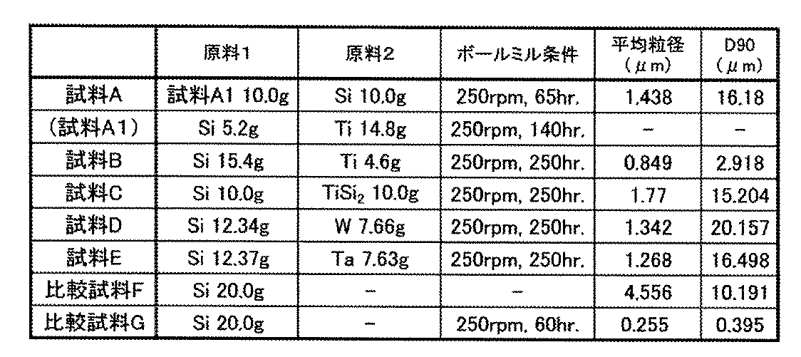
(負極の作製)
得られた試料A乃至試料E、比較試料F、比較試料Gを用いて、以下の方法により電極を作製した。すなわち、電極集電体として表面にニッケルを塗布した厚さ10μmのステンレス箔を用い、複合体粒子またはSi粒子、アセチレンブラック、及び結着剤であるポリイミド(より正確には、ポリイミドの前駆体)の混合比率を、80:5:15(重量%)としたものを、遊星型混練機を用いて混合することでスラリーを作製した。溶媒は、NMPを用いた。まず、複合体粒子またはSi粒子及びアセチレンブラックに溶媒であるNMPを添加して固練りを行った。次に、ポリイミドの前駆体およびNMPを添加して混練機で混合を行った。混練条件は、回転数2000rpm、5分として、固練りを含めて7回の混練を行った。次にブレード法を用いて集電体にスラリーを塗布した。ブレードの操作速度は10mm/secとした。空気雰囲気下で50℃、1時間乾燥してNMPを気化させた。次にポリイミドの前駆体をイミド化するために、窒素雰囲気で400℃、5時間の加熱処理を行った。 (Preparation of negative electrode)
Using the obtained Sample A to Sample E, Comparative Sample F, and Comparative Sample G, an electrode was produced by the following method. That is, a 10 μm-thick stainless steel foil with nickel coated on the surface is used as an electrode current collector, composite particles or Si particles, acetylene black, and a polyimide as a binder (more precisely, a precursor of polyimide) The mixture was mixed at 80: 5: 15 (% by weight) using a planetary kneader to prepare a slurry. NMP was used as the solvent. First, NMP, which is a solvent, was added to the composite particles or Si particles and acetylene black and kneaded. Next, a polyimide precursor and NMP were added and mixed with a kneader. The kneading conditions were such that the number of rotations was 2000 rpm, 5 minutes, and kneading was performed 7 times including solid kneading. Next, the slurry was apply | coated to the electrical power collector using the blade method. The operation speed of the blade was 10 mm / sec. NMP was vaporized by drying at 50 ° C. for 1 hour in an air atmosphere. Next, in order to imidize the polyimide precursor, a heat treatment was performed at 400 ° C. for 5 hours in a nitrogen atmosphere.
以上のようにして、各試料を有する負極を作製した。なお、試料A以外の各試料については、それぞれ担持量の異なる2種類の負極を作製した。試料Aを用いて作製した負極を負極Aとする。試料Bを用いて作製した2種類の負極を、それぞれ負極B1、負極B2とする。同様に、試料C、試料D、試料E、比較試料F、比較試料Gのそれぞれを用いて作製した2種類の負極を、それぞれ負極C1、負極C2、負極D1、負極D2、負極E1、負極E2、比較用負極F1、比較用負極F2、比較用負極G1、比較用負極G2とする。表2に、各負極における試料の担持量を示す。
In this way, a negative electrode having each sample was produced. For each sample other than sample A, two types of negative electrodes having different loadings were prepared. The negative electrode produced using Sample A is referred to as Negative Electrode A. Two types of negative electrodes prepared using Sample B are referred to as a negative electrode B1 and a negative electrode B2, respectively. Similarly, two types of negative electrodes prepared using Sample C, Sample D, Sample E, Comparative Sample F, and Comparative Sample G are respectively referred to as negative electrode C1, negative electrode C2, negative electrode D1, negative electrode D2, negative electrode E1, and negative electrode E2. Comparative negative electrode F1, comparative negative electrode F2, comparative negative electrode G1, and comparative negative electrode G2. Table 2 shows the loading amount of the sample in each negative electrode.

(セルの作製)
次に上記のように作製した各負極を用いて、ハーフセルを作製した。特性の評価は、CR2032タイプ(直径20mm高さ3.2mm)のコイン形蓄電池を用いた。対極には金属リチウム、セパレータにはポリプロピレンを用いた。電解液には、溶質として1Mol/lのLiPF6を用い、溶媒としてECとDECを体積比3:7で混合したものを用いた。負極A、負極B1、負極C1、負極D1、負極E1、比較用負極F1、比較用負極G1を用いて作製したハーフセルをそれぞれセルA、セルB1、セルC1、セルD1、セルE1、セルF1、セルG1とし、低担持量セルとよぶ。また、負極B2、負極C2、負極D2、負極E2、比較用負極F2、比較用負極G2を用いて作製したハーフセルをそれぞれセルB2、セルC2、セルD2、セルE2、セルF2、セルG2とし、高担持量セルとよぶ。 (Manufacture of cells)
Next, a half cell was produced using each negative electrode produced as described above. For the evaluation of the characteristics, a coin type storage battery of CR2032 type (diameter 20 mm, height 3.2 mm) was used. Metal lithium was used for the counter electrode and polypropylene was used for the separator. As the electrolytic solution, 1 mol / l LiPF 6 was used as a solute, and EC and DEC were mixed at a volume ratio of 3: 7 as a solvent. A half cell produced by using the negative electrode A, the negative electrode B1, the negative electrode C1, the negative electrode D1, the negative electrode E1, the comparative negative electrode F1, and the comparative negative electrode G1 is cell A, cell B1, cell C1, cell D1, cell E1, cell F1, This is referred to as cell G1 and is referred to as a low loading cell. Moreover, the half cell produced using the negative electrode B2, the negative electrode C2, the negative electrode D2, the negative electrode E2, the negative electrode for comparison F2, and the negative electrode for comparison G2 is designated as cell B2, cell C2, cell D2, cell E2, cell F2, and cell G2, respectively. This is called a high load cell.
次に上記のように作製した各負極を用いて、ハーフセルを作製した。特性の評価は、CR2032タイプ(直径20mm高さ3.2mm)のコイン形蓄電池を用いた。対極には金属リチウム、セパレータにはポリプロピレンを用いた。電解液には、溶質として1Mol/lのLiPF6を用い、溶媒としてECとDECを体積比3:7で混合したものを用いた。負極A、負極B1、負極C1、負極D1、負極E1、比較用負極F1、比較用負極G1を用いて作製したハーフセルをそれぞれセルA、セルB1、セルC1、セルD1、セルE1、セルF1、セルG1とし、低担持量セルとよぶ。また、負極B2、負極C2、負極D2、負極E2、比較用負極F2、比較用負極G2を用いて作製したハーフセルをそれぞれセルB2、セルC2、セルD2、セルE2、セルF2、セルG2とし、高担持量セルとよぶ。 (Manufacture of cells)
Next, a half cell was produced using each negative electrode produced as described above. For the evaluation of the characteristics, a coin type storage battery of CR2032 type (
(セルの測定)
次に、上記のように作製した各種セルの充放電特性およびサイクル特性の測定結果について示す。 (Cell measurement)
Next, measurement results of charge / discharge characteristics and cycle characteristics of the various cells produced as described above will be described.
次に、上記のように作製した各種セルの充放電特性およびサイクル特性の測定結果について示す。 (Cell measurement)
Next, measurement results of charge / discharge characteristics and cycle characteristics of the various cells produced as described above will be described.
ハーフセルの測定条件について説明する。充放電の方式は、初回の充放電のみ0.1Cのレートで定電流−定電圧充電および定電流放電を行い、2回目以降は0.2Cのレートで定電流−定電圧充電および定電流放電を行った。充放電の上限電圧を1.5V、下限電圧は0.01Vとした。また、測定温度は25℃で行った。なお、活物質のレートは、各種低担持量セルおよび比較試料を含む高担持量セル(セルF2、セルG2)は試料の担持量あたり4190mAh/gを基準として算出し、セルB2乃至セルE2は試料の担持量あたり2000mAh/gを基準として算出している。放電レート及び充電レートについて説明する。放電レートとは、電池容量に対する放電時の電流の相対的な比率であり、単位Cで表される。定格容量X(Ah)の電池において、1C相当の電流は、X(A)である。2X(A)の電流で放電させた場合は、2Cで放電させたといい、X/5(A)の電流で放電させた場合は、0.2Cで放電させたという。また、充電レートも同様であり、2X(A)の電流で充電させた場合は、2Cで充電させたといい、X/5(A)の電流で充電させた場合は、0.2Cで充電させたという。
Describe the measurement conditions for half-cells. The charge / discharge method is constant current-constant voltage charge and constant current discharge at a rate of 0.1 C only for the first charge / discharge, and constant current-constant voltage charge and constant current discharge at a rate of 0.2 C for the second and subsequent times. Went. The upper limit voltage of charging / discharging was 1.5V, and the lower limit voltage was 0.01V. The measurement temperature was 25 ° C. The rate of the active material is calculated based on 4190 mAh / g per sample loading of the high loading cell (cell F2, cell G2) including various low loading cells and comparative samples, and the cells B2 to E2 are The calculation is based on 2000 mAh / g per sample loading. A discharge rate and a charge rate will be described. The discharge rate is the relative ratio of the current during discharge to the battery capacity, and is expressed in units C. In a battery with a rated capacity X (Ah), the current corresponding to 1 C is X (A). When discharged at a current of 2X (A), it is said that it was discharged at 2C, and when discharged at a current of X / 5 (A), it was discharged at 0.2C. The charging rate is also the same. When charging with a current of 2X (A), it is said to be charged at 2C. When charging with a current of X / 5 (A), it is charged at 0.2C. It was said.
表3に、低担持量セル(セルA、セルB1乃至セルF1)の充放電の結果得られた初回の放電容量、初回の放電容量に対する10サイクル後の容量維持率、および初回の放電容量に対する20サイクル後の容量維持率を示す。
Table 3 shows the initial discharge capacity obtained as a result of the charge / discharge of the low supported amount cells (cell A, cell B1 to cell F1), the capacity retention rate after 10 cycles with respect to the initial discharge capacity, and the initial discharge capacity. The capacity retention rate after 20 cycles is shown.

また、図24および図25に低担持量セルの初回(1st cycle)および2回目(2nd cycle)の充放電カーブ(充放電特性とも呼ぶ)を示す。具体的には、図24(A)はセルF1の、図24(B)はセルG1の、図24(C)はセルAの、図24(D)はセルB1の、図25(A)はセルC1の、図25(B)はセルD1の、図25(C)はセルE1の充放電カーブである。
FIG. 24 and FIG. 25 show the first (1st cycle) and second (2nd cycle) charge / discharge curves (also referred to as charge / discharge characteristics) of the low loading amount cell. Specifically, FIG. 24A shows the cell F1, FIG. 24B shows the cell G1, FIG. 24C shows the cell A, FIG. 24D shows the cell B1, and FIG. FIG. 25B is a charge / discharge curve of the cell C1, FIG. 25B is a charge / discharge curve of the cell D1, and FIG.
図24および図25は、横軸が容量(mAh/g)であり、縦軸が電圧(V)である。初回の充放電カーブを実線で、2回目の充放電カーブを破線で示す。なお、図24(A)、(B)の横軸の目盛は図24(C)、(D)、図25(A)乃至(C)と異なる。
24 and 25, the horizontal axis represents capacity (mAh / g), and the vertical axis represents voltage (V). The first charge / discharge curve is indicated by a solid line, and the second charge / discharge curve is indicated by a broken line. 24A and 24B are different from those in FIGS. 24C and 24D and FIGS. 25A to 25C.
また、図26に低担持量セルの初回放電容量を100%とした場合の容量維持率の推移を示す。セルAの結果を太い実線で、セルB1の結果を細い実線で、セルC1の結果を一点鎖線で、セルD1の結果を二点鎖線で、セルE1の結果を破線で、セルF1の結果を細い点線で、セルG1の結果を太い点線で表す。
FIG. 26 shows the transition of the capacity retention rate when the initial discharge capacity of the low load cell is 100%. The result of cell A is a thick solid line, the result of cell B1 is a thin solid line, the result of cell C1 is a one-dot chain line, the result of cell D1 is a two-dot chain line, the result of cell E1 is a broken line, and the result of cell F1 is The thin dotted line represents the result of the cell G1 with a thick dotted line.
続いて、表4に高担持量セル(セルB2乃至セルF2)の充放電の結果得られた初回の放電容量、初回の放電容量に対する10サイクル後の容量維持率、および初回の放電容量に対する20サイクル後の容量維持率を示す。なお、セルC2およびセルD2の20サイクル後の容量維持率は測定中のため記載していない。
Subsequently, Table 4 shows the initial discharge capacity obtained as a result of charging / discharging of the high load amount cells (cell B2 to cell F2), the capacity maintenance rate after 10 cycles with respect to the initial discharge capacity, and 20 with respect to the initial discharge capacity. The capacity retention rate after cycling is shown. Note that the capacity retention ratios after 20 cycles of the cell C2 and the cell D2 are not described because they are being measured.

また、図27に高担持量セルの初回放電容量を100%とした場合の容量維持率の推移を示す。セルB2の結果を細い実線で、セルC2の結果を一点鎖線で、セルD2の結果を二点鎖線で、セルE2の結果を破線で、セルF2の結果を細い点線で、セルG2の結果を太い点線で表す。なお、セルC2およびセルD2の11サイクル以降の容量維持率は測定中のため記載していない。
FIG. 27 shows the transition of the capacity retention rate when the initial discharge capacity of the high load cell is 100%. The result of cell B2 is indicated by a thin solid line, the result of cell C2 is indicated by a one-dot chain line, the result of cell D2 is indicated by a two-dot chain line, the result of cell E2 is indicated by a broken line, the result of cell F2 is indicated by a thin dotted line, and the result of cell G2 is indicated. Represented by a thick dotted line. Note that the capacity retention rates of the cell C2 and the cell D2 after 11 cycles are not described because they are being measured.
表2、表3、図26および図27より、複合体を有する試料A乃至試料Eを負極に用いることで、膨張収縮に伴う活物質の変質及び電解液との副反応が抑制され、蓄電装置の容量維持率を高めることができることが示された。すなわち、本発明の一態様の蓄電装置用負極を用いることで、蓄電装置の容量維持率を高めることができる。
From Table 2, Table 3, FIG. 26, and FIG. 27, the use of Sample A to Sample E having the composite as the negative electrode suppresses the deterioration of the active material and the side reaction with the electrolytic solution that accompany expansion and contraction. It was shown that the capacity maintenance rate of can be increased. That is, by using the negative electrode for a power storage device of one embodiment of the present invention, the capacity retention rate of the power storage device can be increased.
以下の実施例では、実施例1と異なる負極を用いてハーフセルを作製し、サイクル特性の評価を行った。
In the following examples, a half cell was produced using a negative electrode different from that in Example 1, and the cycle characteristics were evaluated.
(複合体および比較試料の作製)
複合体の微粒子の作製を行った。まず、粒径45μmのチタン粉末を14.8g、および粒径5μmのシリコン粉末を5.2g秤量する。遊星回転方式ボールミル型粉砕機(LP−4、伊藤製作所製)付属の粉砕容器(クロム製、容量500ml)に、秤量したチタン粉末、シリコン粉末およびメディアを投入する。メディアは直径10mmのクロム鋼球であり、分量は粉砕容器に対して1/3を占める容積分(50個、約200g)である。粉砕容器内をアルゴン雰囲気とし、回転数250rpmで自転公転攪拌を行うことで試料H1の複合体を作製した。この時の処理時間は140時間であるが、処理中に何度か試料を粉砕容器から取り出し、撹拌を行った。続いて、試料H1を10.0g、および粒径5μmのシリコン粉末を10.0g秤量し、上記と同様の条件で65時間の自転公転攪拌を行うことで試料Hの複合体を作製した。 (Production of composite and comparative sample)
Composite fine particles were prepared. First, 14.8 g of titanium powder having a particle size of 45 μm and 5.2 g of silicon powder having a particle size of 5 μm are weighed. Weighed titanium powder, silicon powder, and media are put into a grinding container (made of chromium,capacity 500 ml) attached to a planetary rotation type ball mill type grinding machine (LP-4, manufactured by Ito Seisakusho). The medium is a chromium steel ball having a diameter of 10 mm, and the amount is a volume (50 pieces, approximately 200 g) occupying 1/3 of the grinding container. The composite of sample H1 was produced by carrying out rotation revolution stirring at the rotation speed of 250 rpm by making the inside of a grinding | pulverization container into argon atmosphere. The treatment time at this time is 140 hours, but the sample was taken out from the pulverization container several times during the treatment and stirred. Subsequently, 10.0 g of sample H1 and 10.0 g of silicon powder having a particle size of 5 μm were weighed, and a composite of sample H was prepared by performing rotation and revolution stirring for 65 hours under the same conditions as described above.
複合体の微粒子の作製を行った。まず、粒径45μmのチタン粉末を14.8g、および粒径5μmのシリコン粉末を5.2g秤量する。遊星回転方式ボールミル型粉砕機(LP−4、伊藤製作所製)付属の粉砕容器(クロム製、容量500ml)に、秤量したチタン粉末、シリコン粉末およびメディアを投入する。メディアは直径10mmのクロム鋼球であり、分量は粉砕容器に対して1/3を占める容積分(50個、約200g)である。粉砕容器内をアルゴン雰囲気とし、回転数250rpmで自転公転攪拌を行うことで試料H1の複合体を作製した。この時の処理時間は140時間であるが、処理中に何度か試料を粉砕容器から取り出し、撹拌を行った。続いて、試料H1を10.0g、および粒径5μmのシリコン粉末を10.0g秤量し、上記と同様の条件で65時間の自転公転攪拌を行うことで試料Hの複合体を作製した。 (Production of composite and comparative sample)
Composite fine particles were prepared. First, 14.8 g of titanium powder having a particle size of 45 μm and 5.2 g of silicon powder having a particle size of 5 μm are weighed. Weighed titanium powder, silicon powder, and media are put into a grinding container (made of chromium,
次に、比較試料の作製方法について説明する。比較試料Iは、粒径5μmのシリコン粉末である。比較試料Jは、粒径5μmのシリコン粉末を20.0g秤量し、上記と同様の条件で60時間の自転公転攪拌を行うことで作製した。なお、比較試料Jの作製において、自転公転攪拌を20時間行うごとに試料を粉砕容器から取り出し、撹拌を行った。
Next, a method for producing a comparative sample will be described. Comparative sample I is a silicon powder having a particle size of 5 μm. Comparative sample J was prepared by weighing 20.0 g of silicon powder having a particle size of 5 μm and performing rotation and revolution stirring for 60 hours under the same conditions as described above. In the preparation of the comparative sample J, the sample was taken out of the pulverization container and stirred every time the rotation and revolution stirring was performed for 20 hours.
表5に、各試料の作製に用いた原料、上記粉砕機による加工条件ならびに平均粒径およびD90の値を示す。粒径はレーザ回折粒度分布測定装置(SALD−2200形、島津製作所製)を用いて測定した。また、粒度の算出方式にはレーザ回折・散乱法を用いた。レーザ回折・散乱法の場合は、球形と仮定して得られる理想的回折パターンと、実測回折パターンを適合させて有効径を算出している。
Table 5 shows the raw materials used for the preparation of each sample, the processing conditions by the pulverizer, the average particle diameter, and the value of D90. The particle size was measured using a laser diffraction particle size distribution analyzer (SALD-2200, manufactured by Shimadzu Corporation). In addition, a laser diffraction / scattering method was used as a particle size calculation method. In the case of the laser diffraction / scattering method, an effective diameter is calculated by fitting an ideal diffraction pattern obtained assuming a spherical shape and an actually measured diffraction pattern.

(負極の作製)
得られた試料H、比較試料I、比較試料Jを用いて、以下の方法により電極を作製した。すなわち、電極集電体として表面にニッケルを塗布した厚さ10μmのステンレス箔を用い、複合体粒子またはSi粒子、アセチレンブラック、及び結着剤であるポリイミド(より正確には、ポリイミドの前駆体)の混合比率を、80:5:15(重量%)としたものを、遊星型混練機を用いて混合することでスラリーを作製した。溶媒は、NMPを用いた。まず、複合体粒子またはSi粒子及びアセチレンブラックに溶媒であるNMPを添加して固練りを行った。次に、ポリイミドの前駆体およびNMPを添加して混練機で混合を行った。混練条件は、回転数2000rpm、5分として、固練りを含めて7回の混練を行った。次にブレード法を用いて集電体にスラリーを塗布した。ブレードの操作速度は10mm/secとした。空気下で50℃、1時間乾燥してNMPを気化させた。次にポリイミドの前駆体をイミド化するために、窒素雰囲気で400℃、5時間の加熱処理を行った。 (Preparation of negative electrode)
Using the obtained sample H, comparative sample I, and comparative sample J, an electrode was produced by the following method. That is, a 10 μm-thick stainless steel foil having nickel coated on the surface is used as an electrode current collector, composite particles or Si particles, acetylene black, and a polyimide as a binder (more precisely, a precursor of polyimide) The mixture was mixed at 80: 5: 15 (% by weight) using a planetary kneader to prepare a slurry. NMP was used as the solvent. First, NMP, which is a solvent, was added to the composite particles or Si particles and acetylene black and kneaded. Next, a polyimide precursor and NMP were added and mixed with a kneader. The kneading conditions were such that the number of rotations was 2000 rpm, 5 minutes, and kneading was performed 7 times including solid kneading. Next, the slurry was apply | coated to the electrical power collector using the blade method. The operation speed of the blade was 10 mm / sec. NMP was vaporized by drying at 50 ° C. for 1 hour under air. Next, in order to imidize the polyimide precursor, a heat treatment was performed at 400 ° C. for 5 hours in a nitrogen atmosphere.
以上のようにして、試料H、比較試料I、比較試料Jを用いて作製した負極を、それぞれ負極H、比較用負極I、比較用負極Jとする。
The negative electrodes produced using Sample H, Comparative Sample I, and Comparative Sample J as described above are referred to as Negative Electrode H, Comparative Negative Electrode I, and Comparative Negative Electrode J, respectively.
各負極における試料の担持量は次の通りである。すなわち、負極Hにおける試料Hの担持量は、0.918mg/cm2、比較用負極Iにおける比較試料Iの担持量は0.829mg/cm2、比較用負極Jにおける比較試料Jの担持量は0.707mg/cm2である。
The loading amount of the sample in each negative electrode is as follows. That is, the loading amount of the sample H in the negative electrode H is 0.918 mg / cm 2 , the loading amount of the comparative sample I in the comparative negative electrode I is 0.829 mg / cm 2 , and the carrying amount of the comparative sample J in the comparative negative electrode J is 0.707 mg / cm 2 .
(セルの作製)
次に上記のように作製した負極H、比較用負極I、比較用負極Jを用いて、ハーフセルを作製した。特性の評価は、CR2032タイプ(直径20mm高さ3.2mm)のコイン形蓄電池を用いた。対極には金属リチウム、セパレータにはポリプロピレンを用いた。電解液には、溶質として1Mol/lのLiPF6を用い、溶媒としてECとDECを体積比3:7で混合したものを用いた。負極Hを用いて作製したハーフセルをセルH、比較用負極Iおよび比較用負極Jを用いて作製したハーフセルをそれぞれセルI、セルJとする。 (Manufacture of cells)
Next, a half cell was prepared using the negative electrode H, the comparative negative electrode I, and the comparative negative electrode J prepared as described above. For the evaluation of the characteristics, a coin type storage battery of CR2032 type (diameter 20 mm, height 3.2 mm) was used. Metal lithium was used for the counter electrode and polypropylene was used for the separator. As the electrolytic solution, 1 mol / l LiPF6 was used as a solute, and EC and DEC were mixed at a volume ratio of 3: 7 as a solvent. A half cell manufactured using the negative electrode H is referred to as a cell H, and a half cell manufactured using the comparative negative electrode I and the comparative negative electrode J is referred to as a cell I and a cell J, respectively.
次に上記のように作製した負極H、比較用負極I、比較用負極Jを用いて、ハーフセルを作製した。特性の評価は、CR2032タイプ(直径20mm高さ3.2mm)のコイン形蓄電池を用いた。対極には金属リチウム、セパレータにはポリプロピレンを用いた。電解液には、溶質として1Mol/lのLiPF6を用い、溶媒としてECとDECを体積比3:7で混合したものを用いた。負極Hを用いて作製したハーフセルをセルH、比較用負極Iおよび比較用負極Jを用いて作製したハーフセルをそれぞれセルI、セルJとする。 (Manufacture of cells)
Next, a half cell was prepared using the negative electrode H, the comparative negative electrode I, and the comparative negative electrode J prepared as described above. For the evaluation of the characteristics, a coin type storage battery of CR2032 type (
(セルの測定)
次に、上記のように作製したセルH乃至セルJの充放電特性およびサイクル特性の測定結果について示す。 (Cell measurement)
Next, measurement results of charge / discharge characteristics and cycle characteristics of the cells H to J manufactured as described above will be described.
次に、上記のように作製したセルH乃至セルJの充放電特性およびサイクル特性の測定結果について示す。 (Cell measurement)
Next, measurement results of charge / discharge characteristics and cycle characteristics of the cells H to J manufactured as described above will be described.
ハーフセルの測定条件について説明する。充放電の方式は、0.2Cのレートで定電流−定電圧充電とし、0.2Cのレートで定電流放電とした。充放電の上限電圧を1.5V、下限電圧は0.01Vとした。また、測定温度は25℃で行った。なお、シリコンおよびチタンを含む活物質のレートは試料の担持量あたり4190mAh/gを基準として算出している。
Describe the measurement conditions for half-cells. The charging / discharging method was constant current-constant voltage charging at a rate of 0.2C, and constant current discharging at a rate of 0.2C. The upper limit voltage of charging / discharging was 1.5V, and the lower limit voltage was 0.01V. The measurement temperature was 25 ° C. Note that the rate of the active material containing silicon and titanium is calculated based on 4190 mAh / g per sample loading.
また、サイクル特性の測定において、任意の1回の充放電と次の充放電との間には30分または2時間の体止時間を設けた。
Further, in the measurement of cycle characteristics, a body stoppage time of 30 minutes or 2 hours was provided between any one charge / discharge and the next charge / discharge.
表6に、セルF乃至セルHの充放電の結果得られた初回の放電容量、初回の放電容量に対する20サイクル後の容量維持率、および初回の放電容量に対する50サイクル後の容量維持率を示す。また、図28に初回放電容量を100%とした場合の容量維持率の推移を示す。セルHの結果は実線で、セルIの結果は点線で、セルJの結果は破線で表す。なお、セルJの21サイクル以降の容量維持率は測定中のため記載していない。
Table 6 shows the initial discharge capacity obtained as a result of charging and discharging of the cells F to H, the capacity maintenance ratio after 20 cycles with respect to the initial discharge capacity, and the capacity maintenance ratio after 50 cycles with respect to the initial discharge capacity. . FIG. 28 shows the transition of the capacity retention rate when the initial discharge capacity is 100%. The result of cell H is represented by a solid line, the result of cell I is represented by a dotted line, and the result of cell J is represented by a broken line. Note that the capacity retention rate of the cell J after 21 cycles is not described because it is being measured.

表5および図28より、本発明の一態様の蓄電装置用負極である負極活物質として複合体粒子を用いたセルHは、負極活物質としてシリコン粒子を用いたセルIおよびセルJよりも容量維持率が高いことがわかる。なお、セルIと比較してセルJの容量維持率が高いのは、比較試料Jの粒径が比較試料Iの粒径よりも小さいためである。
According to Table 5 and FIG. 28, the cell H using the composite particles as the negative electrode active material which is the negative electrode for a power storage device of one embodiment of the present invention has a capacity higher than those of the cells I and J using silicon particles as the negative electrode active material. It can be seen that the maintenance rate is high. The reason why the capacity retention rate of the cell J is higher than that of the cell I is that the particle size of the comparative sample J is smaller than the particle size of the comparative sample I.
(試料の断面観察)
図29に、比較試料Iの充放電前後の断面をSTEMで観察した結果を示す。図29(A)は比較用負極Iに担持する前の比較試料Iの断面像、図29(B)は50サイクルの充放電を行った後にセルIから取り出した比較試料Iの断面像である。また、図30に、試料Hの充放電前後の断面をSTEMで観察した結果を示す。図30(A)は負極Hに担持した状態の試料Hの断面像、図30(B)は50サイクルの充放電を行った後にセルHから取り出した試料Hの断面像である。なお、図29(A)と図29(B)は、それぞれ比較試料Iの別の領域の断面像である。同様に図30(A)と図30(B)は、それぞれ試料Hの別の領域の断面像である。 (Section observation of sample)
In FIG. 29, the result of having observed the cross section before and behind charge / discharge of the comparative sample I by STEM is shown. 29A is a cross-sectional image of the comparative sample I before being carried on the comparative negative electrode I, and FIG. 29B is a cross-sectional image of the comparative sample I taken out from the cell I after 50 cycles of charge / discharge. . FIG. 30 shows the result of observing the cross section of the sample H before and after charging and discharging with the STEM. 30A is a cross-sectional image of the sample H held on the negative electrode H, and FIG. 30B is a cross-sectional image of the sample H taken out from the cell H after 50 cycles of charge and discharge. 29A and 29B are cross-sectional images of different regions of the comparative sample I, respectively. Similarly, FIGS. 30A and 30B are cross-sectional images of different regions of the sample H, respectively.
比較試料Iでは、充放電を繰り返すことでシリコン粒子707の末端が枝状に変質しているが(図29(B)参照)、試料Hでは複合体703の変質が抑えられている(図30(B)参照)。これは、複合体粒子がシリサイドを含む第2の領域を有することで、充放電における複合体粒子の体積変化に伴い発生する応力や変質を緩和していることを示している。
In Comparative Sample I, the ends of the silicon particles 707 are altered into branches by repeating charging and discharging (see FIG. 29B), but in Sample H, alteration of the composite 703 is suppressed (FIG. 30). (See (B)). This indicates that the composite particles have the second region containing silicide, thereby relieving the stress and alteration caused by the volume change of the composite particles during charging and discharging.
本実施例では、電子線回折法によって、実施例1で作製した試料A乃至試料Eが有する複合体粒子の詳細を確認した結果について説明する。
In this example, the result of confirming the details of the composite particles included in Sample A to Sample E prepared in Example 1 by electron beam diffraction will be described.
前処理として、各試料をFIB(Focused Ion Beam System:集束イオンビーム加工観察装置)を用いて薄片化加工した後、透過型電子顕微鏡により断面の観察を行った。続いて、各断面像において点線で囲った2つまたは3つの領域(約0.3μmφ)について、電子線回折(ED:Electron Diffraction)測定を行った。
As pretreatment, each sample was processed into a thin piece using FIB (Focused Ion Beam System: focused ion beam processing observation apparatus), and then a cross section was observed with a transmission electron microscope. Subsequently, electron diffraction (ED: Electron Diffraction) measurement was performed on two or three regions (about 0.3 μmφ) surrounded by a dotted line in each cross-sectional image.
(試料AのED測定結果)
図31(A)に試料Aが有する複合体の断面TEM観察結果を示す。また図31(B)、(C)、(D)はそれぞれ、図31(A)の領域a1、領域a2、領域a3における電子線回折測定結果である。領域a1、領域a2は、図31(A)において縞状または格子状に観察された領域である。 (ED measurement result of sample A)
FIG. 31A shows a cross-sectional TEM observation result of the composite included in Sample A. FIG. FIGS. 31B, 31C, and 31D are electron beam diffraction measurement results in the regions a1, a2, and a3 in FIG. 31A, respectively. Regions a1 and a2 are regions observed in a striped pattern or a lattice pattern in FIG.
図31(B)の回折パターンより、回折スポットAの格子面間隔(d値ともいう)は0.225nm、回折スポットBのd値は0.223nm、回折スポットCのd値は0.209nmであることがわかった。また、面角度∠AOBは65°、∠BOCは57°、∠AOCは122°であることがわかった。また、データベースのTiSi2(71−0187)の[0 1 0]入射から得られる(3 1 −1)のd値は0.230nm、(3 −1 1)のd値は0.229nm、(0 −2 2)のd値は0.209nmであり、∠AOBは67°、∠BOCは56°、∠AOCは123°である。
From the diffraction pattern of FIG. 31B, the lattice spacing (also referred to as d value) of the diffraction spot A is 0.225 nm, the d value of the diffraction spot B is 0.223 nm, and the d value of the diffraction spot C is 0.209 nm. I found out. It was also found that the face angle ∠AOB was 65 °, ∠BOC was 57 °, and ∠AOC was 122 °. The d value of (3 1 -1) obtained from [0 1 0] incidence of TiSi 2 (71-0187) in the database is 0.230 nm, the d value of (3 −1 1) is 0.229 nm, ( The d value of 0 -2 2) is 0.209 nm, ∠AOB is 67 °, ∠BOC is 56 °, and ∠AOC is 123 °.
図31(B)の結果から得られた値と、データベースの値とを照合することにより、領域a1は結晶性のTiSi2を含むことが示唆された。
By collating the value obtained from the result of FIG. 31B with the value in the database, it was suggested that the region a1 contains crystalline TiSi 2 .
また、図31(C)の回折パターンより、回折スポットAのd値は0.254nm、回折スポットBのd値は0.184nm、回折スポットCのd値は0.225nmであることがわかった。また、面角度∠AOBは53°、∠BOCは45°、∠AOCは98°であることがわかった。また、データベースのTiSi2(71−0187)の[0 1 0]入射から得られる(2 1 −2)のd値は0.252nm、(3 −1 −3)のd値は0.182nm、(1 −2 −1)のd値は0.221nmであり、∠AOBは54°、∠BOCは46°、∠AOCは100°である。
Further, from the diffraction pattern of FIG. 31C, it was found that the d value of the diffraction spot A was 0.254 nm, the d value of the diffraction spot B was 0.184 nm, and the d value of the diffraction spot C was 0.225 nm. . It was also found that the surface angle ∠AOB was 53 °, ∠BOC was 45 °, and ∠AOC was 98 °. Moreover, d value of (2 1 -2) obtained from [0 1 0] incidence of TiSi 2 (71-0187) in the database is 0.252 nm, d value of (3 −1 -3) is 0.182 nm, The d value of (1-2-1) is 0.221 nm, ∠AOB is 54 °, ∠BOC is 46 °, and ∠AOC is 100 °.
図31(C)の結果から得られた値と、データベースの値とを照合することにより、領域a2は結晶性のTiSi2を含むことが示唆された。
By collating the value obtained from the result of FIG. 31C with the value of the database, it was suggested that the region a2 contains crystalline TiSi 2 .
一方で、図31(D)の回折パターンはハローパターンが主であるため、領域a3は結晶性が低いと考えられる。また、実施例1で示す試料AのXRD分析結果より、試料Aにおいて存在するTiSi2は結晶性を有し、Siは結晶性が低い。よって、領域a3は非晶質Siを含む可能性が高いと考えられる。なお、領域a3に非晶質のシリサイドが含まれる場合もある。
On the other hand, since the diffraction pattern in FIG. 31D is mainly a halo pattern, the region a3 is considered to have low crystallinity. Further, from the XRD analysis results of the sample A shown in Example 1, TiSi 2 present in the sample A has a crystalline, Si has low crystallinity. Therefore, it is considered that the region a3 is likely to contain amorphous Si. In some cases, the region a3 includes amorphous silicide.
以上の結果より、試料Aが有する複合体の断面TEM像において、縞状または格子状に観察される領域は、結晶性のシリサイドを含む第2の領域112、その他の領域は非晶質Siを含む第1の領域111または非晶質のシリサイドを含む第4の領域114であると考えられる。
From the above results, in the cross-sectional TEM image of the composite of sample A, the region observed in a striped or lattice shape is the second region 112 containing crystalline silicide, and the other regions are made of amorphous Si. It is considered that the first region 111 includes the fourth region 114 including amorphous silicide.
(試料BのED(Electron Diffraction)測定結果)
図32(A)に試料Bが有する複合体の断面TEM観察結果を示す。また図32(B)、(C)、(D)はそれぞれ、図32(A)の領域b1、領域b2、領域b3における電子線回折測定結果である。領域b1、領域b2は、図32(A)において縞状または格子状に観察された領域である。 (ED (Electron Diffraction) measurement result of sample B)
FIG. 32A shows a cross-sectional TEM observation result of the composite body included in Sample B. FIGS. 32B, 32C, and 32D show the results of electron beam diffraction measurement in the regions b1, b2, and b3 in FIG. 32A, respectively. Regions b1 and b2 are regions observed in a striped pattern or a lattice pattern in FIG.
図32(B)の回折パターンより、回折スポットAのd値は0.25nm、回折スポットBのd値は0.22nm、回折スポットCのd値は0.22nmであることがわかった。また、面角度∠AOBは55.0°、∠BOCは57.4°、∠AOCは112.4°であることがわかった。また、データベースのTiSi2(10−0225)の[5 1 4]入射から得られる(1 −1 −1)のd値は0.25nm、(1 −5 0)のd値は0.22nm、(0 −4 1)のd値は0.25nmであり、∠AOBは55.6°、∠BOCは54.8°、∠AOCは110.4°である。
From the diffraction pattern of FIG. 32B, it was found that the d value of the diffraction spot A was 0.25 nm, the d value of the diffraction spot B was 0.22 nm, and the d value of the diffraction spot C was 0.22 nm. Further, it was found that the surface angle ∠AOB was 55.0 °, ∠BOC was 57.4 °, and ∠AOC was 112.4 °. The d value of (1-1-1) obtained from [5 14] incidence of TiSi 2 (10-0225) in the database is 0.25 nm, and the d value of (1-50) is 0.22 nm, The d value of (0 -4 1) is 0.25 nm, ∠AOB is 55.6 °, ∠BOC is 54.8 °, and ∠AOC is 110.4 °.
図32(B)の結果から得られた値と、データベースの値とを照合することにより、領域b1は結晶性のTiSi2を含むことが示唆された。
By comparing the value obtained from the result of FIG. 32B with the value of the database, it was suggested that the region b1 contains crystalline TiSi 2 .
また、図32(C)の回折パターンより、回折スポットAのd値は0.22nm、回折スポットBのd値は0.15nm、回折スポットCのd値は0.22nmであることがわかった。また、面角度∠AOBは44.8°、∠BOCは43.9°、∠AOCは88.7°であることがわかった。また、データベースのTiSi2(10−0225)の[5 1 8]入射から得られる(1 3 −1)のd値は0.22nm、(2 −2 −1)のd値は0.16nm、(1 −5 0)のd値は0.22nmであり、∠AOBは45.9°、∠BOCは44.9°、∠AOCは90.8°である。
From the diffraction pattern of FIG. 32C, it was found that the d value of the diffraction spot A was 0.22 nm, the d value of the diffraction spot B was 0.15 nm, and the d value of the diffraction spot C was 0.22 nm. . Further, it was found that the surface angle ∠AOB was 44.8 °, ∠BOC was 43.9 °, and ∠AOC was 88.7 °. In addition, the d value of (1 3 -1) obtained from [5 1 8] incidence of TiSi 2 (10-0225) in the database is 0.22 nm, and the d value of (2 −2 −1) is 0.16 nm, The d value of (1 −50) is 0.22 nm, ∠AOB is 45.9 °, ∠BOC is 44.9 °, and ∠AOC is 90.8 °.
図32(C)の結果から得られた値と、データベースの値とを照合することにより、領域b2は結晶性のTiSi2を含むことが示唆された。
By collating the value obtained from the result of FIG. 32C with the value of the database, it was suggested that the region b2 contains crystalline TiSi 2 .
一方で、図32(D)の回折パターンは輝点が見られるもののハローパターンが主であるため、領域b3は結晶性が低いと考えられる。また、実施例1で示す試料BのXRD分析結果より、試料Bにおいて存在するTiSi2は結晶性を有し、Siは結晶性が低い。よって、領域b3は非晶質Siを含む可能性が高いと考えられる。なお、領域b3に非晶質のシリサイドが含まれる場合もある。
On the other hand, the diffraction pattern in FIG. 32D has a bright pattern, but mainly a halo pattern. Therefore, the region b3 is considered to have low crystallinity. From the XRD analysis result of Sample B shown in Example 1, TiSi 2 present in Sample B has crystallinity, and Si has low crystallinity. Therefore, it is considered that the region b3 is likely to contain amorphous Si. Note that the region b3 may include amorphous silicide.
以上の結果より、試料Bが有する複合体の断面TEM像において、縞状または格子状に観察される領域は結晶性のシリサイドを含む第2の領域112、その他の領域は非晶質Siを含む第1の領域111または非晶質のシリサイドを含む第4の領域114であると考えられる。
Based on the above results, in the cross-sectional TEM image of the composite of sample B, the region observed in a striped or lattice shape is the second region 112 containing crystalline silicide, and the other regions contain amorphous Si. The first region 111 or the fourth region 114 containing amorphous silicide is considered.
(試料CのED測定結果)
図33(A)に試料Bが有する複合体の断面TEM観察結果を示す。また図33(B)、(C)、(D)はそれぞれ、図33(A)の領域c1、領域c2、領域c3における電子線回折測定結果である。領域c1は、図33(A)において縞状または格子状に観察された領域である。 (ED measurement result of sample C)
FIG. 33A shows a cross-sectional TEM observation result of the composite included in Sample B. 33B, 33C, and 33D show the results of electron beam diffraction measurement in the regions c1, c2, and c3 in FIG. 33A, respectively. The region c1 is a region observed in a stripe shape or a lattice shape in FIG.
図33(B)の回折パターンより、回折スポットAのd値は0.19nm、回折スポットBのd値は0.14nm、回折スポットCのd値は0.24nmであることがわかった。また、面角度∠AOBは33.8°、∠BOCは44.6°、∠AOCは78.4°であることがわかった。また、データベースのTiSi2(10−0225)の[7 1 6]入射から得られる(0 6 −1)のd値は0.19nm、(1 5 2)のd値は0.14nm、(1 −1 1)のd値は0.25nmであり、∠AOBは32.7°、∠BOCは44.6°、∠AOCは77.3°である。
From the diffraction pattern of FIG. 33B, it was found that the d value of the diffraction spot A was 0.19 nm, the d value of the diffraction spot B was 0.14 nm, and the d value of the diffraction spot C was 0.24 nm. Further, it was found that the surface angle ∠AOB was 33.8 °, ∠BOC was 44.6 °, and ∠AOC was 78.4 °. Moreover, d value of (0 6 -1) obtained from [7 1 6] incidence of TiSi 2 (10-0225) in the database is 0.19 nm, d value of (1 5 2) is 0.14 nm, (1 The d value of -1 1) is 0.25 nm, ∠AOB is 32.7 °, ∠BOC is 44.6 °, and ∠AOC is 77.3 °.
図33(B)の結果から得られた値と、データベースの値とを照合することにより、領域c1は結晶性のTiSi2を含むことが示唆された。
By comparing the value obtained from the result of FIG. 33B with the value of the database, it was suggested that the region c1 contains crystalline TiSi 2 .
一方で、図32(C)の回折パターンは輝点が見られるもののハローパターンが主であり、図32(D)の回折パターンもハローパターンが主であるため、領域c2および領域c3は結晶性が低いと考えられる。また、実施例1で示す試料CのXRD分析結果より、試料Cにおいて存在するTiSi2は結晶性を有し、Siは結晶性が低い。よって、領域c2および領域c3は非晶質Siを含む可能性が高いと考えられる。なお、領域c2または/および領域c3に非晶質のシリサイドが含まれる場合もある。
On the other hand, although the diffraction pattern in FIG. 32C is mainly a halo pattern with a bright spot, and the diffraction pattern in FIG. 32D is also mainly a halo pattern, the regions c2 and c3 are crystalline. Is considered low. Further, from the XRD analysis results of the samples C shown in Example 1, TiSi 2 present in the sample C has a crystalline, Si has low crystallinity. Therefore, it is considered that the region c2 and the region c3 are likely to contain amorphous Si. Note that amorphous silicide may be included in the region c2 and / or the region c3.
以上の結果より、試料Cが有する複合体の断面TEM像において、縞状または格子状に観察される領域は結晶性のシリサイドを含む第2の領域112、その他の領域は非晶質Siを含む第1の領域111または非晶質のシリサイドを含む第4の領域114であると考えられる。
From the above results, in the cross-sectional TEM image of the composite of sample C, the region observed in a striped or lattice shape is the second region 112 containing crystalline silicide, and the other regions contain amorphous Si. The first region 111 or the fourth region 114 containing amorphous silicide is considered.
(試料DのED測定結果)
図34(A)に試料Dが有する複合体の断面TEM観察結果を示す。また図34(B)、(C)はそれぞれ、図34(A)の領域d1、領域d2における電子線回折測定結果である。領域d1は、図34(A)において縞状または格子状に観察された領域である。 (ED measurement result of sample D)
FIG. 34A shows a cross-sectional TEM observation result of the composite body included in Sample D. FIG. 34B and 34C show the results of electron beam diffraction measurement in the region d1 and the region d2 in FIG. 34A, respectively. The region d1 is a region observed in a stripe shape or a lattice shape in FIG.
図34(B)の回折パターンより、回折スポットAのd値は0.21nm、回折スポットBのd値は0.10nm、回折スポットCのd値は0.13nmであることがわかった。また、面角度∠AOBは53.5°、∠BOCは30.4°、∠AOCは83.9°であることがわかった。また、データベースのWSi2(81−2168)の[3 9 1]入射から得られる(1 0 −3)のd値は0.20nm、(3 −1 0)のd値は0.10nm、(2 −1 3)のd値は0.13nmであり、∠AOBは53.2°、∠BOCは29.9°、∠AOCは83.1°である。
From the diffraction pattern of FIG. 34B, it was found that the d value of the diffraction spot A was 0.21 nm, the d value of the diffraction spot B was 0.10 nm, and the d value of the diffraction spot C was 0.13 nm. It was also found that the face angle ∠AOB was 53.5 °, ∠BOC was 30.4 °, and ∠AOC was 83.9 °. Further, the d value of (1 0 -3) obtained from [3 9 1] incidence of WSi 2 (81-2168) in the database is 0.20 nm, the d value of (3 -10) is 0.10 nm, ( The d value of 2 −1 3) is 0.13 nm, ∠AOB is 53.2 °, ∠BOC is 29.9 °, and ∠AOC is 83.1 °.
図34(B)の結果から得られた値と、データベースの値とを照合することにより、領域d1は結晶性のWSi2を含むことが示唆された。
By collating the value obtained from the result of FIG. 34B with the value of the database, it was suggested that the region d1 contains crystalline WSi 2 .
一方で、図34(C)の回折パターンはハローパターンが主であるため、領域d2は結晶性が低いと考えられる。また、実施例1で示す試料DのXRD分析結果より、試料Dにおいて存在するWSi2は結晶性を有し、Siは結晶性が低い。よって、領域d2は非晶質Siを含む可能性が高いと考えられる。なお、領域d2に非晶質のシリサイドが含まれる場合もある。
On the other hand, since the diffraction pattern in FIG. 34C is mainly a halo pattern, the region d2 is considered to have low crystallinity. Further, from the XRD analysis results of the sample D shown in Example 1, WSi 2 present in the sample D has a crystalline, Si has low crystallinity. Therefore, it is considered that the region d2 is likely to contain amorphous Si. Note that the region d2 may include amorphous silicide.
以上の結果より、試料Dが有する複合体の断面TEM像において、縞状または格子状に観察される領域は結晶性のシリサイドを含む第2の領域112、その他の領域は非晶質Siを含む第1の領域111または非晶質のシリサイドを含む第4の領域114であると考えられる。
Based on the above results, in the cross-sectional TEM image of the composite of sample D, the region observed in a striped or lattice shape is the second region 112 containing crystalline silicide, and the other regions contain amorphous Si. The first region 111 or the fourth region 114 containing amorphous silicide is considered.
(試料EのED測定結果)
図35(A)に試料Eが有する複合体の断面TEM観察結果を示す。また図35(B)、(C)、(D)はそれぞれ、図35(A)の領域e1、領域e2、領域e3における電子線回折測定結果である。領域e1、領域e2は、図35(A)において縞状または格子状に観察された領域である。 (ED measurement result of sample E)
FIG. 35A shows a cross-sectional TEM observation result of the composite included in Sample E. FIGS. 35B, 35C, and 35D are electron beam diffraction measurement results in region e1, region e2, and region e3 in FIG. 35A, respectively. Regions e1 and e2 are regions observed in a striped pattern or a lattice pattern in FIG.
図35(B)の回折パターンより、回折スポットAのd値は0.64nm、回折スポットBのd値は0.23nm、回折スポットCのd値は0.25nmであることがわかった。また、面角度∠AOBは71.3°、∠BOCは19.9°、∠AOCは91.2°であることがわかった。また、データベースのTaSi2(38−0483)の[1 2 0]入射から得られる(0 0 1)のd値は0.66nm、(−2 1 1)のd値は0.22nm、(−2 1 0)のd値は0.24nmであり、∠AOBは69.9°、∠BOCは20.1°、∠AOCは90.0°である。
From the diffraction pattern of FIG. 35B, it was found that the d value of the diffraction spot A was 0.64 nm, the d value of the diffraction spot B was 0.23 nm, and the d value of the diffraction spot C was 0.25 nm. Further, it was found that the surface angle ∠AOB was 71.3 °, ∠BOC was 19.9 °, and ∠AOC was 91.2 °. The d value of (0 0 1) obtained from [1 2 0] incidence of TaSi 2 (38-0383) in the database is 0.66 nm, the d value of (−2 1 1) is 0.22 nm, (− The d value of 2 1 0) is 0.24 nm, ∠AOB is 69.9 °, ∠BOC is 20.1 °, and ∠AOC is 90.0 °.
図35(B)の結果から得られた値と、データベースの値とを照合することにより、領域e1は結晶性のTaSi2を含むことが示唆された。
By collating the value obtained from the result of FIG. 35B with the value of the database, it was suggested that the region e1 contains crystalline TaSi 2 .
また、図35(C)の回折パターンより、回折スポットAのd値は0.23nm、回折スポットBのd値は0.14nm、回折スポットCのd値は0.25nmであることがわかった。また、面角度∠AOBは29.5°、∠BOCは30.7°、∠AOCは60.2°であることがわかった。また、データベースのTaSi2(38−0483)の[1 2 3]入射から得られる(1 1 −1)のd値は0.22nm、(3 0 −1)のd値は0.14nm、(2 −1 0)のd値は0.24nmであり、∠AOBは29.9°、∠BOCは32.1°、∠AOCは62.0°である。
Further, from the diffraction pattern of FIG. 35C, it was found that the d value of the diffraction spot A was 0.23 nm, the d value of the diffraction spot B was 0.14 nm, and the d value of the diffraction spot C was 0.25 nm. . Further, it was found that the surface angle ∠AOB was 29.5 °, ∠BOC was 30.7 °, and ∠AOC was 60.2 °. Further, the d value of (1 1 −1) obtained from [1 2 3] incidence of TaSi 2 (38-0383) in the database is 0.22 nm, the d value of (3 0 −1) is 0.14 nm, ( 2 −10) is 0.24 nm, 0.2AOB is 29.9 °, ∠BOC is 32.1 °, and ∠AOC is 62.0 °.
図35(C)の結果から得られた値と、データベースの値とを照合することにより、領域b2は結晶性のTaSi2を含むことが示唆された。
By collating the value obtained from the result of FIG. 35C with the value of the database, it was suggested that the region b2 contains crystalline TaSi 2 .
一方で、図35(D)の回折パターンはハローパターンが主であるため、領域e3は結晶性が低いと考えられる。また、実施例1で示す試料EのXRD分析結果より、試料Eにおいて存在するTaSi2は結晶性を有し、Siは結晶性が低い。よって、領域e3は非晶質Siを含む可能性が高いと考えられる。なお、領域e3に非晶質のシリサイドが含まれる場合もある。
On the other hand, since the diffraction pattern in FIG. 35D is mainly a halo pattern, the region e3 is considered to have low crystallinity. Moreover, from the XRD analysis result of the sample E shown in Example 1, TaSi 2 existing in the sample E has crystallinity, and Si has low crystallinity. Therefore, it is considered that the region e3 is likely to contain amorphous Si. Note that the region e3 may include amorphous silicide.
以上の結果より、試料Eが有する複合体の断面TEM像において、縞状または格子状に観察される領域は結晶性のシリサイドを含む第2の領域112、その他の領域は非晶質Siを含む第1の領域111または非晶質のシリサイドを含む第4の領域114であると考えられる。
From the above results, in the cross-sectional TEM image of the composite of sample E, the region observed in a striped or lattice shape is the second region 112 containing crystalline silicide, and the other regions contain amorphous Si. The first region 111 or the fourth region 114 containing amorphous silicide is considered.
100 負極
101 負極集電体
102 負極活物質層
103 複合体
104 導電助剤
105 結着剤
106 領域
111 第1の領域
112 第2の領域
113 第3の領域
114 第4の領域
200 負極
201 負極集電体
202 負極活物質層
204 グラフェン
300 蓄電池
301 正極缶
302 負極缶
303 ガスケット
304 正極
305 正極集電体
306 正極活物質層
307 負極
308 負極集電体
309 負極活物質層
310 セパレータ
400 蓄電池
402 正極
404 負極
500 蓄電池
501 正極集電体
502 正極活物質層
503 正極
504 負極集電体
505 負極活物質層
506 負極
507 セパレータ
508 電解液
509 外装体
510 正極リード電極
511 負極リード電極
512 溶接領域
513 湾曲部
514 封止部
600 蓄電池
601 正極キャップ
602 電池缶
603 正極端子
604 正極
605 セパレータ
606 負極
607 負極端子
608 絶縁板
609 絶縁板
611 PTC素子
612 安全弁機構
703 複合体
707 シリコン粒子
900 回路基板
910 ラベル
911 端子
912 回路
913 蓄電体
914 アンテナ
915 アンテナ
916 層
917 層
918 アンテナ
919 端子
920 表示装置
921 センサ
922 端子
951 端子
952 端子
981 フィルム
982 フィルム
990 蓄電装置
991 外装体
992 外装体
993 捲回体
994 負極
995 正極
996 セパレータ
997 リード電極
998 リード電極
7100 携帯表示装置
7101 筐体
7102 表示部
7103 操作ボタン
7104 蓄電装置
7105 リード電極
7106 集電体
7200 携帯情報端末
7201 筐体
7202 表示部
7203 バンド
7204 バックル
7205 操作ボタン
7206 入出力端子
7207 アイコン
7400 携帯電話機
7401 筐体
7402 表示部
7403 操作ボタン
7404 外部接続ポート
7405 スピーカ
7406 マイク
7407 蓄電装置
7408 リード電極
7409 集電体
8021 充電装置
8022 ケーブル
8100 自動車
8101 ヘッドライト
8106 電気モーター 100 Negative electrode 101 Negative electrode current collector 102 Negative electrode active material layer 103 Composite 104 Conductive aid 105 Binder 106 Region 111 First region 112 Second region 113 Third region 114 Fourth region 200 Negative electrode 201 Negative electrode collection Electrode 202 Negative electrode active material layer 204 Graphene 300 Storage battery 301 Positive electrode can 302 Negative electrode can 303 Gasket 304 Positive electrode 305 Positive electrode current collector 306 Positive electrode active material layer 307 Negative electrode 308 Negative electrode current collector 309 Negative electrode active material layer 310 Separator 400 Storage battery 402 Positive electrode 404 Negative electrode 500 Storage battery 501 Positive electrode current collector 502 Positive electrode active material layer 503 Positive electrode 504 Negative electrode current collector 505 Negative electrode active material layer 506 Negative electrode 507 Separator 508 Electrolyte 509 Exterior body 510 Positive electrode lead electrode 511 Negative electrode lead electrode 512 Welding region 513 Curve 514 Sealing unit 600 Storage battery 601 Positive electrode cap 602 Battery can 603 Positive electrode terminal 604 Positive electrode 605 Separator 606 Negative electrode 607 Negative electrode terminal 608 Insulating plate 609 Insulating plate 611 PTC element 612 Safety valve mechanism 703 Composite 707 Silicon particle 900 Circuit board 910 Label 911 Terminal 912 Circuit 913 Power storage unit 914 Antenna 915 Antenna 916 Layer 917 Layer 918 Antenna 919 Terminal 920 Display device 921 Sensor 922 Terminal 951 Terminal 952 Terminal 981 Film 982 Film 990 Power storage device 991 Exterior body 992 Exterior body 993 Winding body 994 Negative electrode 995 Positive electrode 996 Separator 997 Lead electrode 998 Lead electrode 7100 Portable display device 7101 Housing 7102 Display unit 7103 Operation button 7104 Power storage device 7105 Lead electrode 7106 Current collector 7200 Portable information terminal 7201 Case 7202 Display unit 7203 Band 7204 Buckle 7205 Operation button 7206 Input / output terminal 7207 Icon 7400 Mobile phone 7401 Case 7402 Display unit 7403 Operation button 7404 External connection port 7405 Speaker 7406 Microphone 7407 Power storage device 7408 Lead electrode 7409 Current collector 8021 Charging device 8022 Cable 8100 Car 8101 Headlight 8106 Electric motor
Claims (7)
- 多数の粒子状の複合体を備え、
前記複合体は、第1の領域と、第2の領域と、を有し、
前記第1の領域は、非晶質シリコンを含み、
前記第2の領域は、結晶性のシリサイドを含み、
前記第2の領域の端部は、前記第1の領域と重なる、
蓄電装置用負極。 With a large number of particulate composites,
The complex has a first region and a second region;
The first region comprises amorphous silicon;
The second region includes crystalline silicide,
An end of the second region overlaps the first region;
Negative electrode for power storage device. - 多数の粒子状の複合体を備え、
前記複合体は、第1の領域と、第2の領域と、を有し、
前記第1の領域は、非晶質シリコンを含み、
前記第2の領域は、結晶性のシリサイドを含み、
前記第2の領域は、前記第2の領域の端部において前記第1の領域と接する領域を有し、
前記第2の領域の端部近傍において、前記第2の領域は、前記第1の領域との距離が小さくなるにつれて結晶性が低下する、
蓄電装置用負極。 With a large number of particulate composites,
The complex has a first region and a second region;
The first region comprises amorphous silicon;
The second region includes crystalline silicide,
The second region has a region in contact with the first region at an end of the second region;
In the vicinity of the edge of the second region, the crystallinity of the second region decreases as the distance from the first region decreases.
Negative electrode for power storage device. - 請求項1または請求項2において、
前記結晶性のシリサイドは、チタン、タンタル、またはタングステンのいずれかを含む、
蓄電装置用負極。 In claim 1 or claim 2,
The crystalline silicide includes any of titanium, tantalum, or tungsten.
Negative electrode for power storage device. - 請求項1または請求項2において、
前記第2の領域の厚みは、1nm以上50nm以下である、
蓄電装置用負極。 In claim 1 or claim 2,
The thickness of the second region is 1 nm or more and 50 nm or less,
Negative electrode for power storage device. - 請求項3において、
チタン、タンタル、またはタングステンのいずれかに対するシリコンの原子数比が、2倍以上20倍以下である、
蓄電装置用負極。 In claim 3,
The atomic ratio of silicon to any of titanium, tantalum, or tungsten is 2 times or more and 20 times or less,
Negative electrode for power storage device. - 請求項1または請求項2に記載の蓄電装置用負極を有する蓄電装置。 A power storage device having the negative electrode for a power storage device according to claim 1 or 2.
- 請求項6に記載の蓄電装置を搭載した電気機器。 Electrical equipment equipped with the power storage device according to claim 6.
Applications Claiming Priority (2)
| Application Number | Priority Date | Filing Date | Title |
|---|---|---|---|
| JP2016095791 | 2016-05-12 | ||
| JP2016-095791 | 2016-05-12 |
Publications (1)
| Publication Number | Publication Date |
|---|---|
| WO2017195071A1 true WO2017195071A1 (en) | 2017-11-16 |
Family
ID=60266355
Family Applications (1)
| Application Number | Title | Priority Date | Filing Date |
|---|---|---|---|
| PCT/IB2017/052547 WO2017195071A1 (en) | 2016-05-12 | 2017-05-03 | Negative electrode to be used in power storage device, power storage device, and electrical device |
Country Status (1)
| Country | Link |
|---|---|
| WO (1) | WO2017195071A1 (en) |
Citations (6)
| Publication number | Priority date | Publication date | Assignee | Title |
|---|---|---|---|---|
| WO2006129415A1 (en) * | 2005-06-03 | 2006-12-07 | Matsushita Electric Industrial Co., Ltd. | Rechargeable battery with nonaqueous electrolyte and process for producing negative electrode |
| JP2009021046A (en) * | 2007-07-10 | 2009-01-29 | Panasonic Corp | Positive electrode material for nonaqueous electrolyte secondary battery, nonaqueous electrolyte secondary battery using the same, and method of manufacturing positive electrode material for nonaqueous electrolyte secondary battery |
| JP2009521792A (en) * | 2005-12-23 | 2009-06-04 | スリーエム イノベイティブ プロパティズ カンパニー | Silicon-containing alloys useful for lithium-ion battery electrodes |
| JP2013253012A (en) * | 2012-05-07 | 2013-12-19 | Furukawa Electric Co Ltd:The | Silicide combined silicon material and nonaqueous electrolyte secondary battery using the same |
| JP2014107132A (en) * | 2012-11-28 | 2014-06-09 | Furukawa Electric Co Ltd:The | Negative electrode material for lithium ion secondary battery, negative electrode for lithium ion secondary battery, lithium ion secondary battery, and method for producing negative electrode material for lithium ion secondary battery |
| JP2015125794A (en) * | 2013-12-25 | 2015-07-06 | 古河電気工業株式会社 | Composite particles and manufacturing method thereof, and negative electrode and nonaqueous electrolyte secondary battery using the same |
-
2017
- 2017-05-03 WO PCT/IB2017/052547 patent/WO2017195071A1/en active Application Filing
Patent Citations (6)
| Publication number | Priority date | Publication date | Assignee | Title |
|---|---|---|---|---|
| WO2006129415A1 (en) * | 2005-06-03 | 2006-12-07 | Matsushita Electric Industrial Co., Ltd. | Rechargeable battery with nonaqueous electrolyte and process for producing negative electrode |
| JP2009521792A (en) * | 2005-12-23 | 2009-06-04 | スリーエム イノベイティブ プロパティズ カンパニー | Silicon-containing alloys useful for lithium-ion battery electrodes |
| JP2009021046A (en) * | 2007-07-10 | 2009-01-29 | Panasonic Corp | Positive electrode material for nonaqueous electrolyte secondary battery, nonaqueous electrolyte secondary battery using the same, and method of manufacturing positive electrode material for nonaqueous electrolyte secondary battery |
| JP2013253012A (en) * | 2012-05-07 | 2013-12-19 | Furukawa Electric Co Ltd:The | Silicide combined silicon material and nonaqueous electrolyte secondary battery using the same |
| JP2014107132A (en) * | 2012-11-28 | 2014-06-09 | Furukawa Electric Co Ltd:The | Negative electrode material for lithium ion secondary battery, negative electrode for lithium ion secondary battery, lithium ion secondary battery, and method for producing negative electrode material for lithium ion secondary battery |
| JP2015125794A (en) * | 2013-12-25 | 2015-07-06 | 古河電気工業株式会社 | Composite particles and manufacturing method thereof, and negative electrode and nonaqueous electrolyte secondary battery using the same |
Similar Documents
| Publication | Publication Date | Title |
|---|---|---|
| US10249876B2 (en) | Lithium-ion secondary battery and electronic device | |
| US10454102B2 (en) | Lithium manganese composite oxide, secondary battery, electronic device, and method for forming layer | |
| JP2021180193A (en) | Secondary battery | |
| JP2023103453A (en) | Lithium-ion secondary battery | |
| JP6840476B2 (en) | How to make a power storage device | |
| JP6089008B2 (en) | Lithium manganese composite oxide, lithium ion secondary battery, and electrical equipment | |
| JP7146998B2 (en) | Composite for negative electrode | |
| US10593940B2 (en) | Negative electrode for power storage device, power storage, device and electrical device | |
| JP2015143176A (en) | Lithium manganese composite oxide, secondary battery, and electrical device | |
| US20210167353A1 (en) | Storage battery electrode, manufacturing method thereof, storage battery, and electronic device | |
| US9929408B2 (en) | Electrode member, secondary battery, and method for manufacturing electrode member | |
| JP2016001603A (en) | Negative electrode active material and power storage device | |
| US11637293B2 (en) | Method for manufacturing lithium-containing complex phosphate elliptical particles | |
| US20230343952A1 (en) | Secondary battery, manufacturing method of secondary battery, electronic device, and vehicle | |
| WO2017195071A1 (en) | Negative electrode to be used in power storage device, power storage device, and electrical device | |
| WO2022034414A1 (en) | Secondary battery, electronic device, vehicle, and method for producing positive electrode active material |
Legal Events
| Date | Code | Title | Description |
|---|---|---|---|
| NENP | Non-entry into the national phase |
Ref country code: DE |
|
| 121 | Ep: the epo has been informed by wipo that ep was designated in this application |
Ref document number: 17795700 Country of ref document: EP Kind code of ref document: A1 |
|
| 122 | Ep: pct application non-entry in european phase |
Ref document number: 17795700 Country of ref document: EP Kind code of ref document: A1 |
|
| NENP | Non-entry into the national phase |
Ref country code: JP |