WO2017188744A1 - Sers 센서용 기판의 평가방법 - Google Patents
Sers 센서용 기판의 평가방법 Download PDFInfo
- Publication number
- WO2017188744A1 WO2017188744A1 PCT/KR2017/004474 KR2017004474W WO2017188744A1 WO 2017188744 A1 WO2017188744 A1 WO 2017188744A1 KR 2017004474 W KR2017004474 W KR 2017004474W WO 2017188744 A1 WO2017188744 A1 WO 2017188744A1
- Authority
- WO
- WIPO (PCT)
- Prior art keywords
- substrate
- sers sensor
- nanoparticles
- raman signal
- color
- Prior art date
- Legal status (The legal status is an assumption and is not a legal conclusion. Google has not performed a legal analysis and makes no representation as to the accuracy of the status listed.)
- Ceased
Links
Images
Classifications
-
- G—PHYSICS
- G01—MEASURING; TESTING
- G01N—INVESTIGATING OR ANALYSING MATERIALS BY DETERMINING THEIR CHEMICAL OR PHYSICAL PROPERTIES
- G01N21/00—Investigating or analysing materials by the use of optical means, i.e. using sub-millimetre waves, infrared, visible or ultraviolet light
- G01N21/62—Systems in which the material investigated is excited whereby it emits light or causes a change in wavelength of the incident light
- G01N21/63—Systems in which the material investigated is excited whereby it emits light or causes a change in wavelength of the incident light optically excited
- G01N21/65—Raman scattering
- G01N21/658—Raman scattering enhancement Raman, e.g. surface plasmons
-
- G—PHYSICS
- G01—MEASURING; TESTING
- G01N—INVESTIGATING OR ANALYSING MATERIALS BY DETERMINING THEIR CHEMICAL OR PHYSICAL PROPERTIES
- G01N21/00—Investigating or analysing materials by the use of optical means, i.e. using sub-millimetre waves, infrared, visible or ultraviolet light
- G01N21/17—Systems in which incident light is modified in accordance with the properties of the material investigated
- G01N21/55—Specular reflectivity
- G01N21/552—Attenuated total reflection
- G01N21/553—Attenuated total reflection and using surface plasmons
- G01N21/554—Attenuated total reflection and using surface plasmons detecting the surface plasmon resonance of nanostructured metals, e.g. localised surface plasmon resonance
-
- G—PHYSICS
- G01—MEASURING; TESTING
- G01N—INVESTIGATING OR ANALYSING MATERIALS BY DETERMINING THEIR CHEMICAL OR PHYSICAL PROPERTIES
- G01N21/00—Investigating or analysing materials by the use of optical means, i.e. using sub-millimetre waves, infrared, visible or ultraviolet light
- G01N21/17—Systems in which incident light is modified in accordance with the properties of the material investigated
- G01N21/25—Colour; Spectral properties, i.e. comparison of effect of material on the light at two or more different wavelengths or wavelength bands
- G01N21/255—Details, e.g. use of specially adapted sources, lighting or optical systems
-
- G—PHYSICS
- G01—MEASURING; TESTING
- G01Q—SCANNING-PROBE TECHNIQUES OR APPARATUS; APPLICATIONS OF SCANNING-PROBE TECHNIQUES, e.g. SCANNING PROBE MICROSCOPY [SPM]
- G01Q60/00—Particular types of SPM [Scanning Probe Microscopy] or microscopes; Essential components thereof
- G01Q60/02—Multiple-type SPM, i.e. involving more than one SPM techniques
- G01Q60/04—STM [Scanning Tunnelling Microscopy] combined with AFM [Atomic Force Microscopy]
-
- G—PHYSICS
- G01—MEASURING; TESTING
- G01N—INVESTIGATING OR ANALYSING MATERIALS BY DETERMINING THEIR CHEMICAL OR PHYSICAL PROPERTIES
- G01N21/00—Investigating or analysing materials by the use of optical means, i.e. using sub-millimetre waves, infrared, visible or ultraviolet light
- G01N21/17—Systems in which incident light is modified in accordance with the properties of the material investigated
- G01N21/25—Colour; Spectral properties, i.e. comparison of effect of material on the light at two or more different wavelengths or wavelength bands
- G01N2021/258—Surface plasmon spectroscopy, e.g. micro- or nanoparticles in suspension
-
- G—PHYSICS
- G01—MEASURING; TESTING
- G01N—INVESTIGATING OR ANALYSING MATERIALS BY DETERMINING THEIR CHEMICAL OR PHYSICAL PROPERTIES
- G01N2201/00—Features of devices classified in G01N21/00
- G01N2201/06—Illumination; Optics
- G01N2201/061—Sources
- G01N2201/06113—Coherent sources; lasers
-
- G—PHYSICS
- G01—MEASURING; TESTING
- G01N—INVESTIGATING OR ANALYSING MATERIALS BY DETERMINING THEIR CHEMICAL OR PHYSICAL PROPERTIES
- G01N2201/00—Features of devices classified in G01N21/00
- G01N2201/12—Circuits of general importance; Signal processing
-
- G—PHYSICS
- G01—MEASURING; TESTING
- G01N—INVESTIGATING OR ANALYSING MATERIALS BY DETERMINING THEIR CHEMICAL OR PHYSICAL PROPERTIES
- G01N2610/00—Assays involving self-assembled monolayers [SAMs]
Definitions
- the present invention relates to a method for evaluating a substrate for a SERS sensor.
- Raman signal detection has a problem with practical application because it has a very small signal size compared to fluorescence.
- the optimal SERS sensor architecture enables Raman signal amplification of more than 10 8 , enabling single molecule detection.
- nanoparticles can be synthesized [Jianping Xie, Jim Yang Lee, and Daniel I. C. Wang, 2007, Chem. Mater., 19, 2823-2830], inducing a collective vibration of strong free electrons between nanoparticles [Ping-Ji Huang, et al, 2009, Adv. funct. Mater., 19, 242-248], controlling the distance between nanoparticles using a stimulus reactive polymer [Laura Rodriguez-Lorenzo, et al. 2009, J. AM. CHEM. SOC, 131, 4616-4618, have been reported. Accordingly, a substrate for a trace analysis SERS sensor capable of high-sensitivity biosensing and chemical sensing with only a small amount of sample may be considered.
- an object of the present invention is to provide a method for evaluating a substrate for a SERS sensor, which is simple and structured.
- the present invention for achieving the above object is a) measuring the color of the nanoparticles located on the substrate for the SERS sensor through a dark field microscope; b) converting the measured color into the distance between nanoparticles; c) obtaining the Raman signal strength of the substrate for the SERS sensor; d) obtaining a standard Raman signal intensity of a substrate for a standard SERS sensor comprising nanoparticles having a distance equal to the converted distance; And e) comparing the Raman signal strength and the standard Raman signal strength; relates to an evaluation method of a substrate for a SERS sensor comprising a.
- the evaluation method of the substrate for SERS sensor according to the present invention can be evaluated through the simple and systematic method and the performance of the substrate for SERS sensor and whether the substrate for SERS sensor is well manufactured as planned.
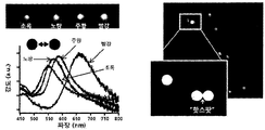
- FIG. 1 illustrates distances between nanoparticles according to colors on a dark field image according to an embodiment of the present invention.
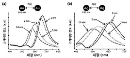
- Figure 2 is a finite-difference time-domain (A) finite-difference time-domain (a) the distance between the gold nanoparticles and (b) the silver nanoparticles according to the color on the dark field image according to an embodiment of the present invention method) is a wavelength-scattered signal intensity spectrum simulated by the method.
- the present invention relates to a method for evaluating a substrate for a SERS sensor, and more particularly, to a method for evaluating the performance of a substrate for a SERS sensor and whether the substrate for a SERS sensor is well manufactured as planned through a simple and systematic method. will be.
- the evaluation method of the substrate for the SERS sensor a) measuring the color of the nanoparticles located on the substrate for the SERS sensor through a dark field microscope; b) converting the measured color into the distance between nanoparticles; c) obtaining the Raman signal strength of the substrate for the SERS sensor; d) obtaining a standard Raman signal intensity of a substrate for a standard SERS sensor comprising nanoparticles having a distance equal to the converted distance; And e) comparing the Raman signal strength with the standard Raman signal strength.
- step c) and step d) may be performed independently of each other in a specific order.
- the substrate for SERS sensor according to the present invention is manufactured by placing the label molecule between the nano thin film and the nanoparticles, which is one of the conventional methods, specifically, a self-assembled monolayer on the nano thin film having a thickness of 10 to 20 nm. After forming a monolayer, nanoparticles having a size of 50 to 100 nm may be dispersed thereon to prepare a substrate for 'surface enhanced Raman scattering' (SERS).
- SERS surface enhanced Raman scattering'
- the substrate according to an example may be used without particular limitation as long as it is commonly used in the art, and specifically, for example, glass, plastic, metal, silicon, quartz or alumina may be used.
- the nano thin film according to an example may be used without particular limitation as long as it is commonly used in the art, for example, a metal nano thin film may be used, and more specifically, for example, gold, silver, copper, titanium, aluminum or Nano thin films, such as platinum, can be used.
- the self-assembled monolayer is preferably used a compound that can bind well to the nano thin film and nanoparticles to amplify the intensity of the surface enhanced Raman scattering, for example -NCS, -NCO, -NH 2 ,- It may be formed using a monomolecular compound having a functional group such as COOH, -NO 2 , -CN or -SH.
- Nanoparticles according to one embodiment may be used without particular limitation as long as the nanoparticles capable of surface enhancement Raman scattering.
- the nanoparticles may be metal nanoparticles, and more specifically, may be gold, silver, platinum, copper, palladium, aluminum, zinc, or a mixture thereof.
- the shape of the nanoparticles may be spherical, rod-shaped, polyhedral or plate-like, and the polyhedron may be hexahedral, octahedral, dodecahedral or icosahedral, but is not limited thereto.
- the average particle diameter of the nanoparticles is not particularly limited as long as it is a size capable of surface enhanced Raman scattering, but may be, for example, 5 to 1,000 nm, more preferably 20 to 200 nm. At this time, if the average particle diameter of the nanoparticles is too small, 5 nm or less, it is not good because the acquisition of Raman signal strength may be difficult.
- the substrate for the SERS sensor can evaluate how well the substrate for the SERS sensor is manufactured by using a simple measuring method.
- the measurement of color may be to measure the color of the plurality of nanoparticles on the substrate for the SERS sensor.
- the color may be measured by the two nanoparticles, or the color may be measured by the nanoparticles within a predetermined region of the substrate for the SERS sensor.
- the predetermined region may mean a partial region or an entire region of the substrate for the SERS sensor.
- the distance between the nanoparticles can be measured using a conventional method, and specifically, for example, a scanning electron microscope (SEM), an atomic force microscope (AFM) or a transmission electron microscope (TEM) a distance between the nanoparticles can be measured using a transmission electron microscope.
- SEM scanning electron microscope
- AFM atomic force microscope
- TEM transmission electron microscope
- FIG. 2 is a wavelength-scattered signal intensity spectrum simulating the relationship between the distance between two metal nanoparticles and the color (scattered color) on a dark field image using the finite-difference time-domain method (FDTD method). It can be seen that the color on the dark field image varies according to the distance between the nanoparticles.
- FIG. 2 is a simulation result, as will be described later, data about colors according to distances between actual nanoparticles may be pre-built to convert distances between particles according to colors measured in a dark field image.
- the dark field image color is red ( ⁇ max 665 to 675 nm).
- the distance between the two nanoparticles may be 1 nm
- the distance between two nanoparticles of red color ( ⁇ max 650-660 nm) may be 2 nm
- the two nanoparticles of orange color ⁇ max 600-610 nm
- the distance between the cells may be 5 nm
- the distance between the two nanoparticles whose color is yellow ( ⁇ max 575 to 585 nm) may be 10 nm.
- two dark field image colors are orange ( ⁇ max 610 to 620 nm).
- the distance between the nanoparticles may be 1 nm
- the distance between two nanoparticles of orange color ( ⁇ max 595-605 nm) may be 2 nm
- the distance between two nanoparticles of green color ⁇ max 530-540 nm
- It may be 5 nm
- the distance between the two nanoparticles of green color ( ⁇ max 500 ⁇ 510 nm) may be 10 nm.
- the light source used for dark field image acquisition may be used without particular limitation as long as it is white light having a wavelength range of 400 to 1000 nm, specifically, for example, tungsten lamp, tungsten-halogen lamp or Xenon (Xe) lamp or the like can be used.
- the measured color can be converted to the distance between the nanoparticles.
- a database that standardizes the distance between particles according to color should be built in advance, and the database must have precision and reliability.
- the color that appears in the actual dark field image, that is, the scattering color may vary according to the variables such as the type and size of the nanoparticles, the shape, and the distance between particles, so that only one variable is different and the others are fixed to be the same. It is necessary to obtain a database for.
- a substrate for a SERS sensor including nanoparticles having a planned type, size, and shape can be prepared, the color can be measured through a dark field microscope, and the distance between particles can be converted according to the measured color. .
- information on the distance between the nanoparticles can be obtained quantitatively through the color shown on the dark field image, and based on this, the distance distribution between the nanoparticles can be known. This information can be effectively used in evaluating the performance and manufacturing state of the substrate for the SERS sensor.
- the conversion to the distance between particles may be a conversion by measuring the color at a single location or by measuring the color at a plurality of locations and then averaged.
- the color may be measured for a plurality of nanoparticles on the substrate for the SERS sensor, and in detail, the color of the two nanoparticles is measured or a predetermined area of the substrate for the SERS sensor. Color may be measured by the nanoparticles in the interior.
- the predetermined region may mean a partial region or an entire region of the substrate for the SERS sensor.
- the color measured by the two nanoparticles can be converted into the distance between the two nanoparticles, or the color measured in the predetermined area of the substrate for the SERS sensor, respectively, converted into distances, and then averaged and averaged. It may be calculated.
- the predetermined region may mean a partial region or an entire region of the substrate for the SERS sensor.
- the Raman signal strength of the SERS sensor substrate and the standard Raman signal strength of the standard SERS sensor substrate can be obtained. As described above, these two steps may be performed independently, and may be performed in no particular order.
- Raman signal strength it can be obtained by using a conventional method, and in detail, it can be measured by irradiating a laser on the manufactured SERS sensor substrate.
- the laser for obtaining the Raman signal strength can be used without particular limitation as long as it is commonly used for Raman spectroscopic measurement, but it is preferable to irradiate laser light energy corresponding to the plasmon resonance energy of the Raman sensor.
- an argon ion laser, a helium-neon laser or a diode laser may be used, but is not limited thereto.
- the Raman signal intensity may be obtained from a single position where color is measured or from the entire surface of the substrate for the SERS sensor.
- the Raman signal intensity may be more effective in evaluating the performance of the SERS sensor substrate or whether the SERS sensor substrate is well manufactured.
- a substrate for a standard SERS sensor may be manufactured by actually irradiating a laser to measure it, or may be obtained using a simulation tool calculated based on quantum mechanical theory.
- the substrate for the standard SERS sensor refers to the substrate for the SERS sensor that has been specified with high reliability such as the type, size, shape and distance between particles of the nanoparticles.
- the substrate for the standard SERS sensor is the SERS sensor designed in the present invention. It may be a standard model of the substrate.
- the standard Raman signal intensity can be obtained using the same method as the method of obtaining the Raman signal intensity.
- the Raman signal strength matches 90% or more of the standard Raman signal strength, it can be evaluated that the Raman sensor is manufactured as planned, and if it is higher than 98%, it can be manufactured with high reliability and high precision. Can be evaluated. On the other hand, if the Raman signal intensity matches less than 90% of the standard Raman signal strength, it can be evaluated that the Raman sensor was not manufactured as planned.
- the manufacturing status and performance of the substrate for the SERS sensor It can be evaluated efficiently.
- such a difference may occur for a variety of reasons, for example, different from the plan, it may be due to the change in the shape of the particles or the arrangement structure between the particles due to the aggregation of nanoparticles.
Landscapes
- Health & Medical Sciences (AREA)
- Physics & Mathematics (AREA)
- General Physics & Mathematics (AREA)
- General Health & Medical Sciences (AREA)
- Chemical & Material Sciences (AREA)
- Immunology (AREA)
- Biochemistry (AREA)
- Analytical Chemistry (AREA)
- Life Sciences & Earth Sciences (AREA)
- Pathology (AREA)
- Nuclear Medicine, Radiotherapy & Molecular Imaging (AREA)
- Spectroscopy & Molecular Physics (AREA)
- Investigating, Analyzing Materials By Fluorescence Or Luminescence (AREA)
- Engineering & Computer Science (AREA)
- Nanotechnology (AREA)
- Radiology & Medical Imaging (AREA)
Abstract
본 발명은 a) 암시야 현미경을 통해 SERS 센서용 기판 상에 위치한 나노입자의 색상을 측정하는 단계; b) 측정된 색상을 나노입자간 거리로 환산하는 단계; c) SERS 센서용 기판의 라만 신호강도를 획득하는 단계; d) 환산된 거리와 동일한 거리를 가지는 나노입자를 포함하는 표준 SERS 센서용 기판의 표준 라만 신호강도를 획득하는 단계; 및 e) 라만 신호강도와 표준 라만 신호강도를 비교하는 단계;를 포함하는 SERS 센서용 기판의 평가방법에 관한 것이다.
Description
본 발명은 SERS 센서용 기판의 평가방법에 관한 것이다.
다양한 형광 표지법을 통한 나노 구조체 및 바이오 시스템의 현상 규명은 표지 부착의 기술적 어려움과 형광 표지에 따른 잘못된 결과 도출 가능성 때문에 물질 자체의 라만 신호 검출을 통한 연구가 대두되고 있다.
그러나 라만 신호 검출은 형광에 비해 매우 작은 신호 크기를 가지기 때문에 실질적 응용에 대한 한계를 가지는 문제점이 있다.
상기의 문제점을 해결하기 위하여 표면 증강 라만 산란(surface enhanced Raman scattering, SERS)을 가능하게 하는 금 또는 은 나노 구조를 이용한 SERS 센서에 대한 연구가 활발히 진행 중에 있다.
이는 나노미터 크기로 제한된 금속 구조 내 플라즈몬, 즉 국소 표면 플라즈몬 공명 (Localized Surface Plasmon Resonance)을 이용한 것으로 금속 나노 구조에 대한 공명 에너지 조사 시 광 신호 증폭으로 극미량 생체 분자 검출과 같은 바이오 센서 응용이 가능할 것이다. 또한 최적의 SERS 센서 구조는 108 이상의 라만 신호 증폭을 가능하게 하여 단일 분자 검출까지 가능하다.
표면 증강 라만 산란신호를 극대화시키기 위하여 다양한 형태의 나노 입자를 합성하거나[Jianping Xie, Jim Yang Lee, and Daniel I. C. Wang, 2007, Chem. Mater., 19, 2823-2830], 나노 입자 사이의 강한 자유 전자의 집단적 진동을 유도[Ping-Ji Huang, et al, 2009, Adv. funct. Mater., 19, 242-248], 자극 반응성 고분자를 사용하여 나노 입자 사이의 거리를 조절[Laura Rodriguez-Lorenzo, et al. 2009, J. AM. CHEM. SOC, 131, 4616-4618]에 대한 기술이 보고되었다. 따라서, 미량의 샘플만으로도 고감도의 바이오센싱 및 화학센싱을 할 수 있는 미량 분석용 SERS 센서용 기판이 고려될 수 있다.
그러나 이와 같은 SERS 센서용 기판이 우수한 성능을 가질 수 있도록 잘 제조되었는가를 평가하는 방법에 대해서는 알려진 바가 없으며, 간단하면서도 체계화된 SERS 센서용 기판의 평가 방법이 필요한 실정이다.
상기와 같은 필요성을 해결하기 위하여 본 발명은 간단하면서도 체계화된 SERS 센서용 기판의 평가방법을 제공하는 것을 목적으로 한다.
상기 목적을 달성하기 위한 본 발명은 a) 암시야 현미경을 통해 SERS 센서용 기판 상에 위치한 나노입자의 색상을 측정하는 단계; b) 측정된 색상을 나노입자간 거리로 환산하는 단계; c) SERS 센서용 기판의 라만 신호강도를 획득하는 단계; d) 환산된 거리와 동일한 거리를 가지는 나노입자를 포함하는 표준 SERS 센서용 기판의 표준 라만 신호강도를 획득하는 단계; 및 e) 라만 신호강도와 표준 라만 신호강도를 비교하는 단계;를 포함하는 SERS 센서용 기판의 평가방법에 관한 것이다.
본 발명에 따른 SERS 센서용 기판의 평가방법은 간단하면서도 체계화된 방법을 통해 SERS 센서용 기판의 성능 및 SERS 센서용 기판이 계획한대로 잘 제조되었는가를 평가할 수 있다.
도 1은 본 발명의 일 예에 따라 암시야 이미지 상의 색상에 따른 나노입자간 거리를 도시화한 것이며,
도 2는 본 발명의 일 예에 따라 암시야 이미지 상의 색상에 따른 (a) 금 나노입자간의 거리 및 (b) 은 나노입자 간의 거리를 유한차분 시간영역법 (FDTD method; finite-difference time-domain method)으로 시뮬레이션한 파장-산란신호강도 스펙트럼이다.
본 발명은 SERS 센서용 기판의 평가방법에 관한 것으로, 보다 상세하게는 간단하면서도 체계화된 방법을 통해, SERS 센서용 기판의 성능 및 SERS 센서용 기판이 계획한대로 잘 제조되었는가를 평가할 수 있는 방법에 관한 것이다.
구체적으로 SERS 센서용 기판의 평가방법은, a) 암시야 현미경을 통해 SERS 센서용 기판 상에 위치한 나노입자의 색상을 측정하는 단계; b) 측정된 색상을 나노입자간 거리로 환산하는 단계; c) SERS 센서용 기판의 라만 신호강도를 획득하는 단계; d) 환산된 거리와 동일한 거리를 가지는 나노입자를 포함하는 표준 SERS 센서용 기판의 표준 라만 신호강도를 획득하는 단계; 및 e) 라만 신호강도와 표준 라만 신호강도를 비교하는 단계;를 포함하여 수행될 수 있다. 이때, c)단계와 d)단계는 각각 독립적인 단계로 특정한 순서 없이 수행될 수 있다.
본 발명에 따른 SERS 센서용 기판은 통상적인 방법 중 하나인 나노 박막과 나노입자 사이에 표지분자를 위치 하게함으로써 제조된 것으로, 구체적으로 10 ~ 20 ㎚ 두께의 나노 박막 위 자기조립단분자층(self-assembled monolayer)을 형성 후 그 위에 50 ~ 100 ㎚ 크기의 나노입자를 분산하여 ‘표면 증강 라만 산란(SERS; surface enhanced Raman scattering)’을 위한 기판을 제조할 수 있다.
이때, 일 예에 따른 기재는 당업계에서 통상적으로 사용되는 것이라면 특별히 제한하지 않고 사용할 수 있으며, 구체적으로 예를 들면, 유리, 플라스틱, 금속, 실리콘, 석영 또는 알루미나 등을 사용할 수 있다.
일 예에 따른 나노 박막은 당업계에서 통상적으로 사용되는 것이라면 특별히 제한하지 않고 사용할 수 있으며, 예를 들면 금속 나노 박막을 사용할 수 있고, 보다 구체적으로 예를 들면 금, 은, 구리, 티타늄, 알루미늄 또는 플래티늄 등의 나노 박막을 사용할 수 있다.
일 예에 따른 자기조립단분자층은 나노 박막 및 나노입자와 잘 결착되어 표면 증강 라만 산란의 세기를 증폭시켜 줄 수 있는 화합물을 사용하는 것이 좋으며, 예를 들어 -NCS, -NCO, -NH2, -COOH, -NO2, -CN 또는 -SH 등의 관능기를 가진 단분자 화합물을 사용하여 형성된 것일 수 있다.
일 예에 따른 나노입자는 표면 증강 라만 산란이 가능한 나노입자라면 특별히 제한하지 않고 사용할 수 있다. 예를 들어 나노입자는 금속 나노입자일 수 있으며, 보다 구체적으로 예를 들면, 금, 은, 백금, 구리, 팔라듐, 알루미늄, 아연 또는 이들의 혼합물 등일 수 있다. 나노입자의 형상은 구형, 막대형, 다면체형 또는 판상형 등일 수 있으며, 다면체형은 육면체형, 팔면체형, 십이면체형 또는 이십면체형 등 일 수 있으나, 이에 한정되진 않는다. 또한, 나노입자의 평균 입경은 표면 증강 라만 산란이 가능한 크기라면 특별히 제한하지 않으나, 예를 들어 5 ~ 1,000 ㎚일 수 있으며, 보다 좋게는 20 ~ 200 ㎚일 수 있다. 이때, 나노입자의 평균 입경이 5 ㎚ 이하로 너무 작으면 라만 신호강도의 획득이 어려울 수 있으므로 좋지 않다.
이와 같이 제조된 SERS 센서용 기판은 간단한 측정방법을 이용하여 SERS 센서용 기판이 얼마나 잘 제조되었는가를 평가할 수 있다.
암시야 현미경을 통해 색상을 측정하는 방법을 보다 자세히 살펴보면,
암시야 현미경(Dark-field microscope)은 특수한 집광렌즈를 사용하여 렌즈의 빗각에서 시료에 빛을 집중시켜 시료에 의해 산란된 빛만 대물렌즈를 통과해 보이도록 하고, 시료를 통과하지 않은 빛은 대물렌즈 속으로 들어가지 않게끔 설계되어 있는 것으로, 본 발명의 경우 SERS 센서용 기판 상에 위치한 나노입자에 의해 산란된 빛만이 대물렌즈를 통과하여 암시야 이미지 상에 색상을 나타나게 되며, 나노입자가 없는 영역은 암시야 이미지 상에 검은색 배경으로 나타나게 된다.
본 발명의 일 예에 따른 색상의 측정은 SERS 센서용 기판 상의 복수개의 나노입자에 대하여 색상을 측정한 것일 수 있다. 상세하게, 두개의 나노입자에 의한 색상을 측정한 것이거나 또는 SERS 센서용 기판의 일정 영역 내의 나노입자에 의한 색상을 측정한 것일 수 있다. 이때 일정 영역이란, SERS 센서용 기판의 일부 영역 또는 전체 영역을 의미하는 것일 수 있다.
암시야 이미지에 나타나는 색상에 대한 일 예로, 두 나노입자가 근거리에 위치할 시, 나노입자간 거리가 가까워짐에 따라 적색이동(red shift)이 일어나 녹색, 노란색, 오렌지색, 붉은색 순으로 장파장의 색상을 나타낼 수 있다. 이때, 나노입자간 거리는 통상적인 방법을 이용하여 측정할 수 있으며, 구체적으로 예를 들면, 주사전자현미경 (SEM; scanning electron microscope), 원자힘현미경(AFM; atomic force microscope) 또는 투과전자현미경(TEM; transmission electron microscope) 등을 통해 나노입자 간의 거리를 측정할 수 있다.
도 2는 두 금속 나노입자 간의 거리와 암시야 이미지 상의 색상(산란색) 간의 관계를 유한차분 시간영역법 (FDTD method; finite-difference time-domain method)으로 시뮬레이션한 파장-산란신호강도 스펙트럼으로, 나노입자 간의 거리에 따라 암시야 이미지 상의 색상이 달라짐을 확인할 수 있다. 도 2는 비록 시뮬레이션 결과이긴 하나, 후술하는 바와 같이, 실제 나노입자 간의 거리에 따른 색상에 대한 데이터를 미리 구축하여 암시야 이미지로 측정된 색상에 따라 입자간 거리를 환산할 수 있다.
구체적으로 예를 들면, 도 2의 (a)에 나타난 바와 같이, 입경이 100 ㎚인 구형의 두 금(Au) 나노입자의 경우, 암시야 이미지 색상이 붉은색 (λmax 665~675 ㎚)인 두 나노입자간의 거리는 1 ㎚일 수 있으며, 색상이 붉은색(λmax 650~660 ㎚)인 두 나노입자간의 거리는 2 ㎚일 수 있으며, 색상이 오렌지색(λmax 600~610 ㎚)인 두 나노입자간의 거리는 5 ㎚일 수 있으며, 색상이 노란색(λmax 575~585 ㎚)인 두 나노입자간의 거리는 10 ㎚일 수 있다.
다른 일 구체예로, 도 2의 (b)에 나타난 바와 같이, 입경이 100 ㎚인 구형의 두 은(Ag) 나노입자의 경우, 암시야 이미지 색상이 오렌지색 (λmax 610~620 ㎚)인 두 나노입자간의 거리는 1 ㎚일 수 있으며, 색상이 오렌지색(λmax 595~605 ㎚)인 두 나노입자간의 거리는 2 ㎚일 수 있으며, 색상이 녹색(λmax 530~540 ㎚)인 두 나노입자간의 거리는 5 ㎚일 수 있으며, 색상이 녹색(λmax 500~510 ㎚)인 두 나노입자간의 거리는 10 ㎚일 수 있다.
본 발명의 일 예에 있어, 암시야 이미지 획득을 위해 사용되는 광원은 400 ~ 1000 ㎚ 파장영역을 갖는 백색광이라면 특별히 제한하지 않고 사용할 수 있으며, 구체적으로 예를 들면, 텅스텐 램프, 텅스텐-할로겐 램프 또는 크세논(Xe) 램프 등을 사용할 수 있다.
색상의 측정이 완료되면, 측정된 색상을 나노입자간 거리로 환산할 수 있다. 단, 본 단계를 수행하기에 앞서, 색상에 따른 입자간 거리를 표준화한 데이터베이스가 미리 구축되어 있어야 하며, 데이터베이스는 정밀도 및 신뢰도가 있어야 한다. 실제 암시야 이미지 상에 나타나는 색상, 즉 산란색은 나노입자의 종류와 크기, 형상 그리고 입자간 거리 등과 같은 변수에 따라 달라질 수 있으므로, 하나의 변수만을 달리하고 나머지는 동일하게 고정하여 되도록 많은 경우에 대한 데이터베이스를 획득하는 것이 필요하다. 데이터베이스가 구축되면, 계획된 종류, 크기 및 형상을 가지는 나노입자를 포함하는 SERS 센서용 기판을 제조하고 이를 암시야 현미경을 통해 색상을 측정한 후, 측정된 색상에 따라 입자간 거리를 환산할 수 있다.
이에 따라, 암시야 이미지 상에 나타난 색상을 통해 나노입자 간의 거리에 대한 정보를 정량적으로 수득할 수 있으며, 이를 바탕으로 나노입자간 거리 분포 등을 알 수 있다. 이러한 정보는 SERS 센서용 기판의 성능 및 제조 상태를 평가함에 있어 유효하게 사용될 수 있다.
본 발명의 일 예에 따른 입자간 거리로의 환산은 단일 위치에서 색상을 측정하여 환산한 것이거나 또는 복수의 위치에서 색상을 측정한 후 환산하여 평균을 낸 것일 수 있다.
앞서 색상 측정에서 설명한 바와 같이, 색상은 SERS 센서용 기판 상의 복수개의 나노입자에 대하여 측정된 것일 수 있으며, 상세하게는 두개의 나노입자에 의한 색상을 측정한 것이거나 또는 SERS 센서용 기판의 일정 영역 내의 나노입자에 의한 색상을 측정한 것일 수 있다. 이때 일정 영역이란, SERS 센서용 기판의 일부 영역 또는 전체 영역을 의미하는 것일 수 있다.
이에 따라, 두개의 나노입자에 의해 측정된 색상을 통하여 두 나노입자 간의 거리로 환산할 수 있으며, 또는 SERS 센서용 기판의 일정 영역 내에서 측정된 색상들을 각각 거리로 환산한 후 이를 평균 내어 평균 거리를 계산한 것일 수 있다. 앞서 설명한 바와 같이 이때 일정 영역이란 SERS 센서용 기판의 일부 영역 또는 전체 영역을 의미하는 것일 수 있다.
다음으로, SERS 센서용 기판의 라만 신호강도 및 표준 SERS 센서용 기판의 표준 라만 신호강도를 획득할 수 있다. 앞서 설명한 바와 같이 이 두 단계는 각각 독립적으로 수행되는 것으로 특정 순서 없이 이루어질 수 있다.
라만 신호강도의 경우, 통상적인 방법을 이용하여 획득할 수 있으며, 상세하게는 제조한 SERS 센서용 기판에 레이저를 조사하여 측정할 수 있다. 라만 신호강도의 획득을 위한 레이저는 라만 분광 측정을 위해 통상적으로 사용되는 것이라면 특별히 제한하지 않고 사용할 수 있으나, 라만센서의 플라즈몬 공명에너지에 준하는 레이저 광 에너지를 조사하는 것이 바람직하다. 구체적으로 예를 들면 아르곤이온 레이저, 헬륨-네온 레이저 또는 다이오드 레이저 등을 사용할 수 있으나, 이에 한정되는 것은 아니다.
이때, 라만 신호강도는 색상이 측정된 단일 위치에서 획득한 것이거나 또는 SERS 센서용 기판 전체 표면에서 획득한 것일 수 있다. 특히, SERS 센서용 기판 전체 표면에서 라만 신호강도를 획득한 경우, SERS 센서용 기판의 성능 또는 SERS 센서용 기판이 잘 제조되었는가를 평가함에 있어서 보다 효과적일 수 있다.
표준 라만 신호강도의 경우, 표준 SERS 센서용 기판을 실 제조하여 레이저를 조사하여 측정하거나, 양자역학적 이론을 기반으로 하여 계산되는 시뮬레이션 툴을 이용하여 얻어질 수 있다.
여기서 표준 SERS 센서용 기판이란, 나노입자의 종류와 크기, 형상 그리고 입자간 거리 등과 같은 변수가 높은 신뢰성으로 특정 지어진 SERS 센서용 기판을 일컫는 것으로, 표준 SERS 센서용 기판은 본 발명에서 설계한 SERS 센서용 기판의 표준 모델일 수 있다.
실 제조한 표준 SERS 센서용 기판에 레이저를 조사하여 표준 라만 신호강도를 수득하고자 하는 경우, 라만 신호강도를 획득한 방법과 동일한 방법을 이용하여 표준 라만 신호강도를 획득할 수 있다.
다음으로, 각각 획득한 라만 신호강도와 표준 라만 신호강도를 비교하여 SERS 센서용 기판을 평가할 수 있다.
예를 들어, 라만 신호강도가 표준 라만신호강도와 90% 이상으로 일치할 경우, 라만센서가 계획한 바대로 잘 제조되었다고 평가할 수 있으며, 98% 이상으로 일치할 경우, 높은 신뢰성으로 매우 정밀하게 제조되었다고 평가할 수 있다. 반면, 라만 신호강도가 표준 라만신호강도가 90% 미만으로 일치할 경우, 라만센서가 계획한 바대로 제조되지 않았다고 평가할 수 있다.
또한, 라만 신호강도와 표준 라만 신호강도를 비교함과 더불어, 앞서 설명한 바와 같이, 암시야 이미지를 통해 획득한 나노입자간 거리 분포 등의 정보를 바탕으로 SERS 센서용 기판의 제조 상태 및 성능을 보다 효율적으로 평가할 수 있다.
한편, 이러한 차이가 발생하는 것은 다양한 이유가 있을 수 있으며, 예를 들어, 계획한 바와는 달리, 나노입자의 뭉침에 의해 입자의 형상이 달라지거나 입자간의 배열 구조가 달라짐 등으로 인한 것일 수 있다.
본 발명에 있어서 달리 정의되지 않은 한, 모든 기술적 용어 및 과학적 용어는 본 발명이 속하는 당업자 중 하나에 의해 일반적으로 이해되는 의미와 동일한 의미를 갖는다. 본원에서 설명에 사용되는 용어는 단지 특정 실시예를 효과적으로 기술하기 위함이고 본 발명을 제한하는 것으로 의도되지 않는다.
또한 다음에 소개되는 도면들은 당업자에게 본 발명의 사상이 충분히 전달될 수 있도록 하기 위해 예로서 제공되는 것이다. 따라서 본 발명은 이하 제시되는 도면들에 한정되지 않고 다른 형태로 구체화될 수도 있으며, 이하 제시되는 도면들은 본 발명의 사상을 명확히 하기 위해 과장되어 도시될 수 있다.
또한 명세서 및 첨부된 특허청구범위에서 사용되는 단수 형태는 문맥에서 특별한 지시가 없는 한 복수 형태도 포함하는 것으로 의도할 수 있다.
Claims (9)
- a) 암시야 현미경을 통해 SERS 센서용 기판 상에 위치한 나노입자의 색상을 측정하는 단계;b) 상기 측정된 색상을 나노입자간 거리로 환산하는 단계;c) 상기 SERS 센서용 기판의 라만 신호강도를 획득하는 단계;d) 상기 환산된 거리와 동일한 거리를 가지는 나노입자를 포함하는 표준 SERS 센서용 기판의 표준 라만 신호강도를 획득하는 단계; 및e) 상기 라만 신호강도와 상기 표준 라만 신호강도를 비교하는 단계;를 포함하는 SERS 센서용 기판의 평가방법.
- 제 1항에 있어서,상기 나노입자는 금속 나노입자인 것을 특징으로 하는 SERS 센서용 기판의 평가방법.
- 제 2항에 있어서,상기 금속 나노입자는 금, 은, 백금, 구리, 팔라듐, 알루미늄, 아연 또는 이들의 혼합물인 SERS 센서용 기판의 평가방법.
- 제 1항에 있어서,상기 나노입자의 평균 입경은 5 ~ 1,000 ㎚인 SERS 센서용 기판의 평가방법.
- 제 1항에 있어서,상기 c)단계의 라만 신호강도는 레이저를 조사하여 획득하는 SERS 센서용 기판의 평가방법.
- 제 5항에 있어서,상기 레이저는 아르곤 이온 레이저, 헬륨-네온 레이저 또는 다이오드 레이저인 SERS 센서용 기판의 평가방법.
- 제 1항에 있어서,상기 c)단계의 라만 신호강도는 색상이 측정된 단일 위치에서 획득된 것을 특징으로 하는 SERS 센서용 기판의 평가방법.
- 제 1항에 있어서,상기 c)단계의 라만 신호강도는 SERS 센서용 기판의 전체 표면에서 획득된 것을 특징으로 하는 SERS 센서용 기판의 평가방법.
- 제 1항에 있어서,상기 b)단계는 복수의 위치에서 색상을 측정한 후 환산하여 평균한 것을 특징으로 하는 SERS 센서용 기판의 평가방법.
Priority Applications (1)
| Application Number | Priority Date | Filing Date | Title |
|---|---|---|---|
| US15/580,117 US10082468B2 (en) | 2016-04-27 | 2017-04-27 | Method for evaluating SERS sensor substrate |
Applications Claiming Priority (2)
| Application Number | Priority Date | Filing Date | Title |
|---|---|---|---|
| KR1020160051363A KR101706064B1 (ko) | 2016-04-27 | 2016-04-27 | 라만측정용 기판의 평가방법 |
| KR10-2016-0051363 | 2016-04-27 |
Publications (1)
| Publication Number | Publication Date |
|---|---|
| WO2017188744A1 true WO2017188744A1 (ko) | 2017-11-02 |
Family
ID=58111745
Family Applications (1)
| Application Number | Title | Priority Date | Filing Date |
|---|---|---|---|
| PCT/KR2017/004474 Ceased WO2017188744A1 (ko) | 2016-04-27 | 2017-04-27 | Sers 센서용 기판의 평가방법 |
Country Status (3)
| Country | Link |
|---|---|
| US (1) | US10082468B2 (ko) |
| KR (1) | KR101706064B1 (ko) |
| WO (1) | WO2017188744A1 (ko) |
Families Citing this family (2)
| Publication number | Priority date | Publication date | Assignee | Title |
|---|---|---|---|---|
| TWI912371B (zh) * | 2021-01-14 | 2026-01-21 | 瑞士商通用表面增強光譜學股份有限公司 | 用於判定顆粒尺寸之方法及用於該方法之總成 |
| WO2022221191A1 (en) * | 2021-04-16 | 2022-10-20 | The Johns Hopkins University | Surface enhanced raman spectroscopy method of pathogen detection and substrate for the same |
Citations (5)
| Publication number | Priority date | Publication date | Assignee | Title |
|---|---|---|---|---|
| KR20110047921A (ko) * | 2009-10-31 | 2011-05-09 | 숭실대학교산학협력단 | 금 나노콜로이드 입자를 이용한 수용액내의 Hg(Ⅱ)농도의 형광 및 SERS 탐지방법 |
| KR20120134910A (ko) * | 2011-06-03 | 2012-12-12 | 한국과학기술원 | 나노 물질의 광학적 특성을 이용한 변형률 측정 방법 및 장치 |
| KR101448111B1 (ko) * | 2013-09-17 | 2014-10-13 | 한국기계연구원 | 표면 증강 라만 분광용 기판 및 이의 제조방법 |
| KR20150000751A (ko) * | 2013-06-25 | 2015-01-05 | 국방과학연구소 | 미량 분석용 고감도 자극 반응성 표면증강 라만 산란 기판 제조 방법 및 그의 응용 |
| KR20160038205A (ko) * | 2014-09-29 | 2016-04-07 | 한국기계연구원 | 나노갭이 조절된 기판 및 이의 제조방법 |
Family Cites Families (1)
| Publication number | Priority date | Publication date | Assignee | Title |
|---|---|---|---|---|
| US20100053598A1 (en) * | 2008-08-27 | 2010-03-04 | Sunghoon Kwon | Surface deformation detection |
-
2016
- 2016-04-27 KR KR1020160051363A patent/KR101706064B1/ko active Active
-
2017
- 2017-04-27 WO PCT/KR2017/004474 patent/WO2017188744A1/ko not_active Ceased
- 2017-04-27 US US15/580,117 patent/US10082468B2/en active Active
Patent Citations (5)
| Publication number | Priority date | Publication date | Assignee | Title |
|---|---|---|---|---|
| KR20110047921A (ko) * | 2009-10-31 | 2011-05-09 | 숭실대학교산학협력단 | 금 나노콜로이드 입자를 이용한 수용액내의 Hg(Ⅱ)농도의 형광 및 SERS 탐지방법 |
| KR20120134910A (ko) * | 2011-06-03 | 2012-12-12 | 한국과학기술원 | 나노 물질의 광학적 특성을 이용한 변형률 측정 방법 및 장치 |
| KR20150000751A (ko) * | 2013-06-25 | 2015-01-05 | 국방과학연구소 | 미량 분석용 고감도 자극 반응성 표면증강 라만 산란 기판 제조 방법 및 그의 응용 |
| KR101448111B1 (ko) * | 2013-09-17 | 2014-10-13 | 한국기계연구원 | 표면 증강 라만 분광용 기판 및 이의 제조방법 |
| KR20160038205A (ko) * | 2014-09-29 | 2016-04-07 | 한국기계연구원 | 나노갭이 조절된 기판 및 이의 제조방법 |
Also Published As
| Publication number | Publication date |
|---|---|
| KR101706064B1 (ko) | 2017-02-15 |
| US10082468B2 (en) | 2018-09-25 |
| US20180136136A1 (en) | 2018-05-17 |
Similar Documents
| Publication | Publication Date | Title |
|---|---|---|
| Hong et al. | Nanobiosensors based on localized surface plasmon resonance for biomarker detection | |
| AU2004308238B2 (en) | Surface enhanced raman spectroscopy (SERS)-active composite nanoparticles methods of fabrication thereof and methods of use thereof | |
| Cialla et al. | Surface-enhanced Raman spectroscopy (SERS): progress and trends | |
| Li et al. | Analytical methods based on the light-scattering of plasmonic nanoparticles at the single particle level with dark-field microscopy imaging | |
| US20130242297A1 (en) | Substrate for optical sensing by surface enhanced raman spectroscopy (sers) and methods for forming the same | |
| Liu et al. | Increasing hotspots density for high-sensitivity SERS detection by assembling array of Ag nanocubes | |
| CN107132212B (zh) | 一种表面增强拉曼散射传感器件的制备方法 | |
| Wu et al. | Highly sensitive label-free detection of analytes at different scales using uniform graphene-nanopyramids hybrid SERS system | |
| Jensen et al. | Single nanoparticle based optical pH probe | |
| Zhang et al. | Localized photonic nanojet based sensing platform for highly efficient signal amplification and quantitative biosensing | |
| Meng et al. | Optical fiber optrodes with silver-coated gold nanocavity ordered arrays for highly sensitive surface enhanced Raman spectrum | |
| Yang et al. | Ultrasensitive multiplex SERS immunoassay based on porous Au–Ag alloy nanoparticle–amplified Raman signal probe and encoded photonic crystal beads | |
| Fan et al. | Three-dimensional SERS sensor based on the sandwiched G@ AgNPs@ G/PDMS film | |
| Tan et al. | Stretchable and flexible micro–nano substrates for SERS detection of organic dyes | |
| Cui et al. | Nanopillar array-based plasmonic metasurface for switchable multifunctional biosensing | |
| WO2017188744A1 (ko) | Sers 센서용 기판의 평가방법 | |
| CN106033086B (zh) | 基于lspr检测精子顶体酶活性的方法、试剂盒及其应用 | |
| WO2016093569A1 (ko) | 플라즈모닉 종이 및 이의 제조 방법 | |
| JP2019203818A (ja) | センシング用チップ、センシング用キット及びそれを用いたセンシング方法 | |
| Ke et al. | Enhancing the Sensitivity of Ag/ZnO NRs SERS Substrates to Fast Green Dyes by the Assistance of Centrifuged Ag Nanoparticles | |
| Xia et al. | Templated gold nanocaps for surface-enhanced Raman scattering (SERS) sensors based on monolayer polystyrene colloidal arrays | |
| Polley et al. | Plasmonic Lab-on-fiber Sensor: Fabrication and Subsequent Optimization | |
| CN115876747B (zh) | 金纳米空心圆台阵列表面增强拉曼散射基底及检测方法 | |
| Capelo et al. | based luminescent filters for smart detection of nanomaterials in workplace exposure assessments | |
| Mehta et al. | Novel low-cost periodic and flexible SERS substrate fabrication via soft lithography and glancing angle deposition technique |
Legal Events
| Date | Code | Title | Description |
|---|---|---|---|
| WWE | Wipo information: entry into national phase |
Ref document number: 15580117 Country of ref document: US |
|
| NENP | Non-entry into the national phase |
Ref country code: DE |
|
| 121 | Ep: the epo has been informed by wipo that ep was designated in this application |
Ref document number: 17789928 Country of ref document: EP Kind code of ref document: A1 |
|
| 122 | Ep: pct application non-entry in european phase |
Ref document number: 17789928 Country of ref document: EP Kind code of ref document: A1 |