WO2017183692A1 - Light control film, laminated glass and method for producing light control film - Google Patents
Light control film, laminated glass and method for producing light control film Download PDFInfo
- Publication number
- WO2017183692A1 WO2017183692A1 PCT/JP2017/015895 JP2017015895W WO2017183692A1 WO 2017183692 A1 WO2017183692 A1 WO 2017183692A1 JP 2017015895 W JP2017015895 W JP 2017015895W WO 2017183692 A1 WO2017183692 A1 WO 2017183692A1
- Authority
- WO
- WIPO (PCT)
- Prior art keywords
- spacer
- laminate
- liquid crystal
- light control
- control film
- Prior art date
Links
Images


Classifications
-
- G—PHYSICS
- G02—OPTICS
- G02F—OPTICAL DEVICES OR ARRANGEMENTS FOR THE CONTROL OF LIGHT BY MODIFICATION OF THE OPTICAL PROPERTIES OF THE MEDIA OF THE ELEMENTS INVOLVED THEREIN; NON-LINEAR OPTICS; FREQUENCY-CHANGING OF LIGHT; OPTICAL LOGIC ELEMENTS; OPTICAL ANALOGUE/DIGITAL CONVERTERS
- G02F1/00—Devices or arrangements for the control of the intensity, colour, phase, polarisation or direction of light arriving from an independent light source, e.g. switching, gating or modulating; Non-linear optics
- G02F1/01—Devices or arrangements for the control of the intensity, colour, phase, polarisation or direction of light arriving from an independent light source, e.g. switching, gating or modulating; Non-linear optics for the control of the intensity, phase, polarisation or colour
- G02F1/13—Devices or arrangements for the control of the intensity, colour, phase, polarisation or direction of light arriving from an independent light source, e.g. switching, gating or modulating; Non-linear optics for the control of the intensity, phase, polarisation or colour based on liquid crystals, e.g. single liquid crystal display cells
- G02F1/133—Constructional arrangements; Operation of liquid crystal cells; Circuit arrangements
- G02F1/1333—Constructional arrangements; Manufacturing methods
- G02F1/1339—Gaskets; Spacers; Sealing of cells
- G02F1/13394—Gaskets; Spacers; Sealing of cells spacers regularly patterned on the cell subtrate, e.g. walls, pillars
-
- E—FIXED CONSTRUCTIONS
- E06—DOORS, WINDOWS, SHUTTERS, OR ROLLER BLINDS IN GENERAL; LADDERS
- E06B—FIXED OR MOVABLE CLOSURES FOR OPENINGS IN BUILDINGS, VEHICLES, FENCES OR LIKE ENCLOSURES IN GENERAL, e.g. DOORS, WINDOWS, BLINDS, GATES
- E06B3/00—Window sashes, door leaves, or like elements for closing wall or like openings; Layout of fixed or moving closures, e.g. windows in wall or like openings; Features of rigidly-mounted outer frames relating to the mounting of wing frames
- E06B3/66—Units comprising two or more parallel glass or like panes permanently secured together
-
- E—FIXED CONSTRUCTIONS
- E06—DOORS, WINDOWS, SHUTTERS, OR ROLLER BLINDS IN GENERAL; LADDERS
- E06B—FIXED OR MOVABLE CLOSURES FOR OPENINGS IN BUILDINGS, VEHICLES, FENCES OR LIKE ENCLOSURES IN GENERAL, e.g. DOORS, WINDOWS, BLINDS, GATES
- E06B9/00—Screening or protective devices for wall or similar openings, with or without operating or securing mechanisms; Closures of similar construction
- E06B9/24—Screens or other constructions affording protection against light, especially against sunshine; Similar screens for privacy or appearance; Slat blinds
-
- G—PHYSICS
- G02—OPTICS
- G02F—OPTICAL DEVICES OR ARRANGEMENTS FOR THE CONTROL OF LIGHT BY MODIFICATION OF THE OPTICAL PROPERTIES OF THE MEDIA OF THE ELEMENTS INVOLVED THEREIN; NON-LINEAR OPTICS; FREQUENCY-CHANGING OF LIGHT; OPTICAL LOGIC ELEMENTS; OPTICAL ANALOGUE/DIGITAL CONVERTERS
- G02F1/00—Devices or arrangements for the control of the intensity, colour, phase, polarisation or direction of light arriving from an independent light source, e.g. switching, gating or modulating; Non-linear optics
- G02F1/01—Devices or arrangements for the control of the intensity, colour, phase, polarisation or direction of light arriving from an independent light source, e.g. switching, gating or modulating; Non-linear optics for the control of the intensity, phase, polarisation or colour
- G02F1/13—Devices or arrangements for the control of the intensity, colour, phase, polarisation or direction of light arriving from an independent light source, e.g. switching, gating or modulating; Non-linear optics for the control of the intensity, phase, polarisation or colour based on liquid crystals, e.g. single liquid crystal display cells
- G02F1/133—Constructional arrangements; Operation of liquid crystal cells; Circuit arrangements
- G02F1/1333—Constructional arrangements; Manufacturing methods
- G02F1/1339—Gaskets; Spacers; Sealing of cells
- G02F1/13392—Gaskets; Spacers; Sealing of cells spacers dispersed on the cell substrate, e.g. spherical particles, microfibres
-
- G—PHYSICS
- G02—OPTICS
- G02F—OPTICAL DEVICES OR ARRANGEMENTS FOR THE CONTROL OF LIGHT BY MODIFICATION OF THE OPTICAL PROPERTIES OF THE MEDIA OF THE ELEMENTS INVOLVED THEREIN; NON-LINEAR OPTICS; FREQUENCY-CHANGING OF LIGHT; OPTICAL LOGIC ELEMENTS; OPTICAL ANALOGUE/DIGITAL CONVERTERS
- G02F1/00—Devices or arrangements for the control of the intensity, colour, phase, polarisation or direction of light arriving from an independent light source, e.g. switching, gating or modulating; Non-linear optics
- G02F1/01—Devices or arrangements for the control of the intensity, colour, phase, polarisation or direction of light arriving from an independent light source, e.g. switching, gating or modulating; Non-linear optics for the control of the intensity, phase, polarisation or colour
- G02F1/13—Devices or arrangements for the control of the intensity, colour, phase, polarisation or direction of light arriving from an independent light source, e.g. switching, gating or modulating; Non-linear optics for the control of the intensity, phase, polarisation or colour based on liquid crystals, e.g. single liquid crystal display cells
- G02F1/133—Constructional arrangements; Operation of liquid crystal cells; Circuit arrangements
- G02F1/1333—Constructional arrangements; Manufacturing methods
- G02F1/1337—Surface-induced orientation of the liquid crystal molecules, e.g. by alignment layers
-
- G—PHYSICS
- G02—OPTICS
- G02F—OPTICAL DEVICES OR ARRANGEMENTS FOR THE CONTROL OF LIGHT BY MODIFICATION OF THE OPTICAL PROPERTIES OF THE MEDIA OF THE ELEMENTS INVOLVED THEREIN; NON-LINEAR OPTICS; FREQUENCY-CHANGING OF LIGHT; OPTICAL LOGIC ELEMENTS; OPTICAL ANALOGUE/DIGITAL CONVERTERS
- G02F1/00—Devices or arrangements for the control of the intensity, colour, phase, polarisation or direction of light arriving from an independent light source, e.g. switching, gating or modulating; Non-linear optics
- G02F1/01—Devices or arrangements for the control of the intensity, colour, phase, polarisation or direction of light arriving from an independent light source, e.g. switching, gating or modulating; Non-linear optics for the control of the intensity, phase, polarisation or colour
- G02F1/13—Devices or arrangements for the control of the intensity, colour, phase, polarisation or direction of light arriving from an independent light source, e.g. switching, gating or modulating; Non-linear optics for the control of the intensity, phase, polarisation or colour based on liquid crystals, e.g. single liquid crystal display cells
- G02F1/133—Constructional arrangements; Operation of liquid crystal cells; Circuit arrangements
- G02F1/1333—Constructional arrangements; Manufacturing methods
- G02F1/1339—Gaskets; Spacers; Sealing of cells
- G02F1/13398—Spacer materials; Spacer properties
-
- G—PHYSICS
- G02—OPTICS
- G02F—OPTICAL DEVICES OR ARRANGEMENTS FOR THE CONTROL OF LIGHT BY MODIFICATION OF THE OPTICAL PROPERTIES OF THE MEDIA OF THE ELEMENTS INVOLVED THEREIN; NON-LINEAR OPTICS; FREQUENCY-CHANGING OF LIGHT; OPTICAL LOGIC ELEMENTS; OPTICAL ANALOGUE/DIGITAL CONVERTERS
- G02F1/00—Devices or arrangements for the control of the intensity, colour, phase, polarisation or direction of light arriving from an independent light source, e.g. switching, gating or modulating; Non-linear optics
- G02F1/01—Devices or arrangements for the control of the intensity, colour, phase, polarisation or direction of light arriving from an independent light source, e.g. switching, gating or modulating; Non-linear optics for the control of the intensity, phase, polarisation or colour
- G02F1/13—Devices or arrangements for the control of the intensity, colour, phase, polarisation or direction of light arriving from an independent light source, e.g. switching, gating or modulating; Non-linear optics for the control of the intensity, phase, polarisation or colour based on liquid crystals, e.g. single liquid crystal display cells
- G02F1/133—Constructional arrangements; Operation of liquid crystal cells; Circuit arrangements
- G02F1/1333—Constructional arrangements; Manufacturing methods
- G02F1/1343—Electrodes
- G02F1/134309—Electrodes characterised by their geometrical arrangement
- G02F1/134363—Electrodes characterised by their geometrical arrangement for applying an electric field parallel to the substrate, i.e. in-plane switching [IPS]
Definitions
- the present invention relates to a light control film that can be used in, for example, an electronic blind that is attached to a window to control the transmission of extraneous light, and a laminated glass using this light control film.
- Patent Documents 1 and 2 various devices relating to a light control film that can be used for, for example, an electronic blind that is attached to a window to control the transmission of extraneous light have been proposed (Patent Documents 1 and 2).
- One such light control film uses liquid crystal.
- the light control film using the liquid crystal is manufactured by sandwiching a liquid crystal material with a transparent plate material on which a transparent electrode is manufactured, and manufacturing the liquid crystal cell with a linear polarizing plate.
- this light control film changes the orientation of the liquid crystal by changing the electric field applied to the liquid crystal to block or transmit the extraneous light, and further changes the amount of transmitted light. To control.
- Such a light control film is configured such that a spacer is provided on a transparent substrate constituting the liquid crystal cell, and the liquid crystal layer is held at a constant thickness by the spacer.
- the spacer has a configuration widely used in image display panels, and is manufactured in a column shape using, for example, a photoresist. Further, for example, a bead spacer can be applied. Patent Documents 3 and 4 propose a device for this bead spacer.
- the spacer may be crushed or the tip of the spacer may penetrate into the opposite surface due to the pressing force during use.
- the conventional light control film may have a nonuniform cell gap or a local alignment failure, which may make it difficult to perform uniform light control.
- the liquid crystal material leaked out.
- the conventional light control film still has a practically insufficient problem with respect to the reliability of the spacer.
- JP 03-47392 A Japanese Patent Laid-Open No. 08-184273 JP-A-62-286023 Japanese Patent Laid-Open No. 02-120719
- This invention is made in view of such a situation, and it aims at enabling it to improve the reliability regarding a spacer further compared with the former.
- the present inventor has intensively studied to solve the above-mentioned problems, and has come up with the idea that the Vickers hardness value Xs of the spacer and the Vickers hardness value Xf of the surface with which the spacer tip abuts are selected, respectively. It came to be completed.
- the present inventor has conducted extensive research to solve the above-mentioned problems, and the Vickers hardness value B of the surface where the bead spacer abuts, the occupation ratio A and the hardness which are the ratio of the area occupied by the bead spacer in a plan view. The idea of selecting a multiplication value A ⁇ B with the value B was reached, and the present invention was completed.
- the present invention provides the following.
- a liquid crystal layer is sandwiched between first and second laminated bodies each including at least an alignment layer, and liquid crystal molecules related to the liquid crystal layer are driven by driving electrodes provided in the first and second laminated bodies.
- the light control film that controls the transmitted light by controlling the orientation of The first laminate is A spacer that holds the thickness of the liquid crystal layer is provided on the substrate made of a transparent film material, The first and second laminates are: The Vickers hardness value Xs of the spacer is 16.9 or more and 40.2 or less, and the Vickers hardness value Xf of the portion of the second laminated body with which the tip of the spacer contacts is 11.8 or more and 35.9 or less.
- a light control film is 16.9 or more and 40.2 or less.
- the Vickers hardness value Xs of the spacer is 16.9 or more and 40.2 or less
- the Vickers hardness value Xf of the portion of the second laminated body with which the tip of the spacer abuts is 11.8 or more and 35. .9 or less
- the Vickers hardness value Xf of the portion of the second laminated body with which the tip of the spacer abuts is 11.8 or more and 35. .9 or less
- leakage of the liquid crystal material can be effectively avoided.
- a liquid crystal layer is sandwiched between first and second laminated bodies each including at least an alignment layer, and liquid crystal molecules related to the liquid crystal layer are driven by driving electrodes provided in the first and second laminated bodies.
- a base material made of a transparent film material is provided with a bead spacer for maintaining the thickness of the liquid crystal layer,
- the first and second laminates are:
- the Vickers hardness value B of the portion of the second laminate in contact with the bead spacer is 11.8 or more and 35.9 or less
- a multiplication value A ⁇ B of an occupation ratio A which is a ratio of an area occupied by the bead spacer on the first laminate and the Vickers hardness value B is:
- the light control film which is 0.42 or more.
- the Vickers hardness value B when the Vickers hardness value B is 11.8 or more and 35.9 or less, it is possible to reduce the situation where the bead spacer penetrates the opposing surface due to the pressing force during use, etc. It is possible to reduce cell gap nonuniformity and local alignment failure, and to effectively avoid leakage of liquid crystal material. Further, it is possible to reduce the damage to the base material and to reduce the occurrence of cracks when the whole is bent.
- the multiplication value A ⁇ B of the occupation ratio A and the Vickers hardness value B is 0.42 or more, when the occupation ratio A is small, the Vickers hardness value B is set to be large, and the bead spacer The cell gap can be maintained by the hardness value B corresponding to the stress concentration on the surface, and the reliability of the bead spacer can be further improved as compared with the conventional case.
- the laminated glass can be constituted by the light control film which is further improved in reliability with respect to the spacer as compared with the related art.
- the first laminate manufacturing process includes: The substrate includes a spacer manufacturing process for manufacturing a spacer that maintains the thickness of the liquid crystal layer, The spacer manufacturing process includes The spacer is manufactured so that the Vickers hardness value Xs of the spacer is 16.9 or more and 40.2 or less,
- the second laminate manufacturing process includes: A method for producing a light control film, wherein the second laminate is produced such that a Vickers hardness value Xf of a portion of the second laminate in contact with a tip of the spacer is 11.8 or more and 35.9 or less.
- the Vickers hardness value Xs of the spacer is 16.9 or more and 40.2 or less
- the Vickers hardness value Xf of the portion of the second laminated body with which the tip of the spacer contacts is 11.8 or more and 35. .9 or less reduces the situation in which the tip of the spacer penetrates into the opposite surface due to the pressing force during use, etc., reducing the occurrence of nonuniform cell gaps and local alignment failure
- leakage of the liquid crystal material can be effectively avoided.
- the first laminate manufacturing process includes: The substrate comprises a bead spacer arrangement step of arranging a bead spacer for maintaining the thickness of the liquid crystal layer,
- the second laminate manufacturing process includes: Producing the second laminate so that the Vickers hardness value B of the portion of the second laminate in contact with the bead spacer is 11.8 or more and 35.9 or less,
- the bead spacer arranging step includes In a state where the first laminate is viewed in plan, a multiplication value A ⁇ B of an occupation ratio A which is a ratio of an area occupied by the bead spacer on the first laminate and the Vickers hardness value B is:
- the manufacturing method of the light control film which arrange
- the Vickers hardness value B when the Vickers hardness value B is 11.8 or more and 35.9 or less, the situation in which the bead spacer penetrates into the opposing surface due to the pressing force during use, etc. is reduced. It is possible to reduce cell gap nonuniformity and local alignment failure, and to effectively avoid leakage of liquid crystal material.
- the multiplication value A ⁇ B of the occupation ratio A and the Vickers hardness value B is 0.42 or more, when the occupation ratio A is small, the Vickers hardness value B is set to be large, and the bead spacer The cell gap can be held by the hardness value B corresponding to the stress concentration on the surface, thereby reducing the situation in which the bead spacer penetrates into the surface that is further opposed to the cell gap. Alignment defects can be reduced, and leakage of the liquid crystal material can be effectively avoided. By these, the reliability regarding a bead spacer can be improved further compared with the past.
- the reliability related to the spacer can be further improved as compared with the conventional case.
- FIG. 1 is a cross-sectional view showing a laminated glass according to the first embodiment of the present invention.
- the laminated glass 1 is a laminated glass applied to, for example, a vehicle window, and is configured by sandwiching a light control film 10 between plate glasses 2 and 3 through intermediate layers 4 and 5, respectively.
- the glass plates 2 and 3 various materials applicable to this type of laminated glass can be widely applied.
- the intermediate layers 4 and 5 are configured to function as an adhesive layer between the light control film 10 and the plate glasses 2 and 3, and various configurations applied to this type of laminated glass can be widely applied. You may make it provide the function as a shielding material.
- the laminated glass 1 is formed by providing the intermediate layers 4 and 5 on the plate glasses 2 and 3, respectively, and laminating the light control film 10, and then heating and pressurizing the glass plates 2 and 3 through the intermediate layers 4 and 5. While integrating the optical film 10, the whole is shaped into a desired curved surface shape. Thereby, the laminated glass 1 is manufactured so that it can be applied to, for example, a rear window of a vehicle, and the transmitted light can be controlled by the light control film 10.
- the manufacturing process of the laminated glass 1 by this is the lamination process which laminates
- FIG. 2 is a cross-sectional view showing a light control film.
- the light control film 10 is formed in a film shape, and is used by being attached to a portion where light control is to be performed, for example, when used for laminated glass.
- when it is used by pasting it on the part where such light control is intended for example, when it is placed on the rear window of a vehicle, a window glass of a building, a showcase, an indoor transparent partition, etc., to switch between transparent and opaque, etc. It is.
- This light control film 10 is a light control film that controls transmitted light using liquid crystal, and a liquid crystal layer 14 is formed by a lower laminate 13 and an upper laminate 12 that are first and second laminates according to a film shape. Is produced by sandwiching the liquid crystal cell 15 by linearly polarizing plates 16 and 17.
- TN Transmission Nematic
- VA Virtual Alignment
- IPS In-Plane-Switching
- the linear polarizing plates 16 and 17 are respectively provided with retardation films 18 and 19 for optical compensation on the liquid crystal cell 15 side.
- the laminates 12 and 13 are formed by sequentially forming electrodes 22A and 22B and alignment layers 23A and 23B on the base materials 21A and 21B, respectively.
- the retardation films 18 and 19 may be omitted as necessary.
- the light control film 10 may be manufactured by a guest host system, and in this case, a linearly-polarizing plate may be arrange
- the light control film 10 is configured to control the transmission of the extraneous light L1 and switch the state between the transparent state and the non-transparent state as shown in FIG. 3 by changing the applied voltage of the electrodes 22A and 22B.
- FIG. 3A shows a state in which no voltage is applied between the electrodes 22A and 22B
- FIG. 3B shows a state in which a voltage is applied to the electrodes 22A and 22B.
- the liquid crystal layer 14 is driven by normally white. Instead of this, it may be driven by normally black.
- the electrodes 22A and 22B are manufactured together on the alignment layer 23A or 23B side, and the laminates 12 and 13 are configured to correspond to this.
- the linear polarizing plate 16 and / or 17 is opposite to the liquid crystal cell 15.
- a protective layer such as a hard coat layer is provided on this surface.
- the base materials 21A and 21B are made of polycarbonate in which hard coat layers are manufactured on both sides. Film material is applied.
- the electrodes 22A and 22B can apply a substantially uniform electric field to the liquid crystal layer 14 and can adopt various configurations that are perceived as transparent, in this embodiment, ITO (Indium which is a transparent electrode material) is applicable.
- a transparent conductive film made of Tin Oxide) is formed on the entire surface of the base materials 21A and 21B. As described above, in the IPS method or the like, the electrodes are manufactured by being patterned in a desired shape.
- the alignment layers 23A and 23B are formed of a photo-alignment layer.
- the photo-alignment material applicable to the photo-alignment layer various materials to which the photo-alignment technique can be applied can be widely applied.
- a light dimerization type material is used. .
- M. Schadt. Seiberle and A. Schuster Nature, 381, 212 (1996).
- the alignment layers 23A and 23B are manufactured by manufacturing various material layers applicable to the alignment layer such as polyimide, and then manufacturing a fine line-shaped uneven shape on the surface of the material layer by rubbing using a rubbing roll. Formed.
- it may replace with the alignment layer by such a rubbing process, and a photo-alignment layer, and may manufacture the alignment layer by manufacturing the fine line-shaped uneven
- the spacer 24 is provided to define the thickness of the liquid crystal layer 14, and various resin materials can be widely applied.
- the spacer 24 is manufactured from a photoresist.
- the spacer 24 is manufactured by applying a photoresist on the base material 21B formed by manufacturing the transparent electrode 22B, and exposing and developing.
- the spacer 24 may be provided on the upper laminate 12 or may be provided on both the upper laminate 12 and the lower laminate 13.
- the spacer 24 may be provided on the alignment layer 23B. As the spacer, a so-called bead spacer may be applied.
- the liquid crystal layer 14 can widely apply various liquid crystal materials applicable to this type of light control film.
- a liquid crystal compound described in JP-A-2003-366484 can be used for the liquid crystal layer 14.
- liquid crystal materials such as Merck MLC2166, can be applied, for example.
- the liquid crystal layer 14 is mixed with a liquid crystal material and a dye for dimming, but a mixture of a liquid crystal material and a dye proposed for the guest-host method can be widely applied. it can.
- a sealing material 25 is disposed so as to surround the liquid crystal layer 14, and leakage of liquid crystal is prevented by the sealing material 25.
- an epoxy resin, an ultraviolet curable resin, or the like can be applied to the sealing material 25.
- FIG. 4 is a flowchart showing the manufacturing process of the light control film 10.
- the first stacked body 13 is manufactured in the first stacked body manufacturing process SP2.
- the transparent electrode 22B made of ITO is manufactured on the base material 21B by sputtering or the like.
- the coating liquid (photoresist) relating to the spacer 24 is applied, dried, exposed and developed to manufacture the spacer 24.
- the alignment layer manufacturing step SP2-3 the coating liquid for the alignment layer 23B is applied and dried, and then cured by irradiation with ultraviolet rays, whereby the alignment layer 23B is manufactured.
- the first laminate 13 is manufactured.
- the manufacturing process of the light control film 10 is the 2nd laminated body manufacturing process SP3, and the 2nd laminated body 12 is manufactured similarly to 1st laminated body manufacturing process SP2. That is, in the second laminate manufacturing process SP3, the transparent electrode 22A made of ITO is manufactured on the base material 21A by sputtering or the like, and the coating liquid related to the alignment layer 23A is applied, dried and cured to manufacture the alignment layer 23A. Thus, the second laminate 12 is manufactured.
- a liquid crystal material is disposed in the frame-shaped portion to arrange the upper laminate 12 and the lower laminate.
- the body 13 is laminated and pressed to cure the sealing material 25 by irradiation of ultraviolet rays or the like, whereby the liquid crystal cell 15 is manufactured.
- the upper laminated body 12 and the lower laminated body 13 are laminated first, and the upper laminated body 12 and the lower laminated body 13 are arranged in a gap formed by laminating. You may do it.
- the light control film 10 is formed by being laminated with the linear polarizing plates 16 and 17 in the subsequent lamination step SP5.
- the liquid crystal cell 15 is provided in the form of a long film in which the base materials 21A and 21B are wound on a roll, and all of these steps SP2 to SP5 or a part of these steps SP2 to SP5 are formed from the roll. It is executed while the materials 21A and 21B are pulled out and conveyed. As a result, each step of the liquid crystal cell 15 is executed by a single wafer process from an intermediate step as necessary.
- the spacer 24 is formed in a cylindrical shape or a truncated cone shape using a photoresist by the process shown in FIG.
- the spacer 24 is manufactured, and in this embodiment, the Vickers hardness value Xs of the spacer 24 is 16.9 or more and 40.2 or less, and the portion of the second laminate 12 where the tip of the spacer 24 abuts.
- the Vickers hardness value Xf is set to be 11.8 or more and 35.9 or less, thereby further improving the reliability of the spacer as compared with the conventional case.
- the value of Vickers hardness is a measured value under the conditions described in the following examples.
- the Vickers hardness value Xf of the portion of the second laminated body 12 with which the tip of the spacer 24 abuts is less than 11.8, the tip of the spacer 24 penetrates into the opposite surface due to the pressing force during use. In addition, the cell gap becomes non-uniform or local alignment failure occurs. Further, in this case, the base material 21A is scratched by contact or the like at the time of assembling the spacer 24, or a crack is generated when the whole is bent.
- the spacer 24 is crushed by the external pressure and the cell gap is reduced, and a desired cell gap cannot be obtained. Even if the Vickers hardness value Xs of the spacer 24 exceeds 40.2, or the Vickers hardness value Xf of the portion of the second laminate 12 with which the tip of the spacer 24 abuts exceeds 35.9, the cell The gap may be reduced, and scratches and cracks may occur.
- the Vickers hardness value Xs of the spacer 24 is 16.9 or more and 40.2 or less, and the Vickers hardness value Xf of the portion of the second laminate 12 with which the tip of the spacer 24 abuts is 11.8 or more and 35.9 or less. If it is set to be such that these problems can be solved at once, the reliability of the spacer can be further improved as compared with the conventional case.
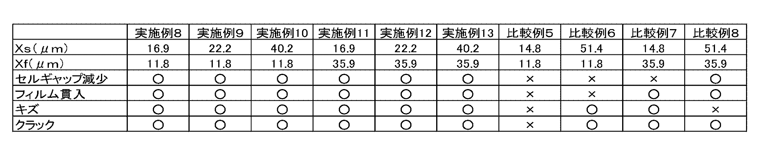
- Tables 1 and 2 are charts showing test results used for confirming the configuration related to the spacer.
- the examples and comparative examples in Tables 1 and 2 are configured identically except that the configurations related to the spacer and the alignment layer with which the spacer abuts are different. More specifically, in the light control films of these examples and comparative examples, the spacer 24 is provided only on the lower laminate 13, and the Vickers hardness value Xs of the spacer 24 is changed according to the manufacturing conditions related to the spacer 24. It was. Further, the Vickers hardness value Xf of the portion of the second laminate 12 with which the tip of the spacer 24 abuts was changed according to the conditions for manufacturing the alignment layer 23A.
- the spacer 24 is coated with the coating liquid related to the spacer 24 and then dried, and then selectively exposes a portion for manufacturing the spacer 24 by mask exposure using an exposure apparatus.
- this is a case of a positive type photoresist.
- a part other than the part for producing the spacer 24 is selectively exposed.
- the spacer 24 is selectively removed at an unexposed portion or exposed portion by development processing, and processing such as rinsing is performed, and processing such as drying is performed as necessary.
- exposure may be performed in a so-called half-cure state by heating in advance or in a heated environment.
- the heat treatment is performed. May accelerate the reaction.
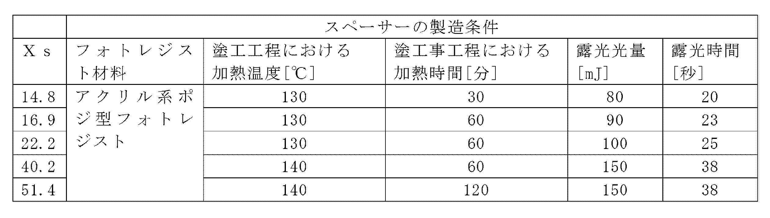
- the hardness Xs of the spacer 24 is set by selecting the photoresist material related to the spacer 24, setting the heating temperature and time in the coating process, exposure process, and development process, exposure light quantity and exposure time, and setting the mask cap. Can do.
- the Vickers hardness value Xs of the spacer 24 is 14.8, 16.9, 22.2, 40.2, and 51.4 depending on the setting of the heating temperature and time in the exposure process and the development process, respectively.
- a certain lower laminate 13 was produced (Table 3).
- the hardness is a measurement value obtained by setting the production conditions of the spacer 24 to manufacture the lower laminated body 13, and once manufacturing the light control film 10 using the lower laminated body 13 and then disassembling and measuring it. .
- this measurement is a measurement result based on an average value of 10 points which are obtained by measuring 12 points with each light control film and excluding the maximum value and the minimum value.
- the occupation ratio reduces the stress applied to each spacer, thereby reducing the phenomenon that the spacer 24 is crushed or the tip penetrates.
- increasing the occupation ratio deteriorates the transmittance. Or the shading rate deteriorates.
- the occupation ratio is desirably 0.5% or more and 10% or less.
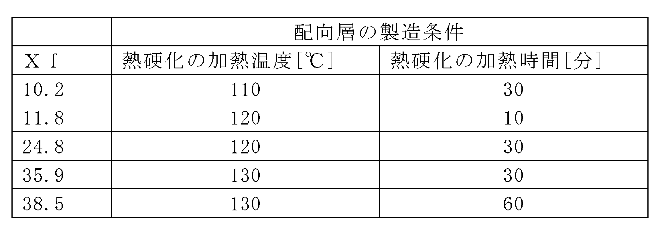
- the alignment layer 23A of the upper laminate 12 on which the spacer abuts is manufactured by applying a coating liquid, drying, and heat-curing.
- Vickers hardness value Xf was set by setting temperature, heating time, and the like.
- the upper side laminated body 12 whose Vickers hardness value Xf is 10.2, 11.8, 24.8, 35.9, 38.5 was manufactured (Table 4).
- the hardness Xf the upper laminate 12 having different hardness is produced for the orientation layer 23A of the upper laminate 12 which is a surface with which the spacer contacts by setting the creation conditions of the orientation layer 23A.
- the light control film 10 is once manufactured by the above, it is a measured value obtained by disassembling and measuring. Moreover, it is a measurement result by the average value of 10 points which are measured at 12 points and remain except for the maximum value and the minimum value.
- the Vickers hardness values Xs and Xf were measured using a PICODETOR HM500 manufactured by Helmut Fischer. The measurement was performed under the measurement conditions of a maximum load of 100 mN with an indentation speed of 300 mN / 20 sec, a release speed of 300 mN / 20 sec, and a creep time of 5 seconds.
- FIG. 5 is a cross-sectional view showing a laminated glass according to the second embodiment of the present invention. Since this laminated glass 101 is the same as the laminated glass 1 of the first embodiment except for the spacer 124, the same parts are denoted by the same reference numerals and the description thereof is omitted.
- the bead spacer 124 is provided to regulate the thickness of the liquid crystal layer 14.
- the bead spacer 124 can be widely applied to a configuration of an inorganic material such as silica, a configuration of an organic material, a configuration of a core-shell structure combining these, and the like. Moreover, you may comprise by the rod shape by cylindrical shape, prismatic shape, etc. other than the structure by spherical shape.
- the bead spacer 124 may be provided in the upper laminate 12 or may be provided in both the upper laminate 12 and the lower laminate 13.
- the bead spacer 124 may be provided on the alignment layer 23B.
- the bead spacer 124 is manufactured by a transparent member, the color may be adjusted by applying a colored material as necessary.
- the bead spacer 124 is formed by partially applying a coating solution produced by dispersing the bead spacer 124 in a solvent together with a resin component, and then sequentially performing drying and baking processes to thereby form the electrode 22B.
- the bead spacers 124 are randomly arranged on the top to keep it difficult to move, whereby the bead spacers 124 are arranged.
- the bead spacer 124 is arranged by the spacer arrangement step SP2-2 to manufacture a light control film, and the Vickers hardness value B of the portion of the upper laminate 12 with which the bead spacer 124 contacts is 11 Is set to be not less than 8 and not more than 35.9, and a multiplication value A ⁇ B of the occupation ratio A of the bead spacer 124 and the Vickers hardness value B is set to be 0.42 or more.
- the occupation ratio A is a ratio of the area of the bead spacer 124 to the area of the lower laminate 13 in a state where the lower laminate 13 is viewed in plan (a state seen from the vertical direction).
- the reliability regarding a bead spacer improves further compared with the past.
- the value of Vickers hardness is a measured value under the conditions described in the following examples and comparative examples.
- the Vickers hardness value B of the portion of the second laminate 12 with which the tip of the bead spacer 124 abuts is less than 11.8, the tip of the bead spacer 124 penetrates into the opposite surface due to the pressing force during use. As a result, the cell gap becomes non-uniform or local alignment failure occurs. Moreover, when the Vickers hardness value B of the said part exceeds 35.9, a crack will arise when the whole is bent.
- the tip of the bead spacer 124 penetrates into the opposing surface, and as a result, the cell gap becomes non-uniform or local An alignment failure occurs.
- the Vickers hardness value B of the portion of the upper laminate 12 with which the bead spacer 124 abuts is 11.8 or more and 35.9 or less, and the multiplication value A ⁇ B of the occupation ratio A and the Vickers hardness value B is 0.42 or more. If it is set so that these can be solved at once, the reliability of the bead spacer can be further improved as compared with the prior art.
- the Vickers hardness value B of the portion of the upper laminate 12 with which the bead spacer 124 abuts is 11.8 or more and 35.9 or less, the tip of the bead spacer 124 does not penetrate into the opposite surface due to the pressing force during use. And generation of cracks can be prevented. Furthermore, when the multiplication value A ⁇ B of the occupation ratio A and the Vickers hardness value B is 0.42 or more, the situation where the bead spacer is further penetrated is further reduced, and further, cracks when bent are reduced. Generation can be reduced.
- the Vickers hardness value B when the Vickers hardness value B is small, it can be said that the part is soft, and this facilitates penetration of the bead spacer. On the contrary, when the Vickers hardness value B is large, the part is hard and cracks are likely to occur when bent. Thereby, by setting the hardness value B to 11.8 or more and 35.9 or less, it is possible to reduce the situation in which the bead spacer penetrates, and further to reduce the occurrence of cracks when bent.
- the hardness value B is set in this way, the magnitude of the stress to one spacer varies depending on the number of spacers, and if the occupancy A as the index is small, the stress to one spacer As a result, even if the hardness value B is 11.8 or more and 35.9 or less, the bead spacer is likely to penetrate when the multiplication value A ⁇ B is less than 0.42. Further, when the occupation ratio A is small, the number of spacers is small, so that the stress concentration related to bending increases, and even if the hardness value B is 11.8 or more and 35.9 or less, the multiplication value. When A ⁇ B is less than 0.42, cracks are likely to occur.
- the Vickers hardness value B is set to 11.8 or more and 35.9 or less, and the multiplication value A ⁇ B is set to 0.42 or more, the reliability relating to the bead spacer can be further improved as compared with the related art.
- Tables 5 and 6 are charts showing test results used for confirmation of the configuration related to the bead spacers.
- the Examples and Comparative Examples in Tables 5 and 6 are configured identically except that the configurations related to the bead spacer and the alignment layer with which the bead spacer contacts are different. More specifically, in the light control films of these Examples and Comparative Examples, a bead spacer 124 is provided only in the lower laminate 13, and the occupation ratio A is variable depending on the selection of the size of the bead spacer 124 and the coating amount. did. Further, the Vickers hardness value B of the portion of the second laminate 12 with which the tip of the bead spacer 124 abuts was set according to the conditions for manufacturing the alignment layer 23A.
- the bead spacer 124 is coated on the electrode 22B by applying a coating solution prepared by dispersing the bead spacer 124 in a solvent together with a resin component, followed by drying, curing by ultraviolet irradiation, and firing.
- the bead spacers 124 are randomly arranged and are arranged to be difficult to move.
- the occupancy of the bead spacer 124 was adjusted by adjusting the amount charged into the coating solution and the coating film thickness of the coating solution.
- the density of the bead spacer 124 is set to 40 / mm 2 , 50 / mm 2 , 100 / mm 2 , and the bead spacer 124 has a spherical shape with diameters of 3 ⁇ m and 6 ⁇ m. Applied. Thus, the lower laminate 13 was manufactured with the occupation ratio A of 0.028%, 0.035%, 0.071%, 0.113%, and 0.141%.
- the bead spacer 124 Sekisui Chemical Co., Ltd. micropearl EX series was applied as the bead spacer 124.
- the base material 21B is a COP (cycloolefin polymer) film having a thickness of 100 ⁇ m and provided with a hard coat layer.
- the electrode 22B was manufactured with a thickness of 20 nm.
- the alignment layer 23B was manufactured by coating the coating liquid so as to have a dry film thickness of 100 nm and further thermosetting.
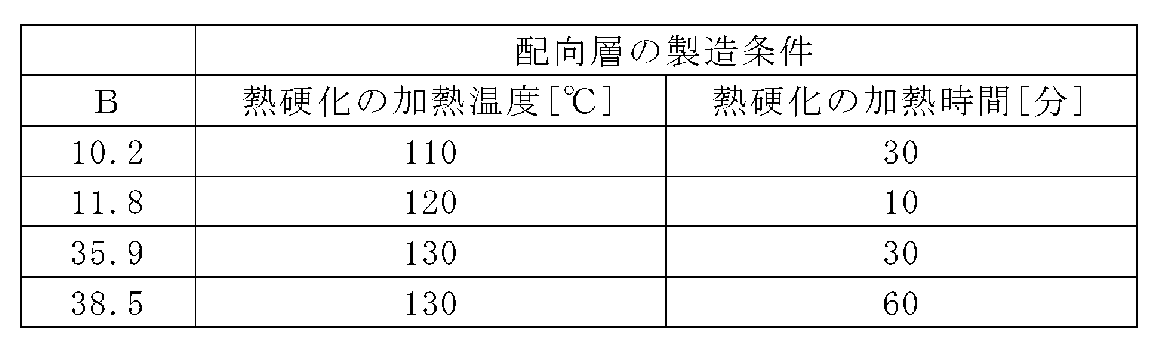
- the conditions for thermosetting after applying and drying the coating liquid Vickers hardness value B was set by setting (heating temperature, heating time) and the like.
- the upper side laminated body 12 whose Vickers hardness value B is 10.2, 11.8, 35.9, 38.5 was manufactured (Table 7).
- this hardness value B sets the preparation conditions of the orientation layer 23A, respectively, manufactures the upper laminated body 12 from which hardness differs about the orientation layer 23A, and once manufactures the light control film 110 by this upper laminate 12, It is a measured value obtained by disassembling. This measurement is a measurement result by measuring 12 points and averaging the remaining 10 points excluding the maximum and minimum values.
- the Vickers hardness value B was measured using a PICODETOR HM500 manufactured by Helmut Fischer. The measurement was performed under the measurement conditions of a maximum load of 100 mN with an indentation speed of 300 mN / 20 sec, a release speed of 300 mN / 20 sec, and a creep time of 5 seconds.
- the base material 21A and the electrode 22A of the upper laminate 12 were configured the same as the base material 21B and the electrode 22B of the lower laminate 13.
- the alignment layer 23A was configured the same as the alignment layer 23B except that the hardness value B was adjusted.
- the Vickers hardness value B of the portion of the second laminate 12 with which the bead spacer 124 abuts is 11.8 or more and 35.9 or less, and the occupation ratio A and the Vickers hardness value B are
- the multiplication value A ⁇ B is 0.42 or more, it was confirmed that film penetration could be prevented and cracks were not generated, and that it was possible to sufficiently ensure the reliability of the bead spacer.
Abstract
Description
また、例えばビーズスペーサーを適用することもできる。特許文献3、4には、このビーズスペーサーに関する工夫が提案されている。 Such a light control film is configured such that a spacer is provided on a transparent substrate constituting the liquid crystal cell, and the liquid crystal layer is held at a constant thickness by the spacer. In addition, the spacer has a configuration widely used in image display panels, and is manufactured in a column shape using, for example, a photoresist.
Further, for example, a bead spacer can be applied.
また、本発明者は、上記課題を解決するために鋭意研究を重ね、ビーズスペーサーが当接する面のビッカース硬度値B、平面視した状態でビーズスペーサーが占める面積の割合である占有率Aと硬度値Bとの乗算値A×Bを選定する、との着想に至り、本発明を完成するに至った。 The present inventor has intensively studied to solve the above-mentioned problems, and has come up with the idea that the Vickers hardness value Xs of the spacer and the Vickers hardness value Xf of the surface with which the spacer tip abuts are selected, respectively. It came to be completed.
In addition, the present inventor has conducted extensive research to solve the above-mentioned problems, and the Vickers hardness value B of the surface where the bead spacer abuts, the occupation ratio A and the hardness which are the ratio of the area occupied by the bead spacer in a plan view. The idea of selecting a multiplication value A × B with the value B was reached, and the present invention was completed.
前記第1の積層体は、
透明フィルム材による基材に、前記液晶層の厚みを保持するスペーサーが設けられ、
前記第1及び第2の積層体は、
前記スペーサーのビッカース硬度値Xsが16.9以上40.2以下であり、前記スペーサーの先端が当接する前記第2の積層体の部位のビッカース硬度値Xfが、11.8以上35.9以下である調光フィルム。 (1) A liquid crystal layer is sandwiched between first and second laminated bodies each including at least an alignment layer, and liquid crystal molecules related to the liquid crystal layer are driven by driving electrodes provided in the first and second laminated bodies. In the light control film that controls the transmitted light by controlling the orientation of
The first laminate is
A spacer that holds the thickness of the liquid crystal layer is provided on the substrate made of a transparent film material,
The first and second laminates are:
The Vickers hardness value Xs of the spacer is 16.9 or more and 40.2 or less, and the Vickers hardness value Xf of the portion of the second laminated body with which the tip of the spacer contacts is 11.8 or more and 35.9 or less. A light control film.
前記第1の積層体は、
透明フィルム材による基材に、前記液晶層の厚みを保持するビーズスペーサーが設けられ、
前記第1及び第2の積層体は、
前記ビーズスペーサーが当接する前記第2の積層体の部位のビッカース硬度値Bが11.8以上35.9以下であり、
前記第1の積層体を平面視した状態で、前記第1の積層体上で前記ビーズスペーサーが占める面積の比率である占有率Aと、前記ビッカース硬度値Bとの乗算値A×Bが、0.42以上である調光フィルム。 (2) A liquid crystal layer is sandwiched between first and second laminated bodies each including at least an alignment layer, and liquid crystal molecules related to the liquid crystal layer are driven by driving electrodes provided in the first and second laminated bodies. In the light control film that controls the transmitted light by controlling the orientation of
The first laminate is
A base material made of a transparent film material is provided with a bead spacer for maintaining the thickness of the liquid crystal layer,
The first and second laminates are:
The Vickers hardness value B of the portion of the second laminate in contact with the bead spacer is 11.8 or more and 35.9 or less,
In a state where the first laminate is viewed in plan, a multiplication value A × B of an occupation ratio A which is a ratio of an area occupied by the bead spacer on the first laminate and the Vickers hardness value B is: The light control film which is 0.42 or more.
少なくとも配向層を備えてなる第2の積層体を製造する第2の積層体製造工程と、
前記第1の積層体、液晶層、前記第2の積層体を積層してなる液晶セルを製造する液晶セル製造工程とを備え、
前記第1の積層体製造工程は、
基材に、前記液晶層の厚みを保持するスペーサーを製造するスペーサー製造工程を備え、
前記スペーサー製造工程は、
前記スペーサーのビッカース硬度値Xsが16.9以上40.2以下であるように前記スペーサーを製造し、
前記第2の積層体製造工程は、
前記スペーサーの先端が当接する前記第2の積層体の部位のビッカース硬度値Xfが、11.8以上35.9以下であるように前記第2の積層体を製造する調光フィルムの製造方法。 (4) a first laminate production process for producing a first laminate comprising at least an alignment layer;
A second laminate production process for producing a second laminate comprising at least an alignment layer;
A liquid crystal cell manufacturing process for manufacturing a liquid crystal cell formed by stacking the first stacked body, the liquid crystal layer, and the second stacked body,
The first laminate manufacturing process includes:
The substrate includes a spacer manufacturing process for manufacturing a spacer that maintains the thickness of the liquid crystal layer,
The spacer manufacturing process includes
The spacer is manufactured so that the Vickers hardness value Xs of the spacer is 16.9 or more and 40.2 or less,
The second laminate manufacturing process includes:
A method for producing a light control film, wherein the second laminate is produced such that a Vickers hardness value Xf of a portion of the second laminate in contact with a tip of the spacer is 11.8 or more and 35.9 or less.
少なくとも配向層を備えてなる第2の積層体を製造する第2の積層体製造工程と、
前記第1の積層体、液晶層、前記第2の積層体を積層してなる液晶セルを製造する液晶セル製造工程とを備え、
前記第1の積層体製造工程は、
基材に、前記液晶層の厚みを保持するビーズスペーサーを配置するビーズスペーサー配置工程を備え、
前記第2の積層体製造工程は、
前記ビーズスペーサーが当接する前記第2の積層体の部位のビッカース硬度値Bが11.8以上35.9以下であるように前記第2の積層体を製造し、
前記ビーズスペーサー配置工程は、
前記第1の積層体を平面視した状態で、前記第1の積層体上で前記ビーズスペーサーが占める面積の比率である占有率Aと、前記ビッカース硬度値Bとの乗算値A×Bが、0.42以上であるように前記ビーズスペーサーを配置する調光フィルムの製造方法。 (5) a first laminate production process for producing a first laminate comprising at least an alignment layer;
A second laminate production process for producing a second laminate comprising at least an alignment layer;
A liquid crystal cell manufacturing process for manufacturing a liquid crystal cell formed by stacking the first stacked body, the liquid crystal layer, and the second stacked body,
The first laminate manufacturing process includes:
The substrate comprises a bead spacer arrangement step of arranging a bead spacer for maintaining the thickness of the liquid crystal layer,
The second laminate manufacturing process includes:
Producing the second laminate so that the Vickers hardness value B of the portion of the second laminate in contact with the bead spacer is 11.8 or more and 35.9 or less,
The bead spacer arranging step includes
In a state where the first laminate is viewed in plan, a multiplication value A × B of an occupation ratio A which is a ratio of an area occupied by the bead spacer on the first laminate and the Vickers hardness value B is: The manufacturing method of the light control film which arrange | positions the said bead spacer so that it may be 0.42 or more.
〔合わせガラス〕
図1は、本発明の第1実施形態に係る合わせガラスを示す断面図である。この合わせガラス1は、例えば車両のウインドウに適用される合わせガラスであり、中間層4及び5をそれぞれ介して板ガラス2及び3により調光フィルム10を挟持して構成される。ここで板ガラス2、3は、この種の合わせガラスに適用可能な種々の材料を広く適用することができる。また中間層4、5は、調光フィルム10と板ガラス2、3との接着層として機能する構成であり、この種の合わせガラスに適用される種々の構成を広く適用することができ、例えば熱線遮蔽材としての機能を備えるようにしてもよい。 [First Embodiment]
[Laminated glass]
FIG. 1 is a cross-sectional view showing a laminated glass according to the first embodiment of the present invention. The
図2は、調光フィルムを示す断面図である。この調光フィルム10は、フィルム形状により形成され、合わせガラスに使用される場合の他、例えば調光を図る部位に貼り付けて使用される。なおこのような調光を図る部位に貼り付けて使用される場合は、例えば車両のリアウインド、建築物の窓ガラス、ショーケース、屋内の透明パーテーション等に配置して透過、不透明を切り替える場合等である。 [Light control film]
FIG. 2 is a cross-sectional view showing a light control film. The
図4は、調光フィルム10の製造工程を示すフローチャートである。液晶セル15は、第1の積層体製造工程SP2において、第1の積層体13が製造される。
第1の積層体製造工程SP2においては、電極製造工程SP2-1において、基材21Bにスパッタリング等によりITOによる透明電極22Bが製造される。
続くスペーサー製造工程SP2-2において、スペーサー24に係る塗工液(フォトレジスト)を塗工した後、乾燥、露光して現像することにより、スペーサー24が製造される。
また続いて配向層製造工程SP2-3において、配向層23Bに係る塗工液を塗工して乾燥した後、紫外線の照射により硬化させ、これにより配向層23Bが製造される。これらによりこの実施形態では、第1の積層体13が製造される。 〔Manufacturing process〕
FIG. 4 is a flowchart showing the manufacturing process of the
In the first laminate manufacturing process SP2, in the electrode manufacturing process SP2-1, the
In the subsequent spacer manufacturing step SP2-2, the coating liquid (photoresist) relating to the
Subsequently, in the alignment layer manufacturing step SP2-3, the coating liquid for the
The
ここでこの実施形態では、図4に示す工程によりフォトレジストを使用して円柱形状又は円錐台形状によりスペーサー24が形成される。このようにしてスペーサー24を製造して、この実施形態では、スペーサー24のビッカース硬度値Xsが16.9以上40.2以下であり、スペーサー24の先端が当接する第2の積層体12の部位のビッカース硬度値Xfが、11.8以上35.9以下であるように設定され、これによりスペーサーに関する信頼性を従来に比して一段と向上する。なお、ビッカース硬度の値は、以下の実施例に記載の条件における測定値である。 [Detailed configuration of spacer]
Here, in this embodiment, the
表1及び表2は、このスペーサーに関する構成の確認に供した試験結果を示す図表である。この表1及び表2における実施例、比較例は、スペーサー及びこのスペーサーが当接する配向層に関する構成が異なる点を除いて、同一に構成される。より具体的に、これら実施例、比較例の調光フィルムは、下側積層体13にのみスペーサー24を設けるようにし、このスペーサー24に係る製造条件により、スペーサー24のビッカース硬度値Xsを変化させた。また配向層23Aを製造する際の条件により、スペーサー24の先端が当接する第2の積層体12の部位のビッカース硬度値Xfを変化させた。 〔Test results〕
Tables 1 and 2 are charts showing test results used for confirming the configuration related to the spacer. The examples and comparative examples in Tables 1 and 2 are configured identically except that the configurations related to the spacer and the alignment layer with which the spacer abuts are different. More specifically, in the light control films of these examples and comparative examples, the

〔合わせガラス〕
図5は、本発明の第2実施形態に係る合わせガラスを示す断面図である。この合わせガラス101は、第1実施形態の合わせガラス1と、スペーサー124以外同様であるので、同様の部分は同一の符号を付し、説明を省略する。 [Second Embodiment]
[Laminated glass]
FIG. 5 is a cross-sectional view showing a laminated glass according to the second embodiment of the present invention. Since this
調光フィルム110の製造工程も第1実施形態の図4で示す工程と同様であるので、同様の工程の説明を省略する。第1実施形態と異なるのは、第1実施形態のスペーサ製造工程SP2-2が、第2実施形態ではスペーサー配置工程SP2-2で、ビーズスペーサー124を配置する点である。 〔Manufacturing process〕
Since the manufacturing process of the
ここでこの実施形態では、スペーサー配置工程SP2-2によりビーズスペーサー124を配置して調光フィルムを製造するようにして、ビーズスペーサー124が当接する上側積層体12の部位のビッカース硬度値Bが11.8以上35.9以下であるように設定され、ビーズスペーサー124の占有率Aと、ビッカース硬度値Bとの乗算値A×Bが、0.42以上であるように設定される。なおここで占有率Aは、下側積層体13を平面視した状態(鉛直方向から見た状態)で、下側積層体13の面積に対するビーズスペーサー124の面積の占める割合である。これによりこの実施形態では、ビーズスペーサーに関する信頼性を従来に比して一段と向上する。なお、ビッカース硬度の値は、以下の実施例、比較例に記載の条件における測定値である。 [Detailed configuration of bead spacer]
Here, in this embodiment, the
表5、表6は、このビーズスペーサーに関する構成の確認に供した試験結果を示す図表である。この表5、表6における実施例、比較例は、ビーズスペーサー及びこのビーズスペーサーが当接する配向層に関する構成が異なる点を除いて、同一に構成される。より具体的に、これら実施例、比較例の調光フィルムは、下側積層体13にのみビーズスペーサー124を設けるようにし、このビーズスペーサー124の大きさの選定、塗布量により占有率Aを可変した。また配向層23Aを製造する際の条件により、ビーズスペーサー124の先端が当接する第2の積層体12の部位のビッカース硬度値Bを設定した。 〔Test results〕
Tables 5 and 6 are charts showing test results used for confirmation of the configuration related to the bead spacers. The Examples and Comparative Examples in Tables 5 and 6 are configured identically except that the configurations related to the bead spacer and the alignment layer with which the bead spacer contacts are different. More specifically, in the light control films of these Examples and Comparative Examples, a


以上、本発明の実施に好適な具体的な構成を詳述したが、本発明は、本発明の趣旨を逸脱しない範囲で、上述の実施形態を種々に変更することができる。 [Other Embodiments]
As mentioned above, although the specific structure suitable for implementation of this invention was explained in full detail, this invention can be variously changed in the range which does not deviate from the meaning of this invention.
2、3 板ガラス
4、5 中間層
10、110 調光フィルム
12 上側積層体
13 下側積層体
14 液晶層
14A 液晶分子
15 液晶セル
16、17 直線偏光板
18、19 位相差フィルム
21A、21B 基材
22A、22B 電極
23A、23B 配向層
24 スペーサー
25 シール材
124 ビーズスペーサー DESCRIPTION OF SYMBOLS 1,101
Claims (5)
- 少なくとも配向層を備えてなる第1及び第2の積層体により液晶層を挟持し、前記第1及び又は第2の積層体に設けられた電極の駆動により前記液晶層に係る液晶分子の配向を制御して透過光を制御する調光フィルムにおいて、
前記第1の積層体は、
透明フィルム材による基材に、前記液晶層の厚みを保持するスペーサーが設けられ、
前記第1及び第2の積層体は、
前記スペーサーのビッカース硬度値Xsが16.9以上40.2以下であり、前記スペーサーの先端が当接する前記第2の積層体の部位のビッカース硬度値Xfが、11.8以上35.9以下である
調光フィルム。 The liquid crystal layer is sandwiched between the first and second stacked bodies including at least an alignment layer, and the liquid crystal molecules are aligned with respect to the liquid crystal layer by driving the electrodes provided in the first and second stacked bodies. In a light control film that controls transmitted light by controlling,
The first laminate is
A spacer that holds the thickness of the liquid crystal layer is provided on the substrate made of a transparent film material,
The first and second laminates are:
The Vickers hardness value Xs of the spacer is 16.9 or more and 40.2 or less, and the Vickers hardness value Xf of the portion of the second laminated body with which the tip of the spacer contacts is 11.8 or more and 35.9 or less. There is a light control film. - 少なくとも配向層を備えてなる第1及び第2の積層体により液晶層を挟持し、前記第1及び又は第2の積層体に設けられた電極の駆動により前記液晶層に係る液晶分子の配向を制御して透過光を制御する調光フィルムにおいて、
前記第1の積層体は、
透明フィルム材による基材に、前記液晶層の厚みを保持するビーズスペーサーが設けられ、
前記第1及び第2の積層体は、
前記ビーズスペーサーが当接する前記第2の積層体の部位のビッカース硬度値Bが11.8以上35.9以下であり、
前記第1の積層体を平面視した状態で、前記第1の積層体上で前記ビーズスペーサーが占める面積の比率である占有率Aと、前記ビッカース硬度値Bとの乗算値A×Bが、0.42以上である
調光フィルム。 The liquid crystal layer is sandwiched between the first and second stacked bodies including at least an alignment layer, and the liquid crystal molecules are aligned with respect to the liquid crystal layer by driving the electrodes provided in the first and second stacked bodies. In a light control film that controls transmitted light by controlling,
The first laminate is
A base material made of a transparent film material is provided with a bead spacer for maintaining the thickness of the liquid crystal layer,
The first and second laminates are:
The Vickers hardness value B of the portion of the second laminate in contact with the bead spacer is 11.8 or more and 35.9 or less,
In a state where the first laminate is viewed in plan, a multiplication value A × B of an occupation ratio A which is a ratio of an area occupied by the bead spacer on the first laminate and the Vickers hardness value B is: The light control film which is 0.42 or more. - 請求項1または2に記載の調光フィルムを板ガラスにより挟持して形成された
合わせガラス。 A laminated glass formed by sandwiching the light control film according to claim 1 or 2 between plate glasses. - 少なくとも配向層を備えてなる第1の積層体を製造する第1の積層体製造工程と、
少なくとも配向層を備えてなる第2の積層体を製造する第2の積層体製造工程と、
前記第1の積層体、液晶層、前記第2の積層体を積層してなる液晶セルを製造する液晶セル製造工程とを備え、
前記第1の積層体製造工程は、
基材に、前記液晶層の厚みを保持するスペーサーを製造するスペーサー製造工程を備え、
前記スペーサー製造工程は、
前記スペーサーのビッカース硬度値Xsが16.9以上40.2以下であるように前記スペーサーを製造し、
前記第2の積層体製造工程は、
前記スペーサーの先端が当接する前記第2の積層体の部位のビッカース硬度値Xfが、11.8以上35.9以下であるように前記第2の積層体を製造する
調光フィルムの製造方法。 A first laminate production process for producing a first laminate comprising at least an alignment layer;
A second laminate production process for producing a second laminate comprising at least an alignment layer;
A liquid crystal cell manufacturing process for manufacturing a liquid crystal cell formed by stacking the first stacked body, the liquid crystal layer, and the second stacked body,
The first laminate manufacturing process includes:
The substrate includes a spacer manufacturing process for manufacturing a spacer that maintains the thickness of the liquid crystal layer,
The spacer manufacturing process includes
The spacer is manufactured so that the Vickers hardness value Xs of the spacer is 16.9 or more and 40.2 or less,
The second laminate manufacturing process includes:
A method for producing a light control film, wherein the second laminate is produced such that a Vickers hardness value Xf of a portion of the second laminate in contact with a tip of the spacer is 11.8 or more and 35.9 or less. - 少なくとも配向層を備えてなる第1の積層体を製造する第1の積層体製造工程と、
少なくとも配向層を備えてなる第2の積層体を製造する第2の積層体製造工程と、
前記第1の積層体、液晶層、前記第2の積層体を積層してなる液晶セルを製造する液晶セル製造工程とを備え、
前記第1の積層体製造工程は、
基材に、前記液晶層の厚みを保持するビーズスペーサーを配置するビーズスペーサー配置工程を備え、
前記第2の積層体製造工程は、
前記ビーズスペーサーが当接する前記第2の積層体の部位のビッカース硬度値Bが11.8以上35.9以下であるように前記第2の積層体を製造し、
前記ビーズスペーサー配置工程は、
前記第1の積層体を平面視した状態で、前記第1の積層体上で前記ビーズスペーサーが占める面積の比率である占有率Aと、前記ビッカース硬度値Bとの乗算値A×Bが、0.42以上であるように前記ビーズスペーサーを配置する
調光フィルムの製造方法。 A first laminate production process for producing a first laminate comprising at least an alignment layer;
A second laminate production process for producing a second laminate comprising at least an alignment layer;
A liquid crystal cell manufacturing process for manufacturing a liquid crystal cell formed by stacking the first stacked body, the liquid crystal layer, and the second stacked body,
The first laminate manufacturing process includes:
The substrate comprises a bead spacer arrangement step of arranging a bead spacer for maintaining the thickness of the liquid crystal layer,
The second laminate manufacturing process includes:
Producing the second laminate so that the Vickers hardness value B of the portion of the second laminate in contact with the bead spacer is 11.8 or more and 35.9 or less,
The bead spacer arranging step includes
In a state where the first laminate is viewed in plan, a multiplication value A × B of an occupation ratio A which is a ratio of an area occupied by the bead spacer on the first laminate and the Vickers hardness value B is: The manufacturing method of the light control film which arrange | positions the said bead spacer so that it may be 0.42 or more.
Priority Applications (5)
| Application Number | Priority Date | Filing Date | Title |
|---|---|---|---|
| US16/094,330 US10732464B2 (en) | 2016-04-21 | 2017-04-20 | Light control film, laminated glass and method for producing light control film |
| KR1020187031683A KR102226630B1 (en) | 2016-04-21 | 2017-04-20 | Manufacturing method of dimming film, laminated glass, and dimming film |
| EP17786029.3A EP3447566B1 (en) | 2016-04-21 | 2017-04-20 | Light control film, laminated glass and method for producing light control film |
| CN201780024336.3A CN109073923B (en) | 2016-04-21 | 2017-04-20 | Light-adjusting film, laminated glass and method for manufacturing light-adjusting film |
| US16/913,293 US11150521B2 (en) | 2016-04-21 | 2020-06-26 | Light control film, laminated glass and method for producing light control film |
Applications Claiming Priority (4)
| Application Number | Priority Date | Filing Date | Title |
|---|---|---|---|
| JP2016085392A JP6065142B1 (en) | 2016-04-21 | 2016-04-21 | Light control film, laminated glass, and method for manufacturing light control film |
| JP2016-085392 | 2016-04-21 | ||
| JP2016087131A JP6065143B1 (en) | 2016-04-25 | 2016-04-25 | Light control film, laminated glass, and method for manufacturing light control film |
| JP2016-087131 | 2016-04-25 |
Related Child Applications (2)
| Application Number | Title | Priority Date | Filing Date |
|---|---|---|---|
| US16/094,330 A-371-Of-International US10732464B2 (en) | 2016-04-21 | 2017-04-20 | Light control film, laminated glass and method for producing light control film |
| US16/913,293 Division US11150521B2 (en) | 2016-04-21 | 2020-06-26 | Light control film, laminated glass and method for producing light control film |
Publications (1)
| Publication Number | Publication Date |
|---|---|
| WO2017183692A1 true WO2017183692A1 (en) | 2017-10-26 |
Family
ID=60116186
Family Applications (1)
| Application Number | Title | Priority Date | Filing Date |
|---|---|---|---|
| PCT/JP2017/015895 WO2017183692A1 (en) | 2016-04-21 | 2017-04-20 | Light control film, laminated glass and method for producing light control film |
Country Status (5)
| Country | Link |
|---|---|
| US (2) | US10732464B2 (en) |
| EP (1) | EP3447566B1 (en) |
| KR (1) | KR102226630B1 (en) |
| CN (1) | CN109073923B (en) |
| WO (1) | WO2017183692A1 (en) |
Cited By (12)
| Publication number | Priority date | Publication date | Assignee | Title |
|---|---|---|---|---|
| WO2019103115A1 (en) * | 2017-11-24 | 2019-05-31 | 大日本印刷株式会社 | Laminated glass and liquid crystal film |
| KR20200078545A (en) * | 2017-11-02 | 2020-07-01 | 다이니폰 인사츠 가부시키가이샤 | Manufacturing method of laminated glass, laminated glass, dimming film |
| US10705363B2 (en) | 2017-07-13 | 2020-07-07 | Cardinal Ig Company | Electrical connection configurations for privacy glazing structures |
| US10866480B2 (en) | 2017-04-20 | 2020-12-15 | Cardinal Ig Company | High performance privacy glazing structures |
| US10968684B2 (en) | 2018-08-17 | 2021-04-06 | Cardinal Ig Company | Privacy glazing structure with asymetrical pane offsets for electrical connection configurations |
| US11111720B2 (en) | 2019-02-08 | 2021-09-07 | Cardinal Ig Company | Low power driver for privacy glazing |
| US11175523B2 (en) | 2019-04-29 | 2021-11-16 | Cardinal Ig Company | Staggered driving electrical control of a plurality of electrically controllable privacy glazing structures |
| US11243421B2 (en) | 2018-05-09 | 2022-02-08 | Cardinal Ig Company | Electrically controllable privacy glazing with energy recapturing driver |
| US11325352B2 (en) | 2019-04-29 | 2022-05-10 | Cardinal Ig Company | Leakage current detection and control for one or more electrically controllable privacy glazing structures |
| US11360364B2 (en) | 2017-11-06 | 2022-06-14 | Cardinal Ig Company | Privacy glazing system with discrete electrical driver |
| US11448910B2 (en) | 2019-04-29 | 2022-09-20 | Cardinal Ig Company | Systems and methods for operating one or more electrically controllable privacy glazing structures |
| US11474385B1 (en) | 2018-12-02 | 2022-10-18 | Cardinal Ig Company | Electrically controllable privacy glazing with ultralow power consumption comprising a liquid crystal material having a light transmittance that varies in response to application of an electric field |
Families Citing this family (7)
| Publication number | Priority date | Publication date | Assignee | Title |
|---|---|---|---|---|
| US10670911B2 (en) * | 2016-05-20 | 2020-06-02 | Sharp Kabushiki Kaisha | Liquid crystal display panel and liquid crystal display device |
| JP6414312B1 (en) * | 2017-11-27 | 2018-10-31 | 凸版印刷株式会社 | Light control unit and window light control plate |
| WO2019142719A1 (en) | 2018-01-17 | 2019-07-25 | 積水化学工業株式会社 | Dimming laminate and resin spacer for dimming laminate |
| CN111624800A (en) * | 2020-06-29 | 2020-09-04 | 京东方科技集团股份有限公司 | Light modulation structure, manufacturing method thereof and light modulation module |
| KR20230135924A (en) | 2022-03-17 | 2023-09-26 | 동우 화인켐 주식회사 | Optical laminate, and manufacturing method for the same, and smart window including the same |
| KR20230138729A (en) | 2022-03-24 | 2023-10-05 | 동우 화인켐 주식회사 | Transmittance variable optical laminate and manufacturing method for the same, and smart window including the same |
| KR20230166461A (en) | 2022-05-31 | 2023-12-07 | 동우 화인켐 주식회사 | Transmittance variable optical laminate and manufacturing method for the same, and smart window including the same |
Citations (5)
| Publication number | Priority date | Publication date | Assignee | Title |
|---|---|---|---|---|
| JP2001100188A (en) * | 1999-09-30 | 2001-04-13 | Ricoh Co Ltd | Liquid crystal display element |
| JP2001180264A (en) * | 1999-12-24 | 2001-07-03 | Asahi Glass Co Ltd | Liquid crystal light control window for vehicle |
| JP2004069749A (en) * | 2002-08-01 | 2004-03-04 | Casio Comput Co Ltd | Liquid crystal display element |
| US20090091677A1 (en) * | 2007-10-05 | 2009-04-09 | Jun Beom Cho | Liquid crystal display and method for manufacturing the same |
| JP2012203184A (en) * | 2011-03-25 | 2012-10-22 | Toppan Printing Co Ltd | Color filter substrate and liquid crystal display device having the same |
Family Cites Families (22)
| Publication number | Priority date | Publication date | Assignee | Title |
|---|---|---|---|---|
| JPS62286023A (en) | 1986-06-04 | 1987-12-11 | Toyota Motor Corp | Production of liquid crystal cell |
| JP2527467B2 (en) | 1988-10-29 | 1996-08-21 | シャープ株式会社 | Liquid crystal display manufacturing method |
| JPH0347392A (en) | 1989-07-12 | 1991-02-28 | Natl House Ind Co Ltd | liquid crystal panel |
| JP3158667B2 (en) * | 1991-08-01 | 2001-04-23 | セイコーエプソン株式会社 | Method of manufacturing liquid crystal display element and method of reproducing liquid crystal display element |
| JPH0817288A (en) * | 1994-07-04 | 1996-01-19 | Matsushita Electric Ind Co Ltd | Transparent touch panel |
| JPH08184273A (en) | 1994-12-27 | 1996-07-16 | Ohbayashi Corp | Lighting control glass window |
| JP3299869B2 (en) | 1995-09-27 | 2002-07-08 | シャープ株式会社 | Liquid crystal display device and manufacturing method thereof |
| JPH112820A (en) * | 1997-06-13 | 1999-01-06 | Sharp Corp | Liquid crystal display device |
| JPH112821A (en) * | 1997-06-13 | 1999-01-06 | Sony Corp | Liquid crystal element and its manufacture |
| US7411211B1 (en) * | 1999-07-22 | 2008-08-12 | Semiconductor Energy Laboratory Co., Ltd. | Contact structure and semiconductor device |
| JP2001083525A (en) * | 1999-09-09 | 2001-03-30 | Canon Inc | Color filter with spacer, its production and liquid crystal device using that color filter |
| US6812977B1 (en) * | 1999-11-22 | 2004-11-02 | Minolta Co., Ltd. | Liquid crystal element |
| JP2001174619A (en) * | 1999-12-14 | 2001-06-29 | Shin Sti Technology Kk | Color filter for liquid crystal |
| JP2002198374A (en) * | 2000-10-16 | 2002-07-12 | Sharp Corp | Semiconductor device and its fabrication method |
| JP4024516B2 (en) * | 2001-10-18 | 2007-12-19 | シャープ株式会社 | Liquid crystal display |
| JP4929578B2 (en) * | 2003-11-10 | 2012-05-09 | 大日本印刷株式会社 | Liquid crystal display |
| KR101114233B1 (en) * | 2005-04-29 | 2012-03-06 | 엘지디스플레이 주식회사 | Liquid Crystal Display Panel and Method for Fabricating Thereof |
| JP4901198B2 (en) * | 2005-11-28 | 2012-03-21 | 大日本印刷株式会社 | Substrate for display device with spacer |
| JP4774954B2 (en) * | 2005-11-28 | 2011-09-21 | 大日本印刷株式会社 | Substrate for display device with spacer |
| JP5749021B2 (en) * | 2009-02-13 | 2015-07-15 | 日立化成株式会社 | Light control film |
| CN104714338A (en) * | 2013-12-16 | 2015-06-17 | 群创光电股份有限公司 | Liquid crystal display panel |
| JP6413320B2 (en) * | 2014-04-28 | 2018-10-31 | 凸版印刷株式会社 | Column spacer for color filter for liquid crystal display device, color filter for liquid crystal display device, and liquid crystal display device |
-
2017
- 2017-04-20 EP EP17786029.3A patent/EP3447566B1/en active Active
- 2017-04-20 WO PCT/JP2017/015895 patent/WO2017183692A1/en active Application Filing
- 2017-04-20 KR KR1020187031683A patent/KR102226630B1/en active IP Right Grant
- 2017-04-20 US US16/094,330 patent/US10732464B2/en active Active
- 2017-04-20 CN CN201780024336.3A patent/CN109073923B/en active Active
-
2020
- 2020-06-26 US US16/913,293 patent/US11150521B2/en active Active
Patent Citations (5)
| Publication number | Priority date | Publication date | Assignee | Title |
|---|---|---|---|---|
| JP2001100188A (en) * | 1999-09-30 | 2001-04-13 | Ricoh Co Ltd | Liquid crystal display element |
| JP2001180264A (en) * | 1999-12-24 | 2001-07-03 | Asahi Glass Co Ltd | Liquid crystal light control window for vehicle |
| JP2004069749A (en) * | 2002-08-01 | 2004-03-04 | Casio Comput Co Ltd | Liquid crystal display element |
| US20090091677A1 (en) * | 2007-10-05 | 2009-04-09 | Jun Beom Cho | Liquid crystal display and method for manufacturing the same |
| JP2012203184A (en) * | 2011-03-25 | 2012-10-22 | Toppan Printing Co Ltd | Color filter substrate and liquid crystal display device having the same |
Cited By (24)
| Publication number | Priority date | Publication date | Assignee | Title |
|---|---|---|---|---|
| US10866480B2 (en) | 2017-04-20 | 2020-12-15 | Cardinal Ig Company | High performance privacy glazing structures |
| US11774825B2 (en) | 2017-04-20 | 2023-10-03 | Cardinal Ig Company | High performance privacy glazing structures |
| US10705363B2 (en) | 2017-07-13 | 2020-07-07 | Cardinal Ig Company | Electrical connection configurations for privacy glazing structures |
| US11934055B2 (en) | 2017-07-13 | 2024-03-19 | Cardinal Ig Company | Electrical connection configurations for privacy glazing structures |
| US10989945B2 (en) | 2017-07-13 | 2021-04-27 | Cardinal Ig Company | Electrical connection configurations for privacy glazing structures |
| US11467439B2 (en) | 2017-07-13 | 2022-10-11 | Cardinal Ig Company | Electrical connection configurations for privacy glazing structures |
| EP3770132A4 (en) * | 2017-11-02 | 2022-03-02 | Dai Nippon Printing Co., Ltd. | Method for manufacturing laminated glass, laminated glass and light control film |
| KR20200078545A (en) * | 2017-11-02 | 2020-07-01 | 다이니폰 인사츠 가부시키가이샤 | Manufacturing method of laminated glass, laminated glass, dimming film |
| KR102607588B1 (en) | 2017-11-02 | 2023-11-30 | 다이니폰 인사츠 가부시키가이샤 | Manufacturing method of laminated glass, laminated glass, dimming film |
| US11619839B2 (en) | 2017-11-02 | 2023-04-04 | Dai Nippon Printing Co., Ltd. | Method for manufacturing laminated glass, laminated glass and light control film |
| US11360364B2 (en) | 2017-11-06 | 2022-06-14 | Cardinal Ig Company | Privacy glazing system with discrete electrical driver |
| US11698562B2 (en) | 2017-11-06 | 2023-07-11 | Cardinal Ig Company | Privacy glazing system with discrete electrical driver |
| WO2019103115A1 (en) * | 2017-11-24 | 2019-05-31 | 大日本印刷株式会社 | Laminated glass and liquid crystal film |
| JPWO2019103115A1 (en) * | 2017-11-24 | 2020-11-19 | 大日本印刷株式会社 | Laminated glass, liquid crystal film |
| JP7440266B2 (en) | 2017-11-24 | 2024-02-28 | 大日本印刷株式会社 | Laminated glass, liquid crystal film |
| US11243421B2 (en) | 2018-05-09 | 2022-02-08 | Cardinal Ig Company | Electrically controllable privacy glazing with energy recapturing driver |
| US10968684B2 (en) | 2018-08-17 | 2021-04-06 | Cardinal Ig Company | Privacy glazing structure with asymetrical pane offsets for electrical connection configurations |
| US11474385B1 (en) | 2018-12-02 | 2022-10-18 | Cardinal Ig Company | Electrically controllable privacy glazing with ultralow power consumption comprising a liquid crystal material having a light transmittance that varies in response to application of an electric field |
| US11111720B2 (en) | 2019-02-08 | 2021-09-07 | Cardinal Ig Company | Low power driver for privacy glazing |
| US11681170B2 (en) | 2019-04-29 | 2023-06-20 | Cardinal Ig Company | Staggered driving electrical control of a plurality of electrically controllable privacy glazing structures |
| US11826986B2 (en) | 2019-04-29 | 2023-11-28 | Cardinal Ig Company | Leakage current detection and control for one or more electrically controllable privacy glazing structures |
| US11325352B2 (en) | 2019-04-29 | 2022-05-10 | Cardinal Ig Company | Leakage current detection and control for one or more electrically controllable privacy glazing structures |
| US11175523B2 (en) | 2019-04-29 | 2021-11-16 | Cardinal Ig Company | Staggered driving electrical control of a plurality of electrically controllable privacy glazing structures |
| US11448910B2 (en) | 2019-04-29 | 2022-09-20 | Cardinal Ig Company | Systems and methods for operating one or more electrically controllable privacy glazing structures |
Also Published As
| Publication number | Publication date |
|---|---|
| CN109073923A (en) | 2018-12-21 |
| EP3447566A4 (en) | 2019-10-02 |
| US20200326577A1 (en) | 2020-10-15 |
| CN109073923B (en) | 2021-11-26 |
| US20190121186A1 (en) | 2019-04-25 |
| KR20180132782A (en) | 2018-12-12 |
| EP3447566A1 (en) | 2019-02-27 |
| US11150521B2 (en) | 2021-10-19 |
| US10732464B2 (en) | 2020-08-04 |
| KR102226630B1 (en) | 2021-03-12 |
| EP3447566B1 (en) | 2020-05-27 |
Similar Documents
| Publication | Publication Date | Title |
|---|---|---|
| WO2017183692A1 (en) | Light control film, laminated glass and method for producing light control film | |
| JP7435667B2 (en) | Light control film and laminated glass | |
| JP5910788B1 (en) | Light control film, laminated glass, and method for manufacturing light control film | |
| JP6065142B1 (en) | Light control film, laminated glass, and method for manufacturing light control film | |
| US20230350249A1 (en) | Light control film and laminated glass | |
| JP6665661B2 (en) | Light control film, method for manufacturing light control film | |
| JP6065143B1 (en) | Light control film, laminated glass, and method for manufacturing light control film | |
| JP2017151167A (en) | Dimming film, laminated glass and method for manufacturing dimming film | |
| JP6048606B1 (en) | Light control film and method of manufacturing light control film | |
| JP2017181825A (en) | Light control film and window | |
| JP6183492B1 (en) | Light control film and method of manufacturing light control film | |
| JP6065144B1 (en) | Light control film | |
| WO2017170578A1 (en) | Light-controlling film and method for manufacturing light-controlling film | |
| JP2017198731A (en) | Lighting control film and manufacturing method of lighting control film | |
| JP2017181826A (en) | Light control film and window | |
| JP2018049231A (en) | Liquid crystal cell and method for manufacturing liquid crystal cell | |
| JP2018049232A (en) | Liquid crystal cell | |
| JP2017181808A (en) | Light control film and production method of light control film |
Legal Events
| Date | Code | Title | Description |
|---|---|---|---|
| NENP | Non-entry into the national phase |
Ref country code: DE |
|
| ENP | Entry into the national phase |
Ref document number: 20187031683 Country of ref document: KR Kind code of ref document: A |
|
| WWE | Wipo information: entry into national phase |
Ref document number: 2017786029 Country of ref document: EP |
|
| ENP | Entry into the national phase |
Ref document number: 2017786029 Country of ref document: EP Effective date: 20181121 |
|
| 121 | Ep: the epo has been informed by wipo that ep was designated in this application |
Ref document number: 17786029 Country of ref document: EP Kind code of ref document: A1 |