WO2017181724A1 - 电子元件漏件检测方法和系统 - Google Patents
电子元件漏件检测方法和系统 Download PDFInfo
- Publication number
- WO2017181724A1 WO2017181724A1 PCT/CN2016/112888 CN2016112888W WO2017181724A1 WO 2017181724 A1 WO2017181724 A1 WO 2017181724A1 CN 2016112888 W CN2016112888 W CN 2016112888W WO 2017181724 A1 WO2017181724 A1 WO 2017181724A1
- Authority
- WO
- WIPO (PCT)
- Prior art keywords
- image
- edge
- electronic component
- edge image
- test
- Prior art date
- Legal status (The legal status is an assumption and is not a legal conclusion. Google has not performed a legal analysis and makes no representation as to the accuracy of the status listed.)
- Ceased
Links
Images


Classifications
-
- G—PHYSICS
- G01—MEASURING; TESTING
- G01N—INVESTIGATING OR ANALYSING MATERIALS BY DETERMINING THEIR CHEMICAL OR PHYSICAL PROPERTIES
- G01N21/00—Investigating or analysing materials by the use of optical means, i.e. using sub-millimetre waves, infrared, visible or ultraviolet light
- G01N21/84—Systems specially adapted for particular applications
- G01N21/88—Investigating the presence of flaws or contamination
-
- G—PHYSICS
- G06—COMPUTING OR CALCULATING; COUNTING
- G06T—IMAGE DATA PROCESSING OR GENERATION, IN GENERAL
- G06T7/00—Image analysis
- G06T7/0002—Inspection of images, e.g. flaw detection
- G06T7/0004—Industrial image inspection
- G06T7/0008—Industrial image inspection checking presence/absence
-
- G—PHYSICS
- G01—MEASURING; TESTING
- G01N—INVESTIGATING OR ANALYSING MATERIALS BY DETERMINING THEIR CHEMICAL OR PHYSICAL PROPERTIES
- G01N21/00—Investigating or analysing materials by the use of optical means, i.e. using sub-millimetre waves, infrared, visible or ultraviolet light
- G01N21/84—Systems specially adapted for particular applications
- G01N21/88—Investigating the presence of flaws or contamination
- G01N21/8851—Scan or image signal processing specially adapted therefor, e.g. for scan signal adjustment, for detecting different kinds of defects, for compensating for structures, markings, edges
-
- G—PHYSICS
- G01—MEASURING; TESTING
- G01N—INVESTIGATING OR ANALYSING MATERIALS BY DETERMINING THEIR CHEMICAL OR PHYSICAL PROPERTIES
- G01N21/00—Investigating or analysing materials by the use of optical means, i.e. using sub-millimetre waves, infrared, visible or ultraviolet light
- G01N21/84—Systems specially adapted for particular applications
- G01N21/88—Investigating the presence of flaws or contamination
- G01N21/95—Investigating the presence of flaws or contamination characterised by the material or shape of the object to be examined
-
- G—PHYSICS
- G06—COMPUTING OR CALCULATING; COUNTING
- G06T—IMAGE DATA PROCESSING OR GENERATION, IN GENERAL
- G06T7/00—Image analysis
-
- G—PHYSICS
- G01—MEASURING; TESTING
- G01N—INVESTIGATING OR ANALYSING MATERIALS BY DETERMINING THEIR CHEMICAL OR PHYSICAL PROPERTIES
- G01N21/00—Investigating or analysing materials by the use of optical means, i.e. using sub-millimetre waves, infrared, visible or ultraviolet light
- G01N21/84—Systems specially adapted for particular applications
- G01N21/88—Investigating the presence of flaws or contamination
- G01N21/8851—Scan or image signal processing specially adapted therefor, e.g. for scan signal adjustment, for detecting different kinds of defects, for compensating for structures, markings, edges
- G01N2021/8887—Scan or image signal processing specially adapted therefor, e.g. for scan signal adjustment, for detecting different kinds of defects, for compensating for structures, markings, edges based on image processing techniques
-
- G—PHYSICS
- G06—COMPUTING OR CALCULATING; COUNTING
- G06T—IMAGE DATA PROCESSING OR GENERATION, IN GENERAL
- G06T2207/00—Indexing scheme for image analysis or image enhancement
- G06T2207/30—Subject of image; Context of image processing
- G06T2207/30108—Industrial image inspection
- G06T2207/30141—Printed circuit board [PCB]
Definitions
- the present invention relates to the field of optical detection technology, and in particular, to a method and system for detecting missing parts of an electronic component.
- Optical inspection is an essential part of the industrial manufacturing process.
- the surface state of the finished product is obtained optically, and the foreign matter or surface flaw is detected by image processing.
- the error, leakage and back detection of electronic components is a common application in the field of circuit board defect detection.
- the machine automatically scans the circuit board to acquire images and extracts partial images of each electronic component to determine whether the electronic components are faulty or missing. , anti-defects, and finally display or mark the components of the suspected defect for easy viewing and overhaul.
- the detection of missing parts of an electronic component means determining whether the electronic component is inserted at a specified position, and if it is not inserted at a specified position, it is judged to be a missing piece; if it is inserted at a specified position, it is judged to be normal.
- Method 1 the color contrast method, that is, the electronic component missing component detection is performed on the circuit board by comparing the difference of the pixel color values of the corresponding positions; the second method, the deep learning model discrimination method, that is, preparing a sample of a large number of electronic components (including positive Sample: electronic components exist; negative samples: electronic components do not exist)
- the deep learning model is trained to detect missing parts of electronic components.
- the existing technical solutions still have the following problems:
- the traditional color contrast method is more susceptible to illumination changes, which causes the color information of electronic components to change, thus causing misjudgment.
- deep learning model discrimination method requires a large number of training samples. Under the circumstance, the training samples covering all the electronic components cannot be obtained, and the missing component detection model based on the deep learning of the partial sample training is also prone to misjudgment.
- the current electronic component miss detection method has a high false positive rate, and the quality of the printed circuit board cannot be guaranteed.
- a method for detecting missing parts of an electronic component includes the following steps:
- the electronic component leakage detecting is performed on the circuit board according to the similarity value.
- the electronic component missing component detecting method obtains edge image information of the template image and the test image by performing edge image extraction on the template image and the test image of the obtained electronic component circuit board respectively;
- the two edge images are separately partitioned, and feature extraction is performed on each partition of the first edge image and the second edge image, and global structural feature information included in the first edge image and the second edge image is acquired; and then according to the first feature parameter and the first feature parameter
- the similarity value calculated by the two characteristic parameters is used to detect the electronic component missing parts of the circuit board.
- An electronic component missing component detecting system includes:
- An edge extraction module configured to perform edge image extraction on the template image and the test image of the circuit board of the acquired electronic component to obtain a first edge image and a second edge image;
- a feature extraction module configured to separately partition the first edge image and the second edge image, and perform feature extraction on each partition of the first edge image and the second edge image to obtain a first feature parameter and a test of the template image a second characteristic parameter of the image;
- a similarity calculation module configured to calculate a similarity value between the template image and the test image according to the first feature parameter and the second feature parameter;
- a detecting module configured to perform electronic component missing component detection on the circuit board according to the similarity value.
- the electronic component missing component detecting system performs edge image extraction on the template image and the test image of the obtained electronic component board by the edge extraction module to obtain edge information of the template image and the test image;
- the first edge image and the second edge image are respectively partitioned, and feature extraction is performed on each partition of the first edge image and the second edge image to obtain a first feature parameter of the template image and a second feature parameter of the test image.
- FIG. 1 is a flow chart of a method for detecting missing parts of an electronic component according to an embodiment of the present invention
- FIG. 2 is a schematic structural view of an electronic component missing component detecting system according to an embodiment of the present invention
- FIG. 3 is a schematic structural view of a feature extraction module of an electronic component missing component detecting system according to another embodiment of the present invention.
- FIG. 1 is a flowchart of a method for detecting missing parts of an electronic component according to an embodiment of the present invention, including the following steps:
- Step S101 performing edge image extraction on the template image and the test image of the circuit board of the acquired electronic component to obtain a first edge image and a second edge image;
- edge image extraction is performed on the template image and the test image of the obtained electronic component board to obtain edge detail information of the template image and the test image, so as to ensure that the detection result of the subsequent step is more accurate.
- Step S102 partitioning the first edge image and the second edge image separately, and performing feature extraction on each partition of the first edge image and the second edge image to obtain a first feature parameter of the template image and a test image.
- the first edge image and the second edge image are separately partitioned, and feature extraction is performed on each partition of the first edge image and the second edge image to obtain a first feature parameter and a test of the template image.
- the second characteristic parameter of the image is used to calculate the similarity value of the template image and the test image in the subsequent steps.
- Step S103 Calculating a similarity value between the template image and the test image according to the first feature parameter and the second feature parameter;
- the similarity values of the two are calculated according to the first feature parameter including the template image feature information and the second feature parameter including the test image, and the electronic circuit to be tested is performed according to the similarity value for the subsequent step.
- Component missing parts detection is performed according to the similarity value for the subsequent step.
- Step S104 Perform electronic component missing component detection on the circuit board according to the similarity value.
- the electronic component missing component detecting method obtains edge image information of the template image and the test image by performing edge image extraction on the template image and the test image of the obtained electronic component circuit board respectively;
- the two edge images are separately partitioned, and feature extraction is performed on each partition of the first edge image and the second edge image to obtain a first feature parameter of the template image and a second feature parameter of the test image; and then according to the first feature parameter And the similarity value calculated by the second characteristic parameter performs electronic component missing component detection on the circuit board.
- An important information in the actual electronic component leakage detection is the edge information of the electronic component itself, and the edge structure of different electronic components is also different.
- the edge information of the picture of the circuit board after the electronic component is missed and the electronic component inserted therein The edge information of the image of the board is also different. Therefore, the electronic component missing component detection can be performed on the circuit board to be tested according to the acquired template image of the circuit board to be tested and the edge information of the test image.
- the electronic component missing component detecting method of the present invention performs edge image extraction on the template image and the test image of the circuit board of the acquired electronic component to obtain the first edge image and the second edge image.
- Step S101 includes:
- Edge image extraction is performed on the template image and the test image from three directions, respectively, to obtain a first edge image of the template image in three directions and a second edge image of the test image; wherein the three directions are respectively The horizontal direction, the vertical direction, and the diagonal direction of the template image and the test image.
- the first edge image and the second image in the three directions of the template image and the test image are obtained by performing edge extraction on the horizontal direction, the vertical direction, and the diagonal direction of the template image and the test image, respectively.
- Edge image is ensured that the obtained edge image contains more edge detail information, and the effectiveness of feature extraction on the obtained edge image in the subsequent steps is also ensured.
- the electronic component missing component detecting method of the present invention performs edge image extraction on the template image and the test image from three directions to obtain a first edge of the template image in three directions.
- the steps of the image and the second edge image of the test image may include:
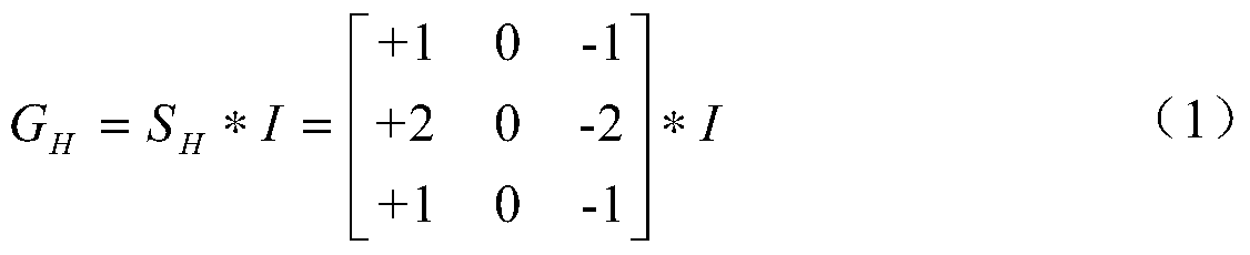
- G H represents a horizontal direction edge image of the template image or the test image
- G V represents a vertical direction edge image of the template image or the test image
- G D represents a diagonal direction edge image of the template image or the test image
- S H represents The horizontal direction convolution kernel
- S V represents the vertical direction convolution kernel
- S D represents the diagonal direction convolution kernel
- I represents the original template image or the test image.
- the template image and the test image respectively obtain edge images in three directions, from the original one original image to three edge images in three directions.
- the original template image and the test image of the socket are first obtained, and the original template image and the test image of the socket are respectively extracted in three directions, and finally the horizontal edge image and the vertical edge image of the template image are obtained.
- the electronic component missing component detecting method of the present invention divides the first edge image and the second edge image separately, and performs each partition of the first edge image and the second edge image.
- Feature extraction, obtaining the first feature parameter of the template image and the second feature parameter of the test image, the step S102 includes:
- Step S1021 dividing the first edge image of the template image in three directions and the second edge image of the test image into a plurality of partitions, respectively;
- the electronic component missing component detecting method of the present invention the step S1021 of dividing the first edge image of the template image in three directions and the second edge image of the test image into a plurality of partitions respectively Can include:
- the first edge image of the template image in the three directions and the second edge image of the test image are respectively divided into four non-overlapping and identically sized partitions.
- the obtained first edge image and the second edge image are respectively divided into four non-overlapping and identically-sized partitions, which effectively preserves the global structural features of the original template image and the test image, which is beneficial for subsequent
- the accuracy of calculating the similarity values of the two steps further ensures the accuracy of the electronic component missing component detection.
- the acquired edge image may also be divided into partitions of different sizes or overlapping each other, and the specific partitioning method may be Adjust according to the actual detection accuracy requirements and other actual needs.
- Step S1022 Calculating local binary eigenvalues of each partition by using a local binary mode method, and combining local binary eigenvalues of each partition of the first edge image and the second edge image in a vector manner to obtain a template image.
- the first characteristic parameter and the second characteristic parameter of the test image are the first characteristic parameter and the second characteristic parameter of the test image.
- the Local Binary Patterns (LBP) described in the above embodiments are non-parametric operators that describe the local spatial structure of an image. It not only accurately describes detailed texture information such as points, lines, edges, but also has The advantages of translation invariance and rotation invariance; but because the local binary pattern feature is represented by a histogram, the histogram is a feature representation with weak resolution, because it is a first-order statistical feature. Ignoring the global structural features of the image, if only one histogram is generated for the entire image, important structural difference information is inevitably lost. Therefore, the electronic component missing component detecting method of the present invention passes the 3 obtained in step S101 in step S1021.
- the edge images in the direction of the strip are divided into a plurality of partitions. In this embodiment, each edge image is divided into four partitions of the same size and not overlapping.
- the edge image in each direction can be equally divided into four partitions, such that the first edge image in three directions of the template image is divided into 12 partitions. Similarly, the second edge image in the three directions of the test image is also divided into 12 partitions.
- the local binary value method is used to calculate the local binary eigenvalues of the 12 partitions of the first edge image and the local binary eigenvalues of the 12 partitions of the second edge image, respectively, in step S1022.
- the local binary eigenvalues of the 12 partitions of an edge image and the local binary eigenvalues of the 12 partitions of the second edge image are respectively combined in a vector manner to obtain a first feature parameter of the template image and a second test image.
- Characteristic Parameters That is, the first feature parameter is a composite vector composed of 12 local binary eigenvalues of the first edge image, and the second feature parameter is a composite vector composed of 12 local binary eigenvalues of the second edge image.
- the electronic component missing component detecting method of the present invention the calculating the similarity value of the template image and the test image according to the first feature parameter and the second feature parameter comprises:
- the electronic component missing component detecting method of the present invention according to the first characteristic parameter And the step of calculating the similarity value between the template image and the test image by the second characteristic parameter and intersecting the histogram includes:
- H1 and H2 represent the characteristic histogram of the first characteristic parameter and the characteristic histogram of the second characteristic parameter, respectively, and B represents the interval length of the histogram.
- the step of performing electronic component missing component detection on the circuit board according to the similarity value comprises:
- the step of determining whether the electronic component on the circuit board is missing according to the magnitude relationship between the similarity value and the preset threshold value comprises:
- the electronic component missing component detection is performed on the circuit board to be tested according to the similarity value between the calculated template image and the test image.
- R represents the similarity value between the template image and the test image
- T represents a preset threshold
- the electronic component missing component detecting method performs three-direction edge image extraction on the template image and the test image of the obtained electronic component's circuit board, so that the obtained edge image contains more detailed information; Separating the image and the second edge image respectively, and performing feature extraction on each of the first edge image and the second edge image to obtain a first feature parameter of the template image and a second feature parameter of the test image; The similarity value calculated by a characteristic parameter and the second characteristic parameter performs electronic component missing component detection on the circuit board.
- FIG. 2 is a schematic structural diagram of an electronic component missing component detecting system according to an embodiment of the present invention, including:
- the edge extraction module 101 is configured to perform edge image extraction on the template image and the test image of the circuit board of the acquired electronic component to obtain a first edge image and a second edge image;
- the edge extraction module 101 obtains the edge image information of the template image and the test image of the acquired electronic component, and obtains the edge detail information of the template image and the test image to ensure that the detection result of the subsequent step is more accurate.
- the feature extraction module 102 is configured to separately partition the first edge image and the second edge image, and perform feature extraction on each partition of the first edge image and the second edge image to obtain a first feature parameter of the template image and Testing a second characteristic parameter of the image;
- the feature extraction module 102 performs segmentation on the first edge image and the second edge image, and performs feature extraction on each partition of the first edge image and the second edge image to obtain a first feature parameter and a test of the template image.
- the second characteristic parameter of the image is used to calculate the similarity value of the template image and the test image in the subsequent steps.
- the similarity calculation module 103 is configured to calculate a similarity value between the template image and the test image according to the first feature parameter and the second feature parameter;
- the similarity values of the two are calculated according to the first feature parameter including the template image feature information and the second feature parameter including the test image, and the electronic circuit to be tested is performed according to the similarity value for the subsequent step.
- Component missing parts detection is performed according to the similarity value for the subsequent step.
- the detecting module 104 is configured to perform electronic component missing component detection on the circuit board according to the similarity value.
- the electronic component missing component detecting system performs edge image extraction on the template image and the test image of the obtained electronic component board by the edge extraction module 101 to obtain edge information of the template image and the test image; and the feature extraction module 102 Separating the first edge image and the second edge image separately, and performing feature extraction on each partition of the first edge image and the second edge image to obtain a first feature parameter of the template image and a second test image
- the feature parameter; the reuse similarity calculation module 103 performs the electronic component missing component detection on the circuit board by using the detection module 104 according to the similarity value calculated by the first feature parameter and the second feature parameter.
- the edge extraction module 101 may also For:
- Edge image extraction is performed on the template image and the test image from three directions, respectively, to obtain a first edge image of the template image in three directions and a second edge image of the test image; wherein the three directions are respectively The horizontal direction, the vertical direction, and the diagonal direction of the template image and the test image.
- the first edge image and the second image in the three directions of the template image and the test image are obtained by performing edge extraction on the horizontal direction, the vertical direction, and the diagonal direction of the template image and the test image, respectively.
- Edge image is ensured that the obtained edge image contains more edge detail information, and the effectiveness of feature extraction on the obtained edge image in the subsequent steps is also ensured.
- the edge extraction module 101 can also be used to perform horizontal, vertical, and opposite directions by the above-described formulas (1) to (3), respectively.
- the edge direction extracts the edge of the template image and the test image.
- the template image and the test image respectively obtain edge images in three directions, from the original one original image to the edge image in three directions.
- FIG. 3 is a schematic structural diagram of a feature extraction module of an electronic component missing component detecting system according to another embodiment of the present invention, including:
- the partitioning module 1021 is configured to divide the first edge image of the template image in three directions and the second edge image of the test image into a plurality of partitions, respectively.
- the partitioning module 1021 can also be used to:
- the first edge image of the template image in the three directions and the second edge image of the test image are respectively divided into four non-overlapping and identically sized partitions.
- the obtained first edge image and the second edge image are respectively divided into four non-overlapping and identically-sized partitions, which effectively preserves the global structural features of the original template image and the test image, which is beneficial for subsequent
- the accuracy of calculating the similarity values of the two steps further ensures the accuracy of the electronic component missing component detection.
- the acquired edge image may also be divided into partitions of different sizes or overlapping each other, and the specific partitioning method may be adjusted according to actual detection accuracy requirements and other actual requirements.
- the feature parameter calculation module 1022 is configured to calculate a local binary eigenvalue of each partition by using a local binary mode method, and combine the local binary eigenvalues of each partition of the first edge image and the second edge image in a vector manner respectively. Obtaining a first feature parameter of the template image and a second feature parameter of the test image.
- the Local Binary Patterns (LBP) described in the above embodiments are non-parametric operators that describe the local spatial structure of an image. It not only accurately describes detailed texture information such as points, lines, edges, but also has The advantages of translation invariance and rotation invariance; but because the local binary pattern feature is represented by a histogram, the histogram is a feature representation with weak resolution, because it is a first-order statistical feature. Ignoring the global structural features of the image, if only one histogram is generated for the entire image, important structural difference information is inevitably lost. Therefore, the electronic component missing component detecting method of the present invention obtains the edge extraction module 101 by the partitioning module 1021.
- the edge images in the three directions are each divided into a plurality of partitions. In this embodiment, each edge image is divided into four partitions of the same size and not overlapping.
- the edge image in each direction can be equally divided into four partitions, such that the first edge image in three directions of the template image is divided into 12 partitions. Similarly, the second edge image in the three directions of the test image is also divided into 12 partitions.
- the feature parameter calculating module 1022 respectively calculates the local binary value of the 12 partitions of the first edge image and the local binary features of the 12 partitions of the second edge image by using the local binary pattern method. And combining the local binary eigenvalues of the 12 partitions of the first edge image and the local binary eigenvalues of the 12 partitions of the second edge image in a vector manner to obtain the first characteristic parameter of the template image and The second characteristic parameter of the test image. That is, the first feature parameter is a composite vector composed of 12 local binary eigenvalues of the first edge image, and the second feature parameter is a composite vector composed of 12 local binary eigenvalues of the second edge image.
- the electronic component missing component detecting system of the present invention is configured to:
- the electronic component missing component detecting system of the present invention can also be used to:
- H1 and H2 represent the characteristic histogram of the first characteristic parameter and the characteristic histogram of the second characteristic parameter, respectively, and B represents the interval length of the histogram.
- the electronic component missing component detecting system of the present invention is further configured to:
- the first edge image and the second edge image in the three directions of the template image and the test image are respectively divided into four partitions that are not overlapping and the same size.
- the electronic component missing component detecting system of the present invention can also be used to:
- the electronic component missing component detecting system of the present invention can also be used to:
- the electronic component missing component detection is performed on the circuit board to be tested according to the similarity value between the calculated template image and the test image.
- R represents the similarity value between the template image and the test image
- T represents a preset threshold
- the electronic component missing component detecting method and system respectively perform edge image extraction in three directions on a template image and a test image of a circuit board of the acquired electronic component, so that the obtained edge image contains more detailed information;
- the first edge image and the second edge image are respectively partitioned, and feature extraction of the local binary pattern is performed on each partition of the first edge image and the second edge image, so that the obtained feature parameter includes more global structural features.
Landscapes
- Physics & Mathematics (AREA)
- General Physics & Mathematics (AREA)
- Engineering & Computer Science (AREA)
- Biochemistry (AREA)
- Immunology (AREA)
- Life Sciences & Earth Sciences (AREA)
- Chemical & Material Sciences (AREA)
- Analytical Chemistry (AREA)
- Pathology (AREA)
- General Health & Medical Sciences (AREA)
- Health & Medical Sciences (AREA)
- Computer Vision & Pattern Recognition (AREA)
- Theoretical Computer Science (AREA)
- Image Analysis (AREA)
- Signal Processing (AREA)
- Quality & Reliability (AREA)
- Image Processing (AREA)
Abstract
一种电子元件漏件检测方法和系统,其中,所述方法包括如下步骤:对获取的电子元件的电路板的模板图像和测试图像分别进行边缘图像提取,得到第一边缘图像和第二边缘图像(S101);对所述第一边缘图像和第二边缘图像分别进行分区,并对各个分区上的第一边缘图像和第二边缘图像进行特征提取,得到模板图像的第一特征参数和测试图像的第二特征参数(S102);根据第一特征参数和第二特征参数计算所述模板图像与测试图像的相似度值(S103);根据所述相似度值对电路板进行电子元件漏件检测(S104)。该方法和系统,通过有效地提高了电子元件漏件检测的准确率,保证了检测后的电路板的质量。
Description
本发明涉及光学检测技术领域,特别是涉及一种电子元件漏件检测方法和系统。
光学检测是工业制作过程的必要环节,利用光学方式取得成品的表面状态,以影像处理来检测异物或表面瑕疵。电子元件的错、漏、反检测是电路板缺陷检测领域中的一种常见应用,机器通过摄像头自动扫描电路板获取图像,提取每个电子元件的局部图像,来判断电子元件是否存在错、漏、反缺陷,最后将疑似缺陷的元件显示或标记出来,方便查看与检修。
电子元件的漏件检测是指判断电子元件是否插在指定的位置上,如果没有插在指定的位置上,则判为漏件;如果插在指定的位置上,则判为正常。
在传统的自动光学检测系统中,电子元件的漏件检测主要是通过以下两种方法来实现:
方法一、颜色对比法,即通过对比对应位置的像素颜色值的差别来对电路板进行电子元件漏件检测;方法二、深度学习模型判别法,即通过准备大量的电子元件的样本(包括正样本:电子元件存在;负样本:电子元件不存在)对深度学习模型进行训练来对电子元件的漏件进行检测,但是,现有的技术方案仍然存在如下的问题:
针对方法一,传统的颜色对比法,比较容易受到光照变化的影响,使电子元件的颜色信息发生变化,从而产生误判;针对方法二,深度学习模型判别法,需要大量的训练样本,一般情况下,无法获得覆盖所有电子元件的训练样本,而只基于部分样本训练的深度学习的漏件检测模型,也容易发生误判。
综上所述,现有的电子元件漏检方法的误判率较高,无法保证检测后的电路板的质量。
发明内容
基于此,有必要针对现有的电子元件漏检方法的误判率较高的技术问题,提供一种电子元件漏件检测方法。
一种电子元件漏件检测方法,包括如下步骤:
对获取的电子元件的电路板的模板图像和测试图像分别进行边缘图像提取,得到第一边缘图像和第二边缘图像;
对所述第一边缘图像和第二边缘图像分别进行分区,并对各个分区上的第一边缘图像和第二边缘图像进行特征提取,得到模板图像的第一特征参数和测试图像的第二特征参数;
根据第一特征参数和第二特征参数计算所述模板图像与测试图像的相似度值;
根据所述相似度值对电路板进行电子元件漏件检测。
上述电子元件漏件检测方法,通过对获取的电子元件的电路板的模板图像和测试图像分别进行边缘图像提取,获取所述模板图像和测试图像的边缘图像信息;通过对第一边缘图像和第二边缘图像分别进行分区,并对第一边缘图像和第二边缘图像的各个分区进行特征提取,获取第一边缘图像和第二边缘图像包含的全局结构特征信息;再根据第一特征参数和第二特征参数计算得到的相似度值对电路板进行电子元件漏件检测。通过上述技术方案,有效地提高了电路板电子元件漏件检测的准确率,保证了检测后的电路板的质量。
一种电子元件漏件检测系统,包括:
边缘提取模块,用于对获取的电子元件的电路板的模板图像和测试图像分别进行边缘图像提取,得到第一边缘图像和第二边缘图像;
特征提取模块,用于对所述第一边缘图像和第二边缘图像分别进行分区,并对第一边缘图像和第二边缘图像的各个分区进行特征提取,得到模板图像的第一特征参数和测试图像的第二特征参数;
相似度计算模块,用于根据第一特征参数和第二特征参数计算所述模板图像与测试图像的相似度值;
检测模块,用于根据所述相似度值对电路板进行电子元件漏件检测。
上述电子元件漏件检测系统,通过边缘提取模块对获取的电子元件的电路板的模板图像和测试图像分别进行边缘图像提取,获取所述模板图像和测试图像的边缘信息;通过特征提取模块对所述第一边缘图像和第二边缘图像分别进行分区,并对第一边缘图像和第二边缘图像的各个分区进行特征提取,得到所述模板图像的第一特征参数和测试图像的第二特征参数;再利用相似度计算模块根据第一特征参数和第二特征参数计算得到的相似度
值,利用检测模块对电路板进行电子元件漏件检测。通过上述技术方案,有效地提高了电路板电子元件漏件检测的准确率,保证了检测后的电路板的质量。
图1为本发明的一个实施例的电子元件漏件检测方法流程图;
图2为本发明的一个实施例的电子元件漏件检测系统的结构示意图;
图3为本发明的另一个实施例的电子元件漏件检测系统的特征提取模块的结构示意图。
为了更进一步阐述本发明所采取的技术手段及取得的效果,下面结合附图及较佳实施例,对本发明的技术方案,进行清楚和完整的描述。
如图1所示,图1为本发明的一个实施例的电子元件漏件检测方法流程图,包括如下步骤:
步骤S101:对获取的电子元件的电路板的模板图像和测试图像分别进行边缘图像提取,得到第一边缘图像和第二边缘图像;
在本步骤中,通过对获取的电子元件的电路板的模板图像和测试图像分别进行边缘图像提取,获取所述模板图像和测试图像的边缘细节信息,确保后续步骤的检测结果更准确。
步骤S102:对所述第一边缘图像和第二边缘图像分别进行分区,并对第一边缘图像和第二边缘图像的各个分区进行特征提取,得到模板图像的第一特征参数和测试图像的第二特征参数;
在本步骤中,通过对所述第一边缘图像和第二边缘图像分别进行分区,并对第一边缘图像和第二边缘图像的各个分区进行特征提取,得到模板图像的第一特征参数和测试图像的第二特征参数,用于后续步骤的计算模板图像和测试图像的相似度值。
步骤S103:根据第一特征参数和第二特征参数计算模板图像与测试图像的相似度值;
在本步骤中,根据包含模板图像特征信息的第一特征参数和包含测试图像的第二特征参数计算两者的相似度值,用于后续步骤的根据所述相似度值对待测电路板进行电子元件漏件检测。
步骤S104:根据所述相似度值对电路板进行电子元件漏件检测。
上述电子元件漏件检测方法,通过对获取的电子元件的电路板的模板图像和测试图像分别进行边缘图像提取,获取所述模板图像和测试图像的边缘图像信息;通过对第一边缘图像和第二边缘图像分别进行分区,并对第一边缘图像和第二边缘图像的各个分区进行特征提取,得到所述模板图像的第一特征参数和测试图像的第二特征参数;再根据第一特征参数和第二特征参数计算得到的相似度值对电路板进行电子元件漏件检测。通过上述技术方案,有效地提高了电路板电子元件漏件检测的准确率,保证了检测后的电路板的质量。
在实际的电子元件漏件检测的一种重要信息就是电子元件本身的边缘信息,不同电子元件的边缘结构也是不一样的,漏插电子元件之后的电路板的图片的边缘信息和插了电子元件的电路板的图像的边缘信息也是不一样的。因此,可以根据获取的待测电路板的模板图像和测试图像的边缘信息来对待测电路板进行电子元件漏件检测。
在其中一个实施例中,本发明的电子元件漏件检测方法,所述对获取的电子元件的电路板的模板图像和测试图像分别进行边缘图像提取,得到第一边缘图像和第二边缘图像的步骤S101包括:
从三个方向上分别对所述模板图像和测试图像进行边缘图像提取,得到三个方向上的模板图像的第一边缘图像和测试图像的第二边缘图像;其中,所述三个方向分别为所述模板图像和测试图像的水平方向、垂直方向和对角线方向。
在上述实施例中,通过对上述模板图像和测试图像的水平方向、垂直方向和对角线方向分别进行边缘提取,得到上述模板图像和测试图像的三个方向上的第一边缘图像和第二边缘图像。通过上述技术方案,确保获得的边缘图像包含更多的边缘细节信息,也确保了后续步骤的对得到的边缘图像进行特征提取的有效性。
在其中一个实施例中,本发明的电子元件漏件检测方法,所述从三个方向上分别对所述模板图像和测试图像进行边缘图像提取,得到三个方向上的模板图像的第一边缘图像和测试图像的第二边缘图像的步骤可以包括:


式中,GH表示模板图像或测试图像的水平方向边缘图像,GV表示模板图像或测试图像的垂直方向边缘图像,GD表示模板图像或测试图像的对角线方向边缘图像,SH表示水平方向卷积核,SV表示垂直方向卷积核,SD表示对角线方向卷积核,I表示原始模板图像或测试图像。
通过上述处理,所述模板图像和测试图像分别获得了三个方向的边缘图像,从原来的一张原始图像变成了三张三个方向上的边缘图像。以插座为例,首先获取插座的原始模板图像和测试图像,分别对插座的原始模板图像和测试图像进行三个方向上的边缘提取,最终得到模板图像的水平方向边缘图像、垂直方向边缘图像和对角线方向边缘图像以及测试图像的水平方向边缘图像、垂直方向边缘图像和对角线方向边缘图像。
在其中一个实施例中,本发明的电子元件漏件检测方法,所述对所述第一边缘图像和第二边缘图像分别进行分区,并对第一边缘图像和第二边缘图像的各个分区进行特征提取,得到模板图像的第一特征参数和测试图像的第二特征参数的步骤S102包括:
步骤S1021:将三个方向上的模板图像的第一边缘图像和测试图像的第二边缘图像分别划分成若干个分区;
在其中一个实施例中,本发明的电子元件漏件检测方法,所述将三个方向上的模板图像的第一边缘图像和测试图像的第二边缘图像分别划分成若干个分区的步骤S1021还可以包括:
将三个方向上的模板图像的第一边缘图像和测试图像的第二边缘图像分别划分成四个不相重叠且大小相同的分区。
在本实施例中,将得到的第一边缘图像和第二边缘图像分别划分为四个不相重叠且大小相同的分区,有效地保留了原始模板图像和测试图像的全局结构特征,有利于后续步骤的计算两者的相似度值的准确度,也进一步保证了电子元件漏件检测的准确率。在实际应用中,也可以将获取的边缘图像划分为大小不等或者相互重叠的分区,具体的分区方法可
以根据实际的检测精度要求以及其他实际需求进行调整。
步骤S1022:利用局部二值模式方法计算各个分区的局部二值特征值,分别将第一边缘图像和第二边缘图像的各个分区的局部二值特征值以向量的方式进行组合,得到模板图像的第一特征参数和测试图像的第二特征参数。
上述实施例中所述的局部二值模式(Local Binary Patterns,LBP)是一种描述图像局部空间结构的非参数算子,它不仅能够准确描述点、线、边缘等细节纹理信息,而且还具有平移不变性、旋转不变性的优点;但是因为局部二值模式特征是利用直方图进行表示的,而直方图是一种分辨能力较弱的特征表示方法,因为它是一种一阶统计特征,忽略了图像的全局结构特征,如果对整张图像只生成一个直方图,必然会丢失重要的结构差异信息,因此,本发明的电子元件漏件检测方法通过在步骤S1021中将步骤S101获得的3张带方向的边缘图像,各自地划分为若干个分区,在本实施例中,将各个边缘图像分别划分为四个大小相同且不相重叠的分区。
在实际应用中,需要对得到的模板图像的水平方向边缘图像、垂直方向边缘图像和对角线方向边缘图像以及测试图像的水平方向边缘图像、垂直方向边缘图像和对角线方向边缘图像分别进行分区。作为一种实施方式,可以将每一方向上的边缘图像均分为四个分区,这样,模板图像的三个方向上的第一边缘图像就被分为12个分区。同样地,测试图像的三个方向上的第二边缘图像也被分为12个分区。
完成上述分区之后,在步骤S1022中利用局部二值模式方法分别计算第一边缘图像的12个分区的局部二值特征值和第二边缘图像的12个分区的局部二值特征值,再将第一边缘图像的12个分区的局部二值特征值和第二边缘图像的12个分区的局部二值特征值分别以向量的方式组合起来,得到模板图像的第一特征参数和测试图像的第二特征参数。也就是说,第一特征参数是由第一边缘图像的12个局部二值特征值组成的复合向量,第二特征参数是由第二边缘图像的12个局部二值特征值组成的复合向量。
在其中一个实施例中,本发明的电子元件漏件检测方法,所述根据第一特征参数和第二特征参数计算所述模板图像与测试图像的相似度值的步骤包括:
根据所述第一特征参数和第二特征参数,并按照直方图相交的方式计算所述模板图像与测试图像的相似度值。
在其中一个实施例中,本发明的电子元件漏件检测方法,所述根据所述第一特征参数
和第二特征参数,并按照直方图相交的方式计算所述模板图像与测试图像的相似度值的步骤包括:

式中,D(H1,H2)表示模板图像和测试图像的相似度值,H1和H2分别表示第一特征参数的特征直方图和第二特征参数的特征直方图,B表示直方图的区间长度。
在其中一个实施例中,本发明的电子元件漏件检测方法,所述根据所述相似度值对电路板进行电子元件漏件检测的步骤包括:
将所述相似度值与预设阈值进行比较,根据所述相似度值与预设阈值的大小关系,判断电路板的电子元件是否漏件。
在其中一个实施例中,本发明的电子元件漏件检测方法,所述根据所述相似度值与预设阈值的大小关系,判断电路板上的电子元件是否漏件的步骤包括:
若所述相似度值不小于设定阈值,则判定电路板的电子元件漏件;
若所述相似度值小于设定阈值,则判定电路板的电子元件正常。
在上述实施例中,根据计算的模板图像和测试图像之间的相似度值来对待测电路板进行电子元件漏件检测,具体地,两者之间的相似度值越小,表示二者之间越相似;在实际应用时,我们也可以通过定义R=1-D;其中,D为根据上述方法获得的二者的相似度值,将其转换为相似度值R越大越相似。即,重新定义后的判断方法如下式所示:

式中,R表示模板图像和测试图像之间的相似度值,T表示预设阈值。
上述电子元件漏件检测方法,通过对获取的电子元件的电路板的模板图像和测试图像分别进行三个方向的边缘图像提取,使得得到的边缘图像包含更多的细节信息;通过对第一边缘图像和第二边缘图像分别进行分区,并对第一边缘图像和第二边缘图像的各个分区进行特征提取,得到所述模板图像的第一特征参数和测试图像的第二特征参数;再根据第一特征参数和第二特征参数计算得到的相似度值对电路板进行电子元件漏件检测。通过上述技术方案,有效地提高了电路板电子元件漏件检测的准确率,保证了检测后的电路板的
质量。
如图2所示,图2为本发明的一个实施例的电子元件漏件检测系统的结构示意图,包括:
边缘提取模块101,用于对获取的电子元件的电路板的模板图像和测试图像分别进行边缘图像提取,得到第一边缘图像和第二边缘图像;
上述边缘提取模块101通过对获取的电子元件的电路板的模板图像和测试图像分别进行边缘图像提取,获取所述模板图像和测试图像的边缘细节信息,确保后续步骤的检测结果更准确。
特征提取模块102,用于对所述第一边缘图像和第二边缘图像分别进行分区,并对第一边缘图像和第二边缘图像的各个分区进行特征提取,得到模板图像的第一特征参数和测试图像的第二特征参数;
上述特征提取模块102通过对所述第一边缘图像和第二边缘图像分别进行分区,并对第一边缘图像和第二边缘图像的各个分区进行特征提取,得到模板图像的第一特征参数和测试图像的第二特征参数,用于后续步骤的计算模板图像和测试图像的相似度值。
相似度计算模块103,用于根据第一特征参数和第二特征参数计算所述模板图像与测试图像的相似度值;
在本步骤中,根据包含模板图像特征信息的第一特征参数和包含测试图像的第二特征参数计算两者的相似度值,用于后续步骤的根据所述相似度值对待测电路板进行电子元件漏件检测。
检测模块104,用于根据所述相似度值对电路板进行电子元件漏件检测。
上述电子元件漏件检测系统,通过边缘提取模块101对获取的电子元件的电路板的模板图像和测试图像分别进行边缘图像提取,获取所述模板图像和测试图像的边缘信息;通过特征提取模块102对所述第一边缘图像和第二边缘图像分别进行分区,并对第一边缘图像和第二边缘图像的各个分区进行特征提取,得到所述模板图像的第一特征参数和测试图像的第二特征参数;再利用相似度计算模块103根据第一特征参数和第二特征参数计算得到的相似度值,利用检测模块104对电路板进行电子元件漏件检测。通过上述技术方案,有效地提高了电路板电子元件漏件检测的准确率,保证了检测后的电路板的质量。
在其中一个实施例中,本发明的电子元件漏件检测系统,所述边缘提取模块101还可
以用于:
从三个方向上分别对所述模板图像和测试图像进行边缘图像提取,得到三个方向上的模板图像的第一边缘图像和测试图像的第二边缘图像;其中,所述三个方向分别为所述模板图像和测试图像的水平方向、垂直方向和对角线方向。
在上述实施例中,通过对上述模板图像和测试图像的水平方向、垂直方向和对角线方向分别进行边缘提取,得到上述模板图像和测试图像的三个方向上的第一边缘图像和第二边缘图像。通过上述技术方案,确保获得的边缘图像包含更多的边缘细节信息,也确保了后续步骤的对得到的边缘图像进行特征提取的有效性。
在其中一个实施例中,本发明的电子元件漏件检测系统,所述边缘提取模块101还可以用于,通过前面所述的式(1)~(3)分别从水平方向、垂直方向和对角线方向对模板图像和测试图像进行边缘提取。通过上述处理,所述模板图像和测试图像分别获得了三个方向的边缘图像,从原来的一张原始图像变成了三个方向上的边缘图像。
如图3所示,图3为本发明的另一个实施例的电子元件漏件检测系统的特征提取模块的结构示意图,包括:
分区模块1021,用于将三个方向上的模板图像的第一边缘图像和测试图像的第二边缘图像分别划分成若干个分区。
在其中一个实施例中,本发明的电子元件漏件检测系统,所述分区模块1021还可以用于:
将三个方向上的模板图像的第一边缘图像和测试图像的第二边缘图像分别划分成四个不相重叠且大小相同的分区。
在本实施例中,将得到的第一边缘图像和第二边缘图像分别划分为四个不相重叠且大小相同的分区,有效地保留了原模板图像和测试图像的全局结构特征,有利于后续步骤的计算两者的相似度值的准确度,也进一步保证了电子元件漏件检测的准确率。在实际应用中,也可以将获取的边缘图像划分为大小不等或者相互重叠的分区,具体的分区方法可以根据实际的检测精度要求以及其他实际需求进行调整。
特征参数计算模块1022,用于利用局部二值模式方法计算各个分区的局部二值特征值,分别将第一边缘图像和第二边缘图像的各个分区的局部二值特征值以向量的方式进行组合,得到模板图像的第一特征参数和测试图像的第二特征参数。
上述实施例中所述的局部二值模式(Local Binary Patterns,LBP)是一种描述图像局部空间结构的非参数算子,它不仅能够准确描述点、线、边缘等细节纹理信息,而且还具有平移不变性、旋转不变性的优点;但是因为局部二值模式特征是利用直方图进行表示的,而直方图是一种分辨能力较弱的特征表示方法,因为它是一种一阶统计特征,忽略了图像的全局结构特征,如果对整张图像只生成一个直方图,必然会丢失重要的结构差异信息,因此,本发明的电子元件漏件检测方法通过分区模块1021将边缘提取模块101获得的3个方向上的边缘图像,各自地划分为若干个分区,在本实施例中,将各个边缘图像分别划分为四个大小相同且不相重叠的分区。
在实际应用中,需要对得到的模板图像的水平方向边缘图像、垂直方向边缘图像和对角线方向边缘图像以及测试图像的水平方向边缘图像、垂直方向边缘图像和对角线方向边缘图像分别进行分区。作为一种实施方式,可以将每一方向上的边缘图像均分为四个分区,这样,模板图像的三个方向上的第一边缘图像就被分为12个分区。同样地,测试图像的三个方向上的第二边缘图像也被分为12个分区。
分区模块1021在完成上述分区之后,特征参数计算模块1022利用局部二值模式方法分别计算第一边缘图像的12个分区的局部二值特征值和第二边缘图像的12个分区的局部二值特征值,再将第一边缘图像的12个分区的局部二值特征值和第二边缘图像的12个分区的局部二值特征值分别以向量的方式组合起来,得到模板图像的第一特征参数和测试图像的第二特征参数。也就是说,第一特征参数是由第一边缘图像的12个局部二值特征值组成的复合向量,第二特征参数是由第二边缘图像的12个局部二值特征值组成的复合向量。
在其中一个实施例中,本发明的电子元件漏件检测系统,所述相似度计算模块103用于:
根据所述第一特征参数和第二特征参数,并按照直方图相交的方式计算所述模板图像与测试图像的相似度值。
在其中一个实施例中,本发明的电子元件漏件检测系统,所述相似度计算模块103还可以用于:

式中,D(H1,H2)表示模板图像和测试图像的相似度值,H1和H2分别表示第一特征参数的特征直方图和第二特征参数的特征直方图,B表示直方图的区间长度。
在其中一个实施例中,本发明的电子元件漏件检测系统,所述特征提取模块102还用于:
将所述模板图像和测试图像的三个方向上的第一边缘图像和第二边缘图像分别划分成四个不相重叠且大小相同的分区。
在其中一个实施例中,本发明的电子元件漏件检测系统,所述检测模块104还可以用于:
将所述相似度值与预设阈值进行比较,根据所述相似度值与预设阈值的大小关系,判断电路板的电子元件是否漏件。
在其中一个实施例中,本发明的电子元件漏件检测系统,所述检测模块104还可以用于:
若所述相似度值不小于设定阈值,则判定电路板的电子元件漏件;
若所述相似度值小于设定阈值,则判定电路板的电子元件正常。
在上述实施例中,根据计算的模板图像和测试图像之间的相似度值来对待测电路板进行电子元件漏件检测,具体地,两者之间的相似度值越小,表示二者之间越相似;在实际应用时,我们也可以通过定义R=1-D;其中,D为根据上述方法获得的二者的相似度值,将其转换为相似度值R越大越相似。即,重新定义后的判断方法如下式所示:

式中,R表示模板图像和测试图像之间的相似度值,T表示预设阈值。
上述电子元件漏件检测方法和系统,通过对获取的电子元件的电路板的模板图像和测试图像分别进行三个方向的边缘图像提取,使得得到的边缘图像包含更多的细节信息;通过对所述第一边缘图像和第二边缘图像分别进行分区,并对第一边缘图像和第二边缘图像的各个分区进行局部二值模式的特征提取,使得得到的特征参数包含更多的全局结构特征
信息;再根据第一特征参数和第二特征参数计算所述模板图像与测试图像的相似度值,并根据所述相似度值对电路板进行电子元件漏件检测。通过上述技术方案,有效地提高了电子元件漏件检测的准确率,保证了检测后的电路板的质量。
以上所述实施例的各技术特征可以进行任意的组合,为使描述简洁,未对上述实施例中的各个技术特征所有可能的组合都进行描述,然而,只要这些技术特征的组合不存在矛盾,都应当认为是本说明书记载的范围。
以上所述实施例仅表达了本发明的几种实施方式,其描述较为具体和详细,但并不能因此而理解为对发明专利范围的限制。应当指出的是,对于本领域的普通技术人员来说,在不脱离本发明构思的前提下,还可以做出若干变形和改进,这些都属于本发明的保护范围。因此,本发明专利的保护范围应以所附权利要求为准。
Claims (10)
- 一种电子元件漏件检测方法,其特征在于,包括如下步骤:对获取的电子元件的电路板的模板图像和测试图像分别进行边缘图像提取,得到第一边缘图像和第二边缘图像;对所述第一边缘图像和第二边缘图像分别进行分区,并对第一边缘图像和第二边缘图像的各个分区进行特征提取,得到模板图像的第一特征参数和测试图像的第二特征参数;根据第一特征参数和第二特征参数计算所述模板图像与测试图像的相似度值;根据所述相似度值对电路板进行电子元件漏件检测。
- 根据权利要求1所述的电子元件漏件检测方法,其特征在于,所述对获取的电子元件的电路板的模板图像和测试图像分别进行边缘图像提取,得到第一边缘图像和第二边缘图像的步骤包括:从三个方向上分别对所述模板图像和测试图像进行边缘图像提取,得到三个方向上的模板图像的第一边缘图像和测试图像的第二边缘图像;其中,所述三个方向分别为所述模板图像和测试图像的水平方向、垂直方向和对角线方向。
- 根据权利要求2所述的电子元件漏件检测方法,其特征在于,所述从三个方向上分别对所述模板图像和测试图像进行边缘图像提取,得到三个方向上的模板图像的第一边缘图像和测试图像的第二边缘图像的步骤包括:

 式中,GH表示模板图像或测试图像的水平方向边缘图像,GV表示模板图像或测试图像的垂直方向边缘图像,GD表示模板图像或测试图像的对角线方向边缘图像,SH表示水 平方向卷积核,SV表示垂直方向卷积核,SD表示对角线方向卷积核,I表示原始模板图像或测试图像。
 - 根据权利要求2所述的电子元件漏件检测方法,其特征在于,所述对所述第一边缘图像和第二边缘图像分别进行分区,并对各个分区上的第一边缘图像和第二边缘图像进行特征提取,得到模板图像的第一特征参数和测试图像的第二特征参数的步骤包括:将三个方向上的模板图像的第一边缘图像和测试图像的第二边缘图像分别划分成若干个分区;利用局部二值模式方法计算各个分区的局部二值特征值,分别将第一边缘图像和第二边缘图像的各个分区的局部二值特征值以向量的方式进行组合,得到模板图像的第一特征参数和测试图像的第二特征参数。
- 根据权利要求3所述的电子元件漏件检测方法,其特征在于,所述根据第一特征参数和第二特征参数计算所述模板图像与测试图像的相似度值的步骤包括:根据所述第一特征参数和第二特征参数,并按照直方图相交的方式计算所述模板图像与测试图像的相似度值。
- 根据权利要求5所述的电子元件漏件检测方法,其特征在于,所述根据所述第一特征参数和第二特征参数,并按照直方图相交的方式计算所述模板图像与测试图像的相似度值的步骤包括:
 式中,D(H1,H2)表示模板图像和测试图像的相似度值,H1和H2分别表示第一特征参数的特征直方图和第二特征参数的特征直方图,B表示特征直方图的区间长度。
 - 根据权利要求4所述的电子元件漏件检测方法,其特征在于,所述将三个方向上的模板图像的第一边缘图像和测试图像的第二边缘图像分别划分成若干个分区的步骤包括:将三个方向上的模板图像的第一边缘图像和测试图像的第二边缘图像分别划分成四个不相重叠且大小相同的分区。
- 根据权利要求1所述的电子元件漏件检测方法,其特征在于,所述根据所述相似 度值对电路板进行电子元件漏件检测的步骤包括:将所述相似度值与预设阈值进行比较,根据所述相似度值与预设阈值的大小关系,判断电路板的电子元件是否漏件。
- 根据权利要求8所述的电子元件漏件检测方法,其特征在于,所述根据所述相似度值与预设阈值的大小关系,判断电路板上的电子元件是否漏件的步骤包括:若所述相似度值不小于设定阈值,则判定电路板的电子元件漏件;若所述相似度值小于设定阈值,则判定电路板的电子元件正常。
- 一种电子元件漏件检测系统,其特征在于,包括:边缘提取模块,用于对获取的电子元件的电路板的模板图像和测试图像分别进行边缘图像提取,得到第一边缘图像和第二边缘图像;特征提取模块,用于对所述第一边缘图像和第二边缘图像分别进行分区,并对第一边缘图像和第二边缘图像的各个分区进行特征提取,得到模板图像的第一特征参数和测试图像的第二特征参数;相似度计算模块,用于根据第一特征参数和第二特征参数计算所述模板图像与测试图像的相似度值;检测模块,用于根据所述相似度值对电路板进行电子元件漏件检测。
Applications Claiming Priority (2)
| Application Number | Priority Date | Filing Date | Title |
|---|---|---|---|
| CN201610251817.5A CN105957059B (zh) | 2016-04-20 | 2016-04-20 | 电子元件漏件检测方法和系统 |
| CN201610251817.5 | 2016-04-20 |
Publications (1)
| Publication Number | Publication Date |
|---|---|
| WO2017181724A1 true WO2017181724A1 (zh) | 2017-10-26 |
Family
ID=56917867
Family Applications (1)
| Application Number | Title | Priority Date | Filing Date |
|---|---|---|---|
| PCT/CN2016/112888 Ceased WO2017181724A1 (zh) | 2016-04-20 | 2016-12-29 | 电子元件漏件检测方法和系统 |
Country Status (2)
| Country | Link |
|---|---|
| CN (1) | CN105957059B (zh) |
| WO (1) | WO2017181724A1 (zh) |
Cited By (1)
| Publication number | Priority date | Publication date | Assignee | Title |
|---|---|---|---|---|
| CN115331085A (zh) * | 2022-08-15 | 2022-11-11 | 哈尔滨市科佳通用机电股份有限公司 | 基于深度学习的转向架弹簧托板检测方法 |
Families Citing this family (13)
| Publication number | Priority date | Publication date | Assignee | Title |
|---|---|---|---|---|
| CN105957059B (zh) * | 2016-04-20 | 2019-03-01 | 广州视源电子科技股份有限公司 | 电子元件漏件检测方法和系统 |
| CN106530275B (zh) * | 2016-10-11 | 2019-06-11 | 广州视源电子科技股份有限公司 | 元件错件检测方法和系统 |
| CN106504231A (zh) * | 2016-10-11 | 2017-03-15 | 广州视源电子科技股份有限公司 | 元件缺陷检测方法和系统 |
| CN106525876A (zh) * | 2016-12-30 | 2017-03-22 | 杭州耕德电子有限公司 | 模切件自动漏件检测系统及方法 |
| CN107093174B (zh) * | 2017-04-05 | 2018-03-27 | 湖北工业大学 | 一种pcb设计缺陷检测方法 |
| CN107292901B (zh) * | 2017-07-24 | 2020-06-02 | 北京小米移动软件有限公司 | 边缘检测方法及装置 |
| CN110111293B (zh) * | 2018-01-29 | 2021-05-11 | 国科赛思(北京)科技有限公司 | 塑封器件的失效识别方法及装置 |
| CN108489996B (zh) * | 2018-02-11 | 2020-09-29 | 深圳市朗驰欣创科技股份有限公司 | 一种绝缘子的缺陷检测方法、系统及终端设备 |
| CN109858618B (zh) * | 2019-03-07 | 2020-04-14 | 电子科技大学 | 一种卷积神经单元块、构成的神经网络及图像分类方法 |
| CN113808067B (zh) * | 2020-06-11 | 2024-07-05 | 广东美的白色家电技术创新中心有限公司 | 电路板检测方法、视觉检测设备及具有存储功能的装置 |
| CN113298793B (zh) * | 2021-06-03 | 2023-11-24 | 中国电子科技集团公司第十四研究所 | 一种基于多视角模板匹配的电路板表面缺陷检测的方法 |
| CN116152251B (zh) * | 2023-04-20 | 2023-07-14 | 成都数之联科技股份有限公司 | 电视机背板检测方法、模型训练方法、装置、设备和介质 |
| CN117011369B (zh) * | 2023-08-15 | 2024-11-12 | 合肥图迅电子科技有限公司 | 一种芯片基准点定位方法、装置、计算机设备及存储介质 |
Citations (6)
| Publication number | Priority date | Publication date | Assignee | Title |
|---|---|---|---|---|
| US6163620A (en) * | 1998-05-29 | 2000-12-19 | Eastman Kodak Company | Automatic process for detecting changes between two images |
| CN102289825A (zh) * | 2011-07-08 | 2011-12-21 | 暨南大学 | 一种实时图像边缘检测电路及其实现方法 |
| CN102937595A (zh) * | 2012-11-13 | 2013-02-20 | 浙江省电力公司电力科学研究院 | 一种pcb板检测方法、装置及系统 |
| CN103473537A (zh) * | 2013-09-17 | 2013-12-25 | 湖北工程学院 | 一种目标图像轮廓特征表示方法及装置 |
| CN103544495A (zh) * | 2012-07-12 | 2014-01-29 | 浙江大华技术股份有限公司 | 一种识别图像类别的方法及系统 |
| CN105957059A (zh) * | 2016-04-20 | 2016-09-21 | 广州视源电子科技股份有限公司 | 电子元件漏件检测方法和系统 |
Family Cites Families (2)
| Publication number | Priority date | Publication date | Assignee | Title |
|---|---|---|---|---|
| CN104794472A (zh) * | 2014-01-20 | 2015-07-22 | 富士通株式会社 | 用于提取手势边缘图像的方法和装置以及手势提取方法 |
| CN104809732B (zh) * | 2015-05-07 | 2017-06-20 | 山东鲁能智能技术有限公司 | 一种基于图像比对的电力设备外观异常检测方法 |
-
2016
- 2016-04-20 CN CN201610251817.5A patent/CN105957059B/zh active Active
- 2016-12-29 WO PCT/CN2016/112888 patent/WO2017181724A1/zh not_active Ceased
Patent Citations (6)
| Publication number | Priority date | Publication date | Assignee | Title |
|---|---|---|---|---|
| US6163620A (en) * | 1998-05-29 | 2000-12-19 | Eastman Kodak Company | Automatic process for detecting changes between two images |
| CN102289825A (zh) * | 2011-07-08 | 2011-12-21 | 暨南大学 | 一种实时图像边缘检测电路及其实现方法 |
| CN103544495A (zh) * | 2012-07-12 | 2014-01-29 | 浙江大华技术股份有限公司 | 一种识别图像类别的方法及系统 |
| CN102937595A (zh) * | 2012-11-13 | 2013-02-20 | 浙江省电力公司电力科学研究院 | 一种pcb板检测方法、装置及系统 |
| CN103473537A (zh) * | 2013-09-17 | 2013-12-25 | 湖北工程学院 | 一种目标图像轮廓特征表示方法及装置 |
| CN105957059A (zh) * | 2016-04-20 | 2016-09-21 | 广州视源电子科技股份有限公司 | 电子元件漏件检测方法和系统 |
Cited By (1)
| Publication number | Priority date | Publication date | Assignee | Title |
|---|---|---|---|---|
| CN115331085A (zh) * | 2022-08-15 | 2022-11-11 | 哈尔滨市科佳通用机电股份有限公司 | 基于深度学习的转向架弹簧托板检测方法 |
Also Published As
| Publication number | Publication date |
|---|---|
| CN105957059A (zh) | 2016-09-21 |
| CN105957059B (zh) | 2019-03-01 |
Similar Documents
| Publication | Publication Date | Title |
|---|---|---|
| WO2017181724A1 (zh) | 电子元件漏件检测方法和系统 | |
| CN112508826B (zh) | 一种印刷品缺陷检测方法 | |
| CN111474184B (zh) | 基于工业机器视觉的aoi字符缺陷检测方法和装置 | |
| CN111028213B (zh) | 图像缺陷检测方法、装置、电子设备及存储介质 | |
| CN107543828B (zh) | 一种工件表面缺陷检测方法及系统 | |
| JP6598162B2 (ja) | 線形クラスタリングに基づくマルチタイプのbgaチップの視覚識別方法 | |
| US8331650B2 (en) | Methods, systems and apparatus for defect detection | |
| CN107228860B (zh) | 一种基于图像旋转周期特性的齿轮缺陷检测方法 | |
| CN113850749B (zh) | 训练缺陷侦测器的方法 | |
| WO2018068415A1 (zh) | 元件错件检测方法和系统 | |
| CN110929720B (zh) | 一种基于logo匹配和ocr的元器件检测方法 | |
| WO2018010391A1 (zh) | 一种板卡的检测方法及装置 | |
| WO2017215241A1 (zh) | 电路板元件漏件检测方法和系统 | |
| WO2017092427A1 (zh) | 一种电子元件定位方法及装置 | |
| JP6317725B2 (ja) | 取得された画像内のクラッタを決定するためのシステム及び方法 | |
| WO2018068417A1 (zh) | 元件缺陷检测方法和系统 | |
| WO2017177717A1 (zh) | 基于颜色和梯度的元件定位方法和系统 | |
| CN107093174A (zh) | 一种pcb设计缺陷检测方法 | |
| CN110706224A (zh) | 基于暗场图像的光学元件弱划痕检测方法、系统和装置 | |
| CN115375608A (zh) | 检测方法及装置、检测设备和存储介质 | |
| WO2017071406A1 (zh) | 金针类元件的引脚检测方法和系统 | |
| CN110426395B (zh) | 一种太阳能el电池硅片表面检测方法及装置 | |
| CN119723200A (zh) | 缺陷类型的检测方法和装置、电子设备及存储介质 | |
| CN117495846B (zh) | 图像检测方法、装置、电子设备及存储介质 | |
| CN115375610B (zh) | 检测方法及装置、检测设备和存储介质 |
Legal Events
| Date | Code | Title | Description |
|---|---|---|---|
| NENP | Non-entry into the national phase |
Ref country code: DE |
|
| 121 | Ep: the epo has been informed by wipo that ep was designated in this application |
Ref document number: 16899303 Country of ref document: EP Kind code of ref document: A1 |
|
| 122 | Ep: pct application non-entry in european phase |
Ref document number: 16899303 Country of ref document: EP Kind code of ref document: A1 |