WO2017179676A1 - Antenna - Google Patents
Antenna Download PDFInfo
- Publication number
- WO2017179676A1 WO2017179676A1 PCT/JP2017/015201 JP2017015201W WO2017179676A1 WO 2017179676 A1 WO2017179676 A1 WO 2017179676A1 JP 2017015201 W JP2017015201 W JP 2017015201W WO 2017179676 A1 WO2017179676 A1 WO 2017179676A1
- Authority
- WO
- WIPO (PCT)
- Prior art keywords
- conductor
- gap
- resonator
- antenna
- tip portion
- Prior art date
Links
Images


Classifications
-
- H—ELECTRICITY
- H01—ELECTRIC ELEMENTS
- H01Q—ANTENNAS, i.e. RADIO AERIALS
- H01Q9/00—Electrically-short antennas having dimensions not more than twice the operating wavelength and consisting of conductive active radiating elements
- H01Q9/04—Resonant antennas
- H01Q9/0485—Dielectric resonator antennas
-
- H—ELECTRICITY
- H01—ELECTRIC ELEMENTS
- H01Q—ANTENNAS, i.e. RADIO AERIALS
- H01Q9/00—Electrically-short antennas having dimensions not more than twice the operating wavelength and consisting of conductive active radiating elements
- H01Q9/04—Resonant antennas
- H01Q9/30—Resonant antennas with feed to end of elongated active element, e.g. unipole
-
- H—ELECTRICITY
- H01—ELECTRIC ELEMENTS
- H01Q—ANTENNAS, i.e. RADIO AERIALS
- H01Q1/00—Details of, or arrangements associated with, antennas
- H01Q1/12—Supports; Mounting means
- H01Q1/22—Supports; Mounting means by structural association with other equipment or articles
- H01Q1/24—Supports; Mounting means by structural association with other equipment or articles with receiving set
- H01Q1/241—Supports; Mounting means by structural association with other equipment or articles with receiving set used in mobile communications, e.g. GSM
- H01Q1/242—Supports; Mounting means by structural association with other equipment or articles with receiving set used in mobile communications, e.g. GSM specially adapted for hand-held use
- H01Q1/243—Supports; Mounting means by structural association with other equipment or articles with receiving set used in mobile communications, e.g. GSM specially adapted for hand-held use with built-in antennas
-
- H—ELECTRICITY
- H01—ELECTRIC ELEMENTS
- H01Q—ANTENNAS, i.e. RADIO AERIALS
- H01Q1/00—Details of, or arrangements associated with, antennas
- H01Q1/36—Structural form of radiating elements, e.g. cone, spiral, umbrella; Particular materials used therewith
- H01Q1/38—Structural form of radiating elements, e.g. cone, spiral, umbrella; Particular materials used therewith formed by a conductive layer on an insulating support
-
- H—ELECTRICITY
- H01—ELECTRIC ELEMENTS
- H01Q—ANTENNAS, i.e. RADIO AERIALS
- H01Q1/00—Details of, or arrangements associated with, antennas
- H01Q1/48—Earthing means; Earth screens; Counterpoises
-
- H—ELECTRICITY
- H01—ELECTRIC ELEMENTS
- H01Q—ANTENNAS, i.e. RADIO AERIALS
- H01Q19/00—Combinations of primary active antenna elements and units with secondary devices, e.g. with quasi-optical devices, for giving the antenna a desired directional characteristic
- H01Q19/22—Combinations of primary active antenna elements and units with secondary devices, e.g. with quasi-optical devices, for giving the antenna a desired directional characteristic using a secondary device in the form of a single substantially straight conductive element
- H01Q19/26—Combinations of primary active antenna elements and units with secondary devices, e.g. with quasi-optical devices, for giving the antenna a desired directional characteristic using a secondary device in the form of a single substantially straight conductive element the primary active element being end-fed and elongated
-
- H—ELECTRICITY
- H01—ELECTRIC ELEMENTS
- H01Q—ANTENNAS, i.e. RADIO AERIALS
- H01Q7/00—Loop antennas with a substantially uniform current distribution around the loop and having a directional radiation pattern in a plane perpendicular to the plane of the loop
-
- H—ELECTRICITY
- H01—ELECTRIC ELEMENTS
- H01Q—ANTENNAS, i.e. RADIO AERIALS
- H01Q9/00—Electrically-short antennas having dimensions not more than twice the operating wavelength and consisting of conductive active radiating elements
- H01Q9/04—Resonant antennas
- H01Q9/0407—Substantially flat resonant element parallel to ground plane, e.g. patch antenna
- H01Q9/0414—Substantially flat resonant element parallel to ground plane, e.g. patch antenna in a stacked or folded configuration
Definitions
- the present invention relates to an antenna.
- the second resonator has the first conductor portion and the second conductor portion that is capacitively coupled to the first conductor portion via the gap
- the gap is narrowed.
- the capacity of the capacitive coupling portion sandwiching the gap increases, so that the antenna can be downsized.
- the radiation efficiency of the antenna may decrease.
- an object of one embodiment of the present invention is to provide an antenna that can achieve both reduction in size and improvement in radiation efficiency.
- a ground plane A first resonator connected to a feed point with respect to the ground plane; A second resonator that is fed in a non-contact manner by electromagnetic coupling by the first resonator;
- the second resonator includes a first conductor portion and a second conductor portion that is capacitively coupled to the first conductor portion via a gap.
- An antenna is provided in which the dielectric loss tangent of the base material portion on which the second resonator is formed is greater than 0 and less than or equal to 0.01.
- the dielectric loss tangent of the base material portion on which the second resonator is formed is greater than 0 and 0.01 or less, the radiation efficiency can be improved even if the gap is narrowed. . Therefore, both miniaturization of the antenna and improvement of the radiation efficiency can be achieved.
- FIG. 15 is a cross-sectional view schematically showing a peripheral portion of a radiating element in the antenna shown in FIG. 14. It is a top view which shows the part shown by FIG. 15 from the viewpoint from the conductor strip side with respect to a film. It is a figure which shows the antenna shown by FIG. 14 by planar view. It is a figure which shows the radiation element and conductor strip of the antenna shown by FIG. 17 by planar view. It is a figure which shows the electric power feeding element of the antenna shown by FIG. 17 by planar view. It is a figure which shows the dielectric constant and dielectric loss tangent of each material.
- FIG. 12 is a diagram illustrating an example of a result of calculation on a simulation of a relationship between a distance between a feeding element and a radiation element and radiation efficiency in the antenna configuration illustrated in FIGS.
- FIG. 1 is a perspective view showing an example of the configuration of a simulation model of the antenna 25 according to an embodiment.
- the antenna 25 is mounted on an electronic device.
- the electronic device performs wireless communication using the antenna 25.
- the electronic device on which the antenna 25 is mounted is, for example, a wireless communication module, a display device itself such as a stationary television or a personal computer, a device mounted on the display device, a mobile body itself, or a device mounted on the mobile body.
- a wireless communication module for example, a wireless communication module
- a display device itself such as a stationary television or a personal computer
- a device mounted on the display device a mobile body itself, or a device mounted on the mobile body.
- the mobile object include a portable terminal device, a vehicle such as an automobile, and a robot.
- Specific examples of the mobile terminal device include a mobile phone, a smartphone, a computer, a game machine, a television, a music and video player, and a wearable device.
- Specific examples of the wearable device include a wristwatch type, a pendant type, and a glasses type.
- the antenna 25 corresponds to, for example, a wireless communication standard such as Bluetooth (registered trademark) or a wireless LAN (Local Area Network) standard such as IEEE802.11ac.
- the antenna 25 is connected to the end 12 of the transmission line using the ground 14.
- transmission lines include microstrip lines, strip lines, coplanar waveguides with ground planes (coplanar waveguides having a ground plane disposed on the surface opposite to the conductor surface on which signal lines are formed), and coplanar strip lines. Etc.
- the antenna 25 includes a ground 14, a feeding element 21, and a radiating element 22.
- the ground 14 is an example of a ground plane.
- the ground outer edge 14 a is an example of a linear outer edge of the ground 14.
- the ground 14 is a ground pattern formed on the substrate 13 parallel to the XY plane, for example.
- the substrate 13 is a member whose main component is a dielectric.
- a specific example of the substrate 13 is an FR4 (Flame Retardant Type 4) substrate.
- the substrate 13 may be a flexible substrate having flexibility.
- the substrate 13 has a first substrate surface and a second substrate surface opposite to the first substrate surface.
- an electronic circuit is mounted on the first substrate surface, and a ground 14 is formed on the second substrate surface.
- the ground 14 may be formed on the surface of the first substrate or may be formed inside the substrate 13.
- the electronic circuit mounted on the substrate 13 is, for example, an integrated circuit including at least one of a reception function for receiving a signal via the antenna 25 and a transmission function for transmitting a signal via the antenna 25.
- the electronic circuit is realized by, for example, an IC chip.
- the feeding element 21 is an example of a first resonator connected to a feeding point with a ground plane as a reference.
- the feed element 21 is connected to the end 12 of the transmission line.
- the terminal end 12 is an example of a feeding point with the ground 14 as a ground reference.
- the power feeding element 21 may be disposed on the substrate 13 or may be disposed at a place other than the substrate 13.
- the power feeding element 21 is, for example, a conductor pattern formed on the first substrate surface of the substrate 13.
- the feeding element 21 extends in a direction away from the ground 14, and is connected to a feeding point (termination 12) with the ground 14 as a ground reference.
- the feeding element 21 is a linear conductor that can be fed to the radiating element 22 in a non-contact manner in a high frequency manner.
- a feeding element 21 formed in an L shape by a linear conductor extending in a direction perpendicular to the ground outer edge 14a and a linear conductor extending parallel to the ground outer edge 14a is shown. Illustrated.
- the power feeding element 21 extends from the end portion 21a with the terminal end 12 as a starting point, then bends at the bent portion 21c, and extends to the front end portion 21b.
- the tip portion 21b is an open end to which no other conductor is connected.
- the L-shaped feeding element 21 is illustrated in the drawing, the shape of the feeding element 21 may be other shapes such as a straight line shape, a meander shape, and a loop shape.
- the radiating element 22 is an example of a second resonator close to the first resonator.
- the radiating element 22 is disposed away from the power feeding element 21 and functions as a radiating conductor when the power feeding element 21 resonates.
- the radiating element 22 functions as a radiating conductor by being fed in a non-contact manner by electromagnetic coupling with the feeding element 21.
- Electromagnetic field coupling means non-contact coupling by electromagnetic waves.
- the radiating element 22 has a conductor portion extending along the ground outer edge 14a.
- conductor elements 41, 51, and 52 are shown as conductor portions.
- the conductor portion is located away from the ground outer edge 14a.
- the feeding element 21 and the radiating element 22 are arranged, for example, separated by a distance that allows electromagnetic coupling to each other.
- the radiating element 22 includes a power feeding unit that receives power from the power feeding element 21.
- a first conductor element 41 is shown as a power feeding unit.
- the radiating element 22 is fed in a non-contact manner by electromagnetic coupling through the feeding element 21 in the feeding section. By being fed in this way, the radiating element 22 functions as a radiating conductor of the antenna 25.
- the radiating element 22 is fed in a non-contact manner by electromagnetic coupling by the feeding element 21, so that a resonance current similar to that of the half-wavelength dipole antenna (a standing wave shape between one tip portion 23 and the other tip portion 24). Current distributed on the radiation element 22. That is, the radiating element 22 functions as a dipole antenna by being fed in a non-contact manner by electromagnetic coupling by the feeding element 21.
- the radiating element 22 includes a first conductor element 41, a second conductor element 51, and a third conductor element 52.
- the second conductor element 51 is an example of a first conductor portion.
- the third conductor element 52 is an example of a second conductor portion.
- the first conductor element 41 has one end connected to the second conductor element 51 and the other end connected to the third conductor element 52.
- the second conductor element 51 is folded and extended at the one end with respect to the first conductor element 41, and the third conductor element 52 is folded at the other end with respect to the first conductor element 41. Extend.
- the first tip portion 23 of the second conductor element 51 and the second tip portion 24 of the third conductor element 52 are separated from each other via a gap 60. That is, the shape of the radiating element 22 is an open loop that opens at the gap 60, and the radiating element 22 is an open loop resonant antenna having the gap 60.
- the first tip 23 of the second conductor element 51 is one tip of the radiating element 22, and the second tip 24 of the third conductor element 52 is the other tip of the radiating element 22. Part.
- the second conductor element 51 and the third conductor element 52 are capacitively coupled through the gap 60.
- the first tip portion 23 and the second tip portion 24 are capacitively coupled through the gap 60. That is, the radiating element 22 has a capacitive coupling portion in which the gap 60 is sandwiched between the first tip portion 23 and the second tip portion 24.
- the first tip portion 23 and the second tip portion 24 oppose each other in the longitudinal direction of the second conductor element 51 and the third conductor element 52.
- the gap 60 is formed between the first tip portion 23 and the second tip portion 24 in the longitudinal direction.
- the radiating element 22 is provided on the dielectric base 30.
- the base material part 30 is a board
- the shorter the gap length of the gap 60 the larger the capacitance of the capacitive coupling portion sandwiching the gap 60 between the second conductor element 51 and the third conductor element 52.
- the element 22 can be downsized.
- the antenna 25 can be downsized by reducing the size of the radiating element 22.
- the gap 60 is formed in a straight line, but may be formed in a comb-like interdigital structure.
- the radiation efficiency ⁇ represents the ratio of the radiated power to the power supplied to the antenna 25.
- the deterioration of the radiation efficiency ⁇ is caused by the dielectric loss tangent (tan ⁇ ) of the base material portion 30 on which the radiation element 22 is formed.
- the dielectric loss tangent (tan ⁇ ) of the base material portion 30 is set to be larger than 0 and 0.01 or less.
- the shortest distance between the feeding element 21 and the radiating element 22 is greater than 0 and 0.117 ⁇ ⁇ or less. Is preferable in terms of achieving both improvement of the efficiency and radiation efficiency ⁇ . More preferably, it is 0.07 ⁇ ⁇ or less, and further preferably 0.04 ⁇ ⁇ or less.
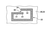
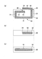
- FIG. 2 is a diagram showing an example of a surface arrangement configuration of the capacitive coupling portion in a plan view of the base material portion 30, and is shown from a viewpoint from the normal direction of the first surface 33 of the base material portion 30.
- the normal direction of the first surface 33 is a direction parallel to the Z axis (see FIG. 1).
- the radiating element 22 and the gap 60 are located on the first surface 33.
- the first tip portion 23 and the second tip portion 24 oppose each other in the element width direction of the second conductor element 51 and the third conductor element 52.
- the gap 60 is formed between the first tip portion 23 and the second tip portion 24 in the element width direction.
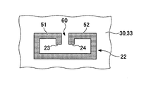
- FIG. 3 is a diagram showing another example of the surface arrangement configuration of the capacitive coupling portion in a plan view of the base material portion 30, and is shown from a viewpoint from the normal direction of the first surface 33 of the base material portion 30.
- the radiating element 22 and the gap 60 are located on the first surface 33.
- the first tip portion 23 and the second tip portion 24 oppose each other in the longitudinal direction of the second conductor element 51 and the third conductor element 52.
- the gap 60 is formed between the first tip portion 23 and the second tip portion 24 in the longitudinal direction.
- the first tip portion 23 bends at right angles to the longitudinal direction of the second conductor element 51, and the second tip portion 24 bends at right angles to the longitudinal direction of the third conductor element 52.
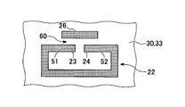
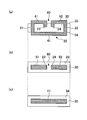
- FIG. 4 is a diagram showing another example of the surface arrangement configuration of the capacitive coupling portion in a plan view of the base material portion 30, and is shown from a viewpoint from the normal direction of the first surface 33 of the base material portion 30.
- the radiating element 22 and the gap 60 are located on the first surface 33.
- the antenna 25 includes a fourth conductor element 26 located on the first surface 33.
- the fourth conductor element 26 is an example of a third conductor portion.
- the fourth conductor element 26 is capacitively coupled to the second conductor element 51 and the third conductor element 52 via the gap 60.
- the first tip portion 23 and the second tip portion 24 face each other in the longitudinal direction of the second conductor element 51 and the third conductor element 52, and are capacitively coupled via the first gap 60. To do.
- the first gap 60 is formed between the first tip portion 23 and the second tip portion 24 in the longitudinal direction.
- the first tip portion 23 of the second conductor element 51 and one tip portion of the fourth conductor element 26 are opposed to each other in the element width direction of the second conductor element 51 and the fourth conductor element 26. , Capacitively coupled through the second gap 60.
- the second gap 60 is formed between the first tip portion 23 and the one tip portion in the element width direction.
- the second tip 24 of the third conductor element 52 and the other tip of the fourth conductor element 26 face each other in the element width direction of the third conductor element 52 and the fourth conductor element 26. And capacitively coupled through the third gap 60.
- the third gap 60 is formed between the second tip 24 and the other tip in the element width direction.
- the first tip portion 23 and the second tip portion 24 are in contact with the first surface 33 of the base material portion 30 having a dielectric loss tangent of 0.01 or less.
- the degree of improvement of the radiation efficiency ⁇ with respect to the length of the gap 60 shortened is increased.
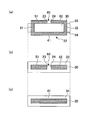
- FIG. 5 to 8 are diagrams showing an example of a stacked arrangement configuration of the capacitive coupling portion.
- a of each figure is a figure which shows an example of the cross section parallel to the lamination direction.
- B) of each figure is a figure which shows an example of a structure by the side of the 1st surface 33 of the base material part 30.
- C) of each figure is a figure which shows an example of the structure by the side of the 2nd surface 34 of the base material part 30.
- the second surface 34 is the surface opposite to the first surface 33.
- the second conductor element 51, the third conductor element 52, and the gap 60 are located on the first surface 33.
- the first conductor element 41 is located on the second surface 34.
- the first tip portion 23 and the second tip portion 24 oppose each other in the longitudinal direction of the second conductor element 51 and the third conductor element 52.
- the gap 60 is formed between the first tip portion 23 and the second tip portion 24 in the longitudinal direction.
- the first conductor element 41 has one end connected to the first outer end portion of the second conductor element 51 via the first via 31 and the second outer end portion of the third conductor element 52. And the other end connected via the second via 32.
- the first via 31 and the second via 32 penetrate the base material portion 30.
- the first tip portion 23 and the second tip portion 24 are in contact with the first surface 33 of the base material portion 30 having a dielectric loss tangent of 0.01 or less.
- the degree of improvement of the radiation efficiency ⁇ with respect to the length obtained by shortening the gap length is increased.
- the third conductor element 52 is located on the first surface 33.
- the second conductor element 51 and the gap 60 are located inside the base material portion 30.
- the first conductor element 41 is located on the second surface 34.
- the first tip portion 23 and the second tip portion 24 oppose each other in the element width direction of the second conductor element 51 and the third conductor element 52.
- the gap 60 is formed between the first tip portion 23 and the second tip portion 24 in the element width direction.
- the first tip 23 is bent at a right angle with respect to the longitudinal direction of the second conductor element 51, and the second tip 24 is at a right angle with respect to the longitudinal direction of the third conductor element 52. Bend.
- the gap 60 has a portion located on the first surface 33 of the base material portion 30 and a portion located inside the base material portion 30.
- the fourth conductor element 26 is capacitively coupled to the second conductor element 51 and the third conductor element 52 via the gap 60. As in the case of FIG. 4, three gaps 60 are formed. Each gap 60 is located inside the base material portion 30.
- the radiation efficiency ⁇ is improved with respect to the length of the gap 60 shortened.
- the degree increases.
- FIG. 9 is a diagram showing an example of the configuration of the antenna 25 during simulation in plan view.
- FIG. 10 is a diagram illustrating an example of a laminated configuration during simulation of the antenna 25.
- the feeding element 21 and the ground 14 are disposed on the feeding element layer 16, and the radiating element 22 and the base material portion 30 are disposed on the radiating element layer 15.
- FIG. 11 is a diagram illustrating an example of a configuration of the radiating element 22 and the power feeding element 21 during simulation.
- the gap on the horizontal axis represents the gap length of the gap 60 between the first tip portion 23 and the second tip portion 24.
- the resonance frequency on the vertical axis represents the resonance frequency of the antenna 25. As shown in FIG. 12, even if the dielectric loss tangent is changed from 0.0001 to 0.1, the resonance frequency hardly changes if the gap length is the same.
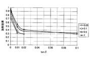
- FIG. 13 is a diagram illustrating an example of the relationship between the dielectric loss tangent and the radiation efficiency ⁇ due to the difference in gap length of the gap 60.
- FIG. 13 shows four cases in which the gap length gap is 0.05 mm, 0.1 mm, 0.5 mm, and 1 mm.
- a portion that is not plotted indicates a region where the antenna 25 does not function as an antenna.
- FIG. 14 is a cross-sectional view schematically showing an example of the configuration of the antenna 25 mounted on a prototype of an actual electronic device.
- the ground 114 is a specific example of the ground 14, the power feeding element 121 is a specific example of the power feeding element 21, and the radiation element 122 is a specific example of the radiation element 22.
- the substrate 113 is an FR4 substrate that is a specific example of the substrate 13.
- the end 112 is a specific example of the end 12 (feeding point).
- the film 130 is a specific example of the base material portion 30 having a dielectric loss tangent greater than 0 and 0.01 or less.
- the radiating element 122 is attached to the inner surface of the glass plate 118 through the film 130.
- the glass plate 118 is a back cover of the electronic device.
- the substrate 113 is attached to a metal casing 117 of the electronic device by at least one attachment portion 119.
- the ground 114 is grounded to the housing 117 via at least one connection part 120.
- the radiating element 122 is an open loop resonant antenna having a gap 60.
- the conductor strip 126 is a specific example of the fourth conductor element 26 described above. In FIG. 14, the conductor strip 126 is not shown.
- the conductor strip 126 is disposed to face the gap 60 through the film 130 so as to be capacitively coupled to the conductor elements on both sides forming the gap 60. That is, the open-loop resonant antenna (radiating element 122) has a structure that can be capacitively coupled to the conductor strip 126 in a direction perpendicular to the film 130.
- the conductor strip 126 is provided between the inner surface of the glass plate 118 and the film 130, and is in contact with both the inner surface of the glass plate 118 and the film 130.
- the radiating element 122 is located on the opposite side of the glass plate 118 with respect to the film 130 so as to be separated from the glass plate 118. .
- FIG. 16 is a plan view showing the part shown in FIG. 15 from the viewpoint from the conductor strip 126 side with respect to the film 130.
- the illustration of the glass plate 118 is omitted. Both end portions of the conductor strip 126 are opposed to the conductor elements on both sides forming the gap 60 through the film 130.
- FIG. 17 is a diagram showing the antenna 25 shown in FIG. 14 in plan view.
- FIG. 18 is a diagram showing the radiating element 122 and the conductor strip 126 of the antenna 25 shown in FIG. 17 in plan view.
- FIG. 19 is a diagram showing the feeding element 121 of the antenna 25 shown in FIG. 17 in plan view.
- FIG. 20 is a diagram showing the relative dielectric constant and dielectric loss tangent (tan ⁇ ) of each material.
- FIG. 21 is a diagram illustrating an example of a result of actual measurement of total efficiency due to a difference in material of the film 130.
- FIG. 22 is a diagram illustrating an example of a result of actual measurement of the reflection coefficient S11 due to a difference in material of the film 130.
- the total efficiency represents the product of the radiation efficiency ⁇ and the reflection coefficient S11. That is, the total efficiency represents the radiation efficiency with the return loss of the antenna 25 taken into account.
- FIG. 23 is a diagram illustrating an example of a result of calculation on the simulation of the relationship between the distance between the feeding element 21 and the radiating element 22 and the radiation efficiency in the configuration of the antenna 25 illustrated in FIGS. 9 to 11.
- FIG. 23 shows a case where tan ⁇ is 0.01.
- the horizontal axis represents the shortest distance D between the feeding element 21 and the radiating element 22.
- the vertical axis represents the radiation efficiency ⁇ .
- gap represents the gap length of the gap 60 between the first tip portion 23 and the second tip portion 24.
- ⁇ represents the wavelength of the radio wave transmitted or received by the antenna 25.
- the radiation efficiency ⁇ is 50% or more when the gap length is 1 mm.
- the radiation efficiency ⁇ is less than 50%, but by changing tan ⁇ to a value smaller than 0.01, the radiation efficiency ⁇ should be 50% or more. Can do.
- the antenna has been described in the embodiment, but the present invention is not limited to the above embodiment.
- Various modifications and improvements such as combinations and substitutions with some or all of the other embodiments are possible within the scope of the present invention.
Abstract
Provided is an antenna that is equipped with a ground plane, a first resonator connected to a power feeding point having the ground plane as a reference, and a second resonator to which power is fed by the first resonator via electromagnetic field coupling in a non-contacting state. The second resonator includes a first conductor part and a second conductor part capacitively coupled to the first conductor part via a gap. The dielectric loss tangent of the base part on which the second resonator is formed is greater than 0 but does not exceed 0.01.
Description
本発明は、アンテナに関する。
The present invention relates to an antenna.
従来、グランドプレーンと、前記グランドプレーンを基準とする給電点に接続された第1の共振器と、前記第1の共振器によって電磁界結合で非接触に給電される第2の共振器とを備える、アンテナが知られている。
Conventionally, a ground plane, a first resonator connected to a feeding point with the ground plane as a reference, and a second resonator fed in a non-contact manner by electromagnetic coupling by the first resonator An antenna is known.
第2の共振器が、第1の導体部と、第1の導体部にギャップを介して容量結合する第2の導体部とを有する形態では、共振周波数を固定した場合、当該ギャップを狭めることで当該ギャップを挟む容量結合部の容量は増えるので、アンテナの小型化が可能である。しかしながら、当該ギャップを狭めるほど、アンテナの放射効率が低下する場合がある。
In the form in which the second resonator has the first conductor portion and the second conductor portion that is capacitively coupled to the first conductor portion via the gap, when the resonance frequency is fixed, the gap is narrowed. Thus, the capacity of the capacitive coupling portion sandwiching the gap increases, so that the antenna can be downsized. However, as the gap is narrowed, the radiation efficiency of the antenna may decrease.
そこで、本発明の一態様は、小型化と放射効率の向上との両立が可能なアンテナを提供することを目的とする。
Therefore, an object of one embodiment of the present invention is to provide an antenna that can achieve both reduction in size and improvement in radiation efficiency.
上記目的を達成するため、本発明の一態様によれば、
グランドプレーンと、
前記グランドプレーンを基準とする給電点に接続された第1の共振器と、
前記第1の共振器によって電磁界結合で非接触に給電される第2の共振器とを備え、
前記第2の共振器は、第1の導体部と、前記第1の導体部にギャップを介して容量結合する第2の導体部とを有し、
前記第2の共振器が形成された基材部の誘電正接は、0よりも大きく0.01以下である、アンテナが提供される。 In order to achieve the above object, according to one aspect of the present invention,
A ground plane,
A first resonator connected to a feed point with respect to the ground plane;
A second resonator that is fed in a non-contact manner by electromagnetic coupling by the first resonator;
The second resonator includes a first conductor portion and a second conductor portion that is capacitively coupled to the first conductor portion via a gap.
An antenna is provided in which the dielectric loss tangent of the base material portion on which the second resonator is formed is greater than 0 and less than or equal to 0.01.
本案によれば、前記第2の共振器が形成された基材部の誘電正接は、0よりも大きく0.01以下であるので、当該ギャップを狭めても、放射効率を向上させることができる。したがって、アンテナの小型化と放射効率の向上とを両立させることができる。
According to the present plan, since the dielectric loss tangent of the base material portion on which the second resonator is formed is greater than 0 and 0.01 or less, the radiation efficiency can be improved even if the gap is narrowed. . Therefore, both miniaturization of the antenna and improvement of the radiation efficiency can be achieved.
以下、本発明の実施形態を図面を参照して説明する。
Hereinafter, embodiments of the present invention will be described with reference to the drawings.
図1は、一実施形態に係るアンテナ25のシミュレーションモデルの構成の一例を示す斜視図である。アンテナ25は、電子機器に搭載される。電子機器は、アンテナ25を用いて無線通信を行う。
FIG. 1 is a perspective view showing an example of the configuration of a simulation model of the antenna 25 according to an embodiment. The antenna 25 is mounted on an electronic device. The electronic device performs wireless communication using the antenna 25.
アンテナ25が搭載される電子機器とは、例えば、無線通信モジュール、据え置き型のテレビやパソコン等の表示機器自体、表示機器に搭載される装置、移動体自体、又は移動体に搭載される装置である。移動体の具体例として、携帯可能な携帯端末装置、自動車等の車両、ロボットなどが挙げられる。携帯端末装置の具体例として、携帯電話、スマートフォン、コンピュータ、ゲーム機、テレビ、音楽や映像のプレーヤー、ウェアラブルデバイスなどが挙げられる。ウェアラブルデバイスの具体的な形態として、リストウォッチ型、ペンダント型、メガネ型などが挙げられる。
The electronic device on which the antenna 25 is mounted is, for example, a wireless communication module, a display device itself such as a stationary television or a personal computer, a device mounted on the display device, a mobile body itself, or a device mounted on the mobile body. is there. Specific examples of the mobile object include a portable terminal device, a vehicle such as an automobile, and a robot. Specific examples of the mobile terminal device include a mobile phone, a smartphone, a computer, a game machine, a television, a music and video player, and a wearable device. Specific examples of the wearable device include a wristwatch type, a pendant type, and a glasses type.
アンテナ25は、例えば、ブルートゥース(登録商標)等の無線通信規格、IEEE802.11ac等の無線LAN(Local Area Network)規格に対応する。アンテナ25は、グランド14を利用する伝送線路の終端12に接続される。
The antenna 25 corresponds to, for example, a wireless communication standard such as Bluetooth (registered trademark) or a wireless LAN (Local Area Network) standard such as IEEE802.11ac. The antenna 25 is connected to the end 12 of the transmission line using the ground 14.
伝送線路の具体例として、マイクロストリップライン、ストリップライン、グランドプレーン付きコプレーナウェーブガイド(信号線の形成される導体面とは反対側の表面にグランドプレーンが配置されたコプレーナウェーブガイド)、コプレーナストリップラインなどが挙げられる。
Specific examples of transmission lines include microstrip lines, strip lines, coplanar waveguides with ground planes (coplanar waveguides having a ground plane disposed on the surface opposite to the conductor surface on which signal lines are formed), and coplanar strip lines. Etc.
アンテナ25は、グランド14と、給電素子21と、放射素子22とを備える。
The antenna 25 includes a ground 14, a feeding element 21, and a radiating element 22.
グランド14は、グランドプレーンの一例である。グランド外縁14aは、グランド14の直線的な外縁の一例である。グランド14は、例えば、XY平面に平行な基板13に形成されたグランドパターンである。
The ground 14 is an example of a ground plane. The ground outer edge 14 a is an example of a linear outer edge of the ground 14. The ground 14 is a ground pattern formed on the substrate 13 parallel to the XY plane, for example.
基板13は、誘電体を主成分とする部材である。基板13の具体例として、FR4(Flame Retardant Type4)基板が挙げられる。基板13は、可撓性を有するフレキシブル基板でもよい。基板13は、第1の基板表面と、第1の基板表面とは反対側の第2の基板表面とを有する。例えば、第1の基板表面には、電子回路が実装され、第2の基板表面には、グランド14が形成されている。なお、グランド14は、第1の基板表面に形成されていても、基板13の内部に形成されていてもよい。
The substrate 13 is a member whose main component is a dielectric. A specific example of the substrate 13 is an FR4 (Flame Retardant Type 4) substrate. The substrate 13 may be a flexible substrate having flexibility. The substrate 13 has a first substrate surface and a second substrate surface opposite to the first substrate surface. For example, an electronic circuit is mounted on the first substrate surface, and a ground 14 is formed on the second substrate surface. The ground 14 may be formed on the surface of the first substrate or may be formed inside the substrate 13.
基板13に実装される電子回路は、例えば、アンテナ25を介して信号を受信する受信機能と、アンテナ25を介して信号を送信する送信機能との少なくとも一方の機能を含む集積回路である。電子回路は、例えば、ICチップによって実現される。
The electronic circuit mounted on the substrate 13 is, for example, an integrated circuit including at least one of a reception function for receiving a signal via the antenna 25 and a transmission function for transmitting a signal via the antenna 25. The electronic circuit is realized by, for example, an IC chip.
給電素子21は、グランドプレーンを基準とする給電点に接続された第1の共振器の一例である。給電素子21は、伝送線路の終端12に接続されている。終端12は、グランド14をグランド基準とする給電点の一例である。
The feeding element 21 is an example of a first resonator connected to a feeding point with a ground plane as a reference. The feed element 21 is connected to the end 12 of the transmission line. The terminal end 12 is an example of a feeding point with the ground 14 as a ground reference.
給電素子21は、基板13に配置されてもよいし、基板13以外の箇所に配置されてもよい。給電素子21が基板13に配置されている場合、給電素子21は、例えば、基板13の第1の基板表面に形成された導体パターンである。
The power feeding element 21 may be disposed on the substrate 13 or may be disposed at a place other than the substrate 13. When the power feeding element 21 is disposed on the substrate 13, the power feeding element 21 is, for example, a conductor pattern formed on the first substrate surface of the substrate 13.
給電素子21は、グランド14から離れる方向に延伸し、グランド14をグランド基準とする給電点(終端12)に接続されている。給電素子21は、放射素子22に対して非接触で高周波的に結合して給電可能な線状導体である。図面には、グランド外縁14aに対して直角な方向に延在する直線状導体と、グランド外縁14aに並走して延在する直線状導体とによって、L字状に形成された給電素子21が例示されている。図示の場合、給電素子21は、終端12を起点に端部21aから延伸してから曲折部21cで折れ曲がり、先端部21bまで延伸する。先端部21bは、他の導体が接続されていない開放端である。図面には、L字状の給電素子21が例示されているが、給電素子21の形状は、直線状、メアンダ状、ループ状などの他の形状でもよい。
The feeding element 21 extends in a direction away from the ground 14, and is connected to a feeding point (termination 12) with the ground 14 as a ground reference. The feeding element 21 is a linear conductor that can be fed to the radiating element 22 in a non-contact manner in a high frequency manner. In the drawing, a feeding element 21 formed in an L shape by a linear conductor extending in a direction perpendicular to the ground outer edge 14a and a linear conductor extending parallel to the ground outer edge 14a is shown. Illustrated. In the illustrated case, the power feeding element 21 extends from the end portion 21a with the terminal end 12 as a starting point, then bends at the bent portion 21c, and extends to the front end portion 21b. The tip portion 21b is an open end to which no other conductor is connected. Although the L-shaped feeding element 21 is illustrated in the drawing, the shape of the feeding element 21 may be other shapes such as a straight line shape, a meander shape, and a loop shape.
放射素子22は、第1の共振器に近接する第2の共振器の一例である。放射素子22は、例えば、給電素子21から離れて配置され、給電素子21が共振することにより放射導体として機能する。放射素子22は、例えば、給電素子21と電磁界結合することにより非接触に給電されて放射導体として機能する。電磁界結合とは、電磁波による非接触結合を意味する。
The radiating element 22 is an example of a second resonator close to the first resonator. For example, the radiating element 22 is disposed away from the power feeding element 21 and functions as a radiating conductor when the power feeding element 21 resonates. For example, the radiating element 22 functions as a radiating conductor by being fed in a non-contact manner by electromagnetic coupling with the feeding element 21. Electromagnetic field coupling means non-contact coupling by electromagnetic waves.
放射素子22は、グランド外縁14aに沿うように延伸する導体部分を有する。図面には、導体部分として、導体エレメント41,51,52が示されている。導体部分は、グランド外縁14aから離れて位置する。放射素子22がグランド外縁14aに沿った導体部分を有することによって、例えば、アンテナ25の指向性を容易に調整することが可能となる。
The radiating element 22 has a conductor portion extending along the ground outer edge 14a. In the drawing, conductor elements 41, 51, and 52 are shown as conductor portions. The conductor portion is located away from the ground outer edge 14a. When the radiating element 22 has the conductor portion along the ground outer edge 14a, for example, the directivity of the antenna 25 can be easily adjusted.
給電素子21と放射素子22は、例えば、互いに電磁界結合可能な距離で離れて配置されている。放射素子22は、給電素子21から給電を受ける給電部を有している。図面には、給電部として、第1の導体エレメント41が示されている。放射素子22は、給電部で給電素子21を介して電磁界結合によって非接触で給電される。このように給電されることによって、放射素子22は、アンテナ25の放射導体として機能する。
The feeding element 21 and the radiating element 22 are arranged, for example, separated by a distance that allows electromagnetic coupling to each other. The radiating element 22 includes a power feeding unit that receives power from the power feeding element 21. In the drawing, a first conductor element 41 is shown as a power feeding unit. The radiating element 22 is fed in a non-contact manner by electromagnetic coupling through the feeding element 21 in the feeding section. By being fed in this way, the radiating element 22 functions as a radiating conductor of the antenna 25.
放射素子22は、給電素子21によって電磁界結合で非接触に給電されることにより、半波長ダイポールアンテナと同様の共振電流(一方の先端部23と他方の先端部24との間を定在波状に分布する電流)が放射素子22上に流れる。すなわち、放射素子22は、給電素子21によって電磁界結合で非接触に給電されることにより、ダイポールアンテナとして機能する。
The radiating element 22 is fed in a non-contact manner by electromagnetic coupling by the feeding element 21, so that a resonance current similar to that of the half-wavelength dipole antenna (a standing wave shape between one tip portion 23 and the other tip portion 24). Current distributed on the radiation element 22. That is, the radiating element 22 functions as a dipole antenna by being fed in a non-contact manner by electromagnetic coupling by the feeding element 21.
放射素子22は、第1の導体エレメント41と、第2の導体エレメント51と、第3の導体エレメント52とを有する。第2の導体エレメント51は、第1の導体部の一例である。第3の導体エレメント52は、第2の導体部の一例である。
The radiating element 22 includes a first conductor element 41, a second conductor element 51, and a third conductor element 52. The second conductor element 51 is an example of a first conductor portion. The third conductor element 52 is an example of a second conductor portion.
第1の導体エレメント41は、第2の導体エレメント51に接続される一端と、第3の導体エレメント52に接続される他端とを有する。第2の導体エレメント51は、第1の導体エレメント41に対して当該一端で折り返されて延在し、第3の導体エレメント52は、第1の導体エレメント41に対して当該他端で折り返されて延在する。
The first conductor element 41 has one end connected to the second conductor element 51 and the other end connected to the third conductor element 52. The second conductor element 51 is folded and extended at the one end with respect to the first conductor element 41, and the third conductor element 52 is folded at the other end with respect to the first conductor element 41. Extend.
第2の導体エレメント51の第1の先端部23と、第3の導体エレメント52の第2の先端部24とは、ギャップ60を介して離れている。つまり、放射素子22の形状は、ギャップ60で開放する開ループであり、放射素子22は、ギャップ60を有する開ループ共振アンテナである。第2の導体エレメント51が有する第1の先端部23は、放射素子22の一方の先端部であり、第3の導体エレメント52が有する第2の先端部24は、放射素子22の他方の先端部である。
The first tip portion 23 of the second conductor element 51 and the second tip portion 24 of the third conductor element 52 are separated from each other via a gap 60. That is, the shape of the radiating element 22 is an open loop that opens at the gap 60, and the radiating element 22 is an open loop resonant antenna having the gap 60. The first tip 23 of the second conductor element 51 is one tip of the radiating element 22, and the second tip 24 of the third conductor element 52 is the other tip of the radiating element 22. Part.
本実施形態では、第2の導体エレメント51と第3の導体エレメント52とは、ギャップ60を介して容量的に結合する。図1の場合、第1の先端部23と第2の先端部24とがギャップ60を介して容量的に結合する。つまり、放射素子22は、第1の先端部23と第2の先端部24とでギャップ60を挟んだ容量結合部を有する。
In the present embodiment, the second conductor element 51 and the third conductor element 52 are capacitively coupled through the gap 60. In the case of FIG. 1, the first tip portion 23 and the second tip portion 24 are capacitively coupled through the gap 60. That is, the radiating element 22 has a capacitive coupling portion in which the gap 60 is sandwiched between the first tip portion 23 and the second tip portion 24.
第1の先端部23と第2の先端部24とは、第2の導体エレメント51と第3の導体エレメント52のそれぞれの長手方向で対向する。ギャップ60は、当該長手方向で第1の先端部23と第2の先端部24との間に形成されている。
The first tip portion 23 and the second tip portion 24 oppose each other in the longitudinal direction of the second conductor element 51 and the third conductor element 52. The gap 60 is formed between the first tip portion 23 and the second tip portion 24 in the longitudinal direction.
放射素子22は、誘電性の基材部30に設けられている。基材部30は、例えば、平面部を有する基板である。放射素子22の一部又は全部は、基材部30の表面に設けられてもよいし、基材部30の内部に設けられてもよい。
The radiating element 22 is provided on the dielectric base 30. The base material part 30 is a board | substrate which has a plane part, for example. Part or all of the radiating element 22 may be provided on the surface of the base member 30 or may be provided inside the base member 30.
放射素子22の共振周波数を固定した場合、ギャップ60のギャップ長が短いほど、第2の導体エレメント51と第3の導体エレメント52とでギャップ60を挟んだ容量結合部の容量は増えるので、放射素子22の小型化が可能である。放射素子22の小型化によりアンテナ25の小型化が可能である。ギャップ60は、直線で形成されているが、櫛状のインターディジタル構造で形成されてもよい。
When the resonance frequency of the radiating element 22 is fixed, the shorter the gap length of the gap 60, the larger the capacitance of the capacitive coupling portion sandwiching the gap 60 between the second conductor element 51 and the third conductor element 52. The element 22 can be downsized. The antenna 25 can be downsized by reducing the size of the radiating element 22. The gap 60 is formed in a straight line, but may be formed in a comb-like interdigital structure.
しかしながら、放射素子22の容量結合部のギャップ長が短くなると、アンテナ25の放射効率ηが劣化する。放射効率ηは、アンテナ25への供給電力に対する放射電力の比率を表す。放射効率ηの劣化は、放射素子22が形成された基材部30の誘電正接(tanδ)に起因する。
However, when the gap length of the capacitive coupling portion of the radiating element 22 is shortened, the radiation efficiency η of the antenna 25 is deteriorated. The radiation efficiency η represents the ratio of the radiated power to the power supplied to the antenna 25. The deterioration of the radiation efficiency η is caused by the dielectric loss tangent (tan δ) of the base material portion 30 on which the radiation element 22 is formed.
そこで、本実施形態では、基材部30の誘電正接(tanδ)は、0よりも大きく0.01以下に設定されている。これにより、放射素子22の共振周波数を固定した場合、ギャップ60を狭くしても、tanδが0.01よりも大きな場合と比較して放射効率ηを向上させることができる。したがって、アンテナ25の小型化と放射効率ηの向上が両立する。
Therefore, in this embodiment, the dielectric loss tangent (tan δ) of the base material portion 30 is set to be larger than 0 and 0.01 or less. Thereby, when the resonance frequency of the radiation element 22 is fixed, even if the gap 60 is narrowed, the radiation efficiency η can be improved as compared with the case where tan δ is larger than 0.01. Therefore, the miniaturization of the antenna 25 and the improvement of the radiation efficiency η are compatible.
また、アンテナ25が送信又は受信する電波の波長をλとしたとき、給電素子21と放射素子22との最短距離は、0よりも大きく0.117×λ以下であることが、アンテナ25の小型化と放射効率ηの向上とを両立させる点で好ましい。より好ましくは、0.07×λ以下であり、さらに好ましくは、0.04×λ以下である。
Further, when the wavelength of a radio wave transmitted or received by the antenna 25 is λ, the shortest distance between the feeding element 21 and the radiating element 22 is greater than 0 and 0.117 × λ or less. Is preferable in terms of achieving both improvement of the efficiency and radiation efficiency η. More preferably, it is 0.07 × λ or less, and further preferably 0.04 × λ or less.
図2は、容量結合部の面配置構成の一例を基材部30の平面視で示す図であり、基材部30の第1の表面33の法線方向からの視点で示す。第1の表面33の法線方向は、Z軸(図1参照)に平行な方向である。放射素子22及びギャップ60は、第1の表面33上に位置する。第1の先端部23と第2の先端部24とは、第2の導体エレメント51と第3の導体エレメント52のそれぞれのエレメント幅方向で対向する。ギャップ60は、当該エレメント幅方向で第1の先端部23と第2の先端部24との間に形成されている。
FIG. 2 is a diagram showing an example of a surface arrangement configuration of the capacitive coupling portion in a plan view of the base material portion 30, and is shown from a viewpoint from the normal direction of the first surface 33 of the base material portion 30. The normal direction of the first surface 33 is a direction parallel to the Z axis (see FIG. 1). The radiating element 22 and the gap 60 are located on the first surface 33. The first tip portion 23 and the second tip portion 24 oppose each other in the element width direction of the second conductor element 51 and the third conductor element 52. The gap 60 is formed between the first tip portion 23 and the second tip portion 24 in the element width direction.
図3は、容量結合部の面配置構成の他の一例を基材部30の平面視で示す図であり、基材部30の第1の表面33の法線方向からの視点で示す。放射素子22及びギャップ60は、第1の表面33上に位置する。第1の先端部23と第2の先端部24とは、第2の導体エレメント51と第3の導体エレメント52のそれぞれの長手方向で対向する。ギャップ60は、当該長手方向で第1の先端部23と第2の先端部24との間に形成されている。第1の先端部23は、第2の導体エレメント51の長手方向に対して直角に曲がり、第2の先端部24は、第3の導体エレメント52の長手方向に対して直角に曲がる。
FIG. 3 is a diagram showing another example of the surface arrangement configuration of the capacitive coupling portion in a plan view of the base material portion 30, and is shown from a viewpoint from the normal direction of the first surface 33 of the base material portion 30. The radiating element 22 and the gap 60 are located on the first surface 33. The first tip portion 23 and the second tip portion 24 oppose each other in the longitudinal direction of the second conductor element 51 and the third conductor element 52. The gap 60 is formed between the first tip portion 23 and the second tip portion 24 in the longitudinal direction. The first tip portion 23 bends at right angles to the longitudinal direction of the second conductor element 51, and the second tip portion 24 bends at right angles to the longitudinal direction of the third conductor element 52.
図4は、容量結合部の面配置構成の他の一例を基材部30の平面視で示す図であり、基材部30の第1の表面33の法線方向からの視点で示す。放射素子22及びギャップ60は、第1の表面33上に位置する。アンテナ25は、第1の表面33上に位置する第4の導体エレメント26を備える。第4の導体エレメント26は、第3の導体部の一例である。第4の導体エレメント26は、第2の導体エレメント51及び第3の導体エレメント52にギャップ60を介して容量結合する。
FIG. 4 is a diagram showing another example of the surface arrangement configuration of the capacitive coupling portion in a plan view of the base material portion 30, and is shown from a viewpoint from the normal direction of the first surface 33 of the base material portion 30. The radiating element 22 and the gap 60 are located on the first surface 33. The antenna 25 includes a fourth conductor element 26 located on the first surface 33. The fourth conductor element 26 is an example of a third conductor portion. The fourth conductor element 26 is capacitively coupled to the second conductor element 51 and the third conductor element 52 via the gap 60.
第1の先端部23と第2の先端部24とは、第2の導体エレメント51と第3の導体エレメント52のそれぞれの長手方向で対向し、第1のギャップ60を介して容量的に結合する。第1のギャップ60は、当該長手方向で第1の先端部23と第2の先端部24との間に形成されている。
The first tip portion 23 and the second tip portion 24 face each other in the longitudinal direction of the second conductor element 51 and the third conductor element 52, and are capacitively coupled via the first gap 60. To do. The first gap 60 is formed between the first tip portion 23 and the second tip portion 24 in the longitudinal direction.
第2の導体エレメント51の第1の先端部23と第4の導体エレメント26の一方の先端部とは、第2の導体エレメント51と第4の導体エレメント26のそれぞれのエレメント幅方向で対向し、第2のギャップ60を介して容量的に結合する。第2のギャップ60は、当該エレメント幅方向で第1の先端部23と当該一方の先端部との間に形成されている。
The first tip portion 23 of the second conductor element 51 and one tip portion of the fourth conductor element 26 are opposed to each other in the element width direction of the second conductor element 51 and the fourth conductor element 26. , Capacitively coupled through the second gap 60. The second gap 60 is formed between the first tip portion 23 and the one tip portion in the element width direction.
第3の導体エレメント52の第2の先端部24と第4の導体エレメント26の他方の先端部とは、第3の導体エレメント52と第4の導体エレメント26のそれぞれのエレメント幅方向で対向し、第3のギャップ60を介して容量的に結合する。第3のギャップ60は、当該エレメント幅方向で第2の先端部24と当該他方の先端部との間に形成されている。
The second tip 24 of the third conductor element 52 and the other tip of the fourth conductor element 26 face each other in the element width direction of the third conductor element 52 and the fourth conductor element 26. And capacitively coupled through the third gap 60. The third gap 60 is formed between the second tip 24 and the other tip in the element width direction.
図2~図4の構成によれば、第1の先端部23及び第2の先端部24が、0.01以下の誘電正接を有する基材部30の第1の表面33に接しているので、ギャップ60のギャップ長を短縮した長さに対する放射効率ηの向上度合いが増す。
2 to 4, the first tip portion 23 and the second tip portion 24 are in contact with the first surface 33 of the base material portion 30 having a dielectric loss tangent of 0.01 or less. The degree of improvement of the radiation efficiency η with respect to the length of the gap 60 shortened is increased.
図5~8は、容量結合部の積層配置構成の一例を示す図である。各図の(a)は、積層方向に平行な断面の一例を示す図である。各図の(b)は、基材部30の第1の表面33側の構成の一例を示す図である。各図の(c)は、基材部30の第2の表面34側の構成の一例を示す図である。第2の表面34は、第1の表面33とは反対側の表面である。
5 to 8 are diagrams showing an example of a stacked arrangement configuration of the capacitive coupling portion. (A) of each figure is a figure which shows an example of the cross section parallel to the lamination direction. (B) of each figure is a figure which shows an example of a structure by the side of the 1st surface 33 of the base material part 30. As shown in FIG. (C) of each figure is a figure which shows an example of the structure by the side of the 2nd surface 34 of the base material part 30. As shown in FIG. The second surface 34 is the surface opposite to the first surface 33.
図5において、第2の導体エレメント51、第3の導体エレメント52及びギャップ60は、第1の表面33上に位置する。第1の導体エレメント41は、第2の表面34上に位置する。第1の先端部23と第2の先端部24とは、第2の導体エレメント51と第3の導体エレメント52のそれぞれの長手方向で対向する。ギャップ60は、当該長手方向で第1の先端部23と第2の先端部24との間に形成されている。
In FIG. 5, the second conductor element 51, the third conductor element 52, and the gap 60 are located on the first surface 33. The first conductor element 41 is located on the second surface 34. The first tip portion 23 and the second tip portion 24 oppose each other in the longitudinal direction of the second conductor element 51 and the third conductor element 52. The gap 60 is formed between the first tip portion 23 and the second tip portion 24 in the longitudinal direction.
第1の導体エレメント41は、第2の導体エレメント51の第1の外側端部に第1のビア31を介して接続された一端と、第3の導体エレメント52の第2の外側端部に第2のビア32を介して接続された他端とを有する。第1のビア31及び第2のビア32は、基材部30を貫通する。
The first conductor element 41 has one end connected to the first outer end portion of the second conductor element 51 via the first via 31 and the second outer end portion of the third conductor element 52. And the other end connected via the second via 32. The first via 31 and the second via 32 penetrate the base material portion 30.
図5の構成によれば、第1の先端部23及び第2の先端部24が、0.01以下の誘電正接を有する基材部30の第1の表面33に接しているので、ギャップ60のギャップ長を短縮した長さに対する放射効率ηの向上度合いが増す。
According to the configuration of FIG. 5, the first tip portion 23 and the second tip portion 24 are in contact with the first surface 33 of the base material portion 30 having a dielectric loss tangent of 0.01 or less. The degree of improvement of the radiation efficiency η with respect to the length obtained by shortening the gap length is increased.
図6において、第3の導体エレメント52は、第1の表面33上に位置する。第2の導体エレメント51及びギャップ60は、基材部30の内部に位置する。第1の導体エレメント41は、第2の表面34上に位置する。第1の先端部23と第2の先端部24とは、第2の導体エレメント51と第3の導体エレメント52のそれぞれのエレメント幅方向で対向する。ギャップ60は、当該エレメント幅方向で第1の先端部23と第2の先端部24との間に形成されている。
6, the third conductor element 52 is located on the first surface 33. The second conductor element 51 and the gap 60 are located inside the base material portion 30. The first conductor element 41 is located on the second surface 34. The first tip portion 23 and the second tip portion 24 oppose each other in the element width direction of the second conductor element 51 and the third conductor element 52. The gap 60 is formed between the first tip portion 23 and the second tip portion 24 in the element width direction.
図7において、第1の先端部23は、第2の導体エレメント51の長手方向に対して直角に曲がり、第2の先端部24は、第3の導体エレメント52の長手方向に対して直角に曲がる。ギャップ60は、基材部30の第1の表面33上に位置する部分と、基材部30の内部に位置する部分とを有する。
In FIG. 7, the first tip 23 is bent at a right angle with respect to the longitudinal direction of the second conductor element 51, and the second tip 24 is at a right angle with respect to the longitudinal direction of the third conductor element 52. Bend. The gap 60 has a portion located on the first surface 33 of the base material portion 30 and a portion located inside the base material portion 30.
図8において、第4の導体エレメント26は、第2の導体エレメント51及び第3の導体エレメント52にギャップ60を介して容量結合する。図4の場合と同様に、3箇所のギャップ60が形成されている。各ギャップ60は、基材部30の内部に位置する。
8, the fourth conductor element 26 is capacitively coupled to the second conductor element 51 and the third conductor element 52 via the gap 60. As in the case of FIG. 4, three gaps 60 are formed. Each gap 60 is located inside the base material portion 30.
図6~図8の構成によれば、ギャップ60が基材部30の内部(誘電正接は0.01以下)に位置するので、ギャップ60のギャップ長を短縮した長さに対する放射効率ηの向上度合いが増す。
6 to 8, since the gap 60 is located inside the base material portion 30 (dielectric loss tangent is 0.01 or less), the radiation efficiency η is improved with respect to the length of the gap 60 shortened. The degree increases.
図9は、アンテナ25のシミュレーション時の構成の一例を平面視で示す図である。図10は、アンテナ25のシミュレーション時の積層構成の一例を示す図である。給電素子21及びグランド14は、給電素子層16に配置され、放射素子22及び基材部30は、放射素子層15に配置されている。図11は、放射素子22及び給電素子21のシミュレーション時の構成の一例を示す図である。
FIG. 9 is a diagram showing an example of the configuration of the antenna 25 during simulation in plan view. FIG. 10 is a diagram illustrating an example of a laminated configuration during simulation of the antenna 25. The feeding element 21 and the ground 14 are disposed on the feeding element layer 16, and the radiating element 22 and the base material portion 30 are disposed on the radiating element layer 15. FIG. 11 is a diagram illustrating an example of a configuration of the radiating element 22 and the power feeding element 21 during simulation.
図9~図11において、本シミュレーション時の各部の寸法は、単位をmmとすると、
L11:40
L12:60
L13:20
L14:2
L15:14
L16:15.5
L17:2.5
L18:1.9
L19:1.7
L20:2.9
とする。 9 to 11, the dimensions of each part at the time of this simulation are expressed in units of mm.
L11: 40
L12: 60
L13: 20
L14: 2
L15: 14
L16: 15.5
L17: 2.5
L18: 1.9
L19: 1.7
L20: 2.9
And
L11:40
L12:60
L13:20
L14:2
L15:14
L16:15.5
L17:2.5
L18:1.9
L19:1.7
L20:2.9
とする。 9 to 11, the dimensions of each part at the time of this simulation are expressed in units of mm.
L11: 40
L12: 60
L13: 20
L14: 2
L15: 14
L16: 15.5
L17: 2.5
L18: 1.9
L19: 1.7
L20: 2.9
And
図12は、基材部30の誘電正接(=tanδ)の違いによる、容量結合部のギャップ長と共振周波数との関係の一例を示す図である。横軸のgapは、第1の先端部23と第2の先端部24との間のギャップ60のギャップ長を表す。縦軸の共振周波数は、アンテナ25の共振周波数を表す。図12に示されるように、誘電正接を0.0001から0.1まで変化させても、同一ギャップ長であれば、共振周波数はほとんど変化しない。
FIG. 12 is a diagram showing an example of the relationship between the gap length of the capacitive coupling portion and the resonance frequency due to the difference in the dielectric loss tangent (= tan δ) of the base material portion 30. The gap on the horizontal axis represents the gap length of the gap 60 between the first tip portion 23 and the second tip portion 24. The resonance frequency on the vertical axis represents the resonance frequency of the antenna 25. As shown in FIG. 12, even if the dielectric loss tangent is changed from 0.0001 to 0.1, the resonance frequency hardly changes if the gap length is the same.
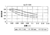
図13は、ギャップ60のギャップ長の違いによる、誘電正接と放射効率ηとの関係の一例を示す図である。図13は、ギャップ長gapが0.05mm,0.1mm,0.5mm,1mmの4つの場合を示す。
FIG. 13 is a diagram illustrating an example of the relationship between the dielectric loss tangent and the radiation efficiency η due to the difference in gap length of the gap 60. FIG. 13 shows four cases in which the gap length gap is 0.05 mm, 0.1 mm, 0.5 mm, and 1 mm.
ギャップ長が0.05mmと0.1mmの場合において、プロットされていない箇所は、アンテナ25がアンテナとして機能しない領域を示す。
When the gap length is 0.05 mm and 0.1 mm, a portion that is not plotted indicates a region where the antenna 25 does not function as an antenna.
図13に示されるように、基材部30の誘電正接(tanδ)は、0よりも大きく0.01以下であると、ギャップ60を狭くしても、tanδが0.01よりも大きな場合と比較して放射効率ηが向上する。したがって、アンテナ25の小型化と放射効率ηの向上が両立している。
As shown in FIG. 13, when the dielectric loss tangent (tan δ) of the base material portion 30 is greater than 0 and less than or equal to 0.01, even when the gap 60 is narrowed, tan δ is greater than 0.01. In comparison, the radiation efficiency η is improved. Therefore, both the miniaturization of the antenna 25 and the improvement of the radiation efficiency η are compatible.
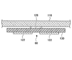
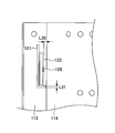
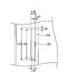
図14は、実際の電子機器の試作品に搭載したアンテナ25の構成の一例を模式的に示す断面図である。グランド114は、グランド14の一具体例であり、給電素子121は、給電素子21の一具体例であり、放射素子122は、放射素子22の一具体例である。基板113は、基板13の一具体例であるFR4基板である。終端112は、終端12(給電点)の一具体例である。フィルム130は、誘電正接が0よりも大きく0.01以下の基材部30の一具体例である。
FIG. 14 is a cross-sectional view schematically showing an example of the configuration of the antenna 25 mounted on a prototype of an actual electronic device. The ground 114 is a specific example of the ground 14, the power feeding element 121 is a specific example of the power feeding element 21, and the radiation element 122 is a specific example of the radiation element 22. The substrate 113 is an FR4 substrate that is a specific example of the substrate 13. The end 112 is a specific example of the end 12 (feeding point). The film 130 is a specific example of the base material portion 30 having a dielectric loss tangent greater than 0 and 0.01 or less.
放射素子122は、フィルム130を介してガラス板118の内側表面に取り付けられている。ガラス板118は、電子機器の裏蓋である。基板113は、電子機器の金属製の筐体117に、少なくとも一つの取り付け部119によって取り付けられている。グランド114は、少なくとも一つの接続部120を介して、筐体117に接地されている。
The radiating element 122 is attached to the inner surface of the glass plate 118 through the film 130. The glass plate 118 is a back cover of the electronic device. The substrate 113 is attached to a metal casing 117 of the electronic device by at least one attachment portion 119. The ground 114 is grounded to the housing 117 via at least one connection part 120.
図15は、図14に示されるアンテナ25において、放射素子122の周辺部を模式的に示す断面図である。放射素子122は、ギャップ60を有する開ループ共振アンテナである。導体ストリップ126は、上述の第4の導体エレメント26の一具体例である。図14では、導体ストリップ126の図示が省略されている。導体ストリップ126は、ギャップ60を形成する両側の導体エレメントに容量結合するように、フィルム130を介してギャップ60に対向して配置されている。すなわち、開ループ共振アンテナ(放射素子122)は、フィルム130に対し垂直方向に導体ストリップ126と容量結合できる構造を有している。このような形態により、開ループのギャップ部分(ギャップ60)がガラス板118に直接的に面していないため、ガラス板118の誘電正接に起因する放射効率の低下を抑制することができる。導体ストリップ126は、ガラス板118の内側表面とフィルム130との間に設けられていて、ガラス板118の内側表面とフィルム130の両方に接触している。
15 is a cross-sectional view schematically showing the periphery of the radiating element 122 in the antenna 25 shown in FIG. The radiating element 122 is an open loop resonant antenna having a gap 60. The conductor strip 126 is a specific example of the fourth conductor element 26 described above. In FIG. 14, the conductor strip 126 is not shown. The conductor strip 126 is disposed to face the gap 60 through the film 130 so as to be capacitively coupled to the conductor elements on both sides forming the gap 60. That is, the open-loop resonant antenna (radiating element 122) has a structure that can be capacitively coupled to the conductor strip 126 in a direction perpendicular to the film 130. With such a configuration, since the open-loop gap portion (gap 60) does not directly face the glass plate 118, a decrease in radiation efficiency due to the dielectric loss tangent of the glass plate 118 can be suppressed. The conductor strip 126 is provided between the inner surface of the glass plate 118 and the film 130, and is in contact with both the inner surface of the glass plate 118 and the film 130.
放射素子122は、フィルム130よりも誘電正接が低いガラス板118の影響を抑えるため、ガラス板118との距離が離れるように、フィルム130に対してガラス板118とは反対側に位置している。
In order to suppress the influence of the glass plate 118 having a dielectric loss tangent lower than that of the film 130, the radiating element 122 is located on the opposite side of the glass plate 118 with respect to the film 130 so as to be separated from the glass plate 118. .
図16は、図15に示される部分を、フィルム130に対して導体ストリップ126側からの視点で示す平面図である。図16では、ガラス板118の図示は省略されている。導体ストリップ126の両端部は、ギャップ60を形成する両側の導体エレメントにフィルム130を介して対向している。
FIG. 16 is a plan view showing the part shown in FIG. 15 from the viewpoint from the conductor strip 126 side with respect to the film 130. In FIG. 16, the illustration of the glass plate 118 is omitted. Both end portions of the conductor strip 126 are opposed to the conductor elements on both sides forming the gap 60 through the film 130.
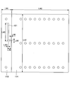
図17は、図14に示されるアンテナ25を平面視で示す図である。図18は、図17に示されるアンテナ25の放射素子122及び導体ストリップ126を平面視で示す図である。図19は、図17に示されるアンテナ25の給電素子121を平面視で示す図である。
FIG. 17 is a diagram showing the antenna 25 shown in FIG. 14 in plan view. FIG. 18 is a diagram showing the radiating element 122 and the conductor strip 126 of the antenna 25 shown in FIG. 17 in plan view. FIG. 19 is a diagram showing the feeding element 121 of the antenna 25 shown in FIG. 17 in plan view.
図20は、各材料の比誘電率及び誘電正接(tanδ)を示す図である。図21は、フィルム130の材料の違いによるトータル効率を実測した結果の一例を示す図である。図22は、フィルム130の材料の違いによる反射係数S11を実測した結果の一例を示す図である。トータル効率は、放射効率ηと反射係数S11との積を表す。つまり、トータル効率は、アンテナ25のリターンロスが加味された放射効率を表す。
FIG. 20 is a diagram showing the relative dielectric constant and dielectric loss tangent (tan δ) of each material. FIG. 21 is a diagram illustrating an example of a result of actual measurement of total efficiency due to a difference in material of the film 130. FIG. 22 is a diagram illustrating an example of a result of actual measurement of the reflection coefficient S11 due to a difference in material of the film 130. In FIG. The total efficiency represents the product of the radiation efficiency η and the reflection coefficient S11. That is, the total efficiency represents the radiation efficiency with the return loss of the antenna 25 taken into account.
図22に示されているように、誘電正接が0.01以下の材料B,Cをフィルム130に使用した場合、所望の共振周波数で良好なインピーダンスマッチングが得られている。また、図21に示されているように、トータル効率については、誘電正接が0.008の材料Bが材料Aよりも優れており、誘電正接が0.001の材料Cが材料Bよりも優れている。
As shown in FIG. 22, when materials B and C having a dielectric loss tangent of 0.01 or less are used for the film 130, good impedance matching is obtained at a desired resonance frequency. Further, as shown in FIG. 21, regarding the total efficiency, the material B having a dielectric loss tangent of 0.008 is superior to the material A, and the material C having a dielectric loss tangent of 0.001 is superior to the material B. ing.
なお、図21,22においてトータル効率及び反射係数を測定した時において、図14~19に示された各部の寸法は、単位をmmとすると、
L24:2.3
L25:3.9
L39:1
L40:1.5
L30:1.3
L31:1.3
L35:1.2
L36:2
L37:0.4
L38:0.4
L33:14.4
L34:13.6
L41:10.5
L42:59.5
L43:18.5
L44:1
L45:1
L46:0.5
L47:60
L48:3.5
である。また、フィルム130の厚さは、50μmである。 When the total efficiency and the reflection coefficient are measured in FIGS. 21 and 22, the dimensions of each part shown in FIGS.
L24: 2.3
L25: 3.9
L39: 1
L40: 1.5
L30: 1.3
L31: 1.3
L35: 1.2
L36: 2
L37: 0.4
L38: 0.4
L33: 14.4
L34: 13.6
L41: 10.5
L42: 59.5
L43: 18.5
L44: 1
L45: 1
L46: 0.5
L47: 60
L48: 3.5
It is. The thickness of thefilm 130 is 50 μm.
L24:2.3
L25:3.9
L39:1
L40:1.5
L30:1.3
L31:1.3
L35:1.2
L36:2
L37:0.4
L38:0.4
L33:14.4
L34:13.6
L41:10.5
L42:59.5
L43:18.5
L44:1
L45:1
L46:0.5
L47:60
L48:3.5
である。また、フィルム130の厚さは、50μmである。 When the total efficiency and the reflection coefficient are measured in FIGS. 21 and 22, the dimensions of each part shown in FIGS.
L24: 2.3
L25: 3.9
L39: 1
L40: 1.5
L30: 1.3
L31: 1.3
L35: 1.2
L36: 2
L37: 0.4
L38: 0.4
L33: 14.4
L34: 13.6
L41: 10.5
L42: 59.5
L43: 18.5
L44: 1
L45: 1
L46: 0.5
L47: 60
L48: 3.5
It is. The thickness of the
図23は、図9~11に示すアンテナ25の構成において、給電素子21と放射素子22との間の距離と放射効率との関係をシミュレーション上で計算した結果の一例を示す図である。図23は、tanδが0.01の場合を示す。横軸は、給電素子21と放射素子22との間の最短距離Dを示す。縦軸は、放射効率ηを表す。gapは、第1の先端部23と第2の先端部24との間のギャップ60のギャップ長を表す。λは、アンテナ25が送信又は受信する電波の波長を表す。
FIG. 23 is a diagram illustrating an example of a result of calculation on the simulation of the relationship between the distance between the feeding element 21 and the radiating element 22 and the radiation efficiency in the configuration of the antenna 25 illustrated in FIGS. 9 to 11. FIG. 23 shows a case where tan δ is 0.01. The horizontal axis represents the shortest distance D between the feeding element 21 and the radiating element 22. The vertical axis represents the radiation efficiency η. gap represents the gap length of the gap 60 between the first tip portion 23 and the second tip portion 24. λ represents the wavelength of the radio wave transmitted or received by the antenna 25.
図23に示されるように、最短距離Dが0.117×λであれば、ギャップ長が1mmであるとき、放射効率ηは50%以上になる。ギャップ長が0.5mm又は0.1mmであるとき、放射効率ηは50%未満であるが、tanδを0.01よりも小さな値に変更することによって、放射効率ηを50%以上にすることができる。
23, when the shortest distance D is 0.117 × λ, the radiation efficiency η is 50% or more when the gap length is 1 mm. When the gap length is 0.5 mm or 0.1 mm, the radiation efficiency η is less than 50%, but by changing tan δ to a value smaller than 0.01, the radiation efficiency η should be 50% or more. Can do.
また、最短距離Dが0.07×λ以下であれば、「tanδ=0.01且つギャップ長=0.5mm」であっても、放射効率ηを50%以上にすることができる。また、最短距離Dが0.04×λ以下であれば、「tanδ=0.01且つギャップ長=0.1mm」であっても、放射効率ηを50%以上にすることができる。
If the shortest distance D is 0.07 × λ or less, the radiation efficiency η can be 50% or more even when “tan δ = 0.01 and gap length = 0.5 mm”. If the shortest distance D is 0.04 × λ or less, the radiation efficiency η can be 50% or more even when “tan δ = 0.01 and gap length = 0.1 mm”.
なお、図23において、シミュレーション時の各部の寸法は、図9~図11を測定したときの上述の値と同じである。
In FIG. 23, the dimensions of each part during the simulation are the same as the values described above when FIGS. 9 to 11 are measured.
以上、アンテナを実施形態により説明したが、本発明は上記実施形態に限定されるものではない。他の実施形態の一部又は全部との組み合わせや置換などの種々の変形及び改良が、本発明の範囲内で可能である。
As described above, the antenna has been described in the embodiment, but the present invention is not limited to the above embodiment. Various modifications and improvements such as combinations and substitutions with some or all of the other embodiments are possible within the scope of the present invention.
本国際出願は、2016年4月15日に出願した日本国特許出願第2016-081706号に基づく優先権を主張するものであり、日本国特許出願第2016-081706号の全内容を本国際出願に援用する。
This international application claims priority based on Japanese Patent Application No. 2016-081706 filed on April 15, 2016, and the entire contents of Japanese Patent Application No. 2016-081706 are filed in this International Application. Incorporated into.
12 終端
14 グランド
21 給電素子
22 放射素子
23 第1の先端部
24 第2の先端部
25 アンテナ
26 第4の導体エレメント
30 基材部
41 第1の導体エレメント
51 第2の導体エレメント
52 第3の導体エレメント
60 ギャップ 12End 14 Ground 21 Feeding element 22 Radiating element 23 First tip 24 Second tip 25 Antenna 26 Fourth conductor element 30 Base member 41 First conductor element 51 Second conductor element 52 Third Conductor element 60 gap
14 グランド
21 給電素子
22 放射素子
23 第1の先端部
24 第2の先端部
25 アンテナ
26 第4の導体エレメント
30 基材部
41 第1の導体エレメント
51 第2の導体エレメント
52 第3の導体エレメント
60 ギャップ 12
Claims (6)
- グランドプレーンと、
前記グランドプレーンを基準とする給電点に接続された第1の共振器と、
前記第1の共振器によって電磁界結合で非接触に給電される第2の共振器とを備え、
前記第2の共振器は、第1の導体部と、前記第1の導体部にギャップを介して容量結合する第2の導体部とを有し、
前記第2の共振器が形成された基材部の誘電正接は、0よりも大きく0.01以下である、アンテナ。 A ground plane,
A first resonator connected to a feed point with respect to the ground plane;
A second resonator that is fed in a non-contact manner by electromagnetic coupling by the first resonator;
The second resonator includes a first conductor portion and a second conductor portion that is capacitively coupled to the first conductor portion via a gap.
The antenna, wherein a dielectric loss tangent of the base material portion on which the second resonator is formed is greater than 0 and less than or equal to 0.01. - 前記第2の共振器が送信又は受信する電波の波長をλとしたとき、
前記第1の共振器と前記第2の共振器との最短距離は、0よりも大きく0.117×λ以下である、請求項1に記載のアンテナ。 When the wavelength of the radio wave transmitted or received by the second resonator is λ,
2. The antenna according to claim 1, wherein a shortest distance between the first resonator and the second resonator is greater than 0 and equal to or less than 0.117 × λ. - 前記第2の共振器の形状は、開ループであり、
前記第1の導体部は、前記第2の共振器の一方の先端部を有し、前記第2の導体部は、前記第2の共振器の他方の先端部を有する、請求項1又は2に記載のアンテナ。 The shape of the second resonator is an open loop,
The said 1st conductor part has one front-end | tip part of the said 2nd resonator, and the said 2nd conductor part has the other front-end | tip part of the said 2nd resonator. Antenna described in. - 前記ギャップは、前記基材部の表面上に位置する、請求項1から3のいずれか一項に記載のアンテナ。 The antenna according to any one of claims 1 to 3, wherein the gap is located on a surface of the base portion.
- 前記ギャップは、前記基材部の内部に位置する、請求項1から3のいずれか一項に記載のアンテナ。 The antenna according to any one of claims 1 to 3, wherein the gap is located inside the base material portion.
- 前記基材部の表面上に位置する第3の導体部を備え、
前記第3の導体部は、前記第1の導体部及び前記第2の導体部にギャップを介して容量結合する、請求項1から5のいずれか一項に記載のアンテナ。 A third conductor portion located on the surface of the substrate portion;
6. The antenna according to claim 1, wherein the third conductor portion is capacitively coupled to the first conductor portion and the second conductor portion via a gap.
Priority Applications (3)
| Application Number | Priority Date | Filing Date | Title |
|---|---|---|---|
| CN201780023586.5A CN109075450B (en) | 2016-04-15 | 2017-04-13 | Antenna with a shield |
| JP2018512078A JP6891878B2 (en) | 2016-04-15 | 2017-04-13 | antenna |
| US16/157,539 US10931017B2 (en) | 2016-04-15 | 2018-10-11 | Antenna |
Applications Claiming Priority (2)
| Application Number | Priority Date | Filing Date | Title |
|---|---|---|---|
| JP2016081706 | 2016-04-15 | ||
| JP2016-081706 | 2016-04-15 |
Related Child Applications (1)
| Application Number | Title | Priority Date | Filing Date |
|---|---|---|---|
| US16/157,539 Continuation US10931017B2 (en) | 2016-04-15 | 2018-10-11 | Antenna |
Publications (1)
| Publication Number | Publication Date |
|---|---|
| WO2017179676A1 true WO2017179676A1 (en) | 2017-10-19 |
Family
ID=60042682
Family Applications (1)
| Application Number | Title | Priority Date | Filing Date |
|---|---|---|---|
| PCT/JP2017/015201 WO2017179676A1 (en) | 2016-04-15 | 2017-04-13 | Antenna |
Country Status (4)
| Country | Link |
|---|---|
| US (1) | US10931017B2 (en) |
| JP (1) | JP6891878B2 (en) |
| CN (1) | CN109075450B (en) |
| WO (1) | WO2017179676A1 (en) |
Cited By (2)
| Publication number | Priority date | Publication date | Assignee | Title |
|---|---|---|---|---|
| CN112597707A (en) * | 2020-10-28 | 2021-04-02 | 中国电子科技集团公司第五十四研究所 | Fluid-solid electromagnetic three-field coupling calculation method of double-reflector antenna |
| WO2023175646A1 (en) * | 2022-03-14 | 2023-09-21 | 三菱電機株式会社 | Antenna device |
Families Citing this family (4)
| Publication number | Priority date | Publication date | Assignee | Title |
|---|---|---|---|---|
| CN110574234B (en) * | 2017-04-27 | 2022-06-10 | Agc株式会社 | Antenna and MIMO antenna |
| BR112020018429A2 (en) * | 2018-03-16 | 2020-12-29 | AGC Inc. | ANTENNA UNIT, WINDOW GLASS FIXED TO THE ANTENNA UNIT AND CORRESPONDENCE BODY |
| FR3094142B1 (en) * | 2019-03-19 | 2022-04-01 | Sigfox | compact directional antenna, device comprising such an antenna |
| KR20210017215A (en) | 2019-08-07 | 2021-02-17 | 삼성전자주식회사 | Electronic device including antenna |
Citations (5)
| Publication number | Priority date | Publication date | Assignee | Title |
|---|---|---|---|---|
| JP2011103630A (en) * | 2009-11-12 | 2011-05-26 | Samsung Electronics Co Ltd | Antenna device, and wireless communication apparatus having the same |
| JP2014103660A (en) * | 2012-10-24 | 2014-06-05 | Nippon Soken Inc | Antenna |
| JP2014187720A (en) * | 2012-07-20 | 2014-10-02 | Asahi Glass Co Ltd | Antenna device and radio equipment having the same |
| JP2015220738A (en) * | 2014-05-21 | 2015-12-07 | 株式会社日本自動車部品総合研究所 | Antenna device |
| WO2016148274A1 (en) * | 2015-03-19 | 2016-09-22 | 日本電気株式会社 | Antenna and wireless communication device |
Family Cites Families (5)
| Publication number | Priority date | Publication date | Assignee | Title |
|---|---|---|---|---|
| WO2008135802A1 (en) * | 2007-05-02 | 2008-11-13 | Nokia Corporation | An antenna arrangement |
| US20110109525A1 (en) | 2009-11-12 | 2011-05-12 | Samsung Electronics Co., Ltd. | Antenna device and wireless communication apparatus having the same |
| JP6232946B2 (en) * | 2013-11-07 | 2017-11-22 | 富士通株式会社 | Planar antenna |
| JP5666729B1 (en) * | 2014-03-19 | 2015-02-12 | 学校法人智香寺学園 | Small antenna |
| WO2015151430A1 (en) * | 2014-03-31 | 2015-10-08 | 日本電気株式会社 | Antenna, array antenna and wireless communication device |
-
2017
- 2017-04-13 JP JP2018512078A patent/JP6891878B2/en active Active
- 2017-04-13 CN CN201780023586.5A patent/CN109075450B/en active Active
- 2017-04-13 WO PCT/JP2017/015201 patent/WO2017179676A1/en active Application Filing
-
2018
- 2018-10-11 US US16/157,539 patent/US10931017B2/en active Active
Patent Citations (5)
| Publication number | Priority date | Publication date | Assignee | Title |
|---|---|---|---|---|
| JP2011103630A (en) * | 2009-11-12 | 2011-05-26 | Samsung Electronics Co Ltd | Antenna device, and wireless communication apparatus having the same |
| JP2014187720A (en) * | 2012-07-20 | 2014-10-02 | Asahi Glass Co Ltd | Antenna device and radio equipment having the same |
| JP2014103660A (en) * | 2012-10-24 | 2014-06-05 | Nippon Soken Inc | Antenna |
| JP2015220738A (en) * | 2014-05-21 | 2015-12-07 | 株式会社日本自動車部品総合研究所 | Antenna device |
| WO2016148274A1 (en) * | 2015-03-19 | 2016-09-22 | 日本電気株式会社 | Antenna and wireless communication device |
Cited By (4)
| Publication number | Priority date | Publication date | Assignee | Title |
|---|---|---|---|---|
| CN112597707A (en) * | 2020-10-28 | 2021-04-02 | 中国电子科技集团公司第五十四研究所 | Fluid-solid electromagnetic three-field coupling calculation method of double-reflector antenna |
| CN112597707B (en) * | 2020-10-28 | 2022-03-01 | 中国电子科技集团公司第五十四研究所 | Fluid-solid electromagnetic three-field coupling calculation method of double-reflector antenna |
| WO2023175646A1 (en) * | 2022-03-14 | 2023-09-21 | 三菱電機株式会社 | Antenna device |
| JP7466805B2 (en) | 2022-03-14 | 2024-04-12 | 三菱電機株式会社 | Antenna Device |
Also Published As
| Publication number | Publication date |
|---|---|
| JPWO2017179676A1 (en) | 2019-02-21 |
| JP6891878B2 (en) | 2021-06-18 |
| CN109075450A (en) | 2018-12-21 |
| US20190044239A1 (en) | 2019-02-07 |
| US10931017B2 (en) | 2021-02-23 |
| CN109075450B (en) | 2021-08-27 |
Similar Documents
| Publication | Publication Date | Title |
|---|---|---|
| WO2017179676A1 (en) | Antenna | |
| TWI425713B (en) | Three-band antenna device with resonance generation | |
| CN110544815B (en) | Electronic equipment broadband antenna | |
| EP3133695B1 (en) | Antenna system and antenna module with reduced interference between radiating patterns | |
| US11095040B2 (en) | Antenna and mimo antenna | |
| US8665158B2 (en) | Printed filtering antenna | |
| JP5482171B2 (en) | ANTENNA DEVICE AND WIRELESS TERMINAL DEVICE | |
| CN101611517B (en) | Antenna | |
| US20080111745A1 (en) | Antenna | |
| JP2001326521A (en) | Laminated pattern antenna, and radio communication equipment provided with the same | |
| JP5381463B2 (en) | Antenna and communication apparatus having the same | |
| JP6478510B2 (en) | antenna | |
| TW201442347A (en) | Wireless communication device | |
| US9300037B2 (en) | Antenna device and antenna mounting method | |
| US9306274B2 (en) | Antenna device and antenna mounting method | |
| JP2005229161A (en) | Antenna and radio communication equipment therewith | |
| US20140340277A1 (en) | Communication device and antenna element therein | |
| WO2017179654A1 (en) | Antenna | |
| JP2003152430A (en) | Two frequency planar antenna and electric apparatus comprising it | |
| JP6233319B2 (en) | Multiband antenna and radio apparatus | |
| US20080129611A1 (en) | Antenna module and electronic device using the same | |
| WO2021079430A1 (en) | Antenna device and wireless communication device | |
| TWM648218U (en) | Compact antenna device | |
| JP2019114824A (en) | Antenna for electronic device and electronic device | |
| TW202008645A (en) | Antenna structure and wireless communication device with same |
Legal Events
| Date | Code | Title | Description |
|---|---|---|---|
| ENP | Entry into the national phase |
Ref document number: 2018512078 Country of ref document: JP Kind code of ref document: A |
|
| NENP | Non-entry into the national phase |
Ref country code: DE |
|
| 121 | Ep: the epo has been informed by wipo that ep was designated in this application |
Ref document number: 17782489 Country of ref document: EP Kind code of ref document: A1 |
|
| 122 | Ep: pct application non-entry in european phase |
Ref document number: 17782489 Country of ref document: EP Kind code of ref document: A1 |