WO2017169965A1 - Liquid crystal display device - Google Patents
Liquid crystal display device Download PDFInfo
- Publication number
- WO2017169965A1 WO2017169965A1 PCT/JP2017/011151 JP2017011151W WO2017169965A1 WO 2017169965 A1 WO2017169965 A1 WO 2017169965A1 JP 2017011151 W JP2017011151 W JP 2017011151W WO 2017169965 A1 WO2017169965 A1 WO 2017169965A1
- Authority
- WO
- WIPO (PCT)
- Prior art keywords
- liquid crystal
- opening
- straight line
- electrode
- crystal molecules
- Prior art date
Links
Images


Classifications
-
- G—PHYSICS
- G02—OPTICS
- G02F—OPTICAL DEVICES OR ARRANGEMENTS FOR THE CONTROL OF LIGHT BY MODIFICATION OF THE OPTICAL PROPERTIES OF THE MEDIA OF THE ELEMENTS INVOLVED THEREIN; NON-LINEAR OPTICS; FREQUENCY-CHANGING OF LIGHT; OPTICAL LOGIC ELEMENTS; OPTICAL ANALOGUE/DIGITAL CONVERTERS
- G02F1/00—Devices or arrangements for the control of the intensity, colour, phase, polarisation or direction of light arriving from an independent light source, e.g. switching, gating or modulating; Non-linear optics
- G02F1/01—Devices or arrangements for the control of the intensity, colour, phase, polarisation or direction of light arriving from an independent light source, e.g. switching, gating or modulating; Non-linear optics for the control of the intensity, phase, polarisation or colour
- G02F1/13—Devices or arrangements for the control of the intensity, colour, phase, polarisation or direction of light arriving from an independent light source, e.g. switching, gating or modulating; Non-linear optics for the control of the intensity, phase, polarisation or colour based on liquid crystals, e.g. single liquid crystal display cells
- G02F1/133—Constructional arrangements; Operation of liquid crystal cells; Circuit arrangements
- G02F1/1333—Constructional arrangements; Manufacturing methods
- G02F1/1337—Surface-induced orientation of the liquid crystal molecules, e.g. by alignment layers
- G02F1/133707—Structures for producing distorted electric fields, e.g. bumps, protrusions, recesses, slits in pixel electrodes
-
- G—PHYSICS
- G02—OPTICS
- G02F—OPTICAL DEVICES OR ARRANGEMENTS FOR THE CONTROL OF LIGHT BY MODIFICATION OF THE OPTICAL PROPERTIES OF THE MEDIA OF THE ELEMENTS INVOLVED THEREIN; NON-LINEAR OPTICS; FREQUENCY-CHANGING OF LIGHT; OPTICAL LOGIC ELEMENTS; OPTICAL ANALOGUE/DIGITAL CONVERTERS
- G02F1/00—Devices or arrangements for the control of the intensity, colour, phase, polarisation or direction of light arriving from an independent light source, e.g. switching, gating or modulating; Non-linear optics
- G02F1/01—Devices or arrangements for the control of the intensity, colour, phase, polarisation or direction of light arriving from an independent light source, e.g. switching, gating or modulating; Non-linear optics for the control of the intensity, phase, polarisation or colour
- G02F1/13—Devices or arrangements for the control of the intensity, colour, phase, polarisation or direction of light arriving from an independent light source, e.g. switching, gating or modulating; Non-linear optics for the control of the intensity, phase, polarisation or colour based on liquid crystals, e.g. single liquid crystal display cells
- G02F1/133—Constructional arrangements; Operation of liquid crystal cells; Circuit arrangements
- G02F1/1333—Constructional arrangements; Manufacturing methods
- G02F1/1343—Electrodes
- G02F1/134309—Electrodes characterised by their geometrical arrangement
-
- G—PHYSICS
- G02—OPTICS
- G02F—OPTICAL DEVICES OR ARRANGEMENTS FOR THE CONTROL OF LIGHT BY MODIFICATION OF THE OPTICAL PROPERTIES OF THE MEDIA OF THE ELEMENTS INVOLVED THEREIN; NON-LINEAR OPTICS; FREQUENCY-CHANGING OF LIGHT; OPTICAL LOGIC ELEMENTS; OPTICAL ANALOGUE/DIGITAL CONVERTERS
- G02F1/00—Devices or arrangements for the control of the intensity, colour, phase, polarisation or direction of light arriving from an independent light source, e.g. switching, gating or modulating; Non-linear optics
- G02F1/01—Devices or arrangements for the control of the intensity, colour, phase, polarisation or direction of light arriving from an independent light source, e.g. switching, gating or modulating; Non-linear optics for the control of the intensity, phase, polarisation or colour
- G02F1/13—Devices or arrangements for the control of the intensity, colour, phase, polarisation or direction of light arriving from an independent light source, e.g. switching, gating or modulating; Non-linear optics for the control of the intensity, phase, polarisation or colour based on liquid crystals, e.g. single liquid crystal display cells
- G02F1/137—Devices or arrangements for the control of the intensity, colour, phase, polarisation or direction of light arriving from an independent light source, e.g. switching, gating or modulating; Non-linear optics for the control of the intensity, phase, polarisation or colour based on liquid crystals, e.g. single liquid crystal display cells characterised by the electro-optical or magneto-optical effect, e.g. field-induced phase transition, orientation effect, guest-host interaction or dynamic scattering
-
- G—PHYSICS
- G02—OPTICS
- G02F—OPTICAL DEVICES OR ARRANGEMENTS FOR THE CONTROL OF LIGHT BY MODIFICATION OF THE OPTICAL PROPERTIES OF THE MEDIA OF THE ELEMENTS INVOLVED THEREIN; NON-LINEAR OPTICS; FREQUENCY-CHANGING OF LIGHT; OPTICAL LOGIC ELEMENTS; OPTICAL ANALOGUE/DIGITAL CONVERTERS
- G02F1/00—Devices or arrangements for the control of the intensity, colour, phase, polarisation or direction of light arriving from an independent light source, e.g. switching, gating or modulating; Non-linear optics
- G02F1/01—Devices or arrangements for the control of the intensity, colour, phase, polarisation or direction of light arriving from an independent light source, e.g. switching, gating or modulating; Non-linear optics for the control of the intensity, phase, polarisation or colour
- G02F1/13—Devices or arrangements for the control of the intensity, colour, phase, polarisation or direction of light arriving from an independent light source, e.g. switching, gating or modulating; Non-linear optics for the control of the intensity, phase, polarisation or colour based on liquid crystals, e.g. single liquid crystal display cells
- G02F1/133—Constructional arrangements; Operation of liquid crystal cells; Circuit arrangements
- G02F1/1333—Constructional arrangements; Manufacturing methods
- G02F1/1343—Electrodes
- G02F1/134309—Electrodes characterised by their geometrical arrangement
- G02F1/134345—Subdivided pixels, e.g. for grey scale or redundancy
-
- G—PHYSICS
- G02—OPTICS
- G02F—OPTICAL DEVICES OR ARRANGEMENTS FOR THE CONTROL OF LIGHT BY MODIFICATION OF THE OPTICAL PROPERTIES OF THE MEDIA OF THE ELEMENTS INVOLVED THEREIN; NON-LINEAR OPTICS; FREQUENCY-CHANGING OF LIGHT; OPTICAL LOGIC ELEMENTS; OPTICAL ANALOGUE/DIGITAL CONVERTERS
- G02F1/00—Devices or arrangements for the control of the intensity, colour, phase, polarisation or direction of light arriving from an independent light source, e.g. switching, gating or modulating; Non-linear optics
- G02F1/01—Devices or arrangements for the control of the intensity, colour, phase, polarisation or direction of light arriving from an independent light source, e.g. switching, gating or modulating; Non-linear optics for the control of the intensity, phase, polarisation or colour
- G02F1/13—Devices or arrangements for the control of the intensity, colour, phase, polarisation or direction of light arriving from an independent light source, e.g. switching, gating or modulating; Non-linear optics for the control of the intensity, phase, polarisation or colour based on liquid crystals, e.g. single liquid crystal display cells
- G02F1/133—Constructional arrangements; Operation of liquid crystal cells; Circuit arrangements
- G02F1/1333—Constructional arrangements; Manufacturing methods
- G02F1/1343—Electrodes
- G02F1/134309—Electrodes characterised by their geometrical arrangement
- G02F1/134372—Electrodes characterised by their geometrical arrangement for fringe field switching [FFS] where the common electrode is not patterned
-
- G—PHYSICS
- G02—OPTICS
- G02F—OPTICAL DEVICES OR ARRANGEMENTS FOR THE CONTROL OF LIGHT BY MODIFICATION OF THE OPTICAL PROPERTIES OF THE MEDIA OF THE ELEMENTS INVOLVED THEREIN; NON-LINEAR OPTICS; FREQUENCY-CHANGING OF LIGHT; OPTICAL LOGIC ELEMENTS; OPTICAL ANALOGUE/DIGITAL CONVERTERS
- G02F1/00—Devices or arrangements for the control of the intensity, colour, phase, polarisation or direction of light arriving from an independent light source, e.g. switching, gating or modulating; Non-linear optics
- G02F1/01—Devices or arrangements for the control of the intensity, colour, phase, polarisation or direction of light arriving from an independent light source, e.g. switching, gating or modulating; Non-linear optics for the control of the intensity, phase, polarisation or colour
- G02F1/13—Devices or arrangements for the control of the intensity, colour, phase, polarisation or direction of light arriving from an independent light source, e.g. switching, gating or modulating; Non-linear optics for the control of the intensity, phase, polarisation or colour based on liquid crystals, e.g. single liquid crystal display cells
- G02F1/137—Devices or arrangements for the control of the intensity, colour, phase, polarisation or direction of light arriving from an independent light source, e.g. switching, gating or modulating; Non-linear optics for the control of the intensity, phase, polarisation or colour based on liquid crystals, e.g. single liquid crystal display cells characterised by the electro-optical or magneto-optical effect, e.g. field-induced phase transition, orientation effect, guest-host interaction or dynamic scattering
- G02F1/13706—Devices or arrangements for the control of the intensity, colour, phase, polarisation or direction of light arriving from an independent light source, e.g. switching, gating or modulating; Non-linear optics for the control of the intensity, phase, polarisation or colour based on liquid crystals, e.g. single liquid crystal display cells characterised by the electro-optical or magneto-optical effect, e.g. field-induced phase transition, orientation effect, guest-host interaction or dynamic scattering the liquid crystal having positive dielectric anisotropy
-
- G—PHYSICS
- G02—OPTICS
- G02F—OPTICAL DEVICES OR ARRANGEMENTS FOR THE CONTROL OF LIGHT BY MODIFICATION OF THE OPTICAL PROPERTIES OF THE MEDIA OF THE ELEMENTS INVOLVED THEREIN; NON-LINEAR OPTICS; FREQUENCY-CHANGING OF LIGHT; OPTICAL LOGIC ELEMENTS; OPTICAL ANALOGUE/DIGITAL CONVERTERS
- G02F1/00—Devices or arrangements for the control of the intensity, colour, phase, polarisation or direction of light arriving from an independent light source, e.g. switching, gating or modulating; Non-linear optics
- G02F1/01—Devices or arrangements for the control of the intensity, colour, phase, polarisation or direction of light arriving from an independent light source, e.g. switching, gating or modulating; Non-linear optics for the control of the intensity, phase, polarisation or colour
- G02F1/13—Devices or arrangements for the control of the intensity, colour, phase, polarisation or direction of light arriving from an independent light source, e.g. switching, gating or modulating; Non-linear optics for the control of the intensity, phase, polarisation or colour based on liquid crystals, e.g. single liquid crystal display cells
- G02F1/137—Devices or arrangements for the control of the intensity, colour, phase, polarisation or direction of light arriving from an independent light source, e.g. switching, gating or modulating; Non-linear optics for the control of the intensity, phase, polarisation or colour based on liquid crystals, e.g. single liquid crystal display cells characterised by the electro-optical or magneto-optical effect, e.g. field-induced phase transition, orientation effect, guest-host interaction or dynamic scattering
- G02F1/13712—Devices or arrangements for the control of the intensity, colour, phase, polarisation or direction of light arriving from an independent light source, e.g. switching, gating or modulating; Non-linear optics for the control of the intensity, phase, polarisation or colour based on liquid crystals, e.g. single liquid crystal display cells characterised by the electro-optical or magneto-optical effect, e.g. field-induced phase transition, orientation effect, guest-host interaction or dynamic scattering the liquid crystal having negative dielectric anisotropy
-
- G—PHYSICS
- G02—OPTICS
- G02F—OPTICAL DEVICES OR ARRANGEMENTS FOR THE CONTROL OF LIGHT BY MODIFICATION OF THE OPTICAL PROPERTIES OF THE MEDIA OF THE ELEMENTS INVOLVED THEREIN; NON-LINEAR OPTICS; FREQUENCY-CHANGING OF LIGHT; OPTICAL LOGIC ELEMENTS; OPTICAL ANALOGUE/DIGITAL CONVERTERS
- G02F2201/00—Constructional arrangements not provided for in groups G02F1/00 - G02F7/00
- G02F2201/12—Constructional arrangements not provided for in groups G02F1/00 - G02F7/00 electrode
- G02F2201/123—Constructional arrangements not provided for in groups G02F1/00 - G02F7/00 electrode pixel
Definitions
- the present invention relates to a liquid crystal display device. More specifically, the present invention relates to a liquid crystal display device suitable for providing high-definition pixels in the horizontal alignment mode.
- a liquid crystal display device is a display device that uses a liquid crystal composition for display.
- a typical display method is to apply a voltage to a liquid crystal composition sealed between a pair of substrates, and apply the applied voltage.
- the amount of transmitted light is controlled by changing the alignment state of the liquid crystal molecules in the liquid crystal composition according to the above.
- Such a liquid crystal display device is used in a wide range of fields, taking advantage of its thinness, light weight, and low power consumption.
- the horizontal alignment mode which controls the alignment of liquid crystal molecules mainly in a plane parallel to the substrate surface, is attracting attention because it is easy to obtain wide viewing angle characteristics. Collecting.
- IPS in-plane switching
- FFS fringe field switching
- Patent Document 1 discloses a technique in which a first electrode has a comb-shaped portion having a specific shape with respect to a liquid crystal display device using a fringe electric field.
- Patent Document 2 discloses an electrode structure in which a slit including two straight portions and a V-shaped portion formed by connecting the two straight portions in a V shape is formed with respect to an FFS mode liquid crystal display. It is disclosed that this technique can suppress defects caused by process variations and improve display performance.
- the horizontal alignment mode has an advantage that a wide viewing angle can be realized, there is a problem that the response is slower than a vertical alignment mode such as a multi-domain vertical alignment (MVA) mode.
- a vertical alignment mode such as a multi-domain vertical alignment (MVA) mode.
- the response speed can be improved even in the horizontal mode by using the technique of Patent Document 1, the shape of the electrode is greatly restricted in, for example, an ultra-high-definition pixel of 800 ppi or more, and is disclosed in Patent Document 1. It is difficult to take a complicated electrode shape.
- Patent Document 2 due to the influence of the V-shaped portion provided in the opening of the electrode, the alignment of liquid crystal molecules at the time of voltage application is divided into two upper and lower regions, and display performance such as transmittance can be improved. Yes, but the speedup effect is not significant. In addition, there is still room for improvement in order to achieve higher definition and higher transmittance.
- the present inventors have formed four liquid crystal domains by rotating liquid crystal molecules in a range smaller than a certain pitch when a voltage is applied in an FFS mode liquid crystal display device, and adjacent to each other.
- the strain force generated by the bend-like and splay-like liquid crystal orientations formed in a narrow region is used to increase the speed and resolution in the horizontal alignment mode. Found that can be done.
- the opening shape of the upper electrode is symmetric with respect to the initial alignment direction of the liquid crystal molecules, for example, roundness at both ends of the square.
- the shape and oval shape are preferable.
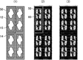
- FIG. 18 is a schematic plan view showing the counter electrode in the FFS mode liquid crystal display device according to Comparative Embodiment 1 examined by the present inventors.
- the counter electrode 14 having the opening 15 is arranged in the upper layer, and the pixel electrode (not shown) is arranged in the lower layer.
- the opening 15 includes a long shape portion 16 and a pair of protrusion portions 17 protruding from the long shape portion 16 to the opposite sides, and has a shape symmetrical to the initial orientation direction 22 of the liquid crystal molecules 21.
- FIG. 18 is a schematic plan view showing the counter electrode in the FFS mode liquid crystal display device according to Comparative Embodiment 1 examined by the present inventors.
- the counter electrode 14 having the opening 15 is arranged in the upper layer, and the pixel electrode (not shown) is arranged in the lower layer.
- the opening 15 includes a long shape portion 16 and a pair of protrusion portions 17 protruding from the long shape portion 16 to the opposite sides, and has a shape symmetrical to the initial
- the liquid crystal molecules 21 can be rotated to form four liquid crystal domains in which the alignment of the liquid crystal molecules 21 is symmetric with each other, and The dark lines between the four liquid crystal domains can be fixed by the oblique electric field in the pair of protrusions 17.
- FIG. 19 is a plan view showing the simulation result of the orientation distribution of the liquid crystal molecules in the on state in the display unit of the liquid crystal display device using the counter electrode of FIG.
- the alignment state of the liquid crystal molecules 21 existing in the central portion of 15 differs depending on the display unit 50. This means that the display units 50 show different transmittances in spite of the same gradation display. Therefore, even when the symmetrical opening 15 including the pair of protrusions 17 is provided, a sufficiently high voltage cannot be applied, and it is difficult to obtain a sufficient transmittance.
- the present invention has been made in view of the above-described situation, and an object of the present invention is to provide a horizontal alignment mode liquid crystal display device capable of increasing the definition and improving the transmittance. is there.
- the present inventors have focused on the shape of the opening of the electrode used for forming the fringe electric field. did. And even if the opening shape of the electrode is not complicated, if the shape satisfies two specific conditions, the electric field at the center of the opening is intentionally distorted to rotate the liquid crystal molecules in a fixed orientation. It was found that the orientation of the liquid crystal molecules can be stabilized at the center of the opening. Specifically, the first straight line that is parallel to the initial alignment direction of the liquid crystal molecules and has the longest length to divide the opening is orthogonal to the initial alignment direction and divides the opening.
- one embodiment of the present invention includes a first substrate, a liquid crystal layer containing liquid crystal molecules, and a second substrate in order, and the first substrate includes the first electrode and the liquid crystal rather than the first electrode.
- a second electrode provided on the layer side, and an insulating film provided between the first electrode and the second electrode, wherein the second electrode has an opening, and the first electrode
- the liquid crystal molecules are aligned in parallel to the first substrate, parallel to the initial alignment direction of the liquid crystal molecules, and
- the contour of the opening is defined by the first straight line having the longest length for dividing the opening and the second straight line orthogonal to the initial orientation direction and having the longest length for dividing the opening. Is divided into four, the average sign of the inclination of each divided contour portion is two adjacent rings. Unlike each of the average of the sign of the slope portion, the average of the outline overall inclination of the opening may be a liquid crystal display device not zero.
- the longer one that divides the opening is the x-axis, and the opening is divided among the first straight line and the second straight line.
- the shorter length is the y-axis, or when the lengths of the first straight line and the second straight line dividing the opening are equal to each other, the first straight line and the second straight line
- the average of the slopes of the contour portions in the first quadrant and the third quadrant is negative, and the contour in the second quadrant and the fourth quadrant
- the average of the slopes of each of the portions may be positive.
- the liquid crystal molecules may have a positive dielectric anisotropy.
- the angle formed by the initial orientation direction and the longitudinal direction of the opening may be 45 degrees or less in plan view.
- the liquid crystal molecules may have negative dielectric anisotropy.
- the angle formed by the initial orientation direction and the longitudinal direction of the opening may be 45 degrees or more in plan view.
- the liquid crystal molecules may rotate in the same direction at the center of the opening.
- the shape of the opening may be the same as the shape when the shape is rotated 180 degrees in a plane parallel to the first substrate.
- the first, second, and third liquid crystal domains exist on the opening, and the first liquid crystal domain is located at the upper right among four regions that are adjacent in the top, bottom, left, and right directions in a plan view. And two domain portions located in the two regions located at the lower left or the lower right and the upper left, respectively, and the two domain portions connected to each other, and a connecting portion located at the center of the opening,
- the second and third liquid crystal domains may be positioned in two regions where the two domain portions are not positioned.
- FIG. 1 It is a cross-sectional schematic diagram of the liquid crystal display device of Embodiment 1, and shows an off state.
- 2 is a schematic plan view of the liquid crystal display device of Embodiment 1.
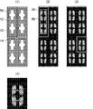
- FIG. FIG. 6 is a diagram showing the relationship between the shape of the opening and the first straight line and the second straight line when liquid crystal molecules having positive dielectric anisotropy are used, and (1) to (5) respectively
- FIG. 4 shows display units of the liquid crystal display devices used in Examples 1 to 5
- FIG. 6 (6) is a diagram for explaining how to obtain the average inclination of the contour portion of the opening.
- FIG. 5 is a diagram showing the relationship between the shape of the opening and the first straight line and the second straight line when liquid crystal molecules having negative dielectric anisotropy are used, and (1) to (5) respectively
- FIG. 4 shows display units of the liquid crystal display devices used in Examples 1 to 5
- FIG. 6 (6) is a diagram for explaining how to obtain the average inclination of the contour portion of the opening.
- FIG. 5 is a diagram showing the relationship between the shape of the opening and the third straight line and the fourth straight line when liquid crystal molecules having positive dielectric anisotropy are used, and (1) to (5) respectively
- the display units of the liquid crystal display devices used in Examples 1 to 5 are shown.
- FIG. 6 is a diagram showing the relationship between the shape of the opening and the third straight line and the fourth straight line when liquid crystal molecules having negative dielectric anisotropy are used, and (1) to (5) respectively The display units of the liquid crystal display devices used in Examples 1 to 5 are shown.
- FIG. 3 is a schematic diagram illustrating alignment control of liquid crystal molecules in an on state in the liquid crystal display device of Embodiment 1.
- 6 is a plan view showing a simulation result of an orientation distribution of liquid crystal molecules in an on state in the liquid crystal display device of Embodiment 1.
- FIG. It is a schematic diagram in the case of forming an opening by a plurality of exposures, (1) is a diagram showing a first exposure portion, and (2) is a diagram showing a second exposure portion.
- Example 1 is the plane schematic diagram which showed the counter electrode and the pixel electrode, (2) shows the simulation result of the orientation distribution of the liquid crystal molecule at the time of 5.5V application. (3) is a plan view showing a simulation result of the orientation distribution of liquid crystal molecules when 6.0 V is applied.
- FIG. 2 is a diagram related to Example 1, (1) is a plan view showing one opening and a pixel electrode in a counter electrode, and (2) is a (1) rotated 180 degrees in a plane parallel to the first substrate.
- (3) is a diagram showing an electric field distribution when a voltage is applied to the opening of (1)
- (4) is a diagram showing a transmittance distribution when a voltage is applied to the opening of (1). is there.
- the liquid crystal display device of Example 2 (1) is a plane schematic diagram of a liquid crystal display device, (2) is a plane schematic diagram which showed the counter electrode and the pixel electrode, (3) is 6. It is the top view which showed the simulation result of the orientation distribution of the liquid crystal molecule at the time of 0V application.
- (1) is a plane schematic diagram of a liquid crystal display device, (2) is a plane schematic diagram which showed the counter electrode and the pixel electrode, (3) is 6.
- (3) is a plan view showing a simulation result of the orientation distribution of liquid crystal molecules when 6.0 V is applied. It is the figure which showed the relationship between the shape of opening and the 1st straight line at the time of using the liquid crystal molecule which has positive dielectric constant anisotropy, (1) is the opening of the opening which has a W-shaped outline part It is a figure and (2) is a figure of the opening which has a mutually parallel outline part. It is the plane schematic diagram which showed the counter electrode in the liquid crystal display device of the FFS mode which concerns on the comparison form 1 which the present inventors examined. It is the top view which showed the simulation result of the orientation distribution of the liquid crystal molecule of the ON state in a display unit of the liquid crystal display device using the counter electrode of FIG.
- FIG. 6 is a schematic plan view of a liquid crystal display device of Comparative Example 1.
- FIG. It is a figure regarding the liquid crystal display device of the comparative example 1, (1) is the plane schematic diagram which showed the counter electrode and the pixel electrode, (2) shows the simulation result of the orientation distribution of the liquid crystal molecule at the time of 4.5V application. (3) is a plan view showing a simulation result of the orientation distribution of liquid crystal molecules when 5.0 V is applied, and (4) is an enlarged plan view of a portion surrounded by a dotted line in (3). It is. It is a figure regarding the comparative example 1, (1) is the top view which showed one opening and pixel electrode in a counter electrode, (2) is the figure which showed the electric field distribution 1 at the time of the voltage application in the opening of (1). (3) is a diagram showing the transmittance distribution 1 in the state of (2), (4) is a diagram showing the electric field distribution 2 when voltage is applied to the opening of (1), 5) is a diagram showing the transmittance distribution 2 in the state of (4).
- FIG. 1 is a schematic cross-sectional view of the liquid crystal display device of Embodiment 1 and shows an off state.
- FIG. 1 shows a cross section taken along the line ab shown in FIG.
- the liquid crystal display device 100 ⁇ / b> A of Embodiment 1 includes a first substrate 10, a liquid crystal layer 20 containing liquid crystal molecules 21, and a second substrate 30 in order.
- the first substrate 10 is a TFT array substrate, and toward the liquid crystal layer 20 side, a first polarizer (not shown), an insulating substrate (for example, a glass substrate) 11, a pixel electrode (first electrode) 12, an insulating layer. (Insulating film) 13 and counter electrode (second electrode) 14 are laminated.
- the second substrate 30 is a color filter substrate, and a second polarizer (not shown), an insulating substrate (for example, a glass substrate) 31, a color filter 32, and an overcoat layer 33 are laminated toward the liquid crystal layer 20 side.
- a first polarizer and the second polarizer is an absorptive polarizer, and has a crossed Nicols arrangement relationship in which the absorption axes are orthogonal to each other.
- the pixel electrode 12 is a planar electrode in which no opening is formed.
- the pixel electrode 12 and the counter electrode 14 are stacked via the insulating layer 13, and the pixel electrode 12 exists under the opening 15 provided in the counter electrode 14. As a result, when a potential difference is generated between the pixel electrode 12 and the counter electrode 14, a fringe electric field is generated around the opening 15 of the counter electrode 14.
- the counter electrode 14 may be formed on almost the entire surface of the first substrate 10 (excluding an opening for forming a fringe electric field).
- the counter electrode 14 may be electrically connected to the external connection terminal at the outer peripheral portion (frame region) of the first substrate 10.
- the liquid crystal molecules 21 may have a negative value of dielectric anisotropy ( ⁇ ) defined by the following formula, or may have a positive value. That is, the liquid crystal molecule 21 may have a negative dielectric anisotropy or a positive dielectric anisotropy. Since the liquid crystal material including the liquid crystal molecules 21 having the negative dielectric anisotropy tends to have a relatively high viscosity, the liquid crystal molecules 21 having the positive dielectric anisotropy are selected from the viewpoint of obtaining high-speed response performance. Including liquid crystal material is superior.
- the means of this embodiment provides the same high-speed response performance by having a low viscosity comparable to that of a liquid crystal material with a positive dielectric anisotropy. It is possible to obtain.
- ⁇ (dielectric constant in the major axis direction)-(dielectric constant in the minor axis direction)
- Liquid crystal molecules 21 in a voltage non-application state where no voltage is applied between the pixel electrode 12 and the counter electrode 14, that is, between the first electrode and the second electrode (hereinafter also simply referred to as a voltage non-application state or an off state). Is controlled in parallel to the first substrate 10. “Parallel” includes not only completely parallel but also a range (substantially parallel) that can be regarded as parallel in the art.
- the pretilt angle (tilt angle in the off state) of the liquid crystal molecules 21 is preferably less than 3 ° with respect to the surface of the first substrate 10, and more preferably less than 1 °.
- the liquid crystal layer 20 In a voltage application state in which a voltage is applied between the pixel electrode 12 and the counter electrode 14, that is, between the first electrode and the second electrode (hereinafter also simply referred to as a voltage application state or an on state), the liquid crystal layer 20. A voltage is applied to the liquid crystal molecules 21, and the orientation of the liquid crystal molecules 21 is controlled by the laminated structure of the pixel electrode 12, the insulating layer 13, and the counter electrode 14 provided on the first substrate 10.
- the pixel electrode 12 is an electrode provided for each display unit
- the counter electrode 14 is an electrode shared by a plurality of display units.
- the “display unit” means an area corresponding to one pixel electrode 12 and may be called “pixel” in the technical field of the liquid crystal display device. When one pixel is divided and driven May be called “sub-pixel”, “dot” or “picture element”.
- the second substrate 30 is not particularly limited, and a color filter substrate generally used in the field of liquid crystal display devices can be used.
- the first substrate 10 and the second substrate 30 are usually bonded together by a sealing material provided so as to surround the periphery of the liquid crystal layer 20, and the liquid crystal layer is formed by the first substrate 10, the second substrate 30, and the sealing material. 20 is held in a predetermined area.
- a sealing material for example, an epoxy resin containing an inorganic filler or an organic filler and a curing agent can be used.
- the liquid crystal display device 100A includes a backlight; an optical film such as a retardation film, a viewing angle widening film, and a brightness enhancement film; TCP (tape carrier package) ), An external circuit such as a PCB (printed wiring board); or a member such as a bezel (frame).
- TCP tape carrier package
- PCB printed wiring board
- frame a member such as a bezel
- the alignment mode of the liquid crystal display device 100A is a fringe electric field switching (FFS) mode.
- FFS fringe electric field switching
- a horizontal alignment film is usually provided on the surface of the first substrate 10 and / or the second substrate 30 on the liquid crystal layer 20 side.
- the horizontal alignment film has a function of aligning liquid crystal molecules 21 existing in the vicinity of the film in parallel to the film surface. Furthermore, according to the horizontal alignment film, the direction of the major axis of the liquid crystal molecules 21 aligned in parallel to the first substrate 10 can be aligned with a specific in-plane orientation.
- the horizontal alignment film is preferably subjected to alignment treatment such as photo-alignment treatment or rubbing treatment.
- the horizontal alignment film may be a film made of an inorganic material or a film made of an organic material.
- the positions of the counter electrode 14 and the pixel electrode 12 may be interchanged. That is, in the stacked structure shown in FIG. 1, the counter electrode 14 is adjacent to the liquid crystal layer 20 via a horizontal alignment film (not shown), but the pixel electrode 12 is liquid crystal via a horizontal alignment film (not shown). It may be adjacent to the layer 20. In this case, the opening 15 is formed not in the counter electrode 14 but in the pixel electrode 12.
- the counter electrode 14 corresponds to the first electrode
- the pixel electrode 12 corresponds to the second electrode.
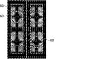
- FIG. 2 is a schematic plan view of the liquid crystal display device according to the first embodiment.
- each opening 15 is formed so as to overlap with the corresponding pixel electrode 12, and the average of the inclination of the contour has a shape that satisfies a specific condition described later.
- These openings 15 are used for forming a fringe electric field (an oblique electric field). Since such an opening 15 does not include a complicated shape, it can be applied to an ultra-high-definition pixel of 800 ppi or more without any problem.
- the opening 15 is preferably arranged for each display unit 50, and is preferably arranged for all the display units 50.
- the planar shape of each display unit 50 is not particularly limited, and examples thereof include a rectangle, a square, and a V shape.
- the initial orientation direction 22 of the liquid crystal molecules 21 is parallel to one polarization axis of the first polarizer and the second polarizer, and orthogonal to the other polarization axis. Therefore, the control method of the liquid crystal display device 100 ⁇ / b> A is a so-called normally black mode in which black display is performed with no voltage applied to the liquid crystal layer 20.
- the initial orientation direction of liquid crystal molecules refers to the orientation direction of liquid crystal molecules in a state in which no voltage is applied between the first electrode and the second electrode, that is, between the pixel electrode and the counter electrode. means. Further, the orientation direction of the liquid crystal molecules means the direction of the major axis of the liquid crystal molecules.
- FIG. 2 shows the case where the liquid crystal molecules 21 have a positive dielectric anisotropy, but the initial alignment direction 22 of the liquid crystal molecules 21 having a negative dielectric anisotropy has a positive dielectric constant difference. It becomes an orientation that rotates 90 degrees with respect to the initial orientation orientation 22 of the liquid crystal molecules 21 having a directivity.
- the drain of the TFT 43 is electrically connected to each pixel electrode 12.
- a gate signal line (scanning wiring) 41 is electrically connected to the gate of the TFT 43, and a source signal line (signal wiring) 42 is electrically connected to the source of the TFT 43. Therefore, on / off of the TFT 43 is controlled in accordance with the scanning signal input to the gate signal line 41.
- the data signal (source voltage) input to the source signal line 42 is supplied to the pixel electrode 12 through the TFT 43.
- the source voltage is applied to the lower pixel electrode 12 via the TFT 43, and the fringe electric field is generated between the counter electrode 14 formed on the upper layer via the insulating film 13 and the pixel electrode 12. Is generated.
- the TFT 43 is preferably formed by forming a channel with IGZO (indium-gallium-zinc-oxygen) which is an oxide semiconductor.
- the openings 15 of the counter electrode 14 are preferably arranged in a line in the row direction and / or the column direction between adjacent display units 50.
- the orientation of the liquid crystal molecules 21 in a voltage application state can be stabilized.
- an opening 15 is formed on one side in the longitudinal direction of the display unit 50, and in a display unit 50 adjacent to the display unit 50, an opening 15 is formed on the other side in the longitudinal direction.
- the openings 15 are alternately arranged in a staggered pattern in the row direction or the column direction between adjacent display units 50 as in the case where the liquid crystal molecules 21 are adjacent, the alignment of the liquid crystal molecules 21 becomes unstable and the response speed decreases.
- the openings 15 are alternately arranged in a staggered pattern in the row direction or the column direction between adjacent display units 50 as in the case where the liquid crystal molecules 21 are adjacent, the alignment of the liquid crystal molecules 21 becomes unstable and the response speed decreases.
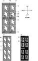
- FIGS. 3 and 4 are diagrams showing the relationship between the shape of the opening and the first straight line and the second straight line when liquid crystal molecules having positive and negative dielectric anisotropy are used, respectively.
- (1) to (5) represent the display units of the liquid crystal display devices used in Examples 1 to 5, respectively
- (6) is a diagram illustrating how to obtain the average of the inclination of the contour portion of the opening. is there.
- the shape of the opening 15 satisfies the following condition. That is, the first straight line 61 that is parallel to the initial alignment direction 22 of the liquid crystal molecules 21 and has the longest length for dividing the opening 15 is orthogonal to the initial alignment direction 22 of the liquid crystal molecules 21. And when the outline of the opening 15 is divided into four with the second straight line 62 having the longest length for dividing the opening 15, (Condition 1) The average sign of the inclination of each divided outline portion is Unlike the sign of the average of the slopes of the two adjacent contour portions, (Condition 2) The average slope of the entire contour of the opening 15 is not zero.
- the average of the slopes of the divided contour portions is obtained as follows.
- the first straight line 61 is the x-axis and the second straight line 62 is used.
- the length of the contour portion projected on the x-axis with the second straight line 62 as the x-axis and the first straight line 61 as the y-axis N straight lines parallel to the y-axis are drawn to divide the length into (n-1) equal parts.
- the average of the gradients of the entire contour is obtained by dividing the sum of the averages of the gradients of the four contour portions divided by four.
- n straight lines parallel to the y-axis include a straight line on the y-axis and a straight line passing through a point farthest from the y-axis of the contour portion.
- positive and negative directions of the x axis and the y axis can be arbitrarily determined with the intersection of the x axis and the y axis as the origin.
- the first straight line 61 and the second straight line 61 and the second straight line 61 regardless of whether the dielectric anisotropy of the liquid crystal molecule 21 is positive or negative.
- Any one of the straight lines 62 may be the x-axis and the other the y-axis.
- n is any positive integer and ideally infinite, but n is preferably any integer from 100 to 300, and any integer from 200 to 300 It is more preferable. Moreover, you may satisfy
- FIG. 17 is a diagram showing the relationship between the shape of the opening and the first straight line when liquid crystal molecules having positive dielectric anisotropy are used, and (1) is a W-shaped contour portion. (2) is a view of an opening having contour portions parallel to each other. There may be a plurality of first straight lines 61 and / or second straight lines 62 with respect to one opening 15, and in that case, all the combinations of the first straight lines 61 and the second straight lines 62 are described above. Condition 1 and condition 2 shall be satisfied. As a specific example of such a case, for example, a case where an opening 15 having a shape as shown in FIGS. 17A and 17B is provided. As shown in FIG.
- the average sign of the inclination of each contour portion is different from the average sign of the inclination of each of the two adjacent contour portions (condition 1), so that the electric field that rotates the liquid crystal molecules 21 in the opposite direction in the adjacent contour portions. It is possible to generate bend-like and splay-like liquid crystal alignments in a narrow region.
- condition 2 since the average inclination of the entire contour of the opening 15 is not zero (condition 2), the shape of the opening 15 is asymmetric with respect to the initial orientation direction 22 of the liquid crystal molecules 21, and the liquid crystal molecules 21 in the center of the opening 15 The rotation can be determined in one direction.
- the average absolute value of the inclination of each contour portion is preferably 0.01 to 2, more preferably 0.05 to 1.8, and still more preferably 0.1 to 1.5. .
- the absolute value of the average inclination of the entire contour of the opening 15 is preferably 0.01 to 2, more preferably 0.02 to 1.5, and still more preferably 0.05 to 1. . If the average inclination of the entire contour of the opening 15 is within the above range, the balance of the liquid crystal domains generated when a voltage is applied can be effectively maintained, and the alignment stability of the liquid crystal molecules 21 can be further improved. Therefore, the response speed can be further improved.
- the longer one that divides the opening 15 is taken as the x-axis, and the first straight line 61 and the second straight line 62 are divided by the opening 15.
- the first straight line 61 and the second straight line 62 are divided by the opening 15.
- the contour of the opening 15 is divided into four contour portions on the first quadrant 71 to the fourth quadrant 74.
- the positive and negative directions of the x-axis and y-axis can be arbitrarily determined with the intersection of the x-axis and y-axis as the origin, and the region where x> 0 and y> 0 is the first quadrant 71, x ⁇ 0 and The region where y> 0 is the second quadrant 72, the region where x ⁇ 0 and y ⁇ 0 is the third quadrant 73, and the region where x> 0 and y ⁇ 0 is the fourth quadrant 74.
- the average of the slopes of the contour portions on the first quadrant 71 and the third quadrant 73 is negative, and the average of the slopes of the contour portions on the second quadrant 72 and the fourth quadrant 74 is positive. Is preferred. Thereby, since the shape of the opening 15 can be further simplified, further high definition can be achieved.
- the dielectric constant has positive dielectric anisotropy.
- the liquid crystal molecules 21 having positive dielectric anisotropy rotate so as to be orthogonal to the inclination of the contour of the opening 15 when a voltage is applied.
- the angle formed between the direction orthogonal to the inclination of the contour of the opening 15 and the initial alignment direction 22 of the liquid crystal molecules 21 having positive dielectric anisotropy is A ⁇ B when A> B. Larger than in some cases. Therefore, in the case of A> B, the liquid crystal molecules 21 having positive dielectric anisotropy can be rotated more greatly from the initial alignment orientation 22 when a voltage is applied, and the transmittance and alignment stability are further improved. It becomes possible.
- the liquid crystal molecules 21 having negative dielectric anisotropy rotate so as to be parallel to the inclination of the contour of the opening 15 when a voltage is applied.
- the angle formed by the azimuth parallel to the inclination of the contour of the opening 15 and the initial orientation azimuth 22 of the liquid crystal molecules 21 having negative dielectric anisotropy is A> B when A ⁇ B. Larger than in some cases. Therefore, in the case of A ⁇ B, the liquid crystal molecules 21 having negative dielectric anisotropy can be rotated more greatly from the initial alignment orientation 22 when a voltage is applied, and the transmittance and alignment stability are further improved. It becomes possible.
- the length A of the opening 15 on the first straight line 61 is the length of the divided portion of the opening 15 divided by the first straight line 61, and the length B of the opening 15 on the second straight line 62. Is the length of the divided portion of the opening 15 divided by the second straight line 62.
- FIGS. 5 and 6 are diagrams showing the relationship between the shape of the opening and the third and fourth straight lines when liquid crystal molecules having positive and negative dielectric anisotropies are used, respectively.
- (1) to (5) represent display units of the liquid crystal display devices used in Examples 1 to 5, respectively.
- the length of the opening 15 that is parallel to the straight line portion of the source signal line 42 (signal wiring) and that is divided by the third straight line 63 that has the longest length for dividing the opening 15 is C, and the gate
- the length of the opening 15 that is parallel to the straight line portion of the signal line 41 (scanning wiring) and is divided by the fourth straight line 64 that has the longest length to divide the opening 15 is D
- the direction of the third straight line 63 or the fourth straight line 64 corresponding to the longer one of C and D is the longitudinal direction of the opening 15. Therefore, in each of the examples shown in FIGS. 5 and 6, the third straight line 63 is the longitudinal direction of the opening 15 in any case.
- the lengths of the openings 15 divided by all the straight lines are compared with each other to determine the longitudinal direction of the openings 15. Shall.
- the angle formed by the initial alignment direction 22 of the liquid crystal molecules 21 and the longitudinal direction of the opening 15 is preferably 45 degrees or less in plan view.
- the angle formed by the initial alignment direction 22 of the liquid crystal molecules 21 and the longitudinal direction of the opening 15 is preferably 45 degrees or more in plan view.
- a ⁇ B can be satisfied, so that the liquid crystal molecules 21 having negative dielectric anisotropy can be rotated more greatly from the initial alignment orientation 22 when a voltage is applied, and the transmittance and alignment stability can be further improved. It becomes possible to improve.
- FIG. 7 is a schematic diagram for explaining alignment control of liquid crystal molecules in an on state in the liquid crystal display device according to the first embodiment.
- FIG. 8 is a plan view showing the simulation result of the orientation distribution of the liquid crystal molecules in the on state in the liquid crystal display device of the first embodiment.
- the liquid crystal molecule 21 since the shape of the opening 15 is asymmetric with respect to the initial orientation direction 22 of the liquid crystal molecule 21, the liquid crystal molecule 21 has the opening 15 in a voltage application state as shown in FIGS. Rotate in the same direction at the center. Therefore, the occurrence of the phenomenon that the alignment state of the liquid crystal molecules 21 differs depending on the display unit 50 when a high voltage is applied can be more reliably reduced.
- the rotation in the same direction means that the liquid crystal molecules 21 rotate to the same side with respect to the initial alignment direction 22.
- the shape of the opening 15 is preferably the same as the shape when the shape is rotated 180 degrees in a plane parallel to the first substrate 10.
- a desired orientation can be realized more efficiently.
- the same shape when rotated 180 degrees means that the shapes when rotated 180 degrees are substantially the same, and the shape of the opening 15 is the same as the first substrate. It means that it overlaps 75% or more with the shape when rotated 180 degrees in a plane parallel to 10.
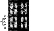
- the first, second and third liquid crystal domains 81 to 83 exist on the opening 15 as shown in FIG.
- two domain portions 81A and two domain portions are connected to each other in two regions located in the upper right and lower left or the lower right and upper left of four regions adjacent to the upper, lower, left, and right sides.
- the second liquid crystal domain 82 and the third liquid crystal domain 83 are located in two regions where the two domain portions 81A are not located, respectively. Yes.
- the first liquid crystal domain 81 includes two domain portions 81A and two domain portions 81A located in two regions located at the lower right and upper left of the four regions adjacent in the top, bottom, left, and right in plan view. And a connecting portion 81B located at the center of the opening 15 is included.
- the second liquid crystal domain 82 and the third liquid crystal domain 83 are respectively located in two regions where the two domain portions 81A are not located.
- the alignment of the liquid crystal molecules in the connecting portion 81B located at the center of the opening 15 can be reliably regulated by the alignment of the liquid crystal molecules in the two domain portions 81A. That is, it is possible to more reliably reduce the occurrence of the phenomenon that the alignment state of the liquid crystal molecules 21 differs depending on the display unit 50 when a high voltage is applied.
- the two domain portions 81A may be located in two regions located at the upper right and the lower left among the four regions adjacent to the upper, lower, left, and right in a plan view.
- the first liquid crystal domain 81, the second liquid crystal domain 82, and the third liquid crystal domain 83 may be generated at least in the white display state, but between the pixel electrode 12 and the counter electrode 14, that is, the first electrode.
- a sufficiently high voltage for example, a voltage of 5.0 V or more
- the relationship between the first to third liquid crystal domains 81 to 83 and the initial orientation direction 22 of the liquid crystal molecules 21 will be examined.
- the angle of the initial alignment direction 22 of the liquid crystal molecules 21 is increased to the direction in which the liquid crystal molecules 21 forming the first liquid crystal domain 81 rotate, the second liquid crystal domain 82 and the third liquid crystal domain are applied when a voltage is applied.
- the region 83 becomes smaller and the balance between the liquid crystal domains is lost. As a result, the distortion caused by the bend-like and splay-like liquid crystal alignment is reduced, so that the effect of high-speed response is reduced.
- the first liquid crystal domain 81 is increased. In this case, there is a possibility that the connection portion 81B is not generated, and in this case, the orientation stability is lowered.
- the angle formed between the initial alignment direction 22 of the liquid crystal molecules 21 having positive dielectric anisotropy and the longitudinal direction of the opening 15 is smaller than 30 degrees. More preferably, it is more preferably less than 20 degrees.
- the angle formed by the initial orientation direction 22 of the liquid crystal molecules 21 having negative dielectric anisotropy and the longitudinal direction of the opening 15 is more preferably more than 60 degrees, and more than 70 degrees. Is more preferable.
- the lower limit of the angle formed by the initial alignment direction 22 of the liquid crystal molecules 21 and the longitudinal direction of the opening 15 is not particularly limited and may be 0 degree or more.
- the upper limit of the angle formed by the initial orientation direction 22 of the liquid crystal molecules 21 and the longitudinal direction of the opening 15 is not particularly limited and may be 90 degrees or less. Good.
- the liquid crystal domain means a region defined by a boundary (dark line) in which the liquid crystal molecules 21 do not rotate from the initial orientation direction 22 when a voltage is applied, and among the four regions adjacent to the top, bottom, left, and right In the liquid crystal domain in this region, the liquid crystal molecules 21 rotate in the opposite direction.
- the top, bottom, left, and right indicate the relative positional relationship between four objects (display units, regions, and the like), and do not mean absolute directions.
- FIG. 9 is a schematic diagram when an opening is formed by a plurality of exposures, where (1) is a first exposure portion and (2) is a second exposure portion.
- means such as exposure can be used.
- the opening 15 having an asymmetric shape as shown in FIG. 7 is formed by a stepper or the like, the opening 15 is formed by one exposure. If it tries to form, an edge part etc. will become dull and it is possible that a desired shape cannot be formed. In such a case, for example, as shown in FIG. 9, a desired shape can be formed by a plurality of exposures.
- the operation of the liquid crystal display device 100A will be described.
- the liquid crystal display device 100A In the off state, no electric field is formed in the liquid crystal layer 20, and the liquid crystal molecules 21 are aligned parallel to the first substrate 10. Since the orientation direction of the liquid crystal molecules 21 is parallel to one absorption axis of the first polarizer and the second polarizer, and the first polarizer and the second polarizer are in a crossed Nicols arrangement, the liquid crystal in the off state
- the display device 100A does not transmit light and performs black display.
- an electric field corresponding to the magnitude of the voltage of the pixel electrode 12 and the counter electrode 14 is formed in the liquid crystal layer 20.
- the opening 15 is formed in the counter electrode 14 provided on the liquid crystal layer 20 side of the pixel electrode 12, whereby a fringe electric field is generated around the opening 15.
- the liquid crystal molecules 21 rotate under the influence of an electric field, and change the orientation azimuth from the off-state orientation azimuth to the on-state orientation azimuth (see FIG. 7). Thereby, the liquid crystal display device 100A in the on state transmits light and white display is performed.
- Example 1 The liquid crystal display device 100A of Example 1 is a specific example of the liquid crystal display device 100A of Embodiment 1 described above, and has the following configuration.
- the pixel pitch in the liquid crystal display device 100A is set to 10.5 ⁇ m ⁇ 31.5 ⁇ m (806 ppi), the plate-like pixel electrodes 12 having no openings such as openings are provided on the insulating substrate 11 in each display unit 50, and the dielectric constant ⁇
- a liquid crystal layer 20 is provided on the counter electrode 14 via an alignment film (not shown).
- the liquid crystal layer 20 has a refractive index anisotropy ( ⁇ n) of 0.111 and an in-plane retardation (Re) of 330 nm.
- ⁇ n refractive index anisotropy
- Re in-plane retardation
- the liquid crystal molecules 21 used in the liquid crystal layer 20 were set to have a viscosity of 70 cps and a dielectric anisotropy ( ⁇ ) of 7 (positive type).
- the liquid crystal molecules 21 are aligned horizontally in parallel with the first substrate 10, and the initial alignment direction 22 of the liquid crystal molecules 21 is 90 in the polarization axis shown in FIG. It was set to be parallel to a straight line indicating 270 degrees and 270 degrees.
- the polarizing plate was in a so-called normally black mode in which black display was performed in the state where no voltage was applied.
- the average of the inclination of the contour portion was obtained in the same manner as the first contour portion. Further, the average of the slopes of the entire contour was obtained by dividing the total sum of the slopes of the first, second, third and fourth contour portions by 4.
- Table 1 below shows the average inclination of the contour portion of the opening 15 used in Example 1 and the average inclination of the entire contour.
- the average of the slopes of the first and third contour portions on the first quadrant 71 and the third quadrant 73 is negative, and the slopes of the second and fourth contour portions on the second quadrant 72 and the fourth quadrant 74 are negative.
- the average was positive, and the average sign of the slope of each contour portion was different from the average sign of the slope of each of the two adjacent contour portions. Moreover, the average of the inclination of the whole outline was not zero.
- FIG. 3A shows the relationship between the shape of the opening 15 used in Example 1 and A and B
- FIG. 5A shows the shape of the opening 15 used in Example 1 and C and D. Shows the relationship.
- Table 2 below shows the lengths A to D and the angle formed between the initial orientation direction 22 of the liquid crystal molecules 21 and the longitudinal direction of the openings 15.
- the opening 15 used in Example 1 was A> B, C> D, and the longitudinal direction of the opening 15 was a direction parallel to the third straight line 63.
- the angle formed between the initial alignment direction 22 of the liquid crystal molecules 21 and the longitudinal direction of the opening 15 (third straight line 63) was 0 degrees in plan view and smaller than 45 degrees.
- the opening 15 used in Example 1 had a shape that overlaps 100% of the area when the shape was rotated 180 degrees in a plane parallel to the first substrate 10.
- FIG. 20 is a schematic plan view of the liquid crystal display device of Comparative Example 1.
- the liquid crystal display device 100A of Comparative Example 1 has the same configuration as the liquid crystal display device 100A of Example 1 except that the shape of the opening 15 of the counter electrode 14 is changed to the shape of FIG.
- the average inclination of the contour of the opening 15 used in Comparative Example 1 was determined in the same manner as in Example 1.
- Table 3 shows the average inclination of the contour portion of the opening 15 used in Comparative Example 1 and the average inclination of the entire contour.
- the average of the slopes of the first and third contour portions on the first quadrant 71 and the third quadrant 73 is negative, and the slopes of the second and fourth contour portions on the second quadrant 72 and the fourth quadrant 74 are negative.
- the average was positive, and the average sign of the slope of each contour portion was different from the average sign of the slope of each of the two adjacent contour portions. Moreover, the average of the inclination of the whole outline was zero.
- FIG. 10 is a diagram relating to the liquid crystal display device 100A of Example 1, (1) is a schematic plan view showing a counter electrode and a pixel electrode, and (2) is an orientation distribution of liquid crystal molecules when 5.5 V is applied. (3) is a plan view showing the simulation result of the orientation distribution of the liquid crystal molecules when 6.0 V is applied.
- FIG. 21 is a diagram related to the liquid crystal display device of Comparative Example 1, (1) is a schematic plan view showing a counter electrode and a pixel electrode, and (2) is an orientation distribution of liquid crystal molecules when 4.5 V is applied.
- the liquid crystal molecules 21 can have the same alignment state in all the display units 50.
- the display unit 50 There was no problem that the transmittance was different. Therefore, in the liquid crystal display device 100A of Example 1, a high voltage can be applied and the transmittance can be increased. Specifically, when a voltage of 6.0 V was applied to the liquid crystal display device 100A of Example 1 during white display, the transmittance was 23.8%. On the other hand, when white voltage was displayed, when a voltage of 4.5 V was applied to the liquid crystal display device 100A of Comparative Example 1, the transmittance was 21.2%. From the above, the liquid crystal display device 100A of Example 1 was able to increase the transmittance by 12.3% as compared with the liquid crystal display device 100A of Comparative Example 1.
- FIG. 11 is a diagram related to Example 1, (1) is a plan view showing one opening and pixel electrode in the counter electrode, and (2) is (1) in a plane parallel to the first substrate. It is the figure rotated 180 degree
- FIG. 11 is a diagram related to Example 1, (1) is a plan view showing one opening and pixel electrode in the counter electrode, and (2) is (1) in a plane parallel to the first substrate. It is the figure rotated 180 degree
- the shape of the opening 15 used in Example 1 is asymmetric with respect to the initial orientation direction 22 of the liquid crystal molecules 21, and the shape is the first substrate 10.
- the shape is the same as when rotated 180 degrees in a plane parallel to the.
- a fringe electric field is generated in four directions when a voltage is applied, and the liquid crystal shown in (a) to (d).
- the liquid crystal molecule 21 was rotated.
- the fringe electric fields in the upper left and lower right directions are stronger than the upper right and lower left fringe electric fields, the liquid crystal molecules 21 in the central portion rotate in the direction of the strong fringe electric fields. This makes it possible to rotate the liquid crystal molecules 21 in a fixed direction at the center of the opening 15 and improve the response speed and transmittance of the liquid crystal display device 100A.
- the shape of the opening 15 is asymmetric with respect to the initial orientation direction 22 of the liquid crystal molecules 21 and the shape is rotated 180 degrees in a plane parallel to the first substrate 10.
- the shape is the same, such an electric field can be generated efficiently.
- the shape of the opening in all other embodiments described later also satisfies this condition.
- Example 22 is a diagram related to Comparative Example 1, (1) is a plan view showing one opening and a pixel electrode in the counter electrode, and (2) is an electric field distribution 1 when voltage is applied to the opening in (1). (3) is a diagram showing a transmittance distribution 1 in the state of (2), and (4) is a diagram showing an electric field distribution 2 when a voltage is applied to the opening of (1). And (5) is a diagram showing the transmittance distribution 2 in the state of (4).
- Comparative Example 1 since the alignment state of the liquid crystal molecules 21 when a high voltage is applied differs depending on the display unit 50, a high voltage cannot be applied, and as a result, the transmittance of the liquid crystal display device 100A is reduced. It will cause a decline.
- FIGS. 12 to 14 are diagrams relating to the liquid crystal display devices of Examples 2 to 4, respectively.
- (1) is a schematic plan view of the liquid crystal display device
- (2) is a plan view showing a counter electrode and a pixel electrode. It is a schematic diagram
- (3) is a plan view showing a simulation result of the orientation distribution of liquid crystal molecules when 6.0 V is applied.
- the liquid crystal display device 100A of the second to fourth embodiments has the same configuration as the liquid crystal display device 100A of the first embodiment, except that the shape of the opening 15 in the counter electrode 14 is changed.
- the counter electrode 14 provided with the opening 15 shown in FIGS. 12 to 14 was used.
- FIGS. 5 (2) to (4) show the examples. The relationship between the shape of the opening 15 used in 2 to 4 and C and D is shown.
- Example 2 and Example 3 The average of the inclination of the contour portion of the opening 15 and the entire contour used in Example 2 and Example 3 was obtained in the same manner as in Example 1.
- the average of the inclination of the contour portion of the opening 15 and the entire contour used in Example 4 was obtained by subtracting 211 straight lines parallel to the y axis that divide the length of each contour portion projected onto the x axis into 210 equal parts. Except for this, it was determined in the same manner as in Example 1.
- the contour portion includes a portion parallel to the first straight line 61 or the second straight line 62 like the opening 15 used in the third embodiment, the inclination of the contour portion is excluded by excluding the parallel portion.
- Table 4 shows the average inclination of the contour portion of the opening 15 and the average inclination of the entire contour used in Examples 2 to 4.
- the average of the slopes of the first and third contour portions on the first quadrant 71 and the third quadrant 73 is negative, and the slopes of the second and fourth contour portions on the second quadrant 72 and the fourth quadrant 74 are negative.
- the average was positive, and the average sign of the slope of each contour portion was different from the average sign of the slope of each of the two adjacent contour portions. Moreover, the average of the inclination of the whole outline was not zero.
- Table 5 below shows the lengths A to D and the angle between the initial orientation direction 22 of the liquid crystal molecules 21 and the longitudinal direction of the openings 15.
- the openings 15 used in Examples 2 to 4 were A> B and C> D, and the longitudinal direction of the openings 15 was parallel to the third straight line 63.
- the angle formed between the initial orientation azimuth 22 and the longitudinal direction of the opening 15 was 0 degrees in plan view and smaller than 45 degrees.
- the opening 15 used in Examples 2 to 4 had a shape that overlaps 100% of the area when the shape was rotated 180 degrees in a plane parallel to the first substrate 10.
- the openings 15 satisfying the above (Condition 1) and (Condition 2) are used.
- a voltage is applied, four liquid crystal domains are formed per one opening 15 in the opening 60, and the liquid crystal molecules 21 are rotated in a predetermined direction in the center of the opening 15 to rotate out of two of the four liquid crystal domains. It became possible to connect the two at the center of the opening 15.
- the liquid crystal display devices 100A of Examples 2 to 4 even when a high voltage of 6.0 V is applied, the liquid crystal molecules 21 can have the same alignment state in all the display units 50, and the transmittance is increased. Became possible. Specifically, when a voltage of 6.0 V is applied during white display, the transmittances in the liquid crystal display devices 100A of Examples 2 to 4 are 24.7%, 24.2%, and 23.6%, respectively. became. Compared with the liquid crystal display device 100A of Comparative Example 1 described above, the liquid crystal display devices 100A of Examples 2 to 4 were able to increase the transmittance by 16%, 14%, and 11%, respectively.
- the liquid crystal display device 100A of the fifth embodiment is the same as the liquid crystal display device 100A of the first embodiment except that the shape of the opening 15 in the counter electrode 14, the initial orientation direction 22 of the liquid crystal molecules 21 and the polarization axes of the pair of polarizers are changed. It has the same configuration as.
- FIG. 15 is a schematic plan view of the liquid crystal display device according to the fifth embodiment.
- the shape of the counter electrode 14 used in Example 5 was the same as that of Comparative Example 1, but the initial orientation direction 22 of the liquid crystal molecules 21 of Example 5 and the polarization axis of the pair of polarizers were 10 degrees from the angle of Comparative Example 1. Tilt.
- FIG. 15 shows the initial alignment direction 22 of the liquid crystal molecules 21.
- FIG. 3 (5) shows the relationship between the shape of the opening 15 used in Example 5 and A and B
- FIG. 5 (5) shows the shape of the opening 15 used in Example 5 and C. And the relationship with D.
- the average of the inclination of the contour portion of the opening 15 and the whole contour used in Example 5 was obtained by subtracting 211 straight lines parallel to the y-axis that divide the length of each contour portion projected onto the x-axis into 210 equal parts. Except for this, it was determined in the same manner as in Example 1. Table 6 below shows the average inclination of the contour portion of the opening 15 used in Example 5 and the average inclination of the entire contour.
- the average of the slopes of the first and third contour portions on the first quadrant 71 and the third quadrant 73 is negative, and the slopes of the second and fourth contour portions on the second quadrant 72 and the fourth quadrant 74 are negative.
- the average was positive, and the average sign of the slope of each contour portion was different from the average sign of the slope of each of the two adjacent contour portions. Moreover, the average of the inclination of the whole outline was not zero.
- Table 7 below shows the lengths A to D and the angle between the initial orientation direction 22 of the liquid crystal molecules 21 and the longitudinal direction of the openings 15.
- the opening 15 used in Example 5 was A> B, C> D, and the longitudinal direction of the opening 15 was a direction parallel to the third straight line 63.
- the angle formed by the initial orientation direction 22 and the longitudinal direction of the opening 15 was 10 degrees in plan view, and was smaller than 45 degrees.
- the opening 15 used in Example 1 had a shape that overlaps 100% of the area when the shape was rotated 180 degrees in a plane parallel to the first substrate 10.
- FIG. 16 is a diagram relating to the liquid crystal display device of Example 5, (1) is a schematic plan view showing a counter electrode and a pixel electrode, and (2) is an orientation distribution of liquid crystal molecules when 5.5 V is applied. It is the top view which showed the simulation result, (3) is the top view which showed the simulation result of the orientation distribution of the liquid crystal molecule at the time of 6.0V application.
- the opening 15 satisfying the above (Condition 1) and (Condition 2) is used, so that a voltage is applied. While forming four liquid crystal domains per opening 15, the liquid crystal molecules 21 are rotated in a predetermined orientation at the center of the opening 15, and two of the four liquid crystal domains are connected at the center of the opening 15. Became possible.
- the liquid crystal molecules 21 can have the same alignment state in all the display units 50.
- the display unit 50 There was no problem that the transmittance was different. Therefore, in the liquid crystal display device 100A of Example 5, a high voltage can be applied and the transmittance can be increased. Specifically, when a voltage of 6.0 V was applied to the liquid crystal display device 100A of Example 5 during white display, the transmittance was 23.9%. On the other hand, when white voltage was displayed, when a voltage of 4.5 V was applied to the liquid crystal display device 100A of Comparative Example 1, the transmittance was 21.2%. From the above, the liquid crystal display device 100A of Example 5 was able to increase the transmittance by 12.7% compared to the liquid crystal display device 100A of Comparative Example 1.
- One embodiment of the present invention includes a first substrate, a liquid crystal layer containing liquid crystal molecules, and a second substrate in order, and the first substrate is closer to the liquid crystal layer than the first electrode and the first electrode.
- a second electrode provided on the first electrode and an insulating film provided between the first electrode and the second electrode, wherein the second electrode has an opening, and the first electrode and the first electrode
- the liquid crystal molecules are aligned parallel to the first substrate, parallel to the initial alignment direction of the liquid crystal molecules, and the opening.
- the outline of the opening is defined by a first straight line having the longest length to divide the opening and a second straight line orthogonal to the initial orientation direction and having the longest length to divide the opening.
- the average sign of the slope of each divided contour portion is calculated for each of the two adjacent contour portions. Unlike the average of the sign of the slope, the average of the outline overall inclination of the opening may be a liquid crystal display device not zero.
- the average sign of the inclination of each contour portion is different from the average sign of each of the two adjacent contour portions, thereby generating an electric field that rotates the liquid crystal molecules 21 in the opposite direction in the adjacent contour portions.
- the average inclination of the entire contour of the opening is not zero, the shape of the opening is asymmetric with respect to the initial alignment direction of the liquid crystal molecules, and the rotation of the liquid crystal molecules at the center of the opening can be determined as one direction. .
- the occurrence of the phenomenon that the alignment state of the liquid crystal molecules differs depending on the display unit when a high voltage is applied can be reduced, and the alignment of the liquid crystal molecules is stabilized even when a high voltage is applied in all display units. Therefore, a sufficiently high voltage can be applied and the transmittance can be improved.
- an opening that satisfies the above conditions can be formed without taking a particularly complicated shape, so that high definition can be realized.
- the longer one that divides the opening is the x-axis, and the opening is divided among the first straight line and the second straight line.
- the shorter length is the y-axis, or when the lengths of the first straight line and the second straight line dividing the opening are equal to each other, the first straight line and the second straight line
- the average of the slopes of the contour portions in the first quadrant and the third quadrant is negative, and the contour in the second quadrant and the fourth quadrant
- the average of the slopes of each of the portions may be positive. According to this aspect, since the shape of the opening can be further simplified, further high definition can be achieved.
- the liquid crystal molecules may have a positive dielectric anisotropy. According to this aspect, liquid crystal molecules having a relatively low viscosity can be used, and the response speed can be further improved.
- the transmittance and the alignment stability can be further improved.
- the angle formed by the initial orientation direction and the longitudinal direction of the opening may be 45 degrees or less in plan view. According to this aspect, the transmittance and the alignment stability can be further improved.
- the liquid crystal molecules may have negative dielectric anisotropy.
- the transmittance and the alignment stability can be further improved.
- the angle formed by the initial orientation direction and the longitudinal direction of the opening may be 45 degrees or more in plan view. According to this aspect, the transmittance and the alignment stability can be further improved.
- the liquid crystal molecules may rotate in the same direction at the center of the opening. According to this aspect, it is possible to more reliably reduce the occurrence of the phenomenon that the alignment state of the liquid crystal molecules differs depending on the display unit when a high voltage is applied.
- the shape of the opening may be the same as the shape when the shape is rotated 180 degrees in a plane parallel to the first substrate. According to this aspect, the desired orientation can be realized more efficiently.
- the first, second, and third liquid crystal domains exist on the opening, and the first liquid crystal domain is located at the upper right among four regions that are adjacent in the top, bottom, left, and right directions in a plan view. And two domain portions located in the two regions located at the lower left or the lower right and the upper left, respectively, and the two domain portions connected to each other, and a connecting portion located at the center of the opening,
- the second and third liquid crystal domains may be positioned in two regions where the two domain portions are not positioned. According to this aspect, it is possible to more reliably reduce the occurrence of the phenomenon that the alignment state of the liquid crystal molecules differs depending on the display unit when a high voltage is applied.
Abstract
Provided is a horizontal orientation mode liquid crystal display that can achieve a high definition, and that can improve transmittance. This liquid crystal display device comprises a first substrate, a liquid crystal layer and a second substrate in that order, wherein the first substrate has a first electrode, a second electrode provided further towards the liquid crystal layer side than the first electrode, and an insulating film between the first electrode and the second electrode. The second electrode has an opening formed therein, and when a voltage is not applied, the liquid crystal molecules are oriented parallel with the first substrate, and in parallel with the initial orientation direction of the liquid crystal molecules, and if the outline of the opening is fragmented into four by a first straight line which fragments the opening to achieve a maximum length and a second straight line that is orthogonal to the direction of initial orientation, and that fragments the opening to achieve a maximum length, the average sign of the inclination of each of the fragmented outline parts is different to the average sign of the inclination of each of the two adjoining outline parts, and the average inclination of the overall outline of the opening is not zero.
Description
本発明は、液晶表示装置に関する。より詳しくは、水平配向モードにおいて高精細な画素を設ける場合に好適な液晶表示装置に関するものである。
The present invention relates to a liquid crystal display device. More specifically, the present invention relates to a liquid crystal display device suitable for providing high-definition pixels in the horizontal alignment mode.
液晶表示装置は、表示のために液晶組成物を利用する表示装置であり、その代表的な表示方式は、一対の基板間に封入された液晶組成物に対して電圧を印加し、印加した電圧に応じて液晶組成物中の液晶分子の配向状態を変化させることにより、光の透過量を制御するものである。このような液晶表示装置は、薄型、軽量及び低消費電力といった特長を活かし、幅広い分野で用いられている。
A liquid crystal display device is a display device that uses a liquid crystal composition for display. A typical display method is to apply a voltage to a liquid crystal composition sealed between a pair of substrates, and apply the applied voltage. The amount of transmitted light is controlled by changing the alignment state of the liquid crystal molecules in the liquid crystal composition according to the above. Such a liquid crystal display device is used in a wide range of fields, taking advantage of its thinness, light weight, and low power consumption.
液晶表示装置の表示方式として、液晶分子の配向を基板面に対して平行な面内で主に回転させることによって制御を行う水平配向モードが、広視野角特性を得やすい等の理由から、注目を集めている。例えば、近年、スマートフォンやタブレットPC向けの液晶表示装置においては、水平配向モードの一種である面内スイッチング(IPS:In-Plane Switching)モードや、フリンジ電界スイッチング(FFS:Fringe Field Switching)モードが広く用いられている。
As a display method for liquid crystal display devices, the horizontal alignment mode, which controls the alignment of liquid crystal molecules mainly in a plane parallel to the substrate surface, is attracting attention because it is easy to obtain wide viewing angle characteristics. Collecting. For example, in recent years, in liquid crystal display devices for smartphones and tablet PCs, in-plane switching (IPS) mode, which is a type of horizontal alignment mode, and fringe field switching (FFS) mode are widely used. It is used.
このような水平配向モードについては、画素の高精細化、透過率の向上、応答速度の向上等による表示品位の向上のための研究開発が続けられている。応答速度を向上するための技術として、例えば、特許文献1には、フリンジ電界を使用する液晶表示装置に関し、第1電極に特定形状の櫛歯部を持たせる技術が開示されている。また、特許文献2には、FFSモードの液晶ディスプレイに関し、2つの直線部分と、2つの直線部分をV字状に連結して形成されたV字部とを含むスリットが形成された電極構造が開示されており、この技術によってプロセスのばらつきに起因する不具合を抑制し、表示性能を向上させることができると説明されている。
With respect to such a horizontal alignment mode, research and development for improving display quality by increasing the definition of pixels, improving transmittance, improving response speed, and the like are continuing. As a technique for improving the response speed, for example, Patent Document 1 discloses a technique in which a first electrode has a comb-shaped portion having a specific shape with respect to a liquid crystal display device using a fringe electric field. Patent Document 2 discloses an electrode structure in which a slit including two straight portions and a V-shaped portion formed by connecting the two straight portions in a V shape is formed with respect to an FFS mode liquid crystal display. It is disclosed that this technique can suppress defects caused by process variations and improve display performance.
水平配向モードは、広視野角を実現できる利点を有するものの、マルチ・ドメイン垂直配向(MVA)モード等の垂直配向モードに比べると応答が遅いという課題があった。特許文献1の技術を用いることで、水平モードにおいても応答速度を向上させることができるが、例えば800ppi以上の超高精細画素では電極の形状が大きく制約され、特許文献1で開示されているような複雑な電極形状をとることが困難である。
Although the horizontal alignment mode has an advantage that a wide viewing angle can be realized, there is a problem that the response is slower than a vertical alignment mode such as a multi-domain vertical alignment (MVA) mode. Although the response speed can be improved even in the horizontal mode by using the technique of Patent Document 1, the shape of the electrode is greatly restricted in, for example, an ultra-high-definition pixel of 800 ppi or more, and is disclosed in Patent Document 1. It is difficult to take a complicated electrode shape.
また、特許文献2では、電極の開口に設けられたV字部の影響より、電圧印加時の液晶分子の配向が上下の2つの領域に分割され、透過率等の表示性能を向上させることができるが、高速化の効果は大きくない。また、更なる高精細化と高透過率化を実現するには未だ改良の余地がある。
Further, in Patent Document 2, due to the influence of the V-shaped portion provided in the opening of the electrode, the alignment of liquid crystal molecules at the time of voltage application is divided into two upper and lower regions, and display performance such as transmittance can be improved. Yes, but the speedup effect is not significant. In addition, there is still room for improvement in order to achieve higher definition and higher transmittance.
そこで、本発明者らは、種々の検討を行った結果、FFSモードの液晶表示装置において、電圧印加時に一定のピッチより小さい範囲で液晶分子を回転させて4つの液晶ドメインを形成し、隣接する液晶ドメインにおける液晶分子を互いに逆方位に回転させることにより、狭い領域内に形成したベンド状及びスプレイ状の液晶配向によって生じる歪みの力を利用して、水平配向モードにおいても高速化及び高精細化を行うことができることを見出した。このとき、4つの液晶ドメインは互いに対称に発生することが理想であるため、上層の電極の開口形状は、液晶分子の初期配向方位に対して対称な形状、例えば四角形の両端部に丸みを持たせた形状や楕円形状が好ましい。そして、この場合、理想的には開口の中央部における液晶分子は回転しない。しかしながら、高電圧を印加すると、4つの液晶ドメインの境界(暗線)を安定化することが困難になり、応答特性が悪化することが分かった。
Therefore, as a result of various studies, the present inventors have formed four liquid crystal domains by rotating liquid crystal molecules in a range smaller than a certain pitch when a voltage is applied in an FFS mode liquid crystal display device, and adjacent to each other. By rotating the liquid crystal molecules in the liquid crystal domain in opposite directions to each other, the strain force generated by the bend-like and splay-like liquid crystal orientations formed in a narrow region is used to increase the speed and resolution in the horizontal alignment mode. Found that can be done. At this time, since it is ideal that the four liquid crystal domains are generated symmetrically with each other, the opening shape of the upper electrode is symmetric with respect to the initial alignment direction of the liquid crystal molecules, for example, roundness at both ends of the square. The shape and oval shape are preferable. In this case, ideally, the liquid crystal molecules at the center of the opening do not rotate. However, it has been found that when a high voltage is applied, it becomes difficult to stabilize the boundary (dark line) between the four liquid crystal domains, and the response characteristics deteriorate.
そこで、高電圧印加時においても暗線を安定化させるため、本発明者らは更なる検討を行った。図18は、本発明者らが検討を行った、比較形態1に係るFFSモードの液晶表示装置における対向電極を示した平面模式図である。図18に示すように、比較形態1に係るFFSモードの液晶表示装置では、開口15を有する対向電極14を上層に配置し、画素電極(図示せず)を下層に配置した。開口15は、長手形状部16と、長手形状部16から互いに反対側に突出した一対の突出部17とから構成され、液晶分子21の初期配向方位22に対して対称な形状とした。図18に示すように、比較形態1に係るFFSモードの液晶表示装置では、液晶分子21を回転させて、互いに液晶分子21の配向が対称な4つの液晶ドメインを形成することができ、かつ、一対の突出部17における斜め方向の電界により、4つの液晶ドメイン間の暗線を固定化することができる。
Therefore, the present inventors have further studied in order to stabilize the dark line even when a high voltage is applied. FIG. 18 is a schematic plan view showing the counter electrode in the FFS mode liquid crystal display device according to Comparative Embodiment 1 examined by the present inventors. As shown in FIG. 18, in the FFS mode liquid crystal display device according to Comparative Example 1, the counter electrode 14 having the opening 15 is arranged in the upper layer, and the pixel electrode (not shown) is arranged in the lower layer. The opening 15 includes a long shape portion 16 and a pair of protrusion portions 17 protruding from the long shape portion 16 to the opposite sides, and has a shape symmetrical to the initial orientation direction 22 of the liquid crystal molecules 21. As shown in FIG. 18, in the FFS mode liquid crystal display device according to Comparative Example 1, the liquid crystal molecules 21 can be rotated to form four liquid crystal domains in which the alignment of the liquid crystal molecules 21 is symmetric with each other, and The dark lines between the four liquid crystal domains can be fixed by the oblique electric field in the pair of protrusions 17.
しかしながら実際は、一対の突出部17を含む対称な形状の開口15が設けられた場合であっても、更に高電圧を印加して液晶分子21の回転が大きくなると、開口15の中央部の液晶分子21の配向が不安定となり、表示単位50によっては開口15の中央部の液晶分子21が回転してしまうことがあった。この原因としては、高電圧印加時、開口15の中央部において電界がわずかに歪んでしまうことや、周囲の液晶分子21の影響を受けて開口15の中央部の液晶分子21の配向のバランスが崩れることが考えられる。図19は、図18の対向電極を用いた液晶表示装置の、表示単位におけるオン状態の液晶分子の配向分布のシミュレーション結果を示した平面図である。開口15の中央部の液晶分子21の回転の有無や程度、方向等の状況は表示単位50毎に異なるため、図19の開口部60中に円形で囲んだ2つの領域が示すように、開口15の中央部に存在する液晶分子21の配向状態が表示単位50によって異なってしまう。これは、同じ階調表示にもかかわらず表示単位50毎に異なる透過率を示すことを意味する。したがって、一対の突出部17を含む対称な形状の開口15が設けられた場合であっても、充分に高い電圧を印加することができず、充分な透過率を得ることが困難であった。
However, in reality, even when the symmetrically shaped opening 15 including the pair of protrusions 17 is provided, when the rotation of the liquid crystal molecules 21 is increased by applying a higher voltage, the liquid crystal molecules at the center of the opening 15 are increased. In some cases, the liquid crystal molecules 21 at the center of the opening 15 may rotate depending on the display unit 50. This is because, when a high voltage is applied, the electric field is slightly distorted in the central portion of the opening 15, and the balance of the alignment of the liquid crystal molecules 21 in the central portion of the opening 15 is influenced by the surrounding liquid crystal molecules 21. It is possible to collapse. FIG. 19 is a plan view showing the simulation result of the orientation distribution of the liquid crystal molecules in the on state in the display unit of the liquid crystal display device using the counter electrode of FIG. Since the presence / absence, degree, direction, and the like of the liquid crystal molecules 21 at the center of the opening 15 are different for each display unit 50, the two openings surrounded by a circle in the opening 60 in FIG. The alignment state of the liquid crystal molecules 21 existing in the central portion of 15 differs depending on the display unit 50. This means that the display units 50 show different transmittances in spite of the same gradation display. Therefore, even when the symmetrical opening 15 including the pair of protrusions 17 is provided, a sufficiently high voltage cannot be applied, and it is difficult to obtain a sufficient transmittance.
本発明は、上記現状に鑑みてなされたものであり、高精細化が可能であり、かつ、透過率を向上させることができる水平配向モードの液晶表示装置を提供することを目的とするものである。
The present invention has been made in view of the above-described situation, and an object of the present invention is to provide a horizontal alignment mode liquid crystal display device capable of increasing the definition and improving the transmittance. is there.
本発明者らは、高精細化が可能であり、かつ、透過率を向上させることができる水平配向モードの液晶表示装置について種々検討した結果、フリンジ電界の形成に用いる電極の開口の形状に着目した。そして、電極の開口形状が複雑でなかったとしても、特定の2つの条件を満たす形状であれば、開口の中央部の電界を意図的に歪ませて、液晶分子を決まった方位に回転させることができ、開口の中央部において液晶分子の配向を安定化させることが可能であることを見出した。詳細には、液晶分子の初期配向方位に対して平行であり、かつ、開口を分断する長さが最長となる第一の直線と、初期配向方位に対して直交し、かつ、開口を分断する長さが最長となる第二の直線とで開口の輪郭を4つに分断した際、(条件1)分断された各輪郭部分の傾きの平均の符号が隣接する2つの輪郭部分の各々の傾きの平均の符号と異なることにより、電圧印可時に狭い領域内にベンド状及びスプレイ状の液晶配向を形成でき、また、(条件2)開口の輪郭全体の傾きの平均がゼロではないことによって、開口の形状が液晶分子の初期配向方位に対して非対称となるため、開口の中央部において、電界を歪ませて液晶分子を決まった方位に回転させることが可能であることを見出した。これにより、高精細化が可能になるとともに、透過率を向上させることが可能となり、上記課題をみごとに解決することができることに想到し、本発明に到達した。
As a result of various studies on a liquid crystal display device in a horizontal alignment mode capable of increasing the definition and improving the transmittance, the present inventors have focused on the shape of the opening of the electrode used for forming the fringe electric field. did. And even if the opening shape of the electrode is not complicated, if the shape satisfies two specific conditions, the electric field at the center of the opening is intentionally distorted to rotate the liquid crystal molecules in a fixed orientation. It was found that the orientation of the liquid crystal molecules can be stabilized at the center of the opening. Specifically, the first straight line that is parallel to the initial alignment direction of the liquid crystal molecules and has the longest length to divide the opening is orthogonal to the initial alignment direction and divides the opening. (Condition 1) When the contour of the opening is divided into four parts by the second straight line having the longest length, (Condition 1) The inclination of each of the two adjacent contour parts is the average sign of the slope of each of the divided contour parts. Bend and splay-like liquid crystal alignment can be formed in a narrow region when voltage is applied, and (condition 2) the average inclination of the entire outline of the opening is not zero, It has been found that the shape of is asymmetric with respect to the initial orientation direction of the liquid crystal molecules, so that the electric field is distorted in the central portion of the opening and the liquid crystal molecules can be rotated to a predetermined orientation. As a result, high definition can be achieved and the transmittance can be improved, and it has been conceived that the above problems can be solved brilliantly, and the present invention has been achieved.
すなわち、本発明の一態様は、第一基板と、液晶分子を含有する液晶層と、第二基板とを順に備え、上記第一基板は、第一電極と、上記第一電極よりも上記液晶層側に設けられた第二電極と、上記第一電極と上記第二電極との間に設けられた絶縁膜とを有し、上記第二電極には開口が形成され、上記第一電極と上記第二電極の間に電圧が印加されない電圧無印加状態において、上記液晶分子は、上記第一基板に対して平行に配向し、上記液晶分子の初期配向方位に対して平行であり、かつ、上記開口を分断する長さが最長となる第一の直線と、上記初期配向方位に対して直交し、かつ、上記開口を分断する長さが最長となる第二の直線とで上記開口の輪郭を4つに分断すると、分断された各輪郭部分の傾きの平均の符号は、隣接する2つの輪郭部分の各々の傾きの平均の符号と異なり、上記開口の上記輪郭全体の傾きの平均は、ゼロではない液晶表示装置であってもよい。
That is, one embodiment of the present invention includes a first substrate, a liquid crystal layer containing liquid crystal molecules, and a second substrate in order, and the first substrate includes the first electrode and the liquid crystal rather than the first electrode. A second electrode provided on the layer side, and an insulating film provided between the first electrode and the second electrode, wherein the second electrode has an opening, and the first electrode In a voltage-free state in which no voltage is applied between the second electrodes, the liquid crystal molecules are aligned in parallel to the first substrate, parallel to the initial alignment direction of the liquid crystal molecules, and The contour of the opening is defined by the first straight line having the longest length for dividing the opening and the second straight line orthogonal to the initial orientation direction and having the longest length for dividing the opening. Is divided into four, the average sign of the inclination of each divided contour portion is two adjacent rings. Unlike each of the average of the sign of the slope portion, the average of the outline overall inclination of the opening may be a liquid crystal display device not zero.
上記第一の直線及び上記第二の直線のうち、上記開口を分断する長さが長い方をx軸とし、かつ、上記第一の直線及び上記第二の直線のうち、上記開口を分断する長さが短い方をy軸としたとき、又は、上記第一の直線及び上記第二の直線の上記開口を分断する長さが互いに等しい場合は、上記第一の直線及び上記第二の直線のいずれか一方をx軸とし、他方をy軸としたとき、第一象限及び第三象限上の輪郭部分の各々の傾きの平均は、負であり、第二象限及び第四象限上の輪郭部分の各々の傾きの平均は、正であってもよい。
Of the first straight line and the second straight line, the longer one that divides the opening is the x-axis, and the opening is divided among the first straight line and the second straight line. When the shorter length is the y-axis, or when the lengths of the first straight line and the second straight line dividing the opening are equal to each other, the first straight line and the second straight line When one of the x axis is the y axis and the other is the y axis, the average of the slopes of the contour portions in the first quadrant and the third quadrant is negative, and the contour in the second quadrant and the fourth quadrant The average of the slopes of each of the portions may be positive.
上記液晶分子は、正の誘電率異方性を有していてもよい。
The liquid crystal molecules may have a positive dielectric anisotropy.
上記第一の直線上における開口の長さをAとし、上記第二の直線上における開口の長さをBとしたとき、A>Bであってもよい。
When the length of the opening on the first straight line is A and the length of the opening on the second straight line is B, A> B may be satisfied.
上記初期配向方位と、上記開口の長手方向とのなす角度は、平面視において、45度以下であってもよい。
The angle formed by the initial orientation direction and the longitudinal direction of the opening may be 45 degrees or less in plan view.
上記液晶分子は、負の誘電率異方性を有していてもよい。
The liquid crystal molecules may have negative dielectric anisotropy.
上記第一の直線上における開口の長さをAとし、上記第二の直線上における開口の長さをBとしたとき、A<Bであってもよい。
When the length of the opening on the first straight line is A and the length of the opening on the second straight line is B, A <B may be satisfied.
上記初期配向方位と、上記開口の長手方向とのなす角度は、平面視において、45度以上であってもよい。
The angle formed by the initial orientation direction and the longitudinal direction of the opening may be 45 degrees or more in plan view.
上記第一電極と上記第二電極の間に電圧が印加された電圧印加状態において、上記液晶分子は、上記開口の中央部において、同一の方位に回転してもよい。
In a voltage application state in which a voltage is applied between the first electrode and the second electrode, the liquid crystal molecules may rotate in the same direction at the center of the opening.
上記開口の形状は、その形状を上記第一基板と平行な平面内で180度回転させた際の形状と同じであってもよい。
The shape of the opening may be the same as the shape when the shape is rotated 180 degrees in a plane parallel to the first substrate.
少なくとも白表示状態において、上記開口上には第一、第二及び第三の液晶ドメインが存在し、上記第一の液晶ドメインは、平面視において、上下左右に隣接する4つの領域のうち、右上及び左下、又は、右下及び左上に位置する2つの領域内にそれぞれ位置する2つのドメイン部分と、上記2つのドメイン部分を連結し、上記開口の中央部に位置する連結部分とを有し、上記第二及び第三の液晶ドメインは、それぞれ、上記2つのドメイン部分が位置しない2つの領域内に位置していてもよい。
At least in the white display state, the first, second, and third liquid crystal domains exist on the opening, and the first liquid crystal domain is located at the upper right among four regions that are adjacent in the top, bottom, left, and right directions in a plan view. And two domain portions located in the two regions located at the lower left or the lower right and the upper left, respectively, and the two domain portions connected to each other, and a connecting portion located at the center of the opening, The second and third liquid crystal domains may be positioned in two regions where the two domain portions are not positioned.
本発明によれば、水平配向モードの液晶表示装置において、高精細化が可能であり、かつ、透過率を向上させることができる。
According to the present invention, in a horizontal alignment mode liquid crystal display device, high definition can be achieved and the transmittance can be improved.
以下、本発明の実施形態について説明する。本発明は、以下の実施形態に限定されるものではなく、本発明の構成を充足する範囲内で、適宜設計変更を行うことが可能である。
なお、以下の説明において、同一部分又は同様な機能を有する部分には同一の符号を異なる図面間で共通して用い、その繰り返しの説明は省略する。
また、実施形態に記載された各構成は、本発明の要旨を逸脱しない範囲において適宜組み合わされてもよいし、変更されてもよい。 Hereinafter, embodiments of the present invention will be described. The present invention is not limited to the following embodiments, and it is possible to appropriately change the design within a range that satisfies the configuration of the present invention.
Note that in the following description, the same portions or portions having similar functions are denoted by the same reference numerals in different drawings, and description thereof is not repeated.
In addition, the configurations described in the embodiments may be appropriately combined or changed without departing from the gist of the present invention.
[実施形態1]
図1~図9に基づき、実施形態1の液晶表示装置について説明する。
図1は、実施形態1の液晶表示装置の断面模式図であり、オフ状態を示している。図1は、図2中に示したa-b線に沿った断面を示している。 [Embodiment 1]
The liquid crystal display device according to the first embodiment will be described with reference to FIGS.
FIG. 1 is a schematic cross-sectional view of the liquid crystal display device ofEmbodiment 1 and shows an off state. FIG. 1 shows a cross section taken along the line ab shown in FIG.
図1~図9に基づき、実施形態1の液晶表示装置について説明する。
図1は、実施形態1の液晶表示装置の断面模式図であり、オフ状態を示している。図1は、図2中に示したa-b線に沿った断面を示している。 [Embodiment 1]
The liquid crystal display device according to the first embodiment will be described with reference to FIGS.
FIG. 1 is a schematic cross-sectional view of the liquid crystal display device of
図1に示したように、実施形態1の液晶表示装置100Aは、第一基板10と、液晶分子21を含有する液晶層20と、第二基板30とを順に備える。第一基板10は、TFTアレイ基板であり、液晶層20側に向かって、第一偏光子(図示省略)、絶縁基板(例えば、ガラス基板)11、画素電極(第一電極)12、絶縁層(絶縁膜)13及び対向電極(第二電極)14が積層された構造を有する。第二基板30は、カラーフィルタ基板であり、液晶層20側に向かって、第二偏光子(図示省略)、絶縁基板(例えば、ガラス基板)31、カラーフィルタ32及びオーバーコート層33が積層された構造を有する。第一偏光子及び第二偏光子は、いずれも吸収型偏光子であり、互いの吸収軸が直交したクロスニコルの配置関係にある。
As shown in FIG. 1, the liquid crystal display device 100 </ b> A of Embodiment 1 includes a first substrate 10, a liquid crystal layer 20 containing liquid crystal molecules 21, and a second substrate 30 in order. The first substrate 10 is a TFT array substrate, and toward the liquid crystal layer 20 side, a first polarizer (not shown), an insulating substrate (for example, a glass substrate) 11, a pixel electrode (first electrode) 12, an insulating layer. (Insulating film) 13 and counter electrode (second electrode) 14 are laminated. The second substrate 30 is a color filter substrate, and a second polarizer (not shown), an insulating substrate (for example, a glass substrate) 31, a color filter 32, and an overcoat layer 33 are laminated toward the liquid crystal layer 20 side. Has a structure. Each of the first polarizer and the second polarizer is an absorptive polarizer, and has a crossed Nicols arrangement relationship in which the absorption axes are orthogonal to each other.
画素電極12は、開口が形成されていない面状電極である。画素電極12と対向電極14とは絶縁層13を介して積層されており、対向電極14に設けられた開口15の下には画素電極12が存在する。これにより、画素電極12と対向電極14の間に電位差を生じさせると、対向電極14の開口15の周囲にフリンジ状の電界が発生する。
The pixel electrode 12 is a planar electrode in which no opening is formed. The pixel electrode 12 and the counter electrode 14 are stacked via the insulating layer 13, and the pixel electrode 12 exists under the opening 15 provided in the counter electrode 14. As a result, when a potential difference is generated between the pixel electrode 12 and the counter electrode 14, a fringe electric field is generated around the opening 15 of the counter electrode 14.
対向電極14は、各表示単位に共通の電位を供給するものであることから、第一基板10のほぼ全面(フリンジ電界形成用の開口部分を除く)に形成されてもよい。対向電極14は、第一基板10の外周部(額縁領域)で外部接続端子と電気的に接続されてもよい。
Since the counter electrode 14 supplies a common potential to each display unit, the counter electrode 14 may be formed on almost the entire surface of the first substrate 10 (excluding an opening for forming a fringe electric field). The counter electrode 14 may be electrically connected to the external connection terminal at the outer peripheral portion (frame region) of the first substrate 10.
画素電極12と対向電極14との間に設けられる絶縁層13としては、例えば、有機膜(誘電率ε=3~4)や、窒化珪素(SiNx)、酸化珪素(SiO2)等の無機膜(誘電率ε=5~7)や、それらの積層膜を用いることができる。
Examples of the insulating layer 13 provided between the pixel electrode 12 and the counter electrode 14 include an organic film (dielectric constant ε = 3 to 4), an inorganic film such as silicon nitride (SiNx), silicon oxide (SiO 2 ), and the like. (Dielectric constant ε = 5 to 7) or a laminated film thereof can be used.
液晶分子21は、下記式で定義される誘電率異方性(Δε)が負の値を有するものであってもよく、正の値を有するものであってもよい。すなわち、液晶分子21は、負の誘電率異方性を有するものであってもよく、正の誘電率異方性であってもよい。負の誘電率異方性を有する液晶分子21を含む液晶材料は相対的に粘度が高い傾向があるため、高速応答性能を得る観点からは、正の誘電率異方性を有する液晶分子21を含む液晶材料が優位である。ただし、誘電率異方性が負の液晶材料であっても、誘電率異方性が正の液晶材料と同程度の低粘度を有することによって、本実施形態の手段で同様の高速応答性能を得ることが可能である。
Δε=(長軸方向の誘電率)-(短軸方向の誘電率) Theliquid crystal molecules 21 may have a negative value of dielectric anisotropy (Δε) defined by the following formula, or may have a positive value. That is, the liquid crystal molecule 21 may have a negative dielectric anisotropy or a positive dielectric anisotropy. Since the liquid crystal material including the liquid crystal molecules 21 having the negative dielectric anisotropy tends to have a relatively high viscosity, the liquid crystal molecules 21 having the positive dielectric anisotropy are selected from the viewpoint of obtaining high-speed response performance. Including liquid crystal material is superior. However, even with a liquid crystal material having a negative dielectric anisotropy, the means of this embodiment provides the same high-speed response performance by having a low viscosity comparable to that of a liquid crystal material with a positive dielectric anisotropy. It is possible to obtain.
Δε = (dielectric constant in the major axis direction)-(dielectric constant in the minor axis direction)
Δε=(長軸方向の誘電率)-(短軸方向の誘電率) The
Δε = (dielectric constant in the major axis direction)-(dielectric constant in the minor axis direction)
画素電極12と対向電極14の間、すなわち第一電極と第二電極の間に電圧が印加されない電圧無印加状態(以下、単に電圧無印加状態、又は、オフ状態とも言う。)における液晶分子21の配向は、第一基板10に対して平行に制御される。「平行」とは、完全な平行だけでなく、当該技術分野において平行と同視可能な範囲(実質的な平行)を含む。液晶分子21のプレチルト角(オフ状態における傾斜角)は、第一基板10の表面に対して3°未満であることが好ましく、1°未満であることがより好ましい。
Liquid crystal molecules 21 in a voltage non-application state where no voltage is applied between the pixel electrode 12 and the counter electrode 14, that is, between the first electrode and the second electrode (hereinafter also simply referred to as a voltage non-application state or an off state). Is controlled in parallel to the first substrate 10. “Parallel” includes not only completely parallel but also a range (substantially parallel) that can be regarded as parallel in the art. The pretilt angle (tilt angle in the off state) of the liquid crystal molecules 21 is preferably less than 3 ° with respect to the surface of the first substrate 10, and more preferably less than 1 °.
画素電極12と対向電極14の間、すなわち第一電極と第二電極の間に電圧が印加された電圧印加状態(以下、単に電圧印加状態、又は、オン状態とも言う。)では、液晶層20に電圧が印加され、液晶分子21の配向は、第一基板10に設けた画素電極12、絶縁層13及び対向電極14の積層構造によって制御される。ここで、画素電極12は、一表示単位毎に設けられる電極であり、対向電極14は、複数の表示単位で共用される電極である。なお、「表示単位」とは、1つの画素電極12に対応する領域を意味し、液晶表示装置の技術分野で「画素」と呼ばれるものであってもよく、一画素を分割して駆動する場合には、「サブ画素(サブピクセル)」、「ドット」又は「絵素」と呼ばれるものであってもよい。
In a voltage application state in which a voltage is applied between the pixel electrode 12 and the counter electrode 14, that is, between the first electrode and the second electrode (hereinafter also simply referred to as a voltage application state or an on state), the liquid crystal layer 20. A voltage is applied to the liquid crystal molecules 21, and the orientation of the liquid crystal molecules 21 is controlled by the laminated structure of the pixel electrode 12, the insulating layer 13, and the counter electrode 14 provided on the first substrate 10. Here, the pixel electrode 12 is an electrode provided for each display unit, and the counter electrode 14 is an electrode shared by a plurality of display units. The “display unit” means an area corresponding to one pixel electrode 12 and may be called “pixel” in the technical field of the liquid crystal display device. When one pixel is divided and driven May be called “sub-pixel”, “dot” or “picture element”.
第二基板30は特に限定されず、液晶表示装置の分野で一般的に用いられるカラーフィルタ基板を用いることができる。オーバーコート層33は、第二基板30の液晶層20側の面を平坦化するものであり、例えば、有機膜(誘電率ε=3~4)を用いることができる。
The second substrate 30 is not particularly limited, and a color filter substrate generally used in the field of liquid crystal display devices can be used. The overcoat layer 33 planarizes the surface of the second substrate 30 on the liquid crystal layer 20 side, and for example, an organic film (dielectric constant ε = 3 to 4) can be used.
第一基板10及び第二基板30は、通常では、液晶層20の周囲を囲むように設けられたシール材によって貼り合わされ、第一の基板10、第二の基板30、及びシール材によって液晶層20が所定の領域に保持される。シール材としては、例えば、無機フィラー又は有機フィラー及び硬化剤を含有するエポキシ樹脂等を用いることができる。
The first substrate 10 and the second substrate 30 are usually bonded together by a sealing material provided so as to surround the periphery of the liquid crystal layer 20, and the liquid crystal layer is formed by the first substrate 10, the second substrate 30, and the sealing material. 20 is held in a predetermined area. As the sealing material, for example, an epoxy resin containing an inorganic filler or an organic filler and a curing agent can be used.
液晶表示装置100Aは、第一基板10、液晶層20及び第二基板30の他に、バックライト;位相差フィルム、視野角拡大フィルム、輝度向上フィルム等の光学フィルム;TCP(テープ・キャリア・パッケージ)、PCB(プリント配線基板)等の外部回路;ベゼル(フレーム)等の部材を備えるものであってもよい。これらの部材については特に限定されず、液晶表示装置の分野において通常使用されるものを用いることができるので、説明を省略する。
In addition to the first substrate 10, the liquid crystal layer 20, and the second substrate 30, the liquid crystal display device 100A includes a backlight; an optical film such as a retardation film, a viewing angle widening film, and a brightness enhancement film; TCP (tape carrier package) ), An external circuit such as a PCB (printed wiring board); or a member such as a bezel (frame). These members are not particularly limited, and those normally used in the field of liquid crystal display devices can be used, and thus the description thereof is omitted.
液晶表示装置100Aの配向モードは、フリンジ電界スイッチング(FFS:Fringe Field Switching)モードである。
The alignment mode of the liquid crystal display device 100A is a fringe electric field switching (FFS) mode.
図1には図示していないが、第一基板10及び/又は第二基板30の液晶層20側の表面には、通常、水平配向膜が設けられる。水平配向膜は、膜近傍に存在する液晶分子21を膜面に対して平行に配向させる機能を有する。更に、水平配向膜によれば、第一基板10に対して平行に配向した液晶分子21の長軸の向きを、特定の面内方位に揃えることができる。水平配向膜は、光配向処理、ラビング処理等の配向処理が施されたものが好適である。水平配向膜は、無機材料からなる膜であってもよいし、有機材料からなる膜であってもよい。
Although not shown in FIG. 1, a horizontal alignment film is usually provided on the surface of the first substrate 10 and / or the second substrate 30 on the liquid crystal layer 20 side. The horizontal alignment film has a function of aligning liquid crystal molecules 21 existing in the vicinity of the film in parallel to the film surface. Furthermore, according to the horizontal alignment film, the direction of the major axis of the liquid crystal molecules 21 aligned in parallel to the first substrate 10 can be aligned with a specific in-plane orientation. The horizontal alignment film is preferably subjected to alignment treatment such as photo-alignment treatment or rubbing treatment. The horizontal alignment film may be a film made of an inorganic material or a film made of an organic material.
なお、対向電極14と画素電極12の位置は入れ替えてもよい。すなわち、図1に示した積層構造では、対向電極14が水平配向膜(図示省略)を介して液晶層20に隣接しているが、画素電極12が水平配向膜(図示省略)を介して液晶層20に隣接していてもよい。この場合には、開口15は、対向電極14ではなく、画素電極12に形成されることになる。また、対向電極14が上記第一電極に対応し、画素電極12が上記第二電極に対応することになる。
Note that the positions of the counter electrode 14 and the pixel electrode 12 may be interchanged. That is, in the stacked structure shown in FIG. 1, the counter electrode 14 is adjacent to the liquid crystal layer 20 via a horizontal alignment film (not shown), but the pixel electrode 12 is liquid crystal via a horizontal alignment film (not shown). It may be adjacent to the layer 20. In this case, the opening 15 is formed not in the counter electrode 14 but in the pixel electrode 12. The counter electrode 14 corresponds to the first electrode, and the pixel electrode 12 corresponds to the second electrode.
図2は、実施形態1の液晶表示装置の平面模式図である。図2に示すように、平面視すると、各開口15は、対応する画素電極12と重なるように形成され、その輪郭の傾きの平均が後述の特定の条件を満たす形状となっている。これらの開口15は、フリンジ電界(斜め電界)の形成に利用される。このような開口15は、複雑な形状を含まないことから、例えば800ppi以上の超高精細画素にも特に問題なく適用することができる。開口15は、一表示単位50毎に配置されることが好ましく、すべての表示単位50に対して配置されることが好ましい。各表示単位50の平面形状は、特に限定されず、例えば、長方形、正方形、V字状等が挙げられる。
FIG. 2 is a schematic plan view of the liquid crystal display device according to the first embodiment. As shown in FIG. 2, when viewed in plan, each opening 15 is formed so as to overlap with the corresponding pixel electrode 12, and the average of the inclination of the contour has a shape that satisfies a specific condition described later. These openings 15 are used for forming a fringe electric field (an oblique electric field). Since such an opening 15 does not include a complicated shape, it can be applied to an ultra-high-definition pixel of 800 ppi or more without any problem. The opening 15 is preferably arranged for each display unit 50, and is preferably arranged for all the display units 50. The planar shape of each display unit 50 is not particularly limited, and examples thereof include a rectangle, a square, and a V shape.
平面視において、液晶分子21の初期配向方位22は、第一偏光子及び第二偏光子の一方の偏光軸と平行であり、他方の偏光軸と直交する。よって、液晶表示装置100Aの制御方式は、液晶層20への電圧無印加状態で黒表示を行う、いわゆるノーマリーブラックモードである。
In plan view, the initial orientation direction 22 of the liquid crystal molecules 21 is parallel to one polarization axis of the first polarizer and the second polarizer, and orthogonal to the other polarization axis. Therefore, the control method of the liquid crystal display device 100 </ b> A is a so-called normally black mode in which black display is performed with no voltage applied to the liquid crystal layer 20.
なお、本明細書において、液晶分子の初期配向方位とは、第一電極と第二電極の間、すなわち画素電極及び対向電極の間に電圧が印加されない電圧無印加状態における液晶分子の配向方位を意味する。また、液晶分子の配向方位とは、液晶分子の長軸の向きを意味する。
In this specification, the initial orientation direction of liquid crystal molecules refers to the orientation direction of liquid crystal molecules in a state in which no voltage is applied between the first electrode and the second electrode, that is, between the pixel electrode and the counter electrode. means. Further, the orientation direction of the liquid crystal molecules means the direction of the major axis of the liquid crystal molecules.
また、図2では、液晶分子21が正の誘電率異方性を有する場合を示しているが、負の誘電率異方性を有する液晶分子21の初期配向方位22は、正の誘電率異方性を有する液晶分子21の初期配向方位22に対して90度回転する方位となる。
FIG. 2 shows the case where the liquid crystal molecules 21 have a positive dielectric anisotropy, but the initial alignment direction 22 of the liquid crystal molecules 21 having a negative dielectric anisotropy has a positive dielectric constant difference. It becomes an orientation that rotates 90 degrees with respect to the initial orientation orientation 22 of the liquid crystal molecules 21 having a directivity.
図2に示したように、各画素電極12には、TFT43のドレインが電気的に接続されている。TFT43のゲートには、ゲート信号線(走査配線)41が電気的に接続され、TFT43のソースには、ソース信号線(信号配線)42が電気的に接続されている。よって、ゲート信号線41に入力された走査信号に応じて、TFT43のオン・オフが制御される。そして、TFT43がオンのときに、ソース信号線42に入力されたデータ信号(ソース電圧)がTFT43を介して画素電極12に供給される。このように、電圧印加状態では、TFT43を介してソース電圧を下層の画素電極12に印加し、絶縁膜13を介して上層に形成されている対向電極14と画素電極12との間でフリンジ電界を発生させる。TFT43は、酸化物半導体であるIGZO(インジウム-ガリウム-亜鉛-酸素)でチャネルを形成したものが好適に用いられる。
As shown in FIG. 2, the drain of the TFT 43 is electrically connected to each pixel electrode 12. A gate signal line (scanning wiring) 41 is electrically connected to the gate of the TFT 43, and a source signal line (signal wiring) 42 is electrically connected to the source of the TFT 43. Therefore, on / off of the TFT 43 is controlled in accordance with the scanning signal input to the gate signal line 41. When the TFT 43 is on, the data signal (source voltage) input to the source signal line 42 is supplied to the pixel electrode 12 through the TFT 43. As described above, in the voltage application state, the source voltage is applied to the lower pixel electrode 12 via the TFT 43, and the fringe electric field is generated between the counter electrode 14 formed on the upper layer via the insulating film 13 and the pixel electrode 12. Is generated. The TFT 43 is preferably formed by forming a channel with IGZO (indium-gallium-zinc-oxygen) which is an oxide semiconductor.
また、図2に示したように、対向電極14の開口15は、隣接する表示単位50同士で、行方向及び/又は列方向に一列に並んで配置されることが好ましい。これにより、電圧印加状態での液晶分子21の配向を安定させることができる。例えば、ある表示単位50では、表示単位50の長手方向の一方の側に開口15が形成され、該表示単位50に隣接する表示単位50では、長手方向の他方の側に開口15が形成されている場合のように、隣接する表示単位50同士で、開口15が行方向又は列方向で互い違いに千鳥格子状に配置されると、液晶分子21の配向が不安定となり、応答速度が低下することがある。
In addition, as shown in FIG. 2, the openings 15 of the counter electrode 14 are preferably arranged in a line in the row direction and / or the column direction between adjacent display units 50. Thereby, the orientation of the liquid crystal molecules 21 in a voltage application state can be stabilized. For example, in a certain display unit 50, an opening 15 is formed on one side in the longitudinal direction of the display unit 50, and in a display unit 50 adjacent to the display unit 50, an opening 15 is formed on the other side in the longitudinal direction. When the openings 15 are alternately arranged in a staggered pattern in the row direction or the column direction between adjacent display units 50 as in the case where the liquid crystal molecules 21 are adjacent, the alignment of the liquid crystal molecules 21 becomes unstable and the response speed decreases. Sometimes.
図3及び図4を用いて開口15の形状を説明する。図3及び図4はそれぞれ、正及び負の誘電率異方性を有する液晶分子を用いた場合における、開口の形状と、第一の直線及び第二の直線との関係を示した図であり、(1)~(5)はそれぞれ、実施例1~5で用いた液晶表示装置の表示単位を表しており、(6)は開口の輪郭部分の傾きの平均の求め方を説明した図である。
The shape of the opening 15 will be described with reference to FIGS. 3 and 4 are diagrams showing the relationship between the shape of the opening and the first straight line and the second straight line when liquid crystal molecules having positive and negative dielectric anisotropy are used, respectively. , (1) to (5) represent the display units of the liquid crystal display devices used in Examples 1 to 5, respectively, and (6) is a diagram illustrating how to obtain the average of the inclination of the contour portion of the opening. is there.
開口15の形状は次の条件を満たす。すなわち、液晶分子21の初期配向方位22に対して平行であり、かつ、開口15を分断する長さが最長となる第一の直線61と、液晶分子21の初期配向方位22に対して直交し、かつ、開口15を分断する長さが最長となる第二の直線62とで開口15の輪郭を4つに分断した際、(条件1)分断された各輪郭部分の傾きの平均の符号は、隣接する2つの輪郭部分の各々の傾きの平均の符号と異なり、(条件2)開口15の輪郭全体の傾きの平均はゼロとはならない。
The shape of the opening 15 satisfies the following condition. That is, the first straight line 61 that is parallel to the initial alignment direction 22 of the liquid crystal molecules 21 and has the longest length for dividing the opening 15 is orthogonal to the initial alignment direction 22 of the liquid crystal molecules 21. And when the outline of the opening 15 is divided into four with the second straight line 62 having the longest length for dividing the opening 15, (Condition 1) The average sign of the inclination of each divided outline portion is Unlike the sign of the average of the slopes of the two adjacent contour portions, (Condition 2) The average slope of the entire contour of the opening 15 is not zero.
本明細書において、分断された各輪郭部分の傾きの平均は、各々、以下のようにして求める。
図3(6)及び図4(6)に示したように、まず、正の誘電率異方性を有する液晶分子21を用いる場合は、第一の直線61をx軸、第二の直線62をy軸とし、負の誘電率異方性を有する液晶分子21を用いる場合は、第二の直線62をx軸、第一の直線61をy軸とし、x軸に投影した輪郭部分の長さを(n-1)等分する、y軸に平行なn本の直線を引く。そして、それらの直線と輪郭部分との交点(1つの直線上に複数の交点がある場合は、全ての交点)で微分して各々の点における傾きを求める。それらの傾きの総和を交点の総数で除したものを分断された輪郭部分の傾きの平均とする。また、本明細書において、輪郭全体の傾きの平均とは、分断された4つの輪郭部分の傾きの平均の総和を4で除したものである。 In the present specification, the average of the slopes of the divided contour portions is obtained as follows.
As shown in FIGS. 3 (6) and 4 (6), when theliquid crystal molecules 21 having positive dielectric anisotropy are used, the first straight line 61 is the x-axis and the second straight line 62 is used. Is the y-axis and the liquid crystal molecules 21 having negative dielectric anisotropy are used, the length of the contour portion projected on the x-axis with the second straight line 62 as the x-axis and the first straight line 61 as the y-axis N straight lines parallel to the y-axis are drawn to divide the length into (n-1) equal parts. Then, differentiation is performed at intersections between the straight lines and the contour portion (all intersections when there are a plurality of intersections on one straight line) to obtain inclinations at the respective points. The sum of the slopes divided by the total number of intersections is taken as the average slope of the divided contour portions. Further, in this specification, the average of the gradients of the entire contour is obtained by dividing the sum of the averages of the gradients of the four contour portions divided by four.
図3(6)及び図4(6)に示したように、まず、正の誘電率異方性を有する液晶分子21を用いる場合は、第一の直線61をx軸、第二の直線62をy軸とし、負の誘電率異方性を有する液晶分子21を用いる場合は、第二の直線62をx軸、第一の直線61をy軸とし、x軸に投影した輪郭部分の長さを(n-1)等分する、y軸に平行なn本の直線を引く。そして、それらの直線と輪郭部分との交点(1つの直線上に複数の交点がある場合は、全ての交点)で微分して各々の点における傾きを求める。それらの傾きの総和を交点の総数で除したものを分断された輪郭部分の傾きの平均とする。また、本明細書において、輪郭全体の傾きの平均とは、分断された4つの輪郭部分の傾きの平均の総和を4で除したものである。 In the present specification, the average of the slopes of the divided contour portions is obtained as follows.
As shown in FIGS. 3 (6) and 4 (6), when the
ただし、傾きが0又は無限大になる点については、配向制御に寄与しないため除外する。なお、y軸に平行なn本の直線には、y軸上の直線と、当該輪郭部分のy軸から最も遠い点を通る直線が含まれることとする。また、x軸及びy軸の交点を原点として、x軸及びy軸の正負の向きは任意に決めることができる。更に、第一の直線61及び第二の直線62の開口15を分断する長さが互いに等しい場合は、液晶分子21の誘電率異方性の正負に関わらず、第一の直線61及び第二の直線62のいずれか一方をx軸とし、他方をy軸とすればよい。
However, points where the slope becomes 0 or infinity are excluded because they do not contribute to the orientation control. Note that the n straight lines parallel to the y-axis include a straight line on the y-axis and a straight line passing through a point farthest from the y-axis of the contour portion. Further, the positive and negative directions of the x axis and the y axis can be arbitrarily determined with the intersection of the x axis and the y axis as the origin. Further, when the lengths for dividing the opening 15 of the first straight line 61 and the second straight line 62 are equal to each other, the first straight line 61 and the second straight line 61 and the second straight line 61 regardless of whether the dielectric anisotropy of the liquid crystal molecule 21 is positive or negative. Any one of the straight lines 62 may be the x-axis and the other the y-axis.
nは任意の正の整数であり、理想的には無限大であるが、nは100~300のうちのいずれかの整数であることが好ましく、200~300のうちのいずれかの整数であることがより好ましい。また、これらの数値範囲の全てのnについて上記条件1及び条件2を満たしてもよい。
n is any positive integer and ideally infinite, but n is preferably any integer from 100 to 300, and any integer from 200 to 300 It is more preferable. Moreover, you may satisfy | fill the said conditions 1 and conditions 2 about all the n of these numerical ranges.
図17は、正の誘電率異方性を有する液晶分子を用いた場合における、開口の形状と、第一の直線との関係を示した図であり、(1)はW字状の輪郭部分を有する開口の図であり、(2)は互いに平行な輪郭部分を有する開口の図である。1つの開口15に対して第一の直線61及び/又は第二の直線62が複数本存在してもよく、その場合は、第一の直線61及び第二の直線62の全ての組み合わせについて上記条件1及び条件2を満たすものとする。このような場合の具体例としては、例えば、図17(1)及び(2)に示すような形状の開口15が設けられた場合が挙げられる。なお、図17(2)に示すように、第一の直線61が配置され得る開口15の対向部分が、互いに平行で、かつ、初期配向方位22に対して垂直又は平行でない場合は、該対向部分の両端と中央を通る少なくとも3本の第一の直線61と第二の直線62との全ての組み合わせについて上記条件1及び2を満たすものとする。第二の直線62が配置され得る開口15の対向部分が、互いに平行で、かつ、初期配向方位22に対して垂直又は平行でない場合も同様とする。
FIG. 17 is a diagram showing the relationship between the shape of the opening and the first straight line when liquid crystal molecules having positive dielectric anisotropy are used, and (1) is a W-shaped contour portion. (2) is a view of an opening having contour portions parallel to each other. There may be a plurality of first straight lines 61 and / or second straight lines 62 with respect to one opening 15, and in that case, all the combinations of the first straight lines 61 and the second straight lines 62 are described above. Condition 1 and condition 2 shall be satisfied. As a specific example of such a case, for example, a case where an opening 15 having a shape as shown in FIGS. 17A and 17B is provided. As shown in FIG. 17 (2), when the opposing portions of the opening 15 where the first straight line 61 can be arranged are parallel to each other and not perpendicular or parallel to the initial orientation direction 22, the opposing portions The above conditions 1 and 2 are satisfied for all combinations of at least three first straight lines 61 and second straight lines 62 passing through both ends and the center of the portion. The same applies to the case where the opposing portions of the opening 15 in which the second straight line 62 can be arranged are parallel to each other and not perpendicular or parallel to the initial orientation direction 22.
各輪郭部分の傾きの平均の符号が、隣接する2つの輪郭部分の各々の傾きの平均の符号と異なることにより(条件1)、隣接する輪郭部分において、液晶分子21を逆方位に回転させる電界を発生させることができ、狭い領域内にベンド状及びスプレイ状の液晶配向を形成することが可能となる。また、開口15の輪郭全体の傾きの平均はゼロではないため(条件2)、開口15の形状は液晶分子21の初期配向方位22に対して非対称となり、開口15の中央部における液晶分子21の回転を1方位に決定することができる。これにより、高電圧印加時に表示単位50によって液晶分子21の配向状態が異なるという現象の発生を低減でき、全ての表示単位50で高電圧印加時にも液晶分子21の配向が安定する。そのため、充分に高い電圧を印加でき、透過率を向上させることが可能となる。
The average sign of the inclination of each contour portion is different from the average sign of the inclination of each of the two adjacent contour portions (condition 1), so that the electric field that rotates the liquid crystal molecules 21 in the opposite direction in the adjacent contour portions. It is possible to generate bend-like and splay-like liquid crystal alignments in a narrow region. In addition, since the average inclination of the entire contour of the opening 15 is not zero (condition 2), the shape of the opening 15 is asymmetric with respect to the initial orientation direction 22 of the liquid crystal molecules 21, and the liquid crystal molecules 21 in the center of the opening 15 The rotation can be determined in one direction. Thereby, the occurrence of the phenomenon that the alignment state of the liquid crystal molecules 21 differs depending on the display unit 50 when a high voltage is applied can be reduced, and the alignment of the liquid crystal molecules 21 is stabilized even when a high voltage is applied in all the display units 50. Therefore, a sufficiently high voltage can be applied and the transmittance can be improved.
各輪郭部分の傾きの平均の絶対値は、0.01~2であることが好ましく、0.05~1.8であることがより好ましく、0.1~1.5であることが更に好ましい。
The average absolute value of the inclination of each contour portion is preferably 0.01 to 2, more preferably 0.05 to 1.8, and still more preferably 0.1 to 1.5. .
開口15の輪郭全体の傾きの平均の絶対値は、0.01~2であることが好ましく、0.02~1.5であることがより好ましく、0.05~1であることが更に好ましい。開口15の輪郭全体の傾きの平均が上記の範囲であると、電圧印加時に発生する液晶ドメインのバランスを効果的に維持できるため、液晶分子21の配向安定性を更に高めることができる。そのため、応答速度をより向上させることが可能となる。
The absolute value of the average inclination of the entire contour of the opening 15 is preferably 0.01 to 2, more preferably 0.02 to 1.5, and still more preferably 0.05 to 1. . If the average inclination of the entire contour of the opening 15 is within the above range, the balance of the liquid crystal domains generated when a voltage is applied can be effectively maintained, and the alignment stability of the liquid crystal molecules 21 can be further improved. Therefore, the response speed can be further improved.
第一の直線61及び第二の直線62のうち、開口15を分断する長さが長い方をx軸とし、かつ、第一の直線61及び第二の直線62のうち、開口15を分断する長さが短い方をy軸としたとき、又は、第一の直線61及び第二の直線62の開口15を分断する長さが互いに等しい場合は、第一の直線61及び第二の直線62のいずれか一方をx軸とし、他方をy軸としたとき、開口15の輪郭は、第一象限71~第四象限74上の4つの輪郭部分に分断される。なお、x軸及びy軸の交点を原点として、x軸及びy軸の正負の向きは任意に決めることができ、x>0及びy>0である領域が第一象限71、x<0及びy>0である領域が第二象限72、x<0及びy<0である領域が第三象限73、x>0及びy<0である領域が第四象限74である。
Of the first straight line 61 and the second straight line 62, the longer one that divides the opening 15 is taken as the x-axis, and the first straight line 61 and the second straight line 62 are divided by the opening 15. When the shorter length is taken as the y-axis, or when the lengths that divide the openings 15 of the first straight line 61 and the second straight line 62 are equal to each other, the first straight line 61 and the second straight line 62 When one of these is the x-axis and the other is the y-axis, the contour of the opening 15 is divided into four contour portions on the first quadrant 71 to the fourth quadrant 74. The positive and negative directions of the x-axis and y-axis can be arbitrarily determined with the intersection of the x-axis and y-axis as the origin, and the region where x> 0 and y> 0 is the first quadrant 71, x <0 and The region where y> 0 is the second quadrant 72, the region where x <0 and y <0 is the third quadrant 73, and the region where x> 0 and y <0 is the fourth quadrant 74.
第一象限71及び第三象限73上の輪郭部分の各々の傾きの平均は、負であり、第二象限72及び第四象限74上の輪郭部分の各々の傾きの平均は、正であることが好ましい。これにより、開口15の形状を更に簡便なものとすることができるため、更なる高精細化が可能となる。
The average of the slopes of the contour portions on the first quadrant 71 and the third quadrant 73 is negative, and the average of the slopes of the contour portions on the second quadrant 72 and the fourth quadrant 74 is positive. Is preferred. Thereby, since the shape of the opening 15 can be further simplified, further high definition can be achieved.
第一の直線61上における開口15の長さをAとし、第二の直線62上における開口15の長さをBとしたとき、A>Bである場合は正の誘電率異方性を有する液晶分子21を用いることが好ましい。正の誘電率異方性を有する液晶分子21は、電圧を印加した際に、開口15の輪郭の傾きに対して直交するように回転する。開口15の輪郭の傾きに対して直交する方位と、正の誘電率異方性を有する液晶分子21の初期配向方位22とがなす角度は、A>Bである場合の方がA<Bである場合と比較して大きくなる。したがって、A>Bである場合の方が電圧印加時に正の誘電率異方性を有する液晶分子21を初期配向方位22からより大きく回転させることができ、透過率及び配向安定性をより向上させることが可能となる。
When the length of the opening 15 on the first straight line 61 is A and the length of the opening 15 on the second straight line 62 is B, when A> B, the dielectric constant has positive dielectric anisotropy. It is preferable to use liquid crystal molecules 21. The liquid crystal molecules 21 having positive dielectric anisotropy rotate so as to be orthogonal to the inclination of the contour of the opening 15 when a voltage is applied. The angle formed between the direction orthogonal to the inclination of the contour of the opening 15 and the initial alignment direction 22 of the liquid crystal molecules 21 having positive dielectric anisotropy is A <B when A> B. Larger than in some cases. Therefore, in the case of A> B, the liquid crystal molecules 21 having positive dielectric anisotropy can be rotated more greatly from the initial alignment orientation 22 when a voltage is applied, and the transmittance and alignment stability are further improved. It becomes possible.
他方、A<Bである場合は負の誘電率異方性を有する液晶分子21を用いることが好ましい。負の誘電率異方性を有する液晶分子21は、電圧を印加した際に、開口15の輪郭の傾きに対して平行となるように回転する。開口15の輪郭の傾きに対して平行な方位と、負の誘電率異方性を有する液晶分子21の初期配向方位22とがなす角度は、A<Bである場合の方がA>Bである場合と比較して大きくなる。したがって、A<Bである場合の方が電圧印加時に負の誘電率異方性を有する液晶分子21を初期配向方位22からより大きく回転させることができ、透過率及び配向安定性をより向上させることが可能となる。
On the other hand, when A <B, it is preferable to use the liquid crystal molecules 21 having negative dielectric anisotropy. The liquid crystal molecules 21 having negative dielectric anisotropy rotate so as to be parallel to the inclination of the contour of the opening 15 when a voltage is applied. The angle formed by the azimuth parallel to the inclination of the contour of the opening 15 and the initial orientation azimuth 22 of the liquid crystal molecules 21 having negative dielectric anisotropy is A> B when A <B. Larger than in some cases. Therefore, in the case of A <B, the liquid crystal molecules 21 having negative dielectric anisotropy can be rotated more greatly from the initial alignment orientation 22 when a voltage is applied, and the transmittance and alignment stability are further improved. It becomes possible.
なお、第一の直線61上における開口15の長さAは、第一の直線61で分断された開口15の分断部の長さであり、第二の直線62上における開口15の長さBは、第二の直線62で分断された開口15の分断部の長さである。
The length A of the opening 15 on the first straight line 61 is the length of the divided portion of the opening 15 divided by the first straight line 61, and the length B of the opening 15 on the second straight line 62. Is the length of the divided portion of the opening 15 divided by the second straight line 62.
次に、図5及び図6を用いて、開口15の長手方向と液晶分子21の初期配向方位22との好ましい関係について説明する。図5及び図6はそれぞれ、正及び負の誘電率異方性を有する液晶分子を用いた場合における、開口の形状と、第三の直線及び第四の直線との関係を示した図であり、(1)~(5)はそれぞれ、実施例1~5で用いた液晶表示装置の表示単位を表している。
Next, a preferable relationship between the longitudinal direction of the opening 15 and the initial orientation direction 22 of the liquid crystal molecules 21 will be described with reference to FIGS. 5 and 6. FIGS. 5 and 6 are diagrams showing the relationship between the shape of the opening and the third and fourth straight lines when liquid crystal molecules having positive and negative dielectric anisotropies are used, respectively. , (1) to (5) represent display units of the liquid crystal display devices used in Examples 1 to 5, respectively.
まず、開口15の長手方向の決め方を説明する。ソース信号線42(信号配線)の直線部分に対して平行であり、かつ、開口15を分断する長さが最長となる第三の直線63で分断された開口15の長さをCとし、ゲート信号線41(走査配線)の直線部分に対して平行であり、かつ、開口15を分断する長さが最長となる第四の直線64で分断された開口15の長さをDとした時、C及びDのうち長い方に対応する第三の直線63又は第四の直線64の方向を開口15の長手方向とする。したがって、図5及び図6に示した例では、いずれの場合も第三の直線63が開口15の長手方向となる。なお、第三の直線63及び/又は第四の直線64が複数本存在する場合は、それらの全ての直線で分断された開口15の長さを互いに比較して開口15の長手方向を決定するものとする。
First, how to determine the longitudinal direction of the opening 15 will be described. The length of the opening 15 that is parallel to the straight line portion of the source signal line 42 (signal wiring) and that is divided by the third straight line 63 that has the longest length for dividing the opening 15 is C, and the gate When the length of the opening 15 that is parallel to the straight line portion of the signal line 41 (scanning wiring) and is divided by the fourth straight line 64 that has the longest length to divide the opening 15 is D, The direction of the third straight line 63 or the fourth straight line 64 corresponding to the longer one of C and D is the longitudinal direction of the opening 15. Therefore, in each of the examples shown in FIGS. 5 and 6, the third straight line 63 is the longitudinal direction of the opening 15 in any case. When there are a plurality of third straight lines 63 and / or fourth straight lines 64, the lengths of the openings 15 divided by all the straight lines are compared with each other to determine the longitudinal direction of the openings 15. Shall.
液晶分子21が正の誘電率異方性を有する場合、液晶分子21の初期配向方位22と、開口15の長手方向とのなす角度は、平面視において、45度以下であることが好ましい。これにより、A>Bとすることができるため、電圧印加時に正の誘電率異方性を有する液晶分子21を初期配向方位22からより大きく回転させることができ、透過率及び配向安定性をより向上させることが可能となる。
When the liquid crystal molecules 21 have positive dielectric anisotropy, the angle formed by the initial alignment direction 22 of the liquid crystal molecules 21 and the longitudinal direction of the opening 15 is preferably 45 degrees or less in plan view. Thereby, since A> B, the liquid crystal molecules 21 having positive dielectric anisotropy can be rotated more greatly from the initial orientation direction 22 when a voltage is applied, and the transmittance and orientation stability can be further improved. It becomes possible to improve.
液晶分子21が負の誘電率異方性を有する場合、液晶分子21の初期配向方位22と、開口15の長手方向とのなす角度は、平面視において、45度以上であることが好ましい。これにより、A<Bとすることができため、電圧印加時に負の誘電率異方性を有する液晶分子21を初期配向方位22からより大きく回転させることができ、透過率及び配向安定性をより向上させることが可能となる。
When the liquid crystal molecules 21 have negative dielectric anisotropy, the angle formed by the initial alignment direction 22 of the liquid crystal molecules 21 and the longitudinal direction of the opening 15 is preferably 45 degrees or more in plan view. As a result, A <B can be satisfied, so that the liquid crystal molecules 21 having negative dielectric anisotropy can be rotated more greatly from the initial alignment orientation 22 when a voltage is applied, and the transmittance and alignment stability can be further improved. It becomes possible to improve.
液晶分子21の初期配向方位22と開口15の長手方向とのなす角度が45度である場合、正負いずれの誘電率異方性を有する液晶分子を用いても同様の効果が得られる。
When the angle formed by the initial alignment direction 22 of the liquid crystal molecules 21 and the longitudinal direction of the opening 15 is 45 degrees, the same effect can be obtained even if liquid crystal molecules having either positive or negative dielectric anisotropy are used.
図7は、実施形態1の液晶表示装置における、オン状態の液晶分子の配向制御を説明する模式図である。図8は、実施形態1の液晶表示装置における、オン状態の液晶分子の配向分布のシミュレーション結果を示した平面図である。
FIG. 7 is a schematic diagram for explaining alignment control of liquid crystal molecules in an on state in the liquid crystal display device according to the first embodiment. FIG. 8 is a plan view showing the simulation result of the orientation distribution of the liquid crystal molecules in the on state in the liquid crystal display device of the first embodiment.
本実施形態によれば、開口15の形状は液晶分子21の初期配向方位22に対して非対称であるため、図7及び図8に示すように、電圧印加状態において、液晶分子21は、開口15の中央部において、同一の方位に回転する。したがって、高電圧印加時に表示単位50によって液晶分子21の配向状態が異なるという現象の発生をより確実に低減することができる。なお、同一の方位に回転とは、液晶分子21が初期配向方位22に対して同じ側に回転することを意味する。
According to the present embodiment, since the shape of the opening 15 is asymmetric with respect to the initial orientation direction 22 of the liquid crystal molecule 21, the liquid crystal molecule 21 has the opening 15 in a voltage application state as shown in FIGS. Rotate in the same direction at the center. Therefore, the occurrence of the phenomenon that the alignment state of the liquid crystal molecules 21 differs depending on the display unit 50 when a high voltage is applied can be more reliably reduced. The rotation in the same direction means that the liquid crystal molecules 21 rotate to the same side with respect to the initial alignment direction 22.
開口15の形状は、その形状を第一基板10と平行な平面内で180度回転させた際の形状と同じであることが好ましい。このような形状の開口15を用いることにより、より効率的に所望の配向を実現することができる。ここで、180度回転させた際の形状が同じであるとは、180度回転させた際の形状が実質的に同一であることを意味し、開口15の形状は、その形状を第一基板10と平行な平面内で180度回転させた際の形状と75%以上重なることを意味する。
The shape of the opening 15 is preferably the same as the shape when the shape is rotated 180 degrees in a plane parallel to the first substrate 10. By using the opening 15 having such a shape, a desired orientation can be realized more efficiently. Here, the same shape when rotated 180 degrees means that the shapes when rotated 180 degrees are substantially the same, and the shape of the opening 15 is the same as the first substrate. It means that it overlaps 75% or more with the shape when rotated 180 degrees in a plane parallel to 10.
少なくとも白(最高階調)表示状態において、開口15上には、図8に示したように、第一、第二及び第三の液晶ドメイン81~83が存在し、第一の液晶ドメイン81は、平面視において、上下左右に隣接する4つの領域のうち、右上及び左下、又は、右下及び左上に位置する2つの領域内にそれぞれ位置する2つのドメイン部分81Aと、2つのドメイン部分を連結し、開口の中央部に位置する連結部分81Bとを有し、第二の液晶ドメイン82及び第三の液晶ドメイン83は、それぞれ、2つのドメイン部分81Aが位置しない2つの領域内に位置している。
At least in the white (highest gradation) display state, the first, second and third liquid crystal domains 81 to 83 exist on the opening 15 as shown in FIG. In a plan view, two domain portions 81A and two domain portions are connected to each other in two regions located in the upper right and lower left or the lower right and upper left of four regions adjacent to the upper, lower, left, and right sides. The second liquid crystal domain 82 and the third liquid crystal domain 83 are located in two regions where the two domain portions 81A are not located, respectively. Yes.
すなわち、少なくとも白表示状態において、図7及び図8に示すように、開口(図8では図示せず)15上には第一の液晶ドメイン81、第二の液晶ドメイン82及び第三の液晶ドメイン83が発生している。第一の液晶ドメイン81は、平面視において、上下左右に隣接する4つの領域のうち、右下及び左上に位置する2つの領域内にそれぞれ位置する2つのドメイン部分81Aと、2つのドメイン部分81Aを連結し、開口15の中央部に位置する連結部分81Bとを含んでいる。第二の液晶ドメイン82及び第三の液晶ドメイン83は、それぞれ、2つのドメイン部分81Aが位置しない2つの領域内に位置している。
That is, at least in the white display state, as shown in FIGS. 7 and 8, the first liquid crystal domain 81, the second liquid crystal domain 82, and the third liquid crystal domain are formed on the opening (not shown in FIG. 8) 15. 83 has occurred. The first liquid crystal domain 81 includes two domain portions 81A and two domain portions 81A located in two regions located at the lower right and upper left of the four regions adjacent in the top, bottom, left, and right in plan view. And a connecting portion 81B located at the center of the opening 15 is included. The second liquid crystal domain 82 and the third liquid crystal domain 83 are respectively located in two regions where the two domain portions 81A are not located.
これにより、開口15の中央部に位置する連結部分81Bにおける液晶分子の配向を2つのドメイン部分81Aにおける液晶分子の配向によって確実に規制することができる。すなわち、高電圧印加時に表示単位50によって液晶分子21の配向状態が異なるという現象の発生をより確実に低減することができる。なお、2つのドメイン部分81Aは、平面視において、上下左右に隣接する4つの領域のうち、右上及び左下に位置する2つの領域内にそれぞれ位置してもよい。なお、第一の液晶ドメイン81、第二の液晶ドメイン82及び第三の液晶ドメイン83は、少なくとも白表示状態において発生すればよいが、画素電極12と対向電極14の間、すなわち第一電極と第二電極の間に充分に高い電圧(例えば5.0V以上の電圧)が印加された高階調(例えば、各表示単位50の階調数を256とすると、240以上、256以下の階調)表示状態において発生してもよい。
Thereby, the alignment of the liquid crystal molecules in the connecting portion 81B located at the center of the opening 15 can be reliably regulated by the alignment of the liquid crystal molecules in the two domain portions 81A. That is, it is possible to more reliably reduce the occurrence of the phenomenon that the alignment state of the liquid crystal molecules 21 differs depending on the display unit 50 when a high voltage is applied. Note that the two domain portions 81A may be located in two regions located at the upper right and the lower left among the four regions adjacent to the upper, lower, left, and right in a plan view. The first liquid crystal domain 81, the second liquid crystal domain 82, and the third liquid crystal domain 83 may be generated at least in the white display state, but between the pixel electrode 12 and the counter electrode 14, that is, the first electrode. A high gradation in which a sufficiently high voltage (for example, a voltage of 5.0 V or more) is applied between the second electrodes (for example, a gradation of 240 or more and 256 or less if the number of gradations of each display unit 50 is 256). It may occur in the display state.
第一~第三の液晶ドメイン81~83と、液晶分子21の初期配向方位22との関係について検討する。第一の液晶ドメイン81を形成する液晶分子21が回転する方位へ、液晶分子21の初期配向方位22の角度を大きくしていくと、電圧印加時に第二の液晶ドメイン82及び第三の液晶ドメイン83の領域が小さくなり、液晶ドメイン間のバランスが崩れる。その結果、ベンド状及びスプレイ状の液晶配向によって生じる歪みが小さくなるため、高速応答化の効果が小さくなる。また、第二の液晶ドメイン82及び第三の液晶ドメイン83を形成する液晶分子21が回転する方位へ、液晶分子21の初期配向方位22の角度を大きくしていくと、第一の液晶ドメイン81において連結部分81Bが発生しない確率が高まる可能性があり、その場合、配向安定性が低くなってしまう。
The relationship between the first to third liquid crystal domains 81 to 83 and the initial orientation direction 22 of the liquid crystal molecules 21 will be examined. When the angle of the initial alignment direction 22 of the liquid crystal molecules 21 is increased to the direction in which the liquid crystal molecules 21 forming the first liquid crystal domain 81 rotate, the second liquid crystal domain 82 and the third liquid crystal domain are applied when a voltage is applied. The region 83 becomes smaller and the balance between the liquid crystal domains is lost. As a result, the distortion caused by the bend-like and splay-like liquid crystal alignment is reduced, so that the effect of high-speed response is reduced. Further, when the angle of the initial alignment direction 22 of the liquid crystal molecules 21 is increased to the direction in which the liquid crystal molecules 21 forming the second liquid crystal domain 82 and the third liquid crystal domain 83 rotate, the first liquid crystal domain 81 is increased. In this case, there is a possibility that the connection portion 81B is not generated, and in this case, the orientation stability is lowered.
したがって、応答速度を向上させ、配向安定性をより高めるためには、正の誘電率異方性を有する液晶分子21の初期配向方位22と開口15の長手方向とのなす角度は30度より小さいことがより好ましく、20度より小さいことが更に好ましい。
Therefore, in order to improve the response speed and enhance the alignment stability, the angle formed between the initial alignment direction 22 of the liquid crystal molecules 21 having positive dielectric anisotropy and the longitudinal direction of the opening 15 is smaller than 30 degrees. More preferably, it is more preferably less than 20 degrees.
また、同様の観点からは、負の誘電率異方性を有する液晶分子21の初期配向方位22と開口15の長手方向とのなす角度は60度より大きいことがより好ましく、70度より大きいことが更に好ましい。
From the same point of view, the angle formed by the initial orientation direction 22 of the liquid crystal molecules 21 having negative dielectric anisotropy and the longitudinal direction of the opening 15 is more preferably more than 60 degrees, and more than 70 degrees. Is more preferable.
なお、液晶分子21が正の誘電率異方性を有する場合、液晶分子21の初期配向方位22と、開口15の長手方向とのなす角度の下限は特に限定されず、0度以上であればよく、液晶分子21が負の誘電率異方性を有する場合、液晶分子21の初期配向方位22と、開口15の長手方向とのなす角度の上限は特に限定されず、90度以下であればよい。
In the case where the liquid crystal molecules 21 have positive dielectric anisotropy, the lower limit of the angle formed by the initial alignment direction 22 of the liquid crystal molecules 21 and the longitudinal direction of the opening 15 is not particularly limited and may be 0 degree or more. Well, when the liquid crystal molecules 21 have negative dielectric anisotropy, the upper limit of the angle formed by the initial orientation direction 22 of the liquid crystal molecules 21 and the longitudinal direction of the opening 15 is not particularly limited and may be 90 degrees or less. Good.
本明細書において液晶ドメインとは、電圧印可時に液晶分子21が初期配向方位22から回転しない境界(暗線)によって規定される領域を意味し、上下左右に隣接する4つの領域のうち、上下又は左右の領域における液晶ドメインでは、液晶分子21は逆方位に回転している。また、本明細書において上下左右とは、4つの対象(表示単位や領域等)の相対的な位置関係を示すものであり、絶対的な方向を意味するものではない。
In this specification, the liquid crystal domain means a region defined by a boundary (dark line) in which the liquid crystal molecules 21 do not rotate from the initial orientation direction 22 when a voltage is applied, and among the four regions adjacent to the top, bottom, left, and right In the liquid crystal domain in this region, the liquid crystal molecules 21 rotate in the opposite direction. Also, in the present specification, the top, bottom, left, and right indicate the relative positional relationship between four objects (display units, regions, and the like), and do not mean absolute directions.
図9は、複数回の露光で開口を形成する場合の模式図であり、(1)は1回目の露光部分、(2)は2回目の露光部分を示した図である。対向電極14に開口15を形成する際は露光等の手段を用いることができるが、図7に示したような非対称な形状の開口15をステッパ等で形成する場合、一度の露光で開口15を形成しようとすると、端部等が鈍ってしまい、所望の形状を形成できないことが考えられる。このような場合には、例えば図9に示すように、複数回の露光で所望の形状を形成することもできる。
FIG. 9 is a schematic diagram when an opening is formed by a plurality of exposures, where (1) is a first exposure portion and (2) is a second exposure portion. When forming the opening 15 in the counter electrode 14, means such as exposure can be used. However, when the opening 15 having an asymmetric shape as shown in FIG. 7 is formed by a stepper or the like, the opening 15 is formed by one exposure. If it tries to form, an edge part etc. will become dull and it is possible that a desired shape cannot be formed. In such a case, for example, as shown in FIG. 9, a desired shape can be formed by a plurality of exposures.
以下、液晶表示装置100Aの動作について説明する。
オフ状態において液晶層20中には電界が形成されず、液晶分子21は、第一基板10に対して平行に配向する。液晶分子21の配向方位が第一偏光子及び第二偏光子の一方の吸収軸と平行であり、第一偏光子及び第二偏光子がクロスニコルの配置関係にあることから、オフ状態の液晶表示装置100Aは光を透過せず、黒表示が行われる。 Hereinafter, the operation of the liquidcrystal display device 100A will be described.
In the off state, no electric field is formed in theliquid crystal layer 20, and the liquid crystal molecules 21 are aligned parallel to the first substrate 10. Since the orientation direction of the liquid crystal molecules 21 is parallel to one absorption axis of the first polarizer and the second polarizer, and the first polarizer and the second polarizer are in a crossed Nicols arrangement, the liquid crystal in the off state The display device 100A does not transmit light and performs black display.
オフ状態において液晶層20中には電界が形成されず、液晶分子21は、第一基板10に対して平行に配向する。液晶分子21の配向方位が第一偏光子及び第二偏光子の一方の吸収軸と平行であり、第一偏光子及び第二偏光子がクロスニコルの配置関係にあることから、オフ状態の液晶表示装置100Aは光を透過せず、黒表示が行われる。 Hereinafter, the operation of the liquid
In the off state, no electric field is formed in the
オン状態において液晶層20中には、画素電極12と対向電極14の電圧の大きさに応じた電界が形成される。具体的には、画素電極12よりも液晶層20側に設けられた対向電極14に開口15が形成されていることにより、開口15の周囲にフリンジ状の電界が発生する。液晶分子21は、電界の影響を受けて回転し、オフ状態の配向方位からオン状態の配向方位へと配向方位を変化させる(図7参照)。これによって、オン状態の液晶表示装置100Aは光を透過し、白表示が行われる。
In the ON state, an electric field corresponding to the magnitude of the voltage of the pixel electrode 12 and the counter electrode 14 is formed in the liquid crystal layer 20. Specifically, the opening 15 is formed in the counter electrode 14 provided on the liquid crystal layer 20 side of the pixel electrode 12, whereby a fringe electric field is generated around the opening 15. The liquid crystal molecules 21 rotate under the influence of an electric field, and change the orientation azimuth from the off-state orientation azimuth to the on-state orientation azimuth (see FIG. 7). Thereby, the liquid crystal display device 100A in the on state transmits light and white display is performed.
以上、本発明の実施形態について説明したが、説明された個々の事項は、すべて本発明全般に対して適用され得るものである。
As mentioned above, although embodiment of this invention was described, each described matter can be applied with respect to this invention altogether.
以下に実施例及び比較例を掲げて本発明を更に詳細に説明するが、本発明はこれらの実施例のみに限定されるものではない。
Hereinafter, the present invention will be described in more detail with reference to examples and comparative examples, but the present invention is not limited to these examples.
[実施例1]
実施例1の液晶表示装置100Aは、上述した実施形態1の液晶表示装置100Aの具体例であり、下記構成を有する。 [Example 1]
The liquidcrystal display device 100A of Example 1 is a specific example of the liquid crystal display device 100A of Embodiment 1 described above, and has the following configuration.
実施例1の液晶表示装置100Aは、上述した実施形態1の液晶表示装置100Aの具体例であり、下記構成を有する。 [Example 1]
The liquid
液晶表示装置100Aにおける画素ピッチを10.5μm×31.5μm(806ppi)とし、各表示単位50内において絶縁基板11上に開口等の抜き部がない板状の画素電極12を設け、誘電率ε=6.9の絶縁膜13を介して、図2、図3(1)及び図5(1)に示す開口15を有する対向電極14を設けた。実施例1では、表示単位あたりに2個の開口15を設けたが、必ずしも2個である必要はない。
The pixel pitch in the liquid crystal display device 100A is set to 10.5 μm × 31.5 μm (806 ppi), the plate-like pixel electrodes 12 having no openings such as openings are provided on the insulating substrate 11 in each display unit 50, and the dielectric constant ε The counter electrode 14 having the opening 15 shown in FIGS. 2, 3 (1), and 5 (1) is provided through the insulating film 13 of = 6.9. In the first embodiment, two openings 15 are provided per display unit, but the number is not necessarily two.
対向電極14上には、配向膜(図示せず)を介して液晶層20を設け、液晶層20の屈折率異方性(Δn)を0.111、面内位相差(Re)を330nmに設定した。液晶層20に用いる液晶分子21については、粘度を70cps、誘電率異方性(Δε)を7(ポジ型)に設定した。
A liquid crystal layer 20 is provided on the counter electrode 14 via an alignment film (not shown). The liquid crystal layer 20 has a refractive index anisotropy (Δn) of 0.111 and an in-plane retardation (Re) of 330 nm. Set. The liquid crystal molecules 21 used in the liquid crystal layer 20 were set to have a viscosity of 70 cps and a dielectric anisotropy (Δε) of 7 (positive type).
電圧無印加状態において、液晶分子21は、第一基板10に対して平行に配向する水平配向とし、かつ、平面視において、液晶分子21の初期配向方位22が、図2に示す偏光軸において90度及び270度を示す直線と平行になるよう設定した。偏光板は、電圧無印加状態で黒表示を行う、いわゆるノーマリーブラックモードとした。
When no voltage is applied, the liquid crystal molecules 21 are aligned horizontally in parallel with the first substrate 10, and the initial alignment direction 22 of the liquid crystal molecules 21 is 90 in the polarization axis shown in FIG. It was set to be parallel to a straight line indicating 270 degrees and 270 degrees. The polarizing plate was in a so-called normally black mode in which black display was performed in the state where no voltage was applied.
実施例1で用いた開口15の輪郭部分の傾きの平均を以下のようにして求めた。
まず、第一の直線61及び第二の直線62で開口15の輪郭を4つの輪郭部分に分断した。ここで、実施例1で用いた液晶分子21は正の誘電率異方性を有するため、第一の直線61をx軸、第二の直線62をy軸とした。そして、第一象限71上に位置する第一輪郭部分をx軸に投影し、その長さを220(=n-1)等分する、y軸に平行な221(=n)本の直線を引いた。すなわち、第一輪郭部分のx軸方向における幅を220(=n-1)等分する、y軸に平行な221(=n)本の直線を引いた。このとき、y軸上、及び、第一輪郭部分のy軸から最も遠い点上にもy軸に平行な直線を引いた。そして、それらの全直線と第一輪郭部分との交点(1つの直線上に複数の交点がある場合は、全ての交点)で微分して各々の点における傾きを求めた。それらの傾きの総和を交点の総数で除したものを、第一輪郭部分の傾きの平均とした。なお、傾きが0又は無限大になる点については、配向制御に寄与しないため除外した。第二象限72~第四象限74上にそれぞれ位置する第二、第三及び第四輪郭部分についても、第一輪郭部分と同様に輪郭部分の傾きの平均を求めた。更に、第一、第二、第三及び第四輪郭部分の傾きの平均の総和を4で除して、輪郭全体の傾きの平均を求めた。 The average inclination of the contour portion of theopening 15 used in Example 1 was determined as follows.
First, the outline of theopening 15 was divided into four outline portions by the first straight line 61 and the second straight line 62. Here, since the liquid crystal molecules 21 used in Example 1 have positive dielectric anisotropy, the first straight line 61 is taken as the x axis and the second straight line 62 is taken as the y axis. Then, the first contour portion located on the first quadrant 71 is projected on the x-axis, and the length is divided into 220 (= n−1) equal to 221 (= n) straight lines parallel to the y-axis. I pulled it. That is, 221 (= n) straight lines parallel to the y axis were drawn to divide the width of the first contour portion in the x axis direction into 220 (= n−1) equal parts. At this time, a straight line parallel to the y-axis was also drawn on the y-axis and a point farthest from the y-axis of the first contour portion. Then, the slope at each point was determined by differentiating at the intersections between all the straight lines and the first contour portion (all intersections when there are a plurality of intersections on one straight line). The sum of the slopes divided by the total number of intersections was taken as the average slope of the first contour portion. Note that points where the slope is 0 or infinite are excluded because they do not contribute to orientation control. For the second, third, and fourth contour portions respectively located on the second quadrant 72 to the fourth quadrant 74, the average of the inclination of the contour portion was obtained in the same manner as the first contour portion. Further, the average of the slopes of the entire contour was obtained by dividing the total sum of the slopes of the first, second, third and fourth contour portions by 4.
まず、第一の直線61及び第二の直線62で開口15の輪郭を4つの輪郭部分に分断した。ここで、実施例1で用いた液晶分子21は正の誘電率異方性を有するため、第一の直線61をx軸、第二の直線62をy軸とした。そして、第一象限71上に位置する第一輪郭部分をx軸に投影し、その長さを220(=n-1)等分する、y軸に平行な221(=n)本の直線を引いた。すなわち、第一輪郭部分のx軸方向における幅を220(=n-1)等分する、y軸に平行な221(=n)本の直線を引いた。このとき、y軸上、及び、第一輪郭部分のy軸から最も遠い点上にもy軸に平行な直線を引いた。そして、それらの全直線と第一輪郭部分との交点(1つの直線上に複数の交点がある場合は、全ての交点)で微分して各々の点における傾きを求めた。それらの傾きの総和を交点の総数で除したものを、第一輪郭部分の傾きの平均とした。なお、傾きが0又は無限大になる点については、配向制御に寄与しないため除外した。第二象限72~第四象限74上にそれぞれ位置する第二、第三及び第四輪郭部分についても、第一輪郭部分と同様に輪郭部分の傾きの平均を求めた。更に、第一、第二、第三及び第四輪郭部分の傾きの平均の総和を4で除して、輪郭全体の傾きの平均を求めた。 The average inclination of the contour portion of the
First, the outline of the
下記表1に、実施例1で用いた開口15の輪郭部分の傾きの平均及び輪郭全体の傾きの平均を示す。
Table 1 below shows the average inclination of the contour portion of the opening 15 used in Example 1 and the average inclination of the entire contour.

表1より、第一象限71及び第三象限73上の第一及び第三輪郭部分の傾きの平均は負、第二象限72及び第四象限74上の第二及び第四輪郭部分の傾きの平均は正であり、各輪郭部分の傾きの平均の符号は、隣接する2つの輪郭部分の各々の傾きの平均の符号と異なっていた。また、輪郭全体の傾きの平均はゼロではなかった。
From Table 1, the average of the slopes of the first and third contour portions on the first quadrant 71 and the third quadrant 73 is negative, and the slopes of the second and fourth contour portions on the second quadrant 72 and the fourth quadrant 74 are negative. The average was positive, and the average sign of the slope of each contour portion was different from the average sign of the slope of each of the two adjacent contour portions. Moreover, the average of the inclination of the whole outline was not zero.
図3(1)は、実施例1で用いた開口15の形状とA及びBとの関係を示しており、図5(1)は、実施例1で用いた開口15の形状とC及びDとの関係を示している。A~Dの長さ及び液晶分子21の初期配向方位22と開口15の長手方向とのなす角度を下記表2に示す。
FIG. 3A shows the relationship between the shape of the opening 15 used in Example 1 and A and B, and FIG. 5A shows the shape of the opening 15 used in Example 1 and C and D. Shows the relationship. Table 2 below shows the lengths A to D and the angle formed between the initial orientation direction 22 of the liquid crystal molecules 21 and the longitudinal direction of the openings 15.
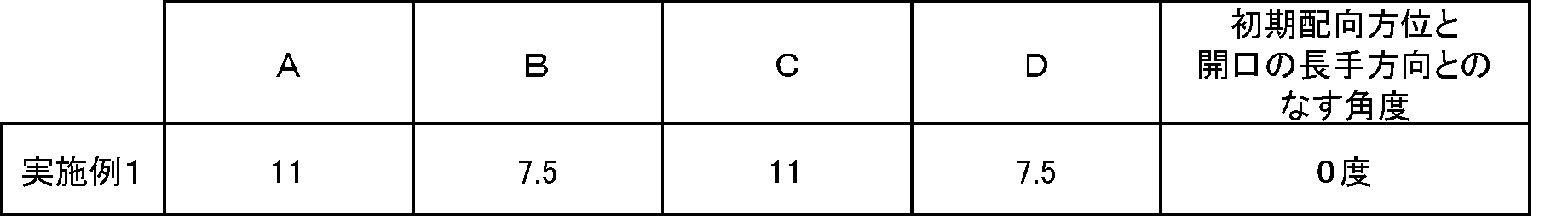
表2より、実施例1で用いた開口15は、A>B、C>Dであり、開口15の長手方向は第三の直線63に平行な方向であった。液晶分子21の初期配向方位22と開口15の長手方向(第三の直線63)とのなす角度は、平面視において0度であり、45度より小さかった。また、実施例1で用いた開口15は、その形状を第一基板10と平行な平面内で180度回転させた際の形状と、面積の100%が重なる形状であった。
From Table 2, the opening 15 used in Example 1 was A> B, C> D, and the longitudinal direction of the opening 15 was a direction parallel to the third straight line 63. The angle formed between the initial alignment direction 22 of the liquid crystal molecules 21 and the longitudinal direction of the opening 15 (third straight line 63) was 0 degrees in plan view and smaller than 45 degrees. In addition, the opening 15 used in Example 1 had a shape that overlaps 100% of the area when the shape was rotated 180 degrees in a plane parallel to the first substrate 10.
[比較例1]
図20は、比較例1の液晶表示装置の平面模式図である。比較例1の液晶表示装置100Aは、対向電極14の開口15の形状を図20の形状に変更したこと以外は、実施例1の液晶表示装置100Aと同様の構成を有する。 [Comparative Example 1]
FIG. 20 is a schematic plan view of the liquid crystal display device of Comparative Example 1. The liquidcrystal display device 100A of Comparative Example 1 has the same configuration as the liquid crystal display device 100A of Example 1 except that the shape of the opening 15 of the counter electrode 14 is changed to the shape of FIG.
図20は、比較例1の液晶表示装置の平面模式図である。比較例1の液晶表示装置100Aは、対向電極14の開口15の形状を図20の形状に変更したこと以外は、実施例1の液晶表示装置100Aと同様の構成を有する。 [Comparative Example 1]
FIG. 20 is a schematic plan view of the liquid crystal display device of Comparative Example 1. The liquid
比較例1で用いた開口15の輪郭の傾きの平均を、実施例1と同様にして求めた。
下記表3に、比較例1で用いた開口15の輪郭部分の傾きの平均及び輪郭全体の傾きの平均を示す。 The average inclination of the contour of theopening 15 used in Comparative Example 1 was determined in the same manner as in Example 1.
Table 3 below shows the average inclination of the contour portion of theopening 15 used in Comparative Example 1 and the average inclination of the entire contour.
下記表3に、比較例1で用いた開口15の輪郭部分の傾きの平均及び輪郭全体の傾きの平均を示す。 The average inclination of the contour of the
Table 3 below shows the average inclination of the contour portion of the

表3より、第一象限71及び第三象限73上の第一及び第三輪郭部分の傾きの平均は負、第二象限72及び第四象限74上の第二及び第四輪郭部分の傾きの平均は正であり、各輪郭部分の傾きの平均の符号は、隣接する2つの輪郭部分の各々の傾きの平均の符号と異なっていた。また、輪郭全体の傾きの平均はゼロであった。
From Table 3, the average of the slopes of the first and third contour portions on the first quadrant 71 and the third quadrant 73 is negative, and the slopes of the second and fourth contour portions on the second quadrant 72 and the fourth quadrant 74 are negative. The average was positive, and the average sign of the slope of each contour portion was different from the average sign of the slope of each of the two adjacent contour portions. Moreover, the average of the inclination of the whole outline was zero.
[実施例1及び比較例1の対比]
図10及び図21に基づき、実施例1及び比較例1の液晶表示装置100Aのオン状態における液晶分子21の配向分布について説明する。
図10は、実施例1の液晶表示装置100Aに関する図であり、(1)は対向電極及び画素電極を示した平面模式図であり、(2)は5.5V印加時の液晶分子の配向分布のシミュレーション結果を示した平面図であり、(3)は6.0V印加時の液晶分子の配向分布のシミュレーション結果を示した平面図である。図21は、比較例1の液晶表示装置に関する図であり、(1)は対向電極及び画素電極を示した平面模式図であり、(2)は4.5V印加時の液晶分子の配向分布のシミュレーション結果を示した平面図であり、(3)は5.0V印加時の液晶分子の配向分布のシミュレーション結果を示した平面図であり、(4)は(3)の点線で囲んだ部分を拡大した平面図である。各実施例及び比較例のシミュレーションには、シンテック社製のLCD-Master3Dを使用した。 [Contrast of Example 1 and Comparative Example 1]
The alignment distribution of theliquid crystal molecules 21 in the ON state of the liquid crystal display device 100A of Example 1 and Comparative Example 1 will be described with reference to FIGS.
FIG. 10 is a diagram relating to the liquidcrystal display device 100A of Example 1, (1) is a schematic plan view showing a counter electrode and a pixel electrode, and (2) is an orientation distribution of liquid crystal molecules when 5.5 V is applied. (3) is a plan view showing the simulation result of the orientation distribution of the liquid crystal molecules when 6.0 V is applied. FIG. 21 is a diagram related to the liquid crystal display device of Comparative Example 1, (1) is a schematic plan view showing a counter electrode and a pixel electrode, and (2) is an orientation distribution of liquid crystal molecules when 4.5 V is applied. It is the top view which showed the simulation result, (3) is the top view which showed the simulation result of the orientation distribution of the liquid crystal molecule at the time of 5.0V application, (4) is the part enclosed with the dotted line of (3). It is the expanded top view. An LCD-Master 3D manufactured by Shintech Co., Ltd. was used for the simulations of the examples and comparative examples.
図10及び図21に基づき、実施例1及び比較例1の液晶表示装置100Aのオン状態における液晶分子21の配向分布について説明する。
図10は、実施例1の液晶表示装置100Aに関する図であり、(1)は対向電極及び画素電極を示した平面模式図であり、(2)は5.5V印加時の液晶分子の配向分布のシミュレーション結果を示した平面図であり、(3)は6.0V印加時の液晶分子の配向分布のシミュレーション結果を示した平面図である。図21は、比較例1の液晶表示装置に関する図であり、(1)は対向電極及び画素電極を示した平面模式図であり、(2)は4.5V印加時の液晶分子の配向分布のシミュレーション結果を示した平面図であり、(3)は5.0V印加時の液晶分子の配向分布のシミュレーション結果を示した平面図であり、(4)は(3)の点線で囲んだ部分を拡大した平面図である。各実施例及び比較例のシミュレーションには、シンテック社製のLCD-Master3Dを使用した。 [Contrast of Example 1 and Comparative Example 1]
The alignment distribution of the
FIG. 10 is a diagram relating to the liquid
図21(2)のシミュレーション結果が示すように、比較例1の液晶表示装置100Aに4.5Vの電圧を印加した場合、1つの開口15あたり4つの液晶ドメインが形成され、4つの表示単位50のいずれにおいても同様の配向状態を示した。しかしながら、比較例1の液晶表示装置100Aに5.0Vの電圧を印加すると、図21(3)の点線で囲んだ部分及び図21(4)に示すように、開口中央部の液晶分子21の配向状態が不安定になり、一部の開口15において液晶分子21が中央部分で回転してしまっている。これは、同じ階調を表示しているにもかかわらず、表示単位50によって配向が異なるために透過率が異なることを意味している。したがって、比較例1の液晶表示装置100Aは、4.5Vまでは使用することができるが、5.0V以上では使用することができないことが分かった。
As shown in the simulation result of FIG. 21 (2), when a voltage of 4.5 V is applied to the liquid crystal display device 100A of Comparative Example 1, four liquid crystal domains are formed per one opening 15, and four display units 50 are formed. In both cases, the same orientation state was shown. However, when a voltage of 5.0 V is applied to the liquid crystal display device 100A of Comparative Example 1, the portion surrounded by the dotted line in FIG. 21 (3) and the liquid crystal molecules 21 at the center of the opening as shown in FIG. 21 (4). The alignment state becomes unstable, and the liquid crystal molecules 21 are rotated at the central portion in some openings 15. This means that although the same gradation is displayed, the transmittance differs because the orientation differs depending on the display unit 50. Therefore, it was found that the liquid crystal display device 100A of Comparative Example 1 can be used up to 4.5V, but cannot be used at 5.0V or higher.
一方、図10(2)及び(3)のシミュレーション結果が示すように、実施例1の液晶表示装置100Aでは、上述の(条件1)及び(条件2)を満たす開口15を用いることにより、電圧印加時に、開口部60内において、1つの開口15あたり4つの液晶ドメインを形成しつつ、開口15の中央部において液晶分子21を決まった方位に回転させ、4つの液晶ドメインのうちの2つを開口15の中央部で繋げることが可能となった。
On the other hand, as shown in the simulation results of FIGS. 10 (2) and 10 (3), in the liquid crystal display device 100A according to the first embodiment, by using the opening 15 that satisfies the above (Condition 1) and (Condition 2), the voltage is increased. At the time of application, while forming four liquid crystal domains per opening 15 in the opening 60, the liquid crystal molecules 21 are rotated in a fixed orientation at the center of the opening 15, and two of the four liquid crystal domains are moved. It became possible to connect at the center of the opening 15.
これにより、5.5V、6.0Vと高電圧を印加しても液晶分子21は全ての表示単位50で同じ配向状態をとることが可能となり、実施例1の液晶表示装置100Aでは表示単位50によって透過率が異なるという課題は発生しなかった。したがって、実施例1の液晶表示装置100Aでは高電圧を印加することができ、透過率を高めることが可能となった。具体的には、白表示の際、実施例1の液晶表示装置100Aに6.0Vの電圧を印加すると、透過率は23.8%となった。これに対して、白表示の際、比較例1の液晶表示装置100Aに4.5Vの電圧を印加すると、透過率は21.2%となった。以上より、実施例1の液晶表示装置100Aでは、比較例1の液晶表示装置100Aと比較して、透過率を12.3%高めることができた。
As a result, even when a high voltage of 5.5 V or 6.0 V is applied, the liquid crystal molecules 21 can have the same alignment state in all the display units 50. In the liquid crystal display device 100A of Example 1, the display unit 50 There was no problem that the transmittance was different. Therefore, in the liquid crystal display device 100A of Example 1, a high voltage can be applied and the transmittance can be increased. Specifically, when a voltage of 6.0 V was applied to the liquid crystal display device 100A of Example 1 during white display, the transmittance was 23.8%. On the other hand, when white voltage was displayed, when a voltage of 4.5 V was applied to the liquid crystal display device 100A of Comparative Example 1, the transmittance was 21.2%. From the above, the liquid crystal display device 100A of Example 1 was able to increase the transmittance by 12.3% as compared with the liquid crystal display device 100A of Comparative Example 1.
実施例1及び比較例1の液晶表示装置100Aの透過率の違いについて以下に考察する。
図11は、実施例1に関する図であり、(1)は対向電極における1つの開口及び画素電極を示した平面図であり、(2)は(1)を第一基板と平行な平面内で180度回転させた図であり、(3)は(1)の開口における電圧印加時の電界分布を示した図であり、(4)は(1)の開口における電圧印加時の透過率分布を示した図である。 The difference in transmittance between the liquidcrystal display device 100A of Example 1 and Comparative Example 1 will be considered below.
FIG. 11 is a diagram related to Example 1, (1) is a plan view showing one opening and pixel electrode in the counter electrode, and (2) is (1) in a plane parallel to the first substrate. It is the figure rotated 180 degree | times, (3) is the figure which showed the electric field distribution at the time of the voltage application in the opening of (1), (4) is the transmittance | permeability distribution at the time of the voltage application in the opening of (1). FIG.
図11は、実施例1に関する図であり、(1)は対向電極における1つの開口及び画素電極を示した平面図であり、(2)は(1)を第一基板と平行な平面内で180度回転させた図であり、(3)は(1)の開口における電圧印加時の電界分布を示した図であり、(4)は(1)の開口における電圧印加時の透過率分布を示した図である。 The difference in transmittance between the liquid
FIG. 11 is a diagram related to Example 1, (1) is a plan view showing one opening and pixel electrode in the counter electrode, and (2) is (1) in a plane parallel to the first substrate. It is the figure rotated 180 degree | times, (3) is the figure which showed the electric field distribution at the time of the voltage application in the opening of (1), (4) is the transmittance | permeability distribution at the time of the voltage application in the opening of (1). FIG.
図11(1)及び(2)に示すように、実施例1で用いた開口15の形状は、液晶分子21の初期配向方位22に対して非対称であり、かつ、その形状を第一基板10と平行な平面内で180度回転させた際の形状と同じである。
As shown in FIGS. 11A and 11B, the shape of the opening 15 used in Example 1 is asymmetric with respect to the initial orientation direction 22 of the liquid crystal molecules 21, and the shape is the first substrate 10. The shape is the same as when rotated 180 degrees in a plane parallel to the.
図11(3)及び(4)に示すように、実施例1のような開口15を用いることで、電圧印加時に4方位にフリンジ電界が発生し、(a)~(d)で示される液晶分子21のように液晶分子21が回転した。また、左上及び右下方向のフリンジ電界は右上及び左下のフリンジ電界より強いことから、中央部の液晶分子21は、強いフリンジ電界の方向に回転した。これにより、開口15の中央部において、液晶分子21を決まった方位へ回転させ、液晶表示装置100Aの応答速度及び透過率を向上させることが可能となった。そして、上述のように、開口15の形状が、液晶分子21の初期配向方位22に対して非対称であり、かつ、その形状を第一基板10と平行な平面内で180度回転させた際の形状と同じである場合に、このような電界を効率よく発生することができる。後述する他の全ての実施例における開口の形状もこの条件を満たす。
As shown in FIGS. 11 (3) and 11 (4), by using the opening 15 as in the first embodiment, a fringe electric field is generated in four directions when a voltage is applied, and the liquid crystal shown in (a) to (d). Like the molecule 21, the liquid crystal molecule 21 was rotated. In addition, since the fringe electric fields in the upper left and lower right directions are stronger than the upper right and lower left fringe electric fields, the liquid crystal molecules 21 in the central portion rotate in the direction of the strong fringe electric fields. This makes it possible to rotate the liquid crystal molecules 21 in a fixed direction at the center of the opening 15 and improve the response speed and transmittance of the liquid crystal display device 100A. As described above, the shape of the opening 15 is asymmetric with respect to the initial orientation direction 22 of the liquid crystal molecules 21 and the shape is rotated 180 degrees in a plane parallel to the first substrate 10. When the shape is the same, such an electric field can be generated efficiently. The shape of the opening in all other embodiments described later also satisfies this condition.
図22は比較例1に関する図であり、(1)は対向電極における1つの開口及び画素電極を示した平面図であり、(2)は(1)の開口における電圧印加時の電界分布1を示した図であり、(3)は(2)の状態での透過率分布1を示した図であり、(4)は(1)の開口における電圧印加時の電界分布2を示した図であり、(5)は(4)の状態での透過率分布2を示した図である。
22 is a diagram related to Comparative Example 1, (1) is a plan view showing one opening and a pixel electrode in the counter electrode, and (2) is an electric field distribution 1 when voltage is applied to the opening in (1). (3) is a diagram showing a transmittance distribution 1 in the state of (2), and (4) is a diagram showing an electric field distribution 2 when a voltage is applied to the opening of (1). And (5) is a diagram showing the transmittance distribution 2 in the state of (4).
比較例1の対向電極14を用いた場合、理想的には開口15の長手方向及び短手方向に対して対称な4つの領域内に4つの液晶ドメインが発生し、開口15の中央部では電界のバランスがとれて液晶分子21は回転しない。しかしながら実際は、高電圧になると、開口15の中央部の電界が若干歪み、図22(2)及び(3)のように液晶分子21が左に回転してしまったり、図22(4)及び(5)のように電界のバランスがとれて液晶分子21が回転しなかったりする。このように、比較例1では、高電圧を印加した際の液晶分子21の配向状態が表示単位50によって異なるため、高電圧を印加することができず、結果として液晶表示装置100Aの透過率の低下を招いてしまう。
When the counter electrode 14 of Comparative Example 1 is used, ideally, four liquid crystal domains are generated in four regions symmetrical with respect to the longitudinal direction and the short direction of the opening 15, and an electric field is generated at the center of the opening 15. And the liquid crystal molecules 21 do not rotate. However, in reality, when the voltage becomes high, the electric field at the center of the opening 15 is slightly distorted, and the liquid crystal molecules 21 are rotated to the left as shown in FIGS. 22 (2) and (3). As in 5), the electric field is balanced and the liquid crystal molecules 21 do not rotate. Thus, in Comparative Example 1, since the alignment state of the liquid crystal molecules 21 when a high voltage is applied differs depending on the display unit 50, a high voltage cannot be applied, and as a result, the transmittance of the liquid crystal display device 100A is reduced. It will cause a decline.
[実施例2~4]
図12~図14は、それぞれ、実施例2~4の液晶表示装置に関する図であり、(1)は液晶表示装置の平面模式図であり、(2)は対向電極及び画素電極を示した平面模式図であり、(3)は6.0V印加時の液晶分子の配向分布のシミュレーション結果を示した平面図である。
実施例2~4の液晶表示装置100Aは、対向電極14における開口15の形状を変更したこと以外は、実施例1の液晶表示装置100Aと同様の構成を有する。実施例2~4の液晶表示装置100Aではそれぞれ、図12~図14に示す開口15が設けられた対向電極14を用いた。図12~図14にはそれぞれ、実施例2~4における液晶分子21の初期配向方位22を示す。また、図3(2)~(4)は、実施例2~4で用いた開口15の形状とA及びBとの関係を示しており、図5(2)~(4)は、実施例2~4で用いた開口15の形状とC及びDとの関係を示している。 [Examples 2 to 4]
FIGS. 12 to 14 are diagrams relating to the liquid crystal display devices of Examples 2 to 4, respectively. (1) is a schematic plan view of the liquid crystal display device, and (2) is a plan view showing a counter electrode and a pixel electrode. It is a schematic diagram, (3) is a plan view showing a simulation result of the orientation distribution of liquid crystal molecules when 6.0 V is applied.
The liquidcrystal display device 100A of the second to fourth embodiments has the same configuration as the liquid crystal display device 100A of the first embodiment, except that the shape of the opening 15 in the counter electrode 14 is changed. In the liquid crystal display devices 100A of Examples 2 to 4, the counter electrode 14 provided with the opening 15 shown in FIGS. 12 to 14 was used. FIG. 12 to FIG. 14 show initial alignment directions 22 of the liquid crystal molecules 21 in Examples 2 to 4, respectively. 3 (2) to (4) show the relationship between the shape of the opening 15 used in Examples 2 to 4 and A and B, and FIGS. 5 (2) to (4) show the examples. The relationship between the shape of the opening 15 used in 2 to 4 and C and D is shown.
図12~図14は、それぞれ、実施例2~4の液晶表示装置に関する図であり、(1)は液晶表示装置の平面模式図であり、(2)は対向電極及び画素電極を示した平面模式図であり、(3)は6.0V印加時の液晶分子の配向分布のシミュレーション結果を示した平面図である。
実施例2~4の液晶表示装置100Aは、対向電極14における開口15の形状を変更したこと以外は、実施例1の液晶表示装置100Aと同様の構成を有する。実施例2~4の液晶表示装置100Aではそれぞれ、図12~図14に示す開口15が設けられた対向電極14を用いた。図12~図14にはそれぞれ、実施例2~4における液晶分子21の初期配向方位22を示す。また、図3(2)~(4)は、実施例2~4で用いた開口15の形状とA及びBとの関係を示しており、図5(2)~(4)は、実施例2~4で用いた開口15の形状とC及びDとの関係を示している。 [Examples 2 to 4]
FIGS. 12 to 14 are diagrams relating to the liquid crystal display devices of Examples 2 to 4, respectively. (1) is a schematic plan view of the liquid crystal display device, and (2) is a plan view showing a counter electrode and a pixel electrode. It is a schematic diagram, (3) is a plan view showing a simulation result of the orientation distribution of liquid crystal molecules when 6.0 V is applied.
The liquid
実施例2及び実施例3で用いた開口15の輪郭部分及び輪郭全体の傾きの平均は、実施例1と同様に求めた。実施例4で用いた開口15の輪郭部分及び輪郭全体の傾きの平均は、x軸に投影した各々の輪郭部分の長さを210等分する、y軸に平行な211本の直線を引いたこと以外、実施例1と同様にして求めた。なお、実施例3で用いた開口15のように、輪郭部分が第一の直線61又は第二の直線62に平行な部分を含む場合は、その平行な部分を除外して輪郭部分の傾きの平均を求めるものとする。下記表4に、実施例2~4で用いた開口15の輪郭部分の傾きの平均及び輪郭全体の傾きの平均を示す。
The average of the inclination of the contour portion of the opening 15 and the entire contour used in Example 2 and Example 3 was obtained in the same manner as in Example 1. The average of the inclination of the contour portion of the opening 15 and the entire contour used in Example 4 was obtained by subtracting 211 straight lines parallel to the y axis that divide the length of each contour portion projected onto the x axis into 210 equal parts. Except for this, it was determined in the same manner as in Example 1. In addition, when the contour portion includes a portion parallel to the first straight line 61 or the second straight line 62 like the opening 15 used in the third embodiment, the inclination of the contour portion is excluded by excluding the parallel portion. The average shall be obtained. Table 4 below shows the average inclination of the contour portion of the opening 15 and the average inclination of the entire contour used in Examples 2 to 4.
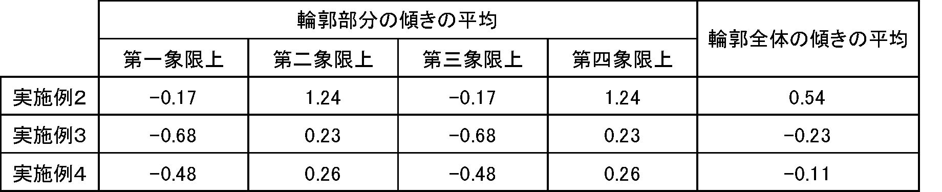
表4より、第一象限71及び第三象限73上の第一及び第三輪郭部分の傾きの平均は負、第二象限72及び第四象限74上の第二及び第四輪郭部分の傾きの平均は正であり、各輪郭部分の傾きの平均の符号は、隣接する2つの輪郭部分の各々の傾きの平均の符号と異なっていた。また、輪郭全体の傾きの平均はゼロではなかった。
From Table 4, the average of the slopes of the first and third contour portions on the first quadrant 71 and the third quadrant 73 is negative, and the slopes of the second and fourth contour portions on the second quadrant 72 and the fourth quadrant 74 are negative. The average was positive, and the average sign of the slope of each contour portion was different from the average sign of the slope of each of the two adjacent contour portions. Moreover, the average of the inclination of the whole outline was not zero.
A~Dの長さ及び液晶分子21の初期配向方位22と開口15の長手方向とのなす角度を下記表5に示す。
Table 5 below shows the lengths A to D and the angle between the initial orientation direction 22 of the liquid crystal molecules 21 and the longitudinal direction of the openings 15.
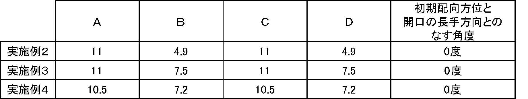
表5より、実施例2~4で用いた開口15は、A>B、C>Dであり、開口15の長手方向は第三の直線63に平行な方向であった。初期配向方位22と開口15の長手方向とのなす角度は、平面視において0度であり、45度より小さかった。また、実施例2~4で用いた開口15は、その形状を第一基板10と平行な平面内で180度回転させた際の形状と、面積の100%が重なる形状であった。
From Table 5, the openings 15 used in Examples 2 to 4 were A> B and C> D, and the longitudinal direction of the openings 15 was parallel to the third straight line 63. The angle formed between the initial orientation azimuth 22 and the longitudinal direction of the opening 15 was 0 degrees in plan view and smaller than 45 degrees. In addition, the opening 15 used in Examples 2 to 4 had a shape that overlaps 100% of the area when the shape was rotated 180 degrees in a plane parallel to the first substrate 10.
図12~図14に基づき、実施例2~4の液晶表示装置100Aのオン状態における液晶分子21の配向分布について説明する。
The alignment distribution of the liquid crystal molecules 21 in the on state of the liquid crystal display devices 100A of Examples 2 to 4 will be described with reference to FIGS.
図12(3)~図14(3)のシミュレーション結果が示すように、実施例2~4の液晶表示装置100Aでは、上述の(条件1)及び(条件2)を満たす開口15を用いることにより、電圧印加時に、開口部60内において、1つの開口15あたり4つの液晶ドメインを形成しつつ、開口15の中央部において液晶分子21を決まった方位に回転させ、4つの液晶ドメインのうちの2つを開口15の中央部で繋げることが可能となった。
As shown in the simulation results of FIGS. 12 (3) to 14 (3), in the liquid crystal display devices 100A of Examples 2 to 4, the openings 15 satisfying the above (Condition 1) and (Condition 2) are used. When a voltage is applied, four liquid crystal domains are formed per one opening 15 in the opening 60, and the liquid crystal molecules 21 are rotated in a predetermined direction in the center of the opening 15 to rotate out of two of the four liquid crystal domains. It became possible to connect the two at the center of the opening 15.
これにより、実施例2~4の液晶表示装置100Aでは6.0Vの高電圧を印加しても液晶分子21は全ての表示単位50で同じ配向状態をとることが可能となり、透過率を高めることが可能となった。具体的には、白表示の際に6.0Vの電圧を印加すると、実施例2~4の液晶表示装置100Aにおける透過率はそれぞれ、24.7%、24.2%及び23.6%となった。前述の比較例1の液晶表示装置100Aと比較して、実施例2~4の液晶表示装置100Aはそれぞれ、透過率を16%、14%及び11%高めることができた。
As a result, in the liquid crystal display devices 100A of Examples 2 to 4, even when a high voltage of 6.0 V is applied, the liquid crystal molecules 21 can have the same alignment state in all the display units 50, and the transmittance is increased. Became possible. Specifically, when a voltage of 6.0 V is applied during white display, the transmittances in the liquid crystal display devices 100A of Examples 2 to 4 are 24.7%, 24.2%, and 23.6%, respectively. became. Compared with the liquid crystal display device 100A of Comparative Example 1 described above, the liquid crystal display devices 100A of Examples 2 to 4 were able to increase the transmittance by 16%, 14%, and 11%, respectively.
[実施例5]
実施例5の液晶表示装置100Aは、対向電極14における開口15の形状、液晶分子21の初期配向方位22及び一対の偏光子の偏光軸を変更したこと以外は、実施例1の液晶表示装置100Aと同様の構成を有する。図15は、実施例5の液晶表示装置の平面模式図である。実施例5で用いた対向電極14の形状は比較例1と同様にしたが、実施例5の液晶分子21の初期配向方位22及び一対の偏光子の偏光軸は比較例1の角度から10度傾けた。図15には、液晶分子21の初期配向方位22を示す。また、図3(5)は、実施例5で用いた開口15の形状とA及びBとの関係を示しており、図5(5)は、実施例5で用いた開口15の形状とC及びDとの関係を示している。 [Example 5]
The liquidcrystal display device 100A of the fifth embodiment is the same as the liquid crystal display device 100A of the first embodiment except that the shape of the opening 15 in the counter electrode 14, the initial orientation direction 22 of the liquid crystal molecules 21 and the polarization axes of the pair of polarizers are changed. It has the same configuration as. FIG. 15 is a schematic plan view of the liquid crystal display device according to the fifth embodiment. The shape of the counter electrode 14 used in Example 5 was the same as that of Comparative Example 1, but the initial orientation direction 22 of the liquid crystal molecules 21 of Example 5 and the polarization axis of the pair of polarizers were 10 degrees from the angle of Comparative Example 1. Tilt. FIG. 15 shows the initial alignment direction 22 of the liquid crystal molecules 21. FIG. 3 (5) shows the relationship between the shape of the opening 15 used in Example 5 and A and B, and FIG. 5 (5) shows the shape of the opening 15 used in Example 5 and C. And the relationship with D.
実施例5の液晶表示装置100Aは、対向電極14における開口15の形状、液晶分子21の初期配向方位22及び一対の偏光子の偏光軸を変更したこと以外は、実施例1の液晶表示装置100Aと同様の構成を有する。図15は、実施例5の液晶表示装置の平面模式図である。実施例5で用いた対向電極14の形状は比較例1と同様にしたが、実施例5の液晶分子21の初期配向方位22及び一対の偏光子の偏光軸は比較例1の角度から10度傾けた。図15には、液晶分子21の初期配向方位22を示す。また、図3(5)は、実施例5で用いた開口15の形状とA及びBとの関係を示しており、図5(5)は、実施例5で用いた開口15の形状とC及びDとの関係を示している。 [Example 5]
The liquid
実施例5で用いた開口15の輪郭部分及び輪郭全体の傾きの平均は、x軸に投影した各々の輪郭部分の長さを210等分する、y軸に平行な211本の直線を引いたこと以外、実施例1と同様にして求めた。下記表6に、実施例5で用いた開口15の輪郭部分の傾きの平均及び輪郭全体の傾きの平均を示す。
The average of the inclination of the contour portion of the opening 15 and the whole contour used in Example 5 was obtained by subtracting 211 straight lines parallel to the y-axis that divide the length of each contour portion projected onto the x-axis into 210 equal parts. Except for this, it was determined in the same manner as in Example 1. Table 6 below shows the average inclination of the contour portion of the opening 15 used in Example 5 and the average inclination of the entire contour.
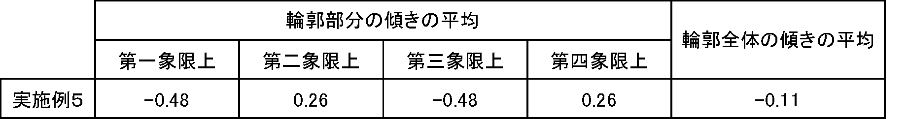
表6より、第一象限71及び第三象限73上の第一及び第三輪郭部分の傾きの平均は負、第二象限72及び第四象限74上の第二及び第四輪郭部分の傾きの平均は正であり、各輪郭部分の傾きの平均の符号は、隣接する2つの輪郭部分の各々の傾きの平均の符号と異なっていた。また、輪郭全体の傾きの平均はゼロではなかった。
From Table 6, the average of the slopes of the first and third contour portions on the first quadrant 71 and the third quadrant 73 is negative, and the slopes of the second and fourth contour portions on the second quadrant 72 and the fourth quadrant 74 are negative. The average was positive, and the average sign of the slope of each contour portion was different from the average sign of the slope of each of the two adjacent contour portions. Moreover, the average of the inclination of the whole outline was not zero.
A~Dの長さ及び液晶分子21の初期配向方位22と開口15の長手方向とのなす角度を下記表7に示す。
Table 7 below shows the lengths A to D and the angle between the initial orientation direction 22 of the liquid crystal molecules 21 and the longitudinal direction of the openings 15.
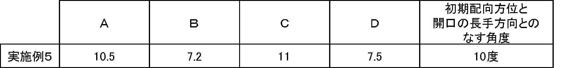
表7より、実施例5で用いた開口15は、A>B、C>Dであり、開口15の長手方向は第三の直線63に平行な方向であった。初期配向方位22と開口15の長手方向とのなす角度は、平面視において10度であり、45度より小さかった。また、実施例1で用いた開口15は、その形状を第一基板10と平行な平面内で180度回転させた際の形状と、面積の100%が重なる形状であった。
From Table 7, the opening 15 used in Example 5 was A> B, C> D, and the longitudinal direction of the opening 15 was a direction parallel to the third straight line 63. The angle formed by the initial orientation direction 22 and the longitudinal direction of the opening 15 was 10 degrees in plan view, and was smaller than 45 degrees. In addition, the opening 15 used in Example 1 had a shape that overlaps 100% of the area when the shape was rotated 180 degrees in a plane parallel to the first substrate 10.
図16に基づき、実施例5の液晶表示装置100Aのオン状態における液晶分子21の配向分布について説明する。図16は、実施例5の液晶表示装置に関する図であり、(1)は対向電極及び画素電極を示した平面模式図であり、(2)は5.5V印加時の液晶分子の配向分布のシミュレーション結果を示した平面図であり、(3)は6.0V印加時の液晶分子の配向分布のシミュレーション結果を示した平面図である。図16(2)及び(3)のシミュレーション結果が示すように、実施例5の液晶表示装置100Aでは、上述の(条件1)及び(条件2)を満たす開口15を用いることにより、電圧印加時に、1つの開口15あたり4つの液晶ドメインを形成しつつ、開口15の中央部において液晶分子21を決まった方位に回転させ、4つの液晶ドメインのうちの2つを開口15の中央部で繋げることが可能となった。
Based on FIG. 16, the orientation distribution of the liquid crystal molecules 21 in the ON state of the liquid crystal display device 100A of Example 5 will be described. FIG. 16 is a diagram relating to the liquid crystal display device of Example 5, (1) is a schematic plan view showing a counter electrode and a pixel electrode, and (2) is an orientation distribution of liquid crystal molecules when 5.5 V is applied. It is the top view which showed the simulation result, (3) is the top view which showed the simulation result of the orientation distribution of the liquid crystal molecule at the time of 6.0V application. As shown in the simulation results of FIGS. 16 (2) and 16 (3), in the liquid crystal display device 100A of Example 5, the opening 15 satisfying the above (Condition 1) and (Condition 2) is used, so that a voltage is applied. While forming four liquid crystal domains per opening 15, the liquid crystal molecules 21 are rotated in a predetermined orientation at the center of the opening 15, and two of the four liquid crystal domains are connected at the center of the opening 15. Became possible.
これにより、5.5V、6.0Vと高電圧を印加しても液晶分子21は全ての表示単位50で同じ配向状態をとることが可能となり、実施例5の液晶表示装置100Aでは表示単位50によって透過率が異なるという課題は発生しなかった。したがって、実施例5の液晶表示装置100Aでは高電圧を印加することができ、透過率を高めることが可能となった。具体的には、白表示の際、実施例5の液晶表示装置100Aに6.0Vの電圧を印加すると、透過率は23.9%となった。これに対して、白表示の際、比較例1の液晶表示装置100Aに4.5Vの電圧を印加すると、透過率は21.2%となった。以上より、実施例5の液晶表示装置100Aでは、比較例1の液晶表示装置100Aと比較して、透過率を12.7%高めることができた。
As a result, even when a high voltage of 5.5 V or 6.0 V is applied, the liquid crystal molecules 21 can have the same alignment state in all the display units 50. In the liquid crystal display device 100A of Example 5, the display unit 50 There was no problem that the transmittance was different. Therefore, in the liquid crystal display device 100A of Example 5, a high voltage can be applied and the transmittance can be increased. Specifically, when a voltage of 6.0 V was applied to the liquid crystal display device 100A of Example 5 during white display, the transmittance was 23.9%. On the other hand, when white voltage was displayed, when a voltage of 4.5 V was applied to the liquid crystal display device 100A of Comparative Example 1, the transmittance was 21.2%. From the above, the liquid crystal display device 100A of Example 5 was able to increase the transmittance by 12.7% compared to the liquid crystal display device 100A of Comparative Example 1.
[付記]
本発明の一態様は、第一基板と、液晶分子を含有する液晶層と、第二基板とを順に備え、上記第一基板は、第一電極と、上記第一電極よりも上記液晶層側に設けられた第二電極と、上記第一電極と上記第二電極との間に設けられた絶縁膜とを有し、上記第二電極には開口が形成され、上記第一電極と上記第二電極の間に電圧が印加されない電圧無印加状態において、上記液晶分子は、上記第一基板に対して平行に配向し、上記液晶分子の初期配向方位に対して平行であり、かつ、上記開口を分断する長さが最長となる第一の直線と、上記初期配向方位に対して直交し、かつ、上記開口を分断する長さが最長となる第二の直線とで上記開口の輪郭を4つに分断すると、分断された各輪郭部分の傾きの平均の符号は、隣接する2つの輪郭部分の各々の傾きの平均の符号と異なり、上記開口の上記輪郭全体の傾きの平均は、ゼロではない液晶表示装置であってもよい。 [Appendix]
One embodiment of the present invention includes a first substrate, a liquid crystal layer containing liquid crystal molecules, and a second substrate in order, and the first substrate is closer to the liquid crystal layer than the first electrode and the first electrode. A second electrode provided on the first electrode and an insulating film provided between the first electrode and the second electrode, wherein the second electrode has an opening, and the first electrode and the first electrode In a state where no voltage is applied between the two electrodes, the liquid crystal molecules are aligned parallel to the first substrate, parallel to the initial alignment direction of the liquid crystal molecules, and the opening. The outline of the opening is defined by a first straight line having the longest length to divide the opening and a second straight line orthogonal to the initial orientation direction and having the longest length to divide the opening. When divided into two, the average sign of the slope of each divided contour portion is calculated for each of the two adjacent contour portions. Unlike the average of the sign of the slope, the average of the outline overall inclination of the opening may be a liquid crystal display device not zero.
各輪郭部分の傾きの平均の符号が、隣接する2つの輪郭部分の各々の傾きの平均の符号と異なることにより、隣接する輪郭部分において、液晶分子21を逆方位に回転させる電界を発生させることが可能となる。また、開口の輪郭全体の傾きの平均はゼロではないため、開口の形状は液晶分子の初期配向方位に対して非対称となり、開口の中央部における液晶分子の回転を1方位に決定することができる。これにより、高電圧印加時に表示単位によって液晶分子の配向状態が異なるという現象の発生を低減でき、全ての表示単位で高電圧印加時にも液晶分子の配向が安定する。そのため、充分に高い電圧を印加でき、透過率を向上させることが可能となる。
The average sign of the inclination of each contour portion is different from the average sign of each of the two adjacent contour portions, thereby generating an electric field that rotates the liquid crystal molecules 21 in the opposite direction in the adjacent contour portions. Is possible. In addition, since the average inclination of the entire contour of the opening is not zero, the shape of the opening is asymmetric with respect to the initial alignment direction of the liquid crystal molecules, and the rotation of the liquid crystal molecules at the center of the opening can be determined as one direction. . As a result, the occurrence of the phenomenon that the alignment state of the liquid crystal molecules differs depending on the display unit when a high voltage is applied can be reduced, and the alignment of the liquid crystal molecules is stabilized even when a high voltage is applied in all display units. Therefore, a sufficiently high voltage can be applied and the transmittance can be improved.
また、上述のような条件を満たす開口は、特に複雑な形状を取らなくても形成可能であるため、高精細化を実現することができる。
In addition, an opening that satisfies the above conditions can be formed without taking a particularly complicated shape, so that high definition can be realized.
上記第一の直線及び上記第二の直線のうち、上記開口を分断する長さが長い方をx軸とし、かつ、上記第一の直線及び上記第二の直線のうち、上記開口を分断する長さが短い方をy軸としたとき、又は、上記第一の直線及び上記第二の直線の上記開口を分断する長さが互いに等しい場合は、上記第一の直線及び上記第二の直線のいずれか一方をx軸とし、他方をy軸としたとき、第一象限及び第三象限上の輪郭部分の各々の傾きの平均は、負であり、第二象限及び第四象限上の輪郭部分の各々の傾きの平均は、正であってもよい。この態様によれば、開口の形状を更に簡便なものとすることができるため、更なる高精細化が可能となる。
Of the first straight line and the second straight line, the longer one that divides the opening is the x-axis, and the opening is divided among the first straight line and the second straight line. When the shorter length is the y-axis, or when the lengths of the first straight line and the second straight line dividing the opening are equal to each other, the first straight line and the second straight line When one of the x axis is the y axis and the other is the y axis, the average of the slopes of the contour portions in the first quadrant and the third quadrant is negative, and the contour in the second quadrant and the fourth quadrant The average of the slopes of each of the portions may be positive. According to this aspect, since the shape of the opening can be further simplified, further high definition can be achieved.
上記液晶分子は、正の誘電率異方性を有していてもよい。この態様によれば、相対的に粘度の低い液晶分子を用いることができ、応答速度をより向上させることができる。
The liquid crystal molecules may have a positive dielectric anisotropy. According to this aspect, liquid crystal molecules having a relatively low viscosity can be used, and the response speed can be further improved.
上記第一の直線上における開口の長さをAとし、上記第二の直線上における開口の長さをBとしたとき、A>Bであってもよい。この態様によれば、透過率及び配向安定性をより向上させることができる。
When the length of the opening on the first straight line is A and the length of the opening on the second straight line is B, A> B may be satisfied. According to this aspect, the transmittance and the alignment stability can be further improved.
上記初期配向方位と、上記開口の長手方向とのなす角度は、平面視において、45度以下であってもよい。この態様によれば、透過率及び配向安定性をより向上させることができる。
The angle formed by the initial orientation direction and the longitudinal direction of the opening may be 45 degrees or less in plan view. According to this aspect, the transmittance and the alignment stability can be further improved.
上記液晶分子は、負の誘電率異方性を有していてもよい。
The liquid crystal molecules may have negative dielectric anisotropy.
上記第一の直線上における開口の長さをAとし、上記第二の直線上における開口の長さをBとしたとき、A<Bであってもよい。この態様によれば、透過率及び配向安定性をより向上させることができる。
When the length of the opening on the first straight line is A and the length of the opening on the second straight line is B, A <B may be satisfied. According to this aspect, the transmittance and the alignment stability can be further improved.
上記初期配向方位と、上記開口の長手方向とのなす角度は、平面視において、45度以上であってもよい。この態様によれば、透過率及び配向安定性をより向上させることができる。
The angle formed by the initial orientation direction and the longitudinal direction of the opening may be 45 degrees or more in plan view. According to this aspect, the transmittance and the alignment stability can be further improved.
上記第一電極と上記第二電極の間に電圧が印加された電圧印加状態において、上記液晶分子は、上記開口の中央部において、同一の方位に回転してもよい。この態様によれば、高電圧印加時に表示単位によって液晶分子の配向状態が異なるという現象の発生をより確実に低減することができる。
In a voltage application state in which a voltage is applied between the first electrode and the second electrode, the liquid crystal molecules may rotate in the same direction at the center of the opening. According to this aspect, it is possible to more reliably reduce the occurrence of the phenomenon that the alignment state of the liquid crystal molecules differs depending on the display unit when a high voltage is applied.
上記開口の形状は、その形状を上記第一基板と平行な平面内で180度回転させた際の形状と同じであってもよい。この態様によれば、より効率的に所望の配向を実現することができる。
The shape of the opening may be the same as the shape when the shape is rotated 180 degrees in a plane parallel to the first substrate. According to this aspect, the desired orientation can be realized more efficiently.
少なくとも白表示状態において、上記開口上には第一、第二及び第三の液晶ドメインが存在し、上記第一の液晶ドメインは、平面視において、上下左右に隣接する4つの領域のうち、右上及び左下、又は、右下及び左上に位置する2つの領域内にそれぞれ位置する2つのドメイン部分と、上記2つのドメイン部分を連結し、上記開口の中央部に位置する連結部分とを有し、上記第二及び第三の液晶ドメインは、それぞれ、上記2つのドメイン部分が位置しない2つの領域内に位置していてもよい。この態様によれば、高電圧印加時に表示単位によって液晶分子の配向状態が異なるという現象の発生をより確実に低減することができる。
At least in the white display state, the first, second, and third liquid crystal domains exist on the opening, and the first liquid crystal domain is located at the upper right among four regions that are adjacent in the top, bottom, left, and right directions in a plan view. And two domain portions located in the two regions located at the lower left or the lower right and the upper left, respectively, and the two domain portions connected to each other, and a connecting portion located at the center of the opening, The second and third liquid crystal domains may be positioned in two regions where the two domain portions are not positioned. According to this aspect, it is possible to more reliably reduce the occurrence of the phenomenon that the alignment state of the liquid crystal molecules differs depending on the display unit when a high voltage is applied.
10:第一基板
11、31:絶縁基板(例えば、ガラス基板)
12:画素電極(第一電極)
13:絶縁層(絶縁膜)
14:対向電極(第二電極)
15:開口(スリット)
16:長手形状部
17:突出部
20:液晶層
21:液晶分子
22:初期配向方位
30:第二基板
32:カラーフィルタ
33:オーバーコート層
41:ゲート信号線(走査配線)
42:ソース信号線(信号配線)
43:TFT
50:表示単位
60:開口部
61:第一の直線
62:第二の直線
63:第三の直線
64:第四の直線
71:第一象限
72:第二象限
73:第三象限
74:第四象限
81:第一の液晶ドメイン
81A:ドメイン部分
81B:連結部分
82:第二の液晶ドメイン
83:第三の液晶ドメイン
100A:液晶表示装置
A:第一の直線61上における開口15の長さ
B:第二の直線62上における開口15の長さ
C:第三の直線63上における開口15の長さ
D:第四の直線64上における開口15の長さ 10:First substrate 11, 31: Insulating substrate (eg glass substrate)
12: Pixel electrode (first electrode)
13: Insulating layer (insulating film)
14: Counter electrode (second electrode)
15: Opening (slit)
16: Longitudinal shape portion 17: Protruding portion 20: Liquid crystal layer 21: Liquid crystal molecule 22: Initial alignment direction 30: Second substrate 32: Color filter 33: Overcoat layer 41: Gate signal line (scanning wiring)
42: Source signal line (signal wiring)
43: TFT
50: display unit 60: opening 61: first straight line 62: second straight line 63: third straight line 64: fourth straight line 71: first quadrant 72: second quadrant 73: third quadrant 74: first Four quadrants 81: firstliquid crystal domain 81A: domain portion 81B: connecting portion 82: second liquid crystal domain 83: third liquid crystal domain 100A: liquid crystal display device A: length of the opening 15 on the first straight line 61 B: Length of the opening 15 on the second straight line 62 C: Length of the opening 15 on the third straight line 63 D: Length of the opening 15 on the fourth straight line 64
11、31:絶縁基板(例えば、ガラス基板)
12:画素電極(第一電極)
13:絶縁層(絶縁膜)
14:対向電極(第二電極)
15:開口(スリット)
16:長手形状部
17:突出部
20:液晶層
21:液晶分子
22:初期配向方位
30:第二基板
32:カラーフィルタ
33:オーバーコート層
41:ゲート信号線(走査配線)
42:ソース信号線(信号配線)
43:TFT
50:表示単位
60:開口部
61:第一の直線
62:第二の直線
63:第三の直線
64:第四の直線
71:第一象限
72:第二象限
73:第三象限
74:第四象限
81:第一の液晶ドメイン
81A:ドメイン部分
81B:連結部分
82:第二の液晶ドメイン
83:第三の液晶ドメイン
100A:液晶表示装置
A:第一の直線61上における開口15の長さ
B:第二の直線62上における開口15の長さ
C:第三の直線63上における開口15の長さ
D:第四の直線64上における開口15の長さ 10:
12: Pixel electrode (first electrode)
13: Insulating layer (insulating film)
14: Counter electrode (second electrode)
15: Opening (slit)
16: Longitudinal shape portion 17: Protruding portion 20: Liquid crystal layer 21: Liquid crystal molecule 22: Initial alignment direction 30: Second substrate 32: Color filter 33: Overcoat layer 41: Gate signal line (scanning wiring)
42: Source signal line (signal wiring)
43: TFT
50: display unit 60: opening 61: first straight line 62: second straight line 63: third straight line 64: fourth straight line 71: first quadrant 72: second quadrant 73: third quadrant 74: first Four quadrants 81: first
Claims (11)
- 第一基板と、液晶分子を含有する液晶層と、第二基板とを順に備え、
前記第一基板は、第一電極と、前記第一電極よりも前記液晶層側に設けられた第二電極と、前記第一電極と前記第二電極との間に設けられた絶縁膜とを有し、
前記第二電極には開口が形成され、
前記第一電極と前記第二電極の間に電圧が印加されない電圧無印加状態において、前記液晶分子は、前記第一基板に対して平行に配向し、
前記液晶分子の初期配向方位に対して平行であり、かつ、前記開口を分断する長さが最長となる第一の直線と、前記初期配向方位に対して直交し、かつ、前記開口を分断する長さが最長となる第二の直線とで前記開口の輪郭を4つに分断すると、
分断された各輪郭部分の傾きの平均の符号は、隣接する2つの輪郭部分の各々の傾きの平均の符号と異なり、
前記開口の前記輪郭全体の傾きの平均は、ゼロではないことを特徴とする液晶表示装置。 A first substrate, a liquid crystal layer containing liquid crystal molecules, and a second substrate in order,
The first substrate includes a first electrode, a second electrode provided closer to the liquid crystal layer than the first electrode, and an insulating film provided between the first electrode and the second electrode. Have
An opening is formed in the second electrode,
In a voltage non-application state where no voltage is applied between the first electrode and the second electrode, the liquid crystal molecules are aligned in parallel to the first substrate,
The first straight line that is parallel to the initial alignment direction of the liquid crystal molecules and has the longest length to divide the opening is orthogonal to the initial alignment direction and divides the opening. Dividing the outline of the opening into four with the second straight line having the longest length,
The average sign of the slope of each divided contour portion is different from the average sign of the slope of each of the two adjacent contour portions,
The average inclination of the whole outline of the opening is not zero. - 前記第一の直線及び前記第二の直線のうち、前記開口を分断する長さが長い方をx軸とし、かつ、前記第一の直線及び前記第二の直線のうち、前記開口を分断する長さが短い方をy軸としたとき、又は、前記第一の直線及び前記第二の直線の前記開口を分断する長さが互いに等しい場合は、前記第一の直線及び前記第二の直線のいずれか一方をx軸とし、他方をy軸としたとき、第一象限及び第三象限上の輪郭部分の各々の傾きの平均は、負であり、第二象限及び第四象限上の輪郭部分の各々の傾きの平均は、正であることを特徴とする請求項1記載の液晶表示装置。 Of the first straight line and the second straight line, the longer one that divides the opening is the x-axis, and the first straight line and the second straight line are divided. When the shorter length is the y-axis, or when the lengths of the first straight line and the second straight line dividing the opening are equal to each other, the first straight line and the second straight line When one of the x axis is the y axis and the other is the y axis, the average of the slopes of the contour portions in the first quadrant and the third quadrant is negative, and the contour in the second quadrant and the fourth quadrant The liquid crystal display device according to claim 1, wherein an average of inclinations of the respective portions is positive.
- 前記液晶分子は、正の誘電率異方性を有することを特徴とする請求項1又は2記載の液晶表示装置。 The liquid crystal display device according to claim 1, wherein the liquid crystal molecules have positive dielectric anisotropy.
- 前記第一の直線上における開口の長さをAとし、前記第二の直線上における開口の長さをBとしたとき、A>Bであることを特徴とする請求項3記載の液晶表示装置。 4. The liquid crystal display device according to claim 3, wherein A> B, where A is the length of the opening on the first straight line and B is the length of the opening on the second straight line. .
- 前記初期配向方位と、前記開口の長手方向とのなす角度は、平面視において、45度以下であることを特徴とする請求項3又は4記載の液晶表示装置。 5. The liquid crystal display device according to claim 3, wherein an angle formed by the initial orientation direction and a longitudinal direction of the opening is 45 degrees or less in a plan view.
- 前記液晶分子は、負の誘電率異方性を有することを特徴とする請求項1又は2記載の液晶表示装置。 The liquid crystal display device according to claim 1, wherein the liquid crystal molecules have negative dielectric anisotropy.
- 前記第一の直線上における開口の長さをAとし、前記第二の直線上における開口の長さをBとしたとき、A<Bであることを特徴とする請求項6記載の液晶表示装置。 7. The liquid crystal display device according to claim 6, wherein A <B, where A is the length of the opening on the first straight line and B is the length of the opening on the second straight line. .
- 前記初期配向方位と、前記開口の長手方向とのなす角度は、平面視において、45度以上であることを特徴とする請求項6又は7記載の液晶表示装置。 The liquid crystal display device according to claim 6 or 7, wherein an angle formed by the initial orientation direction and a longitudinal direction of the opening is 45 degrees or more in a plan view.
- 前記第一電極と前記第二電極の間に電圧が印加された電圧印加状態において、前記液晶分子は、前記開口の中央部において、同一の方位に回転することを特徴とする請求項1~8のいずれかに記載の液晶表示装置。 The liquid crystal molecules rotate in the same direction at the center of the opening in a voltage application state in which a voltage is applied between the first electrode and the second electrode. A liquid crystal display device according to any one of the above.
- 前記開口の形状は、その形状を前記第一基板と平行な平面内で180度回転させた際の形状と同じであることを特徴とする請求項1~9のいずれかに記載の液晶表示装置。 10. The liquid crystal display device according to claim 1, wherein the shape of the opening is the same as that when the shape is rotated 180 degrees in a plane parallel to the first substrate. .
- 少なくとも白表示状態において、前記開口上には第一、第二及び第三の液晶ドメインが存在し、
前記第一の液晶ドメインは、平面視において、上下左右に隣接する4つの領域のうち、右上及び左下、又は、右下及び左上に位置する2つの領域内にそれぞれ位置する2つのドメイン部分と、前記2つのドメイン部分を連結し、前記開口の中央部に位置する連結部分とを有し、
前記第二及び第三の液晶ドメインは、それぞれ、前記2つのドメイン部分が位置しない2つの領域内に位置することを特徴とする請求項1~10のいずれかに記載の液晶表示装置。 At least in the white display state, the first, second and third liquid crystal domains are present on the opening,
The first liquid crystal domain includes two domain portions respectively located in two regions located in the upper right and lower left, or the lower right and upper left among the four regions adjacent to the upper, lower, left and right in a plan view; Connecting the two domain parts, and having a connecting part located in the center of the opening,
11. The liquid crystal display device according to claim 1, wherein each of the second and third liquid crystal domains is located in two regions where the two domain portions are not located.
Priority Applications (1)
| Application Number | Priority Date | Filing Date | Title |
|---|---|---|---|
| US16/090,164 US20190113784A1 (en) | 2016-03-28 | 2017-03-21 | Liquid crystal display device |
Applications Claiming Priority (2)
| Application Number | Priority Date | Filing Date | Title |
|---|---|---|---|
| JP2016064330 | 2016-03-28 | ||
| JP2016-064330 | 2016-03-28 |
Publications (1)
| Publication Number | Publication Date |
|---|---|
| WO2017169965A1 true WO2017169965A1 (en) | 2017-10-05 |
Family
ID=59965408
Family Applications (1)
| Application Number | Title | Priority Date | Filing Date |
|---|---|---|---|
| PCT/JP2017/011151 WO2017169965A1 (en) | 2016-03-28 | 2017-03-21 | Liquid crystal display device |
Country Status (2)
| Country | Link |
|---|---|
| US (1) | US20190113784A1 (en) |
| WO (1) | WO2017169965A1 (en) |
Citations (1)
| Publication number | Priority date | Publication date | Assignee | Title |
|---|---|---|---|---|
| JP2009008877A (en) * | 2007-06-28 | 2009-01-15 | Epson Imaging Devices Corp | Liquid crystal display panel of in-plane switching system |
Family Cites Families (2)
| Publication number | Priority date | Publication date | Assignee | Title |
|---|---|---|---|---|
| JP5926523B2 (en) * | 2011-09-16 | 2016-05-25 | 株式会社ジャパンディスプレイ | Liquid crystal display |
| JP2014044330A (en) * | 2012-08-27 | 2014-03-13 | Japan Display Inc | Liquid crystal display device |
-
2017
- 2017-03-21 US US16/090,164 patent/US20190113784A1/en not_active Abandoned
- 2017-03-21 WO PCT/JP2017/011151 patent/WO2017169965A1/en active Application Filing
Patent Citations (1)
| Publication number | Priority date | Publication date | Assignee | Title |
|---|---|---|---|---|
| JP2009008877A (en) * | 2007-06-28 | 2009-01-15 | Epson Imaging Devices Corp | Liquid crystal display panel of in-plane switching system |
Also Published As
| Publication number | Publication date |
|---|---|
| US20190113784A1 (en) | 2019-04-18 |
Similar Documents
| Publication | Publication Date | Title |
|---|---|---|
| WO2010092658A1 (en) | Liquid crystal display device | |
| US8599345B2 (en) | Liquid crystal display device | |
| US8564751B2 (en) | Liquid crystal display device | |
| WO2013137254A1 (en) | Liquid crystal display device | |
| WO2013054828A1 (en) | Liquid crystal display | |
| JP2010164998A (en) | Liquid crystal display having wide viewing angle | |
| US20120120346A1 (en) | Liquid crystal display device and method for manufacturing same | |
| JP6514780B2 (en) | Liquid crystal display | |
| JP2009058619A (en) | Liquid crystal display device | |
| WO2018138888A1 (en) | Liquid crystal display device | |
| JP6581714B2 (en) | Liquid crystal display | |
| JP2014095756A (en) | Image display device and liquid crystal lens | |
| WO2014034471A1 (en) | Liquid crystal display device | |
| WO2017159434A1 (en) | Liquid crystal display apparatus | |
| WO2017169994A1 (en) | Liquid crystal display device | |
| US9411196B2 (en) | Liquid crystal display device | |
| US20190187522A1 (en) | Liquid crystal display device | |
| WO2017169965A1 (en) | Liquid crystal display device | |
| JP2007256811A (en) | Liquid crystal display device | |
| KR20070023996A (en) | Vertical alignment mode liquid crystal display | |
| JP2014132293A (en) | Liquid crystal display panel | |
| WO2017170003A1 (en) | Liquid crystal display device | |
| JP6086403B2 (en) | Horizontal electric field type liquid crystal display device and manufacturing method thereof | |
| WO2011129247A1 (en) | Liquid crystal display device | |
| JP3099817B2 (en) | Liquid crystal display |
Legal Events
| Date | Code | Title | Description |
|---|---|---|---|
| NENP | Non-entry into the national phase |
Ref country code: DE |
|
| 121 | Ep: the epo has been informed by wipo that ep was designated in this application |
Ref document number: 17774506 Country of ref document: EP Kind code of ref document: A1 |
|
| 122 | Ep: pct application non-entry in european phase |
Ref document number: 17774506 Country of ref document: EP Kind code of ref document: A1 |
|
| NENP | Non-entry into the national phase |
Ref country code: JP |