WO2017169032A1 - Substrate-processing device, temperature-measuring unit, and method for manufacturing semiconductor device - Google Patents
Substrate-processing device, temperature-measuring unit, and method for manufacturing semiconductor device Download PDFInfo
- Publication number
- WO2017169032A1 WO2017169032A1 PCT/JP2017/002535 JP2017002535W WO2017169032A1 WO 2017169032 A1 WO2017169032 A1 WO 2017169032A1 JP 2017002535 W JP2017002535 W JP 2017002535W WO 2017169032 A1 WO2017169032 A1 WO 2017169032A1
- Authority
- WO
- WIPO (PCT)
- Prior art keywords
- substrate
- temperature sensor
- placement surface
- temperature
- processing apparatus
- Prior art date
Links
Images


Classifications
-
- H—ELECTRICITY
- H01—ELECTRIC ELEMENTS
- H01L—SEMICONDUCTOR DEVICES NOT COVERED BY CLASS H10
- H01L21/00—Processes or apparatus adapted for the manufacture or treatment of semiconductor or solid state devices or of parts thereof
- H01L21/67—Apparatus specially adapted for handling semiconductor or electric solid state devices during manufacture or treatment thereof; Apparatus specially adapted for handling wafers during manufacture or treatment of semiconductor or electric solid state devices or components ; Apparatus not specifically provided for elsewhere
- H01L21/67005—Apparatus not specifically provided for elsewhere
- H01L21/67242—Apparatus for monitoring, sorting or marking
- H01L21/67248—Temperature monitoring
-
- G—PHYSICS
- G01—MEASURING; TESTING
- G01K—MEASURING TEMPERATURE; MEASURING QUANTITY OF HEAT; THERMALLY-SENSITIVE ELEMENTS NOT OTHERWISE PROVIDED FOR
- G01K1/00—Details of thermometers not specially adapted for particular types of thermometer
- G01K1/14—Supports; Fastening devices; Arrangements for mounting thermometers in particular locations
-
- G—PHYSICS
- G01—MEASURING; TESTING
- G01K—MEASURING TEMPERATURE; MEASURING QUANTITY OF HEAT; THERMALLY-SENSITIVE ELEMENTS NOT OTHERWISE PROVIDED FOR
- G01K7/00—Measuring temperature based on the use of electric or magnetic elements directly sensitive to heat ; Power supply therefor, e.g. using thermoelectric elements
- G01K7/02—Measuring temperature based on the use of electric or magnetic elements directly sensitive to heat ; Power supply therefor, e.g. using thermoelectric elements using thermoelectric elements, e.g. thermocouples
- G01K7/04—Measuring temperature based on the use of electric or magnetic elements directly sensitive to heat ; Power supply therefor, e.g. using thermoelectric elements using thermoelectric elements, e.g. thermocouples the object to be measured not forming one of the thermoelectric materials
- G01K7/06—Measuring temperature based on the use of electric or magnetic elements directly sensitive to heat ; Power supply therefor, e.g. using thermoelectric elements using thermoelectric elements, e.g. thermocouples the object to be measured not forming one of the thermoelectric materials the thermoelectric materials being arranged one within the other with the junction at one end exposed to the object, e.g. sheathed type
-
- H—ELECTRICITY
- H01—ELECTRIC ELEMENTS
- H01L—SEMICONDUCTOR DEVICES NOT COVERED BY CLASS H10
- H01L21/00—Processes or apparatus adapted for the manufacture or treatment of semiconductor or solid state devices or of parts thereof
- H01L21/67—Apparatus specially adapted for handling semiconductor or electric solid state devices during manufacture or treatment thereof; Apparatus specially adapted for handling wafers during manufacture or treatment of semiconductor or electric solid state devices or components ; Apparatus not specifically provided for elsewhere
- H01L21/67005—Apparatus not specifically provided for elsewhere
- H01L21/67011—Apparatus for manufacture or treatment
- H01L21/67098—Apparatus for thermal treatment
- H01L21/67103—Apparatus for thermal treatment mainly by conduction
-
- H—ELECTRICITY
- H01—ELECTRIC ELEMENTS
- H01L—SEMICONDUCTOR DEVICES NOT COVERED BY CLASS H10
- H01L21/00—Processes or apparatus adapted for the manufacture or treatment of semiconductor or solid state devices or of parts thereof
- H01L21/67—Apparatus specially adapted for handling semiconductor or electric solid state devices during manufacture or treatment thereof; Apparatus specially adapted for handling wafers during manufacture or treatment of semiconductor or electric solid state devices or components ; Apparatus not specifically provided for elsewhere
- H01L21/67005—Apparatus not specifically provided for elsewhere
- H01L21/67011—Apparatus for manufacture or treatment
- H01L21/67155—Apparatus for manufacturing or treating in a plurality of work-stations
- H01L21/6719—Apparatus for manufacturing or treating in a plurality of work-stations characterized by the construction of the processing chambers, e.g. modular processing chambers
-
- H—ELECTRICITY
- H01—ELECTRIC ELEMENTS
- H01L—SEMICONDUCTOR DEVICES NOT COVERED BY CLASS H10
- H01L21/00—Processes or apparatus adapted for the manufacture or treatment of semiconductor or solid state devices or of parts thereof
- H01L21/67—Apparatus specially adapted for handling semiconductor or electric solid state devices during manufacture or treatment thereof; Apparatus specially adapted for handling wafers during manufacture or treatment of semiconductor or electric solid state devices or components ; Apparatus not specifically provided for elsewhere
- H01L21/67005—Apparatus not specifically provided for elsewhere
- H01L21/67242—Apparatus for monitoring, sorting or marking
- H01L21/67253—Process monitoring, e.g. flow or thickness monitoring
-
- H—ELECTRICITY
- H01—ELECTRIC ELEMENTS
- H01L—SEMICONDUCTOR DEVICES NOT COVERED BY CLASS H10
- H01L21/00—Processes or apparatus adapted for the manufacture or treatment of semiconductor or solid state devices or of parts thereof
- H01L21/67—Apparatus specially adapted for handling semiconductor or electric solid state devices during manufacture or treatment thereof; Apparatus specially adapted for handling wafers during manufacture or treatment of semiconductor or electric solid state devices or components ; Apparatus not specifically provided for elsewhere
- H01L21/677—Apparatus specially adapted for handling semiconductor or electric solid state devices during manufacture or treatment thereof; Apparatus specially adapted for handling wafers during manufacture or treatment of semiconductor or electric solid state devices or components ; Apparatus not specifically provided for elsewhere for conveying, e.g. between different workstations
- H01L21/67739—Apparatus specially adapted for handling semiconductor or electric solid state devices during manufacture or treatment thereof; Apparatus specially adapted for handling wafers during manufacture or treatment of semiconductor or electric solid state devices or components ; Apparatus not specifically provided for elsewhere for conveying, e.g. between different workstations into and out of processing chamber
- H01L21/67742—Mechanical parts of transfer devices
-
- H—ELECTRICITY
- H01—ELECTRIC ELEMENTS
- H01L—SEMICONDUCTOR DEVICES NOT COVERED BY CLASS H10
- H01L21/00—Processes or apparatus adapted for the manufacture or treatment of semiconductor or solid state devices or of parts thereof
- H01L21/67—Apparatus specially adapted for handling semiconductor or electric solid state devices during manufacture or treatment thereof; Apparatus specially adapted for handling wafers during manufacture or treatment of semiconductor or electric solid state devices or components ; Apparatus not specifically provided for elsewhere
- H01L21/677—Apparatus specially adapted for handling semiconductor or electric solid state devices during manufacture or treatment thereof; Apparatus specially adapted for handling wafers during manufacture or treatment of semiconductor or electric solid state devices or components ; Apparatus not specifically provided for elsewhere for conveying, e.g. between different workstations
- H01L21/67763—Apparatus specially adapted for handling semiconductor or electric solid state devices during manufacture or treatment thereof; Apparatus specially adapted for handling wafers during manufacture or treatment of semiconductor or electric solid state devices or components ; Apparatus not specifically provided for elsewhere for conveying, e.g. between different workstations the wafers being stored in a carrier, involving loading and unloading
- H01L21/67778—Apparatus specially adapted for handling semiconductor or electric solid state devices during manufacture or treatment thereof; Apparatus specially adapted for handling wafers during manufacture or treatment of semiconductor or electric solid state devices or components ; Apparatus not specifically provided for elsewhere for conveying, e.g. between different workstations the wafers being stored in a carrier, involving loading and unloading involving loading and unloading of wafers
- H01L21/67781—Batch transfer of wafers
-
- H—ELECTRICITY
- H01—ELECTRIC ELEMENTS
- H01L—SEMICONDUCTOR DEVICES NOT COVERED BY CLASS H10
- H01L21/00—Processes or apparatus adapted for the manufacture or treatment of semiconductor or solid state devices or of parts thereof
- H01L21/67—Apparatus specially adapted for handling semiconductor or electric solid state devices during manufacture or treatment thereof; Apparatus specially adapted for handling wafers during manufacture or treatment of semiconductor or electric solid state devices or components ; Apparatus not specifically provided for elsewhere
- H01L21/683—Apparatus specially adapted for handling semiconductor or electric solid state devices during manufacture or treatment thereof; Apparatus specially adapted for handling wafers during manufacture or treatment of semiconductor or electric solid state devices or components ; Apparatus not specifically provided for elsewhere for supporting or gripping
- H01L21/6838—Apparatus specially adapted for handling semiconductor or electric solid state devices during manufacture or treatment thereof; Apparatus specially adapted for handling wafers during manufacture or treatment of semiconductor or electric solid state devices or components ; Apparatus not specifically provided for elsewhere for supporting or gripping with gripping and holding devices using a vacuum; Bernoulli devices
-
- H—ELECTRICITY
- H01—ELECTRIC ELEMENTS
- H01L—SEMICONDUCTOR DEVICES NOT COVERED BY CLASS H10
- H01L21/00—Processes or apparatus adapted for the manufacture or treatment of semiconductor or solid state devices or of parts thereof
- H01L21/67—Apparatus specially adapted for handling semiconductor or electric solid state devices during manufacture or treatment thereof; Apparatus specially adapted for handling wafers during manufacture or treatment of semiconductor or electric solid state devices or components ; Apparatus not specifically provided for elsewhere
- H01L21/683—Apparatus specially adapted for handling semiconductor or electric solid state devices during manufacture or treatment thereof; Apparatus specially adapted for handling wafers during manufacture or treatment of semiconductor or electric solid state devices or components ; Apparatus not specifically provided for elsewhere for supporting or gripping
- H01L21/687—Apparatus specially adapted for handling semiconductor or electric solid state devices during manufacture or treatment thereof; Apparatus specially adapted for handling wafers during manufacture or treatment of semiconductor or electric solid state devices or components ; Apparatus not specifically provided for elsewhere for supporting or gripping using mechanical means, e.g. chucks, clamps or pinches
- H01L21/68707—Apparatus specially adapted for handling semiconductor or electric solid state devices during manufacture or treatment thereof; Apparatus specially adapted for handling wafers during manufacture or treatment of semiconductor or electric solid state devices or components ; Apparatus not specifically provided for elsewhere for supporting or gripping using mechanical means, e.g. chucks, clamps or pinches the wafers being placed on a robot blade, or gripped by a gripper for conveyance
-
- H—ELECTRICITY
- H01—ELECTRIC ELEMENTS
- H01L—SEMICONDUCTOR DEVICES NOT COVERED BY CLASS H10
- H01L21/00—Processes or apparatus adapted for the manufacture or treatment of semiconductor or solid state devices or of parts thereof
- H01L21/67—Apparatus specially adapted for handling semiconductor or electric solid state devices during manufacture or treatment thereof; Apparatus specially adapted for handling wafers during manufacture or treatment of semiconductor or electric solid state devices or components ; Apparatus not specifically provided for elsewhere
- H01L21/683—Apparatus specially adapted for handling semiconductor or electric solid state devices during manufacture or treatment thereof; Apparatus specially adapted for handling wafers during manufacture or treatment of semiconductor or electric solid state devices or components ; Apparatus not specifically provided for elsewhere for supporting or gripping
- H01L21/687—Apparatus specially adapted for handling semiconductor or electric solid state devices during manufacture or treatment thereof; Apparatus specially adapted for handling wafers during manufacture or treatment of semiconductor or electric solid state devices or components ; Apparatus not specifically provided for elsewhere for supporting or gripping using mechanical means, e.g. chucks, clamps or pinches
- H01L21/68714—Apparatus specially adapted for handling semiconductor or electric solid state devices during manufacture or treatment thereof; Apparatus specially adapted for handling wafers during manufacture or treatment of semiconductor or electric solid state devices or components ; Apparatus not specifically provided for elsewhere for supporting or gripping using mechanical means, e.g. chucks, clamps or pinches the wafers being placed on a susceptor, stage or support
- H01L21/68771—Apparatus specially adapted for handling semiconductor or electric solid state devices during manufacture or treatment thereof; Apparatus specially adapted for handling wafers during manufacture or treatment of semiconductor or electric solid state devices or components ; Apparatus not specifically provided for elsewhere for supporting or gripping using mechanical means, e.g. chucks, clamps or pinches the wafers being placed on a susceptor, stage or support characterised by supporting more than one semiconductor substrate
-
- H—ELECTRICITY
- H01—ELECTRIC ELEMENTS
- H01L—SEMICONDUCTOR DEVICES NOT COVERED BY CLASS H10
- H01L22/00—Testing or measuring during manufacture or treatment; Reliability measurements, i.e. testing of parts without further processing to modify the parts as such; Structural arrangements therefor
- H01L22/10—Measuring as part of the manufacturing process
- H01L22/12—Measuring as part of the manufacturing process for structural parameters, e.g. thickness, line width, refractive index, temperature, warp, bond strength, defects, optical inspection, electrical measurement of structural dimensions, metallurgic measurement of diffusions
Definitions
- the present invention relates to a substrate processing apparatus, a temperature measurement unit, and a method for manufacturing a semiconductor device.
- Patent Document 1 discloses a substrate processing apparatus for performing heat treatment on a substrate and a method for manufacturing a semiconductor device using the substrate processing apparatus. With the progress of miniaturization of integrated circuit patterns and high integration by low-temperature processing, accurate temperature measurement and temperature management during substrate processing are required.
- a temperature measurement method a non-contact type temperature measurement method using a radiation thermometer, or a contact type temperature measurement method using a thermocouple embedded in a supporting member of a substrate being processed is generally used.
- the amount of transmission of the measurement wavelength at a low temperature of the radiation thermometer increases due to the characteristics of the silicon substrate, so the low temperature region of the silicon substrate is measured It is difficult. Even in a short wavelength radiation thermometer with a small amount of transmission through the silicon substrate, it is difficult to measure in a low temperature range. Furthermore, since the emissivity of the substrate changes depending on the film formation state of the substrate, it is necessary to change the emissivity for each substrate whose temperature is to be measured.
- the support member in which the thermocouple is embedded requires hardness, heat resistance, and cleanliness, and as a result, ceramics are used.
- the heat capacity of ceramics is large, and the temperature measurement sensitivity of the substrate becomes worse when a support member is interposed, and therefore accurate temperature measurement is difficult.
- the support member is heated by the heat source, it is difficult to accurately measure the temperature of the substrate due to the heat effect from the support member.
- the present invention provides a technique that can easily improve the accuracy of temperature measurement of a substrate regardless of the film formation state of the substrate.
- a substrate processing apparatus has a placement surface, and a substrate placement portion on which the substrate is placed, and a placement surface on which the substrate is placed.
- a heating unit that heats the substrate to be placed, and an elastically deformable temperature sensor whose tip constitutes a temperature detection unit, the temperature sensor extending from below the placement surface to above the placement surface. The tip protrudes from the mounting surface.
- the present invention has an excellent effect that it is possible to provide a technique capable of easily improving the accuracy of temperature measurement of a substrate regardless of the film formation state of the substrate.
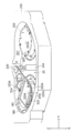
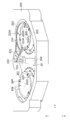
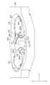
- FIG. 1 is a schematic plan view of a substrate processing apparatus according to an embodiment of the present invention. It is a schematic side view of the substrate processing apparatus shown by FIG. It is an expanded sectional view of the process chamber of the substrate processing apparatus shown by FIG.
- FIG. 4 is an enlarged perspective view of the processing chamber shown in FIG. 3. It is a principal part expansion perspective view which shows the temperature measurement part arrange
- FIG. 6 is a side view (left side view) of the temperature measurement unit shown in FIG. 5. It is an enlarged side view (enlarged side view of the code
- FIG. 5B is a left side view of the temperature measurement unit
- FIG. 5C is a right side view of the temperature measurement unit
- FIG. 4 is a plan view of the processing chamber shown in FIG. 3.
- FIG. 10 is a perspective view of a processing chamber corresponding to FIG. 9. It is an expansion perspective view corresponding to FIG. 4 explaining the 1st process of the substrate processing method concerning one embodiment. It is an expansion perspective view explaining a 2nd process. It is an expansion perspective view explaining a 3rd process. It is a figure which shows the relationship between the substrate heating time and substrate heating temperature explaining the substrate processing method which concerns on this Embodiment.
- the arrow X direction shown as appropriate indicates one direction in the horizontal direction
- the arrow Y direction indicates the other direction orthogonal to the arrow X direction in the horizontal direction
- An arrow Z direction indicates an upward direction orthogonal to the arrow X direction and the arrow Y direction.
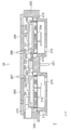
- the substrate processing apparatus 10 includes an atmospheric transfer chamber (EFEM: Equipment Front End Module) 12, load lock chambers 14 and 16, a transfer chamber 18, Processing chambers 20 and 22 are provided.
- the atmospheric transfer chamber 12, the load lock chambers 14 and 16, the transfer chamber 18, and the processing chambers 20 and 22 are sequentially arranged in the arrow Y direction.
- a carrier 26 for transporting a substrate 24 to be processed is disposed in the atmospheric transport chamber 12.
- a pod FOUP: Front Opening Unified Unified Pod
- the carrier 26 can store, for example, up to 25 substrates 24 at regular intervals in the vertical direction.
- An atmospheric robot 28 for transferring the substrate 24 is installed in the atmospheric transfer chamber 12 between the load lock chambers 14 and 16.
- a semiconductor wafer for manufacturing a semiconductor device such as a silicon wafer is used as the substrate 24.
- the load lock chambers 14 and 16 are both installed facing the atmospheric transfer chamber 12.
- one load lock chamber 14 is provided with a substrate support 140 that can accommodate, for example, 25 substrates 24 in the vertical direction at regular intervals.
- the substrate support 140 includes an upper plate 141 and a lower plate 142 that are arranged to face each other in the vertical direction, and a column 143 that connects the upper plate 141 and the lower plate 142.
- the substrate 24 is placed for each accommodation portion 144 and is accommodated in the substrate support 140.
- the support driving unit 145 raises and lowers the substrate support 140 in the direction of arrow A, and rotates the substrate support 140 in the horizontal direction of arrow B.
- the other load lock chamber 16 has the same configuration as the one load lock chamber 14.
- the transfer chamber 18 faces the opposite side of the load lock chambers 14, 16 from the atmospheric transfer chamber 12, and is installed on the virtual central axis C.
- a vacuum robot 180 for transferring the substrate 24 is installed between the load lock chambers 14 and 16 and between the processing chambers 20 and 22.
- the vacuum robot 180 includes an arm 181 having finger portions 182. Two arms 181 are provided here, although not shown.
- the finger portion 182 includes a lower finger 183 and an upper finger 184, and can transfer two upper and lower substrates 24 accommodated in the substrate support 140 simultaneously.
- the arm 181 moves the finger part 182 in the horizontal direction in the arrow D direction, and the arm driving part 185 rotates the arm 181 in the horizontal direction in the arrow E direction.
- the processing chambers 20 and 22 are installed facing the opposite side of the transfer chamber 18 from the load lock chambers 14 and 16.
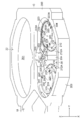
- One processing chamber 20 includes a reaction chamber 201.
- two substrate platforms (substrate platforms) 202 are provided in the same space of the reaction chamber 201 along the arrow Y direction.
- 203 are arranged.
- a partition unit 204 is disposed between the substrate platform 202 and the substrate platform 203, and the reaction chamber 201 can be partitioned by the partition unit 204.
- the other processing chamber 22 has the same configuration as the one processing chamber 20.
- the processing chambers 20 and 22 are mainly composed of, for example, aluminum. Note that the processing chambers 20 and 22 may be configured mainly with a metal or an alloy other than aluminum when the same function can be obtained.
- the substrate processing apparatus 10 includes a control unit 30.
- the control unit 30 is connected to each component of the substrate processing apparatus 10 such as the atmospheric transfer chamber 12 via the cable 32, and the entire operation of the substrate processing apparatus 10 is controlled by the control unit 30.
- the control unit 30 includes a storage medium and a computer (CPU).
- the substrate processing program stored in the storage medium is executed by the computer, and the operation of the substrate processing apparatus 10 is controlled.
- the storage medium for example, a hard disk, a semiconductor storage device (for example, RAM: “Random Access Memory”) or the like is used.
- Each component of the substrate processing apparatus 10 and the control unit 30 may be connected wirelessly.
- one processing chamber 20 includes a reaction chamber 201 formed in the reaction chamber body 200 in a semicircular shape in a plan view and in a concave shape in a side view. It is arranged.
- a prismatic partition 204 that crosses the arrow X direction is detachably disposed.
- substrate mounting portions 202 and 203 are disposed on both sides of the partition portion 204, respectively.
- the partition portion 204 is made of aluminum.
- the partition part 204 may be formed of quartz, aluminum oxide, or the like.
- One substrate 24 can be processed in the substrate platform 202, and another substrate 24 can be processed in the substrate platform 203. Therefore, two substrates 24 can be processed in the processing chamber 20.
- a lid 205 is disposed at a position corresponding to the substrate mounting portion 202 of the reaction chamber main body 200, and at a position corresponding to the substrate mounting portion 203 of the reaction chamber main body 200.
- a lid 206 is provided.
- a supply pipe 207 that communicates with the reaction chamber 201 from the outside is piped near the lid portion 205 of the reaction chamber main body 200, and similarly, a supply pipe that communicates with the reaction chamber 201 from the outside near the lid portion 206 of the reaction chamber main body 200.
- 208 is piped.
- the supply pipes 207 and 208 supply a gas for processing the substrate 24 from the outside into the reaction chamber 201.
- the reaction chamber 201 is connected to a vacuum pump (not shown), and a vacuum atmosphere of, for example, 0.1 Pa or less can be generated using this vacuum pump.
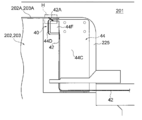
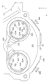
- One substrate mounting portion 202 has a cylindrical shape whose height is lower than the diameter.
- the upper surface of the substrate platform 202 on the lid 205 side is configured as a circular platform surface 202A on which the substrate 24 is placed.
- the height of the mounting surface 202A is set at a position lower than the height of the reaction chamber 201.
- a flange 202C that protrudes to the outer periphery is provided on the bottom 202B of the substrate platform 202, and the substrate platform 202 is supported by a column 209 through the flange 202C. As shown in FIGS. 3 and 4, the flange 202 ⁇ / b> C is fixed to the support column 209 using the fixing member 210, and the substrate placement unit 202 is attached to the reaction chamber main body 200.
- the other substrate platform 203 has a cylindrical shape, like the substrate platform 202.
- An upper surface on the lid 206 side of the substrate platform 203 is configured as a circular platform surface 203A on which the substrate 24 is placed.
- the height of the mounting surface 203 ⁇ / b> A is set at a position lower than the height of the reaction chamber 201.
- the bottom 203B of the substrate platform 203 is provided with a flange 203C that protrudes to the outer periphery, and the substrate platform 203 is supported by a column 209 via the flange 203C.
- the flange 203 ⁇ / b> C is fixed to the support column 209 using the fixing member 210, and the substrate placement unit 203 is attached to the reaction chamber main body 200.
- the substrate placement unit 202 includes a heating unit 211
- the substrate placement unit 203 includes a heating unit 211.
- a heater is used as the heating unit 211, and the heating unit 211 heats the substrate 24 placed on the placement surfaces 202A and 203A to a processing temperature.
- the processing temperature of the substrate 24 can be raised to, for example, 450 ° C. using the heating unit 211.
- the substrate mounting portion 202 is provided with a ring-shaped rectifying exhaust baffle ring 212 in a plan view surrounding the periphery of the side surface of the substrate mounting portion 202.
- a ring-shaped rectifying exhaust baffle ring 212 surrounding the side surface of the substrate platform 203 is disposed on the substrate platform 203.
- the rectifying exhaust baffle ring 212 is provided with a plurality of exhaust holes 212A penetrating in the plate thickness direction.
- a first exhaust port 213 is provided along the periphery of the side surface of the substrate platform 202 and further along the periphery of the side surface of the substrate platform 203, and the exhaust hole 212 ⁇ / b> A allows the exhaust gas after processing of the substrate 24 to pass through the first exhaust gas.
- the exhaust port 213 can be exhausted.
- the second exhaust port 214 and the third exhaust port 215 are sequentially arranged below the substrate mounting unit 202, and similarly, the second exhaust port 214, the second exhaust port 214 and the third exhaust port 215 are disposed below the substrate mounting unit 203. Each of the three exhaust ports 215 is sequentially arranged.
- the second exhaust port 214 is connected to the first exhaust port 213, and the third exhaust port 215 is connected to the second exhaust port 214.
- an exhaust path from the exhaust hole 212A to the third exhaust port 215 via the first exhaust port 213 and the second exhaust port 214 is constructed.
- a robot arm 220 as a transport mechanism is disposed in the reaction chamber 201.
- the robot arm 220 is configured to include a shaft portion 221 whose axial direction is the arrow Z direction and an arm 222 that transports the substrate 24.
- the shaft portion 221 has a two-axis configuration that rotates in the horizontal direction of the arrow F direction and rises and falls in the direction of the arrow G, and is connected to a drive unit that is not shown.
- the fingers 223 are formed in an arc shape having a radius larger than the radius of the substrate 24 and the radii of the substrate placement portions 202 and 203 in plan view.
- the finger 223 has a support portion (claw portion) 223A that protrudes from the one end portion, the intermediate portion, and the other end portion toward the center portion of the finger 223 and enters inside the periphery of the side surface of the substrate placement portions 202 and 203.
- the support portions 223A are formed at three positions of the fingers 223 at intervals of 120 degrees with the center portion of the fingers 223 as the center of the rotation angle.
- the finger 223 is made of alumina ceramics, for example.
- the substrate 24 is supported using the support part 223 ⁇ / b> A of the finger 223, and the substrate 24 transferred to the mounting surface 202 ⁇ / b> A of the substrate mounting unit 202 is transferred to the mounting surface 203 ⁇ / b> A of the substrate mounting unit 203. be able to.
- the substrate 24 transferred to the mounting surface 203A can be transferred (collected) to the mounting surface 202A after the substrate processing.
- the robot arm 220 and the partition unit 204 are disposed in the reaction chamber 201 and do not completely separate the space in the reaction chamber 201. That is, as shown in FIG. 3, the processing chamber 20 is configured to smoothly flow the gas supplied from the supply pipes 207 and 208 to the substrate 24 on the placement surface 202A and the substrate 24 on the placement surface 203A. It is said that. Further, the processing chamber 20 is configured to smoothly exhaust the exhaust gas after the substrate processing through each of the exhaust hole 212A, the first exhaust port 213, the second exhaust port 214, and the third exhaust hole 215.
- substrate holding pins 224 that move up and down in the vertical direction of the arrow Z direction are provided on the periphery of the mounting surface 202 ⁇ / b> A of the substrate mounting unit 202. As shown in FIG. 4, three substrate holding pins 224 are arranged at equal intervals on the periphery of the mounting surface 202 ⁇ / b> A here. Similarly, three substrate holding pins 224 are provided on the peripheral portion of the placement surface 203A of the substrate placement portion 203. The substrate holding pins 224 are configured to project on the mounting surface 202A or the mounting surface 203A and to transfer and mount the substrate 24.
- a storage portion 225 is disposed on the side surface portion of the substrate platform 202 at a position corresponding to the support portion 223A of the finger 223 in plan view.
- the storage unit 225 stores the support part 223A in the movement of the arm 222 in the direction perpendicular to the placement surface 202A, and prevents the support part 223A and the substrate placement part 202 from interfering with each other.
- the storage portion 225 has a U-shape that is substantially the same shape as the support portion 223A and is slightly larger in plan view, and has a vertical direction as a length direction (U-shape). (Notch part of shape).
- the number of storage portions 225 is set to the same number as the support portions 223A, and three storage portions 225 are provided here. On the other hand, a storage portion 225 is similarly disposed on the side surface portion of the substrate platform 203.
- the shape of the storage portion 225 is not particularly limited, and may be a groove (notch) such as a semicircular groove, a trapezoidal groove, a triangular groove, or a rectangular groove. If the number of support portions 223A is four or more, the number of storage portions 225 is also set to the same number (that is, four or more).
- the other processing chamber 22 has the same configuration as the one processing chamber 20, and thus the description thereof is omitted here.
- the storage unit 225 of the substrate platform 202 and the storage unit 225 of the substrate platform 203 include a temperature measurement unit (temperature measurement unit). 40 is disposed. At least one temperature measurement unit 40 is disposed on the substrate platform 202 and at least one temperature measurement unit 40 is disposed on the substrate platform 203. Note that three temperature measuring units 40 can be disposed on each of the substrate platform 202 and the substrate platform 203. More specifically, the temperature measuring unit 40 includes a temperature sensor 42 on which the tip 42A, which is a temperature detecting unit (temperature sensing unit), protrudes on the mounting surface 202A and the mounting surface 203A and is elastically deformable. An attachment member (base) 44 for attaching the temperature sensor 42 and fixing the temperature sensor 42 to the storage portion 225 is included.
- a temperature measurement unit temperature measurement unit
- thermocouple element is inserted into the heat-resistant metal tube, and the temperature sensor 42 is configured by a sheathed thermocouple in which the heat-resistant metal tube is filled with an inorganic insulator.
- the thermocouple element is inserted to the tip of the refractory metal tube, and the tip portion 42A, which is the tip of the refractory metal tube, constitutes a temperature detection unit (temperature sensing unit).
- the refractory metal tube is formed of, for example, a nickel alloy, and the diameter of the refractory metal tube is set to an extremely fine diameter of 0.5 mm or less, preferably 0.15 mm.
- the heat-resistant metal tube may be formed of stainless steel.
- the temperature sensor 42 is preferably thinner and has a smaller heat capacity because the smaller the heat capacity, the better the transient response.
- the protrusion amount d of the tip portion 42A of the temperature sensor 42 is set to 0.3 mm to 0.7 mm from the mounting surface 202A or the mounting surface 203A, and is set to 0.5 mm here. Yes.
- the protrusion amount d is set based on the deflection amount ⁇ of the tip end portion 42A of the temperature sensor 42, ease of attachment to the attachment member 44, adjustment of the protrusion amount d, and the like.
- the protruding direction of the tip 42A is the center direction of the mounting surface 202A or the mounting surface 203A and the arrow Z direction, and is 10 to 45 degrees with respect to the mounting surface 202A or the mounting surface 203A (horizontal plane). Here, it is inclined with an angle ⁇ of 30 degrees.
- the distal end portion 42A can be bent within the range of elastic deformation (within a range where plastic deformation is not performed).
- the attachment member 44 includes a bottom plate 44A, a pair of side wall plates 44B and a side wall that are provided upright from both ends of the bottom plate 44A.
- the plate 44C is provided and is formed in a U shape in a side view.
- the attachment member 44 is formed of, for example, a stainless steel plate, and the side wall plates 44B and 44C are formed by bending both end portions of the bottom plate 44A.
- the side wall plate 44B is fixed to one groove wall of the U groove of the storage portion 225, and the side wall plate 44C is fixed to the other groove wall of the U groove.
- the side wall plates 44B and 44C are accommodated in the storage portion 225 by the elastic force of the mounting member 44. It can fix so that it may press on the inner side of U-groove.
- a fixed portion 44D protruding toward the center of the mounting surface 202A or the mounting surface 203A is integrally formed on the upper portion of the side wall plate 44C, and the fixing portion 44D is bent toward the side wall plate 44B side to form the other side of the U groove. Spaced apart from the groove wall.
- the bottom plate 44A and the side wall plates 44B and 44C are each provided with a protruding portion 44G which is a protruding support portion.
- the bottom plate 44A and the side wall plates 44B and 44C are configured to be supported and fixed in contact with the U-groove of the storage portion 225 via the protrusion 44G.
- the front end portion 42A of the temperature sensor 42 is attached to the surface of the fixed portion 44D on the side wall plate 44B side.
- the distal end portion 42A is sandwiched and fixed between the fixing portion 44D and the holding plate 44E.
- the holding plate 44E is provided with a groove portion for holding the tip portion 42A, and the holding plate 44E is joined to the fixing portion 44D by welding in a state where the tip portion 42A is sandwiched between the groove portions. .
- the temperature sensor 42 is drawn downward along the side of the side wall plate 44C from the distal end portion 42A, and is sandwiched between the bottom plate 44A and the holding plate 44F at the intermediate portion.
- the holding plates 44E and 44F are made of, for example, a stainless steel sheet, and are joined to the fixed portion 44D and the bottom plate 44A by spot welding. As a result, the temperature sensor 42 can be fixed without causing thermal damage to the temperature sensor 42 that is formed very thin. As shown in FIGS. 9 and 10, the temperature sensor 42 is drawn out of the reaction chamber 201 through an output port 226 disposed on the side of the reaction chamber main body 200. The temperature sensor 42 is finally connected to the control unit 30 shown in FIG.
- the front end portion 42 ⁇ / b> A of the temperature sensor 42 contacts the back surface of the substrate 24, and the front end portion 42 ⁇ / b> A is caused by its own weight.
- the amount corresponding to the amount of protrusion d is bent.
- the distal end portion 42 ⁇ / b> A moves (elastically deforms) downward from the placement surface 202 ⁇ / b> A or the placement surface 203 ⁇ / b> A by being bent, and is stored in the storage portion 225.
- the front end portion 42A bends, so that the substrate 24 can be accurately placed on the placement surface 202A or the placement surface 203A without any gap.
- the tip end portion 42A and the back surface of the substrate 24 can always be brought into contact with each other.
- the tip portion 42 protrudes from the mounting surface 202A or 203A. There is no need to further provide a mechanism for fixing the substrate 24 to the placement surface 202A or 203A.
- the temperature measuring unit 40 is configured not to interfere with the support portion 223A when the finger 223 moves up and down.
- ⁇ PL 3 / 3EI (1)
- I ⁇ D 4/64 ... ( 2)
- the calculation condition is that the material of the heat-resistant metal tube of the temperature sensor 42 is, for example, a stainless steel material, the diameter of the substrate 24 is 300 mm, and the acting force P from the substrate 24 on the tip 42A is 1/5 of the mass of the substrate 24. .
- the deflection amount ⁇ is 0.5 [mm]
- the acting force P is 0.27 [N]
- the Young's modulus E is 200 ⁇ 10 3 [N / mm 2 ]
- the diameter D of the heat-resistant metal tube is 0.25 [mm].
- the length L is 5 [mm]. Considering the allowable range, the length L is set to 4 [mm] to 6 [mm].
- the substrate 24 is transferred from the carrier 26 in the atmospheric transfer chamber 12 shown in FIG. 1 to the load lock chambers 14 and 16 using the atmospheric robot 28.
- the substrate 24 is a semiconductor wafer used for manufacturing a semiconductor device.
- a semiconductor device is formed on the surface of the substrate 24.
- the transported substrate 24 is transported to and stored in the substrate support 140 shown in FIG.
- the substrate 24 accommodated in the substrate support 140 is transferred from the load lock chambers 14 and 16 to the processing chambers 20 and 22 shown in FIGS. 3 and 11 using the vacuum robot 180 in the transfer chamber 18 shown in FIG. It is transferred to the reaction chamber 201. Since the finger portion 182 of the vacuum robot 180 includes the lower finger 183 and the upper finger 184, two substrates 24 are simultaneously transferred onto the placement surface 202 ⁇ / b> A of the substrate placement portion 202 in the reaction chamber 201. Here, in FIGS. 11 to 13, the substrate 24 is not shown in order to clearly show the operation of the robot arm 220 and the like.
- the finger 223 of the robot arm 220 is waiting between the two substrates 24 transported onto the substrate platform 202.
- the substrate holding pins 224 (see FIG. 5) disposed on the peripheral portion of the mounting surface 202A of the substrate mounting unit 202 are raised, and the substrate 24 conveyed by the lower finger 183 of the vacuum robot 180 is transferred to the substrate. It is delivered to the holding pin 224.
- the finger 223 of the robot arm 220 rises in the direction of arrow G in conjunction with the rise of the substrate holding pin 224, and the substrate 24 transported by the upper finger 184 of the vacuum robot 180 is delivered to the support part 223A of the finger 223. It is.
- the finger portion 182 of the vacuum robot 180 is returned to the transfer chamber 18.
- the substrate holding pins 224 are lowered, and the substrate 24 transferred to the substrate holding pins 224 is placed on the placement surface 202A of the substrate placement portion 202.
- the temperature measuring unit 40 is disposed in the storage unit 225 of the substrate mounting unit 202, and the tip end part 42 ⁇ / b> A of the temperature sensor 42 of the temperature measuring unit 40 is mounted on the mounting surface. It protrudes on 202A. Therefore, when the substrate 24 is placed on the placement surface 202A, the tip portion 42A is in contact with the back surface of the substrate 24, and the tip portion 42A is in contact with the back surface of the substrate 24 due to its own weight. It is elastically deformed downward from the mounting surface 202A.
- the distal end portion 42 ⁇ / b> A is stored in the storage portion 225. And the temperature measurement of the board
- the substrate 24 delivered to the finger 223 is transferred onto the placement surface 203 ⁇ / b> A of the substrate placement unit 203 by the rotation of the robot arm 220 in the direction of arrow F. Then, as shown in FIG. 13, when the finger 223 is lowered in the direction of arrow G, the substrate 24 is placed on the placement surface 203 ⁇ / b> A of the substrate placement unit 203. At this time, the lowered support portion 223 ⁇ / b> A of the finger 223 is accommodated in the accommodating portion 225 provided in the substrate platform 203. Similarly, since the temperature measuring unit 40 is disposed in the substrate mounting unit 203, the temperature measurement of the substrate 24 mounted on the mounting surface 203A is started.
- the substrate 24 is placed on the placement surface 203A using the substrate holding pins 224 provided in the substrate placement portion 203. May be. Also in this case, the support portion 223 ⁇ / b> A of the finger 223 is accommodated in the accommodating portion 225 provided in the substrate platform 203.
- the substrate 24 placed on the placement surface 202A and the placement surface 203A is heated by the heating unit 211 shown in FIG.
- the substrate 24 is heated to 450 ° C., for example.
- gases necessary for the treatment of the substrate 24 are supplied from the supply pipes 207 and 208 to the reaction chamber 201.
- nitrogen (N 2 ) gas and oxygen (O 2 ) are supplied as gases, and an insulating protective film is formed on the surface of the substrate 24.
- N 2 nitrogen
- O 2 oxygen
- the temperature measurement method using the temperature measurement unit 40 of the present embodiment is a temperature of the substrate 24 heated to a temperature range that is difficult to measure in the non-contact temperature measurement method, for example, a temperature range of 500 ° C. or less. It can be particularly preferably used when measuring.
- the surface of the substrate 24 placed on the placement surface 202A and the placement surface 203A may be measured.
- an auxiliary heating unit may be disposed above the reaction chamber 201.
- the time to reach the processing temperature can be shortened, the heating efficiency can be improved, and the processing temperature range can be expanded.
- a high frequency coil may be disposed above the reaction chamber 201. The high-frequency coil is connected to a high-frequency power source, and plasma can be generated when a predetermined high-frequency power source is supplied to the high-frequency coil. By the generation of plasma, the substrate 24 can be subjected to an ashing process or a plasma CVD process.
- the substrate 24 is transferred from the reaction chamber 201 to the atmospheric transfer chamber 12 by a procedure reverse to the procedure transferred from the atmospheric transfer chamber 12 to the processing chambers 20 and 22.
- the transported substrate 24 is accommodated in a carrier 26.
- two substrates 24 are simultaneously processed in each of the reaction chamber 201 of the processing chamber 20 and the reaction chamber 201 of the processing chamber 22, but one substrate is processed in one reaction chamber 201.
- Substrate processing may be performed on the substrate 24.
- the substrate processing is executed by the computer of the control unit 30 according to the substrate processing program stored in the storage medium of the control unit 30 shown in FIG.
- the substrate processing apparatus 10 has a temperature sensor 42 that has an elastically deformable temperature sensor 42 that protrudes from the mounting surface 202A and is provided on the substrate mounting portion 202.
- a measurement unit 40 is provided.
- the tip 42A of the temperature sensor 42 contacts the back surface of the substrate 24 only by placing the substrate 24 on the mounting surface 202A, and the contact between the tip portion 42A and the back surface of the substrate 24 is ensured by bending due to elastic deformation. It will be something.
- the substrate processing apparatus 10 includes a temperature measuring unit 40 that includes an elastically deformable temperature sensor 42 that protrudes on the mounting surface 203A and is provided on the substrate mounting unit 203.
- the tip portion 42A of the temperature sensor 42 contacts the back surface of the substrate 24 only by placing the substrate 24 on the mounting surface 203A, and the tip portion 42A and the back surface of the substrate 24 are surely contacted by bending due to elastic deformation. It will be something. For this reason, the accuracy of temperature measurement of the substrate 24 can be easily improved regardless of the film formation state of the substrate 24.
- FIG. 14 shows the measurement result of the temperature of the substrate 24 using the temperature measurement unit 40 according to the present embodiment and the measurement result of the temperature according to the comparative example.
- the horizontal axis in FIG. 14 is the substrate heating time (second), and the vertical axis is the substrate heating temperature (° C.).
- the measurement result according to the comparative example is a temperature measurement result using a substrate with a thermocouple, and is indicated by a solid line.
- the measurement result of the temperature of the substrate 24 using the temperature measurement unit 40 is indicated by a broken line, and is substantially the same as the measurement result according to the comparative example. That is, according to the substrate processing apparatus 10 which concerns on this Embodiment, temperature can be measured with the high precision comparable to the board
- the tip end portion 42A of the temperature sensor 42 of the temperature measuring unit 40 is the surface of the substrate 24 placed on the placement surface 202A. It contacts the back surface and is stored below the mounting surface 202A by elastic deformation.
- the front end portion 42A of the temperature sensor 42 is in contact with the back surface of the substrate 24 placed on the placement surface 203A and is stored below the placement surface 203A by elastic deformation. Therefore, the temperature measuring unit 40 can measure the temperature with high accuracy using the temperature measuring unit 40 without hindering the mounting of the substrate 24 on the mounting surface 202A or the mounting surface 203A.
- the temperature sensor 42 of the temperature measuring unit 40 is configured by a sheath thermocouple in which a thermocouple element is inserted in a heat-resistant metal tube (see FIG. 7). For this reason, it is possible to measure the temperature with high accuracy by giving a deflection to the tip portion 42A of the temperature sensor 42 in particular.
- the heat-resistant metal tube of the sheath thermocouple is set to have a diameter of 0.5 mm or less.
- the heat capacity of the temperature sensor 42 is reduced, and the transient response of the temperature sensor 42 can be improved. For this reason, the temperature can be measured with high accuracy in a short time by using the temperature measuring unit 40.
- the protruding direction of the tip end portion 42A of the temperature sensor 42 is inclined with respect to the mounting surface 202A or the mounting surface 203A.
- the front end portion 42 ⁇ / b> A starts to be contacted from a state inclined to the back surface of the substrate 24, and thus is easily bent. That is, the distal end portion 42A is reliably brought into contact with the back surface of the substrate 24 by being bent, so that the temperature can be measured with high accuracy.
- the storage unit 225 that stores the support part 223 ⁇ / b> A of the finger 223 of the robot arm 220 as the transport mechanism is the substrate mounting unit 202, 203.
- the temperature sensor 42 of the temperature measurement unit 40 is disposed in the storage unit 225. For this reason, since the storage part 225 is utilized, the temperature measurement part 40 can be arrange
- the temperature measurement unit 40 attaches the temperature sensor 42 to the attachment member 44, and the attachment member 44 is accommodated in the storage portion 225. It is arranged by being fixed inside. For this reason, the temperature sensor 42 can be easily fixed to the storage portion 225 by the mounting member 44.
- the attachment member 44 is separated from the groove wall of the storage portion 225 of the substrate mounting portion 202 or 203.
- the temperature sensor 42 is attached to the fixing part 44D. For this reason, it is difficult for the temperature serving as measurement noise to be transmitted from the substrate platform 202 or 203 to the tip portion 42A of the temperature sensor 42 in particular, so that the temperature can be measured with high accuracy.
- the attachment member 44 since the attachment member 44 has a structure in which the U-groove of the storage portion 225 is brought into contact with and fixed through the projection 44G, heat transmitted from the substrate platform 202 or 203 to the temperature sensor 42 is reduced. be able to.
- the heating unit 211 is built in the substrate mounting units 202 and 203.
- the chamber 201 can be realized.
- the substrate processing method includes a step of placing the substrate 24 on the placement surface 202A of the substrate placement unit 202 or the placement surface 203A of the substrate placement unit 203.
- the temperature sensor 42 of the temperature measuring unit 40 protruding on the mounting surface 202A or the mounting surface 203A is brought into contact with the substrate 24 so as to be lower than the mounting surface 202A or the mounting surface 203A.
- a step of elastic deformation For this reason, since the contact between the tip end portion 42A of the temperature sensor 42 and the back surface of the substrate 24 is ensured, the accuracy of temperature measurement of the substrate 24 can be easily improved regardless of the film formation state of the substrate 24.
- the substrate processing method which can be provided can be provided.
- the substrate processing program, and the recording medium according to the present embodiment the same operational effects as those obtained by the substrate processing method according to the present embodiment can be obtained.
- the tip of the temperature sensor of the temperature measuring unit is formed with high rigidity that is difficult to deform, the tip is rotatable, and the tip protrudes onto the mounting surface using an elastic member such as a spring.
- You may comprise so that a state may be maintained. In this case, when the substrate is placed on the tip portion, the elastic member bends due to the weight of the substrate, so that the state where the tip portion is in contact with the back surface of the substrate is maintained.
- the temperature measurement unit may be disposed outside the substrate placement unit without using the storage unit of the finger support part.
- another concave portion (including through holes, notches, etc.) different from the storage portion of the finger support portion may be provided in the substrate mounting portion, and the temperature measuring portion may be disposed in the concave portion.
- the temperature sensor may be formed in a cylindrical coil shape (spiral shape) to have a spring property (elasticity) in the length direction of the column.
- the present invention it is possible to provide a technique capable of easily improving the accuracy of temperature measurement of a substrate regardless of the film formation state of the substrate.
- Substrate processing device 20 20, 22 Processing chamber 24 24 Substrate 203 202, 203 Substrate placement part 223 Finger 223A Support part 2 225 Storage part 40 40 Temperature measurement part 42 Temperature sensor 44 44 Attachment member
Abstract
Description
図1及び図2に示されるように、本実施の形態に係る基板処理装置10は、大気搬送室(EFEM:Equipment Front End Module)12と、ロードロック室14、16と、搬送室18と、処理室20及び22とを備えている。これらの大気搬送室12、ロードロック室14、16、搬送室18、処理室20及び22は、矢印Y方向に向かって順次配設されている。 [Overall schematic configuration of substrate processing apparatus]
As shown in FIGS. 1 and 2, the
次に、上記処理室20、22について、詳しく説明する。図1、図3及び図4に示されるように、一方の処理室20には、反応室本体200に平面視において半円形状に形成され、側面視において凹形状に形成された反応室201が配設されている。反応室201の矢印Y方向中間部には、矢印X方向に横切る角柱形状の仕切部204が着脱自在に配置されている。反応室201では仕切部204を中心として両側のそれぞれに基板載置部202、203が配設されている。仕切部204は、ここではアルミニウムにより形成されている。また、仕切部204は、石英、酸化アルミニウム等により形成されてもよい。基板載置部202において1枚の基板24を処理することができ、基板載置部203において他の1枚の基板24を処理することができる。従って、処理室20では2枚の基板24を処理することができる。 [Detailed configuration of processing chamber]
Next, the
図5~図7に示されるように、処理室20、22のそれぞれにおいて、基板載置部202の収納部225及び基板載置部203の収納部225には、温度測定部(温度測定ユニット)40が配設されている。温度測定部40は、基板載置部202に少なくとも1個、基板載置部203に少なくとも1個配設されている。なお、基板載置部202、基板載置部203にはそれぞれ3個の温度測定部40が配設可能である。詳しく説明すると、温度測定部40は、載置面202A上、載置面203A上に温度検出部(温感部)である先端部42Aが突出し、かつ、弾性変形可能な温度センサ42と、この温度センサ42を取付けて収納部225に固定する取付部材(土台)44とを含んで構成されている。 [Detailed configuration of temperature measurement unit]
As shown in FIGS. 5 to 7, in each of the
δ=PL3/3EI …(1)
I=πD4/64 …(2)
算出条件は、温度センサ42の耐熱金属管の材料を例えばステンレス鋼材とし、基板24の直径を300mmとし、先端部42Aにかかる基板24からの作用力Pを基板24の質量の1/5とする。撓み量δは0.5[mm]、作用力Pは0.27[N]、ヤング係数Eは200×103[N/mm2]、耐熱金属管の直径Dは0.25[mm]とすると、長さLは5[mm]となる。許容範囲を考慮し、長さLは4[mm]~6[mm]に設定される。 Here, the length (span length) L from the attachment position of the
δ = PL 3 / 3EI (1)
I = πD 4/64 ... ( 2)
The calculation condition is that the material of the heat-resistant metal tube of the
次に、上記基板処理装置10を用いた基板処理方法を説明し、併せて半導体装置の製造方法並びに基板処理プログラムを説明する。基板処理装置10では、図1に示される大気搬送室12のキャリア26から大気ロボット28を用いてロードロック室14、16に基板24が搬送される。基板24は半導体装置を製造するために用いられる半導体ウェーハである。例えば基板24の面上に半導体装置が形成される。搬送された基板24は、図2に示される基板支持体140に搬送され、かつ、収納される。 [Substrate Processing Method, Semiconductor Device Manufacturing Method, and Substrate Processing Program]
Next, a substrate processing method using the
なお、載置面202A上に基板24を載置する場合と同様に、基板載置部203に設けられた基板保持ピン224を用いて、基板24を載置面203A上に載置させるようにしてもよい。この場合も、フィンガー223の支持部位223Aは、基板載置部203に設けられた収納部225内に収容される。 On the other hand, as shown in FIG. 12, the
As in the case where the
本実施の形態に係る基板処理装置10は、図5~図8に示されるように、載置面202A上に突出して基板載置部202に設けられた弾性変形可能な温度センサ42を有する温度測定部40を備える。温度センサ42の先端部42Aは載置面202A上に基板24を載置するだけで基板24の裏面に接触し、弾性変形により撓むことにより先端部42Aと基板24の裏面との接触が確実なものとなる。同様に、基板処理装置10は、載置面203A上に突出して基板載置部203に設けられた弾性変形可能な温度センサ42を有する温度測定部40を備える。温度センサ42の先端部42Aは載置面203A上に基板24を載置するだけで基板24の裏面に接触し、弾性変形により撓むことにより先端部42Aと基板24の裏面との接触が確実なものとなる。このため、基板24の成膜状態にかかわらず、基板24の温度測定の精度を簡易に向上させることができる。 (Operation and effect of the present embodiment)
The
本発明は、上記実施の形態に限定されるものではなく、その要旨を逸脱しない範囲において、種々変形可能である。例えば、本発明は、温度測定部の温度センサの先端部を変形し難い高い剛性により形成し、先端部を回動可能とし、ばね等の弾性部材を用いて載置面上に先端部の突出状態を維持するように構成してもよい。この場合、先端部の上に基板が載置されると、基板の自重により弾性部材が撓むことにより、先端部が基板裏面に接触した状態が維持される。 (Other embodiments)
The present invention is not limited to the above embodiment, and various modifications can be made without departing from the scope of the invention. For example, according to the present invention, the tip of the temperature sensor of the temperature measuring unit is formed with high rigidity that is difficult to deform, the tip is rotatable, and the tip protrudes onto the mounting surface using an elastic member such as a spring. You may comprise so that a state may be maintained. In this case, when the substrate is placed on the tip portion, the elastic member bends due to the weight of the substrate, so that the state where the tip portion is in contact with the back surface of the substrate is maintained.
Claims (16)
- 載置面を有し、当該載置面に基板が載置される基板載置部と、
前記載置面に載置される前記基板を加熱する加熱部と、
先端が温度検出部を構成する弾性変形可能な温度センサと、を備え、
前記温度センサは前記載置面の下から前記載置面の上まで延びており、前記先端が前記載置面から突出している、
基板処理装置。 A substrate mounting portion having a mounting surface, on which the substrate is mounted;
A heating unit that heats the substrate placed on the placement surface;
An elastically deformable temperature sensor whose tip constitutes a temperature detection unit,
The temperature sensor extends from below the placement surface to above the placement surface, and the tip projects from the placement surface.
Substrate processing equipment. - 前記温度センサは、前記載置面に前記基板が載置されると、前記先端が前記基板の裏面に接触するとともに、前記載置面から突出する部分が前記載置面の下に収まるように弾性変形するように構成されている、請求項1記載の基板処理装置。 The temperature sensor is configured such that when the substrate is placed on the placement surface, the tip is in contact with the back surface of the substrate, and a portion protruding from the placement surface is placed below the placement surface. The substrate processing apparatus according to claim 1, wherein the substrate processing apparatus is configured to be elastically deformed.
- 前記温度センサはシース熱電対により構成される、請求項1記載の基板処理装置。 The substrate processing apparatus according to claim 1, wherein the temperature sensor is configured by a sheath thermocouple.
- 前記温度センサは、前記載置面に前記基板が載置されると、前記基板の自重のみによって弾性変形して前記載置面から突出する部分が前記載置面の下に収まるように構成されている、請求項2記載の基板処理装置。 The temperature sensor is configured such that when the substrate is placed on the placement surface, a portion protruding from the placement surface by being elastically deformed only by the weight of the substrate fits under the placement surface. The substrate processing apparatus according to claim 2.
- 前記温度センサは、前記シース熱電対自体が弾性変形するように構成されている、請求項3記載の基板処理装置。 The substrate processing apparatus according to claim 3, wherein the temperature sensor is configured such that the sheath thermocouple itself is elastically deformed.
- 前記温度センサはシース熱電対により構成される、請求項2記載の基板処理装置。 The substrate processing apparatus according to claim 2, wherein the temperature sensor is configured by a sheath thermocouple.
- 前記温度センサは、前記載置面に前記基板が載置されると、前記シース熱電対自体が弾性変形するように構成されている、請求項6記載の基板処理装置。 The substrate processing apparatus according to claim 6, wherein the temperature sensor is configured such that when the substrate is placed on the placement surface, the sheath thermocouple itself is elastically deformed.
- 前記シース熱電対の直径は0.5mm以下である、請求項3記載の基板処理装置。 The substrate processing apparatus according to claim 3, wherein a diameter of the sheath thermocouple is 0.5 mm or less.
- 前記シース熱電対の前記載置面から突出する部分は、前記載置面に対して傾斜するように設けられる、請求項3記載の基板処理装置。 4. The substrate processing apparatus according to claim 3, wherein a portion of the sheath thermocouple protruding from the placement surface is provided so as to be inclined with respect to the placement surface.
- 前記基板を保持可能なアームを備え、前記アームにより保持された前記基板を前記載置面上に搬送することができるように構成された基板搬送機構を有し、
前記基板載置部は、前記アームの少なくとも一部が収容されるように構成される凹部又は切欠部を備え、
前記先端は、前記凹部又は切欠部の内側から前記載置面の上に突出するように設けられる、請求項3記載の基板処理装置。 An arm that can hold the substrate; and a substrate transport mechanism configured to transport the substrate held by the arm onto the placement surface.
The substrate mounting portion includes a recess or a notch configured to accommodate at least a part of the arm,
The substrate processing apparatus according to claim 3, wherein the tip is provided so as to protrude from the inside of the recess or notch onto the mounting surface. - 前記温度センサの検出部は、前記基板載置部に設けられた凹部、切欠部、又は貫通孔の何れかの内側から前記載置面の上に突出するように設けられ、
前記凹部、切欠部、又は貫通孔の何れかの内側には、前記温度センサが固定されるように構成される取付部材が設けられ、
前記取付部材は、突起状の支持部を備え、前記取付部材は前記支持部を介して前記基板載置部に対して固定されるように構成される、請求項1記載の基板処理装置。 The detection part of the temperature sensor is provided so as to protrude from the inner side of any one of the recess, the notch, or the through hole provided in the substrate placement part,
An attachment member configured to fix the temperature sensor is provided inside any one of the recess, the notch, or the through hole,
The substrate processing apparatus according to claim 1, wherein the attachment member includes a projecting support portion, and the attachment member is configured to be fixed to the substrate mounting portion via the support portion. - 前記加熱部は前記基板載置部内に設けられている、請求項11記載の基板処理装置。 The substrate processing apparatus according to claim 11, wherein the heating unit is provided in the substrate mounting unit.
- 基板が載置される載置面を有する基板載置部に取り付けられる温度測定ユニットであって、
前記温度測定ユニットは、
先端が温度検出部を構成する弾性変形可能な温度センサ、を備え、
前記温度センサは前記載置面の下から前記載置面の上まで延びており、前記先端が前記載置面から突出している。 A temperature measuring unit attached to a substrate mounting portion having a mounting surface on which a substrate is mounted,
The temperature measurement unit includes:
An elastically deformable temperature sensor whose tip constitutes a temperature detector,
The temperature sensor extends from below the placement surface to above the placement surface, and the tip projects from the placement surface. - 前記温度センサはシース熱電対により構成される、請求項13記載の温度測定ユニット。 The temperature measurement unit according to claim 13, wherein the temperature sensor is configured by a sheath thermocouple.
- 基板載置部の載置面に基板を載置し、かつ、前記載置面上に突出する温度センサの先端を前記基板裏面に接触させて、前記先端を前記載置面よりも下方に押し下げるように前記温度センサを弾性変形させる工程と、
前記基板を加熱する工程と、
前記温度センサを用いて前記基板の温度を測定する工程と、
を備えた半導体装置の製造方法。 The substrate is placed on the placement surface of the substrate placement portion, and the tip of the temperature sensor protruding on the placement surface is brought into contact with the back surface of the substrate, and the tip is pushed down below the placement surface. The step of elastically deforming the temperature sensor,
Heating the substrate;
Measuring the temperature of the substrate using the temperature sensor;
A method for manufacturing a semiconductor device comprising: - 前記温度センサは、先端に温度検出部を有するシース熱電対により構成されている、請求項15記載の半導体装置の製造方法。 16. The method of manufacturing a semiconductor device according to claim 15, wherein the temperature sensor is configured by a sheath thermocouple having a temperature detection unit at a tip.
Priority Applications (4)
| Application Number | Priority Date | Filing Date | Title |
|---|---|---|---|
| KR1020187026944A KR102219361B1 (en) | 2016-03-28 | 2017-01-25 | Substrate processing apparatus, temperature measuring unit, and manufacturing method of semiconductor device |
| CN201780015489.1A CN108780753B (en) | 2016-03-28 | 2017-01-25 | Substrate processing apparatus, temperature measuring unit, and method for manufacturing semiconductor device |
| JP2018508450A JP6513285B2 (en) | 2016-03-28 | 2017-01-25 | Substrate processing apparatus and method of manufacturing semiconductor device |
| US16/133,058 US11424146B2 (en) | 2016-03-28 | 2018-09-17 | Substrate processing apparatus and temperature measurement unit |
Applications Claiming Priority (2)
| Application Number | Priority Date | Filing Date | Title |
|---|---|---|---|
| JP2016063144 | 2016-03-28 | ||
| JP2016-063144 | 2016-03-28 |
Related Child Applications (1)
| Application Number | Title | Priority Date | Filing Date |
|---|---|---|---|
| US16/133,058 Continuation US11424146B2 (en) | 2016-03-28 | 2018-09-17 | Substrate processing apparatus and temperature measurement unit |
Publications (1)
| Publication Number | Publication Date |
|---|---|
| WO2017169032A1 true WO2017169032A1 (en) | 2017-10-05 |
Family
ID=59964127
Family Applications (1)
| Application Number | Title | Priority Date | Filing Date |
|---|---|---|---|
| PCT/JP2017/002535 WO2017169032A1 (en) | 2016-03-28 | 2017-01-25 | Substrate-processing device, temperature-measuring unit, and method for manufacturing semiconductor device |
Country Status (6)
| Country | Link |
|---|---|
| US (1) | US11424146B2 (en) |
| JP (1) | JP6513285B2 (en) |
| KR (1) | KR102219361B1 (en) |
| CN (1) | CN108780753B (en) |
| TW (1) | TWI633602B (en) |
| WO (1) | WO2017169032A1 (en) |
Families Citing this family (3)
| Publication number | Priority date | Publication date | Assignee | Title |
|---|---|---|---|---|
| JP6579974B2 (en) * | 2015-02-25 | 2019-09-25 | 株式会社Kokusai Electric | Substrate processing apparatus, temperature sensor, and semiconductor device manufacturing method |
| TWI676012B (en) * | 2018-10-19 | 2019-11-01 | 國立彰化師範大學 | Air flow heat conduction measurement system |
| US20230205287A1 (en) * | 2021-12-28 | 2023-06-29 | Ati Technologies Ulc | Processing unit reset by a virtual function |
Citations (4)
| Publication number | Priority date | Publication date | Assignee | Title |
|---|---|---|---|---|
| JPS63227013A (en) * | 1987-03-02 | 1988-09-21 | バルツァース・アクチェンゲゼルシャフト | Semiconductor wafer treating equipment |
| JPH1048063A (en) * | 1996-08-07 | 1998-02-20 | Sony Corp | Fluorescent thermometer |
| JP2013033946A (en) * | 2011-07-01 | 2013-02-14 | Hitachi Kokusai Electric Inc | Substrate processing apparatus and manufacturing method of semiconductor device |
| JP2015059833A (en) * | 2013-09-19 | 2015-03-30 | 株式会社アンベエスエムティ | Thermocouple for surface temperature measurement and surface temperature measurement device |
Family Cites Families (7)
| Publication number | Priority date | Publication date | Assignee | Title |
|---|---|---|---|---|
| EP0915499B1 (en) * | 1997-11-05 | 2011-03-23 | Tokyo Electron Limited | Semiconductor wafer holding apparatus |
| US6572265B1 (en) * | 2001-04-20 | 2003-06-03 | Luxtron Corporation | In situ optical surface temperature measuring techniques and devices |
| US20060275933A1 (en) * | 2005-06-02 | 2006-12-07 | Applied Materials, Inc. | Thermally conductive ceramic tipped contact thermocouple |
| JP2007042911A (en) * | 2005-08-04 | 2007-02-15 | Sumitomo Electric Ind Ltd | Wafer holder and wafer prober mounted with the same |
| JP5197505B2 (en) * | 2009-06-19 | 2013-05-15 | 東京エレクトロン株式会社 | Temperature sensor for wafer chuck |
| JP5195711B2 (en) * | 2009-10-13 | 2013-05-15 | 東京エレクトロン株式会社 | Substrate cooling device, substrate cooling method, and storage medium |
| JP2011221006A (en) * | 2010-03-23 | 2011-11-04 | Tokyo Electron Ltd | Wafer type temperature detection sensor and method of manufacturing the same |
-
2017
- 2017-01-25 JP JP2018508450A patent/JP6513285B2/en active Active
- 2017-01-25 WO PCT/JP2017/002535 patent/WO2017169032A1/en active Application Filing
- 2017-01-25 CN CN201780015489.1A patent/CN108780753B/en active Active
- 2017-01-25 KR KR1020187026944A patent/KR102219361B1/en active IP Right Grant
- 2017-02-21 TW TW106105733A patent/TWI633602B/en active
-
2018
- 2018-09-17 US US16/133,058 patent/US11424146B2/en active Active
Patent Citations (4)
| Publication number | Priority date | Publication date | Assignee | Title |
|---|---|---|---|---|
| JPS63227013A (en) * | 1987-03-02 | 1988-09-21 | バルツァース・アクチェンゲゼルシャフト | Semiconductor wafer treating equipment |
| JPH1048063A (en) * | 1996-08-07 | 1998-02-20 | Sony Corp | Fluorescent thermometer |
| JP2013033946A (en) * | 2011-07-01 | 2013-02-14 | Hitachi Kokusai Electric Inc | Substrate processing apparatus and manufacturing method of semiconductor device |
| JP2015059833A (en) * | 2013-09-19 | 2015-03-30 | 株式会社アンベエスエムティ | Thermocouple for surface temperature measurement and surface temperature measurement device |
Also Published As
| Publication number | Publication date |
|---|---|
| JP6513285B2 (en) | 2019-05-15 |
| KR102219361B1 (en) | 2021-02-23 |
| TW201802941A (en) | 2018-01-16 |
| US20190019699A1 (en) | 2019-01-17 |
| KR20180118682A (en) | 2018-10-31 |
| CN108780753A (en) | 2018-11-09 |
| TWI633602B (en) | 2018-08-21 |
| JPWO2017169032A1 (en) | 2018-12-27 |
| US11424146B2 (en) | 2022-08-23 |
| CN108780753B (en) | 2023-04-25 |
Similar Documents
| Publication | Publication Date | Title |
|---|---|---|
| US11049742B2 (en) | Substrate processing apparatus, method of manufacturing semiconductor device, and thermocouple support | |
| US9269638B2 (en) | Temperature detecting apparatus, substrate processing apparatus and method of manufacturing semiconductor device | |
| TWI458946B (en) | Thermocouple | |
| WO2017169032A1 (en) | Substrate-processing device, temperature-measuring unit, and method for manufacturing semiconductor device | |
| JP5902085B2 (en) | Apparatus for positioning a substrate in a processing chamber and method for centering a substrate in the processing chamber | |
| US20090052498A1 (en) | Thermocouple | |
| US20030231698A1 (en) | Apparatus and method for fabricating a semiconductor device and a heat treatment apparatus | |
| WO2006030857A1 (en) | Heat treatment apparatus and substrate manufacturing method | |
| US20120160419A1 (en) | Substrate-supporting unit and substrate-processing apparatus comprising same | |
| US20130167772A1 (en) | Film forming apparatus | |
| JPH0451538A (en) | Temperature measuring instrument for plate like object | |
| CN110400772B (en) | Electrostatic chuck and semiconductor processing equipment | |
| JP2012054408A (en) | Substrate treatment apparatus and method for manufacturing substrate to be treated | |
| JP2007134518A (en) | Heat treatment apparatus | |
| TW202220082A (en) | Apparatus, system, and method for non-contact temperature monitoring of substrate supports | |
| JP2004022943A (en) | Semiconductor manufacturing equipment | |
| JP2001237193A (en) | Wafer boat for heat-treating device and heat-treating method | |
| JP2009088395A (en) | Substrate processing apparatus | |
| JP2002353111A (en) | Temperature control method of heat treatment plate and heat treatment apparatus | |
| KR20230064169A (en) | Appratus for measuring temperature, and apparatus for processing substrate having the same | |
| JP2010056108A (en) | Process monitoring method, mass measuring method, and device | |
| US8373097B2 (en) | Apparatus for thermally processing substrate | |
| JP2008282858A (en) | Pin for supporting substrate | |
| JP2003249456A (en) | Substrate treating apparatus | |
| KR20060101591A (en) | Apparatus for manufacturing a semiconductor substrate |
Legal Events
| Date | Code | Title | Description |
|---|---|---|---|
| WWE | Wipo information: entry into national phase |
Ref document number: 2018508450 Country of ref document: JP |
|
| ENP | Entry into the national phase |
Ref document number: 20187026944 Country of ref document: KR Kind code of ref document: A |
|
| NENP | Non-entry into the national phase |
Ref country code: DE |
|
| 121 | Ep: the epo has been informed by wipo that ep was designated in this application |
Ref document number: 17773582 Country of ref document: EP Kind code of ref document: A1 |
|
| 122 | Ep: pct application non-entry in european phase |
Ref document number: 17773582 Country of ref document: EP Kind code of ref document: A1 |