WO2017168630A1 - Flaw inspection device and flaw inspection method - Google Patents
Flaw inspection device and flaw inspection method Download PDFInfo
- Publication number
- WO2017168630A1 WO2017168630A1 PCT/JP2016/060375 JP2016060375W WO2017168630A1 WO 2017168630 A1 WO2017168630 A1 WO 2017168630A1 JP 2016060375 W JP2016060375 W JP 2016060375W WO 2017168630 A1 WO2017168630 A1 WO 2017168630A1
- Authority
- WO
- WIPO (PCT)
- Prior art keywords
- defect
- value
- determination unit
- inspection apparatus
- unit
- Prior art date
Links
- 238000007689 inspection Methods 0.000 title claims abstract description 80
- 238000000034 method Methods 0.000 title claims description 26
- 238000000605 extraction Methods 0.000 claims abstract description 79
- 238000001514 detection method Methods 0.000 claims abstract description 46
- 238000011156 evaluation Methods 0.000 claims abstract description 20
- 230000007547 defect Effects 0.000 claims description 290
- 239000000284 extract Substances 0.000 claims description 16
- 230000002950 deficient Effects 0.000 claims description 8
- 238000010606 normalization Methods 0.000 claims description 5
- 230000007423 decrease Effects 0.000 claims description 2
- 238000003384 imaging method Methods 0.000 claims 2
- 238000005516 engineering process Methods 0.000 abstract 1
- 230000035945 sensitivity Effects 0.000 description 21
- 238000010586 diagram Methods 0.000 description 15
- 238000012545 processing Methods 0.000 description 13
- 238000005286 illumination Methods 0.000 description 11
- 230000003287 optical effect Effects 0.000 description 9
- 230000008569 process Effects 0.000 description 8
- 230000006870 function Effects 0.000 description 7
- 239000004065 semiconductor Substances 0.000 description 7
- 230000005856 abnormality Effects 0.000 description 4
- 230000008859 change Effects 0.000 description 2
- 238000004891 communication Methods 0.000 description 2
- 238000012937 correction Methods 0.000 description 2
- 238000012986 modification Methods 0.000 description 2
- 230000004048 modification Effects 0.000 description 2
- 238000005457 optimization Methods 0.000 description 2
- 230000009471 action Effects 0.000 description 1
- 239000002131 composite material Substances 0.000 description 1
- 230000003247 decreasing effect Effects 0.000 description 1
- 239000006185 dispersion Substances 0.000 description 1
- 230000002093 peripheral effect Effects 0.000 description 1
- 230000010287 polarization Effects 0.000 description 1
- 238000012552 review Methods 0.000 description 1
- 238000001878 scanning electron micrograph Methods 0.000 description 1
- 239000007787 solid Substances 0.000 description 1
- 238000012360 testing method Methods 0.000 description 1
- 238000012795 verification Methods 0.000 description 1
Images


Classifications
-
- G—PHYSICS
- G01—MEASURING; TESTING
- G01N—INVESTIGATING OR ANALYSING MATERIALS BY DETERMINING THEIR CHEMICAL OR PHYSICAL PROPERTIES
- G01N21/00—Investigating or analysing materials by the use of optical means, i.e. using sub-millimetre waves, infrared, visible or ultraviolet light
- G01N21/84—Systems specially adapted for particular applications
- G01N21/88—Investigating the presence of flaws or contamination
- G01N21/95—Investigating the presence of flaws or contamination characterised by the material or shape of the object to be examined
- G01N21/956—Inspecting patterns on the surface of objects
-
- G—PHYSICS
- G01—MEASURING; TESTING
- G01N—INVESTIGATING OR ANALYSING MATERIALS BY DETERMINING THEIR CHEMICAL OR PHYSICAL PROPERTIES
- G01N21/00—Investigating or analysing materials by the use of optical means, i.e. using sub-millimetre waves, infrared, visible or ultraviolet light
- G01N21/84—Systems specially adapted for particular applications
- G01N21/88—Investigating the presence of flaws or contamination
- G01N21/8851—Scan or image signal processing specially adapted therefor, e.g. for scan signal adjustment, for detecting different kinds of defects, for compensating for structures, markings, edges
-
- G—PHYSICS
- G01—MEASURING; TESTING
- G01N—INVESTIGATING OR ANALYSING MATERIALS BY DETERMINING THEIR CHEMICAL OR PHYSICAL PROPERTIES
- G01N21/00—Investigating or analysing materials by the use of optical means, i.e. using sub-millimetre waves, infrared, visible or ultraviolet light
- G01N21/84—Systems specially adapted for particular applications
- G01N21/88—Investigating the presence of flaws or contamination
- G01N21/8806—Specially adapted optical and illumination features
-
- G—PHYSICS
- G01—MEASURING; TESTING
- G01N—INVESTIGATING OR ANALYSING MATERIALS BY DETERMINING THEIR CHEMICAL OR PHYSICAL PROPERTIES
- G01N21/00—Investigating or analysing materials by the use of optical means, i.e. using sub-millimetre waves, infrared, visible or ultraviolet light
- G01N21/84—Systems specially adapted for particular applications
- G01N21/88—Investigating the presence of flaws or contamination
- G01N21/95—Investigating the presence of flaws or contamination characterised by the material or shape of the object to be examined
- G01N21/9501—Semiconductor wafers
-
- G—PHYSICS
- G05—CONTROLLING; REGULATING
- G05B—CONTROL OR REGULATING SYSTEMS IN GENERAL; FUNCTIONAL ELEMENTS OF SUCH SYSTEMS; MONITORING OR TESTING ARRANGEMENTS FOR SUCH SYSTEMS OR ELEMENTS
- G05B19/00—Programme-control systems
- G05B19/02—Programme-control systems electric
- G05B19/418—Total factory control, i.e. centrally controlling a plurality of machines, e.g. direct or distributed numerical control [DNC], flexible manufacturing systems [FMS], integrated manufacturing systems [IMS] or computer integrated manufacturing [CIM]
- G05B19/41875—Total factory control, i.e. centrally controlling a plurality of machines, e.g. direct or distributed numerical control [DNC], flexible manufacturing systems [FMS], integrated manufacturing systems [IMS] or computer integrated manufacturing [CIM] characterised by quality surveillance of production
-
- H—ELECTRICITY
- H01—ELECTRIC ELEMENTS
- H01L—SEMICONDUCTOR DEVICES NOT COVERED BY CLASS H10
- H01L22/00—Testing or measuring during manufacture or treatment; Reliability measurements, i.e. testing of parts without further processing to modify the parts as such; Structural arrangements therefor
- H01L22/10—Measuring as part of the manufacturing process
-
- G—PHYSICS
- G01—MEASURING; TESTING
- G01N—INVESTIGATING OR ANALYSING MATERIALS BY DETERMINING THEIR CHEMICAL OR PHYSICAL PROPERTIES
- G01N2201/00—Features of devices classified in G01N21/00
- G01N2201/06—Illumination; Optics
- G01N2201/061—Sources
-
- H—ELECTRICITY
- H01—ELECTRIC ELEMENTS
- H01L—SEMICONDUCTOR DEVICES NOT COVERED BY CLASS H10
- H01L22/00—Testing or measuring during manufacture or treatment; Reliability measurements, i.e. testing of parts without further processing to modify the parts as such; Structural arrangements therefor
- H01L22/10—Measuring as part of the manufacturing process
- H01L22/12—Measuring as part of the manufacturing process for structural parameters, e.g. thickness, line width, refractive index, temperature, warp, bond strength, defects, optical inspection, electrical measurement of structural dimensions, metallurgic measurement of diffusions
-
- Y—GENERAL TAGGING OF NEW TECHNOLOGICAL DEVELOPMENTS; GENERAL TAGGING OF CROSS-SECTIONAL TECHNOLOGIES SPANNING OVER SEVERAL SECTIONS OF THE IPC; TECHNICAL SUBJECTS COVERED BY FORMER USPC CROSS-REFERENCE ART COLLECTIONS [XRACs] AND DIGESTS
- Y02—TECHNOLOGIES OR APPLICATIONS FOR MITIGATION OR ADAPTATION AGAINST CLIMATE CHANGE
- Y02P—CLIMATE CHANGE MITIGATION TECHNOLOGIES IN THE PRODUCTION OR PROCESSING OF GOODS
- Y02P90/00—Enabling technologies with a potential contribution to greenhouse gas [GHG] emissions mitigation
- Y02P90/02—Total factory control, e.g. smart factories, flexible manufacturing systems [FMS] or integrated manufacturing systems [IMS]
Definitions
- the present invention relates to a technique for inspecting a defect of an inspection object.
- Patent Document 1 states: “Detect and analyze the characteristics of the test piece to identify defects having level information.
- the inspection system analyzes level information using a set of initial thresholds of system parameters and catches an initial part of an abnormality as a defect.
- An overview of the captured defects is displayed, and an operating curve of the potentially captured defects for the threshold parameter is also displayed.
- the parameter is selectively changed to form a correction threshold, and the abnormality threshold information is analyzed using the correction threshold.
- the updated part of the abnormality is caught as a defect, and an outline of the caught abnormality is displayed together with the recalculated operation curve.
- the step of selectively changing the threshold and recapturing the defects is repeated as desired to store a modified set of threshold parameters for use in the inspection system recipe. ”(See summary).
- threshold parameters are individually optimized by identifying defects by individually changing a plurality of threshold parameters and displaying an operation curve.
- the present invention has been made in view of the above problems, and an object of the present invention is to provide a defect inspection technique capable of setting parameters used for detecting defects with a small burden on the user.
- the defect inspection apparatus receives a plurality of reference values input by a user and calculates defect extraction conditions so that an evaluation value calculated using the reference value / actual report number / false report number is optimal. To do.
- the user can obtain effective defect extraction conditions only by inputting a reference value. Thereby, the burden which sets a defect extraction parameter for a user can be suppressed.
- FIG. 1 is a configuration diagram of a defect inspection apparatus 100 according to Embodiment 1.
- FIG. 3 is a top view illustrating an example of a sample 110.
- FIG. It is a block diagram of the internal calculation block with which the image process part 210 is provided.
- 3 is a block diagram illustrating an internal configuration of a defect determination unit 220.
- FIG. 3 is a block diagram showing an internal configuration of a space classifier 222.
- FIG. It is an example of the defect candidate screen 261 which the display part 260 displays.
- It is an example of the setting screen 262 used in order that a user may adjust a defect detection parameter in Embodiment 1.
- FIG. 3 is a top view illustrating an example of a sample 110.
- FIG. It is a block diagram of the internal calculation block with which the image process part 210 is provided.
- 3 is a block diagram illustrating an internal configuration of
- FIG. 10 is a PAD showing a procedure for adjusting a defect extraction parameter by the arithmetic device 200 in the second embodiment.
- FIG. 11 is a block diagram illustrating details of internal calculation blocks 222_9 to 222_13. It is a conceptual diagram which shows a mode that the space classifier 222 in Embodiment 3 isolate
- the setting screen 264 used for a user to adjust a defect detection parameter in Embodiment 4.
- FIG. 1 is a configuration diagram of a defect inspection apparatus 100 according to Embodiment 1 of the present invention.
- the defect inspection apparatus 100 is an apparatus that captures an appearance image of a sample 110 and inspects a defect of the sample 110 using the appearance image.
- the defect inspection apparatus 100 and the arithmetic apparatus 200 are individually described. However, they can be configured integrally or can be interconnected via an appropriate communication line.
- the sample 110 is an inspection object such as a semiconductor wafer.
- the stage 121 can be rotated by mounting the sample 110 and moving it in the XYZ directions.
- the mechanical controller 122 is a controller that drives the stage 121.
- Either the illumination optical system 131 or 132 irradiates the sample 110 with illumination light from an oblique direction.
- the upper detection system 141 and the oblique detection system 142 image the scattered light from the sample 110.
- the image sensors 161 and 162 receive the optical images formed by the respective detection systems and convert them into image signals.
- An analyzer 152 is disposed in front of the image sensor 161. A two-dimensional image of the sample 110 can be obtained by detecting scattered light while moving the stage 121 in the horizontal direction.
- a laser or a lamp may be used as a light source of the illumination optical systems 131 and 132.
- the wavelength of each light source may be a single wavelength or broadband wavelength light (white light).
- ultraviolet region light Ultra Violet Light
- the illumination optical systems 131 and 132 can be provided with means for reducing the coherence if the laser is a single wavelength laser.
- the illumination optical system 133 irradiates the sample 110 via the objective lens of the upper detection system 141.
- An optical path can be changed using a folding mirror (not shown) at the position of the spatial filter 151, and illumination light from the illumination optical system 133 can be irradiated from above the sample 110. Further, by disposing a wave plate (not shown) between each of the illumination optical systems 131 to 133 and the sample 110, the polarization state of the illumination light incident on the sample 110 can be changed.
- the control unit 170 controls the overall operation of the defect inspection apparatus 100 such as the mechanical controller 122, each illumination optical system, and each image sensor.
- the arithmetic device 200 can be connected to the defect inspection device 100 via the control unit 170.
- the arithmetic device 200 can control the defect inspection device 100 via the control unit 170.
- the computing device 200 includes an image processing unit 210, a defect determination unit 220, an image storage unit 230, an extraction condition calculation unit 240, an extraction condition storage unit 250, and a display unit 260.
- the DR-SEM 270 may be configured as a function of the arithmetic device 200, or may be configured as a functional unit different from the arithmetic device 200.
- the image processing unit 210 acquires an appearance image of the sample 110 via the control unit 170, and performs a process described later with reference to FIG.
- the defect determination unit 220 extracts a defect of the sample 110 based on the feature amount of the appearance image according to the extraction condition described in the extraction condition data stored in the extraction condition storage unit 250.
- the image storage unit 230 stores a feature amount image representing the feature amount of the sample 110, a determination result by the defect determination unit 220, and the like.
- the extraction condition calculation unit 240 calculates a new defect extraction condition according to a procedure described later, and the defect determination unit 220 extracts a defect using the condition.
- the display unit 260 displays a processing result by the arithmetic device 200 such as a determination result by the defect determination unit 220 on a screen.
- a DR-SEM Detect Review SEM (Scanning Electron Microscope) is an apparatus that inspects a defect of the sample 110 using an SEM image, and is configured as a defect inspection means different from the defect inspection apparatus 100.
- FIG. 2 is a top view showing an example of the sample 110.
- the sample 110 is, for example, a semiconductor wafer
- the same semiconductor chips (die) 111 to 115 are formed on the sample 110.
- the semiconductor chip 115 On the semiconductor chip 115, a memory area 1151 and a peripheral circuit area 1152 are formed.
- the defect inspection apparatus 100 acquires an appearance image while moving the stage 121 in a direction orthogonal to the illumination line (scanning line) 1153.
- the arithmetic device 200 extracts defects by comparing the semiconductor chips 111 to 115 with each other. Details will be described later.
- FIG. 3 is a configuration diagram of an internal calculation block included in the image processing unit 210.
- the image processing unit 210 includes an internal calculation block for each detection system included in the defect inspection apparatus 100, and individually processes an appearance image detected by each detection system.
- the internal calculation block 210a for processing the appearance image detected by the first detection system for example, the upper detection system 151 is illustrated.
- Other internal operation blocks have the same configuration, and alphabetic suffixes are used when it is necessary to distinguish them. The same applies to the drawings described later.
- the internal calculation block 210 a receives the pixel value 301 a of the appearance image of the sample 110 and accumulates it in the image memory 211, thereby generating the inspection target image (for example, the semiconductor chip 111) 302. Similarly, adjacent images (for example, semiconductor chips 112 to 115) 303 are generated as comparison targets.
- the misregistration calculation unit 212 calculates the misregistration amount between both images, for example, by calculating a normalized correlation between the inspection target image 302 and the adjacent image 303.
- the alignment unit 213 aligns the positions of both images by moving the inspection target image 302 or the adjacent image 303 according to the amount of positional deviation.
- the reference image synthesizer 214 generates a reference image 306 composed of median values of pixel values (luminance values) of a plurality of adjacent images 303.
- the reference image 306 is an image serving as a defect inspection standard.
- the difference calculation unit 215 creates a difference image 304 by calculating a difference between the inspection target image 302 and the reference image 306.
- the clustering unit 216 Based on the pixel value of the reference image 306 and the gradient (dI (x, y) / dx, dI (x, y) / dy) of the reference image 306, the clustering unit 216 divides the partial area in the reference image 306 into one or more groups. To cluster. As a result, the partial areas in the reference image 306 are, for example, (a) a group with a large (bright) pixel value, (b) a group with a medium pixel value, (c) a group with a small (dark) pixel value, etc. are categorized.
- the difference calculation unit 215 creates a histogram in which the difference values and their frequencies are tabulated for each group. For example, how far the pixel values belonging to the group (a) are separated from the pixel values of the reference image 306 is totalized, and the correspondence between the difference value and the frequency is recorded as a histogram.
- the background noise estimation unit 217 calculates a value indicating how much the pixel value of the difference image 304 calculated by the difference calculation unit 215 varies. This value is called background noise. If the reference image 306 and the inspection target image 302 are the same, there is no difference and the variation is zero. When the difference values between the two images are various (when there are difference values having various values), the difference between the inspection target image 302 and the reference image 306 is considered to be large.
- the background noise estimation unit 217 obtains the standard deviation of the histogram calculated by the difference calculation unit 215 and uses this as the first background noise.
- the 1st background noise has the meaning showing the dispersion
- the background noise estimation unit 217 further calculates the second background noise based on pixel value variation (for example, standard deviation) at the same location in the plurality of adjacent images 303.
- the second background noise has a significance representing the variation of each pixel.
- the internal calculation block 210a outputs the inspection target image 302a and the reference image 306a.
- the difference calculation unit 215 generates and outputs a difference image 304 by arranging the calculated difference corresponding to each pixel position.
- the background noise estimation unit 217 generates and outputs a background noise image 305 in which the calculated two components of the first background noise and the second background noise are arranged corresponding to each pixel position.
- FIG. 4 is a block diagram illustrating an internal configuration of the defect determination unit 220.
- the image processing unit 210 includes internal calculation blocks (in FIG. 4, 210a to 210c are shown on the assumption that there are three detection systems) for each detection system, and each internal calculation block has the processing described in FIG. And the respective outputs are delivered to the corresponding normalization units 221a to 221c.
- the normalizing unit 221 calculates a combined background noise at the pixel position by combining the components constituting each pixel of the background noise image, the first background noise and the second background noise.
- a parameter representing the calculation formula is stored in the extraction condition storage unit 250, and this data is used. Alternatively, for example, a prescribed arithmetic expression such as an average value may be used.
- a normalized difference image obtained by normalizing each pixel value of the difference image 304 is calculated.
- the space classifier 222 arranges the pixels of the normalized difference image 304 in a pixel value space having each detection system as a space axis, and extracts defect candidates based on the distance between each pixel and the origin. A pixel whose distance from the origin exceeds a threshold value is regarded as a defect candidate.
- the threshold value can be stored in advance in the extraction condition storage unit 250, for example. This threshold value can also be adjusted as a parameter of the defect inspection apparatus 100.
- a configuration example of the space classifier 222 will be described later with reference to FIG.
- the feature extraction unit 223 calculates defect feature amounts by analyzing the inspection target images 302a to 302c and the reference images 306a to 306c for the defect candidates extracted by the space classifier 222.
- the defect feature amount include (a) shape feature of the defect candidate area (ratio of major axis / minor axis by ellipse approximation), (b) the sum of normalized differences in the defect candidate area, and (c) the inspection target image 302.
- the difference between the results of applying a Laplacian filter to each reference image 306 can be used.
- a defect candidate area is a partial area formed by a set of pixels determined to be defective. Features other than these can also be used.
- the determination unit 224 stores the extraction condition storage unit 250 in a multidimensional space having the normalized difference for each detection system calculated by the normalization unit 221 and each feature amount calculated by the feature extraction unit 223 as a spatial axis. The defect and the false alarm are separated according to the description of the extraction condition data.
- the determination unit 224 stores the defect candidate image determined to be a defect and the feature amount of the defect candidate in the image storage unit 230.
- FIG. 5 is a block diagram showing the internal configuration of the space classifier 222.
- the space classifier 222 receives the pixel values of the normalized background noise image 305 output from the normalization unit 221 for each detection system (normalized difference pixel values 307a to 307c).
- the linear sum calculators 222_1 to 222_3 receive the normalized difference pixel values 307a to 307c, respectively, and multiply them by a predetermined gain (coefficient). If the calculation result exceeds the predetermined threshold, an output indicating that is output to the logical sum unit 222_8.
- the threshold value and the coefficient can be stored in advance in the extraction condition storage unit 250, and can be further adjusted as a defect extraction parameter. The same applies to other linear sum calculators.
- the linear sum calculators 222_4 to 222_6 receive pairs of normalized difference pixel values 307a and 307b, 307a and 307c, and 307b and 307c, respectively, multiply each normalized difference pixel value by a predetermined coefficient, and add them. Thus, a linear sum is obtained. If the calculation result exceeds the predetermined threshold, an output indicating that is output to the logical sum unit 222_8.
- the linear sum calculator 222_7 receives the normalized difference pixel values 307a to 307c, multiplies each normalized difference pixel value by a predetermined coefficient, and adds them to obtain a linear sum. If the calculation result exceeds the predetermined threshold, an output indicating that is output to the logical sum unit 222_8.
- the logical sum unit 222_8 When the logical sum unit 222_8 receives an output indicating that the threshold value is exceeded from any of the linear sum calculators 222_1 to 222_7, the logical sum unit 222_8 outputs an output indicating that the pixel is defective as the determination result 222_out. If all of the logical sum units are below the threshold value, the fact that the pixel is not defective is output. By executing this process for all pixels, bitmap data indicating whether each pixel is defective is obtained.
- FIG. 6 is an example of a defect candidate screen 261 displayed by the display unit 260.
- the defect map 2611 displays the position of the defect candidate determined by the determination unit 224 as a defect on the top view of the sample 110.
- the defect candidate image 2612 displays the detection target image 302 / reference image 306 / difference image 304 for defect candidates specified by the user on the defect map 2611 (for example, clicked by an arrow pointer).
- the defect candidate list 2613 displays details of each defect candidate displayed on the defect map 2611.
- the defect candidate list 2613 displays defect candidate identifiers (ID), defect classifications (Class), region labels, and defect feature quantities.
- ID is given for convenience in order to distinguish each defect candidate.
- the defect classification is blank in the initial state.
- the number field below the defect map 2611 displays the number of defect candidates classified by the user and the number of unclassified defect candidates.
- the area label is an identifier representing a partial area of the sample 110, and corresponds to, for example, the memory area 1151 described in FIG.
- the defect feature amount is a feature amount of the defect candidate extracted by each detection system. For example, the user repeatedly selects a defect candidate on the defect map 2611 and inputs a classification until both the number of actual reports and the number of false reports reach a certain number of cases.
- the user When the user wants to display a screen by designating a specific ID or classification, the user inputs the numerical value in the search condition column 2614.
- the arithmetic unit 200 extracts the defect candidates that match the numerical value and displays them in the defect candidate list 2613.
- the determination result by the DR-SEM 270 may be reflected as a classification instead of or in combination with the user inputting the classification of each defect candidate.
- FIG. 7 is an example of a conventional setting screen 262 used by the user to adjust the defect extraction parameters.
- the setting screen 262 is displayed on the display unit 260.
- Arithmetic device 200 counts the number of actual reports / number of false reports input on the defect candidate screen 261 by the user for each area label and stores it in image storage unit 230.
- the graph 2622 displays the actual report number / false report number / unclassified number calculated for the region label.
- the parameter table 2623 is a list of threshold values used when the normalization unit 221 and the determination unit 224 extract defects for the region label. For example, when the feature amount Param1 of a certain defect candidate exceeds the threshold 3, the determination unit 224 extracts the defect candidate.
- the parameter table 2624 is a list of coefficients and threshold values used by the space classifier 222. For example, Ch1 is a coefficient and a threshold value used by the linear sum calculator 222_1. These parameters are stored in the extraction condition storage unit 250 as defect extraction parameters.
- the user selects either the parameter in the parameter table 2623 or the parameter table 2624 by using the pointer 2625.
- computing device 200 assumes that the selected parameter has been changed within a certain range (or the range may be designated by the user), how the actual number of reports / number of unreported / unclassified numbers changes Is recalculated according to the procedure described in FIGS.
- a graph 2622 displays the relationship between the parameter change and each detection number change.
- the user moves the slider 2626 to specify a parameter value that provides a desired number of detections, and presses an apply button 2627.
- the user typically specifies a parameter value with a large number of actual reports and a small number of false reports, but there are cases where an unclassified number is also taken into account.
- the parameter value corresponding to the slider 2626 at the time when the apply button 2627 is pressed is reflected on the parameter corresponding to the pointer 2625, and the extraction condition storage unit 250 stores the parameter value.
- FIG. 8 is an example of a setting screen 262 used by the user to adjust the defect detection parameter in the first embodiment.
- the user inputs a range of sensitivity index values to be described later to the index value column 2628.
- the arithmetic device 200 extraction condition calculation unit 240
- maximizes an evaluation value which will be described later, and calculates the actual report number / false report number / unclassified number according to the procedure described with reference to FIGS. Recalculate.
- the arithmetic device 200 temporarily stores the defect extraction parameter calculated corresponding to each sensitivity index value in the extraction condition storage unit 250.
- the graph 2622 displays each sensitivity index value and the actual report number / imaginary report number / unclassified number corresponding to the sensitivity index value.
- the arithmetic unit 200 reads out the defect extraction parameter corresponding to the sensitivity index value pointed to by the slider 2626 and displays it on the parameter tables 2623 and 2624.
- the user moves the slider 2626 to specify a sensitivity index value that can obtain a desired number of detections, and presses an apply button 2627.
- the computing device 200 searches for a defect extraction parameter that can maximize the evaluation value Popt (S), for example, according to the following formula 1. For example, the search can be performed by repeatedly changing the element of P until the maximum value of the evaluation value Popt (S) converges.
- P is a vector of defect extraction parameters (a vector having elements such as coefficients and thresholds).
- CountD is the actual number of reports obtained using the initial value of the defect extraction parameter.
- CountF is a false number obtained using the initial value of the defect extraction parameter.
- Cd (P) is the number of actual reports extracted using the defect extraction parameter vector P.
- Cf (P) is the number of false reports extracted using the defect extraction parameter vector P.
- S is a sensitivity index value input to the index value column 2628. 0 is a small value (negative offset).
- the calculation process proceeds toward the direction of maximizing Cd (P) as a whole.
- the actual report rate actual report number / (actual report number + false report number)
- the term on the right side of the operator min is selected, and as a result, it is possible to determine that the calculation process has not yet obtained the maximum value. Increases nature.
- the negative offset 0 is for forcibly selecting the right term when the left and right terms in the operator min accidentally become equal.
- the optimum defect extraction parameter vector considering both Cd (P) and the actual report rate can be obtained only by specifying the degree of importance of the term on the right side of the operator min in Equation 1 as the sensitivity index value S. P can be obtained.
- the computing device 200 can also set a weight for each defect candidate class. For example, by using a positive value as the weight of the actual report classification and using a negative value as the weight of the false report classification, the evaluation value increases as the number of actual reports increases, and the evaluation value decreases as the number of false reports increases. it can. In this case, the following formula 2 is used instead of the formula 1.
- Wdi is the weight of the actual report classification i.
- Wfi is the weight of the false report classification i.
- Cdi (P) is the number of actual reports belonging to the actual report classification i extracted using the defect extraction parameter vector P.
- Cfi (P) is the number of false reports belonging to the false report classification i extracted using the defect extraction parameter vector P.
- FIG. 9 is a PAD showing a procedure by which the arithmetic device 200 adjusts the defect extraction parameter. Hereinafter, each step of FIG. 9 will be described.
- Steps S900 to S902 The defect inspection apparatus 100 captures an appearance image of the sample 110 (S901).
- the arithmetic device 200 extracts defect candidates according to the procedure described with reference to FIGS. 3 to 5 (S902). This is performed until an image of the entire surface of the sample 110 is captured and defect candidates are extracted (S900). In these steps, it is desirable to perform a high-sensitivity inspection with a relatively large number of false alarms so that important defects are detected.
- Step S903 The user selects a defect candidate on the defect candidate screen 261 and inputs a classification for each defect candidate.
- each defect candidate is classified into an actual report and a false report, but a more detailed defect classification may be given.
- the determination result by the DR-SEM 270 may be used instead of or in combination with the user input.
- the arithmetic device 200 can appropriately include an interface 280 for transmitting / receiving a determination result to / from a user input (for example, a keyboard or mouse) or DR-SEM 270 (for example, a communication network).
- Steps S904 to S905 The user inputs a plurality of sensitivity index values (or sensitivity index value ranges) on the setting screen 262 (S904).
- the arithmetic device 200 performs steps S906 to S907 for each input sensitivity index value (at regular intervals when a range is designated) (S905).
- Steps S906 to S907 The arithmetic device 200 uses the sensitivity index value S as an input parameter, optimizes the defect detection parameter according to equation 1 (equation 2 when weighting the classification), and stores this in the extraction condition storage unit 250 (S906).
- the arithmetic unit 200 calculates the number of actual reports / number of false reports / number of unclassified using the defect extraction parameter optimized in step S906 and the feature amount of each defect candidate (S907).
- the setting screen 262 displays the actual report number / false report number / unclassified number in the graph 2622 (S908).
- the user selects a sensitivity index value using the slider 2626, and the arithmetic device 200 displays the defect extraction parameters calculated using the sensitivity index value in the parameter tables 2623 and 2624 (S909).
- the extraction condition storage unit 250 stores the defect extraction parameter, and the arithmetic unit 200 subsequently inspects the defect of the sample 110 using the defect extraction parameter (S910).
- FIG. 10 is an example of a setting screen 263 used by the user to adjust the defect detection parameter in the second embodiment.
- the user can use the setting screen 263 instead of or in combination with the setting screen 262.
- the area label 2631, the parameter table 2633, and the parameter table 2634 are the same as those described with reference to FIG.
- the user selects whether the defect extraction parameter is optimized based on any of the defect capture rate / false report rate / false report residual rate.
- the defect capture rate is obtained by (number of actual reports extracted using current defect extraction parameters) / (number of actual reports extracted using initial values of defect extraction parameters).
- the false alarm rate is obtained by (number of false reports) / (number of actual reports + number of false reports).
- the false alarm remaining rate is obtained by (number of false alarms extracted using current defect extraction parameters) / (number of false alarms extracted using initial values of defect extraction parameters).
- the current defect extraction parameter refers to the defect extraction parameter used in S902. The user selects which of these is to be used, and further inputs a desired range to the index value column 2628. In the example of FIG.
- the arithmetic unit 200 obtains all combinations of defect extraction parameters according to the designation.
- the defect extraction parameters that satisfy the specified condition can be obtained by, for example, exhaustive search or can be obtained by a known search method.
- the defect capture rate can also be specified as 80% or more, for example.
- the false alarm rate can be specified as 40% or less.
- the false information remaining rate can also be specified as 10% or less, for example.
- the parameter table 2632 displays the defect extraction parameter obtained according to the user's specification and the defect capture rate / false report rate / false report residual rate when using the defect extraction parameter.
- the parameter tables 2633 and 2634 display details of the defect extraction parameters corresponding to that row.
- FIG. 11 is a PAD diagram showing a procedure by which the arithmetic device 200 adjusts the defect extraction parameter in the second embodiment. Steps S900 to S903, S906 to S908, and S910 are the same as those in FIG.
- Step S1101 On the setting screen 263, the user selects which parameter is to be used as the standard for optimizing the defect extraction parameter, and inputs the value range (or a plurality of values) (S1101).
- the arithmetic device 200 performs steps S906 to S907 for each inputted reference parameter (at regular intervals when a range is designated) (S1102).
- Step S1103 The arithmetic device 200 displays details of the defect extraction parameters selected by the user on the parameter table 2632 in the parameter tables 2633 and 2634.
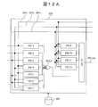
- FIG. 12A is a block diagram showing an internal configuration of the space classifier 222 according to Embodiment 3 of the present invention.
- the space classifier 222 newly includes internal calculation blocks 222_9 to 222_13 in addition to the configuration described in the first embodiment. The difference due to the addition of these will be described below.
- FIG. 12B is a block diagram illustrating details of the internal calculation blocks 222_9 to 222_13.
- the internal calculation block 222_9 receives the normalized difference pixel values 307a to 307c, and individually determines whether they exceed the threshold values in the binarization determination units 222-9a, 222-9b, and 222-9c provided in 222_9. To do. Each threshold value can be different for each detection system. This threshold value is stored in the extraction condition storage unit 250 as a defect extraction parameter. The binarization determination result is sent to the logical sum unit 222-9d. If any of the normalized difference pixel values 307a to 307c is equal to or greater than the threshold value, an output indicating that the pixel is defective is output to the internal calculation block 222_13. Hand over.
- the internal calculation blocks 222_10 and 222_11 perform the same processing as the internal calculation block 222_12.
- the internal calculation block 222_12 will be described.
- 222-12a, 222-12b, and 222-12c are binarization determination units provided in 222-12, and have the same functions as 222-9a, 222-9b, and 222-9c.
- the outputs of 222-12a, 222-12b, and 222-12c are sent to the logical product unit 222-12d, and when all of the normalized difference pixel values 307a to 307c are equal to or larger than the threshold value, it is determined that they are defect candidates. Is delivered to the internal operation block 222_13.
- the threshold values used in 222-12a, 222-12b, and 222-12c can be stored in advance in the extraction condition storage unit 250 and further adjusted as defect extraction parameters.
- the internal calculation blocks 222_10 and 222_11 have the same function as the internal calculation block 222_12, but the threshold values given to the binarization determination unit provided in the internal calculation blocks 222_11 are different from those used in 222-12a, 222-12b, and 222-12c. Set.
- the threshold value can be stored in advance in the extraction condition storage unit 250 and further adjusted as a defect extraction parameter.
- the threshold value applied in the binarization determination units 222-9a, 222-9b, and 222-9c provided in 222_9 is larger than the threshold value used in 222_10, 222_11, and 222_12. Set.
- the internal calculation block 222_13 considers that a pixel determined to be defective by any of the internal calculation blocks 222_10 to 222_12 is a defect candidate. 222_10 to 222_12 are led to a logical sum unit 222_13a provided in 222_13 to take a logical sum. Further, this output is led to the logical product unit 222_13b.
- the internal operation block 222_13 receives the output from the logical sum unit 222_8. 223_13b outputs a pixel that the OR unit 222_8 determines to be a defect candidate and that 222_13a regards as a defect as a defect candidate.
- 222_13c since only the defects that are manifested by both the internal calculation blocks 222_1 to 222_8 and the internal calculation blocks 222_9 to 222_12 can be extracted, it is possible to suppress false information. This result is output to 222_13c.
- the internal calculation block 222_12 is based on the assumption that the pixel is defective when the threshold value is greatly exceeded in any of the detection systems.
- the output of 222_12 is guided to a logical sum unit 222_13c provided in 222_13, and a logical sum with the output of 222_13b is calculated to output a final defect determination output 222_out.
- FIG. 13 is a conceptual diagram showing how the space classifier 222 in Embodiment 3 separates defects and noise.
- FIG. 13 is a conceptual diagram showing how the space classifier 222 in Embodiment 3 separates defects and noise.
- a circle indicates a real report
- a cross indicates a false report
- a triangle indicates an undetected false report.
- the discrimination plane 1301 is a boundary plane that serves as a reference for the internal calculation blocks 222_1 to 222_8 to extract defects using the initial values of the defect extraction parameters.
- a defect candidate placed above the boundary surface is determined as a defect by the space classifier 222. Therefore, the ⁇ mark and the X mark are determined as defects.
- the discrimination surface 1302 is a boundary surface after the defect extraction parameters are adjusted. In this case, a part of the x mark and the ⁇ mark are determined as defects.
- the discrimination plane becomes 1303 by further adjusting the defect extraction parameter, all the defects detected on the discrimination plane 1301 can be detected and all the false information can be eliminated.
- a defect candidate that has not been detected on the determination surface 1301 is also detected as a defect, which may cause erroneous detection.
- FIG. 14 is an example of a setting screen 264 used by the user in the fourth embodiment of the present invention to adjust defect detection parameters.
- the upper half of the screen is the same as the setting screen 262.
- the user inputs to the area label column 2621 that all areas are selected at once.
- the arithmetic device 200 collectively calculates the actual / imaginary number of reports for all area labels in the same procedure as in the first embodiment, and the totaling column 2641 displays the result.
- the tabulated results such as the number of actual reports / number of false reports / number of unclassified labels, actual report rate / false report rate / defect capture rate / defect remaining rate, etc. detected for all area labels are displayed. Any one of these may be selectively displayed.
- the optimization is comprehensively performed for all the areas in Expression 1 and Expression 2.
- automatic adjustment is performed such that the detection sensitivity in a region where defects are likely to occur is increased and the detection sensitivity in a region with many false alarms is decreased. Since the sensitivity index value can be adjusted collectively for all regions, the burden of adjusting the defect extraction parameter can be further suppressed.
- Gi is a coefficient used internally by the space classifier 222, and is an array of coefficients used by each internal calculation block (seven in FIG. 5).
- X is an array of feature quantities, and has the same number of elements as the number of dimensions of the feature quantity space.
- Thi is a detection threshold value.
- Equation 3 can be replaced as the following equation 4.
- j is an index of a defect candidate.
- t (j) is 1 for actual information and -1 for false information.
- class (j) is a classification to which the defect candidate j belongs.
- C () is a cost, and is given to the actual information class when no defect is detected, or to the false information class when a false information is detected.
- ⁇ i is a slack variable.
- J (j) is set to a value of 1 or less if a defect has already been detected when i is other than the current value, and is set to 1 otherwise.
- the present invention is not limited to the above-described embodiments, and includes various modifications.
- the above-described embodiments have been described in detail for easy understanding of the present invention, and are not necessarily limited to those having all the configurations described.
- a part of the configuration of one embodiment can be replaced with the configuration of another embodiment, and the configuration of another embodiment can be added to the configuration of one embodiment.
- the above components, functions, processing units, processing means, etc. may be realized in hardware by designing some or all of them, for example, with an integrated circuit.
- Each of the above-described configurations, functions, and the like may be realized by software by interpreting and executing a program that realizes each function by the processor.
- Information such as programs, tables, and files for realizing each function can be stored in a recording device such as a memory, a hard disk, an SSD (Solid State Drive), or a recording medium such as an IC card, an SD card, or a DVD.
Landscapes
- Engineering & Computer Science (AREA)
- Physics & Mathematics (AREA)
- General Physics & Mathematics (AREA)
- Analytical Chemistry (AREA)
- Biochemistry (AREA)
- Pathology (AREA)
- Immunology (AREA)
- General Health & Medical Sciences (AREA)
- Chemical & Material Sciences (AREA)
- Life Sciences & Earth Sciences (AREA)
- Health & Medical Sciences (AREA)
- Manufacturing & Machinery (AREA)
- General Engineering & Computer Science (AREA)
- Quality & Reliability (AREA)
- Automation & Control Theory (AREA)
- Power Engineering (AREA)
- Microelectronics & Electronic Packaging (AREA)
- Computer Hardware Design (AREA)
- Signal Processing (AREA)
- Computer Vision & Pattern Recognition (AREA)
- Investigating Materials By The Use Of Optical Means Adapted For Particular Applications (AREA)
- Testing Or Measuring Of Semiconductors Or The Like (AREA)
Abstract
Description
図1は、本発明の実施形態1に係る欠陥検査装置100の構成図である。欠陥検査装置100は、試料110の外観画像を撮像し、その外観画像を用いて試料110が有する欠陥を検査する装置である。以下では記載の便宜上、欠陥検査装置100と演算装置200を個別に記載しているが、これらは一体的に構成することもできるし、適当な通信線を介して相互接続することもできる。 <
FIG. 1 is a configuration diagram of a


欠陥検査装置100は、試料110の外観画像を撮像する(S901)。演算装置200は、図3~図5で説明した手順にしたがって、欠陥候補を抽出する(S902)。これを試料110全面の画像が撮像されて欠陥候補が抽出されるまでおこなう(S900)。これらステップにおいては、重要欠陥が検出されるように、虚報数が比較的多い高感度検査を実施することが望ましい。 (FIG. 9: Steps S900 to S902)
The
ユーザは、欠陥候補画面261上で欠陥候補を選択し、各欠陥候補に対して分類を入力する。原則としては各欠陥候補を実報と虚報に分類するが、より詳細な欠陥分類を付与してもよい。ユーザが入力することに代えてまたは併用して、DR-SEM270による判定結果を用いてもよい。演算装置200は、ユーザ入力(例えばキーボードやマウス)またはDR-SEM270との間で判定結果を送受信(例えば通信ネットワーク)するためのインターフェース280を適宜備えることができる。 (FIG. 9: Step S903)
The user selects a defect candidate on the
ユーザは、設定画面262上で複数の感度指標値(または感度指標値の範囲)を入力する(S904)。演算装置200は、ステップS906~S907を、入力された感度指標値ごとに(範囲を指定した場合は等間隔で)実施する(S905)。 (FIG. 9: Steps S904 to S905)
The user inputs a plurality of sensitivity index values (or sensitivity index value ranges) on the setting screen 262 (S904). The
演算装置200は、感度指標値Sを入力パラメータとして、式1(分類を重み付けする場合は式2)にしたがって欠陥検出パラメータを最適化し、これを抽出条件記憶部250内に格納する(S906)。演算装置200は、ステップS906において最適化した欠陥抽出パラメータと各欠陥候補の特徴量とを用いて、実報数/虚報数/未分類数を算出する(S907)。 (FIG. 9: Steps S906 to S907)
The
設定画面262は、グラフ2622内に実報数/虚報数/未分類数を表示する(S908)。ユーザはスライダ2626を用いて感度指標値を選択し、演算装置200はその感度指標値を用いて算出した欠陥抽出パラメータをパラメータテーブル2623と2624に表示する(S909)。ユーザが適用ボタン2627を押下すると、抽出条件記憶部250はその欠陥抽出パラメータを格納し、演算装置200は以後その欠陥抽出パラメータを用いて試料110の欠陥を検査する(S910)。 (FIG. 9: Steps S908 to S910)
The
実施形態1では、感度指標値の範囲を指定することにより各感度指標値に対応する欠陥抽出パラメータを最適化し、ユーザがそのなかから所望する要件を満たすものを選択する構成例を説明した。本発明の実施形態2では、感度指標値以外のパラメータを用いて同様の処理を実施する構成例を説明する。その他構成は実施形態1と同様であるため、以下では主に感度指標値に代えて用いるパラメータについて説明する。 <
In the first embodiment, the configuration example has been described in which the defect extraction parameter corresponding to each sensitivity index value is optimized by specifying the range of the sensitivity index value, and the one that satisfies the requirement desired by the user is selected. In the second embodiment of the present invention, a configuration example in which similar processing is performed using parameters other than sensitivity index values will be described. Since the other configuration is the same as that of the first embodiment, parameters used in place of the sensitivity index value will be mainly described below.
ユーザは、設定画面263上でいずれのパラメータを基準として欠陥抽出パラメータを最適化するかを選択するとともに、その値範囲(または複数の値)を入力する(S1101)。演算装置200は、ステップS906~S907を、入力された基準パラメータごとに(範囲を指定した場合は等間隔で)実施する(S1102)。 (FIG. 11: Step S1101)
On the
演算装置200は、ユーザがパラメータテーブル2632上で選択した欠陥抽出パラメータの詳細を、パラメータテーブル2633と2634に表示する。 (FIG. 11: Step S1103)
The
図12Aは、本発明の実施形態3における空間分類器222の内部構成を示すブロック図である。本実施形態3において空間分類器222は、実施形態1で説明した構成に加えて新たに内部演算ブロック222_9~222_13を備える。以下これらを追加したことにともなう差異点について説明する。 <
FIG. 12A is a block diagram showing an internal configuration of the
図14は、本発明の実施形態4においてユーザが欠陥検出パラメータを調整するために用いる設定画面264の例である。画面の上半分は設定画面262と同様である。ただしユーザは領域ラベル欄2621に対して全領域を一括して選択する旨を入力する。演算装置200は、全領域ラベルについて一括して実施形態1と同様の手順により実報数/虚報数などを算出し、集計欄2641はその結果を表示する。具体的には、全領域ラベルについて検出した実報数/虚報数/未分類数、実報率/虚報率/欠陥捕捉率/欠陥残存率などの集計結果を表示する。これらのうちいずれかを選択的に表示してもよい。 <
FIG. 14 is an example of a
本発明の実施形態5では、演算装置200が欠陥を検出するために用いる具体的な演算式について説明する。欠陥検査装置100および演算装置200の構成は実施形態1~4と同様である。 <
In the fifth embodiment of the present invention, a specific arithmetic expression used for the


本発明は上記した実施例に限定されるものではなく、様々な変形例が含まれる。例えば、上記した実施例は本発明を分かりやすく説明するために詳細に説明したものであり、必ずしも説明した全ての構成を備えるものに限定されるものではない。また、ある実施例の構成の一部を他の実施例の構成に置き換えることが可能であり、また、ある実施例の構成に他の実施例の構成を加えることも可能である。また、各実施例の構成の一部について、他の構成の追加・削除・置換をすることが可能である。 <Modification of the present invention>
The present invention is not limited to the above-described embodiments, and includes various modifications. For example, the above-described embodiments have been described in detail for easy understanding of the present invention, and are not necessarily limited to those having all the configurations described. Further, a part of the configuration of one embodiment can be replaced with the configuration of another embodiment, and the configuration of another embodiment can be added to the configuration of one embodiment. Further, it is possible to add, delete, and replace other configurations for a part of the configuration of each embodiment.
Claims (15)
- 検査対象が有する欠陥を検査する欠陥検査装置であって、
前記検査対象の外観画像を生成する画像生成部、
前記外観画像の特徴量を算出する特徴量算出部、
前記検査対象の欠陥を抽出する条件の初期値を記述した抽出条件データを格納する記憶部、
前記特徴量と前記条件とを比較することにより前記検査対象が有する欠陥を抽出する欠陥判定部、
前記欠陥判定部が抽出した欠陥を表す情報を出力する出力部、
前記欠陥判定部が抽出した欠陥が実報と虚報のいずれであるかを指定する指定入力を受け取るインターフェース、
を備え、
前記欠陥判定部は、前記インターフェースを介して複数の基準値を受け取るとともに、実報数と虚報数と前記基準値を用いて算出される評価値が最適になる前記条件を、前記基準値ごとに算出し、
前記欠陥判定部は、前記基準値ごとに算出した前記条件を用いて前記検査対象が有する欠陥を抽出し、
前記出力部は、前記欠陥判定部が前記基準値ごとに算出した前記条件を前記基準値ごとにそれぞれ出力するとともに、前記欠陥判定部が前記基準値ごとに算出した前記条件を用いて抽出した欠陥を表す情報を出力する
ことを特徴とする欠陥検査装置。 A defect inspection apparatus for inspecting a defect of an inspection object,
An image generating unit for generating an appearance image of the inspection target;
A feature amount calculation unit for calculating a feature amount of the appearance image;
A storage unit for storing extraction condition data describing initial values of conditions for extracting the defect to be inspected;
A defect determination unit that extracts defects of the inspection object by comparing the feature amount and the condition;
An output unit that outputs information representing the defect extracted by the defect determination unit;
An interface for receiving a designation input for designating whether the defect extracted by the defect determination unit is a real report or a false report;
With
The defect determination unit receives a plurality of reference values via the interface, and sets the condition that the evaluation value calculated using the actual report number, the false report number, and the reference value is optimal for each reference value. Calculate
The defect determination unit extracts defects that the inspection target has using the condition calculated for each reference value,
The output unit outputs the condition calculated for each reference value by the defect determination unit for each reference value, and the defect extracted using the condition calculated by the defect determination unit for each reference value. A defect inspection apparatus characterized by outputting information representing - 前記欠陥判定部は、前記実報数と前記虚報数の合計に対する前記実報数の比率を表す実報率を算出し、前記実報率を用いて前記評価値を算出することにより、前記条件として前記実報率を用いて欠陥を抽出する
ことを特徴とする請求項1記載の欠陥検査装置。 The defect determination unit calculates an actual report rate that represents a ratio of the actual report number to the total of the actual report number and the false report number, and calculates the evaluation value using the actual report rate, thereby calculating the condition. The defect inspection apparatus according to claim 1, wherein a defect is extracted using the actual report rate. - 前記欠陥判定部は、前記基準値として、前記評価値における前記実報率の重みを指定する数値を受け取り、その重みを用いて前記評価値を算出する
ことを特徴とする請求項2記載の欠陥検査装置。 The defect according to claim 2, wherein the defect determination unit receives a numerical value designating a weight of the actual report rate in the evaluation value as the reference value, and calculates the evaluation value using the weight. Inspection device. - 前記欠陥判定部は、前記検査対象が有する欠陥を前記特徴量にしたがって分類するとともに、前記欠陥の分類ごとに重み係数をセットし、
前記欠陥判定部は、前記分類のうち前記実報に属するものについては、前記重み係数が大きいほど前記評価値が高くなるように前記重み係数を設定するとともに、前記分類のうち前記虚報に属するものについては、前記重み係数が大きいほど前記評価値が低くなるように前記重み係数を設定する
ことを特徴とする請求項1記載の欠陥検査装置。 The defect determination unit classifies the defect that the inspection target has according to the feature amount, sets a weighting factor for each classification of the defect,
The defect determination unit sets the weighting factor so that the evaluation value is higher as the weighting factor is larger for the classification belonging to the actual report, and the defect determination unit belongs to the false reporting among the classifications The defect inspection apparatus according to claim 1, wherein the weighting factor is set so that the evaluation value decreases as the weighting factor increases. - 前記欠陥判定部は、前記基準値として、前記条件の初期値を用いて検出した前記実報数に対する前記実報数の比率を表す欠陥捕捉率の数値を受け取り、
前記欠陥判定部は、前記欠陥捕捉率を用いて前記評価値を算出することにより、前記条件として前記欠陥捕捉率を用いて欠陥を抽出する
ことを特徴とする請求項1記載の欠陥検査装置。 The defect determination unit receives a numerical value of a defect capture rate representing a ratio of the actual number of reports to the actual number of reports detected using the initial value of the condition as the reference value,
The defect inspection apparatus according to claim 1, wherein the defect determination unit extracts defects using the defect capture rate as the condition by calculating the evaluation value using the defect capture rate. - 前記欠陥判定部は、前記基準値として、前記実報数と前記虚報数の合計に対する前記虚報数の比率を表す虚報率の数値を受け取り、
前記欠陥判定部は、前記虚報率を用いて前記評価値を算出することにより、前記条件として前記虚報率を用いて欠陥を抽出する
ことを特徴とする請求項1記載の欠陥検査装置。 The defect determination unit receives a numerical value of a false alarm rate representing a ratio of the false alarm number to the total of the actual alarm number and the false alarm number as the reference value,
The defect inspection apparatus according to claim 1, wherein the defect determination unit extracts the defect using the false information rate as the condition by calculating the evaluation value using the false information rate. - 前記欠陥判定部は、前記基準値として、前記条件の初期値を用いて検出した前記虚報数に対する前記虚報数の比率を表す欠陥残存率の数値を受け取り、
前記欠陥判定部は、前記欠陥残存率を用いて前記評価値を算出することにより、前記条件として前記欠陥残存率を用いて欠陥を抽出する
ことを特徴とする請求項1記載の欠陥検査装置。 The defect determination unit receives a numerical value of a defect remaining rate representing a ratio of the number of false reports to the number of false reports detected using the initial value of the condition as the reference value,
The defect inspection apparatus according to claim 1, wherein the defect determination unit extracts the defect using the defect remaining rate as the condition by calculating the evaluation value using the defect remaining rate. - 前記欠陥検査装置は、前記検査対象を撮像することにより前記外観画像の画素値を取得して前記画像生成部に対して引き渡す検出系を複数備え、
前記欠陥検査装置はさらに、前記検出系が取得した前記外観画像の画素値と参照画像の画素値との間の差分を前記検出系ごとに算出する差分算出器を備え、
前記欠陥判定部は、1以上の前記検出系について前記差分算出器がそれぞれ算出した前記差分の線形和を求め、前記線形和が第1判定閾値を超えている場合は、前記差分に対応する画素が欠陥であると判定する
ことを特徴とする請求項1記載の欠陥検査装置。 The defect inspection apparatus includes a plurality of detection systems that acquire the pixel value of the appearance image by imaging the inspection object and deliver the pixel value to the image generation unit,
The defect inspection apparatus further includes a difference calculator that calculates a difference between a pixel value of the appearance image acquired by the detection system and a pixel value of a reference image for each detection system,
The defect determination unit obtains a linear sum of the differences respectively calculated by the difference calculator for one or more of the detection systems, and when the linear sum exceeds a first determination threshold, a pixel corresponding to the difference The defect inspection apparatus according to claim 1, wherein the defect inspection apparatus determines that the defect is a defect. - 前記欠陥検査装置は、前記検査対象を撮像することにより前記外観画像の画素値を取得して前記画像生成部に対して引き渡す検出系を複数備え、
前記欠陥検査装置はさらに、前記検出系が取得した前記外観画像の画素値と参照画像の画素値との間の差分を前記検出系ごとに算出する差分算出器を備え、
前記欠陥判定部は、前記検出系ごとに同一または異なる第2判定閾値をあらかじめセットし、前記差分が全ての前記検出系について前記第2判定閾値を超えている場合は、前記差分に対応する画素が欠陥であると判定する
ことを特徴とする請求項1記載の欠陥検査装置。 The defect inspection apparatus includes a plurality of detection systems that acquire the pixel value of the appearance image by imaging the inspection object and deliver the pixel value to the image generation unit,
The defect inspection apparatus further includes a difference calculator that calculates a difference between a pixel value of the appearance image acquired by the detection system and a pixel value of a reference image for each detection system,
The defect determination unit sets in advance a second determination threshold that is the same or different for each detection system, and when the difference exceeds the second determination threshold for all the detection systems, a pixel corresponding to the difference The defect inspection apparatus according to claim 1, wherein the defect inspection apparatus determines that the defect is a defect. - 前記欠陥判定部は、前記検出系ごとに同一または異なる第2判定閾値をあらかじめセットし、
前記欠陥判定部は、前記線形和が前記第1判定閾値を超えており、かつ前記差分が全ての前記検出系について前記第2判定閾値を超えている場合は、前記差分に対応する画素が欠陥であると判定する
ことを特徴とする請求項8記載の欠陥検査装置。 The defect determination unit sets in advance a second determination threshold that is the same or different for each detection system,
When the linear sum exceeds the first determination threshold and the difference exceeds the second determination threshold for all the detection systems, the defect determination unit determines that a pixel corresponding to the difference is defective. The defect inspection apparatus according to claim 8, wherein the defect inspection apparatus is determined to be. - 前記画像生成部は、前記検査対象の部分領域について前記外観画像を生成するとともに前記部分領域の識別子を前記外観画像に対して付与し、
前記欠陥判定部は、前記検査対象が有する欠陥を前記部分領域ごとに抽出する
ことを特徴とする請求項1記載の欠陥検査装置。 The image generation unit generates the appearance image for the partial area to be inspected and gives an identifier of the partial area to the appearance image.
The defect inspection apparatus according to claim 1, wherein the defect determination unit extracts a defect included in the inspection target for each partial region. - 前記画像生成部は、前記検査対象の部分領域について前記外観画像を生成するとともに前記部分領域の識別子を前記外観画像に対して付与し、
前記欠陥判定部は、前記検査対象が有する欠陥を全ての前記部分領域について一括して抽出するとともに、全ての前記部分領域についての前記実報数と前記虚報数を用いて前記評価値を算出することにより、全ての前記部分領域の総和に対して前記評価値を最適化する
ことを特徴とする請求項1記載の欠陥検査装置。 The image generation unit generates the appearance image for the partial area to be inspected and gives an identifier of the partial area to the appearance image.
The defect determination unit collectively extracts defects of the inspection target for all the partial areas, and calculates the evaluation value using the actual report numbers and the false report numbers for all the partial areas. The defect inspection apparatus according to claim 1, wherein the evaluation value is optimized with respect to a sum of all the partial areas. - 前記欠陥検査装置は、
複数の前記検査対象の外観画像を合成することにより参照画像を生成する参照画像生成部、
前記外観画像の画素値と前記参照画像の画素値との間の差分を算出する差分算出部、
前記検査対象が有する欠陥を前記特徴量にしたがって分類するクラスタリング部、
前記差分算出部が算出した差分と前記クラスタリング部による分類結果とを用いて前記外観画像の画素値のばらつきを算出するノイズ推定部、
前記ノイズ推定部が算出したばらつきを前記差分算出部が算出した差分によって正規化するとともに前記正規化によって得られた画素値と第1閾値とを比較することにより欠陥候補を抽出する正規化器、
前記欠陥候補の特徴量を算出する正規化特徴量算出器、
前記正規化特徴量算出器が算出した特徴量と第2閾値とを比較することにより前記正規化器が抽出した欠陥候補からさらに最終的な欠陥候補を抽出する判定器、
を備えることを特徴とする請求項1記載の欠陥検査装置。 The defect inspection apparatus includes:
A reference image generation unit that generates a reference image by combining a plurality of appearance images of the inspection target;
A difference calculating unit that calculates a difference between a pixel value of the appearance image and a pixel value of the reference image;
A clustering unit that classifies the defects of the inspection target according to the feature amount;
A noise estimation unit that calculates variations in pixel values of the appearance image using the difference calculated by the difference calculation unit and the classification result by the clustering unit;
A normalizer for extracting defect candidates by normalizing the variation calculated by the noise estimation unit with the difference calculated by the difference calculation unit and comparing the pixel value obtained by the normalization with a first threshold value,
A normalized feature amount calculator for calculating the feature amount of the defect candidate;
A determinator for further extracting a final defect candidate from the defect candidates extracted by the normalizer by comparing the feature amount calculated by the normalized feature amount calculator with a second threshold;
The defect inspection apparatus according to claim 1, further comprising: - 前記欠陥判定部は、前記基準値ごとに算出した前記条件のうちいずれを用いるかを指定する指示を受け取り、その条件を用いて前記検査対象が有する欠陥を抽出する
ことを特徴とする請求項1記載の欠陥検査装置。 The defect determination unit receives an instruction that specifies which of the conditions calculated for each of the reference values is used, and extracts a defect included in the inspection target using the condition. Defect inspection apparatus as described. - 検査対象が有する欠陥を検査する欠陥検査方法であって、
前記検査対象の外観画像を生成する画像生成ステップ、
前記外観画像の特徴量を算出する特徴量算出ステップ、
前記検査対象の欠陥を抽出する条件の初期値を記述した検出条件データを記憶部から読み取るステップ、
前記特徴量と前記条件とを比較することにより前記検査対象が有する欠陥を抽出する欠陥判定ステップ、
前記欠陥判定ステップにおいて抽出した欠陥を表す情報を出力する出力ステップ、
前記欠陥判定ステップにおいて抽出した欠陥が実報と虚報のいずれであるかを指定する指定入力を受け取るステップ、
を有し、
前記欠陥判定ステップにおいてはさらに、複数の基準値を受け取るとともに、実報数と虚報数と前記基準値を用いて算出される評価値が最適になる前記条件を、前記基準値ごとに算出し、
前記欠陥判定ステップにおいてはさらに、前記基準値ごとに算出した前記条件を用いて前記検査対象が有する欠陥を抽出し、
前記出力ステップにおいてはさらに、前記欠陥判定ステップにおいて前記基準値ごとに算出した前記条件を出力するとともに、前記欠陥判定ステップにおいて前記基準値ごとに算出した前記条件を用いて抽出した欠陥を表す情報を出力する
ことを特徴とする欠陥検査方法。 A defect inspection method for inspecting defects possessed by an inspection object,
An image generation step of generating an appearance image of the inspection object;
A feature amount calculating step for calculating a feature amount of the appearance image;
Reading detection condition data describing initial values of conditions for extracting the defect to be inspected from the storage unit;
A defect determination step of extracting defects of the inspection object by comparing the feature amount and the condition;
An output step of outputting information representing the defect extracted in the defect determination step;
Receiving a designation input designating whether the defect extracted in the defect determination step is a real report or a false report;
Have
In the defect determination step, a plurality of reference values are received, and the conditions under which the evaluation value calculated using the number of actual reports, the number of false reports, and the reference values are optimized are calculated for each of the reference values,
In the defect determination step, further, the defect of the inspection object is extracted using the condition calculated for each reference value,
In the output step, the condition calculated for each reference value in the defect determination step is output, and information representing a defect extracted using the condition calculated for each reference value in the defect determination step A defect inspection method characterized by output.
Priority Applications (4)
| Application Number | Priority Date | Filing Date | Title |
|---|---|---|---|
| US16/085,890 US10466181B2 (en) | 2016-03-30 | 2016-03-30 | Flaw inspection device and flaw inspection method |
| KR1020187022692A KR102084535B1 (en) | 2016-03-30 | 2016-03-30 | Defect inspection device, defect inspection method |
| PCT/JP2016/060375 WO2017168630A1 (en) | 2016-03-30 | 2016-03-30 | Flaw inspection device and flaw inspection method |
| US16/661,305 US10816484B2 (en) | 2016-03-30 | 2019-10-23 | Flaw inspection device and flaw inspection method |
Applications Claiming Priority (1)
| Application Number | Priority Date | Filing Date | Title |
|---|---|---|---|
| PCT/JP2016/060375 WO2017168630A1 (en) | 2016-03-30 | 2016-03-30 | Flaw inspection device and flaw inspection method |
Related Child Applications (2)
| Application Number | Title | Priority Date | Filing Date |
|---|---|---|---|
| US16/085,890 A-371-Of-International US10466181B2 (en) | 2016-03-30 | 2016-03-30 | Flaw inspection device and flaw inspection method |
| US16/661,305 Continuation US10816484B2 (en) | 2016-03-30 | 2019-10-23 | Flaw inspection device and flaw inspection method |
Publications (1)
| Publication Number | Publication Date |
|---|---|
| WO2017168630A1 true WO2017168630A1 (en) | 2017-10-05 |
Family
ID=59962761
Family Applications (1)
| Application Number | Title | Priority Date | Filing Date |
|---|---|---|---|
| PCT/JP2016/060375 WO2017168630A1 (en) | 2016-03-30 | 2016-03-30 | Flaw inspection device and flaw inspection method |
Country Status (3)
| Country | Link |
|---|---|
| US (2) | US10466181B2 (en) |
| KR (1) | KR102084535B1 (en) |
| WO (1) | WO2017168630A1 (en) |
Cited By (3)
| Publication number | Priority date | Publication date | Assignee | Title |
|---|---|---|---|---|
| EP3961332A1 (en) * | 2016-11-14 | 2022-03-02 | Koh Young Technology Inc. | Method and device for adjusting quality determination conditions for test body |
| US11366068B2 (en) | 2016-11-14 | 2022-06-21 | Koh Young Technology Inc. | Inspection apparatus and operating method thereof |
| JP7416071B2 (en) | 2019-08-23 | 2024-01-17 | コニカミノルタ株式会社 | Judgment device and judgment program |
Families Citing this family (7)
| Publication number | Priority date | Publication date | Assignee | Title |
|---|---|---|---|---|
| US11047806B2 (en) * | 2016-11-30 | 2021-06-29 | Kla-Tencor Corporation | Defect discovery and recipe optimization for inspection of three-dimensional semiconductor structures |
| US11237119B2 (en) * | 2017-01-10 | 2022-02-01 | Kla-Tencor Corporation | Diagnostic methods for the classifiers and the defects captured by optical tools |
| WO2018216629A1 (en) * | 2017-05-22 | 2018-11-29 | キヤノン株式会社 | Information processing device, information processing method, and program |
| US10460434B2 (en) * | 2017-08-22 | 2019-10-29 | Applied Materials Israel Ltd. | Method of defect detection and system thereof |
| US10902582B2 (en) * | 2019-01-17 | 2021-01-26 | Applied Materials Israel, Ltd. | Computerized system and method for obtaining information about a region of an object |
| JP7316850B2 (en) * | 2019-06-21 | 2023-07-28 | 東京エレクトロン株式会社 | Processing system and processing method |
| CN113888772B (en) * | 2021-09-30 | 2024-04-26 | 江苏欧软信息科技有限公司 | MES-based information input emergency system and processing method thereof |
Citations (4)
| Publication number | Priority date | Publication date | Assignee | Title |
|---|---|---|---|---|
| JP2004177139A (en) * | 2002-11-25 | 2004-06-24 | Renesas Technology Corp | Support program for preparation of inspection condition data, inspection device, and method of preparing inspection condition data |
| JP2004239728A (en) * | 2003-02-05 | 2004-08-26 | Hitachi High-Technologies Corp | Pattern inspection method and device |
| JP2005017159A (en) * | 2003-06-27 | 2005-01-20 | Hitachi High-Technologies Corp | Inspection recipe setting method in flaw inspection device and flaw inspecting method |
| JP2013224942A (en) * | 2012-04-19 | 2013-10-31 | Applied Materials Israel Ltd | Optimization of unknown defect rejection for automatic defect classification |
Family Cites Families (8)
| Publication number | Priority date | Publication date | Assignee | Title |
|---|---|---|---|---|
| GB2417090A (en) * | 2003-04-28 | 2006-02-15 | Stephen James Crampton | CMM arm with exoskeleton |
| US6985220B1 (en) | 2003-08-20 | 2006-01-10 | Kla-Tencor Technologies Corporation | Interactive threshold tuning |
| GB0508395D0 (en) * | 2005-04-26 | 2005-06-01 | Renishaw Plc | Method for scanning the surface of a workpiece |
| EP2977719A1 (en) * | 2007-08-17 | 2016-01-27 | Renishaw plc | Non-contact measurement apparatus and method |
| GB0716218D0 (en) * | 2007-08-20 | 2007-09-26 | Renishaw Plc | Measurement path generation |
| GB0909635D0 (en) * | 2009-06-04 | 2009-07-22 | Renishaw Plc | Vision measurement probe |
| JP5537282B2 (en) * | 2009-09-28 | 2014-07-02 | 株式会社日立ハイテクノロジーズ | Defect inspection apparatus and defect inspection method |
| JP5433631B2 (en) * | 2011-05-20 | 2014-03-05 | 株式会社日立ハイテクノロジーズ | Defect inspection method and system for semiconductor device |
-
2016
- 2016-03-30 KR KR1020187022692A patent/KR102084535B1/en active IP Right Grant
- 2016-03-30 US US16/085,890 patent/US10466181B2/en active Active
- 2016-03-30 WO PCT/JP2016/060375 patent/WO2017168630A1/en active Application Filing
-
2019
- 2019-10-23 US US16/661,305 patent/US10816484B2/en active Active
Patent Citations (4)
| Publication number | Priority date | Publication date | Assignee | Title |
|---|---|---|---|---|
| JP2004177139A (en) * | 2002-11-25 | 2004-06-24 | Renesas Technology Corp | Support program for preparation of inspection condition data, inspection device, and method of preparing inspection condition data |
| JP2004239728A (en) * | 2003-02-05 | 2004-08-26 | Hitachi High-Technologies Corp | Pattern inspection method and device |
| JP2005017159A (en) * | 2003-06-27 | 2005-01-20 | Hitachi High-Technologies Corp | Inspection recipe setting method in flaw inspection device and flaw inspecting method |
| JP2013224942A (en) * | 2012-04-19 | 2013-10-31 | Applied Materials Israel Ltd | Optimization of unknown defect rejection for automatic defect classification |
Cited By (3)
| Publication number | Priority date | Publication date | Assignee | Title |
|---|---|---|---|---|
| EP3961332A1 (en) * | 2016-11-14 | 2022-03-02 | Koh Young Technology Inc. | Method and device for adjusting quality determination conditions for test body |
| US11366068B2 (en) | 2016-11-14 | 2022-06-21 | Koh Young Technology Inc. | Inspection apparatus and operating method thereof |
| JP7416071B2 (en) | 2019-08-23 | 2024-01-17 | コニカミノルタ株式会社 | Judgment device and judgment program |
Also Published As
| Publication number | Publication date |
|---|---|
| US10816484B2 (en) | 2020-10-27 |
| US10466181B2 (en) | 2019-11-05 |
| US20200057003A1 (en) | 2020-02-20 |
| US20190094155A1 (en) | 2019-03-28 |
| KR102084535B1 (en) | 2020-03-05 |
| KR20180102117A (en) | 2018-09-14 |
Similar Documents
| Publication | Publication Date | Title |
|---|---|---|
| WO2017168630A1 (en) | Flaw inspection device and flaw inspection method | |
| WO2018061067A1 (en) | Defect inspection device and defect inspection method | |
| JP7200113B2 (en) | Systems and methods for training and applying defect classifiers on wafers with deeply stacked layers | |
| KR102307415B1 (en) | Virtual inspection systems with multiple modes | |
| KR102079418B1 (en) | Detecting defects on a wafer | |
| US9607233B2 (en) | Classifier readiness and maintenance in automatic defect classification | |
| KR102276921B1 (en) | Defect detection using structural information | |
| TW202029071A (en) | System and method for determining type and size of defects on blank reticles | |
| US9262821B2 (en) | Inspection recipe setup from reference image variation | |
| US20130094750A1 (en) | Methods and systems for segmentation of cells for an automated differential counting system | |
| US20130202188A1 (en) | Defect inspection method, defect inspection apparatus, program product and output unit | |
| CN112840205B (en) | Design and noise based regions of interest | |
| TW201511157A (en) | Methods and systems for detecting repeating defects on semiconductor wafers using design data | |
| KR20220014805A (en) | Generating training data usable for examination of a semiconductor specimen | |
| US10670536B2 (en) | Mode selection for inspection | |
| JP2019061484A (en) | Image processing device and control method thereof and program | |
| Marée | The need for careful data collection for pattern recognition in digital pathology | |
| US20220138939A1 (en) | Systems and Methods for Digital Pathology | |
| TWI785270B (en) | Detecting defects in a logic region on a wafer | |
| JP2013033017A (en) | Surface inspection device, surface inspection method, surface inspection program, and computer-readable recording medium | |
| KR20220066168A (en) | How to extract the spectral information of the material to be measured | |
| JP5530126B2 (en) | Three-dimensional cell image analysis system and three-dimensional cell image analyzer used therefor | |
| JP2023145412A (en) | Defect detection method and system | |
| CN110441315A (en) | Electronic component test equipment and method | |
| KR20150060771A (en) | Automatic morphometry and classification of crystals of iron oxides |
Legal Events
| Date | Code | Title | Description |
|---|---|---|---|
| ENP | Entry into the national phase |
Ref document number: 20187022692 Country of ref document: KR Kind code of ref document: A |
|
| WWE | Wipo information: entry into national phase |
Ref document number: 1020187022692 Country of ref document: KR |
|
| NENP | Non-entry into the national phase |
Ref country code: DE |
|
| 121 | Ep: the epo has been informed by wipo that ep was designated in this application |
Ref document number: 16896849 Country of ref document: EP Kind code of ref document: A1 |
|
| 122 | Ep: pct application non-entry in european phase |
Ref document number: 16896849 Country of ref document: EP Kind code of ref document: A1 |
|
| NENP | Non-entry into the national phase |
Ref country code: JP |