WO2017163034A1 - Heterostructure - Google Patents
Heterostructure Download PDFInfo
- Publication number
- WO2017163034A1 WO2017163034A1 PCT/GB2017/050769 GB2017050769W WO2017163034A1 WO 2017163034 A1 WO2017163034 A1 WO 2017163034A1 GB 2017050769 W GB2017050769 W GB 2017050769W WO 2017163034 A1 WO2017163034 A1 WO 2017163034A1
- Authority
- WO
- WIPO (PCT)
- Prior art keywords
- layer
- dislocation
- strain
- thickness product
- heterostructure
- Prior art date
- Legal status (The legal status is an assumption and is not a legal conclusion. Google has not performed a legal analysis and makes no representation as to the accuracy of the status listed.)
- Ceased
Links
Classifications
-
- H—ELECTRICITY
- H10—SEMICONDUCTOR DEVICES; ELECTRIC SOLID-STATE DEVICES NOT OTHERWISE PROVIDED FOR
- H10P—GENERIC PROCESSES OR APPARATUS FOR THE MANUFACTURE OR TREATMENT OF DEVICES COVERED BY CLASS H10
- H10P14/00—Formation of materials, e.g. in the shape of layers or pillars
- H10P14/20—Formation of materials, e.g. in the shape of layers or pillars of semiconductor materials
- H10P14/29—Formation of materials, e.g. in the shape of layers or pillars of semiconductor materials characterised by the substrates
- H10P14/2901—Materials
- H10P14/2902—Materials being Group IVA materials
- H10P14/2905—Silicon, silicon germanium or germanium
-
- H—ELECTRICITY
- H10—SEMICONDUCTOR DEVICES; ELECTRIC SOLID-STATE DEVICES NOT OTHERWISE PROVIDED FOR
- H10P—GENERIC PROCESSES OR APPARATUS FOR THE MANUFACTURE OR TREATMENT OF DEVICES COVERED BY CLASS H10
- H10P14/00—Formation of materials, e.g. in the shape of layers or pillars
- H10P14/20—Formation of materials, e.g. in the shape of layers or pillars of semiconductor materials
- H10P14/32—Formation of materials, e.g. in the shape of layers or pillars of semiconductor materials characterised by intermediate layers between substrates and deposited layers
- H10P14/3202—Materials thereof
- H10P14/3214—Materials thereof being Group IIIA-VA semiconductors
- H10P14/3221—Arsenides
-
- H—ELECTRICITY
- H10—SEMICONDUCTOR DEVICES; ELECTRIC SOLID-STATE DEVICES NOT OTHERWISE PROVIDED FOR
- H10P—GENERIC PROCESSES OR APPARATUS FOR THE MANUFACTURE OR TREATMENT OF DEVICES COVERED BY CLASS H10
- H10P14/00—Formation of materials, e.g. in the shape of layers or pillars
- H10P14/20—Formation of materials, e.g. in the shape of layers or pillars of semiconductor materials
- H10P14/32—Formation of materials, e.g. in the shape of layers or pillars of semiconductor materials characterised by intermediate layers between substrates and deposited layers
- H10P14/3242—Structure
- H10P14/3244—Layer structure
- H10P14/3251—Layer structure consisting of three or more layers
-
- H—ELECTRICITY
- H10—SEMICONDUCTOR DEVICES; ELECTRIC SOLID-STATE DEVICES NOT OTHERWISE PROVIDED FOR
- H10P—GENERIC PROCESSES OR APPARATUS FOR THE MANUFACTURE OR TREATMENT OF DEVICES COVERED BY CLASS H10
- H10P14/00—Formation of materials, e.g. in the shape of layers or pillars
- H10P14/20—Formation of materials, e.g. in the shape of layers or pillars of semiconductor materials
- H10P14/32—Formation of materials, e.g. in the shape of layers or pillars of semiconductor materials characterised by intermediate layers between substrates and deposited layers
- H10P14/3242—Structure
- H10P14/3244—Layer structure
- H10P14/3251—Layer structure consisting of three or more layers
- H10P14/3252—Alternating layers, e.g. superlattice
-
- H—ELECTRICITY
- H10—SEMICONDUCTOR DEVICES; ELECTRIC SOLID-STATE DEVICES NOT OTHERWISE PROVIDED FOR
- H10P—GENERIC PROCESSES OR APPARATUS FOR THE MANUFACTURE OR TREATMENT OF DEVICES COVERED BY CLASS H10
- H10P14/00—Formation of materials, e.g. in the shape of layers or pillars
- H10P14/20—Formation of materials, e.g. in the shape of layers or pillars of semiconductor materials
- H10P14/34—Deposited materials, e.g. layers
- H10P14/3402—Deposited materials, e.g. layers characterised by the chemical composition
- H10P14/3414—Deposited materials, e.g. layers characterised by the chemical composition being group IIIA-VIA materials
- H10P14/3421—Arsenides
-
- H—ELECTRICITY
- H10—SEMICONDUCTOR DEVICES; ELECTRIC SOLID-STATE DEVICES NOT OTHERWISE PROVIDED FOR
- H10P—GENERIC PROCESSES OR APPARATUS FOR THE MANUFACTURE OR TREATMENT OF DEVICES COVERED BY CLASS H10
- H10P95/00—Generic processes or apparatus for manufacture or treatments not covered by the other groups of this subclass
- H10P95/90—Thermal treatments, e.g. annealing or sintering
-
- Y—GENERAL TAGGING OF NEW TECHNOLOGICAL DEVELOPMENTS; GENERAL TAGGING OF CROSS-SECTIONAL TECHNOLOGIES SPANNING OVER SEVERAL SECTIONS OF THE IPC; TECHNICAL SUBJECTS COVERED BY FORMER USPC CROSS-REFERENCE ART COLLECTIONS [XRACs] AND DIGESTS
- Y10—TECHNICAL SUBJECTS COVERED BY FORMER USPC
- Y10S—TECHNICAL SUBJECTS COVERED BY FORMER USPC CROSS-REFERENCE ART COLLECTIONS [XRACs] AND DIGESTS
- Y10S438/00—Semiconductor device manufacturing: process
- Y10S438/938—Lattice strain control or utilization
Definitions
- the present invention relates to a heterostructure comprising a dislocation filter layer structure.
- the present invention seeks to provide an improved heterostructure for reducing density of threading dislocation density, pro, particularly for materials with a high (> 4%) lattice mismatch.
- a method of growing a heterostructure comprises growing an epitaxial multilayer structure on a base structure, the multilayer structure comprising a dislocation filter layer structure comprising a stack of at least two dislocation filter layers and a device layer structure disposed on the dislocation filter structure comprising at least one layer.
- the method comprises providing at least one layer in the dislocation filter layer structure for inhibiting movement of threading dislocations.
- the threading dislocation movement inhibiting layer is interposed between two dislocation filter layers.
- the method comprises relaxing each layer in the dislocation filter layer structure before growing a subsequent layer such that, for each layer in the dislocation filter layer structure which is grown on a respective underlying layer (a) misfit strain-thickness product Boh is equal to or greater than the equilibrium strain-thickness product ⁇ h c when the underlying layer is relaxed and (b) strain-thickness product ⁇ h is equal to or less than the critical strain-thickness product ( ⁇ h)* for dislocation multiplication during growth.
- an improved heterostructure can be grown in which the device layer structure can have a low density of threading dislocations.
- the multilayer structure may further comprise a device layer structure disposed on the dislocation filter structure, the device layer comprising at least one layer, and the method may comprise relaxing each layer in the device layer structure before growing a subsequent layer such that, for each layer in the device layer structure which is grown on a respective underlying layer (a) misfit strain-thickness product eji is equal to or greater than the equilibrium strain-thickness product ⁇ hc when the underlying layer is relaxed and (b) strain-thickness product ⁇ h is equal to or less than the critical strain- thickness product ( ⁇ h)* for dislocation multiplication during growth.
- a method of growing a heterostructure comprises growing a device layer structure comprising at least one layer on a dislocation filter layer structure comprising a stack of at least two dislocation filter layers and at least one layer for inhibiting movement of threading dislocations, wherein the threading dislocation movement inhibiting layer is interposed between two dislocation filter layers.
- the method comprises relaxing each layer in the device layer structure before growing a subsequent layer such that, for each layer in the device layer structure which is grown on a respective underlying layer (a) misfit strain-thickness product ⁇ o h is equal to or greater than the equilibrium strain- thickness product she when the underlying layer is relaxed and (b) strain-thickness product eh is equal to or less than the critical strain-thickness product (eh)* for dislocation multiplication during growth.
- Relaxing a layer may comprise growing a layer sufficiently slowly that relaxation takes place in-situ. Relaxing a layer may comprise pausing growth, waiting and resuming growth of the layer. Relaxing a layer may comprise growing the layer, then waiting until the layer has relaxed. The waiting period maybe chosen dependent on dislocation velocity. Relaxing a layer may comprise annealing. The anneal temperature may chosen such that the time required to anneal the layer is less than 100 minutes, less than 50 minutes or less than 20 minutes. The waiting period may differ for different layers. The waiting period for a given layer may be less than the waiting period for a subsequently-grown layer.
- Providing the threading dislocation movement inhibiting layer may comprise growing a layer of quantum dots.
- Providing the threading dislocation movement inhibiting layer may comprise introducing dopants, for example, by implanting dopants, by diffusing dopants or by growing a layer of dopants (such as a delta-doped layer).
- Providing the threading dislocation movement inhibiting layer may comprise implanting ions, for example, to generate small regions of damage.
- Providing the threading dislocation movement inhibiting layer may comprise forming a misfit dislocation array.
- Providing the threading dislocation movement inhibiting layer may comprise depositing or forming a non-continuous layer of material, such as dielectric material (such as an oxide or nitride) or a semiconductor material.
- the non-continuous layer may comprise polycrystalline regions and/or amorphous regions.
- Providing the threading dislocation movement inhibiting layer may comprise forming the threading dislocation movement inhibiting layer after growing a dislocation filter layer and before growing a subsequent dislocation filter layer or a device layer.
- Providing the threading dislocation movement inhibiting layer may comprise forming the threading dislocation movement inhibiting layer after annealing the dislocation filter layer.
- the dislocation filter layer structure may comprise first and second dislocation filter layers comprising first and second different materials.
- the dislocation filter layer structure may comprise at least two pairs of dislocation filter layers comprising first and second different materials.
- the dislocation filter layer structure may include at least a first pair of first and second dislocation filter layers relatively close to base structure which do not have a threading dislocation movement inhibiting layer interposed between the first pair of first and second dislocation filter layers and a second pair of first and second dislocation filter layers relatively far from base structure which has a threading dislocation movement inhibiting layer interposed between the second pair of first and second dislocation filter layers.
- the first and second dislocation filter layers may have the same crystal structure and different lattice constants.
- the first and second dislocation filter layers may comprise first and second semiconductor materials respectively.
- the dislocation filter layer may include at least one third dislocation filter layer.
- the dislocation filter layer may include at least one fourth dislocation filter layer.
- the dislocation filter structure may comprise different pairs of layers, for example a pair comprising first and second materials and another pair comprising first and third or third and fourth materials.
- the base structure may comprise a heterostracture comprising a substrate and an uppermost layer.
- the uppermost layer may have a threading dislocation density pro at least io 8 cur 2 , for example at least io' cm- 2
- the device layer structure may have a threading dislocation density pro less than or equal to ios cnr 2 .
- the method comprises growing an epitaxial multilayer structure directly on a base structure, the multilayer structure comprising a dislocation filter layer structure comprising a stack of at least two layers comprising first and second different materials respectively and a device layer structure disposed on the dislocation filter structure comprising at least one layer.
- misfit strain-thickness product ⁇ o h is equal to or greater than the equilibrium strain-thickness product ⁇ hc when the layer (i.e. the layer underlying the subsequent layer) is relaxed
- strain-thickness product ⁇ h does not exceed the critical strain-thickness product ( ⁇ h)* for dislocation multiplication.
- the heterostructure comprises a base structure and an epitaxial multilayer structure disposed on a base structure, the multilayer structure comprising a dislocation filter layer structure comprising a stack of at least two first and second dislocation filter layers and a device layer structure disposed on the dislocation filter structure comprising at least one layer.
- the heterostructure further comprises at least one layer in the dislocation filter layer structure for inhibiting movement of threading
- the threading dislocation movement inhibiting layer is interposed between two dislocation filter layers.
- misfit strain-thickness product ⁇ o h is equal to or greater than the equilibrium strain-thickness product ⁇ hc when the underlying layer is relaxed and
- strain-thickness product ⁇ h is equal to or less than the critical strain-thickness product ( ⁇ h)* for dislocation multiplication.
- misfit strain-thickness product ⁇ o h may be equal to or greater than the equilibrium strain-thickness product ⁇ hc when the underlying layer is relaxed and (b) strain-thickness product ⁇ h maybe equal to or less than the critical strain-thickness product ( ⁇ h)* for dislocation multiplication.
- the base structure maybe a heterostructure and may comprise a substrate (for example, a silicon substrate) and an uppermost layer (for example, a layer of GaAs) disposed on the substrate.
- the uppermost layer may be disposed directly on the substrate.
- the uppermost layer may have a threading dislocation density pro at least 10 8 cm- 2 and the device layer structure may have a threading dislocation density pro no more than 10 5 cm -2 .
- Figure l is a schematic view of a first heterostructure
- Figure 2 illustrates plots of calculated strain in the first heterostructure shown in Figure l before and after relaxation
- Figure 3 illustrates plots of calculated strain-thickness product in the first
- Figure 4 is a schematic view of a second heterostructure
- Figure 5 illustrates plots of calculated strain in the second heterostructure shown in Figure 4 before and after relaxation
- Figure 6 illustrates plots of calculated strain-thickness product in the second heterostructure shown in Figure 4 before and after relaxation
- Figure 7 is a schematic view of a third heterostructure
- Figure 8 illustrates plots of calculated strain in the third heterostructure shown in Figure 7 before and after relaxation
- Figure 9 illustrates plots of calculated strain-thickness product in the third
- Figure 10 is a schematic view of a modified third heterostructure
- Figure 11 illustrates plots of calculated strain in the modified third heterostructure shown in Figure 10 before and after relaxation
- Figure 12 illustrates plots of calculated strain-thickness product in the modified third heterostructure shown in Figure 10 before and after relaxation;
- Figure 13 is a schematic view of part of heterostructure in which lateral propagation of a threading dislocation is obstructed by misfit dislocations;
- Figure 14 is a schematic view of part of heterostructure in which lateral propagation of a threading dislocation is obstructed by fixed, embedded obstructive regions, such as quantum dots;
- Figure 15 is a schematic view of a fourth heterostructure having dislocation filters
- Figure 16 is detailed schematic view of the fourth heterostructure shown in Figure 15
- Figure 17 is a plot of calculated threading dislocation density as a function of thickness in the absence of kinetic constraints
- Figure 18 illustrates calculated plots of strain-thickness product in the fourth heterostructure shown in Figure 16 before and after relaxation
- Figure 19 is a plot of calculated time used to attain strain-thickness product profile shown in Figure 18 with threading dislocation velocities of 1 ⁇ s _1 and of 100 ⁇ s _1 ;
- Figure 20 is a process flow diagram of process of growing fourth heterostructure shown in Figure 15.
- a first heterostructure 1 is shown.
- the lattice parameter at the surface 7 of the epitaxial layer 6 is the same as that of the uppermost layer 6, i.e.
- Figure 2 shows the strain ⁇ 0 in the epitaxial layer 6 without any relaxation, i.e. misfit strain, and the strain ⁇ after relaxation by misfit dislocations.
- the epitaxial layer 6 is formed of Ino.2 5 Gao.75As and has a thickness of 34 nm.
- Figure 3 shows a plot 10 of strain-thickness product in the epitaxial layer 6 without any relaxation and a plot 11 of strain-thickness product after relaxation by misfit dislocations at the epitaxial layer-substrate interface 9 ( Figure 1). If there are sufficient misfit dislocations, the strain-thickness product is reduced to an equilibrium value (or "critical value") ⁇ hc. Figure 3 also shows the equilibrium strain-thickness product ⁇ h which is found experimentally to be about 0.2 nm in GaAs and similar materials, as described in D. J. Dunstan: “Strain and strain relaxation in semiconductors", Journal of Materials Science: Materials in Electronics, volume 8, pages 337 to 375 (1997).
- the strain-thickness product of the epitaxial layer 6 does not exceed a second critical strain-thickness product ( ⁇ h)* for dislocation multiplication (which is about four times the equilibrium value) during growth, then the epitaxial layer 6 is stable against further relaxation. If, however, the layer strain-thickness product exceeds the second critical strain-thickness product ( ⁇ h)* during growth, then dislocation multiplication can occur, with each multiplication event producing one new misfit and two new threading dislocations. Repeated operation of dislocation multiplication results in production of several dislocations, all on the same glide plane (not shown) having the same Burgers vector. This can lead to "pile-up".
- Pile-ups are detrimental to the planar growth of epitaxial layers and should be avoided. Movement of threading dislocations that are induced by relaxation e r lead to encounters between pairs of threading dislocations. In certain cases, these encounters lead to a reaction between the dislocations, resulting in zero, one or two threading dislocations (dependent upon the crystal system in question). These encounters, on average, provide some reduction in the number of threading dislocations and so a strained layer can be used as a misfit dislocation filter (herein also referred to as a "dislocation filter” or even just "filter”).
- a single filter can be used to remove a large fraction (e.g. up to 90%) of threading dislocations by this process.
- this is insufficient for most applications, which require reduction in threading dislocation density by several orders of magnitude.
- a reduction in threading dislocation density from ⁇ « cnr 2 to 10 5 cnr 2 requires elimination of 99.99% of threading dislocations.
- the efficacy of a single strained layer (or any other, more complex structure in which the composition profile is varied, such as a graded composition) as a dislocation filter is limited by the second critical strain-thickness product ( ⁇ h)* because, above this value, dislocation
- strain-thickness product in a heterostructure should not exceed the second critical strain-thickness product ( ⁇ h)*, i.e. the critical thickness for multiplication, at anyplace in the heterostructure during or after growth.
- ⁇ h critical strain-thickness product
- the heterostructure 21 comprises a base heterostructure 22 comprising a substrate 22 which comprises a first material, and an uppermost layer 24, which maybe disposed directly on the substrate 22 and which comprises a second material.
- the uppermost layer 24 exhibits a high density (> 10 9 cnr 2 ) of threading dislocations (not shown).
- the heterostructure 21 comprises, on an upper surface 25 of the base heterostructure 22, a first heteroepitaxial layer 26 comprising a third material which has the same crystal structure as the second material, but a different parameter, and, on its upper surface 27, a second heteroepitaxial layer 28 comprising the second material.
- the first material may be silicon
- the second material may be GaAs
- the third material may be indium gallium arsenide, for example In0.2Al0.eAs.
- the first epitaxial layer 26 is grown until it reaches its nominal strain-thickness product for multiplication ( ⁇ o h)*. In this case (for ⁇ hc of 0.2 nm), this occurs when the thickness of the first heteroepitaxial layer 26 is about 44 nm.
- the strain-thickness product exceeds the equilibrium strain thickness product ⁇ /ic and, subject to the availability of sufficient mobile threading dislocations, the second epitaxial layer 28 relaxes towards its natural lattice parameter (as illustrated by the arrow 'b' in Figure 6 and by ⁇ r (b) in Figure 5). This relaxation is produced by a second array of misfit dislocations 32 lying at the interface 33 between the first and second epitaxial layers 26, 28.
- Multiple epitaxial layers can be grown such that, during formation of the
- the value of strain-thickness product in a heterostructure does not exceed the critical strain-thickness product ( ⁇ h)* during growth.
- the third heterostructure 41 comprises a base heterostructure 42 comprising a substrate 44, which comprises a first material, and an uppermost layer 44, which may be disposed directly on the substrate 43 and which comprises a second material.
- the uppermost layer 44 exhibits a high density (>10 9 cm -2 ) of threading dislocations (not shown).
- the heterostructure 41 comprises, on an upper surface 45 of the base heterostructure 42, a first heteroepitaxial layer 46 comprising a third material which has the same crystal structure as the second material, but a different parameter, and, on its upper surface 47, a second heteroepitaxial layer 48 comprising the second material having an upper surface 49.
- the third heterostructure 41 also comprises a stack of n double layers 50, each double layer 50 comprising a first layer 53 ⁇ 4 comprising the first material and a second layer 521 comprising the second material, where 1 ⁇ i ⁇ n.
- n 4 and so there are five (i.e. 1 + 4) double-layer dislocation units.
- the first material may be silicon and the second material may be GaAs.
- a modified third heterostructure 41' is shown.
- the modified third heterostructure 41' is the same as the third heterostructure 41 ( Figure 7) but has a low density of threading dislocations after four double-layer dislocation units.
- Figure 11 shows strains in the heterostructure before and after relaxation. As can be seen in Figure 11, no relaxation takes place in the fourth (and subsequent) pairs of layers 51 4 , 52 4 .
- the strain-thickness product increases across the layers in the upper part of the structure: there is insufficient relaxation to maintain the strain-thickness product below the critical thickness for multiplication ⁇ h)*.
- dislocation multiplication takes place in the upper part of the structure and no further reduction in threading dislocation takes place.
- This effect can also take place if the upper part of the structure comprises device layers, even if they have no nominal strain with respect to the substrate, because the surface lattice parameter upon which they are deposited is not necessarily equal to that of the substrate.
- strain-thickness product in a heterostructure not exceed the critical thickness for multiplication ( ⁇ h)* for layers in the dislocation filter structure, but also for any layers, e.g. other types of buffer layer or device layer(s), grown on the dislocation filter structure.
- One or more arrangements or structures can be used to avoid the drawbacks of the third heterostructure 41 and the modified third heterostructure 41' and, thus, help to reduce threading dislocations throughout a heterostructure.
- a combination of materials maybe used having positive and negative strains with respect to the substrate.
- dislocation filter efficacy may be maintained without dislocation
- a structure may be employed which restricts lateral (i.e. perpendicular to the axis of growth) propagation of a threading dislocation.
- Such a structure is preferably included at each interface 55, 56.
- heterostructure 61 a part of heterostructure 61 is shown which illustrates how the heterostructure can be engineered to effectively decouple relaxation in adjacent layers 61, 62.
- the heterostructure part 61 comprises first and second layers 62, 63 comprising first and second different materials (e.g. In x Gai-xAs and GaAs) having the same crystal structure and having an interface 64.
- Misfit dislocations 65 exhibit a variety of strain fields that result in attractive and repulsive forces exerted on a threading dislocation 66. These forces can be extremely strong at short distances and are large in comparison with the internal strain in the layers.
- the heterostructure part 61' comprises first and second layers 62, 63 comprising first and second different materials having the same crystal structure and having an interface 64. Spaced, fixed, embedded obstructive regions 67 are disposed at the interface 64.
- the obstructive regions 67 can take the form of quantum dots, precipitates, partial layers of oxides or nitrides, doping (either epitaxially grown or implanted), dislocation loops, vacancy clusters or the like.
- Heterostructure including a dislocation filter layer structure
- the fourth heterostructure 101 comprises a base structure 102 comprising a substrate 103, which comprises a first material, and an optional uppermost layer 104, which may be disposed directly on the substrate 104 and which comprises a second material.
- the base structure 102 may itself be a heterostructure with the uppermost layer being a heteroepitaxial layer and, optionally, the heterostructure may include one or more graded layers.
- the base structure 102 may comprise solely the substrate 102 or be a homostructure comprising a homoepitaxial layer disposed on a substrate 102.
- the uppermost layer 104 in a heterostructure 102 exhibits a high density (> 10 9 cm -2 ) of threading dislocations (not shown).
- the heterostructure 101 comprises, on an upper surface 105 of the base structure 102, an epitaxial multilayer structure 106 comprising a dislocation filter layer structure 107 and a device layer structure 108.
- the dislocation filter layer structure 107 is disposed on the upper surface 105 of the base structure 102 and comprises a stack of dislocation filter layers 109, 110 comprising materials having the same crystal structure and one or more thin layers 111 interposed between dislocation filter layers 109, 110 for inhibiting movement of threading dislocations.
- the dislocation movement-inhibiting layers 111 (herein also referred to as "de-coupling layers", “blocking layers” or “insertions”) comprise spaced-apart, fixed, embedded obstructive regions 112, for example in the form of quantum dots, at the interface 113 between adjacent layers 109, 110.
- the dislocation filter layer structure 107 may comprise two types of dislocation filter layers, for example GaAs and In 1 Ga 1-x As, or more than two types of layers, for example GaAs, In 1 Ga 1-x As and InP. At least two of the materials used in the dislocation filter layer structure 107 have different lattice parameters, such as GaAs and In 1 Ga 1-x As. However, the dislocation filter layer structure 107 may include layers (which maybe adjacent) which have the same lattice parameter, such as and InP. The type (i.e. composition) and thickness of the layers can change through the dislocation filter layer structure 107.
- the base structure 102 takes the form of a heterostructure 104 comprising a silicon substrate and a layer 104 of (001) GaAs.
- the density of threading dislocations pro is 10 9 cm- 2 .
- the dislocation filter layer structure 107 can be used to reduce the threading dislocation density pro by four orders of magnitude, i.e. to below 10 5 cm -2 .
- the dislocation filter layer structure 107 comprises ten layers 109 1 , 110 1 109 5 , 110 5 namely five layers 109 1 , 109 5 of and five layers lid, no 5 of
- a first In 0 . a Ga 0 .8As layer 109 1 has a thickness of 56 nm.
- the first In0.2Ga0.eAs layer 109 1 has a strain-thickness product of o.8nm.
- the first layer 109 1 is followed by a first GaAs lid having a thickness of 72
- Figures 19 and 20 show time needed to attain strain-thickness product profile with a threading dislocation velocity of 1 urns -1 and 100 ⁇ ms -1 respectively.
- threading dislocation density pro can be expected to approach 10 6 cm- 2 after the second GaAs layer iio 2 .
- relaxation may become limited by finite dislocation velocities and strategies to increase their velocity, such as rapid high temperature annealing is employed after growth of subsequent layers, and/or allowing relaxation to take place, for example, by using extended anneals at high temperature for 20 minutes after growing the third GaAs layer iio 3 and the fourth
- dislocation movement-inhibiting layers iiii,...,ni 7 comprising quantum dots (e.g. InAs quantum dots) or highly-doped layers (e.g. a thin layer of silicon delta-doping) are deposited, after annealing, at the interface between the second GaAs layer no 2 and the third layer 109 3 and each subsequent interface.
- quantum dots e.g. InAs quantum dots
- highly-doped layers e.g. a thin layer of silicon delta-doping
- the dislocation filter structure 107 including the decoupling layers 111 1 ,...111 7 and the use of annealing can be used to reduce the threading dislocation density pm to below 10 5 cm -2 with production times of a few hours.
- Lower threading dislocation densities pro, below 10 4 cm -2 can be achieved by annealing the layers for a day-and-a-half. Although such long production times may be uneconomical for many purposes, it may be practical in cases where such low threading dislocation densities pro are
- the dislocation filter structure 107 is terminated by a final decoupling layer (not shown). This allows the subsequent deposition of a device heterostructure 108 that does not exceed the critical thickness for dislocation multiplication ( ⁇ h)*.
- a device heterostructure 108 which is lattice matched maybe deposited provided it does not exceed 300 nm.
- the device heterostructure 108 maybe InGaAs quantum well laser comprising layers 114, 115 of InGaAs and GaAs and having graded buffer layers 116.
- the thickness of the device heterostructure 108 should be less than or equal to four times this thickness of the last layer in the dislocation filter structure 107.
- Abase structure 102 is loaded into a reactor chamber (not shown) (step Si).
- one or more buffer layers can be grown (step S2).
- the one or more buffer layers may include a homoepitaxial layer, i.e. a layer comprising the same material as the substrate 102.
- the one or more buffer layers may include a compositionally-graded layer.
- a dislocation filter layer structure 103 is then grown comprising a series of dislocation filter layers 113, 114 comprising first and second layers 109, 110 comprising different materials (steps S3 to S6).
- First layers 109 need not all comprise the same material and the layers 109 can have different thicknesses.
- second layers 110 need not all comprise the same material and the layers 110 can have different thicknesses.
- the strain-thickness product is kept below the critical thickness for dislocation multiplication ( ⁇ h)*. Growth pauses, annealing or other methods may be employed to ensure that this condition is maintained at all times (step S4).
- the dislocation filter layer structure 107 may include a strain- balanced structure and/or one or more thin layers 111 which introduce structures 112 for preventing propagation of dislocations (step S5).
- the dislocation filter layer structure 107 preferably includes at least three pairs of first and second layers 109, 110.
- a capping first layer 133 maybe grown.
- one or more buffer layers can be grown.
- the one or more buffer layers may include a compositionally-graded layer.
- the strain-thickness product is kept below the critical thickness for dislocation multiplication ( ⁇ h)*.
- the device layer structure 108 may comprise a single layer, for example, a layer used to form a transistor. However, the device layer structure 108 may comprise multiple layers and may itself comprise a heterostructure, such as a quantum well laser structure. Regardless of layer structure, during growth of the layer or layers forming the device layer structure 108, the strain- thickness product is kept below the critical thickness for dislocation multiplication ⁇ h .
- a substrate 103 may comprise silicon (e.g. (001) silicon), gallium arsenide (GaAs), indium phosphide (InP), gallium nitride (GaN), strontium titanate or sapphire
- Heteroepitaxial layers may comprise silicon, germanium, silicon carbide, III-V material, such as gallium nitride
- heterostructures examples include and GaAs formed on GaAs/Si base structure, formed on InP formed on GaAs/Si base and GeSiSn
- a layer need not be homogeneous, that is, have a constant stoichiometry or
- composition throughout the thickness of a layer.
- a layer may have graded or changing compositions.
- the composition may vary continuously or in steps.
- an alloy (which may be binary, tertiary or greater) may comprise a first components A and B in a ratio x and l-x and x may vary: x may vary monotonically in the layer, for example, starting with a first value of x and ending with a second, different value of x, or vary non- monotonically.
Landscapes
- Recrystallisation Techniques (AREA)
Abstract
A method of growing a heterostructure is disclosed. The method comprises growing an epitaxial multilayer structure (106) on a base structure (102), the multilayer structure comprising a dislocation filter layer structure (107) comprising a stack of at least two dislocation filter layers (109, 110) and, optionally, a device layer structure (108) disposed on the dislocation filter structure comprising at least one layer. The method comprises providing at least one layer (111) in the dislocation filter layer structure for inhibiting movement of threading dislocations, wherein the threading dislocation movement inhibiting layer is interposed between two dislocation filter layers. The method comprises relaxing each layer in the dislocation filter layer structure before growing a subsequent layer such that, for each layer in the dislocation filter layer structure which is grown on a respective underlying layer (a) misfit strain-thickness product εoh is equal to or greater than the equilibrium strain-thickness product εh c when the underlying layer is relaxed and (b) strain-thickness product εh is equal to or less than the critical strain-thickness product (εh)* for dislocation multiplication.
Description
Heterostructure
Field of the Invention
The present invention relates to a heterostructure comprising a dislocation filter layer structure.
Background
Growth of mismatched heteroepitaxial layers on single crystal substrates has been an active field of research for over forty years. The presence of dislocations that thread through a deposited thin film - and the resulting compromised material properties - has been a persistent problem. This has been a significant issue for the incorporation of, for example, III-V materials with silicon and Ill-nitride epitaxial layers on sapphire substrates. US 2014/0338589 Ai describes using a semiconductor layer having a plurality of threading dislocations distributed substantially uniformly across its surface as a starting layer to subsequent growth.
Reference is also made to Richard Beanland: "Multiplication of misfit dislocations in epitaxial layers", Journal of Applied Physics, volume 72, page 4031 (1992).
79361PCT1
Summary
The present invention seeks to provide an improved heterostructure for reducing density of threading dislocation density, pro, particularly for materials with a high (> 4%) lattice mismatch.
According to a first aspect of the present invention there is provided a method of growing a heterostructure. The method comprises growing an epitaxial multilayer structure on a base structure, the multilayer structure comprising a dislocation filter layer structure comprising a stack of at least two dislocation filter layers and a device layer structure disposed on the dislocation filter structure comprising at least one layer. The method comprises providing at least one layer in the dislocation filter layer structure for inhibiting movement of threading dislocations. The threading dislocation movement inhibiting layer is interposed between two dislocation filter layers. The method comprises relaxing each layer in the dislocation filter layer structure before growing a subsequent layer such that, for each layer in the dislocation filter layer structure which is grown on a respective underlying layer (a) misfit strain-thickness product Boh is equal to or greater than the equilibrium strain-thickness product εhc when the underlying layer is relaxed and (b) strain-thickness product εh is equal to or less than the critical strain-thickness product ( εh)* for dislocation multiplication during growth.
Thus, an improved heterostructure can be grown in which the device layer structure can have a low density of threading dislocations. The multilayer structure may further comprise a device layer structure disposed on the dislocation filter structure, the device layer comprising at least one layer, and the method may comprise relaxing each layer in the device layer structure before growing a subsequent layer such that, for each layer in the device layer structure which is grown on a respective underlying layer (a) misfit strain-thickness product eji is equal to or greater than the equilibrium strain-thickness product εhc when the underlying layer is relaxed and (b) strain-thickness product εh is equal to or less than the critical strain- thickness product (εh)* for dislocation multiplication during growth.
According to a second aspect of the present invention there is provided a method of growing a heterostructure. The method comprises growing a device layer structure comprising at least one layer on a dislocation filter layer structure comprising a stack of
at least two dislocation filter layers and at least one layer for inhibiting movement of threading dislocations, wherein the threading dislocation movement inhibiting layer is interposed between two dislocation filter layers. The method comprises relaxing each layer in the device layer structure before growing a subsequent layer such that, for each layer in the device layer structure which is grown on a respective underlying layer (a) misfit strain-thickness product εoh is equal to or greater than the equilibrium strain- thickness product she when the underlying layer is relaxed and (b) strain-thickness product eh is equal to or less than the critical strain-thickness product (eh)* for dislocation multiplication during growth.
Relaxing a layer may comprise growing a layer sufficiently slowly that relaxation takes place in-situ. Relaxing a layer may comprise pausing growth, waiting and resuming growth of the layer. Relaxing a layer may comprise growing the layer, then waiting until the layer has relaxed. The waiting period maybe chosen dependent on dislocation velocity. Relaxing a layer may comprise annealing. The anneal temperature may chosen such that the time required to anneal the layer is less than 100 minutes, less than 50 minutes or less than 20 minutes. The waiting period may differ for different layers. The waiting period for a given layer may be less than the waiting period for a subsequently-grown layer.
Providing the threading dislocation movement inhibiting layer may comprise growing a layer of quantum dots. Providing the threading dislocation movement inhibiting layer may comprise introducing dopants, for example, by implanting dopants, by diffusing dopants or by growing a layer of dopants (such as a delta-doped layer). Providing the threading dislocation movement inhibiting layer may comprise implanting ions, for example, to generate small regions of damage. Providing the threading dislocation movement inhibiting layer may comprise forming a misfit dislocation array. Providing the threading dislocation movement inhibiting layer may comprise depositing or forming a non-continuous layer of material, such as dielectric material (such as an oxide or nitride) or a semiconductor material. The non-continuous layer may comprise polycrystalline regions and/or amorphous regions.
Providing the threading dislocation movement inhibiting layer may comprise forming the threading dislocation movement inhibiting layer after growing a dislocation filter layer and before growing a subsequent dislocation filter layer or a device layer.
Providing the threading dislocation movement inhibiting layer may comprise forming
the threading dislocation movement inhibiting layer after annealing the dislocation filter layer.
The dislocation filter layer structure may comprise first and second dislocation filter layers comprising first and second different materials. The dislocation filter layer structure may comprise at least two pairs of dislocation filter layers comprising first and second different materials.
The dislocation filter layer structure may include at least a first pair of first and second dislocation filter layers relatively close to base structure which do not have a threading dislocation movement inhibiting layer interposed between the first pair of first and second dislocation filter layers and a second pair of first and second dislocation filter layers relatively far from base structure which has a threading dislocation movement inhibiting layer interposed between the second pair of first and second dislocation filter layers.
The first and second dislocation filter layers may have the same crystal structure and different lattice constants. The first and second dislocation filter layers may comprise first and second semiconductor materials respectively.
The dislocation filter layer may include at least one third dislocation filter layer. The dislocation filter layer may include at least one fourth dislocation filter layer. Thus, the dislocation filter structure may comprise different pairs of layers, for example a pair comprising first and second materials and another pair comprising first and third or third and fourth materials.
For a given layer, the critical strain-thickness product ( εh)* for dislocation
multiplication may be four times the equilibrium strain-thickness product εhc. The base structure may comprise a heterostracture comprising a substrate and an uppermost layer. The uppermost layer may have a threading dislocation density pro at least io8 cur2 , for example at least io' cm-2, and the device layer structure may have a threading dislocation density pro less than or equal to ios cnr2. According to a second aspect of the present invention there is provided a method of growing a heterostructure. The method comprises growing an epitaxial multilayer
structure directly on a base structure, the multilayer structure comprising a dislocation filter layer structure comprising a stack of at least two layers comprising first and second different materials respectively and a device layer structure disposed on the dislocation filter structure comprising at least one layer. Before growing a layer, for the subsequent layer (a) misfit strain-thickness product εoh is equal to or greater than the equilibrium strain-thickness product εhc when the layer (i.e. the layer underlying the subsequent layer) is relaxed (b) strain-thickness product εh does not exceed the critical strain-thickness product (εh)* for dislocation multiplication. According to a third aspect of the present invention there is provided a heterostructure. The heterostructure comprises a base structure and an epitaxial multilayer structure disposed on a base structure, the multilayer structure comprising a dislocation filter layer structure comprising a stack of at least two first and second dislocation filter layers and a device layer structure disposed on the dislocation filter structure comprising at least one layer. The heterostructure further comprises at least one layer in the dislocation filter layer structure for inhibiting movement of threading
dislocations. The threading dislocation movement inhibiting layer is interposed between two dislocation filter layers. For each layer in the dislocation filter layer structure which is grown on a respective underlying layer (a) misfit strain-thickness product εoh is equal to or greater than the equilibrium strain-thickness product εhc when the underlying layer is relaxed and (b) strain-thickness product εh is equal to or less than the critical strain-thickness product (εh)* for dislocation multiplication. For each layer in the epitaxial multilayer structure which is grown on a respective underlying layer (a) misfit strain-thickness product εoh may be equal to or greater than the equilibrium strain-thickness product εhc when the underlying layer is relaxed and (b) strain-thickness product εh maybe equal to or less than the critical strain-thickness product (εh)* for dislocation multiplication.
The base structure maybe a heterostructure and may comprise a substrate (for example, a silicon substrate) and an uppermost layer (for example, a layer of GaAs) disposed on the substrate. The uppermost layer may be disposed directly on the substrate. The uppermost layer may have a threading dislocation density pro at least 108 cm-2 and the device layer structure may have a threading dislocation density pro no more than 105 cm-2.
Brief Description of the Drawings
Certain embodiments of the present invention will now be described, byway of example, with reference to the accompanying drawings, in which:
Figure l is a schematic view of a first heterostructure;
Figure 2 illustrates plots of calculated strain in the first heterostructure shown in Figure l before and after relaxation;
Figure 3 illustrates plots of calculated strain-thickness product in the first
heterostructure shown in Figure 1 before and after relaxation;
Figure 4 is a schematic view of a second heterostructure;
Figure 5 illustrates plots of calculated strain in the second heterostructure shown in Figure 4 before and after relaxation;
Figure 6 illustrates plots of calculated strain-thickness product in the second heterostructure shown in Figure 4 before and after relaxation;
Figure 7 is a schematic view of a third heterostructure;
Figure 8 illustrates plots of calculated strain in the third heterostructure shown in Figure 7 before and after relaxation;
Figure 9 illustrates plots of calculated strain-thickness product in the third
heterostructure shown in Figure 1 before and after relaxation;
Figure 10 is a schematic view of a modified third heterostructure;
Figure 11 illustrates plots of calculated strain in the modified third heterostructure shown in Figure 10 before and after relaxation;
Figure 12 illustrates plots of calculated strain-thickness product in the modified third heterostructure shown in Figure 10 before and after relaxation;
Figure 13 is a schematic view of part of heterostructure in which lateral propagation of a threading dislocation is obstructed by misfit dislocations;
Figure 14 is a schematic view of part of heterostructure in which lateral propagation of a threading dislocation is obstructed by fixed, embedded obstructive regions, such as quantum dots;
Figure 15 is a schematic view of a fourth heterostructure having dislocation filters; Figure 16 is detailed schematic view of the fourth heterostructure shown in Figure 15; Figure 17 is a plot of calculated threading dislocation density as a function of thickness in the absence of kinetic constraints;
Figure 18 illustrates calculated plots of strain-thickness product in the fourth heterostructure shown in Figure 16 before and after relaxation;
Figure 19 is a plot of calculated time used to attain strain-thickness product profile shown in Figure 18 with threading dislocation velocities of 1 μπι s_1 and of 100 μηι s_1; and
Figure 20 is a process flow diagram of process of growing fourth heterostructure shown in Figure 15.
Detailed Description of Certain Embodiments
Single epitaxial laver
Referring to Figure 1, a first heterostructure 1 is shown.
The heterostructure 1 comprises a base heterostructure 2 comprising a substrate 3, which comprises a first material, and an uppermost layer 4, which maybe disposed directly on the substrate 3 and which comprises a second material. The uppermost layer 4 exhibits a high density (>10' cm-2) of threading dislocations (not shown). The heterostructure 1 comprises, on an upper surface 5 of the base heterostructure 2, a heteroepitaxial layer 6 comprising a third material which has the same crystal structure as the second material, but a different parameter. In this example, the first material is silicon (i.e. the substrate is a single-crystal silicon substrate), the second material is gallium arsenide (i.e. the layer may be a layer of gallium arsenide) and the third material may be indium gallium arsenide, for example, In0.2Al0.eAs.
The heteroepitaxial layer 6 has an internal strain ε and a thickness h. If the product of strain and thickness (herein referred to as the "strain-thickness product") εh lies below a critical value εhc, then it is energetically favourable for the strain in the layer to be maintained, such that the layer crystal matches the substrate crystal. In that case, the internal strain ε of the layer 6 is equal to the misfit strain ε0 = (α1 - αs)/αs, where αs and cti are lattice parameters for the substrate 2 and epitaxial layer 4 respectively. The lattice parameter at the surface 7 of the epitaxial layer 6 is the same as that of the uppermost layer 6, i.e. αsurface = αs. However, once the strain-thickness product exceeds the critical strain-thickness product (often referred to as a "critical thickness" for a given strain), it becomes energetically favourable for the strain in the epitaxial layer 6 to fall. This reduction in strain is caused by misfit dislocations 8 which lie at the interface 9 between the base heterostructure 2 and heteroepitaxial layer 6 and which accommodate the difference in lattice spacing.
In semiconductor materials, where planar growth is maintained, misfit dislocations 8 are usually formed through the lateral movement of a dislocation that threads the layer from interface 9 to surface 7 known as a "threading dislocation" (not shown). Thus, in a situation where there is a sufficiently high density p of threading dislocations, the internal strain in the epitaxial layer 6 relaxes by an amount er, as shown in Figure 2.
Figure 2 shows the strain ε0 in the epitaxial layer 6 without any relaxation, i.e. misfit strain, and the strain ε after relaxation by misfit dislocations. In this example, the epitaxial layer 6 is formed of Ino.25Gao.75As and has a thickness of 34 nm.
Figure 3 shows a plot 10 of strain-thickness product in the epitaxial layer 6 without any relaxation and a plot 11 of strain-thickness product after relaxation by misfit dislocations at the epitaxial layer-substrate interface 9 (Figure 1). If there are sufficient misfit dislocations, the strain-thickness product is reduced to an equilibrium value (or "critical value") εhc. Figure 3 also shows the equilibrium strain-thickness product εh which is found experimentally to be about 0.2 nm in GaAs and similar materials, as described in D. J. Dunstan: "Strain and strain relaxation in semiconductors", Journal of Materials Science: Materials in Electronics, volume 8, pages 337 to 375 (1997). During the course of relaxation, the lattice parameter at the surface 7 (Figure 1) of the epitaxial layer 6 changes, becoming more similar to the unstrained lattice parameter of the layer material, i.e. αsurface = (1+ εr) αs. Relaxation (as illustrated by the arrow 'a' in Figure 3) is kinetically limited. Thus, if there are too few threading dislocations to provide a sufficient density of misfit dislocations or if insufficient time is given for the threading dislocations to move, then equilibrium strain thickness product may not be reached. In such a case, if the strain-thickness product of the epitaxial layer 6 does not exceed a second critical strain-thickness product (εh)* for dislocation multiplication (which is about four times the equilibrium value) during growth, then the epitaxial layer 6 is stable against further relaxation. If, however, the layer strain-thickness product exceeds the second critical strain-thickness product (εh)* during growth, then dislocation multiplication can occur, with each multiplication event producing one new misfit and two new threading dislocations. Repeated operation of dislocation multiplication results in production of several dislocations, all on the same glide plane (not shown) having the same Burgers vector. This can lead to "pile-up". Pile-ups are detrimental to the planar growth of epitaxial layers and should be avoided.
Movement of threading dislocations that are induced by relaxation er lead to encounters between pairs of threading dislocations. In certain cases, these encounters lead to a reaction between the dislocations, resulting in zero, one or two threading dislocations (dependent upon the crystal system in question). These encounters, on average, provide some reduction in the number of threading dislocations and so a strained layer can be used as a misfit dislocation filter (herein also referred to as a "dislocation filter" or even just "filter").
A single filter can be used to remove a large fraction (e.g. up to 90%) of threading dislocations by this process. However, this is insufficient for most applications, which require reduction in threading dislocation density by several orders of magnitude. For example, a reduction in threading dislocation density from ιο« cnr2 to 105 cnr2 requires elimination of 99.99% of threading dislocations. The efficacy of a single strained layer (or any other, more complex structure in which the composition profile is varied, such as a graded composition) as a dislocation filter is limited by the second critical strain-thickness product (εh)* because, above this value, dislocation
multiplication will then take place and threading dislocation density will increase once more. Thus, to provide an efficacious dislocation filter, the value of strain-thickness product in a heterostructure should not exceed the second critical strain-thickness product (εh)*, i.e. the critical thickness for multiplication, at anyplace in the heterostructure during or after growth. Double epitaxial layers
Referring to Figure 4, a second heterostructure 21 is shown.
The heterostructure 21 comprises a base heterostructure 22 comprising a substrate 22 which comprises a first material, and an uppermost layer 24, which maybe disposed directly on the substrate 22 and which comprises a second material. The uppermost layer 24 exhibits a high density (> 109 cnr2) of threading dislocations (not shown). The heterostructure 21 comprises, on an upper surface 25 of the base heterostructure 22, a first heteroepitaxial layer 26 comprising a third material which has the same crystal structure as the second material, but a different parameter, and, on its upper surface 27, a second heteroepitaxial layer 28 comprising the second material. The first material may be silicon, the second material may be GaAs and the third material may be indium
gallium arsenide, for example In0.2Al0.eAs. Similar to the first heterostructure, misfit dislocations 30 occur at the interface 31 between the uppermost layer 24 and first layer 26. Figure 5 shows the strains in the first and second epitaxial layers 26, 28 before and after relaxation. Figure 6 shows plots of strain-thickness product.
Referring to Figures 4 and 6, the first epitaxial layer 26 is grown until it reaches its nominal strain-thickness product for multiplication ( εoh)*. In this case (for εhc of 0.2 nm), this occurs when the thickness of the first heteroepitaxial layer 26 is about 44 nm.
Growth, however, can be stopped earlier, leading to a thinner epitaxial layer, in which case relaxation εr(a) and threading dislocation reduction would be smaller. Conversely, growth can continue for longer so as to form a thicker layer (in which case εr(a) and threading dislocation reduction would be larger) as long as the strain-thickness product does not exceed the critical thickness for multiplication (εh)* during growth. As explained earlier, relaxation (as illustrated by the arrow 'a' in Figure 6) allows growth without exceeding exceed the critical thickness for multiplication (εh)*, but is contingent on the availability of sufficient mobile threading dislocations during growth. Pausing during growth or annealing may be used to allow sufficient relaxation to take place and to ensure that strain-thickness product does not exceed the critical thickness for multiplication (εh)* during growth.
Due to decaying strain fields of threading and misfit dislocations, relaxation does not take place homogeneously on a microscopic scale and there may be regions in an epitaxial layer that will have higher or lower strain than the average value. Therefore, during growth, care should be taken not to exceed the critical thickness for
multiplication (εh)* in any region of the layer. Referring also to Figure 5, relaxation εr( a) changes the lattice parameter of the surface 24 of the first epitaxial layer 26 . Therefore, when the second epitaxial layer 28 is grown, it experiences a strain that is equal and opposite to εr( a). As shown in Figure 5, the plot of strain is shifted by - εr(a). As shown in Figure 6, as growth of the second epitaxial layer 16 continues, a negative strain-thickness product accumulates.
At a point during growth of the second epitaxial layer 28, the strain-thickness product exceeds the equilibrium strain thickness product ε/ic and, subject to the availability of sufficient mobile threading dislocations, the second epitaxial layer 28 relaxes towards its natural lattice parameter (as illustrated by the arrow 'b' in Figure 6 and by εr(b) in Figure 5). This relaxation is produced by a second array of misfit dislocations 32 lying at the interface 33 between the first and second epitaxial layers 26, 28.
Multiple epitaxial layers can be grown such that, during formation of the
heterostructure, the value of strain-thickness product in a heterostructure does not exceed the critical strain-thickness product ( εh)* during growth.
Multiple epitaxial layers
Referring to Figure 7, a third heterostructure 41 is shown. The third heterostructure 41 comprises a base heterostructure 42 comprising a substrate 44, which comprises a first material, and an uppermost layer 44, which may be disposed directly on the substrate 43 and which comprises a second material. The uppermost layer 44 exhibits a high density (>109 cm-2) of threading dislocations (not shown). The heterostructure 41 comprises, on an upper surface 45 of the base heterostructure 42, a first heteroepitaxial layer 46 comprising a third material which has the same crystal structure as the second material, but a different parameter, and, on its upper surface 47, a second heteroepitaxial layer 48 comprising the second material having an upper surface 49. The third heterostructure 41 also comprises a stack of n double layers 50, each double layer 50 comprising a first layer 5¾ comprising the first material and a second layer 521 comprising the second material, where 1≤ i≤ n. In this case, n = 4 and so there are five (i.e. 1 + 4) double-layer dislocation units. The first material may be silicon and the second material may be GaAs. Misfit dislocations 53» 54j occur at opposite layer interfaces 55j, 56j where o≤j≤n. If each double-layer dislocation unit removes 90% of existing threading dislocations, the seven units shown in Figure 7 should remove (1-0.17) = 99.9999% dislocations. Thus, the desired reduction in threading dislocations can be easily achieved. This reduction, however, may not be attainable in practice since relaxation relies on the existence of sufficient numbers of mobile threading dislocations, which are eliminated from the structure by the dislocation filters.
Thus, after a certain point, relaxation in epitaxial layer may not occur. Consequently, there maybe little, if any, misfit dislocations at the interfaces between layers and so there might be no barrier to the movement of threading dislocations crossing several layers.
Referring to Figure io, a modified third heterostructure 41' is shown. The modified third heterostructure 41' is the same as the third heterostructure 41 (Figure 7) but has a low density of threading dislocations after four double-layer dislocation units. Figure 11 shows strains in the heterostructure before and after relaxation. As can be seen in Figure 11, no relaxation takes place in the fourth (and subsequent) pairs of layers 514, 524.
Referring to Figure 12, in the modified third heterostructure 41', the strain-thickness product increases across the layers in the upper part of the structure: there is insufficient relaxation to maintain the strain-thickness product below the critical thickness for multiplication {εh)*. As a result, dislocation multiplication takes place in the upper part of the structure and no further reduction in threading dislocation takes place.
This effect can also take place if the upper part of the structure comprises device layers, even if they have no nominal strain with respect to the substrate, because the surface lattice parameter upon which they are deposited is not necessarily equal to that of the substrate.
Therefore, not only should the value of strain-thickness product in a heterostructure not exceed the critical thickness for multiplication (εh)* for layers in the dislocation filter structure, but also for any layers, e.g. other types of buffer layer or device layer(s), grown on the dislocation filter structure.
One or more arrangements or structures can be used to avoid the drawbacks of the third heterostructure 41 and the modified third heterostructure 41' and, thus, help to reduce threading dislocations throughout a heterostructure.
First, a combination of materials maybe used having positive and negative strains with respect to the substrate. In this case, by maintaining each layer (or set of layers) below
the critical thickness for multiplication (εh)* and maintaining a structure having zero net strain with respect to the substrate (herein referred to as a "strain-balanced" structure), dislocation filter efficacy may be maintained without dislocation
multiplication taking place. As well as maintaining net strain below the critical thickness for dislocation multiplication, individual layers have strain-thickness products larger than the equilibrium critical thickness in the present case, rather than below this limit.
Secondly, a structure may be employed which restricts lateral (i.e. perpendicular to the axis of growth) propagation of a threading dislocation. Such a structure is preferably included at each interface 55, 56.
Referring to Figure 13, a part of heterostructure 61 is shown which illustrates how the heterostructure can be engineered to effectively decouple relaxation in adjacent layers 61, 62.
The heterostructure part 61 comprises first and second layers 62, 63 comprising first and second different materials (e.g. InxGai-xAs and GaAs) having the same crystal structure and having an interface 64. Misfit dislocations 65 exhibit a variety of strain fields that result in attractive and repulsive forces exerted on a threading dislocation 66. These forces can be extremely strong at short distances and are large in comparison with the internal strain in the layers.
These structures appear as a natural consequence of movement of threading dislocations in the lower part of the epitaxial structures 41 (Figure 7), 41' (Figure 10). The absence of misfit dislocations from interfaces in upper parts of the structures 41 (Figure 7), 41' (Figure 10), however, is responsible for loss of efficacy of threading dislocation filtering. However, other structures for preventing propagation of dislocations can be used.
Referring to Figure 14, a part of heterostructure 6i' is shown which effectively decouples relaxation in adjacent layers.
The heterostructure part 61' comprises first and second layers 62, 63 comprising first and second different materials having the same crystal structure and having an interface 64. Spaced, fixed, embedded obstructive regions 67 are disposed at the
interface 64. The obstructive regions 67 can take the form of quantum dots, precipitates, partial layers of oxides or nitrides, doping (either epitaxially grown or implanted), dislocation loops, vacancy clusters or the like. Through the use of such structures, the condition that no part of the epitaxial structure (including layers that comprise a device structure) exceeds the critical thickness for dislocation multiplication (εh)* limit maybe maintained.
Heterostructure including a dislocation filter layer structure
Referring to Figure 15, a fourth heterostructure 101 is shown.
The fourth heterostructure 101 comprises a base structure 102 comprising a substrate 103, which comprises a first material, and an optional uppermost layer 104, which may be disposed directly on the substrate 104 and which comprises a second material. Thus, the base structure 102 may itself be a heterostructure with the uppermost layer being a heteroepitaxial layer and, optionally, the heterostructure may include one or more graded layers. Alternatively, the base structure 102 may comprise solely the substrate 102 or be a homostructure comprising a homoepitaxial layer disposed on a substrate 102. The uppermost layer 104 in a heterostructure 102 exhibits a high density (> 109 cm-2) of threading dislocations (not shown).
The heterostructure 101 comprises, on an upper surface 105 of the base structure 102, an epitaxial multilayer structure 106 comprising a dislocation filter layer structure 107 and a device layer structure 108.
The dislocation filter layer structure 107 is disposed on the upper surface 105 of the base structure 102 and comprises a stack of dislocation filter layers 109, 110 comprising materials having the same crystal structure and one or more thin layers 111 interposed between dislocation filter layers 109, 110 for inhibiting movement of threading dislocations. The dislocation movement-inhibiting layers 111 (herein also referred to as "de-coupling layers", "blocking layers" or "insertions") comprise spaced-apart, fixed, embedded obstructive regions 112, for example in the form of quantum dots, at the interface 113 between adjacent layers 109, 110. The dislocation filter layer structure 107 may comprise two types of dislocation filter layers, for example GaAs and In1Ga1-xAs, or more than two types of layers, for example
GaAs, In1Ga1-xAs and InP. At least two of the materials used in the dislocation filter layer structure 107 have different lattice parameters, such as GaAs and In1Ga1-xAs. However, the dislocation filter layer structure 107 may include layers (which maybe adjacent) which have the same lattice parameter, such as
 and InP. The type (i.e. composition) and thickness of the layers can change through the dislocation filter layer structure 107.
Referring also to Figure 16, the fourth heterostructure 101 is shown in more detail. The base structure 102 takes the form of a heterostructure 104 comprising a silicon substrate and a layer 104 of (001) GaAs. The density of threading dislocations pro is 109 cm-2.
Referring also to Figure 17, the dislocation filter layer structure 107 can be used to reduce the threading dislocation density pro by four orders of magnitude, i.e. to below 105 cm-2. The dislocation filter layer structure 107 comprises ten layers 1091, 1101 1095, 1105 namely five layers 1091, 1095 of and five layers lid, no5 of

GaAs. A first In0.aGa0.8As layer 1091 has a thickness of 56 nm.
Referring also to Figure 18, the first In0.2Ga0.eAs layer 1091 has a strain-thickness product of o.8nm. The first layer 1091 is followed by a first GaAs lid having a thickness of 72

nm.
Figures 19 and 20 show time needed to attain strain-thickness product profile with a threading dislocation velocity of 1 urns-1 and 100 μms-1 respectively.
Referring to Figure 19, if a growth temperature is chosen that gives a mobile threading dislocation velocity of about 1 urns-1, then the required threading dislocation density reduction is only achieved after about 15 minutes.
Referring to Figure 20, if dislocation velocities are increased to 100 μms-1, by increasing growth temperature, or annealing at high temperature during a growth pause, this relaxation can be attained quickly. A second In0.2Gao.8As layer 1092 having a thickness of 68 nm is followed by a second GaAs layer no2 having a thickness of 69 nm. This pair of layer is repeated another two times, except with has a thickness of 69 nm. As shown in Figure 17, the

threading dislocation density pro can be expected to approach 106 cm-2 after the second GaAs layer iio2.
From this point onwards, relaxation may become limited by finite dislocation velocities and strategies to increase their velocity, such as rapid high temperature annealing is employed after growth of subsequent layers, and/or allowing relaxation to take place, for example, by using extended anneals at high temperature for 20 minutes after growing the third GaAs layer iio3 and the fourth

In order to ensure that adjacent layers are isolated, dislocation movement-inhibiting layers iiii,...,ni7 comprising quantum dots (e.g. InAs quantum dots) or highly-doped layers (e.g. a thin layer of silicon delta-doping) are deposited, after annealing, at the interface between the second GaAs layer no2 and the third
 layer 1093 and each subsequent interface. These structures are indicated by arrows in Figures 16, 17 and 18.
The dislocation filter structure 107 including the decoupling layers 1111,...1117 and the use of annealing can be used to reduce the threading dislocation density pm to below 105 cm-2 with production times of a few hours. Lower threading dislocation densities pro, below 104 cm-2, can be achieved by annealing the layers for a day-and-a-half. Although such long production times may be uneconomical for many purposes, it may be practical in cases where such low threading dislocation densities pro are
unattainable by other means.
The dislocation filter structure 107 is terminated by a final decoupling layer (not shown). This allows the subsequent deposition of a device heterostructure 108 that does not exceed the critical thickness for dislocation multiplication (εh)*.
As shown in Figure 18, a device heterostructure 108 which is lattice matched maybe deposited provided it does not exceed 300 nm. In this case, the device heterostructure 108 maybe InGaAs quantum well laser comprising layers 114, 115 of InGaAs and GaAs and having graded buffer layers 116.
Generally, the thickness of the device heterostructure 108 should be less than or equal to four times this thickness of the last layer in the dislocation filter structure 107.
Growing heterostmctures having dislocation filters
Referring to Figures 15 and 21, a method of growing a heterostructure 101 will now be described.
Abase structure 102 is loaded into a reactor chamber (not shown) (step Si). Optionally, one or more buffer layers (not shown) can be grown (step S2). For example, the one or more buffer layers may include a homoepitaxial layer, i.e. a layer comprising the same material as the substrate 102. The one or more buffer layers may include a compositionally-graded layer. A dislocation filter layer structure 103 is then grown comprising a series of dislocation filter layers 113, 114 comprising first and second layers 109, 110 comprising different materials (steps S3 to S6).
First layers 109 need not all comprise the same material and the layers 109 can have different thicknesses. Likewise, second layers 110 need not all comprise the same material and the layers 110 can have different thicknesses. However, during growth of each layer 109, 110, the strain-thickness product is kept below the critical thickness for dislocation multiplication (εh)*. Growth pauses, annealing or other methods may be employed to ensure that this condition is maintained at all times (step S4).
As explained earlier, the dislocation filter layer structure 107 may include a strain- balanced structure and/or one or more thin layers 111 which introduce structures 112 for preventing propagation of dislocations (step S5).
The dislocation filter layer structure 107 preferably includes at least three pairs of first and second layers 109, 110.
Optionally, a capping first layer 133 maybe grown.
Optionally, one or more buffer layers (not shown) can be grown. The one or more buffer layers may include a compositionally-graded layer. During growth of the one or more buffer layers, the strain-thickness product is kept below the critical thickness for dislocation multiplication (εh)*.
Finally, a device layer structure 108 is grown (step S7). The device layer structure 108 may comprise a single layer, for example, a layer used to form a transistor. However, the device layer structure 108 may comprise multiple layers and may itself comprise a heterostructure, such as a quantum well laser structure. Regardless of layer structure, during growth of the layer or layers forming the device layer structure 108, the strain- thickness product is kept below the critical thickness for dislocation multiplication εh .
Materials
A substrate 103 may comprise silicon (e.g. (001) silicon), gallium arsenide (GaAs), indium phosphide (InP), gallium nitride (GaN), strontium titanate or sapphire

(AI2O3). Heteroepitaxial layers may comprise silicon, germanium, silicon carbide, III-V material, such as
 gallium nitride

Examples of heterostructures include
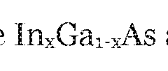 and GaAs formed on GaAs/Si base structure, formed on InP formed on GaAs/Si base and GeSiSn

on Si.
It will be appreciated that many modifications maybe made to the embodiments hereinbefore described.
A layer need not be homogeneous, that is, have a constant stoichiometry or
composition throughout the thickness of a layer. For example, a layer may have graded or changing compositions. The composition may vary continuously or in steps. Thus, for example, an alloy (which may be binary, tertiary or greater) may comprise a first components A and B in a ratio x and l-x and x may vary: x may vary monotonically in
the layer, for example, starting with a first value of x and ending with a second, different value of x, or vary non- monotonically.
Claims
1. A method of growing a heterostructure, the method comprising:
growing an epitaxial multilayer structure (106) on a base structure (102), the multilayer structure comprising:
a dislocation filter layer structure (107) comprising a stack of at least two dislocation filter layers (109, 110),
wherein the method comprises:
providing at least one layer (111) in the dislocation filter layer structure for inhibiting movement of threading dislocations, wherein the threading dislocation movement inhibiting layer is interposed between two dislocation filter layers;
relaxing each layer in the dislocation filter layer structure before growing a subsequent layer such that, for each layer in the dislocation filter layer structure:
misfit strain-thickness product εoh is equal to or greater than the equilibrium strain-thickness product εhc when the underlying layer is relaxed; and
strain-thickness product εh is equal to or less than the critical strain-thickness product (εh)* for dislocation multiplication during growth.
2. A method according to claim 1, wherein, the multilayer structure further comprises:
a device layer structure (108) disposed on the dislocation filter structure comprising at least one layer
wherein the method comprises:
relaxing each layer in the device layer structure before growing a subsequent layer such that, for each layer in the device layer structure:
misfit strain-thickness product εoh is equal to or greater than the equilibrium strain-thickness product εhc when the underlying layer is relaxed; and
strain-thickness product εh is equal to or less than the critical strain-thickness product (εh)* for dislocation multiplication during growth.
3. A method of growing a heterostructure, the method comprising:
growing a device layer structure (108) comprising at least one layer on a dislocation filter layer structure (107) comprising a stack of at least two dislocation filter layers (109, 110) and at least one layer (111) for inhibiting movement of threading dislocations, wherein the threading dislocation movement inhibiting layer is interposed between two dislocation filter layers;
wherein the method comprises:
relaxing each layer in the device layer structure before growing a subsequent layer such that, for each layer in the device layer structure:
misfit strain-thickness product εoh is equal to or greater than the equilibrium strain-thickness product εhc when the underlying layer is relaxed; and
strain-thickness product εh is equal to or less than the critical strain-thickness product (εh)* for dislocation multiplication during growth.
4. A method according to any preceding claim, wherein relaxing a layer comprises: growing a layer sufficiently slowly that relaxation takes place xnsitu.
5. A method according to any preceding claim, wherein relaxing a layer comprises: pausing growth of the layer, waiting for a given time and resuming growth of the layer.
6. A method according to any preceding claim, wherein relaxing a layer comprises: growing the layer, then waiting for a given time until the layer has relaxed.
7. A method according to claim 5 or 6, wherein the given time exceeds a threshold time which is dependent on dislocation velocity.
8. A method according to any preceding claim, wherein relaxing a layer comprises: annealing the layer.
9. A method according to any preceding claim, wherein providing the threading dislocation movement inhibiting layer comprises:
growing a layer of quantum dots.
10. A method according to any preceding claim, wherein providing the threading dislocation movement inhibiting layer comprises:
introducing dopants.
11. A method according to any preceding claim, wherein providing the threading dislocation movement inhibiting layer comprises:
implanting ions.
12. A method according to any preceding claim, wherein providing the threading dislocation movement inhibiting layer comprises:
depositing a non-continuous layer of material.
13. A method according to any preceding claim, wherein providing the threading dislocation movement inhibiting layer comprises:
forming the threading dislocation movement inhibiting layer after growing a dislocation filter layer and before growing a subsequent dislocation filter layer.
14. A method according to claim 13, wherein providing the threading dislocation movement inhibiting layer comprises:
forming the threading dislocation movement inhibiting layer after annealing the dislocation filter layer.
15. A method according to any preceding claim, wherein the base structure comprises a heterostructure comprising a substrate (103) and an uppermost layer (104).
16. A method according to claim 15, wherein the uppermost layer (104) has a threading dislocation density pro at least 108 cm-2 and the device layer structure (108) has a threading dislocation density pro no more than ios cm-2.
17. A heterostructure (101) comprising:
a base structure (102); and
an epitaxial multilayer structure (106) disposed directly on base structure, the multilayer structure comprising:
a dislocation filter layer structure (107) comprising a stack of at least two layers (109, 110) comprising first and second different materials respectively, wherein:
misfit strain-thickness product εoh for each layer in the epitaxial multilayer structure is equal to or exceeds the equilibrium strain-thickness product εh for the respective layer when the underlying layer is relaxed; and
strain-thickness product εh for each layer in the epitaxial multilayer structure does not exceed the critical strain-thickness product (εh)* for dislocation
multiplication.
18. A heterostructure according to claim 17, wherein the multilayer structure further comprises:
a device layer structure (108) disposed on the dislocation filter structure comprising at least one layer.
19. A heterostructure (101) comprising:
a base structure (102);
an epitaxial multilayer structure (106) disposed on a base structure (102), the multilayer structure comprising:
a dislocation filter layer structure (107) comprising a stack of at least two dislocation filter layers (109, 110); and
a device layer structure (108) disposed on the dislocation filter structure comprising at least one layer,
the heterostructure further comprising:
at least one layer in the dislocation filter layer structure for inhibiting movement of threading dislocations, wherein the threading dislocation movement inhibiting layer is interposed between two dislocation filter layers;
wherein for each layer in the epitaxial multilayer structure:
misfit strain-thickness product εoh is equal to or greater than the equilibrium strain-thickness product εhc when the underlying layer is relaxed; and
strain-thickness product εh is equal to or less than the critical strain-thickness product (εh)* for dislocation multiplication.
20. A heterostructure according to claim 19, wherein the base structure (102) is a heterostructure comprising:
a substrate (103); and
an uppermost layer (104) disposed on the substrate (103).
21. A heterostructure according to claim 20, wherein the uppermost layer (104) has a threading dislocation density pro at least 108 cm-2 and the device layer structure (108) has a threading dislocation density pro no more than 105 cm-2
Applications Claiming Priority (2)
| Application Number | Priority Date | Filing Date | Title |
|---|---|---|---|
| GB1604689.8 | 2016-03-21 | ||
| GB1604689.8A GB2552444A (en) | 2016-03-21 | 2016-03-21 | Heterostructure |
Publications (1)
| Publication Number | Publication Date |
|---|---|
| WO2017163034A1 true WO2017163034A1 (en) | 2017-09-28 |
Family
ID=55968586
Family Applications (1)
| Application Number | Title | Priority Date | Filing Date |
|---|---|---|---|
| PCT/GB2017/050769 Ceased WO2017163034A1 (en) | 2016-03-21 | 2017-03-20 | Heterostructure |
Country Status (2)
| Country | Link |
|---|---|
| GB (1) | GB2552444A (en) |
| WO (1) | WO2017163034A1 (en) |
Cited By (1)
| Publication number | Priority date | Publication date | Assignee | Title |
|---|---|---|---|---|
| CN112885921A (en) * | 2021-01-14 | 2021-06-01 | 常州信息职业技术学院 | GaInP/GaAs/AlGaSb triple-junction cascade solar cell and preparation method thereof |
Citations (3)
| Publication number | Priority date | Publication date | Assignee | Title |
|---|---|---|---|---|
| US338589A (en) | 1886-03-23 | Peters | ||
| EP1014431A2 (en) * | 1998-12-22 | 2000-06-28 | DaimlerChrysler AG | Method of fabricating epitaxial silicon-germanium layers |
| EP2897157A1 (en) * | 2014-01-15 | 2015-07-22 | Kabushiki Kaisha Toshiba | Nitride semiconductor element and nitride semiconductor wafer |
Family Cites Families (6)
| Publication number | Priority date | Publication date | Assignee | Title |
|---|---|---|---|---|
| FR2650704B1 (en) * | 1989-08-01 | 1994-05-06 | Thomson Csf | PROCESS FOR THE MANUFACTURE BY EPITAXY OF MONOCRYSTALLINE LAYERS OF MATERIALS WITH DIFFERENT MESH PARAMETERS |
| US5183778A (en) * | 1989-11-20 | 1993-02-02 | Fujitsu Limited | Method of producing a semiconductor device |
| US5208182A (en) * | 1991-11-12 | 1993-05-04 | Kopin Corporation | Dislocation density reduction in gallium arsenide on silicon heterostructures |
| US20010042503A1 (en) * | 1999-02-10 | 2001-11-22 | Lo Yu-Hwa | Method for design of epitaxial layer and substrate structures for high-quality epitaxial growth on lattice-mismatched substrates |
| JP2007534146A (en) * | 2003-09-05 | 2007-11-22 | ザ・ユニバーシティ・オブ・ノース・カロライナ・アット・シャーロット | Quantum dot optoelectronic device epitaxially grown in nanoscale and method for manufacturing the same |
| US20150236179A1 (en) * | 2014-02-19 | 2015-08-20 | Jun Yang | Filtering defects with strain-compensated multi-layer quantum dots |
-
2016
- 2016-03-21 GB GB1604689.8A patent/GB2552444A/en not_active Withdrawn
-
2017
- 2017-03-20 WO PCT/GB2017/050769 patent/WO2017163034A1/en not_active Ceased
Patent Citations (3)
| Publication number | Priority date | Publication date | Assignee | Title |
|---|---|---|---|---|
| US338589A (en) | 1886-03-23 | Peters | ||
| EP1014431A2 (en) * | 1998-12-22 | 2000-06-28 | DaimlerChrysler AG | Method of fabricating epitaxial silicon-germanium layers |
| EP2897157A1 (en) * | 2014-01-15 | 2015-07-22 | Kabushiki Kaisha Toshiba | Nitride semiconductor element and nitride semiconductor wafer |
Non-Patent Citations (4)
| Title |
|---|
| D. J. DUNSTAN: "Strain and strain relaxation in semiconductors", JOURNAL OF MATERIALS SCIENCE: MATERIALS IN ELECTRONICS, vol. 8, 1997, pages 337 - 375, XP055374693, DOI: doi:10.1023/A:1018547625106 |
| RICHARD BEANLAND: "Multiplication of misfit dislocations in epitaxial layers", JOURNAL OF APPLIED PHYSICS, vol. 72, 1992, pages 4031 |
| WARD T ET AL: "Design rules for dislocation filters", JOURNAL OF APPLIED PHYSICS, AMERICAN INSTITUTE OF PHYSICS, US, vol. 116, no. 6, 14 August 2014 (2014-08-14), XP012188636, ISSN: 0021-8979, [retrieved on 19010101], DOI: 10.1063/1.4892162 * |
| ZETIAN MI ET AL: "High-Performance Quantum Dot Lasers and Integrated Optoelectronics on Si", PROCEEDINGS OF THE IEEE, IEEE. NEW YORK, US, vol. 97, no. 7, July 2009 (2009-07-01), pages 1239 - 1249, XP011262464, ISSN: 0018-9219 * |
Cited By (1)
| Publication number | Priority date | Publication date | Assignee | Title |
|---|---|---|---|---|
| CN112885921A (en) * | 2021-01-14 | 2021-06-01 | 常州信息职业技术学院 | GaInP/GaAs/AlGaSb triple-junction cascade solar cell and preparation method thereof |
Also Published As
| Publication number | Publication date |
|---|---|
| GB201604689D0 (en) | 2016-05-04 |
| GB2552444A (en) | 2018-01-31 |
Similar Documents
| Publication | Publication Date | Title |
|---|---|---|
| TWI222106B (en) | Semiconductor substrate, field-effect transistor, and their production methods | |
| US9773906B2 (en) | Relaxed semiconductor layers with reduced defects and methods of forming the same | |
| US5221367A (en) | Strained defect-free epitaxial mismatched heterostructures and method of fabrication | |
| Imura et al. | High-temperature metal-organic vapor phase epitaxial growth of AlN on sapphire by multi transition growth mode method varying V/III ratio | |
| KR101899742B1 (en) | Semiconductor structure comprising an active semiconductor layer of the iii-v type on a buffer layer stack and method for producing semiconductor structure | |
| KR102313428B1 (en) | Method for separating the semiconductor substrate body and the functional layer thereon | |
| EP2553716B1 (en) | Iii-v semiconductor structures and methods for forming the same | |
| KR101186032B1 (en) | Method for manufacturing a layer of gallium nitride or gallium and aluminum nitride | |
| TWI521733B (en) | Method for producing a gallium-containing group III nitride semiconductor | |
| CN107810544A (en) | Stress Control in Heteroepitaxial | |
| KR100671279B1 (en) | Deformed Silicon Wafer and Manufacturing Method Thereof | |
| JP6812333B2 (en) | Compound semiconductor substrate | |
| KR101226073B1 (en) | Strain engineered composite semiconductor substrates and methods of forming same | |
| US10121656B2 (en) | Buffer layers having composite structures | |
| US10236338B2 (en) | SiC single crystal seed, SiC ingot, SiC single crystal seed production method, and SiC single crystal ingot production method | |
| WO2017163034A1 (en) | Heterostructure | |
| JP2008523635A (en) | Semiconductor substrate, semiconductor device, and semiconductor substrate manufacturing method | |
| KR20190122816A (en) | Group III-nitride structures with successively reduced crystallographic dislocation density regions | |
| Ting et al. | Range of Defect Morphologies on GaAs grown on offcut (001) Ge substrates | |
| TW201836021A (en) | Heterostructure | |
| Simpson et al. | On the use of low energy misfit dislocation structures to filter threading dislocations in epitaxial heterostructures | |
| Tikhonov et al. | TEM study of defects in AlxGa1− xN layers with different polarity | |
| CN205406555U (en) | Nitride buffer layer with composite construction | |
| KR20140055337A (en) | Epitaxial wafer and method for fabricating the same | |
| JP4208237B2 (en) | Manufacturing method of semiconductor substrate |
Legal Events
| Date | Code | Title | Description |
|---|---|---|---|
| NENP | Non-entry into the national phase |
Ref country code: DE |
|
| 121 | Ep: the epo has been informed by wipo that ep was designated in this application |
Ref document number: 17713763 Country of ref document: EP Kind code of ref document: A1 |
|
| 122 | Ep: pct application non-entry in european phase |
Ref document number: 17713763 Country of ref document: EP Kind code of ref document: A1 |