WO2017150491A1 - Ad変換結果読出回路 - Google Patents
Ad変換結果読出回路 Download PDFInfo
- Publication number
- WO2017150491A1 WO2017150491A1 PCT/JP2017/007642 JP2017007642W WO2017150491A1 WO 2017150491 A1 WO2017150491 A1 WO 2017150491A1 JP 2017007642 W JP2017007642 W JP 2017007642W WO 2017150491 A1 WO2017150491 A1 WO 2017150491A1
- Authority
- WO
- WIPO (PCT)
- Prior art keywords
- conversion result
- read
- register
- conversion
- identification data
- Prior art date
- Legal status (The legal status is an assumption and is not a legal conclusion. Google has not performed a legal analysis and makes no representation as to the accuracy of the status listed.)
- Ceased
Links
Images




Classifications
-
- G—PHYSICS
- G06—COMPUTING OR CALCULATING; COUNTING
- G06F—ELECTRIC DIGITAL DATA PROCESSING
- G06F3/00—Input arrangements for transferring data to be processed into a form capable of being handled by the computer; Output arrangements for transferring data from processing unit to output unit, e.g. interface arrangements
- G06F3/05—Digital input using the sampling of an analogue quantity at regular intervals of time, input from a/d converter or output to d/a converter
-
- G—PHYSICS
- G06—COMPUTING OR CALCULATING; COUNTING
- G06F—ELECTRIC DIGITAL DATA PROCESSING
- G06F15/00—Digital computers in general; Data processing equipment in general
- G06F15/76—Architectures of general purpose stored program computers
- G06F15/78—Architectures of general purpose stored program computers comprising a single central processing unit
Definitions
- the present invention relates to an AD conversion result reading circuit for reading an AD conversion result from an AD converter.
- Non-Patent Document 1 and Non-Patent Document 2 In a conventional general ⁇ type AD converter, when reading the AD conversion result from the CPU (Central Processing Unit) by SPI (Serial Peripheral Interface), the DRDY signal indicating the conversion state is monitored, and the falling edge of the DRDY signal is monitored.
- the SPI master must be designed so that the AD conversion result is read during the period from the detection of the detection to the completion of the next conversion (see Non-Patent Document 2).
- This restriction is provided if the timing of reading the conversion result of the SPI master is delayed due to other processing after detecting the falling edge of the DRDY signal, the next AD conversion result is updated. This is because reading from the SPI master collides, and the read AD conversion result becomes an indefinite value. Furthermore, there is no method for determining / confirming that the AD conversion result has become an indefinite value in the AD converter. Therefore, when reading the AD conversion result, a delay in timing is absolutely not allowed, and the designer of the CPU constituting the SPI master as an external device has to perform extremely strict time management.
- the present invention has been made to solve the above-described problems, and has an object to reduce the burden of timing design on the designer. It is another object of the present invention to provide an AD conversion result reading circuit that can alleviate performance required for a CPU constituting an external device.
- the AD conversion result reading circuit of the present invention makes the detection signal valid when it receives a high-order bit of a command from an external device that is a transmission destination of the AD conversion result of the AD converter and determines that it is a read command.
- a detection circuit that validates the transmission permission signal when all the commands are received and confirmed as a read command, and an internal register synchronized with the clock of the AD converter in accordance with the detection signal synchronized with the clock of the external device AD conversion of the AD converter when the clock change circuit for outputting the value change prohibition signal and the data preparation completion signal from the AD converter are valid and the internal register value change prohibition signal is invalid
- the AD conversion result can be sent to the external device without giving any special restriction to the external device.
- the AD conversion result can be sent to the external device without giving any special restriction to the external device.
- it is possible to reduce the burden of timing design on the designer.
- the performance required for the CPU constituting the external device can be relaxed.
- FIG. 1 is a block diagram showing a configuration of an AD conversion result reading circuit according to the first embodiment of the present invention.
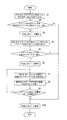
- FIG. 2 is a flowchart for explaining the operation of the READ detection circuit of the AD conversion result reading circuit according to the first embodiment of the present invention.
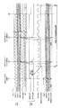
- FIG. 3 is a timing chart for explaining the operation of each part of the AD conversion result read circuit according to the first embodiment of the present invention.
- FIG. 4 is a block diagram showing a configuration example of the clock transposing circuit of the AD conversion result reading circuit according to the first embodiment of the present invention.
- FIG. 5 is a timing chart for explaining a timing relationship for preventing the metastable state.
- FIG. 6 is a timing chart for explaining a timing relationship for preventing the metastable state.
- FIG. 5 is a timing chart for explaining a timing relationship for preventing the metastable state.
- FIG. 7 is a timing chart showing the operation when the clock frequency on the AD converter side is increased in the conventional AD conversion result reading circuit.
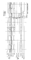
- FIG. 8 is a timing chart for explaining the operation of each part of the AD conversion result read circuit according to the second embodiment of the present invention.
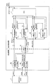
- FIG. 9 is a block diagram showing a configuration of an AD conversion result reading circuit according to the third embodiment of the present invention.
- FIG. 1 is a block diagram showing a configuration of an AD conversion result reading circuit according to the first embodiment of the present invention.
- the AD conversion result reading circuit according to the present embodiment includes AD conversion result registers 2 and 3 for temporarily storing the AD conversion result of the AD converter (hereinafter referred to as ADC) 1 and an SPI master 7 which is an external device.
- ADC AD conversion result registers 2 and 3 for temporarily storing the AD conversion result of the AD converter (hereinafter referred to as ADC) 1 and an SPI master 7 which is an external device.
- READ detection that makes the detection signal valid when the upper bit of the command is received and is determined to be a read command, and enables the transmission permission signal when all commands from the SPI master 7 are received and confirmed as a read command
- the SPI master 7 the clock transfer circuit 5 that outputs the internal register value change prohibition signal synchronized with the clock of the ADC 1, and when the transmission permission signal is valid, From the data transmission circuit 6 that reads the AD conversion result from the AD conversion result register 2 and transmits it to the SPI master 7 It is made.
- FIG. 2 is a flowchart for explaining the operation of the READ detection circuit 4.
- FIG. 3 is a timing chart for explaining the operation of each part of the AD conversion result reading circuit.
- the clock of the ADC 1 is CLK_REG
- the clock of the SPI master 7 composed of the CPU is SCLK.
- the AD conversion result registers 2 and 3 and the clock transfer circuit 5 operate in synchronization with CLK_REG
- the READ detection circuit 4 and the clock transfer circuit 5 The data transmission circuit 6 operates in synchronization with SCLK.
- CS is a chip select signal
- MOSI Master (Out Slave In) and MISO (Master In Slave Out) are signal lines of the SPI master 7
- SCLK_INV is an inverted signal of the clock SCLK
- READ_ACT is a detection signal of a read command
- RDATA_EN Is an AD conversion result transmission enable signal
- READ_ACT_SYNC is an internal register value change prohibition signal
- DRDY is a data preparation completion signal for ADC1
- RESULT is an AD conversion result output from ADC1
- RESULT_BUF is stored in AD conversion result register 3
- the AD conversion result, RESULT_LATCH represents the AD conversion result stored in the AD conversion result register 2.
- the READ detection circuit 4 receives the upper 3 bits of the command (step S1 in FIG. 2), and the upper order of this command. It is determined whether the 3 bits match the upper 3 bits of the RDATA * command, that is, the upper 3 bits of the AD conversion result read command (step S2 in FIG. 2).
- C7 to C5 are the upper 3 bits of the command, and determination is performed at time t1. The reason for performing the determination with the upper 3 bits will be described later.
- the READ detection circuit 4 sets the detection signal READ_ACT to “1” (valid) ( Step S3 in FIG.
- the READ detection circuit 4 receives the lower 5 bits of the command from the SPI master 7 and receives all the 8-bit commands (step S4 in FIG. 2)
- the 8-bit command is the RDATA * command, that is, the AD conversion result. It is determined whether or not the read command matches (step S5 in FIG. 2). In the example of FIG. 3, C4 to C0 are the lower 5 bits of the command.
- the READ detection circuit 4 keeps the detection signal READ_ACT to “1” (step S6 in FIG. 2), and transmits a transmission permission signal. Issue one pulse of RDATA_EN.
- the data transmission circuit 6 When one pulse of the transmission enable signal RDATA_EN is issued, the data transmission circuit 6 reads the AD conversion result for 8 bits from the AD conversion result register 2 (step S7 in FIG. 2), and performs AD conversion for this 8 bits. The result is serially transmitted as transmission data to the SPI master 7 via the signal line MISO (step S8 in FIG. 2). In the example of FIG. 3, the AD conversion result for 8 bits D0 to D7 is transmitted to the SPI master 7 as transmission data in response to the transmission permission signal RDATA_EN at time t3.
- the READ detection circuit 4 determines whether or not the transmission of the number of data corresponding to the command, for example, the transmission of the AD conversion result has been completed (step S9 in FIG. 2). When the determination result in step S9 is “N”), the process returns to step S7 to issue one pulse of the transmission permission signal RDATA_EN again.
- the data transmission circuit 6 reads the AD conversion result for another 8 bits from the AD conversion result register 2 and serially transmits it to the SPI master 7 (step of FIG. 2). S8).
- the AD conversion result for 8 bits D8 to D15 is transmitted to the SPI master 7 as transmission data in response to the transmission permission signal RDATA_EN at time t4.
- steps S7 and S8 are repeatedly executed until the transmission of the number of data corresponding to the command, that is, the transmission of the AD conversion result is completed.
- the AD conversion result sent in response to the read command from the SPI master 7 is 24 bits. Therefore, when the transmission permission signal RDATA_EN is issued three times and the transmission of 24-bit data D0 to D23 is completed, the determination result in step S9 becomes “Y” (time t5).
- the READ detection circuit 4 sets the detection signal READ_ACT to “0” (invalid) (step S10 in FIG. 2).
- the READ detection circuit 4 sets the detection signal READ_ACT to “0” (invalid) when it receives all the commands from the external device and determines that it is not a read command after setting the detection signal READ_ACT to “1” (valid). Also good. This is because even if the upper 3 bits of the command from the SPI master 7 coincide with the upper 3 bits of the read command in the determination in step S2, the determination may be wrong.
- step S3 in FIG. 2 8 bits in step S5
- the detection signal READ_ACT is set to “0”. The determination result made in steps S2 and S3 is canceled.
- the AD conversion result register 2 Since the internal register value change prohibition signal READ_ACT_SYNC at this time is “0” (invalid), indicating that a read command has not been detected, the AD conversion result RESULT from the ADC 1 is fetched. As described above, the AD conversion result RESULT is 24 bits.
- the fetched AD conversion result RESULT is stored in the AD conversion result register 2, and the output RESULT_LATCH of the AD conversion result register 2 is updated.
- RESULT_LATCH is updated from “OLD” indicating the old conversion result to “NEW” indicating the newly acquired conversion result.
- FIG. 4 is a block diagram showing a configuration example of the clock transfer circuit 5.
- the clock transfer circuit 5 includes two flip-flops 50 and 51. As shown in FIG. 4, the flip-flop 51 is connected in cascade with the flip-flop 50, and these two flip-flops 50 and 51 are driven by the clock CLK_REG of the ADC1.
- the internal register value change prohibition signal READ_ACT_SYNC is delayed by a maximum of twice the period of CLK_REG with respect to the detection signal READ_ACT.
- the internal register value change prohibition signal READ_ACT_SYNC becomes “1” (valid) at time t2.
- the internal register value change prohibition signal READ_ACT_SYNC becomes “0” (invalid) at time t6.
- the time difference between times t1 and t2 and the time difference between times t5 and t6 are delays caused by the clock transfer circuit 5 shown in FIG.
- the SPI master 7 reads the conversion result without considering the conversion cycle of the ADC 1, the data may be destroyed and correct data may not be read.
- the reason why the data is destroyed is that the relationship between the clock SCLK of the SPI master 7 and the clock CLK_REG of the ADC 1 is asynchronous. Therefore, when data is transferred based on different clocks, the rising edges of these two clocks happen to occur. This is because the setup / hold timing of the flip-flop cannot be satisfied when approaching. This phenomenon is called “metastable”. For the metastable, see, for example, “Column: Asynchronous Clock and Verification Method-2”, Altima Co., Ltd. ⁇ http://www.altima.jp/products/software/mentor/fv/column/cdc-2.html > ”.
- FIG. 5 and FIG. 6 are timing charts for explaining the timing of replacing the clock while preventing this metastable.
- FIG. 5 shows a case where the clock transfer time becomes short (when the clock CLK_REG rises immediately after the rise of the detection signal READ_ACT), and
- FIG. 6 shows a case where the clock transfer time becomes long (just after the rise of the clock CLK_REG) When standing up).
- the internal register value change prohibition signal READ_ACT_SYNC is set to “1” (valid) before the transmission timing of the AD conversion result to the SPI master 7, and the register value does not change during transmission of the AD conversion result. Need to be controlled. That is, T1> T2 must be satisfied in FIGS.
- T1 is a time from when the detection signal READ_ACT becomes “1” until the transmission permission signal RDATA_EN becomes “1” (valid), and T2 is a time required for clock replacement.
- FIG. 7 shows an operation when the frequency of the clock CLK_REG is sufficiently increased in the conventional AD conversion result reading circuit.
- the detection signal READ_ACT is set to “1” after all the 8-bit commands C7 to C0 are read. In this way, if the clock CLK_REG is made sufficiently fast, the detection signal READ_ACT need not be set to “1” by prefetching. However, since the clock CLK_REG becomes high speed, there is a problem that power consumption increases.
- the internal register value change prohibition signal READ_ACT_SYNC is always “1” when the transmission permission signal RDATA_EN becomes “1” (valid). Therefore, the output RESULT_LATCH of the AD conversion result register 2 does not change at the AD conversion result transmission timing (t3 and t4 in the example of FIG. 3). That is, no metastable occurs.
- the AD conversion result can be transmitted to the SPI master 7 without giving any special restriction to the SPI master 7, so that the timing design burden of the designer is reduced.
- the performance required for the SPI master 7 (CPU) can be reduced.
- the AD conversion result becomes an indefinite value by preventing the output RESULT_LATCH of the AD conversion result register 2 from being changed at the timing when the transmission permission signal RDATA_EN becomes “1”. Therefore, it is possible to protect the AD conversion result without increasing the frequency of the clock CLK_REG of the ADC 1.
- the determination in step S2 is performed with upper multiple bits, specifically, the upper 3 bits.
- the present invention is not limited to this, and the determination in step S2 may be performed with only the most significant bit. It is possible.
- the AD conversion result reading circuit uses an AD conversion result register 3 in addition to the AD conversion result register 2 used in the first embodiment. More specifically, in addition to the first AD conversion result register 2, when the data preparation completion signal from the ADC 1 is valid and the internal register value change prohibition signal READ_ACT_SYNC is valid, the ADC 1 A second AD conversion result register 3 for fetching the AD conversion result is provided. The first AD conversion result register 2 is used for the second AD conversion result when the internal register value change prohibition signal READ_ACT_SYNC is invalidated. The output of the register 3 is fetched.
- FIG. 8 is a timing chart for explaining the operation of each part of the AD conversion result readout circuit of this embodiment.
- the AD conversion result register 2 has an internal register in which the data preparation completion signal DRDY output from the ADC 1 falls from “1” (invalid) to “0” (valid). If the value change prohibition signal READ_ACT_SYNC is “0” (invalid), the AD conversion result RESULT of the ADC 1 is fetched. As a result, the output RESULT_LATCH of the AD conversion result register 2 is updated.
- the internal register value change prohibition signal READ_ACT_SYNC is already “1” (valid).
- the first AD conversion result register 2 cannot capture the AD conversion result RESULT of the ADC 1. Accordingly, the output RESULT_LATCH of the first AD conversion result register 2 cannot be updated. That is, in the first and second embodiments, the interval in which the internal register value change prohibition signal READ_ACT_SYNC is “1” (valid) is the internal register value change prohibition interval.
- the second AD conversion result register 3 is used. That is, in the second AD conversion result register 3, the data preparation completion signal DRDY output from the ADC 1 falls from “1” (invalid) to “0” (valid), and the internal register value change prohibition signal READ_ACT_SYNC is If “1” (valid), the AD conversion result RESULT of ADC 1 is fetched. As a result, the output RESULT_BUF of the second AD conversion result register 3 is updated. According to the example of FIG. 8, it is understood that RESULT_BUF is updated to “NEW” indicating the newly acquired conversion result.
- the first AD conversion result register 2 takes in the output RESULT_BUF of the second AD conversion result register 3 ( Time t7).
- the output RESULT_LATCH of the first AD conversion result register 2 is updated.
- RESULT_LATCH is updated from “OLD” indicating the old conversion result to “NEW” indicating the newly acquired conversion result.
- Other configurations are the same as those described in the first embodiment.
- the internal register value change prohibition signal READ_ACT_SYNC is already “1”. Then, since the first AD conversion result register 2 cannot capture the AD conversion result of the ADC 1, there is a possibility that the AD conversion result may be missed.
- the second AD conversion result register 3 by providing the second AD conversion result register 3, the second AD conversion result register 2 cannot receive the AD conversion result in the second AD conversion result register 2. Since the AD conversion result register 3 takes in the AD conversion result, it is possible to avoid the occurrence of missing of the AD conversion result.
- FIG. 9 is a block diagram showing a configuration of an AD conversion result read circuit according to the third embodiment.
- the AD conversion result reading circuit according to the third embodiment includes AD conversion result registers 2 and 3, a READ detection circuit 4a, a clock transfer circuit 5, a data transmission circuit 6a, an identification data register 8, 9. More specifically, in the AD conversion result reading circuit according to the third embodiment, in addition to the configuration of the AD conversion result reading circuit according to the first or second embodiment, data preparation from the ADC 1 is completed.
- the first identification data register 8 that takes in the identification data associated with the AD conversion result from the ADC 1
- the data transmission circuit 6a reads the AD conversion result from the first AD conversion result register 2 and transmits it to the external device when the transmission permission signal RDATA_EN is “1” (valid).
- the identification data is read from one identification data register 8 and transmitted to the external device.
- the AD conversion result reading circuit when the data preparation completion signal DRDY from the ADC 1 is valid and the internal register value change prohibition signal READ_ACT_SYNC is “1” (valid).
- the first identification data register 8 has a second register when the internal register value change inhibition signal READ_ACT_SYNC becomes “0” (invalid). The output of the identification data register 9 may be captured.
- the ADC 1 outputs identification data DID associated with the AD conversion result RESULT in addition to the AD conversion result RESULT. Further, after completing the transmission of the AD conversion result for 24 bits, the READ detection circuit 4a issues one pulse of the transmission permission signal RDATA_EN for transmitting, for example, 8-bit identification data DID (step S7 in FIG. 2). In response to the transmission permission signal RDATA_EN, the data transmission circuit 6a reads the identification data DID from the identification data register 8 and serially transmits it to the SPI master 7 (step S8 in FIG. 2).
- the processing of steps S7 and S8 in FIG. 2 is repeated until transmission of 8-bit identification data DID, that is, 32-bit data in total, in addition to the 24-bit AD conversion result is completed. Will be executed.
- 8-bit identification data DID is transmitted.
- Other operations of the READ detection circuit 4a are the same as those of the READ detection circuit 4 in the first and second embodiments.
- the identification data register 8 the data preparation completion signal DRDY output from the ADC 1 falls from “1” (invalid) to “0” (valid), and the internal register value change prohibition signal READ_ACT_SYNC is “0” (invalid). If so, the identification data DID output from the ADC 1 is captured. Thus, the output DID_LATCH of the identification data register 8 is updated.
- the identification data register 8 is already prohibited from changing the internal register value when the data preparation completion signal DRDY output from the ADC 1 falls from “1" to "0".
- the signal READ_ACT_SYNC is “1” (valid)
- the identification data DID cannot be captured.
- the identification data register 9 outputs from the ADC 1
- the identification data DID is captured.
- the output DID_BUF of the identification data register 9 is updated.
- the identification data register 8 takes in the output DID_BUF of the identification data register 9 when the internal register value change prohibition signal READ_ACT_SYNC changes from “1” to “0”.
- the identification data register 8 performs the same operation as the AD conversion result register 2 for the identification data DID
- the identification data register 9 performs the same operation as the second AD conversion result register 3.
- identification data DID will be described in detail. Examples of the method for generating the identification data DID include the following four methods.
- the first example is a technique in which data based on the number of executions of AD conversion processing is used as identification data DID.
- the identification data is data indicating the number of executions of AD conversion processing by the ADC 1.
- the number of executions of the AD conversion process may be counted in the ADC 1 and the count value may be used as the identification data DID.
- the AD conversion result by the AD conversion process executed at a certain timing and the AD conversion result by the AD conversion process executed at the timing before and after the AD conversion process are obtained. Can be identified.
- the second example is a method in which data based on the execution time of the AD conversion process, for example, data indicating the time when the AD conversion process is executed by the ADC 1 is used as the identification data DID.
- the ADC 1 may set the execution time (time stamp) of the AD conversion process as the identification data DID.
- One is a method of providing a real-time clock inside or outside the ADC 1.
- the other is a method of providing a counter that is incremented at regular intervals, for example, at time 0 when the power is turned on, inside or outside the ADC 1 instead of the real-time clock.
- Either of the two methods described above makes it possible to distinguish between an AD conversion result by an AD conversion process executed at a certain timing and an AD conversion result by an AD conversion process executed at a timing before and after that. Furthermore, according to the above-described method using the real-time clock, it is possible to record the accurate time when the AD conversion process is executed. On the other hand, according to the technique that does not use the real-time clock described above, an increase in circuit scale can be suppressed.
- a third example is a technique in which 1-bit data whose logic level is inverted every time AD conversion processing is executed is used as identification data DID. That is, the identification data DID is 1-bit data whose logic level is inverted every time AD conversion processing is executed by the ADC 1. According to this method, it is possible to identify an AD conversion result by an AD conversion process executed at a certain timing and an AD conversion result by an AD conversion process executed at a timing before and after the AD conversion process. Further, since the identification data DID is 1 bit, the necessary hardware resources can be reduced, and an increase in circuit scale can be suppressed.
- the fourth example is a technique in which data based on the count value of the free-run counter is used as identification data DID.
- an 8-bit free-run counter may count pulses input continuously regardless of the execution process of the AD conversion process, and the count value may be used as the identification data DID. According to this, since a counter having a large bit width is not required, an increase in circuit scale can be suppressed.
- the data stored as the identification data DID does not have to be the count value (numerical value) of the free-run counter itself, but may be an alphabet (character code) whose order is known, such as AZ.
- identification data is assigned to each AD conversion result, and the AD conversion result and the identification data are output as a set. It is possible to determine whether the continuity of the AD conversion result is maintained.
- the first identification data register 8 is provided, and when the data transmission circuit 6a has the transmission permission signal RDATA_EN from the READ detection circuit 4a valid, the first identification data By reading the identification data from the register 8 and transmitting it to the external device, it is possible for the external device side to determine whether the AD conversion result has been duplicated or whether the AD conversion result has been missed. Furthermore, by providing the second identification data register 9, it is possible to avoid the occurrence of missing identification data.
- the SPI master 7 side determines whether or not there is, that is, whether or not the continuity of the acquired AD conversion results is maintained.
- the present invention can be applied to a technique for reading an AD conversion result without considering the conversion cycle of the AD converter.
Landscapes
- Engineering & Computer Science (AREA)
- Theoretical Computer Science (AREA)
- Computer Hardware Design (AREA)
- Physics & Mathematics (AREA)
- General Engineering & Computer Science (AREA)
- General Physics & Mathematics (AREA)
- Human Computer Interaction (AREA)
- Information Transfer Systems (AREA)
- Microcomputers (AREA)
- Analogue/Digital Conversion (AREA)
Abstract
AD変換結果読出回路は、SPIマスター(7)からのコマンドの上位ビットを受け取って読み出しコマンドと判定したときに検出信号READ_ACTを有効とし、コマンドを全て受け取って読み出しコマンドと確定したときに送信許可信号RDATA_ENを有効とするREAD検出回路(4)と、信号READ_ACTに応じて内部レジスタ値変更禁止信号READ_ACT_SYNCを出力するクロック載せ換え回路(5)と、AD変換器(1)からのデータ準備完了信号DRDYが有効であり、信号READ_ACT_SYNCが無効であるときに、AD変換結果を取り込むAD変換結果用レジスタ(2)と、信号RDATA_ENが有効であるときにAD変換結果をSPIマスター(7)へ送信するデータ送信回路(6)を備える。本発明によれば、設計者のタイミング設計の負担を軽減することができる。また、SPIマスター(7)に要求される性能を緩和することができる。
Description
本発明は、AD変換器からAD変換結果を読み出すAD変換結果読出回路に関する。
従来の一般的なΔΣ型AD変換器において、CPU(Central Processing Unit)などからSPI(Serial Peripheral Interface)によってAD変換結果を読み出す時には、変換状態を示すDRDY信号を監視して、DRDY信号の立ち下がりを検出してから次の変換完了までの期間にAD変換結果を読み出すように、SPIマスターを設計しなければならない(非特許文献1、非特許文献2参照)。
このような制約が設けられているのは、もしもDRDY信号の立ち下がりを検出してから他の処理が原因でSPIマスターの変換結果読み出しのタイミングが遅れてしまうと、次のAD変換結果の更新とSPIマスターからの読み出しがぶつかってしまい、読み出したAD変換結果が不定値になってしまうからである。さらに、AD変換結果が不定値となったことを判定・確認する方法がAD変換器に用意されていない。そのため、AD変換結果を読み出す際は絶対にタイミングの遅れが許されず、外部装置であるSPIマスターを構成するCPUの設計者は極めて厳密な時間管理を行わなければならなかった。
"温度センサ向け24ビット A/Dコンバータ ADS1248",日本テキサス・インスツルメンツ株式会社,2011年,<http://www.tij.co.jp/jp/lit/ds/symlink/ads1248.pdf>
"20μsセトリング、250kSPSの24ビットΣ-Δ ADC AD7176-2",アナログ・デバイセズ株式会社,2012年,<http://www.analog.com/media/jp/technical-documentation/data-sheets/AD7176-2_jp.pdf>
以上のように、従来は、AD変換結果を読み出すSPIマスターなどの外部装置を設計する設計者は、厳密な時間管理を行わなければならなかった。そのため、設計者にとっては、タイミング設計の負担が大きかった。また、外部装置には処理能力に余裕のあるCPUを選択せざるを得なかった。
本発明は、上記課題を解決するためになされたもので、設計者のタイミング設計の負担を軽減することを目的とする。また、外部装置を構成するCPUに要求される性能を緩和することができるAD変換結果読出回路を提供することを目的とする。
本発明のAD変換結果読出回路は、AD変換器のAD変換結果の送信先となる外部装置からのコマンドの上位ビットを受け取って読み出しコマンドと判定したときに検出信号を有効とし、前記外部装置からのコマンドを全て受け取って読み出しコマンドと確定したときに送信許可信号を有効とする検出回路と、前記外部装置のクロックと同期した前記検出信号に応じて、前記AD変換器のクロックと同期した内部レジスタ値変更禁止信号を出力するクロック載せ換え回路と、前記AD変換器からのデータ準備完了信号が有効であり、かつ前記内部レジスタ値変更禁止信号が無効であるときに、前記AD変換器のAD変換結果を取り込む第1のAD変換結果用レジスタと、前記送信許可信号が有効であるときに、前記第1のAD変換結果用レジスタからAD変換結果を読み出して前記外部装置へ送信するデータ送信回路とを備えることを特徴とする。
本発明によれば、検出回路とクロック載せ換え回路と第1のAD変換結果用レジスタとデータ送信回路とを設けることによって、外部装置に対して特別な制約を与えることなくAD変換結果を外部装置に送信することが可能となるので、設計者のタイミング設計の負担を軽減することができる。また、外部装置を構成するCPUに要求される性能を緩和することができる。
[第1の実施の形態]
以下、本発明の実施の形態について図面を参照して説明する。
図1は本発明の第1の実施の形態に係るAD変換結果読出回路の構成を示すブロック図である。本実施の形態のAD変換結果読出回路は、それぞれAD変換器(以下、ADC)1のAD変換結果を一時的に格納するAD変換結果用レジスタ2,3と、外部装置であるSPIマスター7からのコマンドの上位ビットを受け取って、これを読み出しコマンドと判定したときに検出信号を有効とし、SPIマスター7からのコマンドを全て受け取って読み出しコマンドと確定したときに送信許可信号を有効とするREAD検出回路4と、SPIマスター7のクロックと同期した検出信号に応じて、ADC1のクロックと同期した内部レジスタ値変更禁止信号を出力するクロック載せ換え回路5と、送信許可信号が有効であるときに、AD変換結果用レジスタ2からAD変換結果を読み出してSPIマスター7へ送信するデータ送信回路6とから構成される。
以下、本発明の実施の形態について図面を参照して説明する。
図1は本発明の第1の実施の形態に係るAD変換結果読出回路の構成を示すブロック図である。本実施の形態のAD変換結果読出回路は、それぞれAD変換器(以下、ADC)1のAD変換結果を一時的に格納するAD変換結果用レジスタ2,3と、外部装置であるSPIマスター7からのコマンドの上位ビットを受け取って、これを読み出しコマンドと判定したときに検出信号を有効とし、SPIマスター7からのコマンドを全て受け取って読み出しコマンドと確定したときに送信許可信号を有効とするREAD検出回路4と、SPIマスター7のクロックと同期した検出信号に応じて、ADC1のクロックと同期した内部レジスタ値変更禁止信号を出力するクロック載せ換え回路5と、送信許可信号が有効であるときに、AD変換結果用レジスタ2からAD変換結果を読み出してSPIマスター7へ送信するデータ送信回路6とから構成される。
なお、第1の実施の形態に係るAD変換結果読出回路は、二つのAD変換結果用レジスタ2,3を備えているが、本発明においては、いずれか1つを設ければよく、AD変換結果用レジスタを2つ設けることは必須の構成要件ではない。
次にAD変換結果読出回路の動作について、初めに1つのAD変換結果用レジスタ2のみを使った動作の例を図2、図3を用いて説明する。図2はREAD検出回路4の動作を説明するフローチャート、図3はAD変換結果読出回路の各部の動作を説明するタイミングチャートである。
本実施の形態では、ADC1のクロックをCLK_REG、CPUからなるSPIマスター7のクロックをSCLKとする。図1に示したAD変換結果読出回路の構成のうち、AD変換結果用レジスタ2,3とクロック載せ換え回路5とはCLK_REGに同期して動作し、READ検出回路4とクロック載せ換え回路5とデータ送信回路6とはSCLKに同期して動作する。
図3において、CSはチップセレクト信号、MOSI(Master Out Slave In)およびMISO(Master In Slave Out)はSPIマスター7の信号線、SCLK_INVはクロックSCLKの反転信号、READ_ACTは読み出しコマンドの検出信号、RDATA_ENはAD変換結果の送信許可信号、READ_ACT_SYNCは内部レジスタ値変更禁止信号、DRDYはADC1のデータ準備完了信号、RESULTはADC1から出力されるAD変換結果、RESULT_BUFはAD変換結果用レジスタ3に格納されたAD変換結果、RESULT_LATCHはAD変換結果用レジスタ2に格納されたAD変換結果をそれぞれ表す。
まず、CPUからなるSPIマスター7から信号線MOSIを介してコマンドが送出されると、READ検出回路4は、コマンドの上位3ビットを受け取った時点で(図2のステップS1)、このコマンドの上位3ビットがRDATA*コマンドの上位3ビット、すなわちAD変換結果の読み出しコマンドの上位3ビットと一致するかどうかを判定する(図2のステップS2)。図3の例では、C7~C5がコマンドの上位3ビットで、時刻t1の時点で判定を行っている。上位3ビットで判定を行う理由については後述する。
READ検出回路4は、SPIマスター7からのコマンドの上位3ビットが読み出しコマンドの上位3ビットと一致する場合(ステップS2においてY)には、検出信号READ_ACTを“1”(有効)に設定する(図2のステップS3)。
さらに、READ検出回路4は、SPIマスター7からコマンドの下位5ビットを受け取って8ビットのコマンドを全て受け取ると(図2のステップS4)、この8ビットのコマンドがRDATA*コマンド、すなわちAD変換結果の読み出しコマンドと一致するかどうかを判定する(図2のステップS5)。図3の例では、C4~C0がコマンドの下位5ビットである。
READ検出回路4は、SPIマスター7からの8ビットのコマンドが読み出しコマンドと一致する場合(ステップS5においてY)、検出信号READ_ACTを“1”のままとし(図2のステップS6)、送信許可信号RDATA_ENを1パルス発行する。
データ送信回路6は、送信許可信号RDATA_ENが1パルス発行されると、AD変換結果用レジスタ2から、AD変換結果を8ビット分読み出して(図2のステップS7)、この8ビット分のAD変換結果を送信データとして信号線MISOを介してSPIマスター7へシリアル送信する(図2のステップS8)。図3の例では、時刻t3の送信許可信号RDATA_ENに応じてD0~D7の8ビット分のAD変換結果が送信データとしてSPIマスター7へ送信される。
次に、READ検出回路4は、コマンドに対応した数のデータの送信、例えばAD変換結果の送信が完了したかどうかを判定し(図2のステップS9)、送信し終えていない場合には(ステップS9の判定結果が“N”)、ステップS7に戻って送信許可信号RDATA_ENを再び1パルス発行する。READ検出回路4が送信許可信号RDATA_ENを1パルス発行すると、データ送信回路6は、AD変換結果用レジスタ2からAD変換結果をさらに8ビット分読み出してSPIマスター7へシリアル送信する(図2のステップS8)。図3の例では、時刻t4の送信許可信号RDATA_ENに応じてD8~D15の8ビット分のAD変換結果が送信データとしてSPIマスター7へ送信される。
こうして、コマンドに対応した数のデータの送信、すなわちAD変換結果の送信が完了するまでステップS7,S8の処理が繰り返し実行される。本実施の形態では、SPIマスター7からの読み出しコマンドに応じて送るAD変換結果を24ビットとする。したがって、送信許可信号RDATA_ENが3回発行され、D0~D23の24ビットのデータを送信し終えた時点でステップS9の判定結果が“Y”となる(時刻t5)。
データの送信が完了してステップS9の判定結果が“Y”となると、READ検出回路4は、検出信号READ_ACTを“0”(無効)にする(図2のステップS10)。
なお、READ検出回路4は、検出信号READ_ACTを“1”(有効)とした後に、外部装置からのコマンドを全て受け取って読み出しコマンドでないと判定したときには、検出信号READ_ACTを“0”(無効)としてもよい。これは、ステップS2の判定においてSPIマスター7からのコマンドの上位3ビットが読み出しコマンドの上位3ビットと一致したとしても、判定を誤っている可能性があるからである。したがって、SPIマスター7からのコマンドの上位3ビットが読み出しコマンドの上位3ビットと一致して検出信号READ_ACTを“1”(有効)に設定した(図2のステップS3)後、ステップS5において8ビットのコマンドを全て解析した結果、SPIマスター7からの8ビットのコマンドが読み出しコマンドと一致しなかった場合には(図2のステップS5において“N”)、検出信号READ_ACTを“0”にして、ステップS2,S3で下した判定結果を取り消す。
なお、READ検出回路4は、検出信号READ_ACTを“1”(有効)とした後に、外部装置からのコマンドを全て受け取って読み出しコマンドでないと判定したときには、検出信号READ_ACTを“0”(無効)としてもよい。これは、ステップS2の判定においてSPIマスター7からのコマンドの上位3ビットが読み出しコマンドの上位3ビットと一致したとしても、判定を誤っている可能性があるからである。したがって、SPIマスター7からのコマンドの上位3ビットが読み出しコマンドの上位3ビットと一致して検出信号READ_ACTを“1”(有効)に設定した(図2のステップS3)後、ステップS5において8ビットのコマンドを全て解析した結果、SPIマスター7からの8ビットのコマンドが読み出しコマンドと一致しなかった場合には(図2のステップS5において“N”)、検出信号READ_ACTを“0”にして、ステップS2,S3で下した判定結果を取り消す。
次に、図3を参照して、ADC1のクロックCLK_REGに同期して動作する構成について説明する。
まず、ADC1から出力されるデータ準備完了信号DRDYが“1”(無効)から“0”(有効)に立ち下がり、ADC1のデータ準備が完了したことが通知されると、AD変換結果用レジスタ2は、このときの内部レジスタ値変更禁止信号READ_ACT_SYNCが“0”(無効)で、読み出しコマンドが検出されていないことを示しているため、ADC1からのAD変換結果RESULTを取り込む。上記のとおり、AD変換結果RESULTは24ビットである。取り込まれたAD変換結果RESULTは、AD変換結果用レジスタ2に記憶され、AD変換結果用レジスタ2の出力RESULT_LATCHが更新される。図3の例では、RESULT_LATCHが、古い変換結果を示す“OLD”から、新たに取り込んだ変換結果を示す“NEW”へと更新されることが示されている。
まず、ADC1から出力されるデータ準備完了信号DRDYが“1”(無効)から“0”(有効)に立ち下がり、ADC1のデータ準備が完了したことが通知されると、AD変換結果用レジスタ2は、このときの内部レジスタ値変更禁止信号READ_ACT_SYNCが“0”(無効)で、読み出しコマンドが検出されていないことを示しているため、ADC1からのAD変換結果RESULTを取り込む。上記のとおり、AD変換結果RESULTは24ビットである。取り込まれたAD変換結果RESULTは、AD変換結果用レジスタ2に記憶され、AD変換結果用レジスタ2の出力RESULT_LATCHが更新される。図3の例では、RESULT_LATCHが、古い変換結果を示す“OLD”から、新たに取り込んだ変換結果を示す“NEW”へと更新されることが示されている。
一方、クロック載せ換え回路5は、READ検出回路4から出力される検出信号READ_ACTに応じて、ADC1のクロックCLK_REGと同期した内部レジスタ値変更禁止信号READ_ACT_SYNCを生成する。
図4はクロック載せ換え回路5の構成例を示すブロック図である。クロック載せ換え回路5は、2つのフリップフロップ50,51によって構成される。図4に示すように、フリップフロップ51は、フリップフロップ50とカスケードに接続され、これら2つのフリップフロップ50,51は、ADC1のクロックCLK_REGによって駆動される。
図4はクロック載せ換え回路5の構成例を示すブロック図である。クロック載せ換え回路5は、2つのフリップフロップ50,51によって構成される。図4に示すように、フリップフロップ51は、フリップフロップ50とカスケードに接続され、これら2つのフリップフロップ50,51は、ADC1のクロックCLK_REGによって駆動される。
図4に示すように、1ビットの信号に対するクロック載せ換え処理は、受信側のクロックで2段受けする手法がよく用いられる。このような手法を用いた場合、内部レジスタ値変更禁止信号READ_ACT_SYNCは、検出信号READ_ACTに対して最大でCLK_REGの周期の2倍の時間遅れることになる。図3の例では、時刻t1で検出信号READ_ACTが“1”(有効)になった後に、時刻t2で内部レジスタ値変更禁止信号READ_ACT_SYNCが“1”(有効)になる。また、時刻t5で検出信号READ_ACTが“0”(無効)になった後に、時刻t6で内部レジスタ値変更禁止信号READ_ACT_SYNCが“0”(無効)になる。この時刻t1とt2の時間差および時刻t5とt6の時間差が、それぞれ図4に示すクロック載せ換え回路5による遅れである。
仮にSPIマスター7がADC1の変換周期を考慮せずに変換結果を読み出した場合、データが破壊されて正しいデータを読み出せないことがある。データが破壊されてしまう理由としては、SPIマスター7のクロックSCLKとADC1のクロックCLK_REGの関係は非同期であるため、異なるクロックに基づいてデータの受け渡しを行う際に偶然この2つのクロックの立ち上がりエッジが近づいてしまうと、フリップフロップのセットアップ/ホールドタイミングが満たせなくなるからである。この現象は「メタステーブル」と呼ばれている。メタステーブルについては、例えば文献「“コラム:非同期クロックと検証手法-2”,株式会社アルティマ,<http://www.altima.jp/products/software/mentor/fv/column/cdc-2.html>」で説明されている。
図5および図6は、このメタステーブルを防止してクロックを載せ換えるタイミングを説明するタイミングチャートである。図5はクロック載せ換え時間が短くなる場合(検出信号READ_ACTの立ち上がり直後にクロックCLK_REGが立ち上がる場合)を示し、図6はクロック載せ換え時間が長くなる場合(クロックCLK_REGの立ち上がり直後に検出信号READ_ACTが立ち上がる場合)を示している。
メタステーブルを防ぐためには、SPIマスター7へのAD変換結果の送信タイミングよりも前に内部レジスタ値変更禁止信号READ_ACT_SYNCを”1”(有効)とし、AD変換結果の送信中にレジスタ値が変化しないように制御する必要がある。すなわち、図5および図6においてはT1>T2としなければならない。ここで、T1は検出信号READ_ACTが“1”になってから送信許可信号RDATA_ENが“1”(有効)になるまでの時間、T2はクロック載せ換えに要する時間である。
つまり、検出信号READ_ACTの判定実施サイクルをNとすると、次の式(1)が成り立つようなタイミングで検出信号READ_ACTの判定を行う必要がある。
SCLKの周期×(8-N)>CLK_REGの周期×2・・・(1)
ここで、コマンドは8ビットなので、Nの最大値は8である。
SCLKの周期×(8-N)>CLK_REGの周期×2・・・(1)
ここで、コマンドは8ビットなので、Nの最大値は8である。
SPIマスター7のクロックSCLKとADC1のクロックCLK_REGの周波数の関係が、例えば、SCLK:CLK_REG=1:10であれば、SPIマスター7からのコマンド(8ビット)を全て受け付けた後に検出信号READ_ACTの判定を行ったとしても、SPIマスター7に対して特別な制約を与えることなくAD変換結果をSPIマスター7に対して送信することが可能である。
図7は、従来のAD変換結果読出回路においてクロックCLK_REGの周波数を十分に高くした場合の動作を示している。この図7の例では、C7~C0の8ビットのコマンドを全て読んだ後で検出信号READ_ACTを”1”にしている。このように、クロックCLK_REGを十分に速くすれば、検出信号READ_ACTを先読みで“1”にする必要がなくなる。しかし、クロックCLK_REGが高速になるため、消費電力が増大するという問題がある。
一方、本実施の形態のようにSCLKとCLK_REGの周波数の関係が、SCLK:CLK_REG=2:1の場合、クロック載せ換えに要する時間T2を考慮すると、単純にコマンド8ビット全てを受け取ってから検出信号READ_ACTの判定を行っていては変換結果の送信タイミングに間に合わない。そこで、本実施の形態では、8ビットのコマンド全てを受け取る前に先行して検出信号READ_ACTの判定を行っている。本実施の形態のように、クロックSCLKの最大周波数がクロックCLK_REGの周波数の2倍であるとすると、式(1)よりN<4が成り立つことが必要となる。したがって、本実施の形態では、N=3とした。以上が、図2のステップS2においてコマンドの上位3ビットで判定を行う理由である。
8ビットのコマンド全てを受け取る前に先行して検出信号READ_ACTの判定を行うことにより、送信許可信号RDATA_ENが“1”(有効)になるときは必ず内部レジスタ値変更禁止信号READ_ACT_SYNCが“1”(有効)になっているので、AD変換結果の送信タイミング(図3の例ではt3,t4)でAD変換結果用レジスタ2の出力RESULT_LATCHが変化することはない。つまり、メタステーブルは発生しない。
以上の構成により、本実施の形態では、SPIマスター7に対して特別な制約を与えることなくAD変換の結果をSPIマスター7に送信することが可能となるので、設計者のタイミング設計の負担を軽減することができ、SPIマスター7(CPU)に要求される性能を緩和することができる。
また、本実施の形態では、送信許可信号RDATA_ENが“1”になるタイミングでAD変換結果用レジスタ2の出力RESULT_LATCHを絶対に変化させないようにすることにより、AD変換の結果が不定値になることを防ぐことができ、ADC1のクロックCLK_REGの周波数を上げることなく、AD変換の結果を保護することが可能となる。
なお、本実施の形態では、上位複数ビット、具体的には上位3ビットでステップS2の判定を行なっているが、これに限るものではなく、最上位ビットのみでステップS2の判定を行なう場合も有り得る。
また、本実施の形態では、送信許可信号RDATA_ENが“1”になるタイミングでAD変換結果用レジスタ2の出力RESULT_LATCHを絶対に変化させないようにすることにより、AD変換の結果が不定値になることを防ぐことができ、ADC1のクロックCLK_REGの周波数を上げることなく、AD変換の結果を保護することが可能となる。
なお、本実施の形態では、上位複数ビット、具体的には上位3ビットでステップS2の判定を行なっているが、これに限るものではなく、最上位ビットのみでステップS2の判定を行なう場合も有り得る。
[第2の実施の形態]
次に、本発明の第2の実施の形態について説明する。
第2の実施の形態に係るAD変換結果読出回路は、第1の実施の形態において使用したAD変換結果用レジスタ2に加えて、さらにAD変換結果用レジスタ3を使用するものである。より具体的には、第1のAD変換結果用レジスタ2に加えて、さらに、ADC1からのデータ準備完了信号が有効であり、かつ内部レジスタ値変更禁止信号READ_ACT_SYNCが有効であるときに、ADC1のAD変換結果を取り込む第2のAD変換結果用レジスタ3を備え、第1のAD変換結果用レジスタ2は、内部レジスタ値変更禁止信号READ_ACT_SYNCが無効になったときに、第2のAD変換結果用レジスタ3の出力を取り込むことを特徴とするものである。
本実施の形態においても、AD変換結果読出回路の構成は第1の実施の形態と同様であるので、図1の符号を用いて説明する。図8は本実施の形態のAD変換結果読出回路の各部の動作を説明するタイミングチャートである。
次に、本発明の第2の実施の形態について説明する。
第2の実施の形態に係るAD変換結果読出回路は、第1の実施の形態において使用したAD変換結果用レジスタ2に加えて、さらにAD変換結果用レジスタ3を使用するものである。より具体的には、第1のAD変換結果用レジスタ2に加えて、さらに、ADC1からのデータ準備完了信号が有効であり、かつ内部レジスタ値変更禁止信号READ_ACT_SYNCが有効であるときに、ADC1のAD変換結果を取り込む第2のAD変換結果用レジスタ3を備え、第1のAD変換結果用レジスタ2は、内部レジスタ値変更禁止信号READ_ACT_SYNCが無効になったときに、第2のAD変換結果用レジスタ3の出力を取り込むことを特徴とするものである。
本実施の形態においても、AD変換結果読出回路の構成は第1の実施の形態と同様であるので、図1の符号を用いて説明する。図8は本実施の形態のAD変換結果読出回路の各部の動作を説明するタイミングチャートである。
READ検出回路4とクロック載せ換え回路5とデータ送信回路6の動作は第1の実施の形態で説明したとおりである。
第1の実施の形態で説明したとおり、AD変換結果用レジスタ2は、ADC1から出力されるデータ準備完了信号DRDYが“1”(無効)から“0”(有効)に立ち下がり、かつ内部レジスタ値変更禁止信号READ_ACT_SYNCが“0”(無効)であれば、ADC1のAD変換結果RESULTを取り込む。その結果、AD変換結果用レジスタ2の出力RESULT_LATCHが更新される。
第1の実施の形態で説明したとおり、AD変換結果用レジスタ2は、ADC1から出力されるデータ準備完了信号DRDYが“1”(無効)から“0”(有効)に立ち下がり、かつ内部レジスタ値変更禁止信号READ_ACT_SYNCが“0”(無効)であれば、ADC1のAD変換結果RESULTを取り込む。その結果、AD変換結果用レジスタ2の出力RESULT_LATCHが更新される。
しかし、第2の実施の形態では、データ準備完了信号DRDYが“1”から“0”に立ち下がったときに、既に内部レジスタ値変更禁止信号READ_ACT_SYNCが“1”(有効)になっているため、第1のAD変換結果用レジスタ2は、ADC1のAD変換結果RESULTを取り込むことはできない。したがって、第1のAD変換結果用レジスタ2の出力RESULT_LATCHの更新は不可となる。つまり、第1、第2の実施の形態において内部レジスタ値変更禁止信号READ_ACT_SYNCが“1”(有効)になっている区間は内部レジスタ値変更禁止区間である。
そこで、第2の実施の形態では、第2のAD変換結果用レジスタ3を使用する。つまり、第2のAD変換結果用レジスタ3は、ADC1から出力されるデータ準備完了信号DRDYが“1”(無効)から“0”(有効)に立ち下がり、かつ内部レジスタ値変更禁止信号READ_ACT_SYNCが“1”(有効)であれば、ADC1のAD変換結果RESULTを取り込む。その結果、第2のAD変換結果用レジスタ3の出力RESULT_BUFが更新される。図8の例によれば、RESULT_BUFが、新たに取り込んだ変換結果を示す“NEW”へと更新されることが分かる。
内部レジスタ値変更禁止信号READ_ACT_SYNCが“1”(有効)から“0”(無効)になると、第1のAD変換結果用レジスタ2は、第2のAD変換結果用レジスタ3の出力RESULT_BUFを取り込む(時刻t7)。こうして、第1のAD変換結果用レジスタ2の出力RESULT_LATCHが更新される。図8の例では、RESULT_LATCHが、古い変換結果を示す“OLD”から、新たに取り込んだ変換結果を示す“NEW”へと更新されることが分かる。
その他の構成は第1の実施の形態で説明したとおりである。
その他の構成は第1の実施の形態で説明したとおりである。
第1の実施の形態では、ADC1から出力されるデータ準備完了信号DRDYが“1”から“0”に立ち下がったときに、既に内部レジスタ値変更禁止信号READ_ACT_SYNCが“1”になっている状況では、第1のAD変換結果用レジスタ2がADC1のAD変換結果を取り込むことができないので、AD変換結果の取りこぼしが発生する可能性がある。これに対して、第2の実施の形態では、第2のAD変換結果用レジスタ3を設けることによって、第1のAD変換結果用レジスタ2がAD変換結果を取り込むことができない状況では、第2のAD変換結果用レジスタ3がAD変換結果を取り込むようになっているので、AD変換結果の取りこぼしの発生を回避することができる。
[第3の実施の形態]
次に、本発明の第3の実施の形態について説明する。図9は、第3の実施の形態に係るAD変換結果読出回路の構成を示すブロック図である。図9において、図1に示した第1および第2の実施の形態に係るAD変換結果読出回路と同一の構成には同一の符号を付してある。
第3の実施の形態に係るAD変換結果読出回路は、AD変換結果用レジスタ2,3と、READ検出回路4aと、クロック載せ換え回路5と、データ送信回路6aと、識別データ用レジスタ8,9とから構成される。
より具体的には、第3の実施の形態に係るAD変換結果読出回路は、第1または第2の実施の形態に係るAD変換結果読出回路の構成に加え、さらに、ADC1からのデータ準備完了信号DRDYが有効であり、かつ内部レジスタ値変更禁止信号READ_ACT_SYNCが“0”(無効)であるときに、AD変換結果に対応付けられた識別データをADC1から取り込む第1の識別データ用レジスタ8を備えており、データ送信回路6aは、送信許可信号RDATA_ENが“1”(有効)であるときに、第1のAD変換結果用レジスタ2からAD変換結果を読み出して外部装置へ送信すると共に、第1の識別データ用レジスタ8から識別データを読み出して外部装置へ送信する。
また、第3の実施の形態に係るAD変換結果読出回路は、さらに、ADC1からのデータ準備完了信号DRDYが有効であり、かつ内部レジスタ値変更禁止信号READ_ACT_SYNCが“1”(有効)であるときに、識別データを取り込む第2の識別データ用レジスタ9を備え、第1の識別データ用レジスタ8は、内部レジスタ値変更禁止信号READ_ACT_SYNCが“0”(無効)になったときに、第2の識別データ用レジスタ9の出力を取り込むようにしてもよい。
次に、本発明の第3の実施の形態について説明する。図9は、第3の実施の形態に係るAD変換結果読出回路の構成を示すブロック図である。図9において、図1に示した第1および第2の実施の形態に係るAD変換結果読出回路と同一の構成には同一の符号を付してある。
第3の実施の形態に係るAD変換結果読出回路は、AD変換結果用レジスタ2,3と、READ検出回路4aと、クロック載せ換え回路5と、データ送信回路6aと、識別データ用レジスタ8,9とから構成される。
より具体的には、第3の実施の形態に係るAD変換結果読出回路は、第1または第2の実施の形態に係るAD変換結果読出回路の構成に加え、さらに、ADC1からのデータ準備完了信号DRDYが有効であり、かつ内部レジスタ値変更禁止信号READ_ACT_SYNCが“0”(無効)であるときに、AD変換結果に対応付けられた識別データをADC1から取り込む第1の識別データ用レジスタ8を備えており、データ送信回路6aは、送信許可信号RDATA_ENが“1”(有効)であるときに、第1のAD変換結果用レジスタ2からAD変換結果を読み出して外部装置へ送信すると共に、第1の識別データ用レジスタ8から識別データを読み出して外部装置へ送信する。
また、第3の実施の形態に係るAD変換結果読出回路は、さらに、ADC1からのデータ準備完了信号DRDYが有効であり、かつ内部レジスタ値変更禁止信号READ_ACT_SYNCが“1”(有効)であるときに、識別データを取り込む第2の識別データ用レジスタ9を備え、第1の識別データ用レジスタ8は、内部レジスタ値変更禁止信号READ_ACT_SYNCが“0”(無効)になったときに、第2の識別データ用レジスタ9の出力を取り込むようにしてもよい。
第3の実施の形態において、ADC1は、AD変換結果RESULTに加えて、そのAD変換結果RESULTに対応付けられた識別データDIDを出力する。
また、READ検出回路4aは、AD変換結果を24ビット分送信し終えた後、例えば8ビットの識別データDIDの送信のために送信許可信号RDATA_ENを1パルス発行する(図2のステップS7)。データ送信回路6aは、送信許可信号RDATA_ENに応じて、識別データ用レジスタ8から識別データDIDを読み出してSPIマスター7へシリアル送信する(図2のステップS8)。
また、READ検出回路4aは、AD変換結果を24ビット分送信し終えた後、例えば8ビットの識別データDIDの送信のために送信許可信号RDATA_ENを1パルス発行する(図2のステップS7)。データ送信回路6aは、送信許可信号RDATA_ENに応じて、識別データ用レジスタ8から識別データDIDを読み出してSPIマスター7へシリアル送信する(図2のステップS8)。
こうして、第3の実施の形態では、24ビットのAD変換結果に加えて8ビットの識別データDID、すなわち計32ビットのデータの送信が完了するまで、図2のステップS7およびS8の処理を繰り返し実行することになる。図3、図8の例で言えば、D0~D23の24ビットのデータを送信し終えた後に、例えば8ビットの識別データDIDを送信することになる。READ検出回路4aのその他の動作は、第1および第2の実施の形態におけるREAD検出回路4と同じである。
次に、識別データ用レジスタ8,9の動作について説明する。
識別データ用レジスタ8は、ADC1から出力されるデータ準備完了信号DRDYが“1”(無効)から“0”(有効)に立ち下がり、かつ内部レジスタ値変更禁止信号READ_ACT_SYNCが“0”(無効)であれば、ADC1から出力された識別データDIDを取り込む。こうして、識別データ用レジスタ8の出力DID_LATCHが更新される。
識別データ用レジスタ8は、ADC1から出力されるデータ準備完了信号DRDYが“1”(無効)から“0”(有効)に立ち下がり、かつ内部レジスタ値変更禁止信号READ_ACT_SYNCが“0”(無効)であれば、ADC1から出力された識別データDIDを取り込む。こうして、識別データ用レジスタ8の出力DID_LATCHが更新される。
しかし、AD変換結果用レジスタ2と同様に、識別データ用レジスタ8は、ADC1から出力されるデータ準備完了信号DRDYが“1”から“0”に立ち下がったときに、既に内部レジスタ値変更禁止信号READ_ACT_SYNCが“1”(有効)になっている場合には識別データDIDを取り込むことはできない。
一方、識別データ用レジスタ9は、ADC1から出力されるデータ準備完了信号DRDYが“1”から“0”に立ち下がり、かつ内部レジスタ値変更禁止信号READ_ACT_SYNCが“1”であれば、ADC1からの識別データDIDを取り込む。こうして、識別データ用レジスタ9の出力DID_BUFが更新される。
また、識別データ用レジスタ8は、内部レジスタ値変更禁止信号READ_ACT_SYNCが“1”から“0”になったときに、識別データ用レジスタ9の出力DID_BUFを取り込む。
また、識別データ用レジスタ8は、内部レジスタ値変更禁止信号READ_ACT_SYNCが“1”から“0”になったときに、識別データ用レジスタ9の出力DID_BUFを取り込む。
このように、識別データ用レジスタ8は識別データDIDについてAD変換結果用レジスタ2と同様の動作を行い、識別データ用レジスタ9は第2のAD変換結果用レジスタ3と同様の動作を行う。
次に、識別データDIDについて詳細に説明する。識別データDIDの生成手法としては、例えば以下の4つを例示することができる。
第1の例は、AD変換処理の実行回数に基づくデータを識別データDIDとする手法である。例えば、識別データは、ADC1によるAD変換処理の実行回数を示すデータである。具体的には、ADC1内でAD変換処理の実行回数をカウントし、そのカウント値を識別データDIDとすればよい。このように、AD変換処理の実行回数を識別データDIDとして記録することにより、あるタイミングで実行されたAD変換処理によるAD変換結果とその前後のタイミングで実行されたAD変換処理によるAD変換結果とを識別することが可能となる。
第2の例は、AD変換処理の実行時刻に基づくデータ、例えば、ADC1によってAD変換処理が実行された時刻を示すデータを識別データDIDとする手法である。具体的には、ADC1は、AD変換処理の実行時刻(タイムスタンプ)を識別データDIDとすればよい。
AD変換処理の実行時刻を用いる具体的な手法として、例えば以下の2つを例示することができる。一つは、ADC1の内部または外部にリアルタイムクロックを設ける手法である。もう一つは、リアルタイムクロックの代わりに、例えば電源投入時を時刻0として一定周期毎にインクリメントするカウンタをADC1の内部または外部に設ける手法である。
上記の2つの手法のいずれによっても、あるタイミングで実行されたAD変換処理によるAD変換結果とその前後のタイミングで実行されたAD変換処理によるAD変換結果とを識別することが可能となる。更に、上述したリアルタイムクロックを用いる手法によれば、AD変換処理が実行された正確な時刻が記録できる。一方、上述したリアルタイムクロックを用いない手法によれば、回路規模の増大を抑えることができる。
第3の例は、AD変換処理が実行される毎に論理レベルが反転する1ビットのデータを識別データDIDとする手法である。すなわち、識別データDIDは、ADC1によってAD変換処理が実行される毎に論理レベルが反転する1ビットのデータである。この手法によれば、あるタイミングで実行されたAD変換処理によるAD変換結果とその前後のタイミングで実行されたAD変換処理によるAD変換結果とを識別することが可能となる。また、識別データDIDを1ビットとするため、必要なハードウェアリソースを少なくすることができ、回路規模の増大を抑えることができる。
第4の例は、フリーランカウンタのカウント値に基づくデータを識別データDIDとする手法である。例えば、8ビットのフリーランカウンタによって、AD変換処理の実行処理とは無関係に連続して入力されるパルスをカウントし、そのカウント値を識別データDIDとしても良い。これによれば、ビット幅の大きなカウンタは必要ないので、回路規模の増大を抑えることができる。なお、識別データDIDとして記憶するデータは、フリーランカウンタのカウント値(数値)そのものでなくてもよく、例えばA~Z等のような順番のわかるアルファベット(キャラクターコード)であってもよい。
以上、第3の実施の形態によれば、AD変換結果毎に識別データを付与し、AD変換結果と識別データとをセットで出力するので、AD変換結果を受信したSPIマスター7側で、取得したAD変換結果の連続性が保たれているか否かを判断することが可能となる。
また、第3の実施の形態によれば、第1の識別データ用レジスタ8を設け、データ送信回路6aがREAD検出回路4aからの送信許可信号RDATA_ENが有効であるときに、第1の識別データ用レジスタ8から識別データを読み出して外部装置へ送信することにより、AD変換結果の重複取得やAD変換結果の取りこぼしの有無を外部装置側で判断することが可能となる。
さらに、第2の識別データ用レジスタ9を設けることにより、識別データの取りこぼしの発生を回避することが可能となる。
また、第3の実施の形態によれば、第1の識別データ用レジスタ8を設け、データ送信回路6aがREAD検出回路4aからの送信許可信号RDATA_ENが有効であるときに、第1の識別データ用レジスタ8から識別データを読み出して外部装置へ送信することにより、AD変換結果の重複取得やAD変換結果の取りこぼしの有無を外部装置側で判断することが可能となる。
さらに、第2の識別データ用レジスタ9を設けることにより、識別データの取りこぼしの発生を回避することが可能となる。
例えば、取得したAD変換結果に対応する識別データとその直前に取得したAD変換結果に対応する識別データとを比較することによって、同じAD変換周期のAD変換結果の重複取得やAD変換結果の取りこぼしの有無、すなわち、取得したAD変換結果の連続性が保たれているか否かを、SPIマスター7側で判断することが可能となる。
なお、第3の実施の形態では、AD変換結果用レジスタ2,3を両方用いる場合について説明しているが、第1の実施の形態で説明したとおり、AD変換結果用レジスタ2のみを用いるようにしてもよい。上述したとおり、第1の実施の形態ではAD変換結果の取りこぼしが発生する可能性があるが、第2および第3の実施の形態によれば、このような取りこぼしの有無をSPIマスター7側で判断することが可能となる。
本発明は、AD変換器の変換周期を考慮せずにAD変換結果を読み出す技術に適用することができる。
1…AD変換器、2,3…AD変換結果用レジスタ、4,4a…READ検出回路、5…クロック載せ換え回路、6,6a…データ送信回路、7…SPIマスター、8,9…識別データ用レジスタ、50,51…フリップフロップ。
Claims (9)
- AD変換器のAD変換結果の送信先となる外部装置からのコマンドの上位ビットを受け取って前記コマンドが読み出しコマンドであると判定したときに前記外部装置のクロックと同期した検出信号を有効とし、前記外部装置からの前記コマンドを全て受け取って前記コマンドが読み出しコマンドであると確定したときに送信許可信号を有効とする検出回路と、
前記検出信号に応じて、前記AD変換器のクロックと同期した内部レジスタ値変更禁止信号を出力するクロック載せ換え回路と、
前記AD変換器からのデータ準備完了信号が有効であり、かつ前記内部レジスタ値変更禁止信号が無効であるときに、前記AD変換器のAD変換結果を取り込む第1のAD変換結果用レジスタと、
前記送信許可信号が有効であるときに、前記第1のAD変換結果用レジスタからAD変換結果を読み出して前記外部装置へ送信するデータ送信回路とを備えることを特徴とするAD変換結果読出回路。 - 請求項1記載のAD変換結果読出回路において、
さらに、前記AD変換器からのデータ準備完了信号が有効であり、かつ前記内部レジスタ値変更禁止信号が有効であるときに、前記AD変換器のAD変換結果を取り込む第2のAD変換結果用レジスタを備え、
前記第1のAD変換結果用レジスタは、前記内部レジスタ値変更禁止信号が無効になったときに、前記第2のAD変換結果用レジスタの出力を取り込むことを特徴とするAD変換結果読出回路。 - 請求項1または2記載のAD変換結果読出回路において、
さらに、前記AD変換器からのデータ準備完了信号が有効であり、かつ前記内部レジスタ値変更禁止信号が無効であるときに、前記AD変換結果に対応付けられた識別データを前記AD変換器から取り込む第1の識別データ用レジスタを備え、
前記データ送信回路は、前記送信許可信号が有効であるときに、前記第1のAD変換結果用レジスタからAD変換結果を読み出して前記外部装置へ送信すると共に、前記第1の識別データ用レジスタから識別データを読み出して前記外部装置へ送信することを特徴とするAD変換結果読出回路。 - 請求項3記載のAD変換結果読出回路において、
さらに、前記AD変換器からのデータ準備完了信号が有効であり、かつ前記内部レジスタ値変更禁止信号が有効であるときに、前記識別データを取り込む第2の識別データ用レジスタを備え、
前記第1の識別データ用レジスタは、前記内部レジスタ値変更禁止信号が無効になったときに、前記第2の識別データ用レジスタの出力を取り込むことを特徴とするAD変換結果読出回路。 - 請求項1乃至4のいずれか1項に記載のAD変換結果読出回路において、
前記検出回路は、前記検出信号を有効とした後に、前記外部装置からのコマンドを全て受け取って読み出しコマンドでないと判定したときに、前記検出信号を無効とすることを特徴とするAD変換結果読出回路。 - 請求項1乃至5のいずれか1項に記載のAD変換結果読出回路において、
前記識別データは、前記AD変換器によるAD変換処理の実行回数を示すデータであることを特徴とするAD変換結果読出回路。 - 請求項1乃至5のいずれか1項に記載のAD変換結果読出回路において、
前記識別データは、前記AD変換器によってAD変換処理が実行された時刻を示すデータであることを特徴とするAD変換結果読出回路。 - 請求項1乃至5のいずれか1項に記載のAD変換結果読出回路において、
前記識別データは、前記AD変換器によってAD変換処理が実行される毎に論理レベルが反転する1ビットのデータであることを特徴とするAD変換結果読出回路。 - 請求項1乃至5のいずれか1項に記載のAD変換結果読出回路において、
前記識別データは、フリーランカウンタのカウント値に基づくデータであることを特徴とするAD変換結果読出回路。
Priority Applications (2)
| Application Number | Priority Date | Filing Date | Title |
|---|---|---|---|
| CN201780014289.4A CN108780385B (zh) | 2016-03-03 | 2017-02-28 | 模数转换结果读出电路 |
| KR1020187024599A KR102035768B1 (ko) | 2016-03-03 | 2017-02-28 | Ad 변환 결과 판독 회로 |
Applications Claiming Priority (2)
| Application Number | Priority Date | Filing Date | Title |
|---|---|---|---|
| JP2016-040667 | 2016-03-03 | ||
| JP2016040667A JP6499602B2 (ja) | 2016-03-03 | 2016-03-03 | Ad変換結果読出回路 |
Publications (1)
| Publication Number | Publication Date |
|---|---|
| WO2017150491A1 true WO2017150491A1 (ja) | 2017-09-08 |
Family
ID=59744018
Family Applications (1)
| Application Number | Title | Priority Date | Filing Date |
|---|---|---|---|
| PCT/JP2017/007642 Ceased WO2017150491A1 (ja) | 2016-03-03 | 2017-02-28 | Ad変換結果読出回路 |
Country Status (4)
| Country | Link |
|---|---|
| JP (1) | JP6499602B2 (ja) |
| KR (1) | KR102035768B1 (ja) |
| CN (1) | CN108780385B (ja) |
| WO (1) | WO2017150491A1 (ja) |
Citations (3)
| Publication number | Priority date | Publication date | Assignee | Title |
|---|---|---|---|---|
| JP2008028912A (ja) * | 2006-07-25 | 2008-02-07 | Denso Corp | A/d変換装置 |
| JP2014132418A (ja) * | 2013-01-07 | 2014-07-17 | Renesas Electronics Corp | 半導体装置及びそのコマンド制御方法 |
| WO2016024483A1 (ja) * | 2014-08-12 | 2016-02-18 | アズビル株式会社 | アナログ/ディジタル変換回路 |
Family Cites Families (4)
| Publication number | Priority date | Publication date | Assignee | Title |
|---|---|---|---|---|
| US7346094B2 (en) * | 2002-12-13 | 2008-03-18 | International Business Machines Corporation | System and method for transmitting data and additional information simultaneously within a wire based communication system |
| US7702941B2 (en) * | 2003-08-13 | 2010-04-20 | Intel Corporation | Universal adaptive synchronization scheme for distributed audio-video capture on heterogeneous computing platforms |
| US7071859B1 (en) * | 2005-06-30 | 2006-07-04 | Sigmatel, Inc. | System and method for scheduling access to an analog-to-digital converter and a microprocessor |
| CN102314402A (zh) * | 2011-07-29 | 2012-01-11 | 中国地震灾害防御中心 | 一种数字强震仪及其多路数据采集接口 |
-
2016
- 2016-03-03 JP JP2016040667A patent/JP6499602B2/ja active Active
-
2017
- 2017-02-28 KR KR1020187024599A patent/KR102035768B1/ko active Active
- 2017-02-28 WO PCT/JP2017/007642 patent/WO2017150491A1/ja not_active Ceased
- 2017-02-28 CN CN201780014289.4A patent/CN108780385B/zh active Active
Patent Citations (3)
| Publication number | Priority date | Publication date | Assignee | Title |
|---|---|---|---|---|
| JP2008028912A (ja) * | 2006-07-25 | 2008-02-07 | Denso Corp | A/d変換装置 |
| JP2014132418A (ja) * | 2013-01-07 | 2014-07-17 | Renesas Electronics Corp | 半導体装置及びそのコマンド制御方法 |
| WO2016024483A1 (ja) * | 2014-08-12 | 2016-02-18 | アズビル株式会社 | アナログ/ディジタル変換回路 |
Also Published As
| Publication number | Publication date |
|---|---|
| JP2017157060A (ja) | 2017-09-07 |
| CN108780385B (zh) | 2021-08-17 |
| KR102035768B1 (ko) | 2019-10-24 |
| KR20180108723A (ko) | 2018-10-04 |
| CN108780385A (zh) | 2018-11-09 |
| JP6499602B2 (ja) | 2019-04-10 |
Similar Documents
| Publication | Publication Date | Title |
|---|---|---|
| US7849428B2 (en) | Formally deriving a minimal clock-gating scheme | |
| US9722767B2 (en) | Clock domain bridge static timing analysis | |
| CN113608600B (zh) | 具有多个时钟域和复位域的系统中数据同步的方法和设备 | |
| US9418037B2 (en) | SPI interface and method for serial communication via an SPI interface having an SPI protocol handler for evaluating signal transitions of SPI signals | |
| TWI533154B (zh) | 數位電路設計方法及相關的電腦程式產品 | |
| JP2025503792A (ja) | データ比較に基づいてクロックゲーティングするためのトリガユニット | |
| US7617469B2 (en) | Assertion description conversion device, method and computer program product | |
| CN110892643B (zh) | 用于满足控制信号的建立时间和保持时间的电路 | |
| EP2662745A1 (en) | Signal processing device | |
| US6690203B2 (en) | Method and apparatus for a failure-free synchronizer | |
| GB2524516A (en) | Hardware compression method finding backward references with multi-level hashes | |
| US20100316142A1 (en) | Semiconductor integrated circuit and designing method thereof | |
| JP6499602B2 (ja) | Ad変換結果読出回路 | |
| US20160170934A1 (en) | Data communication device and method for data communication | |
| KR100826496B1 (ko) | 반도체 집적 회로 장치 및 그 동작 방법 | |
| US7797131B2 (en) | On-chip frequency response measurement | |
| CN100405253C (zh) | 数据传送同步化电路、方法及计算机 | |
| Kebaili et al. | Clock domain crossing formal verification: a meta-model | |
| Kebaili et al. | Enabler-based synchronizer model for clock domain crossing static verification | |
| JP5239747B2 (ja) | 論理シミュレーションプログラム、論理シミュレーション装置、論理シミュレーション方法 | |
| JP6303509B2 (ja) | 回路検証方法、及び回路検証プログラム | |
| US20140068122A1 (en) | Method, system and processor-readable media for ascertaining a maximum number of contiguous bits of logical ones or zeros within a parallel word of arbitrary width | |
| US11157671B2 (en) | Method of checking equivalence between a first design comprising a shift register logic SRL chain and a second design | |
| JP5483172B2 (ja) | データ転送装置およびデータ転送方法 | |
| US20110214098A1 (en) | Semiconductor design support apparatus |
Legal Events
| Date | Code | Title | Description |
|---|---|---|---|
| ENP | Entry into the national phase |
Ref document number: 20187024599 Country of ref document: KR Kind code of ref document: A |
|
| NENP | Non-entry into the national phase |
Ref country code: DE |
|
| 121 | Ep: the epo has been informed by wipo that ep was designated in this application |
Ref document number: 17759957 Country of ref document: EP Kind code of ref document: A1 |
|
| 122 | Ep: pct application non-entry in european phase |
Ref document number: 17759957 Country of ref document: EP Kind code of ref document: A1 |