WO2017150324A1 - 双方向自由電子レーザー装置 - Google Patents
双方向自由電子レーザー装置 Download PDFInfo
- Publication number
- WO2017150324A1 WO2017150324A1 PCT/JP2017/006777 JP2017006777W WO2017150324A1 WO 2017150324 A1 WO2017150324 A1 WO 2017150324A1 JP 2017006777 W JP2017006777 W JP 2017006777W WO 2017150324 A1 WO2017150324 A1 WO 2017150324A1
- Authority
- WO
- WIPO (PCT)
- Prior art keywords
- undulator
- electron beam
- electron
- superconducting
- magnet
- Prior art date
- Legal status (The legal status is an assumption and is not a legal conclusion. Google has not performed a legal analysis and makes no representation as to the accuracy of the status listed.)
- Ceased
Links
Images



Classifications
-
- H—ELECTRICITY
- H01—ELECTRIC ELEMENTS
- H01S—DEVICES USING THE PROCESS OF LIGHT AMPLIFICATION BY STIMULATED EMISSION OF RADIATION [LASER] TO AMPLIFY OR GENERATE LIGHT; DEVICES USING STIMULATED EMISSION OF ELECTROMAGNETIC RADIATION IN WAVE RANGES OTHER THAN OPTICAL
- H01S3/00—Lasers, i.e. devices using stimulated emission of electromagnetic radiation in the infrared, visible or ultraviolet wave range
- H01S3/30—Lasers, i.e. devices using stimulated emission of electromagnetic radiation in the infrared, visible or ultraviolet wave range using scattering effects, e.g. stimulated Brillouin or Raman effects
-
- H—ELECTRICITY
- H05—ELECTRIC TECHNIQUES NOT OTHERWISE PROVIDED FOR
- H05H—PLASMA TECHNIQUE; PRODUCTION OF ACCELERATED ELECTRICALLY-CHARGED PARTICLES OR OF NEUTRONS; PRODUCTION OR ACCELERATION OF NEUTRAL MOLECULAR OR ATOMIC BEAMS
- H05H7/00—Details of devices of the types covered by groups H05H9/00, H05H11/00, H05H13/00
- H05H7/08—Arrangements for injecting particles into orbits
-
- H—ELECTRICITY
- H05—ELECTRIC TECHNIQUES NOT OTHERWISE PROVIDED FOR
- H05H—PLASMA TECHNIQUE; PRODUCTION OF ACCELERATED ELECTRICALLY-CHARGED PARTICLES OR OF NEUTRONS; PRODUCTION OR ACCELERATION OF NEUTRAL MOLECULAR OR ATOMIC BEAMS
- H05H9/00—Linear accelerators
Definitions
- the present invention relates to a bidirectional free electron laser device.
- Patent Documents 1, 2 and 3 disclose a free electron laser device (hereinafter sometimes referred to as FEL) having an optical resonator for laser light, but the optical resonator is configured at 13.5 nm. Since there is no high-efficiency reflecting mirror that can be used, it is difficult to use an FEL that uses an optical resonator as an extreme ultraviolet light source because sufficient intensity of radiated light cannot be obtained.
- FEL free electron laser device
- a self-amplified spontaneous emission (Self-Amplified Spontaneous Emission) type free electron laser device with a long undulator is used.
- driving using a superconducting linac as in Patent Document 3 and Non-Patent Document 1 is desirable.
- an inversion arc portion (loop electron path) for inversion is essential. This can be an increase factor of the device installation area and a decrease factor of the area use efficiency of the facility.
- the inverted arc portion (loop electron) Since the radius of the (road) is considerably increased, the area utilization efficiency of the facility is considerably deteriorated. Needless to say, an increase in the installation area of the apparatus and a decrease in the area utilization efficiency of the facility are not desirable.
- the present invention provides a bidirectional free electron laser apparatus capable of emitting high-intensity laser radiation (especially, laser radiation having a short wavelength in the extreme ultraviolet region) with high energy efficiency while contributing to improvement in area utilization efficiency.
- the purpose is to provide.
- a bidirectional free electron laser device is a bidirectional free electron laser device that obtains laser radiation in both directions using an undulator having a self-amplifying spontaneous emission function, on both sides of the undulator.
- Two superconducting linacs are arranged one by one, each of which receives an electron beam to the undulator, and acceleration and energy are applied to the electron beam incident from one end of the undulator and emitted from the other end. The deceleration for recovery is performed by the two superconducting linacs.
- a bi-directional free electron laser apparatus includes an undulator having a self-amplifying and spontaneous emission function, and two undulators disposed between the undulator, each having acceleration and deceleration functions for an electron beam.
- the bidirectional free electron laser apparatus which can radiate
- FIG. 1 is a schematic configuration diagram of a bidirectional free electron laser apparatus according to an embodiment of the present invention.
- A) And (b) is explanatory drawing of the path
- A), (b), (c) is the 1st side view, 2nd side view, and arrangement
- a self-amplified spontaneous emission (Self-Amplified Spontaneous Emission) mechanism using free electrons as a medium is called an undulator, and an electron linear accelerator is abbreviated as a linac.
- FIG. 1 is a schematic configuration diagram of a bidirectional free electron laser apparatus (hereinafter referred to as a bidirectional FEL) 100 according to an embodiment of the present invention.
- FIG. 1 shows the outline of each component device when the component devices of the bidirectional FEL 100 are viewed from above.
- the bidirectional FEL 100 includes an undulator 1, deflecting magnets 2A and 2B, superconducting linacs 3A and 3B, sorting magnets 4A and 4B, electron guns 5A and 5B, beam dumps 6A and 6B, and optical beam lines 7A and 7B. And comprising.
- the deflection magnets 2A and 2B may have the same configuration.
- Superconducting linacs 3A and 3B may have the same configuration.
- the sorting magnets 4A and 4B may have the same configuration.
- the electron guns 5A and 5B may have the same configuration.
- the beam dumpers 6A and 6B may have the same configuration.
- the light beam lines 7A and 7B may have the same configuration.
- FIG. 2A shows an electron beam path 8A that is a path of the first electron beam emitted from the electron gun 5A.
- the electron beam path 8A passes from the electron gun 5A to the beam dump 6B via the sorting magnet 4A, the superconducting linac 3A, the deflecting magnet 2A, the undulator 1, the deflecting magnet 2B, the superconducting linac 3B, and the sorting magnet 4B in this order. It is a passage.
- FIG. 2B shows an electron beam path 8B that is a path of the second electron beam emitted from the electron gun 5B.
- the electron beam path 8B reaches the beam dump 6A from the electron gun 5B via the sorting magnet 4B, the superconducting linac 3B, the deflecting magnet 2B, the undulator 1, the deflecting magnet 2A, the superconducting linac 3A, and the sorting magnet 4A in this order. It is a passage.
- an X axis, a Y axis, and a Z axis that are orthogonal to each other are defined in the real space where the bidirectional FEL 100 is installed. It is assumed that the X axis and the Y axis are parallel to the horizontal plane, and the Z axis is parallel to the vertical plane.
- the length direction of the undulator 1, that is, the traveling direction of the electron beam traveling in the undulator 1 is parallel to the X axis.
- the origin of the X axis is set at the center of the undulator 1, the deflection magnet 2A, the superconducting linac 3A, the sorting magnet 4A, the electron gun 5A, the beam dump 6A and the light beam line 7A are installed on the negative side of the X axis, and It is assumed that the deflection magnet 2B, the superconducting linac 3B, the sorting magnet 4B, the electron gun 5B, the beam dump 6B, and the light beam line 7B are installed on the positive side of the X axis. Also, the direction from the center of the undulator 1 toward the positive side of the X axis is defined as right, and the direction from the center of the undulator 1 toward the negative side of the X axis is defined as left.
- Symbols 1a and 1b respectively represent one end and the other end of the undulator 1 in the length direction.
- the direction from the end 1 a to the end 1 b is parallel to the X axis and coincides with the direction from the negative side to the positive side of the X axis.
- Symbols 3Aa and 3Ab represent one end and the other end of the superconducting linac 3A.
- Symbols 3Ba and 3Bb represent one end and the other end of the superconducting linac 3B. Similar to the undulator 1, in each of the superconducting linacs 3A and 3B, the length direction coincides with the traveling direction of the electron beam.
- the direction from the end 3Aa to the end 3Ab is inclined from the X axis, but has a component from the negative side of the X axis to the positive side.
- the direction from the end 3Ba to the end 3Bb is inclined from the X axis, but has a component from the positive side to the negative side of the X axis.
- superconducting linacs 3A and 3B are arranged on both sides of the undulator 1 so as to sandwich the long and common undulator 1 and accelerated by them.
- the emitted electron beam is guided to the common undulator 1 from opposite directions by changing the trajectory by the deflecting magnets 2A and 2B, thereby generating laser radiation light (that is, laser light based on the radiation light) by the self-amplifying spontaneous emission mechanism. Is.
- the laser radiation generated in the bidirectional FEL 100 may be a short wavelength free electron laser light.
- the short wavelength here refers to, for example, a wavelength from a wavelength belonging to the extreme ultraviolet region to a wavelength belonging to the X-ray region, for example, a wavelength within a range from 1 nm to several tens of nm.
- the electron beams generated by the electron guns 5A and 5B are bent by the distribution magnets 4A and 4B and guided to the superconducting linacs 3A and 3B, and the electron beams accelerated by the superconducting linacs 3A and 3B are deflected by the deflecting magnet 2A. After the trajectory is bent again at 2B, it is thrown into the undulator 1 (that is, incident).
- the electrons emitted from the undulator 1 based on the electron beam from the electron gun 5A are guided to the superconducting linac 3B through the deflecting magnet 2B, and are reverse to the electrons accelerated by the superconducting linac 3B in the superconducting linac 3B.
- the track is bent again by the sorting magnet 4B and guided to the beam dump 6B.
- the electrons emitted from the undulator 1 based on the electron beam from the electron gun 5B are guided to the superconducting linac 3A through the deflecting magnet 2A, and are reverse to the electrons accelerated by the superconducting linac 3A in the superconducting linac 3A.
- the track is bent again by the sorting magnet 4A and guided to the beam dump 6A.
- the energy recovered during the deceleration of electrons can be used as energy for accelerating electrons traveling in the positive direction in each superconducting linac. Further, since the electron beam is sufficiently decelerated while traveling in each superconducting linac in the negative direction, the radiation problem in the beam dumpers 6A and 6B can be avoided. That is, the intensity of radiation that can be generated in each beam dump can be kept low, and the radiation shielding level can be kept low.
- the direction in which electrons are accelerated is referred to as a positive direction, and the opposite direction is referred to as a negative direction.
- the direction from end 3Aa to end 3Ab is the positive direction
- the direction from end 3Ba to end 3Bb is the positive direction.
- the bidirectional FEL 100 is basically a combination of two short-wavelength free electron laser devices that use a self-amplifying spontaneous emission mechanism as an undulator function and a common long undulator. is there.
- acceleration and deceleration of bidirectional electrons are performed in parallel using a pair of superconducting linacs having no heat loss and high repetition.
- This linear multi-cavity resonator is made of a superconducting material and operates in a state of being immersed in an ultra-low temperature liquid from a refrigerator, so that the loss due to electric resistance is substantially zero.
- the two superconducting linacs 3A and 3B used in the present invention each require two electron beam paths therein, but there is no special technical restriction in this respect, and the already known technology. (In each superconducting linac, the path for the electron beam traveling in the positive direction and the path for the electron beam traveling in the negative direction are separated from each other in a single rectilinear multi-cavity resonator. And secure it).
- Laser radiation is obtained by a self-amplifying spontaneous emission mechanism when accelerated electrons travel through the undulator 1 in synchrotron, but the wavelength of the radiation is basically proportional to the magnetic field period in the electron beam path in the undulator 1. .
- the magnetic field period is about 20 mm (millimeters).
- the length of the undulator 1 is mainly dependent on the energy of the introduced electrons.
- the electron energy when entering the undulator 1 is about 280 MeV.
- a length in the range of 10 to 20 m is sufficient for the undulator 1.
- the wavelength ⁇ L of the emitted light in the FEL is accurately determined by the following formula (1) as described in Non-Patent Document 1, for example.
- ⁇ L ⁇ u / 2 ⁇ 2 ⁇ (1 + K / 2)
- ⁇ u represents the magnetic field period in the electron beam path in the undulator
- ⁇ represents the electron energy of the electron beam incident on the undulator
- K represents a coefficient determined by the magnetic field strength and the magnetic field period in the undulator.
- the electron energy of 280 MeV as exemplified above, and about 20 mm is required, and the value of the coefficient K in that case is about 1.5.
- the undulator 1 also requires a bi-directional path for the electron beam.
- the undulator 1 that is commonly used for the first electron beam incident from the superconducting linac 3A and the second electron beam incident from the superconducting linac 3B has a common periodic magnetic field path space for the first and second electron beams.
- Such a single undulator is not necessarily meant to include a configuration in which the periodic magnetic field passage spaces for the first and second electron beams are separated, but the arrangement spaces thereof are made common.
- a single superconducting linac is provided by providing a looped electron reversal arc portion (corresponding to the component 5 in FIG. 1 in Patent Document 3).
- the used electron beams are accelerated and decelerated, and the used electron beam is decelerated by changing the phase, thereby taking measures against radiation associated with disposal.
- the used electron beam is decelerated using the reverse deceleration electric field of the superconducting linac on the opposite side, and the energy recovered during the deceleration is accelerated by the positive electron beam.
- the bidirectional FEL 100 is configured based on a new idea that two independent superconducting linacs 3A and 3B are used for acceleration and deceleration instead of the reversing arc portion, the entire apparatus The installation area can be reduced and the area utilization efficiency can be greatly improved.
- decelerating the used electron beam as described above it is possible to reduce radiation shielding measures against used high-energy electrons.
- the bidirectional FEL 100 has a total length of 50 m. ⁇ 10m square, that is, those that fit into the factory building of 500m 2. This size is less than 1/5 in area ratio compared to conventional facilities that require an inverted arc portion (loop electron path) of the electron beam as disclosed in Patent Document 1 and Patent Document 3, It can be said that it is extremely realistic as equipment. In addition, since two radiation beam lines can be obtained simultaneously, the area utilization efficiency of the facility is further doubled.
- the bidirectional FEL 100 in obtaining short-wavelength radiation with a desired intensity, the area utilization efficiency can be achieved 10 times as a whole as compared with the conventional FEL such as Patent Document 1, and the cost is remarkably high. It can be cheaper.
- the present invention is considered to contribute to high-definition exposure technology and to improve manufacturing efficiency, particularly in the field of semiconductor devices.
- the configuration and operation of the bidirectional FEL 100 described above will be referred to as a basic configuration example for convenience.
- a more detailed configuration, application technology, modification technology, and the like of the bidirectional FEL 100 will be described.
- all the above-described matters described for the basic configuration examples apply to each embodiment described later, and in each embodiment, items that contradict the basic configuration example are described in each embodiment.
- the matters described in any of the plurality of embodiments described below can be applied to any other embodiment (that is, any two or more of the plurality of embodiments). It is also possible to combine these embodiments).
- the bidirectional FEL 100 includes a left system (first acceleration system) composed of a device group disposed on the left side of the undulator 1 and a right system composed of a device group disposed on the right side of the undulator 1.
- the system (2nd acceleration system) and the undulator 1 which should also be called the common undulator shared by the left system and the right system are comprised.
- the left electron gun 5A generates and emits a first electron beam.
- the first electron stream generated by the electron gun 5A is launched from the electron gun 5A as a first electron beam intermittent at a repetition frequency of about 1 GHz (gigahertz).
- the first electron beam emitted from the electron gun 5A is given a predetermined initial velocity at a first stage acceleration (not shown) and then enters the sorting magnet 4A.
- the sorting magnet 4A guides the first electron beam to the end 3Aa of the superconducting linac 3A by bending the trajectory of the first electron beam from the electron gun 5A, whereby the first electron beam enters the superconducting linac 3A (ie, incident).
- the superconducting linac 3A accelerates the first electron beam incident from the electron gun 5A via the sorting magnet 4A, and emits the accelerated first electron beam from the end 3Ab of the superconducting linac 3A.
- the first electron beam is accelerated until it has energy of about 280 MeV while traveling in the superconducting linac 3A.
- the distribution magnet 2A guides the first electron beam to the end 1a of the undulator by bending the orbit of the first electron beam emitted from the other end 3Ab of the superconducting linac 3A, and is thereby accelerated by the superconducting linac 3A.
- the first electron beam is introduced (that is, incident) into the undulator 1 from the end 1a.
- the first electron beam injected into the undulator 1 travels in the right direction (that is, the positive direction of the X axis) while being contributed to synchrotron radiation by the periodic magnetic field formed by the undulator 1, and is emitted from the end 1b.
- Synchrotron radiation based on the first electron beam is emitted to the light beam line 7B as the first laser light (in other words, the first laser radiation), and is used as it is or through a necessary optical amplifier (not shown). Is done.
- the first electron beam emitted from the end 1b of the undulator 1 is guided to the end 3Bb of the superconducting linac 3B after the trajectory is bent by the deflecting magnet 2B.
- the first electron beam after traveling in the undulator 1 is input (that is, incident) into the superconducting linac 3B and travels in the superconducting linac 3B from the end 3Bb toward the end 3Ba. Via, it is thrown away into the beam dump 6B.
- the superconducting linac 3B there is an electric field for accelerating the second electron beam traveling in the positive direction (that is, the direction from the end 3Ba toward the end 3Bb), and the electric field travels in the negative direction. Since the reverse action is exerted on the electron beam, the first electron beam is sufficiently decelerated while traveling in the superconducting linac 3B.
- the superconducting linac 3B collects energy for the deceleration of the first electron beam, and reuses the collected energy as energy for accelerating the second electric beam traveling in the positive direction.
- a known method can be used as a method for recovering and reusing such energy.
- the right-system electron gun 5B generates and emits a second electron beam.
- the second electron stream generated by the electron gun 5B is launched from the electron gun 5B as a second electron beam that is intermittent at a repetition frequency of about 1 GHz (gigahertz).
- the second electron beam emitted from the electron gun 5B is given a predetermined initial velocity at a first stage acceleration (not shown) and then enters the sorting magnet 4B.
- the sorting magnet 4B bends the trajectory of the second electron beam from the electron gun 5B to guide the second electron beam to the end portion 3Ba of the superconducting linac 3B, whereby the second electron beam is input to the superconducting linac 3B (ie, incident).
- the superconducting linac 3B accelerates the second electron beam incident from the electron gun 5B via the sorting magnet 4B, and emits the accelerated second electron beam from the end 3Bb of the superconducting linac 3B.
- the second electron beam is accelerated until it has energy of about 280 MeV while traveling in the superconducting linac 3B.
- the sorting magnet 2B guides the second electron beam to the end 1b of the undulator by bending the trajectory of the second electron beam emitted from the other end 3Bb of the superconducting linac 3B, and is thereby accelerated by the superconducting linac 3B.
- the second electron beam is introduced (that is, incident) into the undulator 1 from the end 1b.
- the second electron beam injected into the undulator 1 travels in the left direction (that is, the negative direction of the X axis) while being contributed to synchrotron radiation by the periodic magnetic field formed by the undulator 1, and is emitted from the end 1a.
- the synchrotron radiation based on the second electron beam is emitted to the optical beam line 7A as the second laser light (in other words, the second laser radiation) and used as it is or through a necessary optical amplifier (not shown). Is done.
- the second electron beam emitted from the end 1a of the undulator 1 is guided to the end 3Ab of the superconducting linac 3A after the trajectory is bent by the deflecting magnet 2A.
- the second electron beam after traveling in the undulator 1 is input (that is, incident) into the superconducting linac 3A and travels in the superconducting linac 3A from the end 3Ab toward the end 3Aa. Via, it is thrown away into the beam dump 6A.
- the superconducting linac 3A there is an electric field for accelerating the first electron beam traveling in the positive direction (that is, the direction from the end 3Aa toward the end 3Ab), and the electric field is the second traveling in the negative direction. Since the opposite effect is exerted on the electron beam, the second electron beam is sufficiently decelerated while traveling in the superconducting linac 3A.
- the superconducting linac 3A collects the energy of the deceleration of the second electron beam and reuses the collected energy as energy for accelerating the first electric beam traveling in the positive direction.
- a known method can be used as a method for recovering and reusing such energy.
- Each laser beam derived to the optical beam lines 7B and 7A includes harmonics.
- the fifth harmonics thereof are included.
- the wave will have a wavelength of 13.5 nm. Therefore, when performing high-definition exposure using 13.5 nm laser light, the fifth harmonic of each laser light derived to the light beam lines 7B and 7A is selected and used.
- the undulator 1 has a self-amplifying spontaneous emission function.
- the self-radiation function that generates radiant light based on the electron beam incident on itself without applying external power, and the intensity of the generated radiant light without using an optical resonator.
- Self-amplifying function that is, when considering the first electron beam, the undulator 1 generates light by the synchrotron radiation based on the periodic magnetic field in the undulator 1 and the first electron beam (spontaneous emission), and uses the generated light. Then, density modulation is performed on the electrons constituting the first electron beam at the wavelength interval of the light, and the light intensity is amplified by aligning the phases of the light emitted from many electrons (self-amplification). The same applies to the second electron beam.
- the superconducting linac 3A has an acceleration function for accelerating the first electron beam and a decelerating function for decelerating the second electron beam
- the superconducting linac 3B has an acceleration function for accelerating the second electron beam.
- the decelerating function for decelerating the first electron beam is provided, and the energy for decelerating is recovered in the superconducting linacs 3A and 3B. That is, two superconducting linacs 3A perform acceleration and deceleration for energy recovery on an electron beam incident from one end (1a or 1b) of the undulator 1 and emitted from the other end (1b or 1a). And 3B.
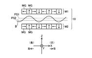
- FIG. 3 shows a side view of an undulator 10 that can be used as the undulator 1.
- the undulator 10 includes magnet rows M1 and M2 arranged in parallel with a gap so as to face each other.
- FIG. 3 is a side view of the magnet arrays M1 and M2 constituting the undulator 10 when viewed along a direction parallel to the Y axis.
- the magnet row M1 is arranged on the upper side with respect to the magnet row M2.
- Each of the magnet row M1 and the magnet row M2 is formed by a plurality of magnets MG arranged in a straight line.
- Each magnet MG is formed of a permanent magnet such as a neodymium magnet.
- the arrows marked in each magnet MG indicate the magnetization direction of each magnet MG (the direction from the S pole to the N pole) (the same applies to FIGS. 4A and 4B described later). ).
- the magnetization direction of the plurality of magnets MG included in the magnet array M1 and the magnetization direction of the plurality of magnets MG included in the magnet array M2 periodically change along the X-axis direction, and based on the periodic change, the magnet array A periodic magnetic field B is formed between M1 and M2.
- the periodic magnetic field B the direction and magnitude of the magnetic field component perpendicular to the X axis change periodically, and the period corresponds to the above-described magnetic field period ⁇ u.
- the interval between the magnet arrays M1 and M2 is referred to as the magnetic pole interval. If this magnetic pole interval is set appropriately, two paths PS1 and PS2 separated from each other can be secured in the space between the magnet arrays M1 and M2.
- the path PS1 is a path of the first electron beam in the undulator 10 that is a part of the electron beam path 8A shown in FIG.
- the path PS2 is a path of the second electron beam in the undulator 10 that is a part of the electron beam path 8B shown in FIG.
- the passages PS1 and PS2 are separated along the Z-axis direction. However, as long as the passages PS1 and PS2 are separated from each other, their positional relationship is arbitrary. For example, the passages PS1 and PS2 May be separated along the Y-axis direction.
- the magnet array M1 since the magnet array M1 is arranged on the upper side with respect to the magnet array M2, in the periodic magnetic field B, the direction and magnitude of the Z-axis component of the magnetic field periodically change.
- the positional relationship between the magnet array M1 and the magnet array M2 is arbitrary as long as the direction and magnitude of the magnetic field component perpendicular to the X axis changes periodically.
- the magnetic pole spacing between the magnet arrays M1 and M2 The magnet arrays M1 and M2 may be arranged side by side so that the direction of is parallel to the Y axis.
- Halbach type magnet arrays in which four magnets MG are arranged in one cycle are illustrated as the magnet arrays M1 and M2, but any type of magnet array that can constitute the periodic magnetic field B is illustrated. It may be used as the magnet arrays M1 and M2 (the same applies to the second embodiment described later).
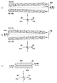
- FIG. 4A and 4B are side views of the undulator portions 20A and 20B according to the second embodiment. It can be used as the undulator 20 (see FIG. 4C) including the undulator portions 20 ⁇ / b> A and 20 ⁇ / b> B.
- Each of the undulator portions 20A and 20B includes magnet arrays M1 and M2 arranged at intervals so as to face each other, and has a self-amplifying spontaneous emission function, like the undulator 10 of FIG.
- FIG. 4A shows a side view of the magnet arrays M1 and M2 constituting the undulator unit 20A when viewed along a direction parallel to the Y axis.
- FIG. 4B shows a side view of the magnet arrays M1 and M2 constituting the undulator unit 20B when viewed along a direction parallel to the Y axis.
- the undulator portions 20A and 20B are arranged side by side in the Y-axis direction.
- each of the undulator portions 20A and 20B the configuration of the magnet arrays M1 and M2 is the same as that described in the first embodiment. Therefore, in each of the undulator portions 20A and 20B, the magnetization directions of the plurality of magnets MG included in the magnet array M1 and the magnetization directions of the plurality of magnets MG included in the magnet array M2 change periodically along the X-axis direction. Based on the periodic change, a periodic magnetic field is formed between the magnet arrays M1 and M2. In each periodic magnetic field, the direction and magnitude of the magnetic field component perpendicular to the X axis change periodically, and the period corresponds to the above-described magnetic field period ⁇ u.
- the space between the magnet rows M1 and M2 in which the periodic magnetic field of the undulator unit 20A is formed is referred to as a path space PSa
- the space in which the periodic magnetic field of the undulator unit 20B is formed is called a path space PSb.
- the path spaces PSa and PSb are two spaces separated from each other.
- the path space PSa serves as a path for the first electron beam that travels in the positive direction of the X axis in the undulator portion 20A, and the path space PSb travels in the negative direction of the X axis in the undulator portion 20B. It becomes a path for two electron beams. That is, when the undulator 20 is used as the undulator 1, the path space PSa functions as an electron beam path in the undulator 1 that is a part of the electron beam path 8A shown in FIG. 2B functions as an electron beam path in the undulator 1, which is a part of the electron beam path 8B shown in FIG.
- the first electron beam travels in the right direction (that is, the positive direction of the X axis) in the path space PSa, and the second electron beam travels in the left direction (that is, in the negative direction of the X axis) in the path space PSb.
- the path space PSa has a taper that expands in the traveling direction of the first electron beam (that is, in the right direction), and the path space PSb extends in the traveling direction of the second electron beam.
- it has a taper that spreads out (ie, toward the left).
- the magnetic pole spacing between the magnet arrays M1 and M2 increases as it goes to the right, that is, the cross-sectional area of the path space PSa increases as it goes to the right.
- the magnet rows M1 and M2 of the undulator section 20A are arranged so as to be inclined with respect to the magnet rows M1 and M2 of the undulator 10.
- the magnet arrays M1 and M2 are arranged in a plane parallel to the Z axis and the X axis so that the magnetic pole spacing, which is the distance in the Z axis direction, increases toward the right. It is arranged at an angle.
- the undulator 10 of FIG. 3 is configured such that the magnetic pole spacing between the magnet arrays M1 and M2 increases toward the left, that is, the cross-sectional area of the path space PSb increases toward the left.
- the magnet rows M1 and M2 of the undulator section 20B are arranged so as to be inclined with respect to the magnet rows M1 and M2.
- the magnet arrays M1 and M2 are arranged in a plane parallel to the Z axis and the X axis so that the magnetic pole interval, which is the interval in the Z axis direction, increases toward the left. It is arranged at an angle.
- the cross-sectional area refers to an area in a cross section orthogonal to the X axis (that is, a cross section orthogonal to the traveling direction of the electron beam).
- the taper As described above, a stronger interaction appears between the light generated by the synchrotron radiation generated by the meandering traveling of the first electron beam and the first electron beam in the undulator portion 20A, and self-amplification occurs. Increasing and stronger laser radiation is obtained.
- the undulator unit 20A and the undulator unit 20B may have the same configuration except that the taper spreading direction is different.
- the undulator portions 20A and 20B are arranged side by side in the Y-axis direction. Therefore, for example, the Z-axis coordinate value of the traveling axis of the first electron beam and the second electron beam Both the Z-axis coordinate values of the traveling axes may be zero, but the Z-axis coordinate values may be slightly different from each other (that is, the traveling axes of the first and second electron beams are viewed from the side. Sometimes, the travel axes may be completely overlapped or may be slightly deviated from each other).
- column M1 is arrange
- the direction and magnitude of the Z-axis component of the magnetic field periodically change.
- the direction and magnitude of the magnetic field component perpendicular to the X-axis change periodically.
- the positional relationship between the magnet array M1 and the magnet array M2 is arbitrary.
- the magnet arrays M1 and M2 may be arranged side by side so that the direction of the magnetic pole spacing of the magnet arrays M1 and M2 is parallel to the Y axis.
- the positional relationship between the undulator units 20A and 20B is arbitrary, and the undulator 20 It is sufficient that the undulator portions 20A and 20B are arranged in parallel in two stages.
- the undulator portions 20A and 20B may be arranged in two upper and lower stages.
- the undulator 20 is a device that separates the path spaces of the periodic magnetic fields for the first and second electron beams, but shares the arrangement space of the entire undulator device including those path spaces.
- the undulator unit 20A and 20B may be supported and integrated by a common mount (not shown).
- a left system composed of a device group disposed on the left side of the undulator 1
- a right system composed of a device group disposed on the right side of the undulator 1.
- the arrangement positions of the deflection magnet 2A, the superconducting linac 3A, the distribution magnet 4A, the electron gun 5A, and the beam dump 6A are the arrangement positions of the deflection magnet 2B, the superconducting linac 3B, the distribution magnet 4B, the electron gun 5B, and the beam dump 6B, respectively.
- the left system and the right system described above may be arranged in a rotationally symmetric relationship with respect to the center of the undulator 1. That is, the arrangement positions of the deflection magnet 2A, the superconducting linac 3A, the distribution magnet 4A, the electron gun 5A, and the beam dump 6A are the arrangement positions of the deflection magnet 2B, the superconducting linac 3B, the distribution magnet 4B, the electron gun 5B, and the beam dump 6B, respectively.
- the arrangement relationship may be changed from that shown in FIG. 1 so as to have a point-symmetric relationship about the center of the undulator 1.
- an FEL system including a plurality of bidirectional FELs 100 may be constructed.
- a plurality of bidirectional FELs 100 are arranged side by side along the Y-axis direction.
- the laser beam directed to the right is derived from the light beam line 7B
- the laser beam directed to the left is derived from the light beam line 7A. Therefore, for example, if three bidirectional FELs 100 are arranged, a total of six light beam lines can be obtained.
- the FEL system is suitable for mass production exposure.
Landscapes
- Physics & Mathematics (AREA)
- Engineering & Computer Science (AREA)
- Plasma & Fusion (AREA)
- Spectroscopy & Molecular Physics (AREA)
- Electromagnetism (AREA)
- Optics & Photonics (AREA)
- Lasers (AREA)
- Particle Accelerators (AREA)
Abstract
自己増幅自発放射機能を持つアンジュレータ(1)の両側に2台の超電導リニアック(3A、3B)を1台ずつ配置する。2台の超電導リニアック(3A、3B)は、夫々において加速した電子ビームをアンジュレータ(1)に対して互いに逆方向から入射し(8A、8B)、これによってアンジュレータ1の両側からレーザー放射光を得る(7B、7A)。一方の超電導リニアック(3B、3A)は、他方の超電導リニアック(3A、3B)から入射されてアンジュレータ(1)から出射された電子ビームに対しエネルギー回収のための減速を行う。
Description
本発明は、双方向自由電子レーザー装置に関する。
極端紫外線領域からX線領域に至る短波長放射光の利用が注目されている。特に半導体デバイスの分野においては、集積回路の高密度化が露光技術に依存しており、10nm(ナノメートル)以下の線幅を実現するには、13.5nmの波長を有する極端紫外光が必須と言われている。しかしながら、このような短波長の極端紫外光を大量生産露光に必要な強度を持って照射できる現実的な光源はこれまでになく、高繰り返しの自由電子レーザー装置に可能性が委ねられている。
峰原英介、"原研超電導リニアック駆動自由電子レーザー 極短パルス、高効率、高出力、波長可変レーザーの実現に向けて(The JAERI Free-Electron Laser Driven by a Superconducting rf Linac. Towards Ultra-Short Pulse, Highly-Efficient, High Power, and Tunable Coherent Light Sources)"、放射光、日本放射光学会(The Japanese Society for Synchrotron Radiation Research)、2001年、第14巻、第3号(2001)、 p.182-189
特許文献1、2及び3には、レーザー光に対する光共振器を有する構成の自由電子レーザー装置(以下、FELと称することがある)が開示されているが、13.5nmでは光共振器を構成しうる高効率反射鏡は存在しないため、十分な放射光の強度が得られず、光共振器を使うFELを極端紫外光源として利用することは困難である。この短波長領域で大量生産露光に必要とされる1kW(キロワット)レベルの光強度を得るためには、長いアンジュレータを用いた自己増幅自発放射(Self-Amplified Spontaneous Emission)型の自由電子レーザー装置であって且つ高繰り返しのものが必須であり、そのためには例えば、特許文献3及び非特許文献1と同様に超電導リニアックを利用した駆動が望ましい。
一方で、エネルギー効率等を考慮すれば、利用済電子ビームが持つエネルギーを回収することも肝要である。しかしながら、特許文献3及び非特許文献1に記されたようなエネルギーを回収するために電子ビームを反転させる方式においては、反転を担うための反転アーク部(ループ電子路)が必須となる。これは、装置設置面積の増大要因及び施設の面積利用効率の低下要因となりえる。特に例えば、13.5nmのレーザー光を生成する程度に電子ビームエネルギーが高い場合においては、レーザー光を生成する部分を自己増幅自発放射型で構成した場合であっても、反転アーク部(ループ電子路)の半径が相当に大きくなるため、施設の面積利用効率が相当に悪くなる。装置設置面積の増大、施設の面積利用効率の低下が望ましくないことは言うまでも無い。
尚、説明の具体化のため、13.5nmの波長を有する極端紫外光に注目して従来のFELの構成等を説明したが、13.5nm以外の波長を有するレーザー光を得ようとした場合にも同様のことが言える。
そこで本発明は、面積利用効率の向上等に寄与しつつ高いエネルギー効率で高強度のレーザー放射光(特に例えば極端紫外線領域の短波長のレーザー放射光)を出射し得る双方向自由電子レーザー装置を提供することを目的とする。
本発明に係る一側面に係る双方向自由電子レーザー装置は、自己増幅自発放射機能を持つアンジュレータを用いて双方向にレーザー放射光を得る双方向自由電子レーザー装置であって、前記アンジュレータの両側に1台ずつ配置され、各々に前記アンジュレータに対し電子ビームを入射する2台の超電導リニアックを備え、前記アンジュレータの一方の端部から入射し他方の端部から出射する電子ビームに対し、加速とエネルギー回収のための減速とを前記2台の超電導リニアックで分担して行うことを特徴とする。
本発明に係る他の側面に係る双方向自由電子レーザー装置は、自己増幅自発放射機能を持つアンジュレータと、前記アンジュレータを挟んで配置され、各々に電子ビームに対する加速と減速の機能を有する2台の超電導リニアックと、前記2台の超電導リニアックに対し電子ビームを供給する2台の電子銃と、を備え、各電子銃から一方の超電導リニアックと前記アンジュレータと他方の超電導リニアックとを通る電子ビーム通路を構成することで、電子ビームの走行方向が互いに逆の2本の電子ビーム通路を構成するとともに前記アンジュレータの両側からレーザー放射光を得ることを特徴とする。
本発明によれば、面積利用効率の向上等に寄与しつつ高いエネルギー効率で高強度のレーザー放射光(特に例えば極端紫外線領域の短波長のレーザー放射光)を出射し得る双方向自由電子レーザー装置を提供することが可能となる。
以下、本発明の実施形態の例を、図面を参照して具体的に説明する。参照される各図において、同一の部分には同一の符号を付し、同一の部分に関する重複する説明を原則として省略する。
本発明においては、自由電子を媒体とした自己増幅自発放射(Self-Amplified Spontaneous Emission)機構をアンジュレータと呼び、電子の線形加速器をリニアック(Linac)と略称する。
[基本構成の説明]
図1は、本発明の実施形態に係る双方向自由電子レーザー装置(以下、双方向FELと称する)100の概略構成図である。図1では、双方向FEL100の各構成装置を上方から見たときの、各構成装置の概略外形が示されている。
図1は、本発明の実施形態に係る双方向自由電子レーザー装置(以下、双方向FELと称する)100の概略構成図である。図1では、双方向FEL100の各構成装置を上方から見たときの、各構成装置の概略外形が示されている。
双方向FEL100は、アンジュレータ1と、偏向磁石2A及び2Bと、超電導リニアック3A及び3Bと、振り分け磁石4A及び4Bと、電子銃5A及び5Bと、ビームダンプ6A及び6Bと、光ビームライン7A及び7Bと、を備えて構成される。偏向磁石2A及び2Bは互いに同じ構成を有していて良い。超電導リニアック3A及び3Bは互いに同じ構成を有していて良い。振り分け磁石4A及び4Bは互いに同じ構成を有していて良い。電子銃5A及び5Bは互いに同じ構成を有していて良い。ビームダンプ6A及び6Bは互いに同じ構成を有していて良い。光ビームライン7A及び7Bは互いに同じ構成を有していて良い。
図2(a)に、電子銃5Aから出射された第1電子ビームの通路である電子ビーム通路8Aを示す。電子ビーム通路8Aは、電子銃5Aから、振り分け磁石4A、超電導リニアック3A、偏向磁石2A、アンジュレータ1、偏向磁石2B、超電導リニアック3B、振り分け磁石4Bを、この順番で経由してビームダンプ6Bに至る通路である。
図2(b)に、電子銃5Bから出射された第2電子ビームの通路である電子ビーム通路8Bを示す。電子ビーム通路8Bは、電子銃5Bから、振り分け磁石4B、超電導リニアック3B、偏向磁石2B、アンジュレータ1、偏向磁石2A、超電導リニアック3A、振り分け磁石4Aを、この順番で経由してビームダンプ6Aに至る通路である。
図2(b)に、電子銃5Bから出射された第2電子ビームの通路である電子ビーム通路8Bを示す。電子ビーム通路8Bは、電子銃5Bから、振り分け磁石4B、超電導リニアック3B、偏向磁石2B、アンジュレータ1、偏向磁石2A、超電導リニアック3A、振り分け磁石4Aを、この順番で経由してビームダンプ6Aに至る通路である。
以下では、説明の具体化及び明確化のため、双方向FEL100が設置される実空間内に、互いに直交するX軸、Y軸及びZ軸を定義する。X軸及びY軸は水平面に平行であって、Z軸は鉛直面に平行であるとする。アンジュレータ1の長さ方向、即ち、アンジュレータ1内を走行する電子ビームの走行方向はX軸に平行である。更に、アンジュレータ1の中心にX軸の原点をとり、偏向磁石2A、超電導リニアック3A、振り分け磁石4A、電子銃5A、ビームダンプ6A及び光ビームライン7AがX軸の負側に設置され、且つ、偏向磁石2B、超電導リニアック3B、振り分け磁石4B、電子銃5B、ビームダンプ6B及び光ビームライン7BがX軸の正側に設置されているものとする。また、アンジュレータ1の中心からX軸の正側に向かう向きを右と定義し、アンジュレータ1の中心からX軸の負側に向かう向きを左と定義する。
記号1a、1bは、夫々、アンジュレータ1の長さ方向における一方の端部、他方の端部を表す。アンジュレータ1において、端部1aから端部1bに向かう方向は、X軸に並行であってX軸の負側から正側に向かう方向と一致する。記号3Aa、3Abは、超電導リニアック3Aにおける一方の端部、他方の端部を表す。記号3Ba、3Bbは、超電導リニアック3Bにおける一方の端部、他方の端部を表す。アンジュレータ1と同様、超電導リニアック3A及び3Bの夫々において、長さ方向は、電子ビームの走行方向と一致する。超電導リニアック3Aにおいて、端部3Aaから端部3Abに向かう方向は、X軸から傾いているが、X軸の負側から正側に向かう成分を有する。超電導リニアック3Bにおいて、端部3Baから端部3Bbに向かう方向は、X軸から傾いているが、X軸の正側から負側に向かう成分を有する。
図1及び図2(a)及び(b)に示すように、双方向FEL100では、長尺且つ共通のアンジュレータ1を挟むようにアンジュレータ1の両側に超電導リニアック3A、3Bを配置し、それらで加速された電子ビームを偏向磁石2A、2Bで軌道を変えて共通のアンジュレータ1に互いに逆方向から導くことで、自己増幅自発放射機構によるレーザー放射光(即ち、放射光に基づくレザー光)を発生させるものである。超電導リニアック3Aで加速された電子ビームに基づくレーザー放射光は光ビームライン7Bに導かれ、超電導リニアック3Bで加速された電子ビームに基づくレーザー放射光は光ビームライン7Aに導かれる。双方向FEL100にて発生するレーザー放射光は、短波長の自由電子レーザー光であって良い。ここにおける短波長とは、例えば、極端紫外線領域に属する波長からX線領域に属する波長までの波長を指し、例えば、1nmから数10nmまでの範囲内の波長を指す。
電子銃5A、5Bで生成された電子ビームは、振り分け磁石4A、4Bで軌道を曲げられて超電導リニアック3A、3Bに導かれ、超電導リニアック3A、3Bにて加速された電子ビームは、偏向磁石2A、2Bにて軌道を再度曲げられてからアンジュレータ1に投入(即ち入射)される。
電子銃5Aからの電子ビームに基づきアンジュレータ1にてレーザー光を放出した電子は、偏向磁石2Bを通じて超電導リニアック3Bに導かれ、超電導リニアック3Bの中を超電導リニアック3Bで加速される電子とは逆方向に走行することで減速された後、再び振り分け磁石4Bで軌道を曲げられてビームダンプ6Bに導かれる。
電子銃5Bからの電子ビームに基づきアンジュレータ1にてレーザー光を放出した電子は、偏向磁石2Aを通じて超電導リニアック3Aに導かれ、超電導リニアック3Aの中を超電導リニアック3Aで加速される電子とは逆方向に走行することで減速された後、再び振り分け磁石4Aで軌道を曲げられてビームダンプ6Aに導かれる。
電子銃5Bからの電子ビームに基づきアンジュレータ1にてレーザー光を放出した電子は、偏向磁石2Aを通じて超電導リニアック3Aに導かれ、超電導リニアック3Aの中を超電導リニアック3Aで加速される電子とは逆方向に走行することで減速された後、再び振り分け磁石4Aで軌道を曲げられてビームダンプ6Aに導かれる。
電子の減速時に回収されたエネルギーを、各超電導リニアックにおいて、正方向に走行する電子の加速用エネルギーとして利用することができる。また、各超電導リニアックを負方向に走行する間に電子ビームは十分に減速されるので、ビームダンプ6A、6Bでの放射線的問題を回避することができる。即ち、各ビームダンプで発生しうる放射線の強度を低く抑えることができ、放射線の遮蔽対策レベルを低く抑えることができる。尚、超電導リニアック3A、3Bの夫々において、電子が加速される方向を正方向と称し、その逆方向を負方向と称する。超電導リニアック3Aにおいては、端部3Aaから端部3Abに向かう方向が正方向であり、超電導リニアック3Bにおいては、端部3Baから端部3Bbに向かう方向が正方向である。
[動作原理の説明]
本実施形態に係る双方向FEL100は、基本的には、アンジュレータ機能としての自己増幅自発放射機構を利用する短波長自由電子レーザー装置を二基組み合わせた上で、長尺アンジュレータを共通にしたものである。また、大出力を得るために、熱損失が無く繰り返しの高い超電導リニアック1対を用いて双方向電子の加速と減速を並行して行うものである。
本実施形態に係る双方向FEL100は、基本的には、アンジュレータ機能としての自己増幅自発放射機構を利用する短波長自由電子レーザー装置を二基組み合わせた上で、長尺アンジュレータを共通にしたものである。また、大出力を得るために、熱損失が無く繰り返しの高い超電導リニアック1対を用いて双方向電子の加速と減速を並行して行うものである。
短波長自由電子レーザー光を発生させるためには、高エネルギー電子加速が必要となる。半導体分野の高細密露光に必要な13.5nmの極端紫外線を実用可能な強度で発生させる場合、電子を約280MeV(メガエレクトロンボルト)程度まで加速する必要がある。このような電子の加速を最小のエネルギー損失で実現するために用いる超電導リニアック3A、3Bとして、例えば1m(メートル)当たり20MeVの割合で加速が行われるよう、1.3GHz(ギガヘルツ)で励振する全長15mほどの直進型多空洞共振器を用いると良い。この直進型多空洞共振器は超電導材料で構成され、冷凍機からの超低温液に浸漬された状態で動作するので、電気抵抗による損失は略ゼロとなる。尚、本発明において使用する2台の超電導リニアック3A、3Bでは、夫々にその中に2本の電子ビーム通路を必要とするが、この点に特別の技術的制約はなく、既に知られた技術で構成することができる(各超電導リニアックにおいて、単一の直進型多空洞共振器内に、正方向に走行する電子ビーム用の通路と負方向に走行する電子ビーム用の通路とを、互いに分離して確保すれば足る)。
レーザー放射光は、アンジュレータ1の中を加速電子がシンクロトロン走行する際の自己増幅自発放射機構により得られるが、放射光の波長は基本的にアンジュレータ1内の電子ビーム通路における磁界周期に比例する。例えば、13.5nmの極端紫外線を放射光として得ようとした場合、その磁界周期は20mm(ミリメートル)程度となる。また、アンジュレータ1の長さは、主として導入される電子のエネルギーに依存するものとされており、極端紫外線領域の放射光を得る場合、アンジュレータ1に入るときの電子エネルギーが前述の280MeV程度であれば、アンジュレータ1の長さは10~20mの範囲内の長さで十分である。
ここで、一般に、FELにおける放射光の波長λLは、例えば非特許文献1にも記載されているように、正確には以下の数式(1)で定まる。
λL=λu/2γ2 ・(1+K/2) …(1)
λuはアンジュレータ内の電子ビーム通路における磁界周期を表し、γはアンジュレータに入射される電子ビームの電子エネルギーを表し、Kはアンジュレータでの磁界強度や磁界周期で定まる係数を表す。
λL=λu/2γ2 ・(1+K/2) …(1)
λuはアンジュレータ内の電子ビーム通路における磁界周期を表し、γはアンジュレータに入射される電子ビームの電子エネルギーを表し、Kはアンジュレータでの磁界強度や磁界周期で定まる係数を表す。
故に、本実施形態に係る双方向FEL100により、波長13.5nmで1kWレベルの強度を持った極端紫外線の放射光を得るためには、先に例示したような280MeVの電子エネルギーと、20mm程の磁界周期を有する長さ20m程度のアンジュレータ1が必要となり、その場合の係数Kの値は1.5程度になる。
また、アンジュレータ1の中にも電子ビームの双方向通路を必要とするが、この点に関しては、例えば、周期磁場を形成する磁極間隔を若干広げるだけで2本の通路を容易に確保することができる。従って、このアンジュレータ1自体も公知の技術を利用して組み立てることができ、その構成自体に特別の工夫は必要としない。
但し、後述するように、アンジュレータ1内での電子と放射光との相互作用による自己増幅機能がより高まるよう、電子ビームの走行空間にテーパを設ける場合には、双方向の電子通路を互いに分離する必要がある。従って、超電導リニアック3Aから入射する第1電子ビームと超電導リニアック3Bから入射する第2電子ビームに対して共通に利用されるアンジュレータ1は、第1及び第2電子ビームに対する周期磁場通路空間を共通とした1基のアンジュレータを必ずしも意味しておらず、第1及び第2電子ビームに対する周期磁場通路空間を分離しつつも、それらの配置スペースを共通化した構成も当然含むものである。
ところで一般に大出力のFELにおいては、レーザー光放出後に大量の高エネルギー電子を処理する必要が生ずる。先に説明したように特許文献3等の従来のエネルギー回収型リニアックでは、ループ状の電子の反転アーク部(特許文献3では図1の構成要素5に相当)を設けることによって単一の超電導リニアックで加速と減速を行い、利用済電子ビームは位相を異ならせて減速させることにより廃棄に伴う放射線対策としている。しかしながら、実際の産業分野で利用可能な装置構成の面からは、必要強度のレーザー光を得ようとすると、相応に高いエネルギーの電子が必須となるため、必然的に反転アーク部も大きくなり、装置全体の設置面積が大きくなると共に施設の面積利用効率が低下する(ループ状の反転アーク部の内側が無駄なスペースとなる)。
この点、本実施形態に係る双方向FEL100においては、対向する側の超電導リニアックの逆方向減速電界を利用して利用済電子ビームを減速し、減速時に回収されるエネルギーを正方向電子ビームの加速に用いることによって、エネルギー効率を高めている。即ち、本実施形態では、反転アーク部ではなく、独立した二基の超電導リニアック3A、3Bを互いに加速、減速に用いると言う新しい発想に基づいて、双方向FEL100を構成しているので、装置全体の設置面積を小さくすることができると共に、面積利用効率を大幅に向上させることができる。また、上記の如く利用済電子ビームを減速することで、利用済の高エネルギー電子に対する放射線遮蔽対策を軽減することができる。
因みに、先に述べたように例えばアンジュレータ1の長さを20mとすると共に、超電導リニアック3A、3Bを中心とした加速系の長さをそれぞれ15mとすれば、双方向FEL100は、全体として、50m×10m四方、即ち500m2の工場建屋に収まるものとなる。この大きさは、特許文献1や特許文献3に開示されたような電子ビームの反転アーク部(ループ電子路)を必要とする従来施設に比べ、面積比で1/5以下のものとなり、工場設備として極めて現実的なものと言うことができる。その上、放射光のビームラインが2本同時に得られるので、施設の面積利用効率は更に2倍に高まることになる。つまり、本発明に係る双方向FEL100によれば、所望強度の短波長放射光を得るに当たり、特許文献1等の従来FELと比べ、全体として10倍の面積利用効率を達成でき、コストも格段に低廉化できる。本発明は、特に半導体デバイスの分野において、露光技術の高細密化に寄与し且つ製造効率の向上に寄与すると考えられる。
上述した双方向FEL100の構成及び動作等を、便宜上、基本構成例と称する。以下、複数の実施例の中で、双方向FEL100のより詳細な構成や、応用技術、変形技術等を説明する。特に記述無き限り且つ矛盾無き限り、基本構成例について説明した上述の全ての事項が後述の各実施例に適用され、各実施例において基本構成例と矛盾する事項については、各実施例での記載が優先される。また矛盾無き限り、以下に述べる複数の実施例の内、任意の実施例に記載した事項を、他の任意の実施例に適用することもできる(即ち複数の実施例の内の任意の2以上の実施例を組み合わせることも可能である)。
[第1実施例]
第1実施例を説明する。第1実施例において、双方向FEL100の構成及び動作の詳細な一例を説明する。既に述べた事項から明らかであるが、双方向FEL100は、アンジュレータ1の左側に配置された装置群から成る左系統(第1加速系統)と、アンジュレータ1の右側に配置された装置群から成る右系統(第2加速系統)と、左系統と右系統に共用される共通アンジュレータとも称されるべきアンジュレータ1と、を備えて構成される。
第1実施例を説明する。第1実施例において、双方向FEL100の構成及び動作の詳細な一例を説明する。既に述べた事項から明らかであるが、双方向FEL100は、アンジュレータ1の左側に配置された装置群から成る左系統(第1加速系統)と、アンジュレータ1の右側に配置された装置群から成る右系統(第2加速系統)と、左系統と右系統に共用される共通アンジュレータとも称されるべきアンジュレータ1と、を備えて構成される。
左系統の電子銃5Aは、第1電子ビームを生成して出射する。例えば、電子銃5Aで生成された第1電子流は、繰り返し周波数1GHz(ギガヘルツ)程度で断続する第1電子ビームとして電子銃5Aから打ち出される。電子銃5Aから出射された第1電子ビームは、図示しない初段加速度で所定の初速度を与えられた後、振り分け磁石4Aに入射する。
振り分け磁石4Aは、電子銃5Aからの第1電子ビームの軌道を曲げることで第1電子ビームを超電導リニアック3Aの端部3Aaに導き、これによって第1電子ビームが超電導リニアック3Aに投入(即ち入射)される。
超電導リニアック3Aは、電子銃5Aから振り分け磁石4Aを経由して入射された第1電子ビームを加速して、加速された第1電子ビームを超電導リニアック3Aの端部3Abから出射する。第1電子ビームは、超電導リニアック3A内を走行する間に280MeV程度のエネルギーを持つまで加速される。
振り分け磁石2Aは、超電導リニアック3Aの他端3Abから出射された第1電子ビームの軌道を曲げることで第1電子ビームをアンジュレータの端部1aに導き、これによって、超電導リニアック3Aにて加速された第1電子ビームが端部1aからアンジュレータ1に投入(即ち入射)される。
振り分け磁石4Aは、電子銃5Aからの第1電子ビームの軌道を曲げることで第1電子ビームを超電導リニアック3Aの端部3Aaに導き、これによって第1電子ビームが超電導リニアック3Aに投入(即ち入射)される。
超電導リニアック3Aは、電子銃5Aから振り分け磁石4Aを経由して入射された第1電子ビームを加速して、加速された第1電子ビームを超電導リニアック3Aの端部3Abから出射する。第1電子ビームは、超電導リニアック3A内を走行する間に280MeV程度のエネルギーを持つまで加速される。
振り分け磁石2Aは、超電導リニアック3Aの他端3Abから出射された第1電子ビームの軌道を曲げることで第1電子ビームをアンジュレータの端部1aに導き、これによって、超電導リニアック3Aにて加速された第1電子ビームが端部1aからアンジュレータ1に投入(即ち入射)される。
アンジュレータ1に投入された第1電子ビームは、アンジュレータ1が形成する周期磁場によってシンクロトロン放射に寄与しながら右方向(即ちX軸の正の方向)に走行して端部1bから出射される。第1電子ビームに基づくシンクロトロン放射による放射光は第1レーザー光(換言すれば第1レーザー放射光)として光ビームライン7Bに導出され、そのまま又は必要な光増幅器(不図示)を通じて利用に供される。
アンジュレータ1の端部1bから出射された第1電子ビームは、偏向磁石2Bによって軌道を曲げられて超電導リニアック3Bの端部3Bbに導かれる。これによってアンジュレータ1内を走行後の第1電子ビームは、超電導リニアック3Bに投入(即ち入射)されて超電導リニアック3B内を端部3Bbから端部3Baに向けて走行し、その後、振り分け磁石4Bを経由してビームダンプ6Bに捨てられる。
超電導リニアック3B内には、正方向(即ち端部3Baから端部3Bbに向かう方向)に走行する第2電子ビームを加速させるための電界が存在し、その電界は、負方向に走行する第1電子ビームに対しては逆の作用を及ぼすため、第1電子ビームは、超電導リニアック3B内を走行する間に十分に減速せしめられる。超電導リニアック3Bは、第1電子ビームの減速分のエネルギーを回収し、回収したエネルギーを、正方向に走行する第2電ビームを加速させるためのエネルギーとして再利用する。このようなエネルギーの回収方法及び再利用方法として公知の方法を用いることができる。
右系統の電子銃5Bは、第2電子ビームを生成して出射する。例えば、電子銃5Bで生成された第2電子流は、繰り返し周波数1GHz(ギガヘルツ)程度で断続する第2電子ビームとして電子銃5Bから打ち出される。電子銃5Bから出射された第2電子ビームは、図示しない初段加速度で所定の初速度を与えられた後、振り分け磁石4Bに入射する。
振り分け磁石4Bは、電子銃5Bからの第2電子ビームの軌道を曲げることで第2電子ビームを超電導リニアック3Bの端部3Baに導き、これによって第2電子ビームが超電導リニアック3Bに投入(即ち入射)される。
超電導リニアック3Bは、電子銃5Bから振り分け磁石4Bを経由して入射された第2電子ビームを加速して、加速された第2電子ビームを超電導リニアック3Bの端部3Bbから出射する。第2電子ビームは、超電導リニアック3B内を走行する間に280MeV程度のエネルギーを持つまで加速される。
振り分け磁石2Bは、超電導リニアック3Bの他端3Bbから出射された第2電子ビームの軌道を曲げることで第2電子ビームをアンジュレータの端部1bに導き、これによって、超電導リニアック3Bにて加速された第2電子ビームが端部1bからアンジュレータ1に投入(即ち入射)される。
振り分け磁石4Bは、電子銃5Bからの第2電子ビームの軌道を曲げることで第2電子ビームを超電導リニアック3Bの端部3Baに導き、これによって第2電子ビームが超電導リニアック3Bに投入(即ち入射)される。
超電導リニアック3Bは、電子銃5Bから振り分け磁石4Bを経由して入射された第2電子ビームを加速して、加速された第2電子ビームを超電導リニアック3Bの端部3Bbから出射する。第2電子ビームは、超電導リニアック3B内を走行する間に280MeV程度のエネルギーを持つまで加速される。
振り分け磁石2Bは、超電導リニアック3Bの他端3Bbから出射された第2電子ビームの軌道を曲げることで第2電子ビームをアンジュレータの端部1bに導き、これによって、超電導リニアック3Bにて加速された第2電子ビームが端部1bからアンジュレータ1に投入(即ち入射)される。
アンジュレータ1に投入された第2電子ビームは、アンジュレータ1が形成する周期磁場によってシンクロトロン放射に寄与しながら左方向(即ちX軸の負の方向)に走行して端部1aから出射される。第2電子ビームに基づくシンクロトロン放射による放射光は第2レーザー光(換言すれば第2レーザー放射光)として光ビームライン7Aに導出され、そのまま又は必要な光増幅器(不図示)を通じて利用に供される。
アンジュレータ1の端部1aから出射された第2電子ビームは、偏向磁石2Aによって軌道を曲げられて超電導リニアック3Aの端部3Abに導かれる。これによってアンジュレータ1内を走行後の第2電子ビームは、超電導リニアック3Aに投入(即ち入射)されて超電導リニアック3A内を端部3Abから端部3Aaに向けて走行し、その後、振り分け磁石4Aを経由してビームダンプ6Aに捨てられる。
超電導リニアック3A内には、正方向(即ち端部3Aaから端部3Abに向かう方向)に走行する第1電子ビームを加速させるための電界が存在し、その電界は、負方向に走行する第2電子ビームに対しては逆の作用を及ぼすため、第2電子ビームは、超電導リニアック3A内を走行する間に十分に減速せしめられる。超電導リニアック3Aは、第2電子ビームの減速分のエネルギーを回収し、回収したエネルギーを、正方向に走行する第1電ビームを加速させるためのエネルギーとして再利用する。このようなエネルギーの回収方法及び再利用方法として公知の方法を用いることができる。
光ビームライン7B及び7Aに導出される各レーザー光は、高調波を含んでおり、基本構成例の説明文中で示した数値例にて双方向FEL100を構成した場合においては、それらの第5高調波が13.5nmの波長を有することとなる。従って、13.5nmのレーザー光を利用して高精細露光を行う場合には、光ビームライン7B及び7Aに導出される各レーザー光の第5高調波を選択して利用することになる。
アンジュレータ1は、上述したように、自己増幅自発放射機能を有する。即ち、特に外部から電力を加えることなく、自身に入射された電子ビームに基づき放射光を自ら発生させる自発放射機能と、光共振器を利用することなく、発生させた放射光の強度を自ら増幅する自己増幅機能と、を有している。即ち、第1電子ビームに注目して考えた場合、アンジュレータ1は、アンジュレータ1内の周期磁場と第1電子ビームに基づくシンクロトロン放射により光を発生させ(自発放射)、その発生させた光で、第1電子ビームを構成する電子に光の波長間隔での密度変調をかけ、多数の電子から出る光の位相を揃えることで光の強度を増幅する(自己増幅)。第2電子ビームに対しても同様である。
このように、超電導リニアック3Aは、第1電子ビームを加速する加速機能を備えると共に第2電子ビームを減速する減速機能を有する一方で、超電導リニアック3Bは、第2電子ビームを加速する加速機能を備えると共に第1電子ビームを減速する減速機能を有し、超電導リニアック3A及び3Bにおいて減速分のエネルギーは回収される。つまり、アンジュレータ1の一方の端部(1a又は1b)から入射し他方の端部(1b又は1a)から出射する電子ビームに対し、加速とエネルギー回収のための減速とを2台の超電導リニアック3A及び3Bで分担して行うことになる。
図3に、アンジュレータ1として用いることが可能なアンジュレータ10の側面図を示す。アンジュレータ10は、互いに対向するように間隔をあけて平行に配置された磁石列M1及びM2を備えている。図3は、アンジュレータ10を構成する磁石列M1及びM2を、Y軸に平行な方向に沿ってみたときの、それらの側面図を表している。図3では、磁石列M1が磁石列M2に対して上側に配置されている。磁石列M1及び磁石列M2の夫々は、直線状に配列された複数の磁石MGにて形成される。各磁石MGはネオジム磁石等の永久磁石で形成される。図3において、各磁石MG内に記された矢印は、各磁石MGの磁化方向(S極からN極に向かう方向)を表している(後述の図4(a)及び(b)においても同様)。
磁石列M1に含まれる複数の磁石MGの磁化方向及び磁石列M2に含まれる複数の磁石MGの磁化方向はX軸方向に沿って周期的に変化し、その周期的な変化に基づき、磁石列M1及びM2間には周期磁場Bが形成される。周期磁場Bでは、X軸に垂直な磁場成分の向き及び大きさが周期的に変化し、その周期が上述の磁界周期λuに相当する。
磁石列M1及びM2間の間隔は磁極間隔と称される。この磁極間隔を適切に設定すれば、磁石列M1及びM2間の空間に、互いに分離した2本の通路PS1及びPS2を確保することができる。通路PS1は、図2(a)に示す電子ビーム通路8Aの一部である、アンジュレータ10内の第1電子ビームの通路である。通路PS2は、図2(b)に示す電子ビーム通路8Bの一部である、アンジュレータ10内の第2電子ビームの通路である。尚、図3では、通路PS1及びPS2がZ軸方向に沿って分離しているが、通路PS1及びPS2が互いに分離している限り、それらの位置関係は任意であり、例えば、通路PS1及びPS2がY軸方向に沿って分離していても良い。
尚、図3では、磁石列M1が磁石列M2に対して上側に配置されているため、周期磁場Bにおいては、磁場のZ軸成分の向き及び大きさが周期的に変化しているが、周期磁場Bにおいて、X軸に垂直な磁場成分の向き及び大きさが周期的に変化する限り、磁石列M1と磁石列M2の位置関係は任意であり、例えば、磁石列M1及びM2の磁極間隔の方向がY軸と平行となるように磁石列M1及びM2を横に並べても良い。
また、図3では、磁石列M1及びM2として、1周期内に4個の磁石MGを配列するHalbach型磁石列が例示されているが、周期磁場Bを構成し得る任意の型の磁石列を磁石列M1及びM2として用いて良い(後述の第2実施例についても同様)。
[第2実施例]
第2実施例を説明する。図4(a)及び(b)に、第2実施例に係るアンジュレータ部20A及び20Bの側面図を示す。アンジュレータ部20A及び20Bから成るアンジュレータ20(図4(c)参照)、アンジュレータ1として用いることができる。
第2実施例を説明する。図4(a)及び(b)に、第2実施例に係るアンジュレータ部20A及び20Bの側面図を示す。アンジュレータ部20A及び20Bから成るアンジュレータ20(図4(c)参照)、アンジュレータ1として用いることができる。
アンジュレータ部20A及び20Bの夫々は、互いに対向するように間隔をあけて配置された磁石列M1及びM2を備えていて、図3のアンジュレータ10と同じく、自己増幅自発放射機能を有している。図4(a)は、アンジュレータ部20Aを構成する磁石列M1及びM2を、Y軸に平行な方向に沿ってみたときの、それらの側面図を表している。図4(b)は、アンジュレータ部20Bを構成する磁石列M1及びM2を、Y軸に平行な方向に沿ってみたときの、それらの側面図を表している。図4(c)に示す如く、アンジュレータ部20A及び20BはY軸方向に並べて配置される。
アンジュレータ部20A及び20Bの夫々において、磁石列M1及びM2の構成自体は、第1実施例で述べたものと同様である。従って、アンジュレータ部20A及び20Bの夫々において、磁石列M1に含まれる複数の磁石MGの磁化方向及び磁石列M2に含まれる複数の磁石MGの磁化方向はX軸方向に沿って周期的に変化し、その周期的な変化に基づき磁石列M1及びM2間には周期磁場が形成される。各周期磁場では、X軸に垂直な磁場成分の向き及び大きさが周期的に変化し、その周期が上述の磁界周期λuに相当する。
アンジュレータ部20Aにおいて、磁石列M1及びM2間の空間であってアンジュレータ部20Aの周期磁場が形成されている空間をパス空間PSaと呼び、アンジュレータ部20Bにおいて、磁石列M1及びM2間の空間であってアンジュレータ部20Bの周期磁場が形成されている空間をパス空間PSbと呼ぶ。アンジュレータ部20A及び20Bが互いに横方向に並べて配置されていることからも理解されるように、パス空間PSa及びPSbは互いに分離された2つの空間である。
第2実施例においては、パス空間PSaがアンジュレータ部20A内をX軸の正方向に走行する第1電子ビームの通路となり、パス空間PSbがアンジュレータ部20B内をX軸の負方向に走行する第2電子ビームの通路となる。つまり、アンジュレータ20をアンジュレータ1として用いる場合、パス空間PSaが、図2(a)に示す電子ビーム通路8Aの一部である、アンジュレータ1内の電子ビーム通路として機能し、且つ、パス空間PSbが、図2(b)に示す電子ビーム通路8Bの一部である、アンジュレータ1内の電子ビーム通路として機能する。
第1電子ビームはパス空間PSa内を右方向(即ちX軸の正の方向)に走行し、第2電子ビームはパス空間PSb内を左方向(即ちX軸の負の方向)に走行することとなるが、パス空間PSaは、第1電子ビームの走行方向に対して(即ち右方向に向けて)広がりを持つテーパを有し、且つ、パス空間PSbは、第2電子ビームの走行方向に対して(即ち左方向に向けて)広がりを持つテーパを有する。
より具体的には、アンジュレータ部20Aにおいて、磁石列M1及びM2間の磁極間隔が右に向かうにつれて大きくなるように、即ち、パス空間PSaの断面積が右に向かうにつれて大きくなるように、図3のアンジュレータ10の磁石列M1及びM2を基準として、アンジュレータ部20Aの磁石列M1及びM2が互いに傾けて配置される。図4(a)のアンジュレータ部20Aの例では、Z軸方向の間隔である磁極間隔が右に向かうにつれて大きくなるように、Z軸及びX軸に平行な面内で磁石列M1及びM2が互いに傾けて配置されている。
同様に、アンジュレータ部20Bにおいて、磁石列M1及びM2間の磁極間隔が左に向かうにつれて大きくなるように、即ち、パス空間PSbの断面積が左に向かうにつれて大きくなるように、図3のアンジュレータ10の磁石列M1及びM2を基準として、アンジュレータ部20Bの磁石列M1及びM2が互いに傾けて配置される。図4(b)のアンジュレータ部20Bの例では、Z軸方向の間隔である磁極間隔が左に向かうにつれて大きくなるように、Z軸及びX軸に平行な面内で磁石列M1及びM2が互いに傾けて配置されている。
尚、パス空間PSa、PSbにおいて、断面積とは、X軸に直交する断面(即ち電子ビームの走行方向に直交する断面)での面積を指す。
同様に、アンジュレータ部20Bにおいて、磁石列M1及びM2間の磁極間隔が左に向かうにつれて大きくなるように、即ち、パス空間PSbの断面積が左に向かうにつれて大きくなるように、図3のアンジュレータ10の磁石列M1及びM2を基準として、アンジュレータ部20Bの磁石列M1及びM2が互いに傾けて配置される。図4(b)のアンジュレータ部20Bの例では、Z軸方向の間隔である磁極間隔が左に向かうにつれて大きくなるように、Z軸及びX軸に平行な面内で磁石列M1及びM2が互いに傾けて配置されている。
尚、パス空間PSa、PSbにおいて、断面積とは、X軸に直交する断面(即ち電子ビームの走行方向に直交する断面)での面積を指す。
上述のようなテーパを設けることで、アンジュレータ部20A内において、第1電子ビームの蛇行走行で発生するシンクロトロン放射による光と第1電子ビームとの間でより強い相互作用が現れて自己増幅が高まり、より強いレーザー放射光が得られる。アンジュレータ部20Bについても同様である。尚、テーパの広がり方向が相違する点を除き、アンジュレータ部20Aとアンジュレータ部20Bは同様の構成を有していて良い。
上述したように、図4(c)に示す例では、アンジュレータ部20A及び20BがY軸方向に並べて配置され、従って例えば、第1電子ビームの走行軸のZ軸座標値と第2電子ビームの走行軸のZ軸座標値は共にゼロであって良いが、それらのZ軸座標値は互いに多少相違していても構わない(即ち、第1及び第2電子ビームの走行軸を真横から見たとき、それらの走行軸は完全に重なっていても良いし、互いに多少ずれていても構わない)。
尚、図4(a)、(b)に示す例では、磁石列M1が磁石列M2に対して上側に配置されている。このため、アンジュレータ部20A及び20Bにおいて、磁場のZ軸成分の向き及び大きさが周期的に変化することになるが、X軸に垂直な磁場成分の向き及び大きさが周期的に変化する限り、磁石列M1と磁石列M2の位置関係は任意であり、例えば、磁石列M1及びM2の磁極間隔の方向がY軸と平行となるように磁石列M1及びM2を横に並べても良い。
更に、アンジュレータ部20A内を第1電子ビームが右方向に走行し且つアンジュレータ部20B内を第2電子ビームが左方向に走行する限り、アンジュレータ部20A及び20Bの位置関係は任意であり、アンジュレータ20内で、アンジュレータ部20A及び20Bが二段に並行して配置されていれば足る。例えば、アンジュレータ部20A及び20Bは上下二段に重ねて配置されても良い。
アンジュレータ20は、第1及び第2電子ビームに対する周期磁場のパス空間を分離しつつも、それらのパス空間を包含するアンジュレータ装置全体の配置スペースを共通化したものであり、例えば、アンジュレータ部20A及び20Bは共通の架台(不図示)に支持されて一体化されたものであっても良い。
[第3実施例]
第3実施例を説明する。図1に示す双方向FEL100では、アンジュレータ1の左側に配置された装置群から成る左系統(第1加速系統)と、アンジュレータ1の右側に配置された装置群から成る右系統(第2加速系統)が、アンジュレータ1の中心に対し互いに左右鏡面対称の関係で配置されている。即ち、偏向磁石2A、超電導リニアック3A、振り分け磁石4A、電子銃5A、ビームダンプ6Aの配置位置は、夫々、偏向磁石2B、超電導リニアック3B、振り分け磁石4B、電子銃5B、ビームダンプ6Bの配置位置と、アンジュレータ1の中心を通り且つY軸に平行な軸に関して、対称である。
第3実施例を説明する。図1に示す双方向FEL100では、アンジュレータ1の左側に配置された装置群から成る左系統(第1加速系統)と、アンジュレータ1の右側に配置された装置群から成る右系統(第2加速系統)が、アンジュレータ1の中心に対し互いに左右鏡面対称の関係で配置されている。即ち、偏向磁石2A、超電導リニアック3A、振り分け磁石4A、電子銃5A、ビームダンプ6Aの配置位置は、夫々、偏向磁石2B、超電導リニアック3B、振り分け磁石4B、電子銃5B、ビームダンプ6Bの配置位置と、アンジュレータ1の中心を通り且つY軸に平行な軸に関して、対称である。
しかしながら、上述の左系統と右系統は、アンジュレータ1の中心に対し互いに回転対称の関係で配置されていても良い。即ち、偏向磁石2A、超電導リニアック3A、振り分け磁石4A、電子銃5A、ビームダンプ6Aの配置位置が、夫々、偏向磁石2B、超電導リニアック3B、振り分け磁石4B、電子銃5B、ビームダンプ6Bの配置位置と、アンジュレータ1の中心を中心として点対称の関係を持つように、それらの配置関係を図1に示すものから変更しても良い。
[第4実施例]
第4実施例を説明する。図5に示す如く、複数の双方向FEL100から成るFELシステムを構築しても良い。当該FELシステムでは、複数の双方向FEL100がY軸方向に沿って並べて配置される。このため、FELシステムを構成する各双方向FEL100では、右向きのレーザー光が光ビームライン7Bにて導出されると共に左向きのレーザー光が光ビームライン7Aにて導出される。故に例えば、双方向FEL100を3つ並べたならば計6本の光ビームラインが得られることとなる。FELシステムは大量生産露光に好適である。
第4実施例を説明する。図5に示す如く、複数の双方向FEL100から成るFELシステムを構築しても良い。当該FELシステムでは、複数の双方向FEL100がY軸方向に沿って並べて配置される。このため、FELシステムを構成する各双方向FEL100では、右向きのレーザー光が光ビームライン7Bにて導出されると共に左向きのレーザー光が光ビームライン7Aにて導出される。故に例えば、双方向FEL100を3つ並べたならば計6本の光ビームラインが得られることとなる。FELシステムは大量生産露光に好適である。
[その他の変形等]
本発明の実施形態は、特許請求の範囲に示された技術的思想の範囲内において、適宜、種々の変更が可能である。以上の実施形態は、あくまでも、本発明の実施形態の例であって、本発明ないし各構成要件の用語の意義は、以上の実施形態に記載されたものに制限されるものではない。
本発明の実施形態は、特許請求の範囲に示された技術的思想の範囲内において、適宜、種々の変更が可能である。以上の実施形態は、あくまでも、本発明の実施形態の例であって、本発明ないし各構成要件の用語の意義は、以上の実施形態に記載されたものに制限されるものではない。
上述の説明文中に示した具体的な数値は、単なる例示であって、当然の如く、それらを様々な数値に変更することができる。即ち例えば、上述の実施形態においては、双方向FEL100から13.5nmの波長を有するレーザー光を得ることを主として考えたが、上記数式(1)の右辺の各パラメータを適宜調整することで、13.5nmと異なる任意の波長を有するレーザー光を双方向FEL100から得るようにしても良い。
1 アンジュレータ
2A、2B 偏向磁石
3A、3B 超電導リニアック
4A、4B 振り分け磁石
5A、5B 電子銃
6A、6B ビームダンプ
7A、7B 光ビームライン
8A、8B 電子ビーム通路
10、20 アンジュレータ
100 双方向FEL(双方向自由電子レーザー装置)
PSa、PSb パス空間
2A、2B 偏向磁石
3A、3B 超電導リニアック
4A、4B 振り分け磁石
5A、5B 電子銃
6A、6B ビームダンプ
7A、7B 光ビームライン
8A、8B 電子ビーム通路
10、20 アンジュレータ
100 双方向FEL(双方向自由電子レーザー装置)
PSa、PSb パス空間
Claims (5)
- 自己増幅自発放射機能を持つアンジュレータを用いて双方向にレーザー放射光を得る双方向自由電子レーザー装置であって、前記アンジュレータの両側に1台ずつ配置され、各々に前記アンジュレータに対し電子ビームを入射する2台の超電導リニアックを備え、
前記アンジュレータの一方の端部から入射し他方の端部から出射する電子ビームに対し、加速とエネルギー回収のための減速とを前記2台の超電導リニアックで分担して行う
ことを特徴とする双方向自由電子レーザー装置。 - 自己増幅自発放射機能を持つアンジュレータと、
前記アンジュレータを挟んで配置され、各々に電子ビームに対する加速と減速の機能を有する2台の超電導リニアックと、
前記2台の超電導リニアックに対し電子ビームを供給する2台の電子銃と、を備え、
各電子銃から一方の超電導リニアックと前記アンジュレータと他方の超電導リニアックとを通る電子ビーム通路を構成することで、電子ビームの走行方向が互いに逆の2本の電子ビーム通路を構成するとともに前記アンジュレータの両側からレーザー放射光を得る
ことを特徴とする双方向自由電子レーザー装置。 - 前記2台の超電導リニアックは、夫々において加速した電子ビームを前記アンジュレータに対して互いに逆方向から入射し、これによって前記アンジュレータの両側から前記レーザー放射光が得られ、
前記2台の超電導リニアックを構成する一方の超電導リニアックは、他方の超電導リニアックから入射されて前記アンジュレータから出射された電子ビームに対し前記エネルギー回収のための減速を行う
ことを特徴とする請求項1又は2に記載の双方向自由電子レーザー装置。 - 前記アンジュレータは、前記2台の超電導リニアックから入射されて互いに逆方向に走行する2つの電子ビームに対し、互いに分離された2つのパス空間を有する
ことを特徴とする請求項3に記載の双方向自由電子レーザー装置。 - 各パス空間は、対応する電子ビームの走行方向に対しテーパを有する
ことを特徴とする請求項4に記載の双方向自由電子レーザー装置。
Applications Claiming Priority (2)
| Application Number | Priority Date | Filing Date | Title |
|---|---|---|---|
| JP2016040591A JP2017157728A (ja) | 2016-03-03 | 2016-03-03 | 双方向自由電子レーザー装置 |
| JP2016-040591 | 2016-03-03 |
Publications (1)
| Publication Number | Publication Date |
|---|---|
| WO2017150324A1 true WO2017150324A1 (ja) | 2017-09-08 |
Family
ID=59742916
Family Applications (1)
| Application Number | Title | Priority Date | Filing Date |
|---|---|---|---|
| PCT/JP2017/006777 Ceased WO2017150324A1 (ja) | 2016-03-03 | 2017-02-23 | 双方向自由電子レーザー装置 |
Country Status (2)
| Country | Link |
|---|---|
| JP (1) | JP2017157728A (ja) |
| WO (1) | WO2017150324A1 (ja) |
Families Citing this family (1)
| Publication number | Priority date | Publication date | Assignee | Title |
|---|---|---|---|---|
| CN119031563B (zh) * | 2024-09-25 | 2025-03-28 | 山东蓝孚高能物理技术股份有限公司 | 一种电子直线加速器的固定装置 |
Citations (4)
| Publication number | Priority date | Publication date | Assignee | Title |
|---|---|---|---|---|
| JPH0864398A (ja) * | 1994-08-18 | 1996-03-08 | Laser Gijutsu Sogo Kenkyusho | 周期磁場発生装置 |
| JPH09307196A (ja) * | 1996-05-15 | 1997-11-28 | Kawasaki Heavy Ind Ltd | 自由電子レーザ装置 |
| JP2001196681A (ja) * | 2000-01-06 | 2001-07-19 | Japan Atom Energy Res Inst | 超伝導リニアック駆動自由電子レーザー装置 |
| US20140299782A1 (en) * | 2011-10-27 | 2014-10-09 | Isis Innovation Limited | X-ray generation |
-
2016
- 2016-03-03 JP JP2016040591A patent/JP2017157728A/ja active Pending
-
2017
- 2017-02-23 WO PCT/JP2017/006777 patent/WO2017150324A1/ja not_active Ceased
Patent Citations (4)
| Publication number | Priority date | Publication date | Assignee | Title |
|---|---|---|---|---|
| JPH0864398A (ja) * | 1994-08-18 | 1996-03-08 | Laser Gijutsu Sogo Kenkyusho | 周期磁場発生装置 |
| JPH09307196A (ja) * | 1996-05-15 | 1997-11-28 | Kawasaki Heavy Ind Ltd | 自由電子レーザ装置 |
| JP2001196681A (ja) * | 2000-01-06 | 2001-07-19 | Japan Atom Energy Res Inst | 超伝導リニアック駆動自由電子レーザー装置 |
| US20140299782A1 (en) * | 2011-10-27 | 2014-10-09 | Isis Innovation Limited | X-ray generation |
Also Published As
| Publication number | Publication date |
|---|---|
| JP2017157728A (ja) | 2017-09-07 |
Similar Documents
| Publication | Publication Date | Title |
|---|---|---|
| KR102340172B1 (ko) | Euv용 자유 전자 레이저 방사원 | |
| US10103508B2 (en) | Electron injector and free electron laser | |
| Shevchenko et al. | The Novosibirsk Free Electron Laser–unique source of terahertz and infrared coherent radiation | |
| Cao et al. | Positron acceleration in plasma wakefields | |
| TWI704736B (zh) | 自由電子雷射 | |
| Xia et al. | Collider design issues based on proton-driven plasma wakefield acceleration | |
| Jing et al. | Roadmap for Structure-based Wakefield Accelerator (SWFA) R&D and its challenges in beam dynamics | |
| WO2017150324A1 (ja) | 双方向自由電子レーザー装置 | |
| US10736205B2 (en) | Electron beam transport system | |
| Barzi et al. | High Energy & High Luminosity $\gamma\gamma $ Colliders | |
| Joshi | Laser accelerators | |
| Beznosenko et al. | Comparative Analysis of Simulation Results of Dielectric Laser Acceleration of Non-relativistic Electrons in Transparent and Reflective Periodic Structures | |
| JPS63207190A (ja) | 自由ポジトロニウム放射光の発生方法及びその装置 | |
| Konoplev et al. | Concept of circular-linear energy recovery accelerator to probe the energy frontier | |
| Takeda | Japan linear collider (JLC) | |
| Vinokurov et al. | Novosibirsk four-orbit ERL with three FELs | |
| Baklakov et al. | Status of the free electron laser for the Siberian centre for photochemical research | |
| Hillenbrand | Study of plasma-based acceleration for high energy physics and other applications | |
| Schnell | High frequency linear colliders | |
| Guo et al. | Development of compact electron accelerators: from MV/m to 100 GV/m | |
| NL2017695A (en) | Free electron laser | |
| Socol et al. | 13.5 nm free-electron laser for EUV lithography | |
| Ey | approximately as W², W₁ & ²). In case of the SBLC | |
| Walker et al. | SAPPHIRE-A High Peak Brightness X-Ray Source as a Possible Optin for a Next Generation UK Light Source | |
| Jing et al. | A Beam-driven Microwave Undulator for FEL |
Legal Events
| Date | Code | Title | Description |
|---|---|---|---|
| NENP | Non-entry into the national phase |
Ref country code: DE |
|
| 121 | Ep: the epo has been informed by wipo that ep was designated in this application |
Ref document number: 17759790 Country of ref document: EP Kind code of ref document: A1 |
|
| 122 | Ep: pct application non-entry in european phase |
Ref document number: 17759790 Country of ref document: EP Kind code of ref document: A1 |