WO2017117985A1 - 像素电路及其驱动方法和显示装置 - Google Patents
像素电路及其驱动方法和显示装置 Download PDFInfo
- Publication number
- WO2017117985A1 WO2017117985A1 PCT/CN2016/092087 CN2016092087W WO2017117985A1 WO 2017117985 A1 WO2017117985 A1 WO 2017117985A1 CN 2016092087 W CN2016092087 W CN 2016092087W WO 2017117985 A1 WO2017117985 A1 WO 2017117985A1
- Authority
- WO
- WIPO (PCT)
- Prior art keywords
- node
- voltage
- unit
- signal end
- driving
- Prior art date
- Legal status (The legal status is an assumption and is not a legal conclusion. Google has not performed a legal analysis and makes no representation as to the accuracy of the status listed.)
- Ceased
Links
Images


Classifications
-
- G—PHYSICS
- G09—EDUCATION; CRYPTOGRAPHY; DISPLAY; ADVERTISING; SEALS
- G09G—ARRANGEMENTS OR CIRCUITS FOR CONTROL OF INDICATING DEVICES USING STATIC MEANS TO PRESENT VARIABLE INFORMATION
- G09G3/00—Control arrangements or circuits, of interest only in connection with visual indicators other than cathode-ray tubes
- G09G3/20—Control arrangements or circuits, of interest only in connection with visual indicators other than cathode-ray tubes for presentation of an assembly of a number of characters, e.g. a page, by composing the assembly by combination of individual elements arranged in a matrix no fixed position being assigned to or needed to be assigned to the individual characters or partial characters
- G09G3/22—Control arrangements or circuits, of interest only in connection with visual indicators other than cathode-ray tubes for presentation of an assembly of a number of characters, e.g. a page, by composing the assembly by combination of individual elements arranged in a matrix no fixed position being assigned to or needed to be assigned to the individual characters or partial characters using controlled light sources
- G09G3/30—Control arrangements or circuits, of interest only in connection with visual indicators other than cathode-ray tubes for presentation of an assembly of a number of characters, e.g. a page, by composing the assembly by combination of individual elements arranged in a matrix no fixed position being assigned to or needed to be assigned to the individual characters or partial characters using controlled light sources using electroluminescent panels
- G09G3/32—Control arrangements or circuits, of interest only in connection with visual indicators other than cathode-ray tubes for presentation of an assembly of a number of characters, e.g. a page, by composing the assembly by combination of individual elements arranged in a matrix no fixed position being assigned to or needed to be assigned to the individual characters or partial characters using controlled light sources using electroluminescent panels semiconductive, e.g. using light-emitting diodes [LED]
- G09G3/3208—Control arrangements or circuits, of interest only in connection with visual indicators other than cathode-ray tubes for presentation of an assembly of a number of characters, e.g. a page, by composing the assembly by combination of individual elements arranged in a matrix no fixed position being assigned to or needed to be assigned to the individual characters or partial characters using controlled light sources using electroluminescent panels semiconductive, e.g. using light-emitting diodes [LED] organic, e.g. using organic light-emitting diodes [OLED]
-
- G—PHYSICS
- G09—EDUCATION; CRYPTOGRAPHY; DISPLAY; ADVERTISING; SEALS
- G09G—ARRANGEMENTS OR CIRCUITS FOR CONTROL OF INDICATING DEVICES USING STATIC MEANS TO PRESENT VARIABLE INFORMATION
- G09G3/00—Control arrangements or circuits, of interest only in connection with visual indicators other than cathode-ray tubes
- G09G3/20—Control arrangements or circuits, of interest only in connection with visual indicators other than cathode-ray tubes for presentation of an assembly of a number of characters, e.g. a page, by composing the assembly by combination of individual elements arranged in a matrix no fixed position being assigned to or needed to be assigned to the individual characters or partial characters
- G09G3/22—Control arrangements or circuits, of interest only in connection with visual indicators other than cathode-ray tubes for presentation of an assembly of a number of characters, e.g. a page, by composing the assembly by combination of individual elements arranged in a matrix no fixed position being assigned to or needed to be assigned to the individual characters or partial characters using controlled light sources
- G09G3/30—Control arrangements or circuits, of interest only in connection with visual indicators other than cathode-ray tubes for presentation of an assembly of a number of characters, e.g. a page, by composing the assembly by combination of individual elements arranged in a matrix no fixed position being assigned to or needed to be assigned to the individual characters or partial characters using controlled light sources using electroluminescent panels
- G09G3/32—Control arrangements or circuits, of interest only in connection with visual indicators other than cathode-ray tubes for presentation of an assembly of a number of characters, e.g. a page, by composing the assembly by combination of individual elements arranged in a matrix no fixed position being assigned to or needed to be assigned to the individual characters or partial characters using controlled light sources using electroluminescent panels semiconductive, e.g. using light-emitting diodes [LED]
- G09G3/3208—Control arrangements or circuits, of interest only in connection with visual indicators other than cathode-ray tubes for presentation of an assembly of a number of characters, e.g. a page, by composing the assembly by combination of individual elements arranged in a matrix no fixed position being assigned to or needed to be assigned to the individual characters or partial characters using controlled light sources using electroluminescent panels semiconductive, e.g. using light-emitting diodes [LED] organic, e.g. using organic light-emitting diodes [OLED]
- G09G3/3225—Control arrangements or circuits, of interest only in connection with visual indicators other than cathode-ray tubes for presentation of an assembly of a number of characters, e.g. a page, by composing the assembly by combination of individual elements arranged in a matrix no fixed position being assigned to or needed to be assigned to the individual characters or partial characters using controlled light sources using electroluminescent panels semiconductive, e.g. using light-emitting diodes [LED] organic, e.g. using organic light-emitting diodes [OLED] using an active matrix
- G09G3/3233—Control arrangements or circuits, of interest only in connection with visual indicators other than cathode-ray tubes for presentation of an assembly of a number of characters, e.g. a page, by composing the assembly by combination of individual elements arranged in a matrix no fixed position being assigned to or needed to be assigned to the individual characters or partial characters using controlled light sources using electroluminescent panels semiconductive, e.g. using light-emitting diodes [LED] organic, e.g. using organic light-emitting diodes [OLED] using an active matrix with pixel circuitry controlling the current through the light-emitting element
-
- G—PHYSICS
- G09—EDUCATION; CRYPTOGRAPHY; DISPLAY; ADVERTISING; SEALS
- G09G—ARRANGEMENTS OR CIRCUITS FOR CONTROL OF INDICATING DEVICES USING STATIC MEANS TO PRESENT VARIABLE INFORMATION
- G09G3/00—Control arrangements or circuits, of interest only in connection with visual indicators other than cathode-ray tubes
- G09G3/20—Control arrangements or circuits, of interest only in connection with visual indicators other than cathode-ray tubes for presentation of an assembly of a number of characters, e.g. a page, by composing the assembly by combination of individual elements arranged in a matrix no fixed position being assigned to or needed to be assigned to the individual characters or partial characters
- G09G3/22—Control arrangements or circuits, of interest only in connection with visual indicators other than cathode-ray tubes for presentation of an assembly of a number of characters, e.g. a page, by composing the assembly by combination of individual elements arranged in a matrix no fixed position being assigned to or needed to be assigned to the individual characters or partial characters using controlled light sources
- G09G3/30—Control arrangements or circuits, of interest only in connection with visual indicators other than cathode-ray tubes for presentation of an assembly of a number of characters, e.g. a page, by composing the assembly by combination of individual elements arranged in a matrix no fixed position being assigned to or needed to be assigned to the individual characters or partial characters using controlled light sources using electroluminescent panels
- G09G3/32—Control arrangements or circuits, of interest only in connection with visual indicators other than cathode-ray tubes for presentation of an assembly of a number of characters, e.g. a page, by composing the assembly by combination of individual elements arranged in a matrix no fixed position being assigned to or needed to be assigned to the individual characters or partial characters using controlled light sources using electroluminescent panels semiconductive, e.g. using light-emitting diodes [LED]
- G09G3/3208—Control arrangements or circuits, of interest only in connection with visual indicators other than cathode-ray tubes for presentation of an assembly of a number of characters, e.g. a page, by composing the assembly by combination of individual elements arranged in a matrix no fixed position being assigned to or needed to be assigned to the individual characters or partial characters using controlled light sources using electroluminescent panels semiconductive, e.g. using light-emitting diodes [LED] organic, e.g. using organic light-emitting diodes [OLED]
- G09G3/3225—Control arrangements or circuits, of interest only in connection with visual indicators other than cathode-ray tubes for presentation of an assembly of a number of characters, e.g. a page, by composing the assembly by combination of individual elements arranged in a matrix no fixed position being assigned to or needed to be assigned to the individual characters or partial characters using controlled light sources using electroluminescent panels semiconductive, e.g. using light-emitting diodes [LED] organic, e.g. using organic light-emitting diodes [OLED] using an active matrix
- G09G3/3258—Control arrangements or circuits, of interest only in connection with visual indicators other than cathode-ray tubes for presentation of an assembly of a number of characters, e.g. a page, by composing the assembly by combination of individual elements arranged in a matrix no fixed position being assigned to or needed to be assigned to the individual characters or partial characters using controlled light sources using electroluminescent panels semiconductive, e.g. using light-emitting diodes [LED] organic, e.g. using organic light-emitting diodes [OLED] using an active matrix with pixel circuitry controlling the voltage across the light-emitting element
-
- H—ELECTRICITY
- H10—SEMICONDUCTOR DEVICES; ELECTRIC SOLID-STATE DEVICES NOT OTHERWISE PROVIDED FOR
- H10K—ORGANIC ELECTRIC SOLID-STATE DEVICES
- H10K50/00—Organic light-emitting devices
- H10K50/80—Constructional details
- H10K50/805—Electrodes
- H10K50/81—Anodes
-
- H—ELECTRICITY
- H10—SEMICONDUCTOR DEVICES; ELECTRIC SOLID-STATE DEVICES NOT OTHERWISE PROVIDED FOR
- H10K—ORGANIC ELECTRIC SOLID-STATE DEVICES
- H10K50/00—Organic light-emitting devices
- H10K50/80—Constructional details
- H10K50/805—Electrodes
- H10K50/82—Cathodes
-
- G—PHYSICS
- G09—EDUCATION; CRYPTOGRAPHY; DISPLAY; ADVERTISING; SEALS
- G09G—ARRANGEMENTS OR CIRCUITS FOR CONTROL OF INDICATING DEVICES USING STATIC MEANS TO PRESENT VARIABLE INFORMATION
- G09G2300/00—Aspects of the constitution of display devices
- G09G2300/08—Active matrix structure, i.e. with use of active elements, inclusive of non-linear two terminal elements, in the pixels together with light emitting or modulating elements
- G09G2300/0809—Several active elements per pixel in active matrix panels
- G09G2300/0819—Several active elements per pixel in active matrix panels used for counteracting undesired variations, e.g. feedback or autozeroing
-
- G—PHYSICS
- G09—EDUCATION; CRYPTOGRAPHY; DISPLAY; ADVERTISING; SEALS
- G09G—ARRANGEMENTS OR CIRCUITS FOR CONTROL OF INDICATING DEVICES USING STATIC MEANS TO PRESENT VARIABLE INFORMATION
- G09G2300/00—Aspects of the constitution of display devices
- G09G2300/08—Active matrix structure, i.e. with use of active elements, inclusive of non-linear two terminal elements, in the pixels together with light emitting or modulating elements
- G09G2300/0809—Several active elements per pixel in active matrix panels
- G09G2300/0842—Several active elements per pixel in active matrix panels forming a memory circuit, e.g. a dynamic memory with one capacitor
- G09G2300/0852—Several active elements per pixel in active matrix panels forming a memory circuit, e.g. a dynamic memory with one capacitor being a dynamic memory with more than one capacitor
-
- G—PHYSICS
- G09—EDUCATION; CRYPTOGRAPHY; DISPLAY; ADVERTISING; SEALS
- G09G—ARRANGEMENTS OR CIRCUITS FOR CONTROL OF INDICATING DEVICES USING STATIC MEANS TO PRESENT VARIABLE INFORMATION
- G09G2300/00—Aspects of the constitution of display devices
- G09G2300/08—Active matrix structure, i.e. with use of active elements, inclusive of non-linear two terminal elements, in the pixels together with light emitting or modulating elements
- G09G2300/0809—Several active elements per pixel in active matrix panels
- G09G2300/0842—Several active elements per pixel in active matrix panels forming a memory circuit, e.g. a dynamic memory with one capacitor
- G09G2300/0861—Several active elements per pixel in active matrix panels forming a memory circuit, e.g. a dynamic memory with one capacitor with additional control of the display period without amending the charge stored in a pixel memory, e.g. by means of additional select electrodes
-
- G—PHYSICS
- G09—EDUCATION; CRYPTOGRAPHY; DISPLAY; ADVERTISING; SEALS
- G09G—ARRANGEMENTS OR CIRCUITS FOR CONTROL OF INDICATING DEVICES USING STATIC MEANS TO PRESENT VARIABLE INFORMATION
- G09G2310/00—Command of the display device
- G09G2310/02—Addressing, scanning or driving the display screen or processing steps related thereto
- G09G2310/0264—Details of driving circuits
Definitions
- the present disclosure relates to a pixel circuit, a driving method thereof, and a display device.
- the organic light-emitting diode (English name: Organic Light-Emitting Diode, OLED for short) display is one of the hotspots in the field of flat panel display research.
- OLED display Compared with the traditional liquid crystal display (English name: Liquid Crystal Display, referred to as: LCD), OLED display has the advantages of low energy consumption, low production cost, self-illumination, wide viewing angle and fast response.
- PDAs English full name: Personal Digital Assistant, Chinese: Pocket PC
- digital cameras and other display fields OLED displays have begun to replace traditional liquid crystal displays.
- Pixel driver circuit design is the core technology content of OLED display, which has important research significance. Unlike a TFT that uses a stable voltage to control brightness, an OLED display is driven by a current, so a stable current is required to control the light emission.
- the stability of the threshold voltage of the driving transistor is very poor due to the influence of the TFT process technology.
- the threshold voltages of different driving transistors are different, so that the driving currents flowing through different organic light emitting diodes are different, and the stability of the driving current of the OLED display is very poor.
- the threshold voltage of the driven transistor may drift, further affecting the stability of the driving current.
- the stability of the drive current affects the stability of the display brightness of the OLED display. Therefore, how to improve the stability of the driving current and thereby improve the uniformity of the display brightness of the display device is a problem to be solved by those skilled in the art.
- Embodiments of the present disclosure provide a pixel circuit, a driving method thereof, and a display device for improving stability of a driving current, thereby improving uniformity of display brightness of a display device.
- the present disclosure provides a pixel circuit including a threshold compensation unit, a driving unit, a data writing unit, a reset unit, an electroluminescent unit, and a feedback unit.
- the threshold compensation unit is connected to the first level end, the first scan signal end, the first node, the second node, and the third node, and is configured to control the first node under the control of the voltage of the first scan signal end
- the voltage is aligned with the voltage of the first level terminal and the voltage of the third node is aligned with the voltage of the second node under the control of the voltage of the first scan signal terminal.
- the threshold compensation unit is further configured to generate a potential change of a voltage of the first node and a voltage of the third node, and store a voltage of the first node and a voltage of the third node.
- the driving unit is connected to the first node, the second node, the second level end, the fourth node, and the third scan signal end, for the voltage at the first node and the third scan signal end Outputting a driving current through the fourth node under control of a voltage, or adjusting a voltage of the second node to a voltage of the first node and a threshold of the driving unit under control of a voltage of the first node The voltage difference of the voltage.
- the data writing unit is connected to the data signal end, the second scan signal end and the third node, and is configured to compare the voltage of the third node with the data signal under the control of the voltage of the second scan signal end The voltage at the end is pulled.
- the reset unit is connected to the second scan signal end, the third level end, and the fourth node, for controlling the voltage of the fourth node and the third power under the control of the voltage of the second scan signal end
- the flat voltage is pulled.
- the electroluminescent unit is connected to the fourth node and the fourth level terminal; and the driving current input through the fourth node displays a gray scale.
- the feedback unit is connected to the third node and the fourth node, configured to store a voltage of the third node and a voltage of the fourth node, and a voltage of the third node and a voltage of the fourth node An equipotential change occurs.
- the threshold compensation unit includes a first transistor, a second transistor, and a first capacitor.
- the first end of the first transistor is connected to the first level end, the second end of the first transistor is connected to the first node, and the gate of the first transistor is connected to the first scan signal end.
- the first end of the second transistor is connected to the second node, the second end of the second transistor is connected to the third node, and the gate of the second transistor is connected to the first scan signal end.
- the first pole of the first capacitor is connected to the first node, and the second pole of the first capacitor is connected to the third node.
- the driving unit comprises a driving transistor and a third transistor.
- a source of the driving transistor is connected to the second level terminal, and a drain of the driving transistor is connected to the second node
- a gate of the drive transistor is coupled to the first node.
- the first end of the third transistor is connected to the second node, the second end of the third transistor is connected to the fourth node, and the gate of the third transistor is connected to the third scan signal end.
- the data writing unit comprises a fourth transistor.
- the first end of the fourth transistor is connected to the data signal end, the second end of the fourth transistor is connected to the third node, and the gate of the fourth transistor is connected to the second scan signal end.
- the reset unit comprises a fifth transistor.
- the first end of the fifth transistor is connected to the third level terminal, the second end of the fifth transistor is connected to the fourth node, and the gate of the fifth transistor is connected to the second scan signal end.
- the electroluminescent unit comprises a light emitting diode.
- An anode of the light emitting diode is connected to the fourth node, and a cathode of the light emitting diode is connected to the fourth level end.
- the feedback unit comprises a second capacitor.
- the first pole of the second capacitor is connected to the third node, and the second pole of the second capacitor is connected to the fourth node.
- the present disclosure provides a driving method for driving a pixel circuit according to the first aspect of the present disclosure, comprising:
- the threshold compensation unit aligns the voltage of the first node with the voltage of the first level terminal and the voltage of the third node with the voltage of the second node under the control of the voltage of the first scan signal end,
- the driving unit adjusts the voltage of the second node to a voltage difference between the voltage of the first node and the threshold voltage of the driving unit under the control of the voltage of the first node, and the threshold compensation unit stores the voltage of the first node and The voltage of the third node;
- the data writing unit aligns the voltage of the third node with the voltage of the data signal end under the control of the voltage of the second scanning signal end
- the threshold compensation unit makes the voltage of the first node
- the reset unit compares the voltage of the fourth node with the voltage of the third level terminal under the control of the voltage of the first scan signal end
- the feedback unit makes the third node And the voltage of the fourth node undergoes an equipotential change
- the driving unit outputs a driving current through the fourth node under the control of the voltage of the first node and the voltage of the third scanning signal end, and the feedback unit makes the voltage of the third node A potential change occurs with a voltage of the fourth node, the threshold compensation unit causing a potential change of a voltage of the first node and a voltage of the third node, and an electroluminescence unit is input through the fourth node
- the drive current shows the gray scale.
- the present disclosure provides a display device including a pixel circuit according to the first aspect of the present disclosure.
- a pixel circuit provided by an embodiment of the present disclosure includes a threshold compensation unit, a driving unit, a data writing unit, a reset unit, an electroluminescence unit, and a feedback unit.
- the threshold compensation unit may align the voltage of the first node with the voltage of the first level terminal.
- the voltage of the first node may control the driving unit to adjust the voltage of the second node to a voltage difference between the voltage of the first node and the threshold voltage of the driving unit.
- the threshold compensation unit may also align the voltage of the third node with the voltage of the second node and store the voltage of the first node and the voltage of the third node.
- the data writing unit can pull the voltage of the third node and the voltage of the data signal terminal.
- the reset unit can pull the voltage of the fourth node and the voltage of the third level terminal.
- the threshold compensation unit may also cause the voltage of the first node to change with the voltage of the third node.
- the reset unit can pull the voltage of the fourth node and the voltage of the third level terminal.
- the feedback unit may cause the voltage of the third node to change with the voltage of the fourth node.
- the voltage of the first node can be changed to a voltage sum obtained by adding the threshold voltage of the driving unit to the voltage difference obtained by subtracting the voltage of the third level terminal from the data signal terminal voltage, so that the driving current output by the driving unit is made.
- the size is independent of the threshold of the drive unit, thereby eliminating the effect of the drive unit threshold voltage on the drive current. Thereby, the stability of the drive current can be improved, and the uniformity of the display brightness of the display device can be improved.
- FIG. 1 is a schematic diagram of a structure of a pixel circuit according to an embodiment of the present disclosure
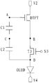
- FIG. 2 is a circuit diagram of a pixel circuit provided by an embodiment of the present disclosure
- FIG. 3 is a flowchart of steps of a pixel circuit driving method according to an embodiment of the present disclosure
- FIG. 4 is a timing diagram of timing signals in a pixel circuit according to an embodiment of the present disclosure.
- FIG. 5 is an equivalent circuit diagram of a pixel circuit in a first stage according to an embodiment of the present disclosure
- FIG. 6 is an equivalent circuit diagram of a pixel circuit in a second stage according to an embodiment of the present disclosure
- FIG. 7 is an equivalent circuit diagram of a pixel circuit in a third stage according to an embodiment of the present disclosure.
- the transistors used in all embodiments of the present disclosure may be thin film transistors or field effect transistors. Or use other devices with the same characteristics.
- the transistors employed in embodiments of the present disclosure may include a switching transistor and a driving transistor.
- the source and drain of the transistor used here are symmetrical, so the source and drain are interchangeable.
- one of the poles is referred to as a first end, and the other pole is referred to as a second end.
- the middle end of the transistor is the gate, the signal input is the source, and the signal output is the drain.
- the switching transistor may include a P-type switching transistor and an N-type switching transistor, wherein the P-type switching transistor is turned on when the gate is at a low level, and is turned off when the gate is at a high level, and the N-type The switching transistor is turned on when the gate is at a high level and turned off when the gate is at a low level.
- the driving transistor may include a P-type driving transistor and an N-type driving transistor, wherein the P-type driving transistor has a gate voltage at a low level (a gate voltage is less than a source voltage) and an absolute value of a gate-source voltage difference is greater than a threshold value When the voltage is in an amplified state or a saturated state, and the gate voltage of the N-type driving transistor is at a high level (the gate voltage is greater than the source voltage) and the absolute value of the gate-source voltage difference is greater than the threshold voltage, it is in an amplified state or Saturated state.
- a pixel circuit provided by an embodiment of the present disclosure includes a threshold compensation unit 11 , a driving unit 12 , a data writing unit 13 , a reset unit 14 , an electroluminescence unit 15 , and a feedback unit 16 .
- the threshold compensation unit 11 is connected to the first level terminal V1, the first scan signal terminal S1, the first node A, the second node B, and the third node C for being first under the control of the voltage of the first scan signal terminal S1.
- the voltage of the node A is aligned with the voltage of the first level terminal V1 and the voltage of the third node C is aligned with the voltage of the second node B.
- the threshold compensation unit 11 is further configured to cause the voltage of the first node A to change with the voltage of the third node C and store the voltage of the first node A and the voltage of the third node C.
- the driving unit 12 connects the first node A, the second node B, the second level terminal V2, the fourth node D, and the third scanning signal terminal S3 for the voltage at the first node A and the voltage of the third scanning signal terminal S3.
- the driving current is output through the fourth node D under the control, or the voltage of the second node B is adjusted to the voltage difference between the voltage of the first node A and the threshold voltage of the driving unit 12 under the control of the voltage of the first node A.
- the data writing unit 13 is connected to the data signal terminal DT, the second scanning signal terminal S2 and the third node C for controlling the voltage of the third node C and the data signal terminal DT under the control of the voltage of the second scanning signal terminal S2. The voltage is pulled.
- the reset unit 14 is connected to the second scan signal terminal S2, the third level terminal V3, and the fourth node D for controlling the voltage of the fourth node D and the third level terminal V3 under the control of the voltage of the second scan signal terminal S2. The voltage is pulled.
- the electroluminescent unit 15 is connected to the fourth node D and the fourth level terminal V4; the driving current for input through the fourth node D displays gray scale.
- the feedback unit 16 is connected to the third node C and the fourth node D for storing the voltage of the third node C and the voltage of the fourth node D and causing the voltage of the third node C to change with the voltage of the fourth node D.
- a pixel circuit provided by an embodiment of the present disclosure includes a threshold compensation unit, a driving unit, a data writing unit, a reset unit, an electroluminescence unit, and a feedback unit.
- the threshold compensation unit may align the voltage of the first node with the voltage of the first level terminal.
- the voltage of the first node may control the driving unit to adjust the voltage of the second node to a voltage difference between the voltage of the first node and the threshold voltage of the driving unit.
- the threshold compensation unit may also align the voltage of the third node with the voltage of the second node and store the voltage of the first node and the voltage of the third node.
- the data writing unit can pull the voltage of the third node and the voltage of the data signal terminal.
- the reset unit can pull the voltage of the fourth node and the voltage of the third level terminal.
- the threshold compensation unit may also cause the voltage of the first node to change with the voltage of the third node.
- the reset unit can pull the voltage of the fourth node and the voltage of the third level terminal.
- the feedback unit may cause the voltage of the third node to change with the voltage of the fourth node.
- the voltage of the first node is changed to a voltage sum obtained by adding the voltage difference between the threshold voltage of the driving unit and the voltage of the third level terminal from the data signal terminal voltage, so that the driving current output by the driving unit is made.
- the size is independent of the threshold of the drive unit, thereby eliminating the effect of the drive unit threshold voltage on the drive current. Thereby, the stability of the drive current can be improved, and the uniformity of the display brightness of the display device can be improved.
- the threshold compensation unit 11 may include a first transistor T1, a second transistor T2, and a first capacitor C1.
- the first end of the first transistor T1 is connected to the first level terminal V1
- the second end of the first transistor T1 is connected to the first node A
- the gate of the first transistor T1 is connected to the first scan signal terminal S1.
- the first end of the second transistor T2 is connected to the second node B
- the second end of the second transistor T2 is connected to the third node C
- the gate of the second transistor T2 is connected to the first scan signal terminal S1.
- the first pole of the first capacitor C1 is connected to the first node A
- the second pole of the first capacitor C1 is connected to the third node C.
- the driving unit 12 may include a driving transistor DTFT and a third transistor T3.
- the source of the driving transistor DTFT is connected to the second level terminal V2, and the driving transistor DTFT
- the drain is connected to the second node B, and the gate of the driving transistor DTFT is connected to the first node A.
- the first end of the third transistor T3 is connected to the second node B, the second end of the third transistor T3 is connected to the fourth node D, and the gate of the third transistor T3 is connected to the third scan signal terminal S3.
- the data writing unit 13 may include a fourth transistor T4.
- the first end of the fourth transistor T4 is connected to the data signal terminal DT, the second end of the fourth transistor T4 is connected to the third node C, and the gate of the fourth transistor T4 is connected to the second scan signal terminal S2.
- the reset unit 14 may include a fifth transistor T5.
- the first end of the fifth transistor T5 is connected to the third level terminal V3, the second end of the fifth transistor T5 is connected to the fourth node D, and the gate of the fifth transistor T5 is connected to the second scan signal terminal S2.
- the electroluminescent unit 15 may include a light emitting diode OLED.
- the anode of the light emitting diode OLED is connected to the fourth node D, and the cathode of the light emitting diode OLED is connected to the fourth level terminal V4.
- the feedback unit 16 may include a second capacitor C2.
- the first pole of the second capacitor C2 is connected to the third node C, and the second pole of the second capacitor C2 is connected to the fourth node D.
- FIG. 3 is a flowchart of steps of a pixel circuit driving method according to an embodiment of the present disclosure.
- the threshold compensation unit aligns the voltage of the first node with the voltage of the first level terminal and the voltage of the third node with the control of the voltage of the first scanning signal terminal.
- the voltage of the two nodes is pulled, and the driving unit adjusts the voltage of the second node to a voltage difference between the voltage of the first node and the threshold voltage of the driving unit under the control of the voltage of the first node, and the threshold compensation unit
- the voltage of the first node and the voltage of the third node are stored.
- the data writing unit pulls the voltage of the third node and the voltage of the data signal end under the control of the voltage of the second scanning signal end, and the threshold compensation unit makes the voltage of the first node and the voltage of the third node
- the reset unit pulls the voltage of the fourth node and the voltage of the third level terminal under the control of the voltage of the first scanning signal terminal
- the feedback unit causes the voltage of the third node to generate an equipotential with the voltage of the fourth node. Variety.
- the driving unit outputs a driving current through the fourth node under the control of the voltage of the first node and the voltage of the third scanning signal end, and the feedback unit causes the voltage of the third node to generate an equipotential with the voltage of the fourth node.
- the threshold compensation unit causes the voltage of the first node to change with the voltage of the third node, and the electroluminescent unit displays the gray level at the driving current input through the fourth node.
- the voltage of the first node is aligned with the voltage of the first level terminal, and the voltage of the second node is adjusted to the voltage of the first node.
- a voltage difference of a threshold voltage of the driving unit the voltage of the third node is aligned with the voltage of the second node, and the voltage of the first node and the voltage of the third node are stored;
- the voltage of the third node is Straightening with the voltage of the data signal terminal, aligning the voltage of the fourth node with the voltage of the third level terminal, and then causing the equipotential change of the voltage of the third node and the voltage of the fourth node, the voltage of the first node and the third
- the voltage of the node changes with an equal potential; during the third phase, under the control of the voltage of the first node, the driving current is output through the fourth node, and the gray scale is displayed by the electroluminescent unit.
- the voltage of the first node is changed to a voltage sum obtained by adding the threshold voltage of the driving unit to the voltage difference obtained by subtracting the voltage of the third level terminal from the voltage of the data signal terminal, so that the output of the driving unit is output.
- the drive current is not affected by the threshold voltage of the drive unit.
- the pixel circuit driving method provided by the embodiment of the present disclosure can improve the stability of the driving current, thereby improving the uniformity of the display brightness of the display device.
- the transistors in the pixel circuit may be N-type transistors, and the first level terminal V1 and the third level terminal V3 provide a reference voltage (the voltage value thereof may be according to a specific use scenario of the pixel circuit.
- the setting is not limited herein.
- the second level terminal V2 provides a high level
- the fourth level terminal V4 provides a low level (for example, the fourth level terminal V4 may be a ground terminal).
- the timing state of the first scanning signal terminal S1, the second scanning signal terminal S2, the third scanning signal terminal S3, and the data signal terminal DT in the pixel circuit in this case is as shown in FIG.
- V 1 is the voltage of the first level terminal
- V th is the threshold voltage of the driving transistor DTFT
- the first capacitor C1 stores the voltages of the first node A and the third node C.
- V 3 may be a reference voltage
- the voltage value of V 3 may be set according to a usage scenario of the pixel circuit.
- the illuminating voltage of the OLED in the previous frame is cleared by the voltage value of V 3 so that the reset unit in the above embodiment can avoid the influence of the illuminating voltage of the OLED in the previous frame on the brightness of the gray scale of the OLED display.
- the current flowing through the OLED is:
- ⁇ , C ox is the process constant
- W is the channel width of the driving transistor DTFT
- L is the channel length of the driving transistor DTFT
- W and L are selectively designtable constants.
- the drive current I oled is not affected by the threshold voltage V th of the drive transistor DTFT, but is only related to the voltages of the data signal terminal DT and the third level terminal V3. Therefore, the pixel driving circuit can output a stable driving current without being affected by the threshold voltage Vth of the driving transistor DTFT.
- first capacitor C1 and the second capacitor C2 in the above embodiment are connected in series, and the first pole of C1 is connected to the gate of the driving transistor DTFT, the second pole of C2 is connected to the drain of the driving transistor DTFT, and the gate of the driving transistor DTFT is Floating.
- Capacitors C1 and C2 do not have a charge and discharge path. Therefore, even if the voltage of the fourth level terminal V4 or the voltage of the light emitting diode OLED changes, the gate of the driving transistor undergoes an equipotential change, that is, the gate-source voltage difference of the driving transistor can be kept constant, thereby providing stable stability. Drive current.
- the first transistor, the second transistor, the third transistor, the fourth transistor, and the fifth transistor in the above embodiments may also be P-type transistors that are turned on when the gate is at a low level. If all transistors are P-type transistors, then only the timing state of each input signal needs to be re-adjusted. It is also possible to use both N-type transistors and P-type transistors. In this case, it is necessary to ensure that transistors of the same type are used by transistors with the same timing signal or voltage control. Considering the process technology of the transistor, the active layer doping materials of different types of transistors are different, so the use of a uniform type of transistor is more advantageous for the process of the pixel circuit.
- a further embodiment of the present disclosure provides a display device including the pixel circuit provided by any of the above embodiments.
- the display device may be any product or component having a display function such as an electronic paper, a mobile phone, a tablet computer, a television, a display, a notebook computer, a digital photo frame, a navigator, or the like.
- a pixel circuit of a display device includes a threshold compensation unit, a driving unit, a data writing unit, a reset unit, an electroluminescence unit, and a feedback unit.
- the threshold compensation unit may align the voltage of the first node with the voltage of the first level terminal.
- the voltage of the first node may control the driving unit to adjust the voltage of the second node to a voltage difference between the voltage of the first node and the threshold voltage of the driving unit.
- the threshold compensation unit may also align the voltage of the third node with the voltage of the second node and store the voltage of the first node and the voltage of the third node.
- the data writing unit can pull the voltage of the third node and the voltage of the data signal terminal.
- the reset unit can pull the voltage of the fourth node and the voltage of the third level terminal.
- the threshold compensation unit may also cause the voltage of the first node to change with the voltage of the third node.
- the reset unit can pull the voltage of the fourth node and the voltage of the third level terminal.
- the feedback unit may cause the voltage of the third node to change with the voltage of the fourth node.
- the voltage of the first node can be changed to a voltage sum obtained by adding a threshold voltage of the driving unit to a voltage difference obtained by subtracting a voltage of the third level terminal from the data signal terminal voltage, so that the driving current output by the driving unit is obtained.
- the size is independent of the threshold of the drive unit, thereby eliminating the effect of the drive unit threshold voltage on the drive current. Thereby, the stability of the drive current can be improved, and the uniformity of the display brightness of the display device can be improved.
Landscapes
- Engineering & Computer Science (AREA)
- Physics & Mathematics (AREA)
- Computer Hardware Design (AREA)
- General Physics & Mathematics (AREA)
- Theoretical Computer Science (AREA)
- Optics & Photonics (AREA)
- Control Of Indicators Other Than Cathode Ray Tubes (AREA)
- Control Of El Displays (AREA)
- Electroluminescent Light Sources (AREA)
Abstract
Description

Claims (9)
- 一种像素电路,包括:阈值补偿单元,其连接第一电平端、第一扫描信号端、第一节点、第二节点以及第三节点,用于在所述第一扫描信号端的电压的控制下将所述第一节点的电压与所述第一电平端的电压拉齐以及将所述第三节点的电压与所述第二节点的电压拉齐,还用于使所述第一节点的电压与所述第三节点的电压发生等电势变化以及存储所述第一节点的电压和所述第三节点的电压;驱动单元,其连接所述第一节点、所述第二节点、第二电平端、第四节点和第三扫描信号端,用于在所述第一节点的电压和所述第三扫描信号端的电压的控制下通过所述第四节点输出驱动电流,或者在所述第一节点的电压的控制下将所述第二节点的电压调节为所述第一节点的电压与所述驱动单元的阈值电压的电压差;数据写入单元,其连接数据信号端、第二扫描信号端和所述第三节点,用于在所述第二扫描信号端的电压的控制下将所述第三节点的电压与所述数据信号端的电压拉齐;复位单元,其连接所述第二扫描信号端、第三电平端以及第四节点,用于在所述第二扫描信号端的电压的控制下将所述第四节点的电压与所述第三电平端的电压拉齐;电致发光单元,其连接所述第四节点和第四电平端,用于通过所述第四节点输入的驱动电流显示灰阶;以及反馈单元,其连接所述第三节点和第四节点,用于存储所述第三节点的电压和所述第四节点的电压以及使所述第三节点的电压所述与第四节点的电压发生等电势变化。
- 根据权利要求1所述的像素电路,其中,所述阈值补偿单元包括:第一晶体管,其第一端连接所述第一电平端,其第二端连接所述第一节点,并且其栅极连接所述第一扫描信号端;第二晶体管,其第一端连接所述第二节点,其第二端连接所述第三节点,并且其栅极连接所述第一扫描信号端;以及第一电容,其第一极连接所述第一节点,并且其第二极连接所述第三节 点。
- 根据权利要求1所述的像素电路,其中,所述驱动单元包括:驱动晶体管,其源极连接所述第二电平端,其漏极连接所述第二节点,并且其栅极连接所述第一节点;第三晶体管,其第一端连接所述第二节点,其第二端连接所述第四节点,并且其栅极连接所述第三扫描信号端。
- 根据权利要求1所述的像素电路,其中,所述数据写入单元包括:第四晶体管,其第一端连接所述数据信号端,其第二端连接所述第三节点,并且其栅极连接所述第二扫描信号端。
- 根据权利要求1所述的像素电路,其中,所述复位单元包括:第五晶体管,其第一端连接所述第三电平端,其第二端连接所述第四节点,并且其栅极连接所述第二扫描信号端。
- 根据权利要求1所述的像素电路,其中,所述电致发光单元包括:发光二极管,其阳极连接所述第四节点,并且其阴极连接所述第四电平端。
- 根据权利要求1所述的像素电路,其中,所述反馈单元包括:第二电容,其第一极连接所述第三节点,并且其第二极连接所述第四节点。
- 一种驱动根据权利要求1-7中的任一项所述的像素电路的驱动方法,包括:第一阶段,其中,阈值补偿单元在第一扫描信号端的电压的控制下将第一节点的电压与第一电平端的电压拉齐以及将第三节点的电压与第二节点的电压拉齐,驱动单元在所述第一节点的电压的控制下将所述第二节点的电压调节为所述第一节点的电压与所述驱动单元的阈值电压的电压差,所述阈值补偿单元存储所述第一节点的电压和所述第三节点的电压;第二阶段,其中,数据写入单元在第二扫描信号端的电压的控制下将所述第三节点的电压与数据信号端的电压拉齐,所述阈值补偿单元使所述第一节点的电压与所述第三节点的电压发生等电势变化,复位单元在所述第一扫描信号端的电压的控制下将第四节点的电压与第三电平端的电压拉齐,反馈单元使所述第三节点的电压与所述第四节点的电压发生等电势变化;以及第三阶段,其中,所述驱动单元在所述第一节点的电压和第三扫描信号端的电压的控制下通过第四节点输出驱动电流,所述反馈单元使所述第三节点的电压所述与第四节点的电压发生等电势变化,所述阈值补偿单元使所述第一节点的电压与所述第三节点的电压发生等电势变化,电致发光单元在通过所述第四节点输入的驱动电流显示灰阶。
- 一种显示装置,包括根据权利要求1-7中的任一项所述的像素电路。
Priority Applications (1)
| Application Number | Priority Date | Filing Date | Title |
|---|---|---|---|
| US15/519,673 US10192486B2 (en) | 2016-01-04 | 2016-07-28 | Pixel circuit, a driving method for driving the pixel circuit, and a display device |
Applications Claiming Priority (2)
| Application Number | Priority Date | Filing Date | Title |
|---|---|---|---|
| CN201610004113.8 | 2016-01-04 | ||
| CN201610004113.8A CN105489163A (zh) | 2016-01-04 | 2016-01-04 | 一种像素电路及其驱动方法和显示装置 |
Publications (1)
| Publication Number | Publication Date |
|---|---|
| WO2017117985A1 true WO2017117985A1 (zh) | 2017-07-13 |
Family
ID=55676120
Family Applications (1)
| Application Number | Title | Priority Date | Filing Date |
|---|---|---|---|
| PCT/CN2016/092087 Ceased WO2017117985A1 (zh) | 2016-01-04 | 2016-07-28 | 像素电路及其驱动方法和显示装置 |
Country Status (3)
| Country | Link |
|---|---|
| US (1) | US10192486B2 (zh) |
| CN (1) | CN105489163A (zh) |
| WO (1) | WO2017117985A1 (zh) |
Families Citing this family (9)
| Publication number | Priority date | Publication date | Assignee | Title |
|---|---|---|---|---|
| CN105489163A (zh) | 2016-01-04 | 2016-04-13 | 京东方科技集团股份有限公司 | 一种像素电路及其驱动方法和显示装置 |
| CN107204173B (zh) * | 2017-06-08 | 2019-06-28 | 京东方科技集团股份有限公司 | 一种像素电路及其驱动方法、显示面板 |
| CN107068060B (zh) * | 2017-06-14 | 2019-09-24 | 深圳市华星光电半导体显示技术有限公司 | Amoled像素驱动电路及像素驱动方法 |
| CN107393475A (zh) | 2017-08-10 | 2017-11-24 | 京东方科技集团股份有限公司 | 像素驱动电路、像素驱动方法和显示装置 |
| CN108806591B (zh) * | 2018-04-26 | 2020-05-26 | 北京大学深圳研究生院 | 像素装置、像素装置的驱动方法以及显示设备 |
| CN115602119B (zh) * | 2021-07-08 | 2026-03-17 | 乐金显示有限公司 | 像素电路及包括其的显示面板 |
| US12542106B2 (en) | 2023-01-30 | 2026-02-03 | Chengdu Boe Optoelectronics Technology Co., Ltd. | Pixel circuit, pixel driving method and display device |
| CN116092430A (zh) * | 2023-03-20 | 2023-05-09 | 惠科股份有限公司 | 像素驱动电路、时序控制方法和显示面板 |
| KR20250037019A (ko) * | 2023-09-07 | 2025-03-17 | 삼성디스플레이 주식회사 | 화소 및 이를 포함하는 표시장치 |
Citations (6)
| Publication number | Priority date | Publication date | Assignee | Title |
|---|---|---|---|---|
| US8242981B2 (en) * | 2008-03-31 | 2012-08-14 | Samsung Mobile Display Co., Ltd. | Pixel and organic light emitting display using the same |
| CN103413520A (zh) * | 2013-07-30 | 2013-11-27 | 京东方科技集团股份有限公司 | 像素驱动电路、显示装置和像素驱动方法 |
| CN103514833A (zh) * | 2012-06-14 | 2014-01-15 | 乐金显示有限公司 | 有机发光二极管显示装置及其驱动方法 |
| CN104821150A (zh) * | 2015-04-24 | 2015-08-05 | 北京大学深圳研究生院 | 像素电路及其驱动方法和显示装置 |
| CN105489163A (zh) * | 2016-01-04 | 2016-04-13 | 京东方科技集团股份有限公司 | 一种像素电路及其驱动方法和显示装置 |
| CN205282056U (zh) * | 2016-01-04 | 2016-06-01 | 京东方科技集团股份有限公司 | 一种像素电路和显示装置 |
Family Cites Families (6)
| Publication number | Priority date | Publication date | Assignee | Title |
|---|---|---|---|---|
| KR101074811B1 (ko) * | 2010-01-05 | 2011-10-19 | 삼성모바일디스플레이주식회사 | 화소 회로, 유기전계발광 표시 장치 및 이의 구동 방법 |
| KR101693693B1 (ko) * | 2010-08-02 | 2017-01-09 | 삼성디스플레이 주식회사 | 화소 및 이를 이용한 유기전계발광 표시장치 |
| CN103778689B (zh) | 2012-10-17 | 2016-03-09 | 刘全 | 一种面向个人用户的出入口全局控制方法和系统 |
| KR102187835B1 (ko) * | 2013-10-17 | 2020-12-07 | 엘지디스플레이 주식회사 | 유기 발광 다이오드 표시장치 및 그 구동 방법 |
| TWI498873B (zh) | 2013-12-04 | 2015-09-01 | Au Optronics Corp | 有機發光二極體電路及其驅動方法 |
| CN104409051A (zh) * | 2014-12-24 | 2015-03-11 | 京东方科技集团股份有限公司 | 一种像素电路、有机电致发光显示面板及显示装置 |
-
2016
- 2016-01-04 CN CN201610004113.8A patent/CN105489163A/zh active Pending
- 2016-07-28 US US15/519,673 patent/US10192486B2/en active Active
- 2016-07-28 WO PCT/CN2016/092087 patent/WO2017117985A1/zh not_active Ceased
Patent Citations (6)
| Publication number | Priority date | Publication date | Assignee | Title |
|---|---|---|---|---|
| US8242981B2 (en) * | 2008-03-31 | 2012-08-14 | Samsung Mobile Display Co., Ltd. | Pixel and organic light emitting display using the same |
| CN103514833A (zh) * | 2012-06-14 | 2014-01-15 | 乐金显示有限公司 | 有机发光二极管显示装置及其驱动方法 |
| CN103413520A (zh) * | 2013-07-30 | 2013-11-27 | 京东方科技集团股份有限公司 | 像素驱动电路、显示装置和像素驱动方法 |
| CN104821150A (zh) * | 2015-04-24 | 2015-08-05 | 北京大学深圳研究生院 | 像素电路及其驱动方法和显示装置 |
| CN105489163A (zh) * | 2016-01-04 | 2016-04-13 | 京东方科技集团股份有限公司 | 一种像素电路及其驱动方法和显示装置 |
| CN205282056U (zh) * | 2016-01-04 | 2016-06-01 | 京东方科技集团股份有限公司 | 一种像素电路和显示装置 |
Also Published As
| Publication number | Publication date |
|---|---|
| CN105489163A (zh) | 2016-04-13 |
| US20180096653A1 (en) | 2018-04-05 |
| US10192486B2 (en) | 2019-01-29 |
Similar Documents
| Publication | Publication Date | Title |
|---|---|---|
| US11127348B2 (en) | Pixel circuit, driving method thereof and display device | |
| CN109887464B (zh) | 像素电路及其驱动方法、显示面板和显示设备 | |
| CN109545145B (zh) | 像素电路及其驱动方法、显示装置 | |
| US11361711B2 (en) | Pixel circuit and driving method thereof, display substrate, and display apparatus | |
| WO2017117985A1 (zh) | 像素电路及其驱动方法和显示装置 | |
| US10083658B2 (en) | Pixel circuits with a compensation module and drive methods thereof, and related devices | |
| CN102708819B (zh) | 一种像素驱动电路及其驱动方法、阵列基板和显示装置 | |
| CN104851392B (zh) | 一种像素驱动电路及方法、阵列基板和显示装置 | |
| CN108806599B (zh) | 用于补偿oled像素电路的方法 | |
| US9734763B2 (en) | Pixel circuit, driving method and display apparatus | |
| US10679552B2 (en) | Pixel circuit and drive method thereof, and display panel and display device | |
| WO2019137105A1 (zh) | 像素电路、驱动方法、电致发光显示面板及显示装置 | |
| CN103971640A (zh) | 一种像素驱动电路及其驱动方法和显示装置 | |
| CN107369412B (zh) | 一种像素电路及其驱动方法、显示装置 | |
| WO2017045357A1 (zh) | 像素电路及其驱动方法、显示基板及显示装置 | |
| CN116631339A (zh) | 像素电路及其驱动方法、显示基板和显示装置 | |
| US11244624B2 (en) | Pixel circuit and driving method therefor, display substrate and display device | |
| WO2017031909A1 (zh) | 像素电路及其驱动方法、阵列基板、显示面板及显示装置 | |
| WO2020192278A1 (zh) | 像素电路及其驱动方法、显示基板、显示装置 | |
| WO2015169015A1 (zh) | 像素驱动电路、驱动方法、阵列基板及显示装置 | |
| WO2016023311A1 (zh) | 像素驱动电路及其驱动方法和显示装置 | |
| CN104599638A (zh) | 一种像素电路及其驱动方法和显示装置 | |
| US10957257B2 (en) | Pixel circuit, driving method thereof and display panel | |
| WO2019037536A1 (zh) | 像素电路及其驱动方法、显示装置 | |
| CN105045438A (zh) | 一种触控显示电路及其驱动方法、显示装置 |
Legal Events
| Date | Code | Title | Description |
|---|---|---|---|
| WWE | Wipo information: entry into national phase |
Ref document number: 15519673 Country of ref document: US |
|
| 121 | Ep: the epo has been informed by wipo that ep was designated in this application |
Ref document number: 16883119 Country of ref document: EP Kind code of ref document: A1 |
|
| NENP | Non-entry into the national phase |
Ref country code: DE |
|
| 122 | Ep: pct application non-entry in european phase |
Ref document number: 16883119 Country of ref document: EP Kind code of ref document: A1 |
|
| 32PN | Ep: public notification in the ep bulletin as address of the adressee cannot be established |
Free format text: NOTING OF LOSS OF RIGHTS PURSUANT TO RULE 112(1) EPC (EPO FORM 1205 DATED 26/06/2019) |
|
| 122 | Ep: pct application non-entry in european phase |
Ref document number: 16883119 Country of ref document: EP Kind code of ref document: A1 |