WO2017104149A1 - 設計方法、設計プログラム及び設計装置 - Google Patents
設計方法、設計プログラム及び設計装置 Download PDFInfo
- Publication number
- WO2017104149A1 WO2017104149A1 PCT/JP2016/063340 JP2016063340W WO2017104149A1 WO 2017104149 A1 WO2017104149 A1 WO 2017104149A1 JP 2016063340 W JP2016063340 W JP 2016063340W WO 2017104149 A1 WO2017104149 A1 WO 2017104149A1
- Authority
- WO
- WIPO (PCT)
- Prior art keywords
- bypass
- stages
- stage
- register
- circuit
- Prior art date
- Legal status (The legal status is an assumption and is not a legal conclusion. Google has not performed a legal analysis and makes no representation as to the accuracy of the status listed.)
- Ceased
Links
Images











Classifications
-
- G—PHYSICS
- G06—COMPUTING OR CALCULATING; COUNTING
- G06F—ELECTRIC DIGITAL DATA PROCESSING
- G06F30/00—Computer-aided design [CAD]
- G06F30/30—Circuit design
- G06F30/32—Circuit design at the digital level
- G06F30/327—Logic synthesis; Behaviour synthesis, e.g. mapping logic, HDL to netlist, high-level language to RTL or netlist
-
- G—PHYSICS
- G06—COMPUTING OR CALCULATING; COUNTING
- G06F—ELECTRIC DIGITAL DATA PROCESSING
- G06F2111/00—Details relating to CAD techniques
- G06F2111/04—Constraint-based CAD
-
- G—PHYSICS
- G06—COMPUTING OR CALCULATING; COUNTING
- G06F—ELECTRIC DIGITAL DATA PROCESSING
- G06F2119/00—Details relating to the type or aim of the analysis or the optimisation
- G06F2119/12—Timing analysis or timing optimisation
Definitions
- the present invention relates to a design method, a design program, and a design apparatus.
- RTL Register Transfer Level
- HD Hardware Description Language
- RTL design is becoming unable to cope with the circuit scale of an integrated circuit that is increasing year by year, and higher-level designs with higher abstraction than RTL design are beginning to be used.
- the behavioral description of an integrated circuit is generated using C / C ++ language or SystemC, which implements a class library for hardware description, and high-level synthesis (Behavioral Synthesis) or functional synthesis ( This is also called Functional (Synthesis).)
- a tool converts a behavioral description such as C language into a functional description that is an RTL description.
- the logic synthesis tool converts the RTL function description into a logic description that is a gate description (or netlist), and the automatic wiring tool performs layout design based on the netlist.
- Generate mask data for SoC System On Chip
- an FPGA logic synthesis tool generates configuration data for an FPGA (Field Programmable Gate Array) from the RTL function description.
- a high-level synthesis tool that converts behavioral descriptions in C language into functional descriptions in HDL is used.
- This high-level synthesis tool generates a hardware description in HDL having various circuit configurations from source code described in a software language with a high degree of abstraction based on the constraints of high-level synthesis.
- the constraints of high-level synthesis include, for example, operating speed (clock frequency), latency (number of clocks from input to output), number of arithmetic circuits and memories, circuit scale, circuit area, and the like.
- JP 2014-6650 A Japanese Patent Laid-Open No. 10-63713
- HDL high-level design
- HDL has poor readability and is difficult to artificially change. Therefore, in order to change the circuit configuration, it is necessary to change high-level synthesis again and perform high-level synthesis.
- an object of the first aspect of the disclosure is to provide a design method, a design program, and a design apparatus for generating a hardware description of an integrated circuit whose specifications can be easily changed.
- a first aspect of the disclosure is a design method including a high-level synthesis process for generating a hardware description of a circuit from a source code in which an operation is described in a software language. Based on a predetermined high-level synthesis constraint, a hardware description and a high-level synthesis report information describing a circuit having a plurality of stages and an interstage register provided between the stages are generated from the source code, A pattern having a combination of interstage register stages to be bypassed among the stages of bypass candidate interstage registers based on bypass constraint information having a constraint condition regarding bypass of the interstage registers and the high-level synthesis report information A bypass stage selection pattern having a plurality of In this design method, bypass report information including combination information of registers to be bypassed according to a predetermined priority condition is combined based on the bypass stage selection pattern.
- FIG. 10 is a flowchart of the high-level synthesis program ST10 in the present embodiment. It is a figure which shows the example of the register between stages and the register between stages which can be bypassed. It is a figure which shows an example of the circuit produced
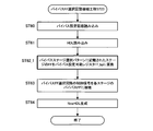
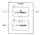
- FIG. 10 is a flowchart of a bypass setting circuit generation step ST22. It is a figure which shows the example of bypass stage information, a decoding table, and a bypass setting circuit. It is a flowchart figure of bypass setting circuit connection process ST23. It is a figure which shows the new circuit after connecting a bypass setting circuit. It is a figure explaining the outline of 2nd Embodiment.
- High level synthesis Also called High Level Synthesis (HLS), behavioral synthesis or functional synthesis.
- HLS High Level Synthesis
- HDL hardware description language
- RLT hardware description language
- High-level synthesis constraints are circuit constraints such as clock frequency, circuit area, circuit scale, power consumption, number of computing units, and are set in high-level synthesis.
- High-level synthesis library Also called technology library, it is a parameter corresponding to the circuit production line, and includes the speed of circuit elements such as gates, power consumption of circuit elements, area of circuit elements, and power supply voltage. Based on these parameters, the high-level synthesis tool estimates circuit timing, area, power consumption, and the like.
- High-level synthesis report A report generated by a high-level synthesis tool, which includes the delay time of each stage in the hardware description circuit and the number of registers between stages on the output side of each stage.
- Bypass restriction A restriction for converting an interstage register into a register that can be bypassed (interstage register as a candidate for bypass). For example, the number of stages of an interstage register that allows bypass setting (can be bypassed), bypass Any of the constraints such as a specific interstage register that allows setting, a specific interstage register that prohibits bypassing (cannot be bypassed), a minimum number of consecutive registers that prohibit bypassing, or any constraint combination.
- Bypass report A report in which bypass stage selection patterns are ranked according to priority conditions.
- Bypass stage A stage in which all interstage registers provided on the output side of the circuit stage are bypassed.
- bypass stage is also used to collectively refer to all interstage registers that are provided on the output side of the stage and are set to be bypassed.
- Circuit stage A combinational circuit sandwiched between registers on the input and output sides.
- Interstage registers Registers provided between circuit stages.
- ⁇ Bypass candidate interstage register Register that can be bypassed.
- Interstage register to be bypassed Bypass setting register.
- Bypass stage selection pattern A pattern having a combination of bypass setting register stages among the bypass setting register (bypass candidate registers) stages.
- Bypass stage information Information having all bypass stage selection patterns.
- Bypass setting circuit A circuit that bypass-sets registers that can be bypassed, and generates bypass control signals for bypass setting and bypass non-setting according to the mode setting value corresponding to the combination of registers to be bypassed. A circuit that outputs to a possible register.
- SRC Source code written in a high-level language, such as C language, C ++ language, or SystemC language.
- FF Flip-flop, a register between stages.
- EDA An abbreviation for Electric Design Automation, a general term for methods for automating semiconductor and other design work.
- CFG Abbreviation for Control Flow Graph, which represents the flow of circuit control.
- DFG Abbreviation for Data Flow Graph, which represents the circuit data flow.
- CDFG Abbreviation for Control Data Flow Graph, which is a combination of CFG and DFG, and is generated internally during high-level synthesis.
- FSSM Abbreviation of Finite State Machine, a finite state machine for control.
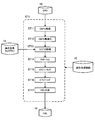
- FIG. 1 is a flowchart showing an integrated circuit design process including high-level synthesis.
- the function of the circuit is described in HDL based on the high-level synthesis constraint 12 and the high-level synthesis library 14 from the source code 10 describing the circuit operation in C language or the like based on the specifications of the integrated circuit. It has a high-level synthesis step ST1 that generates a hardware description 16.
- the high-level synthesis constraint 12 and the high-level synthesis library 14 are as described in the above definition collection.
- the design process includes a logic synthesis process ST2 for converting the HDL description 16 into a netlist 18 describing gates, and a layout process ST3 for laying out circuit elements and wirings connecting them based on the netlist.
- An integrated circuit such as a system-on-chip SoC is manufactured by a mask generation process ST4 for generating a mask from layout data generated by the layout process and a manufacturing process ST5 for forming an integrated circuit on a semiconductor substrate.
- the FPGA logic synthesis tool generates HDL description and FPGA configuration data. Then, the configuration data is downloaded to the FPGA, set in the field programmable gate array FPGA, and converted into an integrated circuit having a circuit configuration having a function of HDL description.
- FIG. 2 is a flowchart of the high-level synthesis process.
- the high-level synthesis step ST1 is specified as a CDFG creation step ST11 that interprets the source code and creates a control data flow diagram CDFG that shows data dependency and control dependency between operations, and its optimization step ST12
- the high-level synthesis process ST1 includes an allocation process ST14 that determines the type and number of arithmetic units, and a scheduling process ST15 that parallelizes operations in the CDFG based on the high-level synthesis constraint 12 and determines an execution cycle.
- Scheduling aims to minimize resource latency (number of clocks from input to output) with computational resources as a constraint, and conversely to minimize circuit resources with latency as constraints And time constraint scheduling.
- the high-level synthesis process ST1 has a binding process ST16 that maps the operator in the CDFG to an arithmetic unit, and maps variables and arrays to registers and memories. A circuit configuration having a register is determined.
- the HDL generation step ST17 generates an RTL description 16 that describes a circuit block that realizes the determined circuit configuration.
- High-level synthesis is a high-speed but large-scale circuit based on resource constraints such as the number of computing units and memory ports, and time constraints such as the number of execution cycles and the delay time of each stage, from source code describing a sequential operation algorithm. Also, it synthesizes various circuits, such as a low-speed but small-scale circuit that consumes less power.
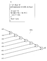
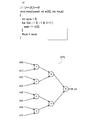
- FIGS. 3 and 4 are diagrams showing an example of the data flow graph DFG that is the source of the circuit when the source code is synthesized at a high level.
- the source code 10 in FIGS. 3 and 4 describes an operation of calculating and outputting the accumulated value sum of the eight pieces of data i [0] to i [7].
- the high-level synthesis tool generates the data flow graph DFG shown in FIG. 3 or 4 in the process of high-level synthesis of such source code 10.
- the data flow graph DFG in FIG. 3 sequentially performs addition operations in the same way as the source code addition order, whereas the data flow graph DFG in FIG. 4 changes the execution order of addition and adds four adders. Is used to complete the addition operation in three cycles.
- a circuit configuration in which one adder is operated repeatedly can be achieved, and the circuit scale (circuit area) can be reduced.
- the circuit scale is large, but the number of operation cycles (latency) can be reduced to three.
- Such a data flow graph is generated by the optimization process ST12.
- the circuit described in HDL generated by the high-level synthesis tool can have various configurations.
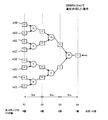
- FIG. 5 is a diagram illustrating an example of a circuit generated when the high-level synthesis constraint is set to a clock frequency of 200 MHz.
- the data flow graph on which the circuit of FIG. 5 is based is the data flow graph of FIG.
- a circuit having an interstage register FF between each adder as shown in FIG. 5 is generated.
- a flip-flop FF that is an interstage register is mapped between the input stage S1, the three addition stages S2, S3, S4, and the output stage.
- the delay time of the three addition stages is the same as 5 ns and the cycle of 5 MHz of the 200 MHz clock.
- the latency from input to output is 4 clocks (cycles), and the number of interstage registers FF on the output side of each of the input stage S1 and the three addition stages S2 to S4 is 8, 4, 2, One is a total of 15 pieces.
- the circuit of FIG. 5 can be operated at a maximum clock frequency of 200 MHz, and can also be operated at a clock frequency of 100 MHz when speed is not required.
- the number of FFs that are registers is always 7 and power saving is limited.
- FIG. 6 and 7 are diagrams showing examples of circuits generated when the high-level synthesis constraint is set to a clock frequency of 100 MHz.
- the flip-flop FF is mapped to the input stage S1, the first addition stage S2, and the third addition stage S4, and no flip-flop is mapped to the second addition stage.
- the latency from input to output is 3 clocks. Since no flip-flop is arranged on the output side of the two adders in the second stage, the number of FFs in each stage is eight, four, and one, for a total of 13.
- the flip-flop FF is mapped to the input stage S1, the second addition stage S3, and the third addition stage S4, and no flip-flop is mapped to the first addition stage.
- the delay time is 10 ns, which is the same as the clock cycle.
- the latency from input to output is 3 clocks.
- the number of FFs in each stage is eight, two, and one in total.
- the circuit of FIG. 5 can be operated at a high-speed clock frequency of 100 MHz, and the performance, which is the data processing amount per unit time, can be increased.
- the circuits of FIGS. 6 and 7 cannot operate at a high-speed clock frequency, the circuit scale is small, power consumption can be reduced, and the number of latency clocks (number of clock cycles) can be reduced.
- FIG. 8 is a diagram illustrating an example of a circuit generated when the high-level synthesis constraint is set to a clock frequency of 100 MHz.
- the design device 20 is a high-level synthesis dedicated computer in which high-level synthesis programs ST1 and ST20 are installed in a computer.
- the design device 20 includes a processor 21 such as a CPU, a memory 22, a high-level synthesis program ST1, ST20, storage (not shown) for storing various data, and a bus BUS connecting them.
- an input / output device such as a display and a keyboard and a network interface connected to a network are also provided.
- the high-level synthesis program ST10 of the present embodiment includes the high-level synthesis program ST1 described in FIG. 2 and a program ST20 for extending new functions according to the present embodiment.
- the new function expansion program ST20 includes a bypass stage extraction module ST21, a bypass setting circuit generation module ST22, and a bypass setting circuit connection module ST23. The function of these modules will be described in detail later.
- the data includes a high-level synthesis library 14 referred to by the high-level synthesis program ST20, a high-level synthesis constraint 12, a behavior description 10 in C language input by the high-level synthesis program ST20, and an HDL output by the high-level synthesis program ST20. And a circuit description 16. Furthermore, it has high level synthesis report information 30 generated by the high level synthesis program ST20.
- the data includes bypass constraint information 31 referred to by the new function expansion program ST20, a bypass report 32 generated by the new function expansion program ST20, bypass stage information 33, and an HDL description 34 of the bypass setting circuit.
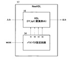
- the data includes a new circuit description 17 in which the HDL description 34 of the bypass setting circuit is combined with the circuit description 16 by HDL.
- This coalescing process is a process in which the bypass setting circuit connection module ST23 of the new function expansion program ST20 generates a circuit description 17 in which the bypass setting signal of the bypass setting circuit is connected to the bypass setting enable register in the circuit description 16.
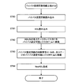
- FIG. 9 is a flowchart of the high-level synthesis program ST10 in the present embodiment.
- the high-level synthesis program ST10 in the present embodiment has a general high-level synthesis step ST1 and a new function expansion step ST20 added in the present embodiment.
- the outline of high-level synthesis in the present embodiment is as follows.
- the high-level synthesis program ST10 sets a high-level synthesis constraint and generates an HDL circuit description 16 that realizes the operation of the source code 10.
- the high-level synthesis is performed by setting the high-level synthesis constraint to the maximum clock frequency among the assumed operation states of the integrated circuit.
- the high-level synthesis program ST10 generates the HDL circuit description 16 in which the register FF is inserted at intervals corresponding to the period of the maximum clock frequency, for example, as shown in FIG.
- an interstage register FF is provided between the four stages of the input stage and the three addition stages.
- the newly added new function expansion program ST20 firstly generates a bypass stage information 33 and a bypass report 32 based on the high-level synthesis report information 30 and the bypass constraint information 31 (or a bypass stage extraction module (or Step) It has ST21.
- this bypass stage extraction step ST21 based on the bypass constraint condition of the bypass constraint information 31, the process of extracting which stage's output side register FF of the inter-stage register in the HDL circuit description 16 is to be a bypass setting register I do.
- all the combination patterns of registers to be bypassed are extracted based on the bypass constraint condition among the extracted registers that can be bypassed.
- bypass stage information 33 having preferably all combination patterns of register stages to be bypassed among a plurality of stages of registers that can be bypassed is generated.
- the bypass stage is a stage in which the interstage register on the output side of the circuit stage is bypassed as described in the definition of the terminology above, and all the interstage registers on the output side of the stage are bypassed.
- FIG. 10 is a diagram illustrating an example of an interstage register and an interstage register that can be bypassed.
- the interstage register FF is a general D-type flip-flop, which latches the input input to the data input terminal D at the timing of the rising edge (or falling edge) of the clock CLK and outputs the latched data from the output Q To do. Further, when an L level reset signal RST is input to the reset terminal RSTB, the latch data is reset to zero.
- the interstage register FF_bp that can be bypassed has a clock gate CG that supplies the clock CK to the clock terminal CLK according to the inversion logic of the bypass control signal S #.
- the clock gate CG prohibits the passage of the clock signal CK and stops the latch operation synchronized with the clock of the flip-flop FF.
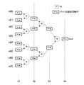
- FIG. 11 is a diagram showing an example of a circuit generated by high-level synthesis in the present embodiment.
- the circuit of FIG. 11 is a circuit in which the flip-flop FF, which is an interstage register of the circuit of FIG. 5, is replaced with an interstage register FF_bp that can be bypassed.
- the third stage inter-stage register FF_bp is deleted and becomes the same as the circuit of FIG. 6, and the latency from the input to the output is 3 clocks.
- the interstage register FF_bp that can be bypassed when the bypass is set, the clock gate CG prohibits the passage of the clock CK and stops the latch operation of the flip-flop.
- the circuit of FIG. 11 reduces the operation clock frequency to 100 MHz and reduces the power consumption of two interstage registers.
- bypass setting circuit that generates bypass control signals S1-S4 for bypass setting or bypass non-setting of the interstage register FF_bp that can be bypassed is provided, and the combination of bypass control signals output from the bypass setting circuit is externally set.
- the new function expansion program ST20 generates a bypass stage information 33 and a bypass report 32 based on the high-level synthesis report information 30 and the bypass constraint information 31 (or process). ) Has ST21.
- the high-level synthesis report information 30 is information generated by the high-level synthesis program ST1 in the high-level synthesis process, and includes timing information such as delay times of each stage, area information including the size of the area in which the circuit is formed, such as circuit scale, It includes information on the number of stages in the stage bypass setting register.
- the bypass constraint information 31 includes which stage's inter-stage register is a bypass setting enable register, which inter-stage register is bypass setting prohibition, and the like.
- the interstage registers FF of the circuit as shown in FIG. 5 generated in the high-level synthesis step ST1 can be bypassed among the interstage registers FF based on the bypass constraint information 31.
- the register to be replaced with the register FF_bp is extracted. Further, all of the combinations of stages of the interstage registers to be bypassed are extracted from the plurality of stages having the interstage register FF_bp that can be bypassed. Specific examples will be described later.
- the stage delay time, the number of interstage registers to be reduced, etc. are calculated for each combination pattern of stages having interstage registers to be bypassed.
- the bypass report 32 is generated.
- the bypass report 32 indicates how the bypass control signal S # should be set when priority is given to the clock frequency (that is, timing), and when the priority is given to the number of interstage registers to be reduced (that is, power consumption). It has information such as how to set S #.
- the user of the integrated circuit can refer to this bypass report, set the state of the register between stages that can be bypassed, and change the circuit to a desired operation. Specific examples will be described later.
- the new function expansion program ST20 includes a bypass setting circuit generation module (or process) ST22 that generates a description 34 of the bypass setting circuit based on the bypass stage information 33.
- the bypass setting circuit 34 sets a mode signal from the outside, thereby bypass-setting the combination of stages of the interstage registers to be bypass-set corresponding to the set mode signal.
- the new function expansion program ST20 has a bypass setting circuit connection module (or process) ST23 for generating a new HDL circuit 17.
- the bypass setting circuit connection step ST23 the interstage register in the circuit of the circuit description 16 in HDL generated by the high-level synthesis program ST1 is replaced with an interstage register that can be bypassed, and the bypassable interstage register and bypass setting A new HDL circuit description 17 is generated by connecting to the circuit 34. Specific examples will be described later.
- FIG. 12 is a diagram illustrating an example of bypass constraint information.
- FIG. 12 shows five bypass constraint conditions as an example.
- Item 1 is the number of bypass stages (or a range of numbers).
- the bypass stage means a stage in which a register on the output side of each stage among the four stages (input stage, three addition stages) in the circuit of FIG. 11 is set to be bypassed. Therefore, when the number of bypass stages is set to 1-2, one stage or two stages are simultaneously bypassed among the bypass-settable register groups on the output side of the four stages in FIG.
- the set value can be a minimum number, a maximum number, a fixed number, a range of numbers, and the like.
- Item 2 is the bypass prohibition of the first stage of input, and the set value is true or false.
- the register of the first stage S1 of the input in FIG. 11 is not replaced with the bypassable register FF_bp, and remains the normal register FF.
- the latch function of the register FF connected to the input terminal may be indispensable. In such a circuit, the set value is set to true.
- Item 3 is the bypass prohibition of the final stage of output, and the setting value is true or false.
- the register of the collective stage S4 in FIG. 11 is not replaced with the register FF_bp that can be set by bypass, and remains the normal register FF.
- the latch function of the register FF connected to the output terminal may be indispensable. In such a circuit, the set value is set to true.
- Item 4 is a specific stage in which bypass is prohibited, and the set value is a stage number. If Stage_5N (N is an integer) is set, the registers of multiples of 5 are prohibited from bypassing. Therefore, the register FF of the multiple of 5 stages is not replaced with the register FF_bp that can be set by bypass.
- Item 5 is a continuous stage that prohibits bypassing, and the setting value “0” is false, and is set not to prohibit bypass setting of the continuous stage (any number of continuous stages may be bypassed).
- the set value “2” means that the minimum number of consecutive stages that prohibits bypassing is two.
- bypass setting of two or more continuous stages that is, all the continuous stages is prohibited.
- the setting value “3” means that the same minimum value is 3, and bypass setting of two consecutive stages is permitted, but bypass setting of three or more consecutive stages is prohibited.
- a register FF of a stage other than the stage for which bypass setting is prohibited in items 2, 3, and 4 is specified as the bypass setting enable register FF_bp. Then, based on the constraint conditions of items 1 and 5, all the combination patterns of the stages for bypass setting the bypass setting enable register FF_bp are extracted.
- FIG. 13 is a diagram for explaining the outline of the bypass stage extraction process.
- FIG. 13 shows a circuit in which a 4-stage S1-S4 bypassable register FF_bp is provided between the input terminal SI and the output terminal SO similar to FIG.
- the high-level synthesis report information 30 includes the number of registers FF_bp of each stage S1-S4 and a delay time between the registers (delay time of each circuit stage). The numbers and delay times are as shown.
- bypass constraint information 31 has the number of bypass stages “1” of item 1
- the delay time when the stage S1 or S4 register is bypassed is as shown in the figure.
- the stage of the register to be bypassed (bypass stage) is extracted based on the bypass constraint information, and the bypass stage information including the bypass stage selection pattern and the bypass stage selection pattern is collected. Generate. Further, in the bypass stage extraction step, for each bypass stage selection pattern, a change in delay time due to bypass setting and the number of registers to be reduced are calculated, and a bypass report is created.
- FIG. 14 is a flowchart of the bypass stage extraction step ST21.
- FIG. 15 is a diagram illustrating an example of a detailed version of the bypass report. The bypass stage extraction process will be described with reference to a detailed version of the bypass report.
- the bypass report detail version includes a bypass stage selection pattern.
- the bypass stage extraction step ST21 reads bypass constraint information (ST31), reads high-level synthesis report information (ST32), and creates a bypass report (ST33). Then, the results generated in the bypass report creation process ST33 are aggregated to generate a detailed version and summary version of the bypass report (ST34), and further, the bypass stage selection patterns generated in the bypass report creation process ST33 are collected. Bypass stage information is generated (S35).
- bypass constraint is that there is no stage where bypassing is prohibited (setting values 2 and 3 are false, setting value 4 is none), and the minimum value of the continuous stage that prohibits bypassing of setting value 5 is “3” (continuous bypass stage) It is assumed that the number of bypass stages with the setting value 1 is 1-2 (1 to 2). As a result, as in the circuit shown in FIG. 11, the interstage register FF_bp that can be bypassed is inserted into all the stages S1 to S4.
- the bypass report creation step ST33 is repeated for each number of bypass stages, and ends when all the bypass stages are processed (ST40).
- the number of bypass stages is 1-2, so the number of bypass stages is 1 and 2.
- the number of bypass stages is selected (ST41).
- the bypass stage number 1 is selected from the bypass stage numbers 1 and 2 set by the bypass constraint.
- four patterns for bypass setting each of the four stages S1 to S4 in FIG. 11 are generated as bypass stage selection patterns (ST42). That is, a bypass stage selection pattern of “delay information report R1_1 when the number of bypass stages is one” in FIG. 15 is generated. The same applies to the report R2_1.
- This bypass stage selection pattern has four patterns in which each stage S1-S4 is set to bypass (bypass in the figure).
- this bypass stage selection pattern has six patterns in which two of the four stages S1 to S4 are set to bypass at the same time (bypass in the figure).
- the bypass stage selection pattern is a combination pattern of stages selected for bypass setting (bypass setting) among a plurality of stages that can be set to bypass.
- a bypass stage selection pattern is selected (ST44).
- the first bypass stage selection pattern pattern of mode setting M1S1 of the reports R1_1 and R2_1 in FIG. 15 is selected.
- the first bypass stage selection pattern is a pattern in which the output side register of the first stage S1 is set to bypass, and the remaining stages S2, S3, and S4 are not set to bypass.
- a mode setting name ID is assigned to the selected bypass stage selection pattern (ST45).
- the mode setting ID of the first pattern is “M1S1”.
- the delay time of each path (delay time between each register) is calculated, and the maximum path delay time is calculated from among them (ST46).
- the delay time is 6.65 ns, which is longer than the other path delay times, and the maximum path delay time is 6.6 ns.
- the number of registers for each stage is calculated (ST47).
- the number of registers FF in each stage is totaled, and the total number of registers and the number of registers reduced by bypass setting are calculated.
- the number of register FFs in stage S1 is 0, the total number of register FFs is 7, and the reduced number of register FFs is 8 in the leading pattern M1S1.
- the rank based on the timing priority (frequency priority) is higher in the pattern with the shorter maximum delay time.
- the mode setting M1S3 is ranked highest with the ranking TM1L1.
- mode setting M2S24 is ranked highest with ranking TM2L1.
- reports R1_2 and R2_2 are shown in FIG. 15 by calculating path delay time (ST46), calculating the number of registers and the number of registers reduced by bypass setting (ST47), and ranking (ST48, ST49). A report is created.
- bypass stage extraction step ST21 detailed and summary bypass reports are generated based on the calculation result of the bypass report creation step ST33 (ST34).
- the detailed version of the bypass report includes, for example, delay information reports R1_1 and R1_2 (bypass stage number 1) and register FF number information reports R2_1 and R2_2 (bypass stage number 2) for each bypass stage number. ).
- delay information reports R1_1 and R1_2 bypass stage number 1
- register FF number information reports R2_1 and R2_2 bypass stage number 2
- another priority condition for example, the uniformity of delay time, the balance order of the maximum delay time and the number of reduction registers (the order in which the total evaluation of both indicators is high, etc.), etc.
- FIG. 16 is a diagram illustrating an example of a summary version bypass report.
- report SR1 shows the highest ranking ID and its mode setting ID in timing priority (delay priority) and the highest ranking ID in power consumption priority (reduction FF number priority) for each number of bypass stages. And the mode setting ID. Since the report SR1 is a case where the bypass prohibition of the input first stage S1 is false (False), the highest level is the same as the detailed version bypass report of FIG.
- Report SR2 shows the highest ranking ID and its mode setting ID for each timing priority and power consumption priority for each number of bypass stages, similar to report SR1. However, since the bypass prohibition of the input first stage S1 is true, the highest level is shown when the bypass register selection pattern that bypasses the first stage S1 is excluded from the detailed version bypass report. .
- Report SR3 adds the maximum delay time for timing priority in report SR2.
- Report SR4 adds the reduction number of each register FF for power consumption priority in report SR2.
- the summary bypass report is a report that is referred to by the user when changing the circuit configuration after high-level synthesis, especially after manufacturing, and is a report edited from the detailed bypass report for such purposes. Preferably there is.
- the summary version bypass report shown in FIG. 16 is an example, and an edited report other than the above may be used. For example, a table of mode setting IDs and maximum delay times (or frequencies) sorted by timing priority according to the number of bypass stages, and a table of mode setting IDs and number of register FF reductions sorted by power consumption priority. Or, regardless of the number of bypass stages, a table of mode setting ID and maximum delay time (or frequency) simply sorted in order of timing priority, or a table of mode setting ID and number of registers reduced sorted by priority of power consumption , Etc.
- bypass stage information generation step ST35 In the bypass stage information generation step, all of the bypass stage selection patterns generated in the bypass report creation step ST33 and the mode setting IDs assigned thereto are collected. That is, the bypass stage information is a set of bypass stage selection patterns and mode setting IDs of the reports R1_1 and R1_2 or R2_1 and R2_2 in FIG. As a result, bypass stage information 33 shown in FIG. 18 is generated.
- FIG. 17 is a flowchart of the bypass setting circuit generation step ST22. As shown in FIG. 9, in the bypass setting circuit generation step, a description of the bypass setting circuit is generated from the bypass stage information 33 generated in the bypass stage extraction step ST21.
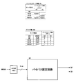
- FIG. 18 is a diagram illustrating examples of bypass stage information, a decoding table, and a bypass setting circuit.
- the flowchart of FIG. 17 will be described with reference to FIG.
- bypass stage information 33 is read (ST50).
- the bypass stage information is a table indicating which stage register (register on the output side of the stage) is bypass-set among the stages in correspondence with the mode setting ID. Therefore, the bypass stage selection pattern is regarded as a binary number, and a decode table 33D indicating the relationship among the mode setting ID, the mode code MODE, and the bypass stage selection pattern is generated (ST51).
- a description of the bypass setting circuit 34 that generates the bypass control signals S1-S4 as shown in the bypass stage selection pattern is generated (ST52).
- FIG. 19 is a flowchart of the bypass setting circuit connection step ST23.
- FIG. 20 is a diagram illustrating a new circuit after the bypass setting circuit is connected.
- the bypass setting circuit description 34 and the HDL circuit description 16 are read (ST60, ST61), and the bypass stage information 33 in the interstage register FF of each stage in the HDL circuit description 16 is read.
- the interstage register FF of the stage in which bypass setting is possible is replaced with the register FF_bp in which bypass setting is possible (ST62).
- the circuit description is changed so that the bypass control signals S1-S4 of the bypass setting circuit are connected to the bypass setting terminals of the bypass setting enable register FF_bp of each stage (SST63).
- a new HDL circuit description 17 in which the bypass setting circuit 34 is connected to the circuit of the HDL circuit description 16 is generated (ST64).
- bypass setting circuit 34 shown in FIG. 20 incorporates the mode register MODE_REG shown in FIG.
- FIG. 21 and 22 are diagrams for explaining the outline of the second embodiment.
- the example of FIG. 21 is an example in which all the interstage registers are replaced with the bypass setting register FF_bp, as in FIG.
- FIG. 22 shows a circuit configuration in the case where the bypass constraint information includes a constraint that prohibits bypass setting of the registers of the first stage and the last stage.
- the registers belonging to the first stage S1 and the registers belonging to the last stage S4 are prohibited from being bypassed, and thus remain normal registers FF.
- the other stage S2 and S3 registers are replaced with a bypass setting register FF_bp.
- FIG. 23 is a flowchart of the high-level synthesis program according to the second embodiment.
- the processing different from that of FIG. 9 of the first embodiment corresponds to a stage capable of bypass setting included in the bypass stage selection pattern in the bypass stage information by referring to the bypass stage information 33 in the bypass setting circuit connection step ST23. In this process, only the register to be replaced is replaced with the bypass setting register FF_bp. Other than that is the same as FIG.
- FIG. 24 is a flowchart of the bypass setting circuit connection step ST23 in the second embodiment.
- the processing different from FIG. 14 of the first embodiment is processing step ST42_1 for deleting the bypass prohibition stage from the bypass selection pattern, and the other processing is the same as FIG. That is, the pattern stage selection pattern generated in step ST42 is generated in the process where all the interstage registers are bypass candidates and are replaced with bypass configurable registers regardless of the bypass prohibition stage of the bypass constraint. .
- the bypass prohibition stage defined by the bypass constraint is deleted from the bypass candidates, and similarly, the bypass prohibition stage is deleted from the bypass stage selection pattern. For example, if the bypass constraint specifies the first stage S1 and the final stage S4 as bypass bypass stages, the stages S1 and S4 are bypassed from the bypass stage selection pattern in the detailed version bypass report of FIG. The existing pattern is deleted.
- FIG. 25 is a diagram illustrating an example of a detailed version bypass report according to the second embodiment.
- the pattern including the bypass prohibition stage is deleted from the bypass stage selection pattern in the detailed version bypass report of FIG.
- the shaded bypass stage selection pattern is deleted from the bypass report shown in FIG. 25, and the number of patterns is reduced to two, two if the number of bypass stages is one and one if the number of bypass stages is three.
- FIG. 26 is a diagram showing bypass stage information, a decoding table, and a bypass setting circuit.
- the bypass stage information 33 in FIG. 26 shows that the number of stages of the bypass stage selection pattern is reduced to two, S2 and S3, the mode setting ID is three circuit modes M0 in which all registers are not bypassed, The mode setting ID has been reduced to M1S2, M1S3, M2S23.
- the decoding table 33D is also reduced, so that the number of input bits of the bypass setting circuit 34 is two bits, and the number of bypass control signals S2 and S3 to be output is also reduced to two. Powered.
- FIG. 27 is a flowchart of the bypass setting circuit connection step ST23 in the second embodiment.
- the processing ST62 for replacing the register at each stage of the circuit in the circuit description in HDL of FIG. 19 with the register FF_bp that can be set by bypass is the register FF of the stage described in the bypass stage selection pattern in the bypass stage information 33 in FIG. Has been changed to processing ST62_1 in which is replaced with the bypass setting enable register FF_bp.
- the bypass stage selection pattern in the bypass stage information 33 does not include a stage that is already prohibited from bypassing due to the bypass constraint
- step ST62_1 the register FF of the stage prohibited from bypassing due to the bypass constraint is set to bypass. Not replaced with possible register FF_bp.
- FIG. 28 is a diagram showing a new HDL circuit to which the bypass setting circuit according to the second embodiment is connected.
- the bypass setting circuit 34 outputs only two bypass control signals S2 and S3, and the two bypass control signals are connected to the bypass setting enable register FF_bp in the circuit 16 based on HDL.
- one HDL circuit description is generated from one source code SRC.
- each circuit description is generated from a plurality of source codes, and an integrated circuit having circuits of these circuit descriptions is generated.
- FIG. 29 is a diagram showing a configuration of an integrated circuit of HDL description in the third embodiment.
- the integrated circuit LSI shown in FIG. 29 includes HDL description circuits 17_1 to 17_6 each having six HDL description circuits 16_1 to 16_6 connected to HDL description bypass setting circuits 34_1 to 34_6. Then, each bias setting circuit supplies a bypass control signal S # to the circuits 16_1 to 16_6 in accordance with the set value of the mode register MODE_REG, and performs bypass setting for the registers of a predetermined combination of stages.
Landscapes
- Engineering & Computer Science (AREA)
- Computer Hardware Design (AREA)
- Physics & Mathematics (AREA)
- Theoretical Computer Science (AREA)
- Evolutionary Computation (AREA)
- Geometry (AREA)
- General Engineering & Computer Science (AREA)
- General Physics & Mathematics (AREA)
- Design And Manufacture Of Integrated Circuits (AREA)
Abstract
スペックの変更が容易な集積回路のハードウエア記述を生成する設計方法、設計プログラム及び設計装置を提供する。ソフトウエア言語で動作が記述されたソースコードから回路のハードウエア記述を生成する高位合成処理を有する設計方法において、所定の高位合成制約に基づいて、ソースコードから、複数のステージと各ステージ間に設けられるステージ間レジスタとを有する回路を記述するハードウエア記述と高位合成レポート情報を生成し、ステージ間レジスタのバイパスに関する制約条件を有するバイパス制約情報と、高位合成レポート情報とに基づいて、バイパス候補のステージ間レジスタのステージのうちバイパス設定されるステージ間レジスタのステージの組合せを有するパターンを複数有するバイパスステージ選択パターンを決定し、バイパスステージ選択パターンに基づいて、所定の優先条件に応じた前記バイパス設定されるステージ間レジスタの組合せ情報を有するバイパスレポート情報を生成する、設計方法。
Description
本発明は,設計方法、設計プログラム及び設計装置に関する。
集積回路設計は、ハードウエア記述言語(HD: Hardware Description Language)を用いたRTL(Register Transfer Level)設計が主流である。RTL設計は、ゲートレベル設計に比べて設計抽象度が高いため、開発速度を速めることができる。
一方、RTL設計は、年々増加する集積回路の回路規模に対応できなくなりつつあり、RTL設計よりもさらに抽象度の高い高位設計が利用され始めている。高位設計では、C/C++言語や、ハードウエア記述向けクラスライブラリを実装したSystemCなどにより集積回路の動作記述を生成し、高位合成(High Level Synthesis)(または動作合成(Behavioral Synthesis)、機能合成(Functional Synthesis)とも呼ばれる。)ツールが、C言語等の動作記述をRTL記述である機能記述に変換する。そして、その後はRTL設計と同様に、論理合成ツールが、RTLの機能記述をゲート記述(またはネットリスト)である論理記述に変換し、さらに自動配線ツールがネットリストに基づいてレイアウト設計を行い、SoC(System On Chip)用のマスクデータを生成する。または、FPGA用の論理合成ツールが、RTLの機能記述からFPGA(Field Programmable Gate Array)用のコンフィグレーションデータを生成する。
このように、高位設計では、C言語などによる動作記述をHDLによる機能記述に変換する高位合成ツールが用いられる。この高位合成ツールは、高位合成の制約に基づいて、抽象度の高いソフトウエア言語で記述したソースコードから様々な回路構成を持ったHDLによるハードウエア記述を生成する。高位合成の制約は、例えば、動作速度(クロック周波数)、レイテンシ(入力から出力までのクロック数)、演算回路やメモリの数、回路規模や回路面積などが含まれる。
しかしながら、高位設計では、C言語等による動作記述からHDLによる機能記述に一旦変換した後は、HDLによる機能記述の回路を変更することは容易ではない。一般にHDLは可読性が乏しく人為的に変更することは困難である。そのため、回路構成を変更するためには、再度、高位合成の制約を変更して高位合成を行う必要がある。
また、一旦集積回路を製造し実装した後に、一時的に集積回路の速度(クロック周波数)やレイテンシ(入力してから出力されるまでのクロック数)を落として消費電力を下げたいというシーンや、逆に、速度を高くしてレイテンシを長くしてスループットを向上したいというシーンが存在する。しかし、製造された集積回路の回路構成を変更することは高いコストを要求される。そのため、クロック周波数を高くしてレイテンシを長くするハイスペックの高位合成制約で生成した回路を動作させる場合は、必要以上のスループットで動作し、また余分なエネルギーを消費することになる。逆に、クロック周波数を低くしてレイテンシを短くするロースペックの高位合成制約で生成した回路を動作させる場合は、低消費電力ではあるが、クロック周波数を高くしてレイテンシを短くすることはできない。
そこで,開示の第1の側面の目的は,スペックの変更が容易な集積回路のハードウエア記述を生成する設計方法、設計プログラム及び設計装置を提供することにある。
開示の第1の側面は,ソフトウエア言語で動作が記述されたソースコードから回路のハードウエア記述を生成する高位合成処理を有する設計方法において、
所定の高位合成制約に基づいて、前記ソースコードから、複数のステージと各ステージ間に設けられるステージ間レジスタとを有する回路を記述するハードウエア記述と高位合成レポート情報を生成し、
前記ステージ間レジスタのバイパスに関する制約条件を有するバイパス制約情報と、前記高位合成レポート情報とに基づいて、バイパス候補のステージ間レジスタのステージのうちバイパス設定されるステージ間レジスタのステージの組合せを有するパターンを複数有するバイパスステージ選択パターンを決定し、
前記バイパスステージ選択パターンに基づいて、所定の優先条件に応じた前記バイパス設定されるステージ間レジスタの組合せ情報を有するバイパスレポート情報を生成する、設計方法である。
所定の高位合成制約に基づいて、前記ソースコードから、複数のステージと各ステージ間に設けられるステージ間レジスタとを有する回路を記述するハードウエア記述と高位合成レポート情報を生成し、
前記ステージ間レジスタのバイパスに関する制約条件を有するバイパス制約情報と、前記高位合成レポート情報とに基づいて、バイパス候補のステージ間レジスタのステージのうちバイパス設定されるステージ間レジスタのステージの組合せを有するパターンを複数有するバイパスステージ選択パターンを決定し、
前記バイパスステージ選択パターンに基づいて、所定の優先条件に応じた前記バイパス設定されるステージ間レジスタの組合せ情報を有するバイパスレポート情報を生成する、設計方法である。
第1の側面によれば,集積回路のスペックの変更が容易になる。
[用語の定義]
以下は、本明細書で使用する用語の定義集である。
以下は、本明細書で使用する用語の定義集である。
高位合成:High Level Synthesis(HLS)、動作合成または機能合成とも呼ばれる。C言語などで回路の動作を記述したソースコードから、RLTなどのハードウエア記述言語(HDL)で回路の論理を記述したハードウエア記述を生成する処理。高位合成プログラム(または高位合成ツール)により処理される。
高位合成制約:クロック周波数、回路面積、回路規模、消費電力、演算器の数などの回路の制約であり、高位合成において設定される。
高位合成ライブラリ:テクノロジーライブラリとも呼ばれ、回路の製造ラインに対応したパラメータであり、ゲートなどの回路要素の速度、回路要素の消費電力、回路要素の面積、電源電圧などが含まれる。これらのパラメータに基づいて、高位合成ツールは、回路のタイミングや面積、消費電力などを見積る。
高位合成レポート:高位合成ツールが生成するレポートであり、ハードウエア記述の回路における各ステージの遅延時間、各ステージの出力側のステージ間レジスタの数を有する。
バイパス制約:ステージ間レジスタをバイパス設定可能なレジスタ(バイパス候補のステージ間レジスタ)に変換する場合の制約であり、例えば、バイパス設定を許可する(バイパス設定可能な)ステージ間レジスタのステージ数、バイパス設定を許可する特定のステージ間レジスタ、バイパスを禁止する(バイパス設定不可能な)特定のステージ間レジスタ、バイパスを禁止するステージ間レジスタの連続数の最小値などの制約のいずれか、または任意の組合せ。
バイパスレポート:バイパスステージ選択パターンを優先条件に従って順位付けしたレポート。
バイパスステージ:回路のステージの出力側に設けられた全てのステージ間レジスタがバイパスされたステージ。または、ステージの出力側に設けられバイパス設定された全てのステージ間レジスタを総称する場合にも「バイパスステージ」と称される。
回路のステージ:入力側と出力側のステージ間レジスタで挟まれた組み合わせ回路。
ステージ間レジスタ:回路のステージの間に設けられたレジスタ。
バイパス候補のステージ間レジスタ:バイパス設定可能レジスタ。
バイパス設定されるステージ間レジスタ:バイパス設定レジスタ。
バイパスステージ選択パターン:バイパス設定可能レジスタ(バイパス候補レジスタ)のステージのうちバイパス設定レジスタのステージの組合せを有するパターン。
バイパスステージ情報:バイパスステージ選択パターンを全て有する情報。
バイパス設定回路:バイパス設定可能レジスタをバイパス設定する回路であり、バイパス設定されるレジスタの組合せに対応するモード設定値に応じて、バイパス設定とバイパス非設定のバイパス制御信号を生成し、各バイパス設定可能レジスタに出力する回路。
SRC:高級言語で記述されたソースコードであり、C言語、C++言語、SystemC言語など。
FF:フリップフロップであり、ステージ間レジスタのこと。
EDA:Electric Design Automationの略であり、半導体などの設計作業を自動化する手法の総称。
CFG:Control Flow Graphの略であり、回路の制御の流れを表現した図。
DFG:Data Flow Graphの略であり、回路のデータの流れを表現した図。
CDFG:Control Data Flow Graphの略であり、CFGとDFGをあわせた図であり、高位合成時に内部で生成される。
FSM:Finite State Machineの略であり、制御用の有限状態機械。
[高位合成]
まず、高位合成について簡単に説明する。図1は、高位合成を含む集積回路の設計工程を示すフローチャート図である。集積回路の設計工程は、集積回路の仕様に基づいてC言語などで回路動作を記述したソースコード10から、高位合成制約12と高位合成ライブラリ14とに基づいて、HDLで回路の機能を記述したハードウエア記述16を生成する高位合成工程ST1を有する。高位合成制約12と高位合成ライブラリ14については、前述の定義集で説明したとおりである。
まず、高位合成について簡単に説明する。図1は、高位合成を含む集積回路の設計工程を示すフローチャート図である。集積回路の設計工程は、集積回路の仕様に基づいてC言語などで回路動作を記述したソースコード10から、高位合成制約12と高位合成ライブラリ14とに基づいて、HDLで回路の機能を記述したハードウエア記述16を生成する高位合成工程ST1を有する。高位合成制約12と高位合成ライブラリ14については、前述の定義集で説明したとおりである。
さらに、設計工程は、HDLの記述16をゲートを記述したネットリスト18に変換する論理合成工程ST2と、ネットリストに基づいて回路要素とそれを接続する配線をレイアウトするレイアウト工程ST3とを有する。レイアウト工程により生成されたレイアウトデータからマスクを生成するマスク生成工程ST4と半導体基板に集積回路を形成する製造工程ST5とにより、システム・オン・チップSoCなどの集積回路が製造される。
また、図示しないが、FPGA用の論理合成ツールが、HDL記述をFPGAのコンフィグレーションデータを生成する。そして、コンフィグレーションデータをFPGAにダウンロードしフィールドプログラマブルゲートアレイFPGAに設定し、HDL記述の機能を有する回路構成を有する集積回路に変換する。
図2は、高位合成工程のフローチャート図である。高位合成工程ST1は、ソースコードを解釈し、演算間のデータ依存関係や制御依存関係を示すコントロール・データ・フロー図CDFGを作成するCDFG作成工程ST11と、その最適化工程ST12と、指定されたテクノロジのライブラリを高位合成ライブラリ14から抽出するライブラリ処理工程ST13とを有する。
さらに、高位合成工程ST1は、演算器の種類や数などを決定するアロケーション工程ST14と、CDFG内の演算を高位合成制約12に基づいて並列化し、実行サイクルを決定するスケジューリング工程ST15とを有する。スケジューリングには、演算資源を制約にして回路のレイテンシ(入力から出力までのクロック数)の最小化を目的とする資源制約スケジューリングや、逆にレイテンシを制約にして回路の資源数の最小化を目的とする時間制約スケジューリングなどがある。
また、高位合成工程ST1は、CDFG内の演算子を演算器に、変数や配列をレジスタやメモリにマッピングするバインディング工程ST16を有し、このスケジューリング工程とバインディング工程により各ステージの組み合わせ回路とステージ間レジスタとを有する回路構成が決定される。そして、最後に、HDL生成工程ST17が、決定した回路構成を実現する回路ブロックを記述するRTL記述16を生成する。
RTL記述は、一般に可読性が低く人が修正をすることは困難である。したがって、高位合成されたRTL記述の回路において、クロック周波数や回路構成を変更するためには、高位合成制約を変更して再度高位合成を行い、ソースコードからRTL記述を生成する必要がある。さらに、RTL記述から製造された集積回路であるSoCのクロック周波数や回路構成を変更することは困難であり、高位合成から始まる回路設計工程を再度行うことが必要である。
高位合成は、逐次動作のアルゴリズムを記述したソースコードから、演算器やメモリポート数などの資源制約や、実行サイクル数や各ステージの遅延時間などの時間制約に基づいて、高速だが規模が大きい回路や、低速だが規模が小さく消費電力が少ない回路など様々な回路を合成する。
図3、図4は、ソースコードを高位合成した場合の回路の元となるデータフローグラフDFGの一例を示す図である。図3,図4のソースコード10は、8個のデータi[0]~i[7]の累積値sumを算出して出力する動作を記述する。
高位合成ツールは、このようなソースコード10を高位合成する過程で、図3または図4に示されるデータフローグラフDFGを生成する。図3のデータフローグラフDFGは、ソースコードの加算順と同じように加算演算を逐次実行するのに対して、図4のデータフローグラフDFGは、加算の実行順序を変更し4個の加算器を利用して加算演算を3サイクルで完了する。この場合、図3のデータフローグラフの場合は、1個の加算器を繰り返し動作させる回路構成にすることができ回路規模(回路面積)を小さくすることができるのに対して、図4のデータフローグラフの場合は、4個の加算器を有するので回路規模は大きいが演算サイクル数(レイテンシ)を3に少なくすることができる。このようなデータフローグラフは、最適化工程ST12により生成される。
図3,図4の例で分かるとおり、高位合成ツールにより生成されるHDL記述された回路は、様々な構成を有することが可能である。
図5は、高位合成制約をクロック周波数200MHzに設定した場合に生成される回路例を示す図である。図5の回路の元になるデータフローグラフは、図4のデータフローグラフである。図4のデータフローグラフにスケジューリングとバインディングを行うことで、図5のような各加算演算器の間にステージ間レジスタFFを有する回路を生成する。
図5の回路例は、入力ステージS1と3段の加算ステージS2, S3, S4と出力ステージそれぞれの間にステージ間レジスタであるフリップフロップFFがマッピングされている。そして、3段の加算ステージの遅延時間は5nsと200MHzのクロックの周期5nsと同じである。そして、入力から出力までのレイテンシは4クロック(サイクル)であり、入力ステージS1と3つの加算ステージS2~S4それぞれの出力側のステージ間レジスタFFの数は、8個、4個、2個、1個で合計15個である。
図5の回路は、最大クロック周波数200MHzで動作させることができるとともに、速度を要求しない時はクロック周波数100MHzで動作させることもできる。但し、レジスタであるFFの数は常時7個であり、省電力化は限定的である。
図6,図7は、高位合成制約をクロック周波数100MHzに設定した場合に生成される回路例を示す図である。図6の回路例は、入力ステージS1と初段の加算ステージS2と3段目の加算ステージS4にフリップフロップFFがマッピングされ、2段目の加算ステージにはフリップフロップはマッピングされていない。その結果、加算ステージは2段になっていて、それらの遅延時間は10nsとクロックの周期と同じである。そして、入力から出力までのレイテンシは3クロックである。また、2段目の2個の加算器の出力側にはフリップフロップが配置されていないので、各ステージのFFの数は、8個、4個、1個で合計13個である。
一方、図7の回路例は、入力ステージS1と2段目の加算ステージS3と3段目の加算ステージS4にフリップフロップFFがマッピングされ、初段の加算ステージにはフリップフロップはマッピングされていない。その結果、加算ステージは2段になっていて、それらの遅延時間は10nsとクロックの周期と同じである。そして、入力から出力までのレイテンシは3クロックである。また、初段の4個の加算器の出力側にはフリップフロップが配置されていないので、各ステージのFFの数は、8個、2個、1個で合計11個である。
図6,7の回路は、最大クロック周波数200MHzで動作させることはできないが、回路規模が小さくなり省電力化することができる。
このように、高位合成では、高位合成制約条件を変更することで、様々な構成の回路の記述を生成することができる。図5の回路は、高速のクロック周波数100MHzで動作させることができ、単位時間当たりのデータ処理量であるパフォーマンスを高くすることができる。一方、図6,7の回路は、高速クロック周波数での動作はできないが、回路規模が小さく、消費電力を低減することができ、さらに、レイテンシのクロック数(クロックサイクル数)を小さくできる。
しかしながら、高位合成によりHDL記述を生成した後では、図5の回路の記述を図6,7の回路の記述に変更すること、またはその逆方向の図6,7の回路の記述から図5の回路の記述に変更することは、前述のとおりHDL記述の可読性の低さなどから困難である。さらに、集積回路を製造した後では、両回路間の変更はほとんど不可能である。
[本実施の形態の高位合成]
図8は、高位合成制約をクロック周波数100MHzに設定した場合に生成される回路例を示す図である。設計装置20は、コンピュータに高位合成プログラムST1,ST20をインストールした高位合成専用コンピュータである。設計装置20は、CPUなどのプロセッサ21と、メモリ22と、高位合成プログラムST1,ST20と様々なデータを格納するストレージ(図示せず)と、それらを接続するバスBUSを有する。さらに、図示されていないが、ディスプレイやキーボードなどの入出力装置と、ネットワークに接続されるネットワークインターフェースなども有する。
図8は、高位合成制約をクロック周波数100MHzに設定した場合に生成される回路例を示す図である。設計装置20は、コンピュータに高位合成プログラムST1,ST20をインストールした高位合成専用コンピュータである。設計装置20は、CPUなどのプロセッサ21と、メモリ22と、高位合成プログラムST1,ST20と様々なデータを格納するストレージ(図示せず)と、それらを接続するバスBUSを有する。さらに、図示されていないが、ディスプレイやキーボードなどの入出力装置と、ネットワークに接続されるネットワークインターフェースなども有する。
本実施の形態の高位合成プログラムST10は、図2で説明した高位合成プログラムST1と、本実施の形態による新規機能を拡張するためのプログラムST20とを有する。この新規機能拡張プログラムST20は、バイパスステージ抽出モジュールST21と、バイパス設定回路生成モジュールST22と、バイパス設定回路接続モジュールST23とを有する。これらのモジュールの機能については後で詳述する。
データ類は、高位合成プログラムST20が参照する高位合成ライブラリ14と、高位合成制約12と、高位合成プログラムST20が入力するC言語などによるビヘイビア(動作)記述10と、高位合成プログラムST20が出力するHDLによる回路記述16とを有する。さらに、高位合成プログラムST20が生成する高位合成レポート情報30を有する。
さらに、データ類は、新規機能拡張プログラムST20が参照するバイパス制約情報31と、新規機能拡張プログラムST20が生成するバイパスレポート32と、バイパスステージ情報33と、バイパス設定回路のHDL記述34とを有する。また、データ類は、HDLによる回路記述16にバイパス設定回路のHDL記述34を合体した新しい回路記述17を有する。この合体処理は、新規機能拡張プログラムST20のバイパス設定回路接続モジュールST23が、回路記述16内のバイパス設定可能レジスタにバイパス設定回路のバイパス制御信号を接続した回路記述17を生成する処理である。
図9は、本実施の形態における高位合成プログラムST10のフローチャート図である。前述のとおり、本実施の形態における高位合成プログラムST10は、一般的な高位合成工程ST1と、本実施の形態で追加される新規機能拡張工程ST20とを有する。
本実施の形態における高位合成の概略は次のとおりである。
まず、高位合成プログラムST10は、高位合成制約を設定してソースコード10の動作を実現するHDLの回路記述16を生成する。本実施の形態では、高位合成制約を、想定される集積回路の動作状態のうち最大のクロック周波数に設定して、高位合成を行う。その結果、高位合成プログラムST10は、例えば図5に示したように、最大クロック周波数の周期に対応した間隔でレジスタFFが挿入されたHDLの回路記述16を生成する。図5の回路例では、入力ステージと3つの加算ステージの4つのステージの間にステージ間レジスタFFが設けられる。
そして、新たに追加した新規機能拡張プログラムST20は、第1に、高位合成レポート情報30とバイパス制約情報31とに基づいて、バイパスステージ情報33とバイパスレポート32とを生成するバイパスステージ抽出モジュール(または工程)ST21を有する。このバイパスステージ抽出工程ST21では、バイパス制約情報31のバイパス制約条件に基づいて、HDLの回路記述16内のステージ間レジスタのどのステージの出力側レジスタFFをバイパス設定可能なレジスタにするかの抽出処理を行う。さらに、抽出したバイパス設定可能なレジスタのうち、バイパス制約条件に基づいて、バイパス設定するレジスタの組合せパターンを好ましくは全て抽出する。この結果、バイパス設定可能なレジスタの複数のステージの中からバイパス設定するレジスタのステージの組合せパターンを、好ましくは、全て有するバイパスステージ情報33が生成される。
なお、バイパスステージとは、前述の用語の定義で説明したとおり、回路のステージの出力側のステージ間レジスタがバイパスされたステージであり、そのステージの出力側の全てのステージ間レジスタがバイパス設定される。
図10は、ステージ間レジスタとバイパス設定可能なステージ間レジスタの例を示す図である。ステージ間レジスタFFは、一般的なD型フリップフロップであり、データ入力端子Dに入力される入力をクロックCLKの立ち上がりエッジ(または立ち下がりエッジ)のタイミングでラッチし、出力Qからラッチデータを出力する。また、リセット端子RSTBにLレベルのリセット信号RSTが入力されるとラッチデータは0にリセットされる。
一方、バイパス設定可能なステージ間レジスタFF_bpは、D型フリップフロップFFに、入力端子Dに接続されたバイパスルートBPと、バイパスルートBPまたはフリップフロップFFのいずれかを選択するセレクタSELを有する。そして、バイパス制御信号S#がS#=1であれば、セレクタSELがバイパスルートBPを選択し、S#=0であれば、フリップフロップFFを選択する。これにより、バイパス設定可能なステージ間レジスタFF_bpは、バイパス制御信号S#を「1」に設定することでバイパス設定され、入力INは、クロックCKのタイミングに制約されずバイパスされる。
さらに、バイパス設定可能なステージ間レジスタFF_bpは、クロックCKをバイパス制御信号S#の反転論理に応じてクロック端子CLKに供給するクロックゲートCGを有する。このクロックゲートCGにより、バイパス制御信号S#がS#=1になると、クロックゲートCGはクロック信号CKの通過を禁止してフリップフロップFFのクロックに同期したラッチ動作を停止する。
したがって、ステージ間レジスタが、S#=1によりバイパス設定されると、クロックゲートCGはクロックCKの通過を禁止し、フリップフロップはラッチ動作を停止し、省電力状態になる。逆にS#=0によりバイパス設定が解除されると、クロックゲートはクロックCKの通過を許可し、フリップフロップはラッチ動作を行う。
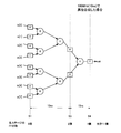
図11は、本実施の形態における高位合成で生成される回路の一例を示す図である。図11の回路は、図5の回路のステージ間レジスタであるフリップフロップFFを、バイパス設定可能なステージ間レジスタFF_bpに置き換えた回路である。そして、バイパス制御信号S1-S4をS1=0, S2=0, S3=1, S4=0に設定することで、4つのステージのステージ間レジスタのうち3段目のステージのステージ間レジスタFF_bpがバイパス設定されている。その結果、3段目のステージ間レジスタFF_bpが削除され、図6の回路と同じになり、入力から出力までは3クロックのレイテンシになる。
しかも、バイパス設定可能なステージ間レジスタFF_bpは、図10で説明したとおり、バイパス設定されるとクロックゲートCGがクロックCKの通過を禁止してフリップフロップのラッチ動作を停止する。その結果、図11の回路は、動作クロック周波数を100MHzに低速にするとともに、ステージ間レジスタ2個分の消費電力が削減される。
同様に、図11において、バイパス制御信号S1-S4をS1=0, S2=1, S3=0, S4=0に設定することで、4つのステージ間レジスタのうち2段目のステージ間レジスタFF_bpがバイパス設定され、さらに4個のステージ間レジスタの消費電力が削減され、実質的に図7の回路と同じになる。
後述するとおり、バイパス設定可能なステージ間レジスタFF_bpをバイパス設定またはバイパス非設定するバイパス制御信号S1-S4を生成するバイパス設定回路を設け、バイパス設定回路が出力するバイパス制御信号の組合せを、外部から設定するモード信号により変更可能にすることで、高位合成された回路の構成を変更することができる。製造済みの集積回路の段階でも同様に、モード信号により回路の構成を変更できる。
図9に戻り、第1に、新規機能拡張プログラムST20は、高位合成レポート情報30とバイパス制約情報31とに基づいて、バイパスステージ情報33とバイパスレポート32とを生成するバイパスステージ抽出モジュール(または工程)ST21を有する。
高位合成レポート情報30は、高位合成プログラムST1が高位合成過程で生成する情報であり、各ステージの遅延時間などのタイミング情報、回路規模など回路が形成されるエリアの大きさを有するエリア情報、各ステージのバイパス設定可能レジスタのステージ数の情報などを有する。バイパス制約情報31は、どのステージのステージ間レジスタをバイパス設定可能レジスタにするか、またどのステージ間レジスタをバイパス設定禁止にするか、などを有する。
したがって、バイパスステージ抽出工程ST21では、高位合成工程ST1により生成された図5のような回路のステージ間レジスタFFについて、バイパス制約情報31に基づいて、ステージ間レジスタFFのうちバイパス設定可能なステージ間レジスタFF_bpに置換するレジスタを抽出する。さらに、バイパス設定可能なステージ間レジスタFF_bpを持つ複数のステージうち、バイパス設定されるステージ間レジスタのステージの組合せのパターンを全て抽出する。具体例は後述する。
さらに、バイパスステージ抽出工程ST21では、高位合成レポート30に基づいて、バイパス設定されるステージ間レジスタを有するステージの組合せのパターンそれぞれについて、ステージの遅延時間や削減されるステージ間レジスタの数などを算出し、バイパスレポート32を生成する。バイパスレポート32は、クロック周波数(つまりタイミング)を優先した場合にバイパス制御信号S#をどのように設定すべきか、削減されるステージ間レジスタの数(つまり消費電力)を優先した場合にバイパス制御信号S#をどのように設定すべきかなどの情報を有する。
集積回路のユーザは、このバイパスレポートを参照して、バイパス設定可能なステージ間レジスタの状態を設定し、所望の動作の回路に変更可能である。具体例は後述する。
第2に、新規機能拡張プログラムST20は、バイパスステージ情報33に基づいて、バイパス設定回路の記述34を生成するバイパス設定回路生成モジュール(または工程)ST22を有する。バイパス設定回路34は、外部からモード信号を設定することで、設定したモード信号に対応するバイパス設定されるステージ間レジスタのステージの組合せをバイパス設定する。
第3に、新規機能拡張プログラムST20は、新たなHDLによる回路17を生成するバイパス設定回路接続モジュール(または工程)ST23を有する。バイパス設定回路接続工程ST23では、高位合成プログラムST1が生成したHDLによる回路記述16の回路内のステージ間レジスタをバイパス設定可能なステージ間レジスタに置換し、そのバイパス設定可能なステージ間レジスタとバイパス設定回路34とを接続して新たなHDLによる回路記述17を生成する。具体例は後述する。
以下、新規機能拡張プログラムST20について、具体例を交えて詳細に説明する。
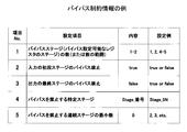
図12は、バイパス制約情報の一例を示す図である。図12には、一例として5項目のバイパス制約条件が示されている。項目1は、バイパスステージ数(または数の範囲)である。例えば、バイパスステージ数を1-2と設定すると、同時にバイパス設定されるレジスタのステージ数は、1ステージまたは2ステージに制約される。ここで、バイパスステージとは、図11の回路における4つのステージ(入力ステージ、3つの加算ステージ)のうち、各ステージの出力側のレジスタがバイパス設定されたステージを意味する。したがって、バイパスステージ数が1-2に設定されると、図11の4つのステージの出力側のバイパス設定可能レジスタ群のうち、同時に1ステージまたは2ステージがバイパス設定される。設定値は、最小数、最大数、固定数、数の範囲などが可能である。
項目2は、入力の初段ステージのバイパス禁止であり、設定値は真か偽かである。真に設定すると、入力の初段ステージのレジスタはバイパスが禁止され、したがって、図11の入力の初段ステージS1のレジスタは、バイパス設定可能なレジスタFF_bpに置換されず、通常のレジスタFFのままになる。一般的な回路の場合、入力端子に接続されるレジスタFFのラッチ機能が必須の場合があり、そのような回路の場合は設定値は真にされる。
項目3は、出力の最終ステージのバイパス禁止であり、設定値は真か偽である。真に設定すると、出力の最終ステージのレジスタはバイパスが禁止され、したがって、図11の集団ステージS4のレジスタは、バイパス設定可能なレジスタFF_bpに置換されず、通常のレジスタFFのままになる。一般的な回路の場合、出力端子に接続されるレジスタFFのラッチ機能が必須の場合があり、そのような回路の場合は設定値は真にされる。
項目4は、バイパスを禁止する特定のステージであり、設定値はステージ番号である。Stage_5N(Nは整数)と設定すると、5の倍数のステージのレジスタは、バイパスを禁止される。したがって、5の倍数のステージのレジスタFFは、バイパス設定可能なレジスタFF_bpに置換されない。
項目5は、バイパスを禁止する連続ステージであり、設定値「0」は偽であり、連続ステージのバイパス設定を禁止しない(いかなる数の連続ステージをバイパスしてよい)ことに設定される。設定値「2」は、バイパスを禁止する連続ステージの最小数が2であることを意味する。そして、2以上の連続ステージ、すなわち全ての連続ステージのバイパス設定は禁止される。設定値「3」は、同様の最小値が3であることを意味し、2つの連続ステージのバイパス設定は許可されるが、3つ以上の連続ステージのバイパス設定は禁止される。
図12のバイパス制約情報の例では、後述するバイパスステージ抽出工程ST21で、項目2,3,4でバイパス設定が禁止されているステージ以外のステージのレジスタFFが、バイパス設定可能レジスタFF_bpに特定される。そして、項目1,5の制約条件に基づいて、バイパス設定可能レジスタFF_bpをバイパス設定するステージの全組合せパターンが抽出される。
図13は、バイパスステージ抽出工程の概略を説明する図である。図13には、図11と同様の入力端子SIと出力端子SOとの間に4ステージS1-S4のバイパス設定可能なレジスタFF_bpが設けられた回路が示されている。高位合成レポート情報30は、図示されるとおり、各ステージS1-S4のレジスタFF_bpの数と、レジスタ間の遅延時間(各回路ステージの遅延時間)を有する。数と遅延時間は、図示されるとおりである。
ここで、バイパス制約情報31が、項目1のバイパスステージ数「1」を有する場合について説明する。ステージS2のバイパス設定可能レジスタFF_bpをバイパス設定してステージS2をバイパスステージにすると、ステージS2の4個のレジスタはバイパスされ、4個のレジスタが削除されその消費電力が削減される。さらに、データパスはS1からS3となり、その遅延時間は2.65ns+2.51ns=5.16nsとなる。
同様に、ステージS3のバイパス設定可能レジスタFF_bpをバイパス設定してステージS3をバイパスステージにすると、ステージS3の2個のレジスタはバイパスされ、2個のレジスタが削除されその消費電力が削減される。さらに、データパスはS2からS4となり、その遅延時間は2.51ns+2.23ns=4.74nsとなる。
また、ステージS1またはS4のレジスタをバイパス設定した場合の遅延時間は、図示されるとおりである。
図13に示すとおり、バイパスステージ抽出工程では、バイパス制約情報に基づいて、バイパス設定されるレジスタのステージ(バイパスステージ)を抽出し、バイパスステージ選択パターン及びバイパスステージ選択パターンを集めたバイパスステージ情報を生成する。さらに、バイパスステージ抽出工程では、バイパスステージ選択パターン毎に、バイパス設定されたことによる遅延時間の変化や削減されるレジスタ数を算出し、バイパスレポートを作成する。
[バイパスステージ抽出工程ST21]
図14は、バイパスステージ抽出工程ST21のフローチャート図である。また、図15は、バイパスレポートの詳細版の例を示す図である。バイパスステージ抽出工程について、バイパスレポートの詳細版を参照しながら説明する。なお、バイパスレポート詳細版にはバイパスステージ選択パターンが含まれている。
図14は、バイパスステージ抽出工程ST21のフローチャート図である。また、図15は、バイパスレポートの詳細版の例を示す図である。バイパスステージ抽出工程について、バイパスレポートの詳細版を参照しながら説明する。なお、バイパスレポート詳細版にはバイパスステージ選択パターンが含まれている。
バイパスステージ抽出工程ST21は、バイパス制約情報を読み込み(ST31)、高位合成レポート情報を読み込み(ST32)、バイパスレポートを作成する(ST33)。そして、バイパスレポート作成工程ST33で生成された結果を集計して、バイパスレポートの詳細版と要約版を生成し(ST34)、さらに、バイパスレポートの作成工程ST33で生成されたバイパスステージ選択パターンを集めてバイパスステージ情報を生成する(S35)。
次に、上記のバイパスレポートの作成工程ST33について説明する。ここで、バイパス制約は、バイパスが禁止されるステージなし(設定値2,3は偽、設定値4はなし)、設定値5のバイパスを禁止する連続ステージの最小値は「3」(連続バイパスステージ数は2まで許可)、設定値1のバイパスステージ数が1-2(1から2)の場合とする。その結果、図11に示す回路のように、全てのステージS1-S4にバイパス設定可能なステージ間レジスタFF_bpが挿入される。
バイパスレポートの作成工程ST33は、バイパスステージ数毎に繰り返され、全バイパスステージ数を処理すると終了する(ST40)。前述のバイパス制約は、バイパスステージ数が1-2であるので、バイパスステージ数は1と2である。
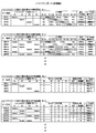
まず、バイパスレポートの作成工程は、バイパスステージ数を選択する(ST41)。例えば、バイパス制約で設定されたバイパスステージ数1,2のうちバイパスステージ数1を選択する。そして、バイパスレポートの作成工程は、図11の4つのステージS1-S4をそれぞれバイパス設定する4つのパターンがバイパスステージ選択パターンとして生成される(ST42)。すなわち、図15の「バイパスステージ数が1個の場合の遅延情報のレポートR1_1」のバイパスステージ選択パターンが生成される。レポートR2_1も同様である。このバイパスステージ選択パターンは、各ステージS1-S4がそれぞれバイパス設定(図中bypass)された4つのパターンを有する。
同様に、バイパスステージ数2を選択した場合は、図15の「バイパスステージ数が2個の場合の遅延情報のレポートR1_2」のバイパスステージ選択パターンが生成される。レポートR2_2も同様である。つまり、このバイパスステージ選択パターンは、4つのステージS1-S4のうち同時に2つのステージがバイパス設定(図中bypass)された6つのパターンを有する。
上記のとおり、バイパスステージ選択パターンは、バイパス設定可能な複数のステージのうちバイパス設定に選択された(バイパス設定された)ステージの組合せパターンである。
次に、バイパスレポートの作成工程は、生成した複数のバイパスステージ選択パターン毎に工程ST44-ST47を繰り返す(ST43)。まず、バイパスステージ選択パターンを選択する(ST44)。例えば、図15のレポートR1_1、R2_1の先頭のバイパスステージ選択パターン(モード設定M1S1のパターン)を選択するとする。先頭のバイパスステージ選択パターンは、最初のステージS1の出力側レジスタがバイパス設定され、残りのステージS2,S3,S4はバイパス設定されないパターンである。バイパスレポートの作成工程は、選択したバイパスステージ選択パターンにモード設定の名前(ID)を割り当てる(ST45)。レポートR1_1、R2_1の例では、先頭のパターンのモード設定のIDは、「M1S1」である。
そして、バイパス設定されたステージを考慮して、各パスの遅延時間(各レジスタ間の遅延時間)を算出し、その中から最大パス遅延時間を計算する(ST46)。レポートR1_1の例では、先頭のパターンM1S1はステージS1がバイパス設定されるので、それにより遅延時間が6.65nsと他のパス遅延時間より長くなり、最大パス遅延時間は6.6nsとなる。
さらに、各ステージのレジスタ数を計算する(ST47)。この計算では、各ステージのレジスタFFの数を集計して、レジスタ数の合計とバイパス設定により削減されたレジスタ数を算出する。レポートR2_1の例では、先頭のパターンM1S1はステージS1のレジスタFF数が0になり、レジスタFF数の合計が7,削減されたレジスタFF数が8になる。
レポートR1_1, R2_1の4つのバイパスステージ選択パターン全てについて、上記の工程ST44-ST47が完了すると(ST43のYES)、4つのパターンを最大パス遅延でランク付けし(ST48)、レジスタFF数またはレジスタFFの削減数でランク付けする(ST49)。ランク付けにしたがい、モード設定順位付けをレポートに追加する。その結果、図15のレポートR1_1, R2_1が生成される。
すなわち、最大遅延時間が短いパターンほどタイミング優先(周波数優先)に基づく順位が上位になる。例えば、レポートR1_1では、モード設定M1S3が順位付けTM1L1と最上位になっている。レポートR1_2では、モード設定M2S24が順位付けTM2L1と最上位である。
また、削減されるレジスタFF数が多いパターンほど消費電力優先に基づく順位が上位になる。例えば、レポートR2_1では、モード設定M1S1が順位付けPM1L1と最上位になっている。レポートR2_2では、モード設定M2S12が順位付けPM2L1と最上位になっている。
レポートR1_2,R2_2も同様にしてパス遅延時間の計算(ST46)とレジスタ数とバイパス設定されて削減されたレジスタ数の計算(ST47)とランク付け(ST48,ST49)により、図15に示されたレポートが作成される。
バイパスステージ抽出工程ST21では、上記のバイパスレポート作成工程ST33の計算結果に基づいて、詳細版と要約版のバイパスレポートを生成する(ST34)。詳細版のバイパスレポートは、図15に一例として示したように、例えば、バイパスステージ数別に遅延情報レポートR1_1,R1_2(バイパスステージ数1)と、レジスタFF数情報レポートR2_1,R2_2(バイパスステージ数2)とを有する。遅延情報、レジスタ数情報以外にユーザによる回路の変更の指標になるような別の優先条件がある場合は、その優先条件毎にレポートが生成されることが望ましい。別の優先条件としては、例えば遅延時間の均一性、最大遅延時間と削減レジスタ数のバランス順(両指標の合計評価が高い順など)などが考えられる。
図16は、要約版バイパスレポートの一例を示す図である。図16中、レポートSR1は、バイパスステージ数別に、タイミング優先(遅延時間優先)で最上位の順位付けIDとそのモード設定IDと、消費電力優先(削減FF数優先)で最上位の順位付けIDとそのモード設定IDをまとめたものである。レポートSR1は、入力の初段ステージS1のバイパス禁止が偽(False)の場合であるので、図15の詳細版バイパスレポートと最上位が同じになって
いる。
いる。
レポートSR2は、レポートSR1と同様に、バイパスステージ数別に、タイミング優先と消費電力優先それぞれで最上位の順位付けIDとそのモード設定IDを示す。但し、入力の初段ステージS1のバイパス禁止が真(True)の場合であるので、詳細版バイパスレポートから初段ステージS1をバイパスしているバイパスレジスタ選択パターンを除外した場合の最上位が示されている。
レポートSR3は、レポートSR2においてタイミング優先についてそれぞれの最大遅延時間を追加している。レポートSR4は、レポートSR2において消費電力優先についてそれぞれのレジスタFFの削減数を追加している。
要約版バイパスレポートは、高位合成の後において、特に製造された後において、ユーザが回路構成を変更するときに参照するレポートであり、そのような目的に応じて詳細版バイパスレポートを編集したレポートであることが好ましい。図16に示した要約版バイパスレポートは一例であり、上記以外の編集をしたレポートでもよい。たとえば、バイパスステージ数別のタイミング優先の順位でソートしたモード設定IDと最大遅延時間(または周波数)の表や、消費電力優先の順位でソートしたモード設定IDとレジスタFFの削減数の表。または、バイパスステージ数にかかわらず、単純にタイミング優先の順にソートしたモード設定IDと最大遅延時間(または周波数)の表や、消費電力優先の順位でソートしたモード設定IDとレジスタの削減数の表、などである。
次に、上記のバイパスステージ情報生成工程ST35について説明する。バイパスステージ情報生成工程では、バイパスレポート作成工程ST33で生成したバイパスステージ選択パターンとそれに割り当てたモード設定IDを全て集める。つまり、バイパスステージ情報は、図15のレポートR1_1,R1_2またはR2_1,R2_2のバイパスステージ選択パターンとモード設定IDの集合である。その結果、図18に示されるバイパスステージ情報33が生成される。
[バイパス設定回路生成工程ST22]
図17は、バイパス設定回路生成工程ST22のフローチャート図である。図9に示したとおり、バイパス設定回路生成工程は、バイパスステージ抽出工程ST21で生成したバイパスステージ情報33から、バイパス設定回路の記述を生成する。
図17は、バイパス設定回路生成工程ST22のフローチャート図である。図9に示したとおり、バイパス設定回路生成工程は、バイパスステージ抽出工程ST21で生成したバイパスステージ情報33から、バイパス設定回路の記述を生成する。
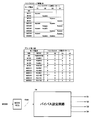
図18は、バイパスステージ情報とデコード表とバイパス設定回路の例を示す図である。図18を参照して、図17のフローチャート図を説明する。図17に示されるとおり、バイパス設定回路の生成工程は、まずバイパスステージ情報33を読み込む(ST50)。バイパスステージ情報は、モード設定IDに対応して各ステージのうちどのステージのレジスタ(ステージの出力側のレジスタ)をバイパス設定するかを示す表である。そこで、バイパスステージ選択パターンを2進数と見なして、モード設定IDとモードコードMODEとバイパスステージ選択パターンとの関係を示すデコード表33Dを生成する(ST51)。最後に、デコード表33Dに従ってモードコードMODEを設定するとバイパスステージ選択パターンに示されるようなバイパス制御信号S1-S4を生成するバイパス設定回路34の記述を生成する(ST52)。
[バイパス設定回路接続工程ST23]
図19は、バイパス設定回路接続工程ST23のフローチャート図である。図20は、バイパス設定回路を接続した後の新たな回路を示す図である。
図19は、バイパス設定回路接続工程ST23のフローチャート図である。図20は、バイパス設定回路を接続した後の新たな回路を示す図である。
バイパス設定回路の接続工程では、バイパス設定回路の記述34とHDLによる回路記述16をそれぞれ読み込み(ST60,ST61)、HDLの回路記述16内の各ステージのステージ間レジスタFFのうち、バイパスステージ情報33内のバイパス設定可能なステージのステージ間レジスタFFを、バイパス設定可能なレジスタFF_bpに置換する(ST62)。
さらに、接続工程では、バイパス設定回路のバイパス制御信号S1-S4を、各ステージのバイパス設定可能レジスタFF_bpのバイパス設定端子に接続するよう、回路記述を変更する(SST63)。その結果、HDLによる回路記述16の回路にバイパス設定回路34を接続した新たなHDLによる回路記述17が生成される(ST64)。
なお、図20に示したバイパス設定回路34は、図18のモードレジスタMODE_REGを内蔵する。
[第2の実施の形態]
第1の実施の形態では、高位合成工程ST1で生成したHDLによる回路内の全てのステージ間レジスタFFをバイパス設定可能レジスタFF_bpに置換した。第2の実施の形態では、バイパス制約情報にバイパスを禁止するステージの制約(項目2,3,4等)が含まれている場合に、バイパス設定が許可されるステージ間レジスタFFだけをバイパス設定可能レジスタFF_bpに置換する。これにより、バイアス設定回路を小さくできる。
第1の実施の形態では、高位合成工程ST1で生成したHDLによる回路内の全てのステージ間レジスタFFをバイパス設定可能レジスタFF_bpに置換した。第2の実施の形態では、バイパス制約情報にバイパスを禁止するステージの制約(項目2,3,4等)が含まれている場合に、バイパス設定が許可されるステージ間レジスタFFだけをバイパス設定可能レジスタFF_bpに置換する。これにより、バイアス設定回路を小さくできる。
図21、図22は、第2の実施の形態の概略を説明する図である。図21の例は、図11と同様に、全てのステージ間レジスタがバイパス設定可能レジスタFF_bpに置換された例である。それに対して、図22は、バイパス制約情報に初段ステージと最終段ステージのレジスタのバイパス設定を禁止する制約が含まれている場合の回路構成を示す。図22の例では、初段ステージS1に属するレジスタと最終段ステージS4に属するレジスタは、バイパス設定することは禁止されているので、通常のレジスタFFのままである。それ以外のステージS2,S3のレジスタがバイパス設定可能レジスタFF_bpに置換されている。
図22の回路の場合、バイパス設定の可能性があるステージS2,S3のみバイパス制御信号を供給すれば良いことになるので、バイパス設定回路の規模と、バイパス制御信号の数を小さくすることができ、回路面積、消費電力を抑制できる。
図23は、第2の実施の形態における高位合成プログラムのフローチャート図である。第1の実施の形態の図9と異なる処理は、バイパス設定回路接続工程ST23で、バイパスステージ情報33を参照して、バイパスステージ情報内のバイパスステージ選択パターンに含まれるバイパス設定可能なステージに対応するレジスタだけを、バイパス設定可能レジスタFF_bpに置換する処理である。それ以外は、図9と同じである。
図24は、第2の実施の形態におけるバイパス設定回路接続工程ST23のフローチャート図である。第1の実施の形態の図14と異なる処理は、バイパス禁止ステージをバイパス選択パターンから削除する処理工程ST42_1であり、それ以外は図14と同じである。すなわち、工程ST42で生成されたパターンステージ選択パターンは、バイパス制約のバイパス禁止ステージにかかわらず、全てのステージ間レジスタがバイパス候補でありバイパス設定可能レジスタに置換されるものと過程して生成される。しかし、第2の実施の形態では、工程ST42_1で、バイパス制約で規定されているバイパス禁止ステージをバイパス候補から削除し、同様にバイパス禁止ステージをバイパスステージ選択パターンから削除する。例えば、バイパス制約が初段ステージS1と最終段ステージS4とをバイパス禁止ステージに特定しているならば、図15の詳細版バイパスレポート内のバイパスステージ選択パターンから、ステージS1,S4をバイパス設定しているパターンが削除される。
図25は、第2の実施の形態における詳細版バイパスレポートの一例を示す図である。第2の実施の形態では、図15の詳細版バイパスレポート内のバイパスステージ選択パターンからバイパス禁止ステージを含むパターンを削除する。その結果、図25のバイパスレポートから、網掛けしたバイパスステージ選択パターンが削除され、パターン数がバイパスステージ数が1個の場合は2つ、2個の場合は1つ、合計3つに削減される。
図26は、バイパスステージ情報とデコード表とバイパス設定回路を示す図である。図18と比較すると、図26のバイパスステージ情報33は、バイパスステージ選択パターンのステージ数がS2,S3と2つに減り、モード設定IDが、全レジスタがバイパス設定されない回路モードM0と、3つのモード設定ID、M1S2, M1S3, M2S23に減っている。それに伴いデコード表33Dも小さくなり、よって、バイパス設定回路34の入力ビットは2ビットとなり、出力されるバイパス制御信号S2,S3も2本と少なくなり、その結果、バイパス設定回路の規模も小さく省電力化される。
図27は、第2の実施の形態におけるバイパス設定回路の接続工程ST23のフローチャート図である。図19のHDLによる回路記述の回路の各ステージのレジスタをバイパス設定可能なレジスタFF_bpに置換する処理ST62が、図27では、バイパスステージ情報33内のバイパスステージ選択パターンに記載されたステージのレジスタFFをバイパス設定可能レジスタFF_bpに置換する処理ST62_1に変更されている。つまり、バイパスステージ情報33内のバイパスステージ選択パターンは、既にバイパス制約でバイパスを禁止されているステージを含んでいないので、工程ST62_1では、バイパス制約でバイパスを禁止されたステージのレジスタFFはバイパス設定可能レジスタFF_bpに置換されない。
図28は、第2の実施の形態でのバイパス設定回路が接続された新たなHDLによる回路を示す図である。前述のとおり、バイパス設定回路34は、2つのバイパス制御信号S2,S3のみを出力し、2つのバイパス制御信号はHDLによる回路16内のバイパス設定可能レジスタFF_bpに接続される。
[第3の実施の形態]
第1、第2の実施の形態では、1つのソースコードSRCから1つのHDLによる回路記述を生成した。それに対して、第3の実施の形態では、複数のソースコードからそれぞれの回路記述を生成し、それらの回路記述の回路を有する集積回路を生成する。
第1、第2の実施の形態では、1つのソースコードSRCから1つのHDLによる回路記述を生成した。それに対して、第3の実施の形態では、複数のソースコードからそれぞれの回路記述を生成し、それらの回路記述の回路を有する集積回路を生成する。
図29は、第3の実施の形態におけるHDL記述の集積回路の構成を示す図である。図29の集積回路LSIは、6個のHDL記述の回路16_1~16_6それぞれに、HDL記述のバイパス設定回路34_1~34_6を接続したHDL記述の回路17_1~17_6を搭載する。そして、モードレジスタMODE_REGの設定値に対応して各バイアス設定回路がバイパス制御信号S#を回路16_1~16_6に供給して、所定の組合せのステージのレジスタにバイパス設定を行う。
以上のとおり、本実施の形態における高位合成を含む設計方法によれば、回路のステージ間レジスタをバイパス設定可能なレジスタに置換した回路のHDL記述と、バイパス制約にしたがう複数のバイパスステージ選択パターンからタイミング優先(ステージ内遅延時間優先)や消費電力優先(バイパス設定で削減されるレジスタ数優先)などの優先条件に応じたバイパスステージ選択パターンの順位などを有するバイパスレポート情報を生成する。したがって、ユーザは、HDL記述に基づいて生成した集積回路内の回路を、バイパスレポート情報に基づいて所望の動作モードに容易に変更することができる。
10:動作記述(C言語等で回路動作(ビヘイビア)を記述した記述)
ST10, ST1, ST20:高位合成プログラム
12:高位合成制約
14:高位合成ライブラリ
16:回路のハードウエア記述(HDLで回路の論理を記述した記述)
20:設計装置
31:バイパス制約
30:高位合成レポート
32:バイパスレポート
33:バイパスステージ情報(バイパスステージ選択パターンを全て有する情報)
34:バイパス設定回路(バイパス設定可能レジスタをバイパス設定する回路)
FF_bp:バイパス候補のステージ間レジスタ(バイパス設定可能レジスタ)
FF_bp:バイパス設定されるステージ間レジスタ(バイパス設定レジスタ)
S1-S4:バイパスステージ(出力側レジスタがバイパスされるステージ)
ST10, ST1, ST20:高位合成プログラム
12:高位合成制約
14:高位合成ライブラリ
16:回路のハードウエア記述(HDLで回路の論理を記述した記述)
20:設計装置
31:バイパス制約
30:高位合成レポート
32:バイパスレポート
33:バイパスステージ情報(バイパスステージ選択パターンを全て有する情報)
34:バイパス設定回路(バイパス設定可能レジスタをバイパス設定する回路)
FF_bp:バイパス候補のステージ間レジスタ(バイパス設定可能レジスタ)
FF_bp:バイパス設定されるステージ間レジスタ(バイパス設定レジスタ)
S1-S4:バイパスステージ(出力側レジスタがバイパスされるステージ)
Claims (13)
- ソフトウエア言語で動作が記述されたソースコードから回路のハードウエア記述を生成する高位合成処理を有する設計方法において、
所定の高位合成制約に基づいて、前記ソースコードから、複数のステージと各ステージ間に設けられるステージ間レジスタとを有する回路を記述するハードウエア記述と高位合成レポート情報を生成し、
前記ステージ間レジスタのバイパスに関する制約条件を有するバイパス制約情報と、前記高位合成レポート情報とに基づいて、バイパス候補のステージ間レジスタのステージのうちバイパス設定されるステージ間レジスタのステージの組合せを有するパターンを複数有するバイパスステージ選択パターンを決定し、
前記バイパスステージ選択パターンに基づいて、所定の優先条件に応じた前記バイパス設定されるステージ間レジスタの組合せ情報を有するバイパスレポート情報を生成する、設計方法。 - 前記ハードウエア記述を生成する工程において、前記高位合成制約は要求される最速のクロック周波数で動作可能な制約を有し、前記ハードウエア記述にしたがう回路の前記複数のステージの遅延時間が前記最速のクロック周波数の周期以下である、請求項1に記載の設計方法。
- 前記バイパス制約情報は、バイパス設定可能なステージ間レジスタのステージ数、バイパス設定可能な特定のステージ間レジスタのステージ、バイパス設定を禁止する特定のステージ間レジスタのステージ、バイパス設定を禁止するステージ間レジスタのステージの連続数の最小値のうちのいずれか、または任意の組合せを有する制約条件を有し、
前記バイパスステージ選択パターンは、前記バイパス制約情報に含まれる制約条件を満たすバイパス設定されるステージ間レジスタのステージの複数の組合せを有する、請求項2に記載の設計方法。 - 前記高位合成レポート情報は、前記複数のステージそれぞれの遅延時間と、各ステージが有するステージ間レジスタの数とを有し、
前記所定の優先条件は、前記複数の組合せのうち各組合せにおける最大ステージ遅延時間が短いことを優先する第1の優先条件と、前記複数の組合せの内各組合せにおけるバイパス設定されるステージ間レジスタの総数が多いことを優先する第2の優先条件のいずれかを有し、
前記バイパスレポート情報は、前記第1の優先条件の場合は前記最大ステージ遅延時間が短いまたは長い順位を有し、前記第2の優先条件の場合は前記バイパス設定されるステージ間レジスタの総数が多いまたは少ない順位を有する、請求項3に記載の設計方法。 - 前記バイパス候補のステージ間レジスタは、前記ステージの出力信号を保持するラッチ回路と、前記ラッチ回路をバイパスするバイパス配線と、前記ラッチ回路またはバイパス配線のいずれかをバイパス制御信号に基づいて選択するセレクタと、前記バイパス制御信号に基づいてクロックを通過または非通過するクロックゲートとを有し、
前記バイパス制御信号により前記バイパス候補のステージ間レジスタがバイパス設定される、請求項1に記載の設計方法。 - さらに、前記バイパスステージ選択パターン内の各パターンに対応するモード設定値に対応して、前記各パターン内の前記バイパス設定されるステージ間レジスタのステージの組合せに対応するバイパス設定またはバイパス非設定の前記バイパス制御信号を生成し、前記バイパス制御信号を前記バイパス候補のステージ間レジスタに供給するバイパス設定回路の記述を、前記ハードウエア記述に追加する工程を有する、請求項5に記載の設計方法。
- 前記バイパスステージ選択パターンを決定する工程は、
前記ハードウエア記述にしたがう回路に含まれる前記ステージ間レジスタから、前記制約条件で特定された前記バイパスを禁止する特定のステージのステージ間レジスタを除いて、前記バイパス候補のステージ間レジスタを選択する、請求項5に記載の設計方法。 - ソフトウエア言語で動作が記述されたソースコードから回路のハードウエア記述を生成する高位合成処理をコンピュータに実行させるコンピュータ読み取り可能な設計プログラムにおいて、前記高位合成処理は、
所定の高位合成制約に基づいて、前記ソースコードから、複数のステージと各ステージ間に設けられるステージ間レジスタとを有する回路を記述するハードウエア記述と高位合成レポート情報を生成することと、
前記ステージ間レジスタのバイパスに関する制約条件を有するバイパス制約情報と、前記高位合成レポート情報とに基づいて、バイパス候補のステージ間レジスタのステージのうちバイパス設定されるステージ間レジスタのステージの組合せを有するパターンを複数有するバイパスステージ選択パターンを決定することと、
前記バイパスステージ選択パターンに基づいて、所定の優先条件に応じた前記バイパス設定されるステージ間レジスタの組合せ情報を有するバイパスレポート情報を生成すること、とを有する設計プログラム。 - 前記ハードウエア記述を生成する工程において、前記高位合成制約は要求される最速のクロック周波数で動作可能な制約を有し、前記ハードウエア記述にしたがう回路の前記複数のステージの遅延時間が前記最速のクロック周波数の周期以下である、請求項8に記載の設計プログラム。
- 前記バイパス制約情報は、バイパス設定可能なステージ間レジスタのステージ数、バイパス設定可能な特定のステージ間レジスタのステージ、バイパス設定を禁止する特定のステージ間レジスタのステージ、バイパス設定を禁止するステージ間レジスタのステージの連続数の最小値のうちのいずれか、または任意の組合せを有する制約条件を有し、
前記バイパスステージ選択パターンは、前記バイパス制約情報に含まれる制約条件を満たすバイパス設定されるステージ間レジスタのステージの複数の組合せを有する、請求項9に記載の設計プログラム。 - ソフトウエア言語で動作が記述されたソースコードから回路のハードウエア記述を生成する高位合成処理部を有する設計装置において、
プロセッサと、
前記プロセッサにより実行される高位合成処理プログラムを記憶する記憶媒体とを有し、
前記高位合成処理プログラムは、
所定の高位合成制約に基づいて、前記ソースコードから、複数のステージと各ステージ間に設けられるステージ間レジスタとを有する回路を記述するハードウエア記述と高位合成レポート情報を生成することと、
前記ステージ間レジスタのバイパスに関する制約条件を有するバイパス制約情報と、前記高位合成レポート情報とに基づいて、バイパス候補のステージ間レジスタのステージのうちバイパス設定されるステージ間レジスタのステージの組合せを有するパターンを複数有するバイパスステージ選択パターンを決定することと、
前記バイパスステージ選択パターンに基づいて、所定の優先条件に応じた前記バイパス設定されるステージ間レジスタの組合せ情報を有するバイパスレポート情報を生成すること、とを有する設計装置。 - 前記ハードウエア記述を生成することにおいて、前記高位合成制約は要求される最速のクロック周波数で動作可能な制約を有し、前記ハードウエア記述にしたがう回路の前記複数のステージの遅延時間が前記最速のクロック周波数の周期以下である、請求項11に記載の設計装置。
- 前記バイパス制約情報は、バイパス設定可能なステージ間レジスタのステージ数、バイパス設定可能な特定のステージ間レジスタのステージ、バイパス設定を禁止する特定のステージ間レジスタのステージ、バイパス設定を禁止するステージ間レジスタのステージの連続数の最小値のうちのいずれか、または任意の組合せを有する制約条件を有し、
前記バイパスステージ選択パターンは、前記バイパス制約情報に含まれる制約条件を満たすバイパス設定されるステージ間レジスタのステージの複数の組合せを有する、請求項12に記載の設計装置。
Priority Applications (1)
| Application Number | Priority Date | Filing Date | Title |
|---|---|---|---|
| US15/968,327 US10606972B2 (en) | 2015-12-16 | 2018-05-01 | Method, design program, and design apparatus of a high level synthesis process of a circuit |
Applications Claiming Priority (2)
| Application Number | Priority Date | Filing Date | Title |
|---|---|---|---|
| JP2015-244798 | 2015-12-16 | ||
| JP2015244798A JP2017111591A (ja) | 2015-12-16 | 2015-12-16 | 設計方法、設計プログラム及び設計装置 |
Related Child Applications (1)
| Application Number | Title | Priority Date | Filing Date |
|---|---|---|---|
| US15/968,327 Continuation US10606972B2 (en) | 2015-12-16 | 2018-05-01 | Method, design program, and design apparatus of a high level synthesis process of a circuit |
Publications (1)
| Publication Number | Publication Date |
|---|---|
| WO2017104149A1 true WO2017104149A1 (ja) | 2017-06-22 |
Family
ID=59055959
Family Applications (1)
| Application Number | Title | Priority Date | Filing Date |
|---|---|---|---|
| PCT/JP2016/063340 Ceased WO2017104149A1 (ja) | 2015-12-16 | 2016-04-28 | 設計方法、設計プログラム及び設計装置 |
Country Status (3)
| Country | Link |
|---|---|
| US (1) | US10606972B2 (ja) |
| JP (1) | JP2017111591A (ja) |
| WO (1) | WO2017104149A1 (ja) |
Cited By (4)
| Publication number | Priority date | Publication date | Assignee | Title |
|---|---|---|---|---|
| US11888976B2 (en) | 2017-12-13 | 2024-01-30 | Nchain Licensing Ag | System and method for multi-party generation of blockchain-based smart contract |
| US12200103B2 (en) | 2017-11-09 | 2025-01-14 | Nchain Licensing Ag | System for simplifying executable instructions for optimised verifiable computation |
| US12273324B2 (en) | 2017-11-09 | 2025-04-08 | Nchain Licensing Ag | Systems and methods for ensuring correct execution of computer program using a mediator computer system |
| US12309257B2 (en) | 2017-12-15 | 2025-05-20 | Nchain Licensing Ag | System and method for authenticating off-chain data based on proof verification |
Families Citing this family (2)
| Publication number | Priority date | Publication date | Assignee | Title |
|---|---|---|---|---|
| JP6890741B2 (ja) | 2019-03-15 | 2021-06-18 | 三菱電機株式会社 | アーキテクチャ推定装置、アーキテクチャ推定方法、およびアーキテクチャ推定プログラム |
| KR102777276B1 (ko) | 2019-06-04 | 2025-03-10 | 삼성전자주식회사 | Fpga를 포함하는 전자 시스템 및 이의 동작 방법 |
Citations (2)
| Publication number | Priority date | Publication date | Assignee | Title |
|---|---|---|---|---|
| JP2000194739A (ja) * | 1998-12-28 | 2000-07-14 | Fuji Electric Co Ltd | モ―ド切換型論理回路の自動生成装置 |
| JP2014006650A (ja) * | 2012-06-22 | 2014-01-16 | Renesas Electronics Corp | 動作合成装置、動作合成方法、動作合成装置を備えたデータ処理システム、及び、動作合成プログラム |
Family Cites Families (3)
| Publication number | Priority date | Publication date | Assignee | Title |
|---|---|---|---|---|
| JP2972646B2 (ja) | 1996-06-14 | 1999-11-08 | 松下電器産業株式会社 | 機能設計方法、機能設計装置、及び機能設計プログラムが記録されたコンピュータ読み取り可能な記録媒体 |
| JP6255880B2 (ja) * | 2013-10-10 | 2018-01-10 | 株式会社ソシオネクスト | 高位合成用データ生成装置、高位合成装置、高位合成用データ生成方法及びプログラム |
| US9250900B1 (en) * | 2014-10-01 | 2016-02-02 | Cadence Design Systems, Inc. | Method, system, and computer program product for implementing a microprocessor with a customizable register file bypass network |
-
2015
- 2015-12-16 JP JP2015244798A patent/JP2017111591A/ja active Pending
-
2016
- 2016-04-28 WO PCT/JP2016/063340 patent/WO2017104149A1/ja not_active Ceased
-
2018
- 2018-05-01 US US15/968,327 patent/US10606972B2/en active Active
Patent Citations (2)
| Publication number | Priority date | Publication date | Assignee | Title |
|---|---|---|---|---|
| JP2000194739A (ja) * | 1998-12-28 | 2000-07-14 | Fuji Electric Co Ltd | モ―ド切換型論理回路の自動生成装置 |
| JP2014006650A (ja) * | 2012-06-22 | 2014-01-16 | Renesas Electronics Corp | 動作合成装置、動作合成方法、動作合成装置を備えたデータ処理システム、及び、動作合成プログラム |
Cited By (11)
| Publication number | Priority date | Publication date | Assignee | Title |
|---|---|---|---|---|
| US12200103B2 (en) | 2017-11-09 | 2025-01-14 | Nchain Licensing Ag | System for simplifying executable instructions for optimised verifiable computation |
| US12219044B2 (en) | 2017-11-09 | 2025-02-04 | Nchain Licensing Ag | System for securing verification key from alteration and verifying validity of a proof of correctness |
| US12273324B2 (en) | 2017-11-09 | 2025-04-08 | Nchain Licensing Ag | Systems and methods for ensuring correct execution of computer program using a mediator computer system |
| US12309168B2 (en) | 2017-11-09 | 2025-05-20 | Nchain Licensing Ag | Arithmetic enhancement of C-like smart contracts for verifiable computation |
| US12407693B2 (en) | 2017-11-09 | 2025-09-02 | Nchain Licensing Ag | System for securing verification key from alteration and verifying validity of a proof of correctness |
| US11888976B2 (en) | 2017-12-13 | 2024-01-30 | Nchain Licensing Ag | System and method for multi-party generation of blockchain-based smart contract |
| US12238206B2 (en) | 2017-12-13 | 2025-02-25 | Nchain Licensing Ag | System and method for securely sharing cryptographic material |
| US12294644B2 (en) | 2017-12-13 | 2025-05-06 | Nchain Licensing Ag | System and method for multi-party generation of blockchain-based smart contract |
| US12556378B2 (en) | 2017-12-13 | 2026-02-17 | Nchain Licensing Ag | System and method for securely sharing cryptographic material |
| US12574221B2 (en) | 2017-12-13 | 2026-03-10 | Nchain Licensing Ag | System and method for securely sharing cryptographic material |
| US12309257B2 (en) | 2017-12-15 | 2025-05-20 | Nchain Licensing Ag | System and method for authenticating off-chain data based on proof verification |
Also Published As
| Publication number | Publication date |
|---|---|
| JP2017111591A (ja) | 2017-06-22 |
| US20180246997A1 (en) | 2018-08-30 |
| US10606972B2 (en) | 2020-03-31 |
Similar Documents
| Publication | Publication Date | Title |
|---|---|---|
| JP3331968B2 (ja) | グリッチ分析と低減に重点をおいたレジスタトランスファレベルの電力消費最適化回路、方法、及び記録媒体 | |
| US10606972B2 (en) | Method, design program, and design apparatus of a high level synthesis process of a circuit | |
| CN104573169B (zh) | 以自动流水线操作能力设计集成电路的方法和工具 | |
| US8875071B2 (en) | Deployment of custom shift array macro cells in automated application specific integrated circuit design flow | |
| US9201996B2 (en) | Behavioral synthesis apparatus, behavioral synthesis method, data processing system including behavioral synthesis apparatus, and non-transitory computer readable medium storing behavioral synthesis program | |
| JP2000057201A (ja) | 低電力vlsiデザインのための制限付きレジスタ共用方法及びそのシステム | |
| US9727681B2 (en) | Generating specific memory models using generic memory models for designing memories in VLSI design | |
| US6845489B1 (en) | Database for design of integrated circuit device and method for designing integrated circuit device | |
| US9842187B1 (en) | Representation of complex timing characteristics of startpoint-endpoint pairs in a circuit design | |
| US20100253409A1 (en) | Clock generation system and clock dividing module | |
| US20050039152A1 (en) | Timing path detailer | |
| JP2004303022A (ja) | プリプロセッサ、集積回路の設計システム及び集積回路の設計方法 | |
| JP2008299464A (ja) | 消費電力計算方法、消費電力計算プログラムおよび消費電力計算装置 | |
| Chiou et al. | Synthesis of application-specific highly efficient multi-mode cores for embedded systems | |
| Chen et al. | An Open-Source $4\times 8$ Coarse-Grained Reconfigurable Array Using SkyWater 130 nm Technology and Agile Hardware Design Flow | |
| JP2010257003A (ja) | 論理等価性検証システム、論理等価性検証方法、半導体集積回路の製造方法、制御プログラムおよび可読記憶媒体 | |
| Loh et al. | Analysis of Logic synthesis results with various technology nodes for RISC-V design | |
| US20060190848A1 (en) | Low power consumption designing method of semiconductor integrated circuit | |
| JP6242170B2 (ja) | 回路設計支援装置及びプログラム | |
| Mehta et al. | A low-energy reconfigurable fabric for the supercisc architecture | |
| Lin et al. | A platform of resynthesizing a clock architecture into power-and-area effective clock trees | |
| JP3004589B2 (ja) | パストランジスタ論理設計方法 | |
| Masoumi et al. | New tool for converting high-level representations of finite state machines to verilog hdl | |
| Jozwiak et al. | Hardware synthesis for reconfigurable heterogeneous pipelined accelerators | |
| Lavagno et al. | Incremental high-level synthesis |
Legal Events
| Date | Code | Title | Description |
|---|---|---|---|
| 121 | Ep: the epo has been informed by wipo that ep was designated in this application |
Ref document number: 16875137 Country of ref document: EP Kind code of ref document: A1 |
|
| NENP | Non-entry into the national phase |
Ref country code: DE |
|
| 122 | Ep: pct application non-entry in european phase |
Ref document number: 16875137 Country of ref document: EP Kind code of ref document: A1 |