WO2017098537A1 - 磁気抵抗効果素子の製造方法および装置 - Google Patents
磁気抵抗効果素子の製造方法および装置 Download PDFInfo
- Publication number
- WO2017098537A1 WO2017098537A1 PCT/JP2015/006056 JP2015006056W WO2017098537A1 WO 2017098537 A1 WO2017098537 A1 WO 2017098537A1 JP 2015006056 W JP2015006056 W JP 2015006056W WO 2017098537 A1 WO2017098537 A1 WO 2017098537A1
- Authority
- WO
- WIPO (PCT)
- Prior art keywords
- substrate
- film
- cathode
- target
- center
- Prior art date
- Legal status (The legal status is an assumption and is not a legal conclusion. Google has not performed a legal analysis and makes no representation as to the accuracy of the status listed.)
- Ceased
Links
Images





Classifications
-
- C—CHEMISTRY; METALLURGY
- C23—COATING METALLIC MATERIAL; COATING MATERIAL WITH METALLIC MATERIAL; CHEMICAL SURFACE TREATMENT; DIFFUSION TREATMENT OF METALLIC MATERIAL; COATING BY VACUUM EVAPORATION, BY SPUTTERING, BY ION IMPLANTATION OR BY CHEMICAL VAPOUR DEPOSITION, IN GENERAL; INHIBITING CORROSION OF METALLIC MATERIAL OR INCRUSTATION IN GENERAL
- C23C—COATING METALLIC MATERIAL; COATING MATERIAL WITH METALLIC MATERIAL; SURFACE TREATMENT OF METALLIC MATERIAL BY DIFFUSION INTO THE SURFACE, BY CHEMICAL CONVERSION OR SUBSTITUTION; COATING BY VACUUM EVAPORATION, BY SPUTTERING, BY ION IMPLANTATION OR BY CHEMICAL VAPOUR DEPOSITION, IN GENERAL
- C23C14/00—Coating by vacuum evaporation, by sputtering or by ion implantation of the coating forming material
- C23C14/22—Coating by vacuum evaporation, by sputtering or by ion implantation of the coating forming material characterised by the process of coating
- C23C14/34—Sputtering
-
- H—ELECTRICITY
- H10—SEMICONDUCTOR DEVICES; ELECTRIC SOLID-STATE DEVICES NOT OTHERWISE PROVIDED FOR
- H10N—ELECTRIC SOLID-STATE DEVICES NOT OTHERWISE PROVIDED FOR
- H10N50/00—Galvanomagnetic devices
- H10N50/01—Manufacture or treatment
-
- H—ELECTRICITY
- H10—SEMICONDUCTOR DEVICES; ELECTRIC SOLID-STATE DEVICES NOT OTHERWISE PROVIDED FOR
- H10N—ELECTRIC SOLID-STATE DEVICES NOT OTHERWISE PROVIDED FOR
- H10N50/00—Galvanomagnetic devices
- H10N50/10—Magnetoresistive devices
Definitions
- the present invention relates to a method and apparatus for manufacturing a magnetoresistive effect element, and more particularly to a manufacturing method and apparatus suitable for a TMR element used in an MRAM.
- the tunnel magnetoresistive effect (TMR: Tunnel Magneto Resistance effect) is a phenomenon in which the electric resistance is changed by a magnetic field
- TMR tunnel magnetoresistive effect
- In-plane magnetization type TMR elements have been mainly used in hard disk drives.
- MRAM Magnetic Random Access Memory
- MRAM Magnetic Random Access Memory
- the perpendicular magnetization type MTJ element has a structure in which a free layer (magnetization free layer), a tunnel barrier layer, and a reference layer (magnetization fixed layer) are laminated, that is, a tunnel barrier layer is arranged between two ferromagnetic layers. Including the structure, the magnetization directions of the free layer and the reference layer are each parallel to the stacking direction.
- Patent Document 1 discloses a method of forming an oxide film by performing RF sputtering on an oxide target
- Patent Document 2 discloses a metal film. A method of forming an oxide film by performing an oxidation treatment after forming a film is disclosed.
- Non-Patent Document 1 In order to improve the characteristics of the MRAM device using the magnetoresistive effect element, it is important to increase the MR ratio (magnetoresistance ratio). In order to reduce the production cost, it is important to improve the uniformity within the substrate surface and to increase the throughput. It is known that the laminated structure composed of CoFeB / MgO / CoFeB described in Non-Patent Document 1 exhibits a high MR ratio exceeding 100%. A method for uniformly forming the laminated structure in a short time and on the substrate surface is expected.
- the electric resistance value tends to vary greatly from the center to the outer periphery of the substrate.
- Such a variation in electric resistance value causes variation in characteristics between magnetoresistive elements obtained from a single substrate and deteriorates the yield. Therefore, it is desirable to reduce it as much as possible. Further, in order to reduce the production cost, it is required to increase the throughput (the number of substrates processed per hour).
- the present invention has been made to solve the above-described problems, and has a high MR ratio and an electric resistance in the substrate plane when a film is formed on a substrate by sputtering using an oxide target.
- the purpose is to reduce the variation of values and further increase the throughput.
- a method for manufacturing a tunnel magnetoresistive element comprising a step of preparing a substrate on which a ferromagnetic layer is formed, and a first insulator target disposed in parallel to the film formation surface of the substrate.
- a sputtering film formation apparatus is disposed in parallel to a substrate, and is disposed obliquely with respect to the substrate, a first cathode provided with a first insulator target, and a second cathode
- the first cathode has a normal passing through the center of the first cathode parallel to a normal passing through the center of the substrate, and a normal passing through the center of the first cathode is the center of the substrate.
- the second cathode is arranged so that the normal passing through the center of the second cathode does not coincide with the normal passing through the center of the substrate and intersects at a predetermined angle ⁇ . It is characterized by being.
- a film when a film is formed on a substrate by sputtering using an oxide target, it has a high MR ratio, reduces variations in electrical resistance values in the substrate surface, and increases throughput. Is possible.
- an oxide film is formed using an oxide target, it is possible to obtain a higher MR ratio than when an oxide film is formed by oxidation of a metal film.
- FIG. 1 is a schematic plan view of a substrate subjected to film formation by a sputtering film formation apparatus according to an embodiment of the present invention.
- FIG. 1 is a schematic diagram showing a configuration of an exemplary MTJ (Magnetic Tunnel Junction) element 100 that performs the film forming method according to the present embodiment.
- the MTJ element is used in, for example, an MRAM (Magnetic Random Access Memory), a magnetic sensor, or the like.
- the MTJ element 100 is a perpendicular magnetization type MTJ element (p-MTJ element).
- the MTJ element 100 is a laminate in which a predetermined number N of lower electrodes 102, Ta layers (seed layers) 103, Ru layers (seed layers) 104, Co layers and Pt layers are alternately laminated on a substrate 101.
- Body 105 pinned layer
- Ta layer (spacer layer) 106 CoFeB layer 107 as reference layer (magnetization fixed layer), MgO layer (tunnel barrier layer) 108, and free layer (magnetization free layer)
- a CoFeB layer 109, a Ta layer (cap layer) 110, and an upper electrode 111 are sequentially provided.
- the MTJ element 100 is not limited to the configuration shown here, and arbitrary changes such as increase / decrease of layers, change of constituent materials of each layer, and inversion of upper and lower stacking order are performed within the range not impairing the function of the perpendicular magnetization type MTJ element. Other configurations can be used.
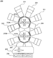
- FIG. 2A is a schematic configuration diagram of a substrate processing system 200 including an RF (Radio Frequency) sputtering film forming apparatus 300 according to the present embodiment.
- the substrate processing system 200 is a cluster-type apparatus, and includes an RF sputtering film forming apparatus 300, a plurality of substrate processing chambers 201, an oxidation processing chamber 208, a load lock chamber 204, and a transfer chamber 203.
- the plurality of substrate processing chambers 201 may perform the same processing on the substrate 10 or may perform different processing.
- the substrate 10 refers to a substrate in the manufacturing process, and includes the substrate 101 and a layer already formed thereon.
- the plurality of substrate processing chambers 201, the oxidation processing chamber 208, the load lock chamber 204, and the RF sputtering film forming apparatus 300 are connected to each other via the transfer chamber 203, and each connection portion can be opened and closed.
- a gate valve is provided.
- the transfer chamber 203 is provided with a transfer robot 207, and the transfer robot 207 moves the substrate between the substrate processing chamber 201, the load lock chamber 204, the RF sputtering film forming apparatus 300, and the oxidation processing chamber 208 according to a predetermined processing order. 10 is conveyed and a film forming process is performed.
- Each substrate processing chamber 201 and transfer chamber 203 are each provided with an exhaust pump, and the transfer robot 207 can transfer the substrate 10 between the chambers while maintaining a vacuum.
- An autoloader 205 for supplying the substrate 10 to the load lock chamber 204 is provided outside the load lock chamber 204 (side not connected to the transfer chamber 203). The autoloader 205 is configured to take out the substrates one by one from the external cassette 206 in which a plurality of substrates are stored on the atmosphere side and store them in the load lock chamber 204.
- the substrate processing system 200 may be a double-core substrate processing system including two transfer chambers 203A and 203B, as shown in FIG. 2B.
- An RF sputtering film forming apparatus 300, a plurality of substrate processing chambers 201 and an oxidation processing chamber 208 are connected to the transfer chamber 203A, and a load lock chamber 204 is connected to the transfer chamber 203B.
- the transfer robots 207A and 207B provided in the transfer chambers 203A and 203B, the substrate 10 is transferred between the substrate processing chamber 201, the load lock chamber 204, the RF sputtering film forming apparatus 300, and the oxidation processing chamber 208 according to a predetermined processing order. Is transported and a film forming process is performed.
- the RF sputtering film forming apparatus 300 includes two flat cathodes, and simultaneously sputtering two targets.
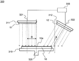
- FIG. 3A is a schematic cross-sectional view of the RF sputtering film forming apparatus 300 according to this embodiment.
- one cathode hereinafter referred to as the first cathode 311
- the other cathode hereinafter referred to as the second cathode 312
- the substrate 10 is disposed obliquely with respect to the film formation surface 10a.
- a first insulator target 11 and a second insulator target 12 are disposed on the first cathode 311 and the second cathode 312, respectively.
- a high-frequency power source 305 is electrically connected to the first cathode 311 and the second cathode 312, and the high-frequency power source 305 individually applies sputtering discharge power to the first cathode 311 and the second cathode 312.
- two insulator targets are simultaneously discharged at different cathode angles with respect to the film formation surface 10a of the substrate 10.
- an MgO target is used as the insulator target, but other oxides such as Al 2 O 3 may be used.
- the substrate 10 has a disk shape, is placed on the substrate holder 310, and is formed while rotating about the center of the substrate 10.
- the insulator targets 11 and 12 disposed on the first cathode 311 and the second cathode 312 are the same target.
- the first cathode 311 (first insulator target 11) arranged in parallel to the film formation surface 10 a of the substrate 10 has a normal line 321 passing through the center of the first cathode 311 passing through the center of the substrate 10.
- 320 central normal
- the normal line 321 passing through the center of the first cathode 311 (first insulator target 11) is disposed so as to pass through the film formation surface 10a of the substrate 10, but the outside of the substrate 10 is not affected. You may arrange
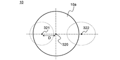
- 3B is a schematic plan view of the substrate 10 illustrated so as to correspond to the schematic plan view of FIG. 3A.
- the second cathode 312 (second insulator target 12) disposed obliquely with respect to the film formation surface 10 a of the substrate 10 has a normal line 322 passing through the center of the second cathode 312 passing through the center of the substrate 10. 321 and intersect at a predetermined angle ⁇ (predetermined cathode angle angle).
- the normal line 322 passing through the center of the second cathode 312 is arranged so as not to pass through the film formation surface 10 a of the substrate 10, but may be arranged so as to pass through the film formation surface 10 a of the substrate 10.
- the predetermined cathode angle angle ⁇ is set in the range of 10 degrees to 45 degrees.
- the power applied to the second insulator target 12 provided on the second cathode 312 is larger than the power applied to the first insulator target 11 provided on the first cathode 311.
- FIG. 10 is a flowchart showing steps included in the method for manufacturing a TMR element according to this embodiment.
- the substrate 10 on which a ferromagnetic layer is formed is prepared (step S101).
- the lower electrode 102, the Ta layer 103, the Ru layer 104, the stacked body 105, the Ta layer 106, and the CoFeB layer 107 that is a ferromagnetic layer are sequentially formed on the substrate 101.
- the first insulator target 11 is arranged in parallel to the film formation surface 10a of the substrate 10 (step S102).
- the MgO target as the first insulator target 11 is installed on the first cathode 311 arranged in parallel to the substrate 10.
- the second insulator target 12 is disposed obliquely with respect to the film formation surface 10a of the substrate 10 (step S103).
- the MgO target as the second insulator target 12 is installed on the second cathode 312 disposed with a predetermined cathode angle angle ⁇ with respect to the substrate 10. Note that the processing order of steps S101 to S103 is arbitrary.
- sputtering is simultaneously performed from the first insulator target 11 and the second insulator target 12 to form a tunnel barrier layer on the surface of the substrate 10 (S104).
- the discharge power is applied from the high frequency power source 305 to the MgO target installed on the first cathode 311 and the second cathode 312, so that the surface of the substrate 10, that is, on the CoFeB layer 107.
- an MgO layer 108 as a tunnel barrier layer is formed.
- the remaining layer of the TMR element is formed on the substrate 10.
- a CoFeB layer 109, a Ta layer 110, and an upper electrode 111 that are ferromagnetic layers are sequentially formed on the MgO layer 108 that is a tunnel barrier layer.
- the MTJ element 100 is formed using the substrate processing system 200 including the RF sputtering film forming apparatus 300 according to this embodiment shown in FIGS. 3A and 3B.
- the first insulator target 11 and the second insulator target 12 are arranged at two different angles, that is, parallel and oblique cathode angles.
- the MgO layer (tunnel barrier layer) 108 is formed by RF sputtering of two insulator targets simultaneously with parallel and oblique cathode angles.
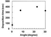
- FIG. 4 shows the cathode angle angle dependency of the deposition rate of the MgO layer 108 when the RF sputtering deposition apparatus 300 shown in FIGS. 3A and 3B is used.
- the horizontal axis is the cathode angle angle ⁇ , and the case of the cathode angle angle where the MgO target is arranged in parallel to the film formation surface 10a of the substrate 10 is 0 °.
- the vertical axis represents the film formation time until the reference film thickness is reached.
- the input power to each cathode is the same condition.
- the film formation speed is about 4 times faster than when the MgO target is arranged obliquely. This is presumably because the probability of adhesion to the substrate surface is higher when the targets are arranged in parallel.
- FIG. 5A and 5B show the cathode angle dependency of the RA and MR ratios when the RF sputtering film forming apparatus 300 according to the present embodiment is used.
- RA and MR ratios at six different locations from the center to the edge of the substrate 10 after film formation.
- the insulator target is arranged in parallel to the film formation surface 10a of the substrate 10 (cathode angle angle 0 °)
- the RA distribution and the MR distribution are deteriorated.
- the cathode angle angle ⁇ is increased, the RA distribution and the MR distribution tend to be improved.
- 6A and 6B show a case where the MgO target is arranged in parallel to the substrate 10 (cathode angle angle 0 °) and a case where the MgO target is arranged obliquely (cathode angle angle 22.5 °).
- the distribution of the MgO film thickness at the distance (152 mm, 194 mm, 244 mm) between the target and the substrate 10 is shown.
- the distance between the target and the substrate 10 was the distance from the center of the target surface to the center of the substrate.
- the MgO film thickness distribution has a convex shape having a peak at the center of the substrate surface.
- the standard deviations (1 ⁇ ) are 13.7%, 10.4%, and 8.4% at T / S distances of 152 mm, 194 mm, and 244 mm, respectively.
- the MgO film thickness distribution is concave with the peak at the center of the substrate surface.
- the standard deviations (1 ⁇ ) are 5.3%, 4.1%, and 3.4%, respectively, at T / S distances of 152 mm, 194 mm, and 244 mm.
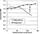
- FIG. 7A shows the case where the MgO target is arranged in parallel to the substrate 10 (cathode angle angle 0 °) and the case where the MgO target is arranged obliquely (cathode angle angle 22.5 °). Shows the RA distribution of the MgO film formed by the above.
- FIG. 7B shows the case where the MgO target is arranged parallel to the substrate 10 (cathode angle angle 0 °) and the case where the MgO target is arranged obliquely (cathode angle angle 22.5 °).
- the distribution of the MR ratio of the MgO film formed by the above is shown. RA and MR ratios are standardized with a center value of 1.
- the RA and MR distributions were convex with the peak at the center of the substrate surface.
- the MgO target was disposed obliquely (cathode angle angle 22.5 °)
- the RA and MR distributions were concave with peaks at the center of the substrate surface.
- Rp is a resistance value in a state in which the magnetizations of the fixed layer and the free layer are parallel (resistance is low).
- Rap is a resistance value in a state in which the magnetizations of the fixed layer and the free layer are antiparallel (high resistance).
- A is the cross-sectional area of the element (plane perpendicular to the current direction).
- the RA and MR ratio measurements were developed using Current In-Plane Tunneling (CIPT), a technology developed by IBM and Infineon Technologies, and CAPRES microscopic 12-point probe technology.
- CIPT Current In-Plane Tunneling
- measurement can be performed using a TMR element formed by processing a tunnel magnetoresistive film.
- the RA value measured by the CIPT measuring instrument is used.
- the CIPT method is a method in which the resistance in the direction perpendicular to the film surface of the TMR film is measured, and four probes are brought into contact with the surface of the magnetoresistive effect film to measure the resistance value.
- the resistance of the vertical MTJ film measured by the CIPT method is the horizontal resistance Rt above the MgO layer as the barrier layer, the horizontal resistance Rb below the MgO layer, and the resistance RA in the direction perpendicular to the MgO layer. This is the combined resistance.
- the lower and upper electrodes of the vertical MTJ film are metal layers having a low electrical resistance, thereby reducing the horizontal resistance of the upper and lower parts of the MgO layer and measuring the resistance RA in the vertical direction of the combined resistance. Accuracy can be increased. By using the CIPT method in this way, it is possible to measure the junction resistance RA and MR ratio.
- FIG. 8 is a diagram for explaining the film forming method according to the present embodiment. First, two comparative examples will be described as a comparison with the examples formed by the film forming method according to the present embodiment.
- Image A in FIG. 8 is a stacked image of the film (MgO) in the first comparative example.
- the first comparative example is an example of a two-stage film formation method in which a film of film quality B is formed after a film of film quality A is formed, and RA is uniform throughout.
- the film forming apparatus used in the first comparative example is the same as the RF sputtering film forming apparatus 300 in FIG. 3A, but the two insulator targets 11 and 12 are both arranged obliquely with respect to the substrate 10. The point is different.
- one of the two targets arranged obliquely with respect to the substrate 10 can form a film of the film quality A with one target, and a film of the film quality B can be formed with the other target. After film formation, film quality B was formed.
- Image B in FIG. 8 is a stacked image of the film (MgO) in the second comparative example.
- the second comparative example is an example in which the film quality A and the film quality B are simultaneously formed using the same apparatus as the first comparative example.
- Overall, RA is equal.
- the two targets are both arranged obliquely with respect to the substrate 10, the film formation rate is slow and it is difficult to increase the throughput.
- the second comparative example can obtain a better RA distribution than the example of the present embodiment described later.
- the power input to the first insulator target is the same as the power input to the second insulator target, but the same applies even if a difference is applied to the applied power. As a result.
- An image C in FIG. 8 is a laminated image of the film (MgO) in the present embodiment.
- the film was formed by a film forming process in which two insulator targets were simultaneously discharged at different cathode angles with respect to the substrate 10.
- the two insulator targets include an insulator target (first insulator target 11) in which an MgO target is disposed in parallel to the film formation surface 10 a of the substrate 10, and a substrate 10.
- the first cathode 311 in which the MgO target is arranged in parallel increases the deposition rate of the MgO film
- the power input to the first insulator target 11 is lower than the power input to the second insulator target 12.
- the power input to the first insulator target 11 is 230 W
- the power input to the second insulator target 12 is 800 W.
- FIG. 9A shows the results of RA when the MgO layer (tunnel barrier layer) 108 is formed by the method of Comparative Example 2 and the method of this example.
- FIG. 9B shows the MR ratio results when the MgO layer (tunnel barrier layer) 108 is formed by the method of Comparative Example 2 and the method of this example.
- the RA distribution of this example is better than the RA distribution of Comparative Example 2.
- the standard deviation (1 ⁇ ) of the RA distribution of Comparative Example 2 is 4.5%
- the standard deviation (1 ⁇ ) of the RA distribution of this example is 1.9%.
- the MR ratio of the film according to the present example is higher than the MR ratio of the film according to the comparative example 2, and the variation in the MR ratio of the present example is larger than the variation in the MR ratio of the comparative example 2. It is getting smaller.
- the standard deviation (1 ⁇ ) of the MR ratio distribution of Comparative Example 2 is 6.0%, and the standard deviation (1 ⁇ ) of the MR ratio distribution of this example is 2.5%. This is presumably because the in-plane film quality became uniform.
- the first cathode 311 in which the MgO target is arranged in parallel has a higher deposition rate of the MgO film than the second cathode 312 in which the MgO target is arranged obliquely.
- the power applied to the first cathode 311 is set lower than the power applied to the second cathode 312 (second insulator target 12). That is, the film thickness distribution, RA and MR ratio distribution can be adjusted by changing the power applied to each target.
- a large electric power was applied to the cathode on which the oblique MgO target was disposed. In this method, it is presumed that the crystallinity of the MgO film was deteriorated due to the high energy of the sputtered MgO particles.
- the MgO particles sputtered from the first cathode 311 in which the MgO target is arranged in parallel have a good adhesion probability on the substrate surface, and thus the film is formed without applying large electric power to the MgO target. Speed can be increased. Therefore, it is considered that the crystallinity of the MgO film can be improved because the energy of the MgO particles is low.
- Perpendicular Magnetoresistive Element 107 Reference Layer (Ferromagnetic Layer) 108 Tunnel barrier layer 109 Free layer (ferromagnetic layer) 200 substrate processing system 201 substrate processing chamber 203 transfer chamber 204 load lock chamber 300 RF sputtering film formation apparatus 10 substrate 10a film formation surface 11 first insulator target 12 second insulator target 311 first cathode 312 second cathode 320 Substrate center normal 321 First cathode center normal 322 Second cathode center normal
Landscapes
- Chemical & Material Sciences (AREA)
- Engineering & Computer Science (AREA)
- Chemical Kinetics & Catalysis (AREA)
- Materials Engineering (AREA)
- Mechanical Engineering (AREA)
- Metallurgy (AREA)
- Organic Chemistry (AREA)
- Manufacturing & Machinery (AREA)
- Hall/Mr Elements (AREA)
- Mram Or Spin Memory Techniques (AREA)
Abstract
本発明の一実施形態に係るトンネル磁気抵抗効果素子の製造方法は、強磁性層が形成された基板を用意する工程と、第1の絶縁物ターゲットを基板の成膜面に対して平行に配置する工程と、第2の絶縁物ターゲットを基板の成膜面に対して所定のカソードアングル角度を有して配置する工程と、第1および第2の絶縁物ターゲットから同時にスパッタリングし、基板の表面にトンネルバリア層の形成を行う工程と、を有することを特徴とする。
Description
本発明は、磁気抵抗効果素子の製造方法および装置に係り、特にMRAMに用いられるTMR素子に好適な製造方法および装置に関する。
トンネル磁気抵抗効果(TMR:Tunnel Magneto Resistance effect)は、磁場によって電気抵抗が変化する現象であり、トンネル磁気抵抗効果(TMR)素子は、このTMR効果を利用した素子である。面内磁化型のTMR素子は、主にハードディスクドライブに用いられてきた。面内磁化型のTMR素子では、フリー層とリファレンス層の磁化方向が積層膜の面内方向に磁化回転する。近年、集積化磁気メモリであるMRAM(Magnetic Random Access Memory)が注目を集めている。MRAMに用いられるTMR素子としては、非特許文献1に示される垂直磁化型のMTJ(Magnetic Tunnel Junction:磁気トンネル接合)素子が存在する。垂直磁化型のMTJ素子は、フリー層(磁化自由層)、トンネルバリア層、およびリファレンス層(磁化固定層)が積層された構造、すなわち2つの強磁性層の間にトンネルバリア層が配された構造を含み、フリー層およびリファレンス層の磁化方向はそれぞれ積層方向と平行になっている。
TMR素子の製造においては、所望の成膜材料から成るターゲットをスパッタリングすることにより、対向する基板上に成膜するスパッタリング(以下単にスパッタともいう)法が広く用いられている。TMR素子に用いられるトンネルバリア層の製造方法として、特許文献1には、酸化物ターゲットに対してRFスパッタを行うことで酸化膜を成膜する方法が開示され、特許文献2には、金属膜を成膜した後に酸化処理を施すことで酸化膜を形成する方法が開示されている。
磁気抵抗効果素子を用いたMRAMデバイスの特性の向上のためには、MR比(磁気抵抗比)を高くすることが重要である。また、生産コストを低減するため、基板面内の均一性を良くすること、スループットを速くすることが重要である。非特許文献1に記載のCoFeB/MgO/CoFeBからなる積層構造は100%を超える高いMR比を示すことが知られている。この積層構造を短時間で且つ基板面内に均一に成膜する方法が期待されている。
D. C. Worledge et al., "Spin torque switching of perpendicular Ta|CoFeB|MgO-based magnetic tunnel junctions", Appl. Phys. Lett. 98, 2011, 022501
TMR素子を用いたデバイスにおいて、より高い出力信号を得るためには、高いMR比を有するTMR素子を製造する必要がある。特にトンネルバリア層の状態はMR比に大きく影響する。特許文献1に記載される酸化物ターゲットを用いて酸化膜を形成する方法を用いてTMR素子を製造する場合、特許文献2に記載される金属膜の酸化によって酸化膜を形成する方法を用いてTMR素子を製造する場合に比べて、高いMR比が得られる傾向にある。しかしながら、特許文献1に記載の方法を用いて酸化膜の成膜処理を施した場合、特許文献2に記載の方法を用いて酸化膜を形成した場合に比べて、基板面内の各点、特に基板の中心から外周にかけて、電気抵抗値のばらつきが大きい傾向にある。このような電気抵抗値のばらつきは、1枚の基板から得られる磁気抵抗効果素子間の特性のばらつきの原因となり、歩留まりを悪化させるため、可能な限り低減されることが望ましい。また、生産コストを低減するためには、スループット(1時間当たりの基板処理枚数)を速くすることが求められている。
本発明は、上述した課題を解決すべく為されたものであり、酸化物ターゲットを用いて基板にスパッタ法により成膜処理を行う場合に、高いMR比を有し、基板面内の電気抵抗値のばらつきを低減し、さらにスループットを速くすることを目的とする。
本発明の一態様に係るトンネル磁気抵抗効果素子の製造方法は、強磁性層が形成された基板を用意する工程と、第1の絶縁物ターゲットを前記基板の成膜面に対して平行に配置する工程と、第2の絶縁物ターゲットを前記基板の成膜面に対して所定のカソードアングル角度を有して配置する工程と、前記第1および第2の絶縁物ターゲットから同時にスパッタリングし、前記基板の表面にトンネルバリア層の形成を行う工程と、を有することを特徴とする。
本発明の一態様に係るスパッタリング成膜装置は、基板に対して平行に配置され、第1の絶縁物ターゲットが設けられた第1カソードと、前記基板に対して斜めに配置され、第2の絶縁物ターゲットが設けられた第2カソードと、を有し、前記基板上に、2つの強磁性層の間にトンネルバリア層が配されたトンネル磁気抵抗効果素子の製造のためのスパッタリング成膜装置であって、前記第1カソードは、前記第1カソードの中心を通る法線が前記基板の中心を通る法線と平行であり、前記第1カソードの中心を通る法線が、前記基板の中心を通る法線から離間して配置されており、前記第2カソードは、前記第2カソードの中心を通る法線が前記基板の中心を通る法線と一致せず、所定の角度θで交わっていることを特徴とする。
本発明によれば、酸化物ターゲットを用いて基板にスパッタ法により成膜処理を行う場合に、高いMR比を有し、基板面内の電気抵抗値のばらつきを低減し、スループットを速くすることが可能となる。また、酸化物ターゲットを用いて酸化膜の形成を行うため、金属膜の酸化によって酸化膜を形成する場合に比べて、高いMR比を得ることが可能となる。
以下、図面を参照して、本発明の実施の形態を説明するが、本発明は本実施形態に限定されるものではない。なお、以下で説明する図面で、同機能を有するものは同一符号を付け、その繰り返しの説明は省略することもある。
以下に、本発明を適用可能なTMR素子の構造の例を示す。
(垂直磁化型トンネル磁気抵抗効果素子の構造の説明)
図1は、本実施形態に係る成膜方法を行う例示的なMTJ(Magnetic Tunnel Junction:磁気トンネル接合)素子100の構成を示す模式図である。MTJ素子は、例えばMRAM(Magnetic Random Access Memory)、磁気センサ等に用いられる。
(垂直磁化型トンネル磁気抵抗効果素子の構造の説明)
図1は、本実施形態に係る成膜方法を行う例示的なMTJ(Magnetic Tunnel Junction:磁気トンネル接合)素子100の構成を示す模式図である。MTJ素子は、例えばMRAM(Magnetic Random Access Memory)、磁気センサ等に用いられる。
MTJ素子100は、垂直磁化型MTJ素子(p-MTJ素子)である。MTJ素子100は、基板101上に、下部電極102と、Ta層(シード層)103と、Ru層(シード層)104と、Co層とPt層とを交互に所定の数Nだけ積層した積層体105(ピン層)と、Ta層(スペーサー層)106と、リファレンス層(磁化固定層)としてのCoFeB層107と、MgO層(トンネルバリア層)108と、フリー層(磁化自由層)としてのCoFeB層109と、Ta層(キャップ層)110と、上部電極111とを順に備える。MTJ素子100としてはここに示した構成に限られず、垂直磁化型MTJ素子の機能を損なわない範囲で層の増減、各層の構成材料の変更、上下の積層順の逆転等の任意の変更を行った構成を用いることができる。
(本実施形態に係るTMR素子の製造方法の説明)
図2Aは、本実施形態に係るRF(Radio Frequency)スパッタリング成膜装置300を備える基板処理システム200の概略構成図である。基板処理システム200はクラスタ型の装置であり、RFスパッタリング成膜装置300と、複数の基板処理チャンバ201と、酸化処理チャンバ208と、ロードロックチャンバ204と、搬送チャンバ203とを備えている。複数の基板処理チャンバ201は、基板10に対して同一の処理を行うものであってもよく、または異なる処理を行うものであってもよい。以下の説明において、基板10は製造過程にある基板のことを指し、基板101とその上に既に形成された層を含む。
図2Aは、本実施形態に係るRF(Radio Frequency)スパッタリング成膜装置300を備える基板処理システム200の概略構成図である。基板処理システム200はクラスタ型の装置であり、RFスパッタリング成膜装置300と、複数の基板処理チャンバ201と、酸化処理チャンバ208と、ロードロックチャンバ204と、搬送チャンバ203とを備えている。複数の基板処理チャンバ201は、基板10に対して同一の処理を行うものであってもよく、または異なる処理を行うものであってもよい。以下の説明において、基板10は製造過程にある基板のことを指し、基板101とその上に既に形成された層を含む。
複数の基板処理チャンバ201と、酸化処理チャンバ208と、ロードロックチャンバ204と、RFスパッタリング成膜装置300とは、搬送チャンバ203を介して互いに接続されており、それぞれの接続部分には開閉可能なゲートバルブが設けられている。搬送チャンバ203には搬送ロボット207が設けられており、搬送ロボット207によって各基板処理チャンバ201、ロードロックチャンバ204、RFスパッタリング成膜装置300、酸化処理チャンバ208の間で、所定の処理順に従って基板10が搬送され、成膜処理が行われる。各基板処理チャンバ201、搬送チャンバ203にはそれぞれ排気ポンプが設けられており、搬送ロボット207は、真空を保ったままチャンバ間で基板10を搬送可能である。ロードロックチャンバ204の外側(搬送チャンバ203に接続されていない側)には、基板10をロードロックチャンバ204に供給するためのオートローダ205が設けられている。オートローダ205は、大気側において複数の基板が収納されている外部カセット206から基板を一枚ずつ取り出し、ロードロックチャンバ204内に収容するように構成されている。
基板処理システム200は、図2Bに示されるように、2つの搬送チャンバ203A、203Bを備えたダブルコアの基板処理システムであってもよい。搬送チャンバ203Aには、RFスパッタリング成膜装置300、複数の基板処理チャンバ201、酸化処理チャンバ208が接続され、搬送チャンバ203Bには、ロードロックチャンバ204が接続されている。搬送チャンバ203A、203Bにそれぞれ設けられた搬送ロボット207A、207Bにより、各基板処理チャンバ201、ロードロックチャンバ204、RFスパッタリング成膜装置300、酸化処理チャンバ208の間で、所定の処理順に従って基板10が搬送され、成膜処理が行われる。
次に図3A、図3Bを用いて本実施形態に係るRFスパッタリング成膜装置300について説明する。RFスパッタリング成膜装置300は、2つの平板状のカソードを備えており、同時に2つのターゲットをスパッタリングする。
図3Aは、本実施形態に係るRFスパッタリング成膜装置300の概略断面図である。RFスパッタリング成膜装置300において、1つのカソード(以下、第1カソード311)は、基板10の成膜面10aに対して平行に配置され、もう1つのカソード(以下、第2カソード312)は、基板10の成膜面10aに対して斜めに配置されている。第1カソード311、第2カソード312には、それぞれ第1の絶縁物ターゲット11、第2の絶縁物ターゲット12が配置される。第1カソード311、第2カソード312には、高周波電源305が電気的に接続され、高周波電源305は、第1カソード311、第2カソード312に対して、個別にスパッタ放電用電力を印加する。本実施形態では、基板10の成膜面10aに対して異なるカソードアングルで、同時に2つの絶縁物ターゲットを放電する。この方法により、従来の方法に比べて絶縁膜の成膜速度すなわちスループットを速くすること、さらに基板面内のRA、MR比のばらつきを低減することが可能となる。なお、絶縁物ターゲットとして本実施形態ではMgOターゲットを用いるが、Al2O3などの他の酸化物を用いてもよい。基板10は円板状であり、基板ホルダー310に載置され、基板10の中心を軸として回転しながら成膜される。第1カソード311、第2カソード312にそれぞれ配置される絶縁物ターゲット11、12は、同一のターゲットである。
基板10の成膜面10aに対して平行に配置された第1カソード311(第1の絶縁物ターゲット11)は、第1カソード311の中心を通る法線321が基板10の中心を通る法線320(中心法線)と平行であるが、基板10の中心法線から距離Dだけ離間して配置(オフセット配置)されている。本実施形態では、第1カソード311(第1の絶縁物ターゲット11)の中心を通る法線321は、基板10の成膜面10aを通過するように配置されているが、基板10の外側を通過するように、すなわち基板10の成膜面10aを通過しないように配置してもよい。なお、第1カソード311の中心を通る法線321と基板10の中心を通る法線320は実質的に平行であればよく、数度の傾きは実質的に平行な関係に含まれる。図3Bは、図3Aの概略平面図に対応するように図示した基板10の概略平面図である。
基板10の成膜面10aに対して斜めに配置された第2カソード312(第2の絶縁物ターゲット12)は、第2カソード312の中心を通る法線322が基板10の中心を通る法線321と一致せず、また、所定の角度θ(所定のカソードアングル角度)で交わっている。本実施形態では、第2カソード312の中心を通る法線322は基板10の成膜面10aを通過しないように配置されているが、基板10の成膜面10aを通過する配置でもよい。所定のカソードアングル角度θは、10度~45度の範囲に設定される。
また、第2カソード312に設けられた第2の絶縁物ターゲット12に印加される電力は、第1カソード311に設けられた第1の絶縁物ターゲット11に印加される電力よりも大きい。
図10は、本実施形態に係るTMR素子の製造方法に含まれる工程を示すフローチャートである。まず、基板処理システム200において、強磁性層が形成された基板10を用意する(ステップS101)。例えば、複数の基板処理チャンバ201において、基板101上に下部電極102、Ta層103、Ru層104、積層体105、Ta層106、および強磁性層であるCoFeB層107を順に成膜する。次に、第1の絶縁物ターゲット11を基板10の成膜面10aに対して平行に配置する(ステップS102)。例えば、RFスパッタリング成膜装置300において、第1の絶縁物ターゲット11としてのMgOターゲットを、基板10に対して平行に配置された第1カソード311に設置する。続いて、第2の絶縁物ターゲット12を基板10の成膜面10aに対して斜めに配置する(ステップS103)。例えば、RFスパッタリング成膜装置300において、第2の絶縁物ターゲット12としてのMgOターゲットを、基板10に対して所定のカソードアングル角度θを有して配置された第2カソード312に設置する。なお、上記ステップS101~S103の処理順は任意である。
次に、第1の絶縁物ターゲット11および第2の絶縁物ターゲット12から同時にスパッタリングし、基板10の表面にトンネルバリア層を形成する(S104)。例えば、RFスパッタリング成膜装置300において、第1カソード311および第2カソード312に設置されたMgOターゲットに高周波電源305から放電用電力を印加することにより、基板10の表面すなわちCoFeB層107の上に、トンネルバリア層であるMgO層108を成膜する。
トンネルバリア層を形成した後、基板10にTMR素子の残りの層を形成する。例えば、基板処理システム200の複数の基板処理チャンバ201において、トンネルバリア層であるMgO層108の上に、強磁性層であるCoFeB層109、Ta層110、上部電極111を順に成膜する。
上述したRA、MR分布のばらつきを低減するために、図3A、図3Bに示した本実施形態に係るRFスパッタリング成膜装置300を備える基板処理システム200を用いてMTJ素子100を成膜する。本実施形態では2つの異なる角度、すなわち平行と斜めのカソードアングルに第1の絶縁物ターゲット11、第2の絶縁物ターゲット12をそれぞれ配置する。そして、平行と斜めのカソードアングルで同時に2つの絶縁物ターゲットをRFスパッタリングすることによりMgO層(トンネルバリア層)108の成膜を行う。
図4に、図3Aおよび図3Bに示したRFスパッタリング成膜装置300を用いた場合のMgO層108の成膜速度のカソードアングル角度依存性を示す。横軸はカソードアングル角度θであり、基板10の成膜面10aに対して平行にMgOターゲットを配置したカソードアングル角度の場合を0°としている。縦軸は基準の膜厚に達するまでの成膜時間である。各カソードへの入力パワーは同じ条件である。
基板10の成膜面10aに対して平行にMgOターゲットを配置した場合(カソードアングル角度0°)は、斜めにMgOターゲットを配置した場合よりも成膜速度は最大で約4倍速くなる。これは、平行にターゲットを配置した場合の方が、基板表面への付着確率が高くなるためと考えられる。
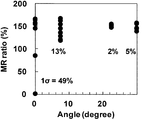
図5A、図5Bに本実施形態に係るRFスパッタリング成膜装置300を用いた場合のRAとMR比のカソードアングル角度依存性を示す。成膜後の基板10の中心から縁に向かって6箇所の異なる場所におけるRAとMR比である。基板10の成膜面10aに対して平行に絶縁物ターゲットを配置した場合(カソードアングル角度0°)は、RA分布、MR分布は悪くなる。また、カソードアングル角度θを大きくすると、RA分布、MR分布は良くなる傾向が見られる。
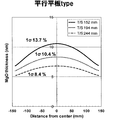
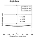
図6A、図6Bは、基板10に対して平行にMgOターゲットを配置した場合(カソードアングル角度0°)と、斜めにMgOターゲットを配置した場合(カソードアングル角度22.5°)において、それぞれのターゲットと基板10の距離(152mm、194mm、244mm)におけるMgO膜厚の分布を示す。ターゲットと基板10の距離(T/S距離)は、ターゲット表面の中心から基板中心までの距離とした。
図6Aに示されるように、測定したすべてのT/S距離で、平行にMgOターゲットを配置した場合においては、MgO膜厚分布は基板面の中心をピークとする凸型となる。標準偏差(1σ)は、T/S距離152mm、194mm、244mmにおいて、それぞれ13.7%、10.4%、8.4%である。また、図6Bに示されるように、斜めにMgOターゲットを配置した場合においては、MgO膜厚分布は基板面の中心をピークとする凹型となる。標準偏差(1σ)は、T/S距離152mm、194mm、244mmにおいて、それぞれ5.3%、4.1%、3.4%である。
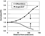
図7Aは、基板10に対して平行にMgOターゲットを配置した場合(カソードアングル角度0°)と、斜めにMgOターゲットを配置した場合(カソードアングル角度22.5°)の場合において、それぞれのターゲットにより成膜されるMgO膜のRA分布を示す。また、図7Bは、基板10に対して平行にMgOターゲットを配置した場合(カソードアングル角度0°)と、斜めにMgOターゲットを配置した場合(カソードアングル角度22.5°)において、それぞれのターゲットにより成膜されるMgO膜のMR比の分布を示す。RA、MR比は、中心値を1として規格化している。平行にMgOターゲットを配置した場合(オフセット距離65mm)においては、RA、MR分布は基板面の中心をピークとする凸型となった。また、斜めにMgOターゲットを配置した場合(カソードアングル角度22.5°)においては、RA、MR分布は基板面の中心をピークとする凹型となった。
ここで、本実施形態の説明においても用いたRA、MR比について説明を行う。RAは接合抵抗値を意味し、RA=Rp×A(Ωμm2)で定義され、MR比はTMR効果の大きさを示し、(Rap-Rp)/Rpで定義される。ここで、Rpは固定層と自由層の磁化が平行な(抵抗が低い)状態における抵抗値である。Rapは固定層と自由層の磁化が反平行な(抵抗が高い)状態における抵抗値である。Aは素子の断面積(電流方向に垂直な面)である。RA、MR比の測定には、米IBM社と独Infineon Technologies社が開発した技術であるCurrent In-Plane Tunneling (CIPT)と、CAPRES社のマイクロスコピック12ポイントプローブの技術とを用いて開発された測定器で測定する方法を用いる。測定の対象としては、トンネル磁気抵抗膜を加工して形成されたTMR素子を用いて測定することができる。あるいは、より簡易的に測定できるCIPT測定器で測定したRA値を用いてもよい。本発明では、CIPT測定器で測定したRA値を用いている。CIPT法は、TMR膜の膜面に垂直方向の抵抗を測定し、磁気抵抗効果膜の表面に4本のプローブを接触させて抵抗値を測定する方法である。例として、図1に示す垂直MTJ膜を用いた場合について説明する。CIPT法によって測定される垂直MTJ膜の抵抗は、バリア層であるMgO層の上部の水平方向の抵抗Rtと、MgO層の下部の水平方向の抵抗Rbと、MgO層に垂直な方向の抵抗RAの合成抵抗となる。垂直MTJ膜の下部と上部の電極は、電気抵抗が小さい金属層とすることにより、MgO層の上部と下部の水平方向の抵抗を低減させ、合成抵抗のうちの垂直な方向の抵抗RAの測定精度を高めることができる。この様にCIPT法を用いることにより、接合抵抗値であるRAとMR比が測定可能となる。
図8は、本実施形態に係る成膜方法について説明するための図である。まず、本実施形態に係る成膜方法にて成膜した実施例との比較として、2つの比較例について説明する。
<第1の比較例>
図8のイメージAは、第1の比較例での膜(MgO)の積層イメージである。第1の比較例は、膜質Aの膜を成膜した後、膜質Bの膜を成膜し、全体的にRAが均等になる2段階成膜方法の例である。第1の比較例で使用する成膜装置は、図3AのRFスパッタリング成膜装置300と同様のものであるが、基板10に対して2つの絶縁物ターゲット11、12を両方とも斜めに配置した点が異なる。この装置を使って、基板10に対して斜めに配置した2つのターゲットのうち、一方のターゲットで膜質Aの膜を成膜でき、他方のターゲットで膜質Bの膜を成膜できるため、膜質Aを成膜した後、膜質Bを成膜した。異なる2つの膜質を得るためには、例えばMgO膜を成膜する圧力やターゲットと基板10の距離を変える方法がある。膜質Aの膜と、膜質Bの膜の成膜時間を別々に設定できるため見掛けのRAは全体的に均等にできる。しかし、この方法では、成膜装置内の圧力変更や基板距離の制御に時間がかかってしまう。また、全体的にRAは均等になっているが膜厚が薄くなると制御が困難である。2つのターゲットはいずれも基板10に対して斜めに配置されているため、成膜速度が遅く、スループットを上げることは困難である。
図8のイメージAは、第1の比較例での膜(MgO)の積層イメージである。第1の比較例は、膜質Aの膜を成膜した後、膜質Bの膜を成膜し、全体的にRAが均等になる2段階成膜方法の例である。第1の比較例で使用する成膜装置は、図3AのRFスパッタリング成膜装置300と同様のものであるが、基板10に対して2つの絶縁物ターゲット11、12を両方とも斜めに配置した点が異なる。この装置を使って、基板10に対して斜めに配置した2つのターゲットのうち、一方のターゲットで膜質Aの膜を成膜でき、他方のターゲットで膜質Bの膜を成膜できるため、膜質Aを成膜した後、膜質Bを成膜した。異なる2つの膜質を得るためには、例えばMgO膜を成膜する圧力やターゲットと基板10の距離を変える方法がある。膜質Aの膜と、膜質Bの膜の成膜時間を別々に設定できるため見掛けのRAは全体的に均等にできる。しかし、この方法では、成膜装置内の圧力変更や基板距離の制御に時間がかかってしまう。また、全体的にRAは均等になっているが膜厚が薄くなると制御が困難である。2つのターゲットはいずれも基板10に対して斜めに配置されているため、成膜速度が遅く、スループットを上げることは困難である。
<第2の比較例>
図8のイメージBは、第2の比較例での膜(MgO)の積層イメージである。第2の比較例は、第1の比較例と同一の装置を使って、膜質Aの成膜と膜質Bの成膜を同時に行った例である。全体的にRAは均等になっている。しかし、2つのターゲットはいずれも基板10に対して斜めに配置されているため、成膜速度が遅く、スループットを上げることは困難である。さらに、図9A、図9Bに示すように、第2の比較例は後述する本実施形態の実施例よりも良好なRA分布が得られる。なお、第2の比較例では、第1の絶縁物ターゲットに投入される電力は、第2の絶縁物ターゲットに投入される電力と同じとしたが、印加する電力に差を設けても同様の結果となった。
図8のイメージBは、第2の比較例での膜(MgO)の積層イメージである。第2の比較例は、第1の比較例と同一の装置を使って、膜質Aの成膜と膜質Bの成膜を同時に行った例である。全体的にRAは均等になっている。しかし、2つのターゲットはいずれも基板10に対して斜めに配置されているため、成膜速度が遅く、スループットを上げることは困難である。さらに、図9A、図9Bに示すように、第2の比較例は後述する本実施形態の実施例よりも良好なRA分布が得られる。なお、第2の比較例では、第1の絶縁物ターゲットに投入される電力は、第2の絶縁物ターゲットに投入される電力と同じとしたが、印加する電力に差を設けても同様の結果となった。
<本実施例>
図8のイメージCは、本実施例での膜(MgO)の積層イメージである。本実施例では、基板10に対して異なるカソードアングルで同時に2つの絶縁物ターゲットを放電する成膜過程により成膜した。2つの絶縁物ターゲットは、図3Aに示すように、基板10の成膜面10aに対して平行にMgOターゲットを配置された絶縁物ターゲット(第1の絶縁物ターゲット11)と、基板10の成膜面10aに対して所定のカソードアングル角度θを有して配置された絶縁物ターゲット(第2の絶縁物ターゲット12)である。これにより、平行にMgOターゲットを配置した第1カソード311はMgO膜の成膜速度を速くし、斜めにMgOターゲットを配置した第2カソード312はMgO膜の分布を改善し、同時に膜質の異なるMgO膜をRFスパッタリングすることにより、基板面内に均一な膜質のMgO膜を高速に成膜することが可能となる。なお、第1の絶縁物ターゲット11に投入される電力は、第2の絶縁物ターゲット12に投入される電力よりも低い。例えば、第1の絶縁物ターゲット11に投入される電力は230Wであり、第2の絶縁物ターゲット12に投入される電力は800Wである。
図8のイメージCは、本実施例での膜(MgO)の積層イメージである。本実施例では、基板10に対して異なるカソードアングルで同時に2つの絶縁物ターゲットを放電する成膜過程により成膜した。2つの絶縁物ターゲットは、図3Aに示すように、基板10の成膜面10aに対して平行にMgOターゲットを配置された絶縁物ターゲット(第1の絶縁物ターゲット11)と、基板10の成膜面10aに対して所定のカソードアングル角度θを有して配置された絶縁物ターゲット(第2の絶縁物ターゲット12)である。これにより、平行にMgOターゲットを配置した第1カソード311はMgO膜の成膜速度を速くし、斜めにMgOターゲットを配置した第2カソード312はMgO膜の分布を改善し、同時に膜質の異なるMgO膜をRFスパッタリングすることにより、基板面内に均一な膜質のMgO膜を高速に成膜することが可能となる。なお、第1の絶縁物ターゲット11に投入される電力は、第2の絶縁物ターゲット12に投入される電力よりも低い。例えば、第1の絶縁物ターゲット11に投入される電力は230Wであり、第2の絶縁物ターゲット12に投入される電力は800Wである。
図9Aに比較例2の方法と本実施例の方法によりMgO層(トンネルバリア層)108の成膜を行った場合のRAの結果を示す。また、図9Bに比較例2の方法と本実施例の方法によりMgO層(トンネルバリア層)108の成膜を行った場合のMR比の結果を示す。本実施例のRA分布は、比較例2のRA分布に比べて良くなっている。比較例2のRA分布の標準偏差(1σ)は4.5%であり、本実施例のRA分布の標準偏差(1σ)は1.9%である。また、本実施例による膜のMR比は、比較例2による膜のMR比に比べて高くなっており、さらに本実施例のMR比のばらつきは、比較例2のMR比のばらつきに比べて小さくなっている。比較例2のMR比分布の標準偏差(1σ)は6.0%であり、本実施例の方MR比分布の標準偏差(1σ)は2.5%である。これは、面内の膜質が均一になったためと考えられる。さらに、本実施例の方法では、平行にMgOターゲットを配置した第1カソード311は、斜めにMgOターゲットを配置した第2カソード312と比べて、MgO膜の成膜速度が速い。そのため、第1カソード311(第1の絶縁物ターゲット11)に印加する電力を第2カソード312(第2の絶縁物ターゲット12)に印加する電力よりも低くしている。すなわち、それぞれのターゲットに印加する電力を変えることにより、膜厚分布、RA及びMR比分布を調整することができる。比較例2の方法では、成膜速度を速めるためには、斜めのMgOターゲットを配置したカソードに大きな電力を投入していた。この方法では、スパッタされたMgO粒子のエネルギーが高いためにMgO膜の結晶性を劣化させていたと推測される。本実施形態に係る方法では、平行にMgOターゲットを配置した第1カソード311からスパッタされたMgO粒子は、基板表面での付着確率が良いため、MgOターゲットに大きな電力を投入しなくても成膜速度を速くできる。よって、MgO粒子のエネルギーが低いことからMgO膜の結晶性を向上できると考えられる。
100 垂直磁化型磁気抵抗効果素子
107 リファレンス層(強磁性層)
108 トンネルバリア層
109 フリー層(強磁性層)
200 基板処理システム
201 基板処理チャンバ
203 搬送チャンバ
204 ロードロックチャンバ
300 RFスパッタリング成膜装置
10 基板
10a 成膜面
11 第1の絶縁物ターゲット
12 第2の絶縁物ターゲット
311 第1カソード
312 第2カソード
320 基板の中心法線
321 第1カソードの中心法線
322 第2カソードの中心法線
107 リファレンス層(強磁性層)
108 トンネルバリア層
109 フリー層(強磁性層)
200 基板処理システム
201 基板処理チャンバ
203 搬送チャンバ
204 ロードロックチャンバ
300 RFスパッタリング成膜装置
10 基板
10a 成膜面
11 第1の絶縁物ターゲット
12 第2の絶縁物ターゲット
311 第1カソード
312 第2カソード
320 基板の中心法線
321 第1カソードの中心法線
322 第2カソードの中心法線
Claims (6)
- 強磁性層が形成された基板を用意する工程と、
第1の絶縁物ターゲットを前記基板の成膜面に対して平行に配置する工程と、
第2の絶縁物ターゲットを前記基板の成膜面に対して所定のカソードアングル角度を有して配置する工程と、
前記第1および第2の絶縁物ターゲットから同時にスパッタリングし、前記基板の表面にトンネルバリア層の形成を行う工程と、
を有することを特徴とするトンネル磁気抵抗効果素子の製造方法。 - 前記第1の絶縁物ターゲットに投入される電力は、前記第2の絶縁物ターゲットに投入される電力よりも低いことを特徴とする請求項1に記載のトンネル磁気抵抗効果素子の製造方法。
- 前記第1の絶縁物ターゲットは、前記基板の中心法線から離間して配置(オフセット配置)されることを特徴とする請求項1又は2に記載のトンネル磁気抵抗効果素子の製造方法。
- 前記第1の絶縁物ターゲットと前記第2の絶縁物ターゲットは同一のターゲットであることを特徴とする請求項1乃至3のいずれか1項に記載のトンネル磁気抵抗効果素子の製造方法。
- 基板に対して平行に配置され、第1の絶縁物ターゲットが設けられた第1カソードと、
前記基板に対して斜めに配置され、第2の絶縁物ターゲットが設けられた第2カソードと、を有し、
前記基板上に、2つの強磁性層の間にトンネルバリア層が配されたトンネル磁気抵抗効果素子の製造のためのスパッタリング成膜装置であって、
前記第1カソードは、前記第1カソードの中心を通る法線が前記基板の中心を通る法線と平行であり、前記第1カソードの中心を通る法線が、前記基板の中心を通る法線から離間して配置されており、
前記第2カソードは、前記第2カソードの中心を通る法線が前記基板の中心を通る法線と一致せず、所定の角度θで交わっていることを特徴とするスパッタリング成膜装置。 - 前記第1カソードの中心を通る法線は、前記基板の成膜面を通過するように配置されており、前記第2カソードの中心を通る法線は、前記基板の成膜面を通過しないように配置されていることを特徴とする請求項5に記載のスパッタリング成膜装置。
Priority Applications (1)
| Application Number | Priority Date | Filing Date | Title |
|---|---|---|---|
| PCT/JP2015/006056 WO2017098537A1 (ja) | 2015-12-07 | 2015-12-07 | 磁気抵抗効果素子の製造方法および装置 |
Applications Claiming Priority (1)
| Application Number | Priority Date | Filing Date | Title |
|---|---|---|---|
| PCT/JP2015/006056 WO2017098537A1 (ja) | 2015-12-07 | 2015-12-07 | 磁気抵抗効果素子の製造方法および装置 |
Publications (1)
| Publication Number | Publication Date |
|---|---|
| WO2017098537A1 true WO2017098537A1 (ja) | 2017-06-15 |
Family
ID=59012792
Family Applications (1)
| Application Number | Title | Priority Date | Filing Date |
|---|---|---|---|
| PCT/JP2015/006056 Ceased WO2017098537A1 (ja) | 2015-12-07 | 2015-12-07 | 磁気抵抗効果素子の製造方法および装置 |
Country Status (1)
| Country | Link |
|---|---|
| WO (1) | WO2017098537A1 (ja) |
Cited By (2)
| Publication number | Priority date | Publication date | Assignee | Title |
|---|---|---|---|---|
| CN110565059A (zh) * | 2019-09-10 | 2019-12-13 | 天津大学 | 一种具有室温隧道磁电阻效应的氧化钛基纳米颗粒复合薄膜的制备方法及装置 |
| JP2022098498A (ja) * | 2020-12-21 | 2022-07-01 | インターナショナル・ビジネス・マシーンズ・コーポレーション | 半導体構造体および方法(各層に不均一な厚さを有する3次元漏斗状スピン・トランスファ・トルクmramセル) |
Citations (5)
| Publication number | Priority date | Publication date | Assignee | Title |
|---|---|---|---|---|
| JPS627851A (ja) * | 1985-07-03 | 1987-01-14 | Hitachi Ltd | スパツタ方法 |
| JPH05320892A (ja) * | 1992-05-25 | 1993-12-07 | Matsushita Electric Ind Co Ltd | 真空薄膜形成装置 |
| JP2008047661A (ja) * | 2006-08-14 | 2008-02-28 | Seiko Epson Corp | 成膜装置及び半導体装置の製造方法 |
| WO2010029702A1 (ja) * | 2008-09-09 | 2010-03-18 | キヤノンアネルバ株式会社 | 磁気抵抗素子の製造方法、該製造方法に用いる記憶媒体 |
| JP4739464B2 (ja) * | 2008-12-26 | 2011-08-03 | キヤノンアネルバ株式会社 | スパッタリング装置、スパッタリング方法及び電子デバイスの製造方法 |
-
2015
- 2015-12-07 WO PCT/JP2015/006056 patent/WO2017098537A1/ja not_active Ceased
Patent Citations (5)
| Publication number | Priority date | Publication date | Assignee | Title |
|---|---|---|---|---|
| JPS627851A (ja) * | 1985-07-03 | 1987-01-14 | Hitachi Ltd | スパツタ方法 |
| JPH05320892A (ja) * | 1992-05-25 | 1993-12-07 | Matsushita Electric Ind Co Ltd | 真空薄膜形成装置 |
| JP2008047661A (ja) * | 2006-08-14 | 2008-02-28 | Seiko Epson Corp | 成膜装置及び半導体装置の製造方法 |
| WO2010029702A1 (ja) * | 2008-09-09 | 2010-03-18 | キヤノンアネルバ株式会社 | 磁気抵抗素子の製造方法、該製造方法に用いる記憶媒体 |
| JP4739464B2 (ja) * | 2008-12-26 | 2011-08-03 | キヤノンアネルバ株式会社 | スパッタリング装置、スパッタリング方法及び電子デバイスの製造方法 |
Cited By (4)
| Publication number | Priority date | Publication date | Assignee | Title |
|---|---|---|---|---|
| CN110565059A (zh) * | 2019-09-10 | 2019-12-13 | 天津大学 | 一种具有室温隧道磁电阻效应的氧化钛基纳米颗粒复合薄膜的制备方法及装置 |
| CN110565059B (zh) * | 2019-09-10 | 2021-09-17 | 天津大学 | 一种具有室温隧道磁电阻效应的氧化钛基纳米颗粒复合薄膜的制备方法及装置 |
| JP2022098498A (ja) * | 2020-12-21 | 2022-07-01 | インターナショナル・ビジネス・マシーンズ・コーポレーション | 半導体構造体および方法(各層に不均一な厚さを有する3次元漏斗状スピン・トランスファ・トルクmramセル) |
| JP7719570B2 (ja) | 2020-12-21 | 2025-08-06 | インターナショナル・ビジネス・マシーンズ・コーポレーション | 半導体構造体および方法(各層に不均一な厚さを有する3次元漏斗状スピン・トランスファ・トルクmramセル) |
Similar Documents
| Publication | Publication Date | Title |
|---|---|---|
| US9929340B2 (en) | Method of manufacturing perpendicular MTJ device | |
| US7986498B2 (en) | TMR device with surfactant layer on top of CoFexBy/CoFez inner pinned layer | |
| US8993351B2 (en) | Method of manufacturing tunneling magnetoresistive element | |
| US9224940B2 (en) | Magnetic tunnel junction for MRAM applications | |
| US8259420B2 (en) | TMR device with novel free layer structure | |
| KR102056886B1 (ko) | 자기 접합, 자기 메모리, 개선된 특성을 갖는 자기 접합을 제공하기 위한 방법 및 시스템 | |
| JP5341082B2 (ja) | トンネル磁気抵抗素子の製造方法および製造装置 | |
| JP6095806B2 (ja) | トンネル磁気抵抗効果素子の製造方法、およびスパッタリング装置 | |
| US10319900B1 (en) | Perpendicular magnetic tunnel junction device with precessional spin current layer having a modulated moment density | |
| US10236439B1 (en) | Switching and stability control for perpendicular magnetic tunnel junction device | |
| US9853207B2 (en) | Magnetoresistance effect element | |
| WO2017134697A1 (ja) | 磁気抵抗効果素子の製造方法 | |
| JP4673858B2 (ja) | スパッタ装置および成膜方法 | |
| US11956971B2 (en) | Cooling for PMA (perpendicular magnetic anisotropy) enhancement of STT-MRAM (spin-torque transfer-magnetic random access memory) devices | |
| JP5689932B2 (ja) | トンネル磁気抵抗素子の製造方法 | |
| WO2017098537A1 (ja) | 磁気抵抗効果素子の製造方法および装置 | |
| KR101443190B1 (ko) | 자기 터널 접합 소자 | |
| US10998131B2 (en) | Multilayer device having an improved antiferromagnetic pinning layer and a corresponding manufacturing method | |
| US20090053833A1 (en) | Method of Manufacturing Magnetic Multi-layered Film | |
| JP4774092B2 (ja) | 磁気抵抗効果素子およびそれを用いたmram | |
| CN111373475B (zh) | 制造磁性随机存取存储器(mram)的初始化工艺 | |
| JP5952519B1 (ja) | 磁気抵抗効果素子 | |
| JP2011018693A (ja) | 磁性媒体の製造法及び成膜装置 |
Legal Events
| Date | Code | Title | Description |
|---|---|---|---|
| 121 | Ep: the epo has been informed by wipo that ep was designated in this application |
Ref document number: 15910156 Country of ref document: EP Kind code of ref document: A1 |
|
| NENP | Non-entry into the national phase |
Ref country code: DE |
|
| 122 | Ep: pct application non-entry in european phase |
Ref document number: 15910156 Country of ref document: EP Kind code of ref document: A1 |
|
| NENP | Non-entry into the national phase |
Ref country code: JP |