WO2017061177A1 - Power conversion device and control method for same - Google Patents
Power conversion device and control method for same Download PDFInfo
- Publication number
- WO2017061177A1 WO2017061177A1 PCT/JP2016/074247 JP2016074247W WO2017061177A1 WO 2017061177 A1 WO2017061177 A1 WO 2017061177A1 JP 2016074247 W JP2016074247 W JP 2016074247W WO 2017061177 A1 WO2017061177 A1 WO 2017061177A1
- Authority
- WO
- WIPO (PCT)
- Prior art keywords
- value
- voltage
- converter
- target value
- power
- Prior art date
Links
- 238000006243 chemical reaction Methods 0.000 title claims abstract description 44
- 238000000034 method Methods 0.000 title claims description 21
- 239000003990 capacitor Substances 0.000 claims description 39
- 238000001514 detection method Methods 0.000 description 194
- 238000010586 diagram Methods 0.000 description 42
- 238000004364 calculation method Methods 0.000 description 20
- 238000012935 Averaging Methods 0.000 description 18
- 101000855863 Viola biflora Cyclotide vibi-E Proteins 0.000 description 13
- 238000003491 array Methods 0.000 description 13
- 101000855868 Viola biflora Cyclotide vibi-I Proteins 0.000 description 12
- 230000014509 gene expression Effects 0.000 description 10
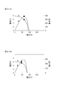
- 230000008859 change Effects 0.000 description 7
- 238000009499 grossing Methods 0.000 description 7
- 238000010248 power generation Methods 0.000 description 6
- 230000000694 effects Effects 0.000 description 5
- 230000009467 reduction Effects 0.000 description 5
- 230000007423 decrease Effects 0.000 description 4
- 230000000737 periodic effect Effects 0.000 description 4
- 238000005070 sampling Methods 0.000 description 4
- 235000019994 cava Nutrition 0.000 description 3
- 230000004069 differentiation Effects 0.000 description 3
- 238000004088 simulation Methods 0.000 description 3
- XEEYBQQBJWHFJM-UHFFFAOYSA-N Iron Chemical compound [Fe] XEEYBQQBJWHFJM-UHFFFAOYSA-N 0.000 description 2
- 238000004590 computer program Methods 0.000 description 2
- 230000008569 process Effects 0.000 description 2
- 230000002441 reversible effect Effects 0.000 description 2
- 230000001360 synchronised effect Effects 0.000 description 2
- NAWXUBYGYWOOIX-SFHVURJKSA-N (2s)-2-[[4-[2-(2,4-diaminoquinazolin-6-yl)ethyl]benzoyl]amino]-4-methylidenepentanedioic acid Chemical compound C1=CC2=NC(N)=NC(N)=C2C=C1CCC1=CC=C(C(=O)N[C@@H](CC(=C)C(O)=O)C(O)=O)C=C1 NAWXUBYGYWOOIX-SFHVURJKSA-N 0.000 description 1
- 230000003111 delayed effect Effects 0.000 description 1
- 230000005611 electricity Effects 0.000 description 1
- 230000005669 field effect Effects 0.000 description 1
- 230000006872 improvement Effects 0.000 description 1
- 229910052742 iron Inorganic materials 0.000 description 1
- 238000012986 modification Methods 0.000 description 1
- 230000004048 modification Effects 0.000 description 1
- 239000004065 semiconductor Substances 0.000 description 1
- 238000004904 shortening Methods 0.000 description 1
- 230000036962 time dependent Effects 0.000 description 1
Images


Classifications
-
- H—ELECTRICITY
- H02—GENERATION; CONVERSION OR DISTRIBUTION OF ELECTRIC POWER
- H02J—CIRCUIT ARRANGEMENTS OR SYSTEMS FOR SUPPLYING OR DISTRIBUTING ELECTRIC POWER; SYSTEMS FOR STORING ELECTRIC ENERGY
- H02J3/00—Circuit arrangements for ac mains or ac distribution networks
- H02J3/28—Arrangements for balancing of the load in a network by storage of energy
- H02J3/32—Arrangements for balancing of the load in a network by storage of energy using batteries with converting means
-
- H—ELECTRICITY
- H02—GENERATION; CONVERSION OR DISTRIBUTION OF ELECTRIC POWER
- H02J—CIRCUIT ARRANGEMENTS OR SYSTEMS FOR SUPPLYING OR DISTRIBUTING ELECTRIC POWER; SYSTEMS FOR STORING ELECTRIC ENERGY
- H02J3/00—Circuit arrangements for ac mains or ac distribution networks
- H02J3/38—Arrangements for parallely feeding a single network by two or more generators, converters or transformers
- H02J3/381—Dispersed generators
-
- H—ELECTRICITY
- H02—GENERATION; CONVERSION OR DISTRIBUTION OF ELECTRIC POWER
- H02J—CIRCUIT ARRANGEMENTS OR SYSTEMS FOR SUPPLYING OR DISTRIBUTING ELECTRIC POWER; SYSTEMS FOR STORING ELECTRIC ENERGY
- H02J7/00—Circuit arrangements for charging or depolarising batteries or for supplying loads from batteries
- H02J7/34—Parallel operation in networks using both storage and other dc sources, e.g. providing buffering
- H02J7/35—Parallel operation in networks using both storage and other dc sources, e.g. providing buffering with light sensitive cells
-
- H—ELECTRICITY
- H02—GENERATION; CONVERSION OR DISTRIBUTION OF ELECTRIC POWER
- H02M—APPARATUS FOR CONVERSION BETWEEN AC AND AC, BETWEEN AC AND DC, OR BETWEEN DC AND DC, AND FOR USE WITH MAINS OR SIMILAR POWER SUPPLY SYSTEMS; CONVERSION OF DC OR AC INPUT POWER INTO SURGE OUTPUT POWER; CONTROL OR REGULATION THEREOF
- H02M1/00—Details of apparatus for conversion
- H02M1/08—Circuits specially adapted for the generation of control voltages for semiconductor devices incorporated in static converters
-
- H—ELECTRICITY
- H02—GENERATION; CONVERSION OR DISTRIBUTION OF ELECTRIC POWER
- H02M—APPARATUS FOR CONVERSION BETWEEN AC AND AC, BETWEEN AC AND DC, OR BETWEEN DC AND DC, AND FOR USE WITH MAINS OR SIMILAR POWER SUPPLY SYSTEMS; CONVERSION OF DC OR AC INPUT POWER INTO SURGE OUTPUT POWER; CONTROL OR REGULATION THEREOF
- H02M1/00—Details of apparatus for conversion
- H02M1/44—Circuits or arrangements for compensating for electromagnetic interference in converters or inverters
-
- H—ELECTRICITY
- H02—GENERATION; CONVERSION OR DISTRIBUTION OF ELECTRIC POWER
- H02M—APPARATUS FOR CONVERSION BETWEEN AC AND AC, BETWEEN AC AND DC, OR BETWEEN DC AND DC, AND FOR USE WITH MAINS OR SIMILAR POWER SUPPLY SYSTEMS; CONVERSION OF DC OR AC INPUT POWER INTO SURGE OUTPUT POWER; CONTROL OR REGULATION THEREOF
- H02M3/00—Conversion of dc power input into dc power output
- H02M3/02—Conversion of dc power input into dc power output without intermediate conversion into ac
- H02M3/04—Conversion of dc power input into dc power output without intermediate conversion into ac by static converters
- H02M3/10—Conversion of dc power input into dc power output without intermediate conversion into ac by static converters using discharge tubes with control electrode or semiconductor devices with control electrode
- H02M3/145—Conversion of dc power input into dc power output without intermediate conversion into ac by static converters using discharge tubes with control electrode or semiconductor devices with control electrode using devices of a triode or transistor type requiring continuous application of a control signal
- H02M3/155—Conversion of dc power input into dc power output without intermediate conversion into ac by static converters using discharge tubes with control electrode or semiconductor devices with control electrode using devices of a triode or transistor type requiring continuous application of a control signal using semiconductor devices only
- H02M3/156—Conversion of dc power input into dc power output without intermediate conversion into ac by static converters using discharge tubes with control electrode or semiconductor devices with control electrode using devices of a triode or transistor type requiring continuous application of a control signal using semiconductor devices only with automatic control of output voltage or current, e.g. switching regulators
- H02M3/158—Conversion of dc power input into dc power output without intermediate conversion into ac by static converters using discharge tubes with control electrode or semiconductor devices with control electrode using devices of a triode or transistor type requiring continuous application of a control signal using semiconductor devices only with automatic control of output voltage or current, e.g. switching regulators including plural semiconductor devices as final control devices for a single load
- H02M3/1584—Conversion of dc power input into dc power output without intermediate conversion into ac by static converters using discharge tubes with control electrode or semiconductor devices with control electrode using devices of a triode or transistor type requiring continuous application of a control signal using semiconductor devices only with automatic control of output voltage or current, e.g. switching regulators including plural semiconductor devices as final control devices for a single load with a plurality of power processing stages connected in parallel
-
- H—ELECTRICITY
- H02—GENERATION; CONVERSION OR DISTRIBUTION OF ELECTRIC POWER
- H02M—APPARATUS FOR CONVERSION BETWEEN AC AND AC, BETWEEN AC AND DC, OR BETWEEN DC AND DC, AND FOR USE WITH MAINS OR SIMILAR POWER SUPPLY SYSTEMS; CONVERSION OF DC OR AC INPUT POWER INTO SURGE OUTPUT POWER; CONTROL OR REGULATION THEREOF
- H02M7/00—Conversion of ac power input into dc power output; Conversion of dc power input into ac power output
- H02M7/42—Conversion of dc power input into ac power output without possibility of reversal
- H02M7/44—Conversion of dc power input into ac power output without possibility of reversal by static converters
- H02M7/48—Conversion of dc power input into ac power output without possibility of reversal by static converters using discharge tubes with control electrode or semiconductor devices with control electrode
- H02M7/53—Conversion of dc power input into ac power output without possibility of reversal by static converters using discharge tubes with control electrode or semiconductor devices with control electrode using devices of a triode or transistor type requiring continuous application of a control signal
- H02M7/537—Conversion of dc power input into ac power output without possibility of reversal by static converters using discharge tubes with control electrode or semiconductor devices with control electrode using devices of a triode or transistor type requiring continuous application of a control signal using semiconductor devices only, e.g. single switched pulse inverters
- H02M7/5387—Conversion of dc power input into ac power output without possibility of reversal by static converters using discharge tubes with control electrode or semiconductor devices with control electrode using devices of a triode or transistor type requiring continuous application of a control signal using semiconductor devices only, e.g. single switched pulse inverters in a bridge configuration
- H02M7/53871—Conversion of dc power input into ac power output without possibility of reversal by static converters using discharge tubes with control electrode or semiconductor devices with control electrode using devices of a triode or transistor type requiring continuous application of a control signal using semiconductor devices only, e.g. single switched pulse inverters in a bridge configuration with automatic control of output voltage or current
-
- H—ELECTRICITY
- H02—GENERATION; CONVERSION OR DISTRIBUTION OF ELECTRIC POWER
- H02S—GENERATION OF ELECTRIC POWER BY CONVERSION OF INFRARED RADIATION, VISIBLE LIGHT OR ULTRAVIOLET LIGHT, e.g. USING PHOTOVOLTAIC [PV] MODULES
- H02S40/00—Components or accessories in combination with PV modules, not provided for in groups H02S10/00 - H02S30/00
- H02S40/30—Electrical components
- H02S40/32—Electrical components comprising DC/AC inverter means associated with the PV module itself, e.g. AC modules
-
- G—PHYSICS
- G05—CONTROLLING; REGULATING
- G05F—SYSTEMS FOR REGULATING ELECTRIC OR MAGNETIC VARIABLES
- G05F1/00—Automatic systems in which deviations of an electric quantity from one or more predetermined values are detected at the output of the system and fed back to a device within the system to restore the detected quantity to its predetermined value or values, i.e. retroactive systems
- G05F1/66—Regulating electric power
- G05F1/67—Regulating electric power to the maximum power available from a generator, e.g. from solar cell
-
- H—ELECTRICITY
- H02—GENERATION; CONVERSION OR DISTRIBUTION OF ELECTRIC POWER
- H02J—CIRCUIT ARRANGEMENTS OR SYSTEMS FOR SUPPLYING OR DISTRIBUTING ELECTRIC POWER; SYSTEMS FOR STORING ELECTRIC ENERGY
- H02J2300/00—Systems for supplying or distributing electric power characterised by decentralized, dispersed, or local generation
- H02J2300/20—The dispersed energy generation being of renewable origin
- H02J2300/22—The renewable source being solar energy
- H02J2300/24—The renewable source being solar energy of photovoltaic origin
- H02J2300/26—The renewable source being solar energy of photovoltaic origin involving maximum power point tracking control for photovoltaic sources
-
- H—ELECTRICITY
- H02—GENERATION; CONVERSION OR DISTRIBUTION OF ELECTRIC POWER
- H02J—CIRCUIT ARRANGEMENTS OR SYSTEMS FOR SUPPLYING OR DISTRIBUTING ELECTRIC POWER; SYSTEMS FOR STORING ELECTRIC ENERGY
- H02J3/00—Circuit arrangements for ac mains or ac distribution networks
- H02J3/38—Arrangements for parallely feeding a single network by two or more generators, converters or transformers
- H02J3/40—Synchronising a generator for connection to a network or to another generator
-
- H—ELECTRICITY
- H02—GENERATION; CONVERSION OR DISTRIBUTION OF ELECTRIC POWER
- H02M—APPARATUS FOR CONVERSION BETWEEN AC AND AC, BETWEEN AC AND DC, OR BETWEEN DC AND DC, AND FOR USE WITH MAINS OR SIMILAR POWER SUPPLY SYSTEMS; CONVERSION OF DC OR AC INPUT POWER INTO SURGE OUTPUT POWER; CONTROL OR REGULATION THEREOF
- H02M1/00—Details of apparatus for conversion
- H02M1/0048—Circuits or arrangements for reducing losses
-
- H—ELECTRICITY
- H02—GENERATION; CONVERSION OR DISTRIBUTION OF ELECTRIC POWER
- H02M—APPARATUS FOR CONVERSION BETWEEN AC AND AC, BETWEEN AC AND DC, OR BETWEEN DC AND DC, AND FOR USE WITH MAINS OR SIMILAR POWER SUPPLY SYSTEMS; CONVERSION OF DC OR AC INPUT POWER INTO SURGE OUTPUT POWER; CONTROL OR REGULATION THEREOF
- H02M1/00—Details of apparatus for conversion
- H02M1/0067—Converter structures employing plural converter units, other than for parallel operation of the units on a single load
- H02M1/007—Plural converter units in cascade
-
- H—ELECTRICITY
- H02—GENERATION; CONVERSION OR DISTRIBUTION OF ELECTRIC POWER
- H02M—APPARATUS FOR CONVERSION BETWEEN AC AND AC, BETWEEN AC AND DC, OR BETWEEN DC AND DC, AND FOR USE WITH MAINS OR SIMILAR POWER SUPPLY SYSTEMS; CONVERSION OF DC OR AC INPUT POWER INTO SURGE OUTPUT POWER; CONTROL OR REGULATION THEREOF
- H02M7/00—Conversion of ac power input into dc power output; Conversion of dc power input into ac power output
- H02M7/42—Conversion of dc power input into ac power output without possibility of reversal
- H02M7/44—Conversion of dc power input into ac power output without possibility of reversal by static converters
- H02M7/48—Conversion of dc power input into ac power output without possibility of reversal by static converters using discharge tubes with control electrode or semiconductor devices with control electrode
- H02M7/4826—Conversion of dc power input into ac power output without possibility of reversal by static converters using discharge tubes with control electrode or semiconductor devices with control electrode operating from a resonant DC source, i.e. the DC input voltage varies periodically, e.g. resonant DC-link inverters
-
- Y—GENERAL TAGGING OF NEW TECHNOLOGICAL DEVELOPMENTS; GENERAL TAGGING OF CROSS-SECTIONAL TECHNOLOGIES SPANNING OVER SEVERAL SECTIONS OF THE IPC; TECHNICAL SUBJECTS COVERED BY FORMER USPC CROSS-REFERENCE ART COLLECTIONS [XRACs] AND DIGESTS
- Y02—TECHNOLOGIES OR APPLICATIONS FOR MITIGATION OR ADAPTATION AGAINST CLIMATE CHANGE
- Y02B—CLIMATE CHANGE MITIGATION TECHNOLOGIES RELATED TO BUILDINGS, e.g. HOUSING, HOUSE APPLIANCES OR RELATED END-USER APPLICATIONS
- Y02B70/00—Technologies for an efficient end-user side electric power management and consumption
- Y02B70/10—Technologies improving the efficiency by using switched-mode power supplies [SMPS], i.e. efficient power electronics conversion e.g. power factor correction or reduction of losses in power supplies or efficient standby modes
-
- Y—GENERAL TAGGING OF NEW TECHNOLOGICAL DEVELOPMENTS; GENERAL TAGGING OF CROSS-SECTIONAL TECHNOLOGIES SPANNING OVER SEVERAL SECTIONS OF THE IPC; TECHNICAL SUBJECTS COVERED BY FORMER USPC CROSS-REFERENCE ART COLLECTIONS [XRACs] AND DIGESTS
- Y02—TECHNOLOGIES OR APPLICATIONS FOR MITIGATION OR ADAPTATION AGAINST CLIMATE CHANGE
- Y02E—REDUCTION OF GREENHOUSE GAS [GHG] EMISSIONS, RELATED TO ENERGY GENERATION, TRANSMISSION OR DISTRIBUTION
- Y02E10/00—Energy generation through renewable energy sources
- Y02E10/50—Photovoltaic [PV] energy
- Y02E10/56—Power conversion systems, e.g. maximum power point trackers
Definitions
- the present invention relates to a power conversion device and a control method thereof.
- This application claims priority based on Japanese Application No. 2015-199521 filed on Oct. 7, 2015, and incorporates all the description items described in the above Japanese application.
- a power conversion device used as a power conditioner for solar power generation converts a direct-current generated power into an alternating current and performs an operation linked to the commercial power system.
- the generated voltage is boosted by a booster circuit to a constant voltage higher than the peak voltage on the AC side, and then converted into an AC voltage by an inverter circuit.
- the booster circuit and the inverter circuit always perform a high-speed switching operation.
- the present invention is a power conversion device that is provided between an AC system and a DC power source that outputs a voltage lower than the peak value of the absolute value of the AC voltage in the AC system, and performs DC / AC power conversion,
- a filter circuit connected to the AC system, a DC / DC converter provided between the DC power supply and a DC bus, a capacitor connected to the DC bus, the DC bus, and the filter circuit.
- a DC / AC converter provided therebetween, and a controller for controlling the DC / DC converter and the DC / AC converter,
- the control unit obtains an output current target value based on an input power value of DC power and a voltage value of the AC system, and calculates a current target value and a voltage target value of the DC / AC converter based on the output current target value.
- the control unit controls the output of AC power by obtaining the target value and controlling the DC / DC converter, and the control unit sets the DC voltage value of the DC power source as the voltage target value of the DC / DC converter, the DC /
- the absolute value of the voltage target value on the AC side of the AC converter and the DC voltage lower limit value that is a predetermined value smaller than the peak value of the absolute value are the largest at that time Selecting have value, a power conversion apparatus.
- the present invention also provides a filter circuit provided between an AC system and a DC power source that outputs a voltage lower than the peak value of the absolute value of the AC voltage in the AC system, and connected to the AC system, and the DC A DC / DC converter provided between a power supply and a DC bus; a capacitor connected to the DC bus; a DC / AC converter provided between the DC bus and the filter circuit; A control method executed by a power conversion device that performs DC / AC power conversion, As a basic control method, an output current target value is obtained based on an input power value of DC power and a voltage value of the AC system, and a current target value and a voltage target value of the DC / AC converter are calculated based on the output current target value.
- the DC / AC converter circuit is controlled, and the current target value and voltage target value of the DC / AC converter and the current target value of the DC / DC converter are determined based on the voltage target value of the DC / DC converter.
- the control unit includes, as the voltage target value of the DC / DC converter, a DC voltage value of the DC power supply, an absolute value of a voltage target value on the AC side of the DC / AC converter, and the absolute value
- the largest value at that time is selected from the DC voltage lower limit value that is a predetermined value smaller than the peak value.
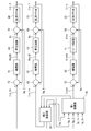
- FIG. 1 It is a block diagram which shows an example of the system provided with the inverter apparatus which concerns on one Embodiment. It is an example of the circuit diagram of an inverter apparatus. It is a block diagram of a control part.
- First DC input voltage detection value Vg.1 (vertical axis is [V])
- first booster circuit current detection value Iin.1 (vertical axis is [A])
- first DC input current detection value Ig.1 (A vertical axis is [A])
- FIG. 9A is a schematic diagram showing how to obtain the booster circuit voltage target value Vo *
- FIG. 9A is a diagram showing a comparison between the inverter output voltage target value Vinv * and the first DC input voltage detection value Vg.1.
- 9B is a diagram illustrating a waveform of the booster circuit voltage target value Vo *, and FIG.
- 9C is a diagram illustrating a case where the power output from the second booster circuit is boosted with reference to the second DC input voltage detection value Vg.2. is there.
- the graph showing the results of the time-dependent changes of the DC input voltage detection values Vg.1, Vg.2 and the booster circuit voltage target value Vo * together with the target values.
- the upper graph shows the inverter output voltage.
- the middle graph is the graph showing the relationship between the DC input voltage values Vg.1, Vg.2 and the booster circuit voltage target value Vo *.
- the lower graph is a graph showing the boost circuit current target values Iin.1 * and Iin.2 * (the vertical axis of voltage is [V] and the vertical axis of current is [A]).
- (A) is a graph comparing the first booster circuit carrier wave with the waveform of the first booster circuit voltage reference value Vbc1 #, and (b) driving the switching element generated by the first booster circuit controller. It is a drive waveform for doing.
- (A) is a graph comparing the inverter circuit carrier and the waveform of the inverter voltage reference value Vinv #
- (b) is a drive waveform for driving the switching element Q1 generated by the inverter circuit control unit
- (c) ) Is a drive waveform for driving the switching element Q3 generated by the inverter circuit control unit. It is the figure which showed an example of the drive wave of a reference wave and each switching element (The vertical axis
- (A) is a graph comparing the second booster circuit carrier and the waveform of the second booster circuit voltage reference value Vbc2 # (the vertical axis is [V]), and (b) is the second booster circuit controller. It is a drive waveform for driving the generated switching element.
- (A) is the graph which showed each voltage waveform of the alternating voltage output from the inverter circuit, the commercial power system, and the both-ends voltage of an AC reactor, (b) showed the current waveform which flows into an AC reactor. It is a graph. It is a block diagram which shows an example of the system by which the power converter device was provided between two types of DC power supplies and an AC system. It is an example of the circuit diagram of the power converter device in FIG.
- FIG. 25A shows the voltage target value Vo * (solid line), the reactive current Ico (dashed line) and the reactive power (Ico ⁇ Vo *) (dashed line) when the voltage target value Vo * of FIG. 24 is adopted.
- FIG. 25A shows the voltage target value Vo * (solid line), the reactive current Ico (dashed line) and the reactive power (Ico ⁇ Vo *) (dashed line) when the voltage target value Vo * of FIG. 24 is adopted.
- FIG. 25B is a waveform diagram showing current (Ico ⁇ Vo * / n / Vg.i).
- FIG. 26A and FIG. 26B are diagrams showing the characteristics of MPPT control by the DC / DC converter when a lower limit value is not given to Vo * for comparison.
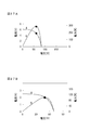
- 27A and 27B are diagrams illustrating characteristics of MPPT control by the DC / DC converter when the voltage lower limit value Vo_limit is given to Vo *.
- the voltage input to the power converter has a wide range, and a DC voltage that is considerably lower than the effective value of the AC voltage may be input.
- a large reactive power is generated by the smoothing capacitor connected to the DC bus connecting the booster circuit and the inverter circuit, which increases the control accuracy. It has been found to have some effect.
- the present disclosure basically reduces the control accuracy even when a DC voltage that is considerably lower than the effective value of the AC voltage is input in a power conversion device that performs control having a switching operation pause period. It aims at suppressing.
- the gist of the embodiment of the present invention includes at least the following.
- This is a power conversion device that is provided between an AC system and a DC power source that outputs a voltage lower than the peak value of the absolute value of the AC voltage in the AC system, and performs DC / AC power conversion.
- a filter circuit connected to the AC system, a DC / DC converter provided between the DC power supply and a DC bus, a capacitor connected to the DC bus, the DC bus, and the filter circuit.
- a DC / AC converter provided therebetween, and a controller for controlling the DC / DC converter and the DC / AC converter, The control unit obtains an output current target value based on an input power value of DC power and a voltage value of the AC system, and calculates a current target value and a voltage target value of the DC / AC converter based on the output current target value.
- the control unit controlling the DC / AC converter circuit, and based on the current target value and voltage target value of the DC / AC converter, and the voltage target value of the DC / DC converter, the current of the DC / DC converter
- the control unit As the voltage target value of the DC / DC converter, is smaller than the DC voltage value of the DC power supply, the absolute value of the voltage target value on the AC side of the DC / AC converter, and the peak value of the absolute value. It is a power converter which selects the largest value at the time among the DC voltage lower limit which is a predetermined value.
- the absolute value of the DC voltage value of the DC power supply and the voltage target value on the AC side of the DC / AC converter The larger one is the voltage target value of the DC / DC converter at that time. In this case, both the DC / DC converter and the DC / AC converter have a pause in switching within the AC cycle.
- the larger one of the DC voltage lower limit value and the absolute value of the voltage target value on the AC side of the DC / AC converter is the DC current value at that time. This is the voltage target value of the DC converter.
- the voltage target value of the DC / DC converter has a waveform that takes the larger one of the DC voltage lower limit value and the absolute value of the voltage target value on the AC side of the DC / AC converter.
- the DC / DC converter is not paused and is boosted to the DC voltage lower limit value.
- condenser connected to DC bus can be suppressed.
- the effective current control that is originally desired can be performed with higher accuracy. Therefore, in a power conversion device that basically performs control with a switching operation pause period, it is possible to suppress a reduction in control accuracy even when a DC voltage that is considerably lower than the effective value of the AC voltage is input.
- the power conversion device of (1) for example, a plurality of sets of the DC power supply and the DC / DC converter are provided, and there are a plurality of DC voltage values of the DC power supply, and a plurality of DC voltages exist.
- the maximum value among the values is a target to be compared with the DC voltage lower limit value.
- the reactive power of each DC / DC converter can be reduced by sharing the reactive power with a plurality of DC / DC converters.
- the DC voltage lower limit value shortens the period during which reactive power is generated and increases the period during which reactive power is zero. Selected. In this case, even if the reactive power peak value cannot be suppressed, the reactive power can be suppressed in the zero period, so that the active power can be controlled more easily.
- the DC voltage lower limit value is selected so that the period during which reactive power is generated is less than half of the AC (1/2) cycle. In this case, since the period during which the reactive power is 0 can be ensured by more than half of the AC (1/2) cycle, the effect of suppressing the reactive power is likely to occur.
- a filter provided between the AC system and a DC power source that outputs a voltage lower than the peak value of the absolute value of the AC voltage in the AC system and connected to the AC system.
- a circuit a DC / DC converter provided between the DC power source and the DC bus, a capacitor connected to the DC bus, a DC / AC provided between the DC bus and the filter circuit.
- a control method executed by a power conversion device that has a converter and performs DC / AC power conversion As a basic control method, an output current target value is obtained based on an input power value of DC power and a voltage value of the AC system, and a current target value and a voltage target value of the DC / AC converter are calculated based on the output current target value. And the DC / AC converter circuit is controlled, and the current target value and voltage target value of the DC / AC converter and the current target value of the DC / DC converter are determined based on the voltage target value of the DC / DC converter.
- the control unit By controlling the DC / DC converter by obtaining a value, the output of AC power is controlled,
- the control unit includes, as the voltage target value of the DC / DC converter, a DC voltage value of the DC power supply, an absolute value of a voltage target value on the AC side of the DC / AC converter, and the absolute value
- the largest value at that time is selected from the DC voltage lower limit value that is a predetermined value smaller than the peak value.
- the voltage target value of the DC / DC converter has a waveform that takes the larger one of the DC voltage lower limit value and the absolute value of the voltage target value on the AC side of the DC / AC converter.
- the DC / DC converter is not paused and is boosted to the DC voltage lower limit value.
- condenser connected to DC bus can be suppressed.
- the effective current control that is originally desired can be performed with higher accuracy. Therefore, in a power conversion device that basically performs control with a switching operation pause period, it is possible to suppress a reduction in control accuracy even when a DC voltage that is considerably lower than the effective value of the AC voltage is input.
- a power converter device can also be expressed as follows separately from the expressions (1) and (4).
- a power conversion device that is provided between an AC system and a DC power source that outputs a voltage lower than the peak value of the absolute value of the AC voltage in the AC system, and performs DC / AC power conversion.
- a DC / DC converter Provided between the connected filter circuit, a DC / DC converter provided between the DC power source and the DC bus, a capacitor connected to the DC bus, the DC bus, and the filter circuit.
- a DC / AC converter and a controller for controlling the DC / DC converter and the DC / AC converter,
- the control unit obtains an output current target value based on an input power value of DC power and a voltage value of the AC system, and calculates a current target value and a voltage target value of the DC / AC converter based on the output current target value.
- the control unit controlling the DC / AC converter circuit, and based on the current target value and voltage target value of the DC / AC converter, and the voltage target value of the DC / DC converter, the current of the DC / DC converter
- the control unit By controlling the DC / DC converter by obtaining a target value, the output of AC power is controlled,
- the control unit as the voltage target value of the DC / DC converter, is smaller than the DC voltage value of the DC power supply, the absolute value of the voltage target value on the AC side of the DC / AC converter, and the peak value of the absolute value.
- a power conversion device that selects a maximum value of DC voltage lower limit values that are predetermined values at that time and makes a period during which a part of the pulsating waveform of the absolute value appears is less than half of one cycle of pulsating flow It is.
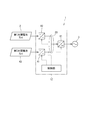
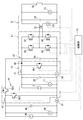
- FIG. 1 is a block diagram illustrating an example of a system including an inverter device according to an embodiment.
- the first solar cell array 2 and the second solar cell array 40 as DC power sources are connected to the input terminal of the inverter device 1, and the AC commercial power system 3 is connected to the output terminal.
- This system converts DC power generated by the first solar cell array 2 (hereinafter also simply referred to as the first array 2) and the second solar cell array 40 (hereinafter also simply referred to as the second array 40) into AC power. Then, an interconnection operation for outputting to the commercial power system 3 is performed.
- the first array 2 and the second array 40 are configured by connecting a plurality of photovoltaic power generation panels (modules) in series and parallel.
- the second array 40 is configured such that the power voltage output from the second array 40 is smaller than the power voltage output from the first array 2.
- the inverter device 1 includes a first booster circuit 10 to which DC power output from the first array 2 is applied, a second booster circuit 41 to which DC power output from the second array 40 is applied, and both booster circuits 10 and 41.
- An inverter circuit 11 that converts electric power output to the DC bus 20 into AC power and outputs it to the commercial power system 3, and a control unit 12 that controls operations of these circuits 10, 11, 42 are provided.
- the first booster circuit 10 and the second booster circuit 41 are connected in parallel to the inverter circuit 11.
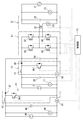
- FIG. 2 is an example of a circuit diagram of the inverter device 1.
- the first booster circuit 10 to which the first array 2 is connected includes a DC reactor 15, a diode 16, and a switching element Qb1 made of an IGBT (Insulated Gate Bipolar Transistor) or the like, and constitutes a boost chopper circuit. ing.
- the diode 16 may be replaced with a switching element.
- a first voltage sensor 17, a first current sensor 18, and a smoothing capacitor 26 are provided on the input side of the first booster circuit 10.
- the first voltage sensor 17 detects the first DC input voltage detection value Vg.1 (DC input voltage value) of the DC power output from the first array 2 and input to the first booster circuit 10, and the control unit 12. Output to.
- the first current sensor 18 detects a first booster circuit current detection value Iin.1 that is a current flowing through the DC reactor 15, and outputs it to the control unit 12.
- the second booster circuit 41 to which the second array 40 is connected includes a DC reactor 42, a diode 43, and a switching element Qb2 made of IGBT or the like, and constitutes a boost chopper circuit like the first booster circuit. is doing.
- the diode 43 may be replaced with a switching element.
- a second voltage sensor 44, a second current sensor 45, and a smoothing capacitor 46 are provided on the input side of the second booster circuit 41.
- the second voltage sensor 44 outputs a second DC input voltage detection value Vg. Of DC power output from the second array 40 and input to the second booster circuit 41. 2 is detected and output to the control unit 12.
- the second current sensor 45 detects the second booster circuit current detection value Iin.2, which is a current flowing through the DC reactor 42, and outputs it to the control unit 12.
- the control unit 12 calculates input powers Pin.1 and Pin.2 from the DC input voltage detection values Vg.1, Vg.2 and the booster circuit current detection values Iin.1, Iin.2, and the first array 2 and the first array 2 It has a function to perform MPPT (Maximum Power Point Tracking) control for the two arrays 40.
- MPPT Maximum Power Point Tracking
- the switching element Qb1 of the first booster circuit 10 is controlled by the control unit 12 so that the period for performing the switching operation with the inverter circuit 11 is alternately switched as described later. Therefore, the first booster circuit 10 outputs the boosted power to the inverter circuit 11 during the period when the switching operation is performed, and the first array 2 outputs the first power during the period when the switching operation is stopped. The DC power input to the booster circuit 10 is output to the inverter circuit 11 without being boosted.
- the second booster circuit 41 converts the voltage value of the DC power supplied from the second array 40 into the first DC input that is the voltage value of the DC power supplied from the first array 2 during a predetermined period. Control is performed by the control unit 12 so that the voltage is boosted to a value substantially equal to the detected voltage value Vg.1 and output.
- a smoothing capacitor 19 is connected between the booster circuits 10 and 41 and the inverter circuit 11.
- the inverter circuit 11 includes switching elements Q1 to Q4 made of FET (Field Effect Transistor). These switching elements Q1 to Q4 constitute a full bridge circuit. Each of the switching elements Q1 to Q4 is connected to the control unit 12, and can be controlled by the control unit 12.
- the control unit 12 performs PWM control of the operations of the switching elements Q1 to Q4. Thereby, the inverter circuit 11 converts the electric power given from both the booster circuits 10 and 41 into alternating current power.
- the inverter device 1 includes a filter circuit 21 between the inverter circuit 11 and the commercial power system 3.
- the filter circuit 21 includes two AC reactors 22 and a capacitor 23.
- the filter circuit 21 has a function of removing high-frequency components contained in the AC power output from the inverter circuit 11. The AC power from which the high frequency component has been removed by the filter circuit 21 is supplied to the commercial power system 3.
- the filter circuit 21 is connected to a third current sensor 24 for detecting an inverter current detection value Iinv (current flowing through the AC reactor 22), which is a current value output from the inverter circuit 11. Further, a third voltage sensor 25 for detecting a voltage value (system voltage detection value Va) on the commercial power system 3 side is connected between the filter circuit 21 and the commercial power system 3.
- the third current sensor 24 and the third voltage sensor 25 output the detected inverter current detection value Iinv and the system voltage detection value Va to the control unit 12. Based on the system voltage detection value Va and the inverter current detection value Iinv, the DC input voltage detection values Vg.1, Vg.2, and the booster circuit current detection values Iin.1, Iin. Both booster circuits 10 and 41 and the inverter circuit 11 are controlled.
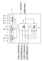
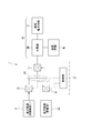
- FIG. 3 is a block diagram of the control unit 12.
- the control unit 12 includes a control processing unit 30, a first boost circuit control unit 32, an inverter circuit control unit 33, an averaging processing unit 34, and a second boost circuit control unit 35.
- a part or all of the functions of the control unit 12 may be configured by a hardware circuit, or part or all of the functions may be realized by causing a computer (computer program) to be executed by a computer. .
- Software (computer program) for realizing the function of the control unit 12 is stored in a storage device (not shown) of the computer.
- the first booster circuit control unit 32 controls the switching element Qb1 of the first booster circuit 10 based on the target value and the detection value given from the control processing unit 30, and the power of the current corresponding to the target value is the first.
- the voltage is output to the booster circuit 10.
- the second booster circuit control unit 35 controls the switching element Qb2 of the second booster circuit 41 based on the target value and the detection value given from the control processing unit 30, and the second power is supplied to the current corresponding to the target value.
- the voltage is output to the booster circuit 41.
- the inverter circuit control unit 33 controls the switching elements Q1 to Q4 of the inverter circuit 11 based on the target value and the detection value given from the control processing unit 30, and the electric power of the current corresponding to the target value is converted to the inverter circuit. 11 to output.
- the control processing unit 30 is provided with DC input voltage detection values Vg.1, Vg.2, booster circuit current detection values Iin.1, Iin.2, system voltage detection value Va, and inverter current detection value Iinv.
- the control processing unit 30 calculates the first input power Pin.1 and the average value of the first booster circuit 10 from the DC input voltage detection values Vg.1, Vg.2 and the booster circuit current detection values Iin.1, Iin.2.
- ⁇ Pin.1>, the second input power Pin.2 of the second booster circuit 41, and its average value ⁇ Pin.2> are calculated.
- the control processing unit 30 sets a first DC input current target value Ig.1 * (described later) of the first booster circuit 10 based on the first input power average value ⁇ Pin.1>, and the first array 2 has a function of performing MPPT control and feedback control of each of the first booster circuit 10 and the inverter circuit 11. Further, the control processing unit 30 sets a DC input current target value Ig.2 * (described later) of the second booster circuit 41 based on the second input power average value ⁇ Pin.2>, and the second array MPPT control is performed for 40, and the second booster circuit 41 is also feedback controlled.
- the DC input voltage detection values Vg.1, Vg.2 and the booster circuit current detection values Iin.1, Iin.2 are given to the averaging processing unit 34 and the control processing unit 30.
- the averaging processing unit 34 obtains the DC input voltage detection values Vg.1, Vg.2 and the booster circuit current detection values Iin.1, Iin.2 given from the voltage sensors 17, 44 and the current sensors 18, 45, Sampling is performed at predetermined time intervals set in advance, and the respective average values are obtained, and the averaged DC input voltage detection values Vg.1, Vg.2 and booster circuit current detection values Iin.1, Iin.2 are obtained. It has a function to be given to the control processing unit 30.
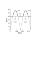
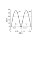
- FIG. 4 is a graph showing an example of results obtained by simulating changes with time of the first DC input voltage detection value Vg.1 and the first booster circuit current detection value Iin.1.
- the first booster circuit current detection value Iin.1 appears as a waveform synchronized with the system voltage based on the target value, as will be described later. Further, the first DC input current detection value Ig.1 is a current value detected on the input side from the capacitor 26.
- the first DC input voltage detection value Vg.1 and the first DC input current detection value Ig.1 are half of the system voltage. It turns out that it fluctuates with a period.
- the reason why the first DC input voltage detection value Vg.1 and the first DC input current detection value Ig.1 periodically change is as follows. That is, the first booster circuit current detection value Iin.1 of the inverter device 1 greatly fluctuates from approximately 0 A to a peak value in a half cycle of the AC cycle according to the operations of the booster circuit 10 and the inverter circuit 11. Therefore, the fluctuation component cannot be completely removed by the capacitor 26, and the first DC input current detection value Ig.1 becomes a pulsating flow including a component that fluctuates in a half cycle of the AC cycle. On the other hand, the output voltage of the photovoltaic power generation panel changes depending on the output current. Therefore, the periodic fluctuation occurring in the first DC input voltage detection value Vg.1 is a half cycle of the AC power output from the inverter device 1. That is, it is a half cycle of the commercial power system 3.
- the averaging processing unit 34 averages the first DC input voltage detection value Vg.1 and the first booster circuit current detection value Iin.1 in order to suppress the influence due to the above-described periodic fluctuation.
- FIG. 5 is a diagram illustrating an aspect when the first DC input voltage detection value Vg.1 is averaged by the averaging processing unit 34.
- the averaging processing unit 34 samples the given first DC input voltage detection value Vg.1 a plurality of times at a predetermined time interval ⁇ t in a period L from a certain timing t1 to a timing t2. (A black dot timing in the figure) is performed, and an average value of the obtained first DC input voltage detection values Vg.1 is obtained.
- the averaging processing unit 34 sets the period L to a length that is 1 ⁇ 2 of the periodic length of the commercial power system 3.
- the averaging processing unit 34 sets the time interval ⁇ t to a period sufficiently shorter than the length of the 1 ⁇ 2 cycle of the commercial power system 3.
- the averaging processing unit 34 reduces the average value of the first DC input voltage detection value Vg.1 that periodically fluctuates in 1/2 cycle of the commercial power system 3 while shortening the sampling period as much as possible. It can be obtained with high accuracy.
- the sampling time interval ⁇ t can be set to, for example, 1/100 to 1/1000 of the cycle of the commercial power system 3, 20 microseconds to 200 microseconds, or the like.
- the averaging processing unit 34 may store the period L in advance, or may acquire information on the cycle of the commercial power system 3 by acquiring the system voltage detection value Va from the third voltage sensor 25. it can.
- the period L is set to 1 ⁇ 2 of the cycle length of the commercial power system 3, but if the period L is set to at least 1 ⁇ 2 period of the commercial power system 3, the first period is set.
- the average value of the DC input voltage detection value Vg.1 can be obtained with high accuracy.
- the first DC input voltage detection value Vg.1 periodically fluctuates with a length of 1 ⁇ 2 of the periodic length of the commercial power system 3 by the operations of the booster circuit 10 and the inverter circuit 11. Because.
- the period L is set to an integral multiple of the 1/2 cycle of the commercial power system 3, such as 3 or 4 times the 1/2 cycle of the commercial power system 3. do it.
- the voltage fluctuation can be grasped in units of cycles.
- the first booster circuit current detection value Iin.1 also periodically fluctuates in a half cycle of the commercial power system 3, as with the first DC input voltage detection value Vg.1. Therefore, the averaging processing unit 34 also obtains the average value of the first booster circuit current detection value Iin.1 by the same method as the first DC input voltage detection value Vg.1 shown in FIG.
- the second DC input voltage detection value Vg.2 and the second booster circuit current detection value Iin.2 on the second array 40 side are also the same as the first DC input voltage detection value Vg.1. It fluctuates periodically in 1/2 cycle of the commercial power system 3. Therefore, the averaging processing unit 34 performs the second DC input voltage detection value Vg.2 and the second booster circuit current detection value Iin by the same method as the first DC input voltage detection value Vg.1 shown in FIG. .2 Find the average of each.
- the control processing unit 30 sequentially obtains the average value of the DC input voltage detection values Vg.1, Vg.2 and the average value of the boost circuit current detection values Iin.1, Iin.2 for each period L.
- the averaging processing unit 34 gives the average value of the obtained DC input voltage detection values Vg.1, Vg.2 and the average value of the boost circuit current detection values Iin.1, Iin.2 to the control processing unit 30.
- the averaging processing unit 34 performs the DC input voltage detection value Vg. 1, Vg. 2 and the boost circuit current detection values Iin1 and Iin2 are obtained, and the control processing unit 30 uses these values to perform MPPT control on both arrays 2 and 40, while both boosting circuits 10 and 41 and Since the inverter circuit 11 is controlled, even when the DC currents of both arrays 2 and 40 fluctuate and become unstable, the control unit 12 outputs the outputs from both arrays 2 and 40 to the DC input voltage detection value Vg. 1, Vg. 2 and the average value of the boost circuit current detection values Iin1 and Iin2 can be obtained with high accuracy. As a result, MPPT control can be performed suitably and it can suppress effectively that power supply efficiency falls.
- the DC power voltage (DC input voltage detection values Vg.1, Vg.2) and current (booster circuit current detection) output from both arrays 2 and 40 due to fluctuations in the input current of the inverter device 1 are described.
- the fluctuation period coincides with a half period of AC power output from the inverter circuit 11 (a half period of the commercial power system 3).
- the DC input voltage detection values Vg.1, Vg.2 and the boost circuit current detection are detected during the period L set to 1 ⁇ 2 of the cycle length of the commercial power system 3.
- Each of the values Iin.1 and Iin.2 is sampled a plurality of times at a time interval ⁇ t sufficiently shorter than a half cycle of the AC system, and the average of the DC input voltage detection values Vg.1 and Vg.2 is obtained from the result.
- Value and the average value of the boost circuit current detection values Iin.1 and Iin.2 even if the voltage and current of the DC current fluctuate periodically, the DC input voltage detection values Vg.1, Vg.2 and The boost circuit current detection values Iin.1 and Iin.2 can be obtained with high accuracy.
- the DC input voltage detection values Vg.1, Vg.2 and the booster circuit current detection values Iin.1, Iin.2 given from both arrays 2 and 40 are as described above for the inverter circuit 11 and the like. This is due to fluctuations in impedance. Therefore, the DC input voltage detection values Vg.1, Vg.2 and the booster circuit current detection values Iin.1, Iin.2 are plural at a time interval ⁇ t shorter than a half cycle of the AC power output from the inverter circuit 11. It may be a value obtained from the result of sampling twice.
- the control processing unit 30 sets the DC input current target values Ig.1 * and Ig.2 * based on the above-described average input power values ⁇ Pin.1> and ⁇ Pin.2>. Based on the current target values Ig.1 * and Ig.2 * and the above values, the target values for the booster circuits 10 and 41 and the inverter circuit 11 are obtained.
- the control processing unit 30 gives the obtained target value to the first booster circuit control unit 32, the second booster circuit control unit 35, and the inverter circuit control unit 33, and feedback controls each of the booster circuits 10, 41 and the inverter circuit 11. It has a function to do.
- FIG. 6 is a control block diagram for explaining the control processing by the control processing unit 30.
- the control processing unit 30 includes a first calculation unit 51, a first adder 52, a compensator 53, and a second adder 54 as functional units for controlling the inverter circuit 11. Further, the control processing unit 30 functions as a functional unit for controlling both the booster circuits 10 and 41.
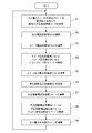
- FIG. 7 is a flowchart showing the control processing of both the booster circuits 10 and 41 and the inverter circuit 11.
- Each functional unit shown in FIG. 6 controls both booster circuits 10 and 41 and the inverter circuit 11 by executing the processing shown in the flowchart shown in FIG.
- the control processing of both booster circuits 10 and 41 and the inverter circuit 11 will be described with reference to FIG.
- the control processing unit 30 obtains the current input power average value ⁇ Pin.i> (step S9), and compares it with the input power average value ⁇ Pin.i> at the previous calculation to determine the DC input current target value Ig. i * is set (step S1).
- the input power average value ⁇ Pin.i> is obtained based on the following formula (1).
- Input power average value ⁇ Pin.i> ⁇ Iin.i ⁇ Vg.i> ... (1)
- ⁇ Pin.1> indicates the average input power value in the first booster circuit 10
- ⁇ Pin.2> indicates the average input power value in the second booster circuit 41.
- the control processing unit 30 obtains the input power average values ⁇ Pin.1> and ⁇ Pin.2>, and sets the DC input current target values Ig.1 * and Ig.2 *.
- Iin.i is a boost circuit current detection value
- Vg.i is a DC input voltage detection value
- these boost circuit current detection value Iin.i and DC input voltage detection value Vg.i are The value averaged by the averaging processing unit 34.
- instantaneous values that are not averaged are used for the boost circuit current detection value Iin.i and the DC input voltage detection value Vg.i. That is, the average value of the boost circuit current detection value Iin.i and the average value of the DC input voltage detection value Vg.i are used to obtain the input power average value ⁇ Pin.i>.
- “ ⁇ >” indicates an average value or an effective value of values in parentheses. The same applies hereinafter.
- the control processing unit 30 gives the set DC input current target value Ig.i * to the first calculation unit 51.
- the first calculation unit 51 is also provided with a DC input voltage detection value Vg.i and a system voltage detection value Va.
- the first calculation unit 51 uses the given DC input current target value Ig.i *, DC input voltage detection value Vg.i, and system voltage detection value Va, based on the following formula (2), to inverter device 1
- the effective value ⁇ Ia *> of the output current target value is calculated.
- the first calculation unit 51 obtains the output current target value Ia * based on the following formula (3) (step S2).
- the first calculation unit 51 obtains the output current target value Ia * as a sine wave having the same phase as the system voltage detection value Va.
- Output current target value Ia * (2 1/2 ) ⁇ ⁇ Ia *> ⁇ sin ⁇ t ... (3)
- the first calculation unit 51 calculates an inverter current target value Iinv *, which is a current target value for controlling the inverter circuit 11, as shown in the following formula (4) (step S3).
- Inverter current target value Iinv * Ia * + s CaVa ... (4)
- the first calculation unit 51 When the first calculation unit 51 obtains the inverter current target value Iinv *, it supplies the inverter current target value Iinv * to the first adder 52.
- the inverter circuit 11 is feedback-controlled by this inverter current target value Iinv *.
- the current adder current detection value Iinv is given to the first adder 52.
- the first adder 52 calculates the difference between the inverter current target value Iinv * and the current inverter current detection value Iinv, and gives the calculation result to the compensator 53.
- the compensator 53 converges the difference based on a proportional coefficient or the like to obtain an inverter voltage reference value Vinv # that can be used as the inverter current detection value Iinv * as the inverter current target value Iinv *.
- the compensator 53 gives this inverter voltage reference value Vinv # to the inverter circuit control unit 33, thereby causing the inverter circuit 11 to output power according to the inverter output voltage target value Vinv *.
- the electric power output from the inverter circuit 11 is subtracted by the system voltage detection value Va by the second adder 54, is then supplied to the AC reactor 22, and is fed back as a new inverter current detection value Iinv.
- the difference between the inverter current target value Iinv * and the inverter current detection value Iinv is calculated again by the first adder 52, and the inverter circuit 11 is controlled based on this difference as described above.
- the inverter circuit 11 is feedback-controlled by the inverter current target value Iinv * and the inverter current detection value Iinv (step S4).
- the second calculation unit 61 is provided with the inverter current target value Iinv * calculated by the first calculation unit 51 in addition to the DC input voltage detection value Vg.i and the system voltage detection value Va.
- the second calculator 61 calculates the inverter output voltage target value Vinv * based on the following equation (5) (step S5).
- Inverter output voltage target value Vinv * Va + s LaIinv * (5)
- the second term on the right side is a value added in consideration of the voltage generated at both ends of the AC reactor 22.
- the inverter current target value Iinv * that is a current target value for controlling the inverter circuit 11 so that the current phase of the AC power output from the inverter device 1 is in phase with the system voltage detection value Va. Then, the inverter output voltage target value Vinv * (voltage target value) is set.
- the second calculation unit 61 compares the DC input voltage detection value Vg with the absolute value of the inverter output voltage target value Vinv * as shown in the following equation (6). Then, the larger one is determined as the boost circuit voltage target value Vo * (step S6).
- Boost circuit voltage target value Vo * Max (absolute value of Vg, Vinv *) ... (6)
- the second calculator 61 calculates the booster circuit current target value Iin * based on the following equation (8) (step S7).
- Boost circuit current target value Iin.i * ((Iinv * ⁇ Vinv *) + (s CoVo *) ⁇ Vo *) ⁇ Ig.i * / ⁇ ⁇ Ig.i * ⁇ Vg.i> (8)
- Co is the capacitance of the capacitor 19 (smoothing capacitor), and s is a Laplace operator.
- the term added to the product of the inverter current target value Iinv * and the inverter output voltage target value Vinv * takes into account reactive power passing through the capacitor 19 Value. That is, the value of Iin.i * can be obtained more accurately by considering reactive power in addition to the power target value of the inverter circuit 11.
- the above equation (8a) can also be expressed as follows.
- Iin.i * ((Iinv * ⁇ Vinv *) + (Co ⁇ dVo * / dt) ⁇ Vo * + P LOSS ) ⁇ Ig.i * / ⁇ ⁇ Ig.i * ⁇ Vg.i> ...
- the above formula (8b) can also be expressed as follows.
- Iin.i * ((Iinv * ⁇ Vinv *) + Ico ⁇ Vo * + P LOSS ) ⁇ Ig.i * / ⁇ ⁇ Ig.i * ⁇ Vg.i> ...
- the value of Iin.i * can be determined more strictly by considering the reactive power and the power loss P LOSS .
- the coefficient ⁇ Ig.i * / ⁇ ⁇ Ig.i * ⁇ Vg.i> ⁇ on the right side in Equation (9) is the sum of the power values obtained by adding the DC power in each of the booster circuits 10 and 41.
- ⁇ ⁇ Ig.i * ⁇ Vg.i> is the ratio of the DC power value (Ig.i * Vg.i) of each booster circuit 10 and 41, ⁇ Ig.i * ⁇ Vg.i / ⁇ ⁇ Ig.i * ⁇ Vg.i> ⁇ Is further divided by the DC input voltage detection value Vg.i to obtain a proportional coefficient for obtaining Iin.i *.
- the second calculation unit 61 obtains the boost circuit current target value Iin.i * (boost circuit current target values Iin.1 *, Iin.2 *) as described above.
- the second calculator 61 gives the booster circuit current target value Iin.1 * to the third adder 62.
- the first booster circuit 10 is feedback controlled by this booster circuit current target value Iin.1 *.
- the third adder 62 is provided with the current first booster circuit current detection value Iin.1 in addition to the booster circuit current target value Iin.1 *.
- the third adder 62 calculates the difference between the booster circuit current target value Iin.1 * and the current first booster circuit current detection value Iin.1 and gives the calculation result to the compensator 63.
- the compensator 63 converges the difference based on a proportional coefficient or the like, and the first booster circuit current detection value Iin.1 can be set as the booster circuit current target value Iin.1 *.
- a voltage reference value Vbc1 # is obtained.
- the compensator 63 supplies the first booster circuit voltage reference value Vbc1 # to the first booster circuit control unit 32, thereby causing the first booster circuit 10 to output power according to the booster circuit voltage target value Vo *.
- the electric power output from the first booster circuit 10 is subtracted by the DC input voltage detection value Vg.1 by the fourth adder 64 and then supplied to the DC reactor 15, and a new first booster circuit current detection value Iin.1.
- the difference between the booster circuit current target value Iin.1 * and the first booster circuit current detection value Iin.1 is calculated again by the third adder 62, and the first booster circuit is based on this difference as described above. 10 is controlled.
- the first booster circuit 10 is feedback-controlled by the booster circuit current target value Iin.1 * and the first booster circuit current detection value Iin.1 (step S8).
- the second calculation unit 61 gives the booster circuit current target value Iin.2 * to the fifth adder 72.
- the second booster circuit 41 is feedback controlled by this booster circuit current target value Iin.2 *.
- the fifth adder 72 is provided with the current second booster circuit current detection value Iin.2 in addition to the booster circuit current target value Iin.2 *.
- the fifth adder 72 calculates the difference between the booster circuit current target value Iin.2 * and the current second booster circuit current detection value Iin.2, and gives the calculation result to the compensator 73.
- the compensator 73 When the difference is given, the compensator 73 converges the difference based on the proportionality coefficient or the like, and the second booster circuit can set the second booster circuit current detection value Iin.2 as the booster circuit current target value Iin.2 *. A voltage reference value Vbc2 # is obtained. The compensator 73 supplies the second booster circuit voltage reference value Vbc2 # to the second booster circuit control unit 35, thereby causing the second booster circuit 41 to output power according to the booster circuit voltage target value Vo *.
- the second booster circuit 41 is feedback controlled by the booster circuit current target value Iin.2 * and the second booster circuit current detection value Iin.2 in the same manner as the first booster circuit 10 (step). S8).
- step S8 the control processing unit 30 obtains the current input power average value ⁇ Pin.i> based on the equation (1) (step S9).
- the control processing unit 30 compares the input power average value ⁇ Pin.i> at the previous calculation with the maximum value of the input power average value ⁇ Pin.i> (so as to follow the maximum power point).
- the DC input current target value Ig.i * is set.
- control processing unit 30 controls both the booster circuits 10 and 41 and the inverter circuit 11 while performing MPPT control on the first array 2 and the second array.
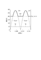
- FIG. 8 is a diagram illustrating an example of the inverter output voltage target value Vinv *.
- the vertical axis represents voltage and the horizontal axis represents time.
- the broken line indicates the voltage waveform of the commercial power system 3
- the solid line indicates the waveform of the inverter output voltage target value Vinv *.
- the inverter device 1 outputs power using the inverter output voltage target value Vinv * shown in FIG. 8 as the voltage target value by the control according to the flowchart of FIG. Therefore, the inverter apparatus 1 outputs the electric power of the voltage according to the waveform of the inverter output voltage target value Vinv * shown in FIG.
- both waves have substantially the same voltage value and frequency, but the phase of the inverter output voltage target value Vinv * is advanced several times with respect to the voltage phase of the commercial power system 3. ing.
- the control processing unit 30 of the present embodiment changes the phase of the inverter output voltage target value Vinv * to the voltage phase of the commercial power system 3 while executing the feedback control of the booster circuit 10 and the inverter circuit 11.
- the phase is advanced about 3 degrees.
- the angle by which the phase of the inverter output voltage target value Vinv * is advanced with respect to the voltage phase of the commercial power system 3 may be several degrees, and is different from the voltage waveform of the commercial power system 3 as will be described later. Is set in a range where the phase is advanced by 90 degrees with respect to the voltage waveform of the commercial power system 3. For example, it is set in a range of values larger than 0 degree and smaller than 10 degrees.
- the second array 40 connected to the second booster circuit 41 is configured to output power at a voltage smaller than the voltage of power output from the first array 2. .
- the boost circuit voltage target value Vo * which is the voltage target value of the power output from both boost circuits 10 and 41, is: It is set as follows. That is, the first DC input voltage detection value Vg.1 by the first array 2 and the second DC input voltage detection value Vg.2 by the second array 40 are compared, and the first DC input voltage detection that is a higher voltage is detected. The value Vg.1 is selected (the above formula (7)). Next, by comparing the selected first DC input voltage detection value Vg.1 with the absolute value of the inverter output voltage target value Vinv * and adopting the higher value, the booster circuit voltage target value Vo * is adopted. Is configured to ask for.
- FIG. 9A, 9B, and 9C are schematic diagrams showing how to obtain the boost circuit voltage target value Vo *.
- FIG. 9A shows the inverter output voltage target value Vinv * and the first DC input voltage detection value Vg.1.
- the portion below 1 has a waveform that follows the first DC input voltage detection value Vg.1.
- FIG. 9B is a diagram illustrating a waveform of the boost circuit voltage target value Vo *.
- the boost circuit voltage target value Vo * has a waveform that follows the absolute value of the inverter output voltage target value Vinv * for the first DC input voltage detection value Vg.1 or more, and the inverter output The portion where the voltage target value Vinv * is equal to or less than the first DC input voltage detection value Vg.1 has a waveform that follows the first DC input voltage detection value Vg.1. Therefore, as shown in the figure, the booster circuit voltage target value Vo * has a minimum voltage value that is the first DC input voltage detection value Vg.1, so that the voltage is higher than the second DC input voltage detection value Vg.2. It is always possible to prevent the voltage from becoming below the first DC input voltage detection value Vg.1. That is, the second booster circuit 41 always performs boosting in order to output power of a voltage according to the booster circuit voltage target value Vo *.
- the power output from the second booster circuit 41 is boosted with reference to the second DC input voltage detection value Vg.2, the power output from the second booster circuit 41 is within a range K in FIG.
- the voltage value is lower than the first DC input voltage detection value Vg.1 and power is supplied only from the first array 2, power supply from the second array 40 cannot be obtained. For this reason, there exists a possibility that the power supply efficiency as both the arrays 2 and 40 may fall.
- the inverter output voltage target value Vinv * is output from the second booster circuit 41 in a range K in which the first DC input voltage detection value Vg.1 or less. Since the second booster circuit 41 is controlled so that the voltage value of the power to be substantially equal to the first DC input voltage detection value Vg.1, the minimum voltage value of the power output from the second booster circuit 41 is 1 DC input voltage detection value Vg.1 can be substantially matched.
- the boost circuit current target value Iin.i * which is the current target value of each boost circuit
- the AC power output from the inverter circuit 11 as shown in the above equation (8).
- a value can be suitably obtained.
- the minimum voltage value of the electric power output from the second booster circuit 41 substantially coincides with the first DC input voltage detection value Vg.1.
- the booster stops during the period in which the inverter output voltage target value Vinv * is lower than the first DC input voltage detection value Vg.1, and the inverter output Boosting is performed during a period in which the voltage target value Vinv * is higher than the first DC input voltage detection value Vg.1.
- the state in which the voltage value of the electric power output from the second booster circuit 41 (second DC input voltage detection value Vg.2) and the first DC input voltage detection value Vg.1 substantially coincide with each other is When power is supplied from the first booster circuit 10 and the second booster circuit 41, it means a state where the voltages match to such an extent that power can be obtained from both.
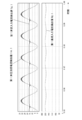
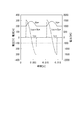
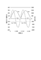
- FIG. 10 is a graph showing the results obtained by simulation over time of the DC input voltage detection values Vg.1, Vg.2 and the booster circuit voltage target value Vo * together with the target values.
- the upper graph shows the relationship between the inverter output voltage target value Vinv * and the system voltage detection value Va
- the middle graph shows the DC input voltage values Vg.1, Vg.2 and the booster circuit.
- the graph showing the relationship with the voltage target value Vo * and the lower graph are graphs showing the boost circuit current target values Iin.1 * and Iin.2 *.
- the booster circuit voltage target value Vo * has a waveform that follows the absolute value of the inverter output voltage target value Vinv * for the first DC input voltage detection value Vg.1 or more, and the inverter output It can be confirmed that the portion where the voltage target value Vinv * is equal to or lower than the first DC input voltage detection value Vg.1 has a waveform following the first DC input voltage detection value Vg.1.
- the first booster circuit control unit 32 (FIG. 3) controls the switching element Qb1 of the first booster circuit 10.
- the inverter circuit control unit 33 controls the switching elements Q1 to Q4 of the inverter circuit 11.
- the first booster circuit control unit 32 and the inverter circuit control unit 33 generate a first booster circuit carrier and an inverter circuit carrier, respectively, and the first booster circuit voltage, which is a target value given from the control processing unit 30, is generated. Modulation is performed using the reference value Vbc1 # and the inverter voltage reference value Vinv #, and a drive waveform for driving each switching element is generated.
- the first booster circuit control unit 32 and the inverter circuit control unit 33 control each switching element based on the drive waveform, thereby generating AC power having a voltage waveform approximate to the waveform of the inverter output voltage target value Vinv * as the first.
- the voltage is output to the booster circuit 10 and the inverter circuit 11.
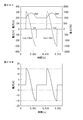
- FIG. 11 is a graph comparing the first booster circuit carrier wave with the waveform of the first booster circuit voltage reference value Vbc1 #.
- the vertical axis represents voltage and the horizontal axis represents time.
- the wavelength of the first booster carrier wave is shown longer than the actual one for easy understanding.
- the booster circuit carrier wave generated by the first booster circuit control unit 32 is a triangular wave whose local minimum value is “0”, and the amplitude A1 is the booster circuit voltage target value Vo * given from the control processing unit 30.
- the frequency of the booster circuit carrier wave is set by the booster circuit control unit 32 according to a control command from the control processing unit 30 so as to have a predetermined duty ratio.
- the booster circuit voltage target value Vo * is the inverter output voltage target during the period W1 in which the absolute value of the inverter output voltage target value Vinv * is approximately equal to or greater than the first DC input voltage detection value Vg.1. It follows the absolute value of the value Vinv * and changes so as to follow the first DC input voltage detection value Vg.1 during the other periods. Therefore, the amplitude A1 of the first booster carrier wave also changes according to the booster circuit voltage target value Vo *.
- the first DC input voltage detection value Vg.1 is 250 volts
- the voltage amplitude of the commercial power system 3 is 288 volts.
- the waveform of the first booster circuit voltage reference value Vbc1 # (hereinafter also referred to as a first booster circuit reference wave Vbc1 #) is a value that the control processing unit 30 obtains based on the booster circuit current target value Iin.1 *.
- the absolute value of the inverter output voltage target value Vinv * is a positive value in the period W1 in which the absolute value is larger than the first DC input voltage detection value Vg.1.
- the first booster circuit reference wave Vbc1 # has a waveform that approximates the waveform formed by the booster circuit voltage target value Vo * in the period W1, and intersects the first booster circuit carrier wave. .
- the first booster circuit control unit 32 compares the first booster circuit carrier wave with the first booster circuit reference wave Vbc1 #, and the first booster circuit reference wave Vbc1 # that is the target value of the voltage across the DC reactor 15.
- a drive waveform for driving the switching element Qb1 is generated so that is turned on when the frequency becomes equal to or higher than the first booster carrier and turned off when equal to or lower than the frequency.
- FIG. 11 is a driving waveform for driving the switching element Qb1 generated by the first booster circuit control unit 32.
- the vertical axis represents voltage and the horizontal axis represents time.
- the horizontal axis is shown to coincide with the horizontal axis in FIG.
- This drive waveform indicates the switching operation of the switching element Qb1, and by applying it to the switching element Qb1, the switching operation according to the drive waveform can be executed.
- the drive waveform constitutes a control command that turns off the switching element when the voltage is 0 volts and turns on the switching element when the voltage is positive.
- the first booster circuit control unit 32 generates a drive waveform such that the switching operation is performed in a range W1 in which the absolute value of the inverter output voltage target value Vinv * is equal to or greater than the first DC input voltage detection value Vg.1. To do. Therefore, the switching element Qb1 is controlled so as to stop the switching operation within the range of the first DC input voltage detection value Vg.1 or less.
- Each pulse width is determined by the intercept of the first booster carrier wave that is a triangular wave. Therefore, the pulse width increases as the voltage increases.
- the first booster circuit control unit 32 modulates the first booster circuit carrier wave with the first booster circuit reference wave Vbc1 #, and generates a drive waveform representing the pulse width for switching.
- the first booster circuit control unit 32 performs PWM control on the switching element Qb1 of the first booster circuit 10 based on the generated drive waveform.
- the switching element Qbu When the switching element Qbu that conducts in the forward direction of the diode in parallel with the diode 16 is installed, the switching element Qbu uses a driving waveform that is inverted from the driving waveform of the switching element Qb. However, in order to prevent the switching element Qb and the switching element Qbu from conducting simultaneously, a dead time of about 1 microsecond is provided when the drive pulse of the switching element Qbu shifts from OFF to ON.
- FIG. 12A is a graph comparing the inverter circuit carrier and the waveform of the inverter voltage reference value Vinv #.
- the vertical axis represents voltage and the horizontal axis represents time.
- the wavelength of the carrier wave for the inverter circuit is shown longer than the actual wavelength for easy understanding.
- the inverter circuit carrier generated by the inverter circuit control unit 33 is a triangular wave having an amplitude center of 0 volts, and its one-side amplitude is set to the boost circuit voltage target value Vo * (the voltage target value of the capacitor 23). Therefore, the amplitude A2 of the carrier wave for the inverter circuit is the first DC input voltage detection value Vg. 1 has a period twice as long (500 volts) and a period twice as long as the voltage of the commercial power system 3 (maximum 576 volts). Further, the frequency is set by the inverter circuit control unit 33 so as to have a predetermined duty ratio by a control command or the like by the control processing unit 30.
- the booster circuit voltage target value Vo * is the inverter output voltage target during the period W1 in which the absolute value of the inverter output voltage target value Vinv * is approximately equal to or greater than the first DC input voltage detection value Vg.1. It follows the absolute value of the value Vinv * and changes so as to follow the first DC input voltage detection value Vg.1 in the other period W2. Therefore, the amplitude A2 of the inverter circuit carrier also changes in accordance with the boost circuit voltage target value Vo *.
- the waveform of the inverter voltage reference value Vinv # (hereinafter also referred to as the inverter circuit reference wave Vinv #) is a value obtained by the control processing unit 30 based on the inverter current target value Iinv *, and is generally a voltage amplitude of the commercial power system 3. It is set to be the same as (288 volts). Therefore, the inverter circuit reference wave Vinv # intersects the inverter circuit carrier in a portion where the voltage value is in the range of ⁇ Vg.1 to + Vg.1.
- the inverter circuit control unit 33 compares the inverter circuit carrier wave with the inverter circuit reference wave Vinv #, and turns on when the inverter circuit reference wave Vinv # is equal to or higher than the inverter circuit carrier wave and turns off when the inverter circuit reference wave Vinv # is equal to or lower than the carrier wave.
- a drive waveform for driving the switching elements Q1 to Q4 is generated so that
- (B) in FIG. 12 is a drive waveform for driving the switching element Q1 generated by the inverter circuit control unit 33.
- the vertical axis represents voltage and the horizontal axis represents time.
- the horizontal axis is shown to coincide with the horizontal axis in FIG.
- the inverter circuit control unit 33 generates a drive waveform so that the switching operation is performed in the range W2 where the voltage of the inverter circuit reference wave Vinv # is in the range of ⁇ Vg.1 to + Vg.1. Therefore, in the other range, the switching element Q1 is controlled so as to stop the switching operation.
- (C) in FIG. 12 is a drive waveform for driving the switching element Q3 generated by the inverter circuit control unit 33.
- the vertical axis represents voltage and the horizontal axis represents time.
- the inverter circuit control unit 33 compares the inverted wave of the inverter circuit reference wave Vinv # indicated by the broken line in the drawing with a carrier wave to generate a drive waveform. Also in this case, the inverter circuit control unit 33 generates the drive waveform so that the switching operation is performed in the range W2 where the voltage of the inverter circuit reference wave Vinv # (the inverted wave thereof) is ⁇ Vg.1 to + Vg.1. To do. Therefore, in the other range, the switching element Q3 is controlled so as to stop the switching operation.
- the inverter circuit control unit 33 generates the inverted driving waveform of the switching element Q1 for the driving waveform of the switching element Q2, and inverts the driving waveform of the switching element Q3 for the driving waveform of the switching element Q4.
- the inverter circuit control unit 33 modulates the inverter circuit carrier wave with the inverter circuit reference wave Vinv #, and generates a drive waveform representing a pulse width for switching.
- the inverter circuit control unit 33 performs PWM control on the switching elements Q1 to Q4 of the inverter circuit 11 based on the generated drive waveform.
- the first booster circuit control unit 32 of the present embodiment outputs power so that the current flowing through the DC reactor 15 matches the booster circuit current target value Iin.1 *.
- the first booster circuit 10 is caused to perform a switching operation in a period W1 (FIG. 11) in which the absolute value of the inverter output voltage target value Vinv * is approximately equal to or greater than the first DC input voltage detection value Vg.1.
- the first booster circuit 10 outputs power so as to approximate a voltage equal to or higher than the first DC input voltage detection value Vg.1 to the absolute value of the inverter output voltage target value Vinv * in the period W1.
- the booster circuit control unit 32 stops the switching operation of the booster circuit 10. Therefore, in the range below the first DC input voltage detection value Vg.1, the first booster circuit 10 outputs the DC power output from the first array 2 to the inverter circuit 11 without boosting.
- the inverter circuit control part 33 of this embodiment outputs electric power so that the electric current which flows into the AC reactor 22 may correspond to inverter electric current target value Iinv *.
- the inverter circuit 11 is caused to perform a switching operation in a range W2 (FIG. 12) where the inverter output voltage target value Vinv * is approximately in the range of ⁇ Vg.1 to + Vg.1. That is, the inverter circuit 11 is caused to perform a switching operation in a period in which the absolute value of the inverter output voltage target value Vinv * is equal to or less than the first DC input voltage detection value Vg.1.
- the inverter circuit 11 performs a switching operation while the first booster circuit 10 stops the switching operation, and outputs an AC voltage that approximates the inverter output voltage target value Vinv *.
- the inverter circuit control unit 33 stops the switching operation of the inverter circuit 11 in a period other than the period W2 in which the inverter output voltage target value Vinv * is approximately ⁇ Vg.1 to + Vg.1.
- the inverter circuit 11 is supplied with power boosted by the first booster circuit 10. Therefore, the inverter circuit 11 that has stopped the switching operation outputs the power supplied from the first booster circuit 10 without stepping down.
- the inverter device 1 performs the switching operation so that the first booster circuit 10 and the inverter circuit 11 are alternately switched, and superimposes the power output from each of them, so that the inverter output voltage target value Vinv * is obtained. Output AC power with approximate voltage waveform.
- the first booster circuit 10 is operated when the voltage higher than the first DC input voltage detection value Vg.1 is output from the AC power output from the inverter device 1.
- the inverter circuit 11 is controlled to operate when outputting a voltage of a portion lower than the first DC input voltage detection value Vg.1. Therefore, since the inverter circuit 11 does not step down the power boosted by the first booster circuit 10, the potential difference when the voltage is stepped down can be kept low, thereby reducing the loss due to switching of the booster circuit, AC power can be output with higher efficiency.
- the booster circuit 10 and the inverter circuit 11 both calculate the inverter output voltage target value Vinv * based on the inverter current target value Iinv * set by the control unit 12, the booster that is output so as to switch alternately. It is possible to suppress a deviation or distortion between the power of the circuit and the power of the inverter circuit.
- the first booster circuit control unit 32 of the control processing unit 30 operates the first booster circuit 10 to a voltage value slightly lower than the first DC input voltage detection value Vg.1, and the first DC input voltage detection value. Control may be made to stop the switching operation when the voltage value is slightly lower than Vg.1. In this case, the current at the portion where the first booster circuit 10 and the inverter circuit 11 are switched by actively providing a portion where the power output from the first booster circuit 10 and the power output from the inverter circuit 11 are superimposed. Waveforms can be connected smoothly.
- the voltage value slightly lower than the first DC input voltage detection value Vg.1 is to smoothly connect the current waveform output from the first booster circuit 10 and the current waveform output from the inverter circuit 11.
- the first DC input voltage detection value Vg. Is a set voltage value so that the output of the first booster circuit 10 and the output of the inverter circuit 11 overlap as much as necessary to smoothly connect both current waveforms. A voltage value set lower than 1.
- FIG. 13 is a diagram illustrating an example of a reference wave and driving waveforms of the switching elements Qb1, Q1 to Q4.
- the reference wave Vinv # and carrier wave of the inverter circuit, the driving waveform of the switching element Q1, the reference wave Vbc1 # and carrier wave of the first booster circuit, the driving waveform of the switching element Qb, and the inverter device 1 The graph which shows the target value and measured value of the current waveform of the alternating current power to output is represented.
- the horizontal axis of each graph indicates time and is shown to coincide with each other.
- the actual measured value Ia of the output current is controlled to coincide with the target value Ia *. It can also be seen that the period of switching operation of the switching element Qb1 of the first booster circuit 10 and the period of switching operation of the switching elements Q1 to Q4 of the inverter circuit 11 are controlled to be switched alternately.
- the second booster circuit control unit 35 (FIG. 3) controls the switching element Qb2 of the second booster circuit 41.
- the second booster circuit control unit 35 generates a second booster circuit carrier wave, modulates the carrier wave with the second booster circuit voltage reference value Vbc2 # supplied from the control processing unit 30, and drives the switching element Qb2. Generate a drive waveform.
- the second booster circuit control unit 35 and the inverter circuit control unit 33 control each switching element based on the drive waveform, and thereby inverter the AC power having a voltage waveform approximate to the waveform of the inverter output voltage target value Vinv *. Output to the circuit 11.
- 14A is a graph comparing the second booster circuit carrier wave with the waveform of the second booster circuit voltage reference value Vbc2 #.
- the vertical axis represents voltage and the horizontal axis represents time.
- the second booster circuit carrier wave generated by the second booster circuit controller 35 is a triangular wave, and its amplitude is set to the same value (amplitude A1) as the voltage amplitude width of the booster circuit voltage target value Vo *.
- the frequency is set by the second booster circuit control unit 35 so as to have a predetermined duty ratio according to a control command or the like by the control processing unit 30. In the present embodiment, it is assumed that the second DC input voltage detection value Vg.2 is 150 volts.
- the booster circuit voltage target value Vo * is the inverter output voltage target value Vinv * during a period in which the absolute value of the inverter output voltage target value Vinv * is approximately equal to or greater than the first DC input voltage detection value Vg.1. In the other period, it changes so as to follow the first DC input voltage detection value Vg.1. Therefore, the amplitude of the second booster carrier wave also changes according to the booster circuit voltage target value Vo *.
- the waveform of the second booster circuit voltage reference value Vbc2 # (hereinafter also referred to as the second booster circuit reference wave Vbc2 #) is a value obtained by the control processing unit 30 based on the booster circuit current target value Iin.2 *. Unlike the first booster circuit reference wave Vbc1 #, the value is substantially positive over the entire area. Therefore, the second booster circuit voltage reference value Vbc2 # intersects over almost the entire area of the second booster circuit carrier wave.
- the second booster circuit control unit 35 compares the second booster circuit carrier with the second booster circuit voltage reference value Vbc2 #, and the second booster circuit voltage reference value Vbc2 # is equal to or higher than the second booster circuit carrier.
- the driving waveform for driving the switching element Qb2 is generated so that the switching element Qb2 is turned on at the portion below the carrier wave for the second booster circuit.
- FIG. 14B shows a drive waveform for driving the switching element Qb2 generated by the second booster circuit control unit 35.
- the vertical axis represents voltage and the horizontal axis represents time.
- the horizontal axis is shown to coincide with the horizontal axis in FIG.
- the second booster circuit voltage reference value Vbc2 # intersects the second booster circuit carrier wave over the entire region. Therefore, the second booster circuit control unit 35 generates a drive waveform so that the switching operation by the switching element Qb2 is performed over the entire region.
- the second booster circuit controller 35 modulates the second booster circuit carrier wave with the second booster circuit voltage reference value Vbc2 #, and generates a drive waveform representing the pulse width for switching.
- the second booster circuit control unit 35 performs PWM control of the switching element Qb2 of the second booster circuit 41 based on the generated drive waveform.
- the second booster circuit 41 outputs a current waveform approximate to the second booster circuit current target value Iin2 * by the control based on the drive waveform.
- the lowest voltage value of the power output from the second booster circuit 41 substantially matches the first DC input voltage detection value Vg.1 (see FIG. 9B), and therefore the power output from the second booster circuit 41. Can be prevented from being significantly lower than the voltage value of the power output by the first booster circuit 10. As a result, it is possible to prevent a period in which power supply from the second array 40 through the second booster circuit 41 cannot be obtained, and to suppress a decrease in power supply efficiency.
- the voltage of the power that the second booster circuit 41 gives to the inverter circuit 11 is the power that the first booster circuit 10 gives to the inverter circuit 11 (the power boosted by the first booster circuit 10 and the DC power that the first array 2 outputs). The voltage is almost the same. Therefore, the power given to the inverter circuit 11 by the second booster circuit 41 is superimposed on the power given to the inverter circuit 11 by the first booster circuit 10 and given to the inverter circuit 11.
- the inverter circuit 11 outputs AC power having a voltage waveform approximate to the inverter output voltage target value Vinv *, as described above, using the power supplied from the booster circuits 10 and 41.
- the inverter output voltage target value Vinv * is generated as a voltage phase advanced by the control processor 30 several times with respect to the voltage phase of the commercial power system 3 as described above. Therefore, the AC voltage output from both the booster circuits 10 and 41 and the inverter circuit 11 is also a voltage phase advanced by several degrees with respect to the voltage phase of the commercial power system 3.
- (A) in FIG. 15 is a graph showing the voltage waveforms of the AC voltage output from the inverter circuit 11, the commercial power system 3, and the voltage across the AC reactor 22, respectively.
- the vertical axis represents voltage and the horizontal axis represents time.
- the voltage of both ends of the AC reactor 22 is a voltage applied to both ends of the AC reactor 22. Difference.
- the phase of the voltage across the AC reactor 22 is advanced by 90 degrees with respect to the voltage phase of the commercial power system 3.
- FIG. 15 is a graph showing a waveform of a current flowing through the AC reactor 22.
- the vertical axis represents current and the horizontal axis represents time.
- the horizontal axis is shown to coincide with the horizontal axis in FIG.
- the current phase of AC reactor 22 is delayed by 90 degrees with respect to the voltage phase. Therefore, as shown in the figure, the current phase of the AC power output through the AC reactor 22 is synchronized with the current phase of the commercial power system 3.
- the voltage phase output from the inverter circuit 11 is advanced several times with respect to the commercial power system 3, but the current phase matches the current phase of the commercial power system 3. Therefore, the current waveform of the AC power output from the inverter device 1 matches the voltage phase of the commercial power system 3.
- the case where the two solar cell arrays of the first array 2 and the second array 40 are connected in parallel to the inverter circuit 11 is illustrated.
- a booster circuit to which the array is connected may be connected.
- the solar cell array having the highest output power voltage value is the first array 2 of the above embodiment
- the other array is the second array 40 of the above embodiment.
- the voltage value at the optimum operating point in the solar cell array having the highest voltage value is set as the first input voltage setting value Vset1
- the lowest voltage value of the power output from the other solar cell arrays is set as the first input voltage setting.
- Other solar cell arrays are controlled so as to substantially match the value Vset1.
- the amplitude of the carrier wave of the inverter circuit, the first booster circuit, and the second booster circuit is the booster circuit voltage target value Vo *.
- a voltage sensor for detecting the voltage across the capacitor 19 is installed. It is also possible to obtain the boost circuit voltage detection value Vo and perform control using this.
- the booster circuit voltage detection value Vo can be used as the amplitude of the carrier wave. As a result, even when the system voltage or the output voltage of the DC power supply fluctuates, an alternating current with less distortion can be output.
- the booster circuit and the inverter circuit perform high-frequency switching for the minimum number of times (minimum switching control).
- the inverter circuit operates avoiding the peak of the absolute value of the AC voltage and its vicinity, and the booster circuit operates avoiding the zero cross of the AC voltage and its vicinity.
- the voltage applied to the element and the reactor is relatively low. This also contributes to the reduction of the switching loss of the semiconductor element and the iron loss of the reactor. Thus, it is possible to reduce the loss of the entire inverter device.
- the inverter circuit and the booster circuit perform high-frequency switching alternately so that the timings of the high-frequency switching do not overlap, but in reality, a slight overlap occurs. However, if there is each stop period, a loss is reduced and it contributes to high efficiency. In addition, as will be described later, switching may be intentionally performed at the same time.
- Inverter device boost circuit, inverter circuit
- Booster circuit (10, 41)
- DC / DC converter (10, 41)
- Inverter circuit (11) ⁇ DC / AC converter (11)
- Ia * target input value from commercial power system 3
- Iin current detection value of DC / DC converter
- Iin * target current value of DC / DC converter
- Iinv * target value of AC input current to DC / AC converter
- Ig * DC input current target value to storage battery
- Va Grid voltage detection value
- Vg Storage battery voltage value
- Vinv * AC input voltage target value to DC / AC converter
- Vo * Input voltage target value to DC / DC converter Pin: Storage battery Input power to
- FIG. 16 is a block diagram illustrating an example of a system in which the power conversion device 1 is provided between the two types of DC power sources 2 and 40 and the AC system 3A.
- the DC power source 2 is a solar cell array.
- the DC power supply 40 is a rechargeable storage battery.
- the internal configuration of the power conversion device 1 is substantially the same as that of the inverter device 1 of FIG. AC system 3A is connected to commercial power system 3 via distribution board 3D in the consumer.
- the distribution board 3D is connected to a load (such as home appliances) 3L used in the consumer.
- the output of the DC power source (solar cell array) 2 is linked to the AC system 3A via the power conversion device 1 to supply power, and surplus power that cannot be used by the load 3L can be sold. Further, the DC power source (storage battery) 40 can be charged by converting the power from the AC system 3 ⁇ / b> A by the power conversion device 1. The DC power supply (storage battery) 40 can be charged by the output of the DC power supply (solar cell array) 2. The DC power supply (storage battery) 40 can supply the stored power to the load 3L.
- FIG. 17 is an example of a circuit diagram of the power conversion device 1 in FIG.
- the difference from FIG. 2 is that, in the DC / DC converter 41 capable of not only stepping up but also stepping down, a switching element Qb3 is provided in place of the diode 43 (FIG. 2), and the AC side is a comprehensive AC system 3A. It is a point expressed in The switching element Qb3 is chopper-controlled by the control unit 12. Since other configurations are the same as those in FIG. 2, the description thereof is omitted here.
- the voltage target value Vo * output to the DC bus 20 is lower than the peak value of the absolute value of the AC voltage of the AC system.
- Vo * is the larger one of the DC input voltage detection value Vg and the absolute value of the voltage target value Vinv * of the DC / AC converter 11 according to the equation (6) or (6s). .
- the DC input voltage detection value Vg becomes the voltage target value Vo *.
- the DC voltage taken out from the solar cell array is, for example, rated 250 V, but varies greatly depending on the state of solar power generation, and decreases to, for example, DC 50 V at the lower side. In the case of storage batteries, the value varies widely depending on the type and manufacturer. Consider the effect of low DC voltage on minimum switching control.
- FIG. 18 is an example of a waveform diagram showing the relationship among the absolute value of the voltage target value Vinv * of the AC voltage, the DC input voltage detection value Vg, and the voltage target value Vo *.
- the number n of DC power supplies is 2
- the DC input voltage detection value Vg that is, the value of Max (Vg.i) is 200 V
- the effective value of Vinv * is 202 V
- the frequency is 60 Hz (period is about 0.0167 seconds).
- the capacitance Co of the smoothing capacitor 19 is 100 ⁇ F.
- FIG. 19 is a waveform diagram showing the voltage target value Vo * (solid line), the reactive current Ico (broken line) flowing through the capacitor 19 and the reactive power (Ico ⁇ Vo *) (dashed line).
- the reactive power (Ico ⁇ Vo *) can be shared by the two DC / DC converters. If the DC / DC converter converts the DC input with the higher voltage, the Ico ⁇ A current burden of Vo * / n / Vg.i is required. This is the case where Ig.i is equal in (Ico ⁇ Vo *) ⁇ Ig.i * / ⁇ ⁇ Ig.i * ⁇ Vg.i>, which is a part of the right side in the above formula (8b). Value.
- FIG. 20 is a waveform diagram showing the reactive current (Ico ⁇ Vo * / n / Vg.i).
- FIG. 21 is another example of a waveform diagram showing the relationship among the absolute value of the voltage target value Vinv * of the AC voltage, the DC input voltage detection value Vg, and the voltage target value Vo *.
- the number n of DC power supplies is 2
- the DC input voltage detection value Vg that is, the value of Max (Vg.i) is 50 V
- the effective value of Vinv * is 202 V
- the frequency is 60 Hz (period is about 0.0167 seconds).
- the capacitance Co of the smoothing capacitor 19 is 100 ⁇ F.
- FIG. 22 is a waveform diagram showing the voltage target value Vo * (solid line), the reactive current Ico (broken line) flowing through the capacitor 19 and the reactive power (Ico ⁇ Vo *) (dashed line).
- the reactive power (Ico ⁇ Vo *) can be shared by the two DC / DC converters. If the DC / DC converter converts the DC input with the higher voltage, the Ico ⁇ A current burden of Vo * / n / Vg.i is required.
- FIG. 23 is a waveform diagram showing this reactive current (Ico ⁇ Vo * / n / Vg.i).
- the value of Vo_limit is set to 200 [V].
- the reactive power generation period is preferably 1 ⁇ 2 cycle ( ⁇ / 2 [rad]) or less, which is a half of AC half cycle. In this case, since the period during which the reactive power is 0 can be ensured by more than half of the AC (1/2) cycle, the effect of suppressing the reactive power is likely to occur.
- FIG. 24 is an example of a waveform diagram showing the relationship among the absolute value of the voltage target value Vinv * of the AC voltage, the DC input voltage detection value Vg, and the voltage target value Vo *.
- the voltage target value Vo * is determined based on the above equation (6x). Therefore, during the period in which the absolute value of Vinv * is equal to or less than Vo_limit, Vo * takes the value of the voltage lower limit value Vo_limit instead of the value of Vg.
- FIG. 25A shows the voltage target value Vo * (solid line), the reactive current Ico (dashed line) and the reactive power (Ico ⁇ Vo *) (dashed line) when the voltage target value Vo * of FIG. 24 is adopted.
- FIG. FIG. 25B is a waveform diagram showing current (Ico ⁇ Vo * / n / Vg.i). In the waveform diagram of FIG. 25B, the peak value is relatively high and is not different from FIG. This is because the denominator Vg.i in the reactive current equation (Ico ⁇ Vo * / n / Vg.i) is 50 V in the case of FIG. 23 and the case of FIG. 25B.
- FIG. 25B when FIG. 25B is compared with FIG. 23, the period during which the current becomes 0 is clearly increased. That is, the period during which the reactive current flows is shortened. Thereby, the reactive power due to the voltage change at both ends of the capacitor 19 connected to the DC bus 20 can be suppressed. As a result, the effective current control that is originally desired can be performed with higher accuracy.
- 26A and 26B are diagrams showing characteristics of MPPT control by the DC / DC converter when a lower limit value is not given to Vo * for comparison.
- “A” represents a voltage-current relationship
- “B” represents power.
- FIG. 26A shows a case where the input voltage is DC65V, and the power point indicated by a black circle is located at the power peak, and therefore MPPT control is performed.
- FIG. 26B shows a case where the input DC voltage is DC 60V, and the power point indicated by the black circle is not located at the power peak, and therefore MPPT control cannot be performed. That is, in the case where the lower limit value is not given to the voltage target value Vo *, an example is shown in which MPPT control cannot be performed when the voltage drops to DC 60V. In the simulation, the MPPT efficiency (taken DC power / power that can be generated) was less than 90%.
- FIGS. 27A and 27B are diagrams showing characteristics of MPPT control by the DC / DC converter 10 when the voltage lower limit value Vo_limit is given to Vo *.
- “A” represents a voltage-current relationship
- “B” represents power.
- FIG. 27A shows a case where the input voltage is DC 60V, and the power point indicated by the black circle is located at the power peak, so that MPPT control is performed.
- FIG. 27B shows a case where the input voltage is 50 VDC, and the power point indicated by the black circle is located at the power peak, so that MPPT control is performed.
- MPPT control can be performed even when the voltage is lowered to DC 60V, and MPPT control is performed even when the voltage is lowered to DC 50V.
- the MPPT efficiency reaches 98% or more.
- the voltage target value (Vo *) of the DC / DC converter takes the larger of the DC voltage lower limit (Vo_limit) and the absolute value of the voltage target value (Vinv *) on the AC side of the DC / AC converter. Waveform.
- the DC voltage lower limit (Vo_limit) is selected so as to shorten the period in which reactive power is generated and increase the period in which reactive power is 0, as shown in FIG. In this case, as described above, even if the reactive power peak value cannot be suppressed, the reactive power can be suppressed by the zero period, so that the active power can be controlled more easily.
Abstract
Provided is a power conversion device in which a control unit thereof determines an output current target value on the basis of an input power value of direct current power and a voltage value of an alternating current system, determines a current target value and a voltage target value of a DC/AC converter on the basis of the output current target value and thereby controls the DC/AC converter circuit, determines a current target value of a DC/DC converter on the basis of the current target value and the voltage target value of the DC/AC converter circuit and the voltage target value of the DC/DC converter and controls the DC/DC converter, thereby controlling the output of alternating current power and selecting, for the voltage target value of the DC/DC converter, the largest value at a given time of one of the following: the direct current voltage value of a direct current power source; the absolute value of the voltage target value on the alternating current side of the DC/AC converter; and the direct current voltage lower limit value, which is a prescribed value less than the peak of the absolute value.
Description
本発明は、電力変換装置及びその制御方法に関する。
本出願は、2015年10月7日出願の日本出願第2015-199521号に基づく優先権を主張し、前記日本出願に記載された全ての記載事項を援用するものである。 The present invention relates to a power conversion device and a control method thereof.
This application claims priority based on Japanese Application No. 2015-199521 filed on Oct. 7, 2015, and incorporates all the description items described in the above Japanese application.
例えば太陽光発電のパワーコンディショナとして用いられる電力変換装置は、直流の発電電力を交流に変換して、商用電力系統へ系統連係する運転を行う。伝統的な電力変換装置では、発電した電圧を、交流側のピーク電圧より高い一定電圧まで昇圧回路で昇圧した後、インバータ回路で交流電圧に変換している。この場合、昇圧回路及びインバータ回路は、常時高速なスイッチング動作を行っている。一方、かかる電力変換装置では、変換効率を向上させることが重要である。そこで、直流側の電圧と交流側の瞬時電圧とを常に比較して、昇圧回路については昇圧が必要な期間のみスイッチング動作させ、インバータ回路については降圧が必要な期間のみスイッチング動作させる、という制御が提案されている(例えば特許文献1,2参照。)。このような制御によって昇圧回路及びインバータ回路にスイッチング動作の休止期間ができると、その分、スイッチング損失等が抑制されるので、変換効率の向上に資することになる。
For example, a power conversion device used as a power conditioner for solar power generation converts a direct-current generated power into an alternating current and performs an operation linked to the commercial power system. In a conventional power converter, the generated voltage is boosted by a booster circuit to a constant voltage higher than the peak voltage on the AC side, and then converted into an AC voltage by an inverter circuit. In this case, the booster circuit and the inverter circuit always perform a high-speed switching operation. On the other hand, in such a power conversion device, it is important to improve the conversion efficiency. Therefore, the DC side voltage and the AC side instantaneous voltage are always compared, and the booster circuit is switched only during the period that requires boosting, and the inverter circuit is switched only during the period that requires stepping down. It has been proposed (see, for example, Patent Documents 1 and 2). When the boosting circuit and the inverter circuit have a rest period of the switching operation by such control, the switching loss and the like are suppressed accordingly, which contributes to the improvement of the conversion efficiency.
本発明は、交流系統と、当該交流系統における交流電圧の絶対値のピーク値より低い電圧を出力する直流電源との間に設けられ、直流/交流の電力変換を行う電力変換装置であって、
前記交流系統に接続されたフィルタ回路と、前記直流電源とDCバスとの間に設けられたDC/DCコンバータと、前記DCバスに接続されたコンデンサと、前記DCバスと、前記フィルタ回路との間に設けられたDC/ACコンバータと、前記DC/DCコンバータ及び前記DC/ACコンバータを制御する制御部とを備え、
前記制御部は、直流電力の入力電力値及び前記交流系統の電圧値に基づいて出力電流目標値を求め、当該出力電流目標値に基づいて前記DC/ACコンバータの電流目標値及び電圧目標値を求めて前記DC/ACコンバータ回路を制御し、かつ、前記DC/ACコンバータの電流目標値及び電圧目標値、並びに、前記DC/DCコンバータの電圧目標値に基づいて、前記DC/DCコンバータの電流目標値を求めて前記DC/DCコンバータを制御することにより、交流電力の出力を制御し、前記制御部は、前記DC/DCコンバータの電圧目標値として、前記直流電源の直流電圧値、前記DC/ACコンバータの交流側の電圧目標値の絶対値、及び、当該絶対値のピーク値より小さい所定値である直流電圧下限値のうち、その時点で最も大きい値を選択する、電力変換装置である。 The present invention is a power conversion device that is provided between an AC system and a DC power source that outputs a voltage lower than the peak value of the absolute value of the AC voltage in the AC system, and performs DC / AC power conversion,
A filter circuit connected to the AC system, a DC / DC converter provided between the DC power supply and a DC bus, a capacitor connected to the DC bus, the DC bus, and the filter circuit. A DC / AC converter provided therebetween, and a controller for controlling the DC / DC converter and the DC / AC converter,
The control unit obtains an output current target value based on an input power value of DC power and a voltage value of the AC system, and calculates a current target value and a voltage target value of the DC / AC converter based on the output current target value. And controlling the DC / AC converter circuit, and based on the current target value and voltage target value of the DC / AC converter, and the voltage target value of the DC / DC converter, the current of the DC / DC converter The control unit controls the output of AC power by obtaining the target value and controlling the DC / DC converter, and the control unit sets the DC voltage value of the DC power source as the voltage target value of the DC / DC converter, the DC / The absolute value of the voltage target value on the AC side of the AC converter and the DC voltage lower limit value that is a predetermined value smaller than the peak value of the absolute value are the largest at that time Selecting have value, a power conversion apparatus.
また、本発明は、交流系統と、当該交流系統における交流電圧の絶対値のピーク値より低い電圧を出力する直流電源との間に設けられ、前記交流系統に接続されたフィルタ回路と、前記直流電源とDCバスとの間に設けられたDC/DCコンバータと、前記DCバスに接続されたコンデンサと、前記DCバスと、前記フィルタ回路との間に設けられたDC/ACコンバータとを有し、直流/交流の電力変換を行う電力変換装置、によって実行される制御方法であって、
基本的制御方法として、直流電力の入力電力値及び前記交流系統の電圧値に基づいて出力電流目標値を求め、当該出力電流目標値に基づいて前記DC/ACコンバータの電流目標値及び電圧目標値を求めて前記DC/ACコンバータ回路を制御し、前記DC/ACコンバータの電流目標値及び電圧目標値、並びに、前記DC/DCコンバータの電圧目標値に基づいて、前記DC/DCコンバータの電流目標値を求めて前記DC/DCコンバータを制御することにより、交流電力の出力を制御し、
拡張的制御方法として、前記制御部は、前記DC/DCコンバータの電圧目標値として、前記直流電源の直流電圧値、前記DC/ACコンバータの交流側の電圧目標値の絶対値、及び、当該絶対値のピーク値より小さい所定値である直流電圧下限値のうち、その時点で最も大きい値を選択する、制御方法である。 The present invention also provides a filter circuit provided between an AC system and a DC power source that outputs a voltage lower than the peak value of the absolute value of the AC voltage in the AC system, and connected to the AC system, and the DC A DC / DC converter provided between a power supply and a DC bus; a capacitor connected to the DC bus; a DC / AC converter provided between the DC bus and the filter circuit; A control method executed by a power conversion device that performs DC / AC power conversion,
As a basic control method, an output current target value is obtained based on an input power value of DC power and a voltage value of the AC system, and a current target value and a voltage target value of the DC / AC converter are calculated based on the output current target value. And the DC / AC converter circuit is controlled, and the current target value and voltage target value of the DC / AC converter and the current target value of the DC / DC converter are determined based on the voltage target value of the DC / DC converter. By controlling the DC / DC converter by obtaining a value, the output of AC power is controlled,
As an extended control method, the control unit includes, as the voltage target value of the DC / DC converter, a DC voltage value of the DC power supply, an absolute value of a voltage target value on the AC side of the DC / AC converter, and the absolute value In this control method, the largest value at that time is selected from the DC voltage lower limit value that is a predetermined value smaller than the peak value.
[本開示が解決しようとする課題]
例えば太陽光発電の場合、電力変換装置に入力される電圧の高低幅が広く、交流電圧の実効値に比べてかなり低い直流電圧が入力される場合もある。このような低い電圧に対して上記のような制御を適用した場合、昇圧回路とインバータ回路とを繋ぐDCバスに接続された平滑用のコンデンサによって大きな無効電力が発生し、これが、制御の精度に多少の影響を与えることがわかってきた。 [Problems to be solved by the present disclosure]
For example, in the case of photovoltaic power generation, the voltage input to the power converter has a wide range, and a DC voltage that is considerably lower than the effective value of the AC voltage may be input. When the above control is applied to such a low voltage, a large reactive power is generated by the smoothing capacitor connected to the DC bus connecting the booster circuit and the inverter circuit, which increases the control accuracy. It has been found to have some effect.
かかる課題に鑑み、本開示は、基本的にスイッチング動作の休止期間を有する制御を行う電力変換装置において、交流電圧の実効値に比べてかなり低い直流電圧が入力される場合にも制御の精度低下を抑制することを目的とする。
In view of such a problem, the present disclosure basically reduces the control accuracy even when a DC voltage that is considerably lower than the effective value of the AC voltage is input in a power conversion device that performs control having a switching operation pause period. It aims at suppressing.
[本開示の効果]
本開示によれば、基本的にスイッチング動作の休止期間を有する制御を行う電力変換装置において、交流電圧の実効値に比べてかなり低い直流電圧が入力される場合にも制御の精度低下を抑制することができる。 [Effects of the present disclosure]
According to the present disclosure, in a power conversion device that basically performs control having an idle period of a switching operation, even when a DC voltage that is considerably lower than the effective value of the AC voltage is input, a reduction in control accuracy is suppressed. be able to.
[実施形態の要旨]
本発明の実施形態の要旨としては、少なくとも以下のものが含まれる。 [Summary of Embodiment]
The gist of the embodiment of the present invention includes at least the following.
本発明の実施形態の要旨としては、少なくとも以下のものが含まれる。 [Summary of Embodiment]
The gist of the embodiment of the present invention includes at least the following.
(1)これは、交流系統と、当該交流系統における交流電圧の絶対値のピーク値より低い電圧を出力する直流電源との間に設けられ、直流/交流の電力変換を行う電力変換装置であって、
前記交流系統に接続されたフィルタ回路と、前記直流電源とDCバスとの間に設けられたDC/DCコンバータと、前記DCバスに接続されたコンデンサと、前記DCバスと、前記フィルタ回路との間に設けられたDC/ACコンバータと、前記DC/DCコンバータ及び前記DC/ACコンバータを制御する制御部とを備え、
前記制御部は、直流電力の入力電力値及び前記交流系統の電圧値に基づいて出力電流目標値を求め、当該出力電流目標値に基づいて前記DC/ACコンバータの電流目標値及び電圧目標値を求めて前記DC/ACコンバータ回路を制御し、かつ、前記DC/ACコンバータの電流目標値及び電圧目標値、並びに、前記DC/DCコンバータの電圧目標値に基づいて、前記DC/DCコンバータの電流目標値を求めて前記DC/DCコンバータを制御することにより、交流電力の出力を制御し、
前記制御部は、前記DC/DCコンバータの電圧目標値として、前記直流電源の直流電圧値、前記DC/ACコンバータの交流側の電圧目標値の絶対値、及び、当該絶対値のピーク値より小さい所定値である直流電圧下限値のうち、その時点で最も大きい値を選択する、電力変換装置である。 (1) This is a power conversion device that is provided between an AC system and a DC power source that outputs a voltage lower than the peak value of the absolute value of the AC voltage in the AC system, and performs DC / AC power conversion. And
A filter circuit connected to the AC system, a DC / DC converter provided between the DC power supply and a DC bus, a capacitor connected to the DC bus, the DC bus, and the filter circuit. A DC / AC converter provided therebetween, and a controller for controlling the DC / DC converter and the DC / AC converter,
The control unit obtains an output current target value based on an input power value of DC power and a voltage value of the AC system, and calculates a current target value and a voltage target value of the DC / AC converter based on the output current target value. And controlling the DC / AC converter circuit, and based on the current target value and voltage target value of the DC / AC converter, and the voltage target value of the DC / DC converter, the current of the DC / DC converter By controlling the DC / DC converter by obtaining a target value, the output of AC power is controlled,
The control unit, as the voltage target value of the DC / DC converter, is smaller than the DC voltage value of the DC power supply, the absolute value of the voltage target value on the AC side of the DC / AC converter, and the peak value of the absolute value. It is a power converter which selects the largest value at the time among the DC voltage lower limit which is a predetermined value.
上記のように構成された電力変換装置では、直流電源の直流電圧値が直流電圧下限値より大きいときは、直流電源の直流電圧値及びDC/ACコンバータの交流側の電圧目標値の絶対値のいずれか大きい方が、その時点での、DC/DCコンバータの電圧目標値となる。この場合、DC/DCコンバータ及びDC/ACコンバータは共に、交流のサイクル内でスイッチングに休止期間が生じる。一方、直流電源の直流電圧値が直流電圧下限値より小さいときは、直流電圧下限値及びDC/ACコンバータの交流側の電圧目標値の絶対値のいずれか大きい方が、その時点での、DC/DCコンバータの電圧目標値となる。従って、DC/DCコンバータの電圧目標値は、直流電圧下限値と、DC/ACコンバータの交流側の電圧目標値の絶対値との、大きい方をとった波形となる。このことは、交流電圧のピーク値に対して直流電圧が低すぎる場合には、DC/DCコンバータを休止させず、昇圧動作させて直流電圧下限値まで上げることを意味する。これにより、DCバスに接続されたコンデンサの両端の電圧変化による無効電力を抑制することができる。その結果、本来行いたい有効電流の制御を、より精度良く行うことができる。従って、基本的にスイッチング動作の休止期間を有する制御を行う電力変換装置において、交流電圧の実効値に比べてかなり低い直流電圧が入力される場合にも制御の精度低下を抑制することができる。
In the power converter configured as described above, when the DC voltage value of the DC power supply is larger than the DC voltage lower limit value, the absolute value of the DC voltage value of the DC power supply and the voltage target value on the AC side of the DC / AC converter The larger one is the voltage target value of the DC / DC converter at that time. In this case, both the DC / DC converter and the DC / AC converter have a pause in switching within the AC cycle. On the other hand, when the DC voltage value of the DC power supply is smaller than the DC voltage lower limit value, the larger one of the DC voltage lower limit value and the absolute value of the voltage target value on the AC side of the DC / AC converter is the DC current value at that time. This is the voltage target value of the DC converter. Therefore, the voltage target value of the DC / DC converter has a waveform that takes the larger one of the DC voltage lower limit value and the absolute value of the voltage target value on the AC side of the DC / AC converter. This means that if the DC voltage is too low with respect to the peak value of the AC voltage, the DC / DC converter is not paused and is boosted to the DC voltage lower limit value. Thereby, the reactive power by the voltage change of the both ends of the capacitor | condenser connected to DC bus can be suppressed. As a result, the effective current control that is originally desired can be performed with higher accuracy. Therefore, in a power conversion device that basically performs control with a switching operation pause period, it is possible to suppress a reduction in control accuracy even when a DC voltage that is considerably lower than the effective value of the AC voltage is input.
(2)また、(1)の電力変換装置において、例えば、前記直流電源及び前記DC/DCコンバータは複数組設けられており、前記直流電源の直流電圧値は複数存在し、複数存在する直流電圧値のうちの最大値が、前記直流電圧下限値と比較される対象となる。
この場合、無効電力を複数のDC/DCコンバータでシェアすることで、1個あたりのDC/DCコンバータの無効電力を低下させることができる。 (2) Further, in the power conversion device of (1), for example, a plurality of sets of the DC power supply and the DC / DC converter are provided, and there are a plurality of DC voltage values of the DC power supply, and a plurality of DC voltages exist. The maximum value among the values is a target to be compared with the DC voltage lower limit value.
In this case, the reactive power of each DC / DC converter can be reduced by sharing the reactive power with a plurality of DC / DC converters.
(3)また、(1)又は(2)の電力変換装置において、例えば、前記直流電圧下限値は、無効電力が発生する期間を短縮して、無効電力が0となる期間を増大させるように選択される。
この場合、無効電力のピーク値を抑制できなくても、0期間によって、無効電力を抑制できるので、有効電力の制御が、より容易になる。 (3) Also, in the power conversion device of (1) or (2), for example, the DC voltage lower limit value shortens the period during which reactive power is generated and increases the period during which reactive power is zero. Selected.
In this case, even if the reactive power peak value cannot be suppressed, the reactive power can be suppressed in the zero period, so that the active power can be controlled more easily.
(4)また、(3)の電力変換装置において、例えば、前記直流電圧下限値は、無効電力が発生する期間が交流(1/2)サイクルの半分以下になるように選択される。
この場合、無効電力が0となる期間を交流(1/2)サイクルの半分以上確保できるので、無効電力の抑制効果が出やすい。 (4) Moreover, in the power conversion device of (3), for example, the DC voltage lower limit value is selected so that the period during which reactive power is generated is less than half of the AC (1/2) cycle.
In this case, since the period during which the reactive power is 0 can be ensured by more than half of the AC (1/2) cycle, the effect of suppressing the reactive power is likely to occur.
(5)一方、方法の観点からは、交流系統と、当該交流系統における交流電圧の絶対値のピーク値より低い電圧を出力する直流電源との間に設けられ、前記交流系統に接続されたフィルタ回路と、前記直流電源とDCバスとの間に設けられたDC/DCコンバータと、前記DCバスに接続されたコンデンサと、前記DCバスと、前記フィルタ回路との間に設けられたDC/ACコンバータとを有し、直流/交流の電力変換を行う電力変換装置、によって実行される制御方法であって、
基本的制御方法として、直流電力の入力電力値及び前記交流系統の電圧値に基づいて出力電流目標値を求め、当該出力電流目標値に基づいて前記DC/ACコンバータの電流目標値及び電圧目標値を求めて前記DC/ACコンバータ回路を制御し、前記DC/ACコンバータの電流目標値及び電圧目標値、並びに、前記DC/DCコンバータの電圧目標値に基づいて、前記DC/DCコンバータの電流目標値を求めて前記DC/DCコンバータを制御することにより、交流電力の出力を制御し、
拡張的制御方法として、前記制御部は、前記DC/DCコンバータの電圧目標値として、前記直流電源の直流電圧値、前記DC/ACコンバータの交流側の電圧目標値の絶対値、及び、当該絶対値のピーク値より小さい所定値である直流電圧下限値のうち、その時点で最も大きい値を選択する、制御方法である。 (5) On the other hand, from the viewpoint of the method, a filter provided between the AC system and a DC power source that outputs a voltage lower than the peak value of the absolute value of the AC voltage in the AC system and connected to the AC system. A circuit, a DC / DC converter provided between the DC power source and the DC bus, a capacitor connected to the DC bus, a DC / AC provided between the DC bus and the filter circuit. A control method executed by a power conversion device that has a converter and performs DC / AC power conversion,
As a basic control method, an output current target value is obtained based on an input power value of DC power and a voltage value of the AC system, and a current target value and a voltage target value of the DC / AC converter are calculated based on the output current target value. And the DC / AC converter circuit is controlled, and the current target value and voltage target value of the DC / AC converter and the current target value of the DC / DC converter are determined based on the voltage target value of the DC / DC converter. By controlling the DC / DC converter by obtaining a value, the output of AC power is controlled,
As an extended control method, the control unit includes, as the voltage target value of the DC / DC converter, a DC voltage value of the DC power supply, an absolute value of a voltage target value on the AC side of the DC / AC converter, and the absolute value In this control method, the largest value at that time is selected from the DC voltage lower limit value that is a predetermined value smaller than the peak value.
上記(5)の制御方法では、直流電源の直流電圧値が直流電圧下限値より大きいときは、直流電源の直流電圧値及びDC/ACコンバータの交流側の電圧目標値の絶対値のいずれか大きい方が、その時点での、DC/DCコンバータの電圧目標値となる。この場合、DC/DCコンバータ及びDC/ACコンバータは共に、交流のサイクル内でスイッチングに休止期間が生じる。一方、直流電源の直流電圧値が直流電圧下限値より小さいときは、直流電圧下限値及びDC/ACコンバータの交流側の電圧目標値の絶対値のいずれか大きい方が、その時点での、DC/DCコンバータの電圧目標値となる。従って、DC/DCコンバータの電圧目標値は、直流電圧下限値と、DC/ACコンバータの交流側の電圧目標値の絶対値との、大きい方をとった波形となる。このことは、交流電圧のピーク値に対して直流電圧が低すぎる場合には、DC/DCコンバータを休止させず、昇圧動作させて直流電圧下限値まで上げることを意味する。これにより、DCバスに接続されたコンデンサの両端の電圧変化による無効電力を抑制することができる。その結果、本来行いたい有効電流の制御を、より精度良く行うことができる。従って、基本的にスイッチング動作の休止期間を有する制御を行う電力変換装置において、交流電圧の実効値に比べてかなり低い直流電圧が入力される場合にも制御の精度低下を抑制することができる。
In the control method of (5) above, when the DC voltage value of the DC power supply is larger than the DC voltage lower limit value, either the DC voltage value of the DC power supply or the absolute value of the voltage target value on the AC side of the DC / AC converter is larger. This is the voltage target value of the DC / DC converter at that time. In this case, both the DC / DC converter and the DC / AC converter have a pause in switching within the AC cycle. On the other hand, when the DC voltage value of the DC power supply is smaller than the DC voltage lower limit value, the larger one of the DC voltage lower limit value and the absolute value of the voltage target value on the AC side of the DC / AC converter is the DC current value at that time. This is the voltage target value of the DC converter. Therefore, the voltage target value of the DC / DC converter has a waveform that takes the larger one of the DC voltage lower limit value and the absolute value of the voltage target value on the AC side of the DC / AC converter. This means that if the DC voltage is too low with respect to the peak value of the AC voltage, the DC / DC converter is not paused and is boosted to the DC voltage lower limit value. Thereby, the reactive power by the voltage change of the both ends of the capacitor | condenser connected to DC bus can be suppressed. As a result, the effective current control that is originally desired can be performed with higher accuracy. Therefore, in a power conversion device that basically performs control with a switching operation pause period, it is possible to suppress a reduction in control accuracy even when a DC voltage that is considerably lower than the effective value of the AC voltage is input.
なお、電力変換装置は、(1)及び(4)の表現とは別に、以下のように表現することもできる。
交流系統と、当該交流系統における交流電圧の絶対値のピーク値より低い電圧を出力する直流電源との間に設けられ、直流/交流の電力変換を行う電力変換装置であって、前記交流系統に接続されたフィルタ回路と、前記直流電源とDCバスとの間に設けられたDC/DCコンバータと、前記DCバスに接続されたコンデンサと、前記DCバスと、前記フィルタ回路との間に設けられたDC/ACコンバータと、前記DC/DCコンバータ及び前記DC/ACコンバータを制御する制御部とを備え、
前記制御部は、直流電力の入力電力値及び前記交流系統の電圧値に基づいて出力電流目標値を求め、当該出力電流目標値に基づいて前記DC/ACコンバータの電流目標値及び電圧目標値を求めて前記DC/ACコンバータ回路を制御し、かつ、前記DC/ACコンバータの電流目標値及び電圧目標値、並びに、前記DC/DCコンバータの電圧目標値に基づいて、前記DC/DCコンバータの電流目標値を求めて前記DC/DCコンバータを制御することにより、交流電力の出力を制御し、
前記制御部は、前記DC/DCコンバータの電圧目標値として、前記直流電源の直流電圧値、前記DC/ACコンバータの交流側の電圧目標値の絶対値、及び、当該絶対値のピーク値より小さい所定値である直流電圧下限値のうち、その時点で最も大きい値を選択し、かつ、前記絶対値の脈流波形の一部が現れる期間を脈流1サイクルにおける半分以下にする、電力変換装置である。 In addition, a power converter device can also be expressed as follows separately from the expressions (1) and (4).
A power conversion device that is provided between an AC system and a DC power source that outputs a voltage lower than the peak value of the absolute value of the AC voltage in the AC system, and performs DC / AC power conversion. Provided between the connected filter circuit, a DC / DC converter provided between the DC power source and the DC bus, a capacitor connected to the DC bus, the DC bus, and the filter circuit. A DC / AC converter, and a controller for controlling the DC / DC converter and the DC / AC converter,
The control unit obtains an output current target value based on an input power value of DC power and a voltage value of the AC system, and calculates a current target value and a voltage target value of the DC / AC converter based on the output current target value. And controlling the DC / AC converter circuit, and based on the current target value and voltage target value of the DC / AC converter, and the voltage target value of the DC / DC converter, the current of the DC / DC converter By controlling the DC / DC converter by obtaining a target value, the output of AC power is controlled,
The control unit, as the voltage target value of the DC / DC converter, is smaller than the DC voltage value of the DC power supply, the absolute value of the voltage target value on the AC side of the DC / AC converter, and the peak value of the absolute value. A power conversion device that selects a maximum value of DC voltage lower limit values that are predetermined values at that time and makes a period during which a part of the pulsating waveform of the absolute value appears is less than half of one cycle of pulsating flow It is.
[実施形態の詳細]
以下、本発明の実施形態について図面を参照しながら説明する。
《1 全体構成について》
図1は、一実施形態に係るインバータ装置を備えたシステムの一例を示すブロック図である。図中、インバータ装置1の入力端には、直流電源としての第1太陽電池アレイ2及び第2太陽電池アレイ40が接続され、出力端には、交流の商用電力系統3が接続されている。
このシステムは、第1太陽電池アレイ2(以下、単に第1アレイ2ともいう)及び第2太陽電池アレイ40(以下、単に第2アレイ40ともいう)が発電する直流電力を交流電力に変換し、商用電力系統3に出力する連系運転を行う。 [Details of the embodiment]
Hereinafter, embodiments of the present invention will be described with reference to the drawings.
<< 1 Overall configuration >>
FIG. 1 is a block diagram illustrating an example of a system including an inverter device according to an embodiment. In the figure, the firstsolar cell array 2 and the second solar cell array 40 as DC power sources are connected to the input terminal of the inverter device 1, and the AC commercial power system 3 is connected to the output terminal.
This system converts DC power generated by the first solar cell array 2 (hereinafter also simply referred to as the first array 2) and the second solar cell array 40 (hereinafter also simply referred to as the second array 40) into AC power. Then, an interconnection operation for outputting to thecommercial power system 3 is performed.
以下、本発明の実施形態について図面を参照しながら説明する。
《1 全体構成について》
図1は、一実施形態に係るインバータ装置を備えたシステムの一例を示すブロック図である。図中、インバータ装置1の入力端には、直流電源としての第1太陽電池アレイ2及び第2太陽電池アレイ40が接続され、出力端には、交流の商用電力系統3が接続されている。
このシステムは、第1太陽電池アレイ2(以下、単に第1アレイ2ともいう)及び第2太陽電池アレイ40(以下、単に第2アレイ40ともいう)が発電する直流電力を交流電力に変換し、商用電力系統3に出力する連系運転を行う。 [Details of the embodiment]
Hereinafter, embodiments of the present invention will be described with reference to the drawings.
<< 1 Overall configuration >>
FIG. 1 is a block diagram illustrating an example of a system including an inverter device according to an embodiment. In the figure, the first
This system converts DC power generated by the first solar cell array 2 (hereinafter also simply referred to as the first array 2) and the second solar cell array 40 (hereinafter also simply referred to as the second array 40) into AC power. Then, an interconnection operation for outputting to the
第1アレイ2及び第2アレイ40は、複数の太陽光発電パネル(モジュール)を直並列に接続して構成されている。本実施形態では、第2アレイ40は、当該第2アレイ40が出力する電力の電圧が、第1アレイ2が出力する電力の電圧よりも小さくなるような構成とされている。
The first array 2 and the second array 40 are configured by connecting a plurality of photovoltaic power generation panels (modules) in series and parallel. In the present embodiment, the second array 40 is configured such that the power voltage output from the second array 40 is smaller than the power voltage output from the first array 2.
インバータ装置1は、第1アレイ2が出力する直流電力が与えられる第1昇圧回路10と、第2アレイ40が出力する直流電力が与えられる第2昇圧回路41と、両昇圧回路10,41からDCバス20に出力される電力を交流電力に変換して商用電力系統3に出力するインバータ回路11と、これらの回路10,11,42の動作を制御する制御部12とを備えている。
第1昇圧回路10と、第2昇圧回路41とは、インバータ回路11に対して並列に接続されている。 Theinverter device 1 includes a first booster circuit 10 to which DC power output from the first array 2 is applied, a second booster circuit 41 to which DC power output from the second array 40 is applied, and both booster circuits 10 and 41. An inverter circuit 11 that converts electric power output to the DC bus 20 into AC power and outputs it to the commercial power system 3, and a control unit 12 that controls operations of these circuits 10, 11, 42 are provided.
Thefirst booster circuit 10 and the second booster circuit 41 are connected in parallel to the inverter circuit 11.
第1昇圧回路10と、第2昇圧回路41とは、インバータ回路11に対して並列に接続されている。 The
The
図2は、インバータ装置1の回路図の一例である。
第1アレイ2が接続されている第1昇圧回路10は、直流リアクトル15と、ダイオード16と、IGBT(Insulated Gate Bipolar Transistor)等からなるスイッチング素子Qb1とを備えており、昇圧チョッパ回路を構成している。なお、ダイオード16は、スイッチング素子に代えてもよい。
第1昇圧回路10の入力側には、第1電圧センサ17、第1電流センサ18、及び平滑化のためのコンデンサ26が設けられている。第1電圧センサ17は、第1アレイ2が出力し、第1昇圧回路10に入力される直流電力の第1直流入力電圧検出値Vg.1(直流入力電圧値)を検出し、制御部12に出力する。第1電流センサ18は、直流リアクトル15に流れる電流である第1昇圧回路電流検出値Iin.1を検出し、制御部12に出力する。 FIG. 2 is an example of a circuit diagram of theinverter device 1.
Thefirst booster circuit 10 to which the first array 2 is connected includes a DC reactor 15, a diode 16, and a switching element Qb1 made of an IGBT (Insulated Gate Bipolar Transistor) or the like, and constitutes a boost chopper circuit. ing. The diode 16 may be replaced with a switching element.
Afirst voltage sensor 17, a first current sensor 18, and a smoothing capacitor 26 are provided on the input side of the first booster circuit 10. The first voltage sensor 17 detects the first DC input voltage detection value Vg.1 (DC input voltage value) of the DC power output from the first array 2 and input to the first booster circuit 10, and the control unit 12. Output to. The first current sensor 18 detects a first booster circuit current detection value Iin.1 that is a current flowing through the DC reactor 15, and outputs it to the control unit 12.
第1アレイ2が接続されている第1昇圧回路10は、直流リアクトル15と、ダイオード16と、IGBT(Insulated Gate Bipolar Transistor)等からなるスイッチング素子Qb1とを備えており、昇圧チョッパ回路を構成している。なお、ダイオード16は、スイッチング素子に代えてもよい。
第1昇圧回路10の入力側には、第1電圧センサ17、第1電流センサ18、及び平滑化のためのコンデンサ26が設けられている。第1電圧センサ17は、第1アレイ2が出力し、第1昇圧回路10に入力される直流電力の第1直流入力電圧検出値Vg.1(直流入力電圧値)を検出し、制御部12に出力する。第1電流センサ18は、直流リアクトル15に流れる電流である第1昇圧回路電流検出値Iin.1を検出し、制御部12に出力する。 FIG. 2 is an example of a circuit diagram of the
The
A
第2アレイ40が接続されている第2昇圧回路41は、直流リアクトル42と、ダイオード43と、IGBT等からなるスイッチング素子Qb2とを備えており、第1昇圧回路と同様、昇圧チョッパ回路を構成している。なお、ダイオード43は、スイッチング素子に代えてもよい。
また、第2昇圧回路41の入力側には、第2電圧センサ44、第2電流センサ45、及び平滑化のためのコンデンサ46が設けられている。第2電圧センサ44は、第2アレイ40が出力し、第2昇圧回路41に入力される直流電力の第2直流入力電圧検出値Vg.2を検出し、制御部12に出力する。と、第2電流センサ45は、直流リアクトル42に流れる電流である第2昇圧回路電流検出値Iin.2を検出し、制御部12に出力する。 Thesecond booster circuit 41 to which the second array 40 is connected includes a DC reactor 42, a diode 43, and a switching element Qb2 made of IGBT or the like, and constitutes a boost chopper circuit like the first booster circuit. is doing. The diode 43 may be replaced with a switching element.
Asecond voltage sensor 44, a second current sensor 45, and a smoothing capacitor 46 are provided on the input side of the second booster circuit 41. The second voltage sensor 44 outputs a second DC input voltage detection value Vg. Of DC power output from the second array 40 and input to the second booster circuit 41. 2 is detected and output to the control unit 12. Then, the second current sensor 45 detects the second booster circuit current detection value Iin.2, which is a current flowing through the DC reactor 42, and outputs it to the control unit 12.
また、第2昇圧回路41の入力側には、第2電圧センサ44、第2電流センサ45、及び平滑化のためのコンデンサ46が設けられている。第2電圧センサ44は、第2アレイ40が出力し、第2昇圧回路41に入力される直流電力の第2直流入力電圧検出値Vg.2を検出し、制御部12に出力する。と、第2電流センサ45は、直流リアクトル42に流れる電流である第2昇圧回路電流検出値Iin.2を検出し、制御部12に出力する。 The
A
制御部12は、直流入力電圧検出値Vg.1,Vg.2及び昇圧回路電流検出値Iin.1,Iin.2から入力電力Pin.1、Pin.2を演算し、第1アレイ2及び第2アレイ40に対するMPPT(Maximum Power Point Tracking:最大電力点追従)制御を行う機能を有している。
The control unit 12 calculates input powers Pin.1 and Pin.2 from the DC input voltage detection values Vg.1, Vg.2 and the booster circuit current detection values Iin.1, Iin.2, and the first array 2 and the first array 2 It has a function to perform MPPT (Maximum Power Point Tracking) control for the two arrays 40.
また、第1昇圧回路10のスイッチング素子Qb1は、後述するように、インバータ回路11との間でスイッチング動作を行う期間が交互に切り替わるように、制御部12によって制御される。よって、第1昇圧回路10は、スイッチング動作を行っている期間は、昇圧された電力をインバータ回路11に出力し、スイッチング動作を停止している期間は、第1アレイ2が出力して第1昇圧回路10に入力される直流電力について昇圧を行うことなくインバータ回路11に出力する。
Further, the switching element Qb1 of the first booster circuit 10 is controlled by the control unit 12 so that the period for performing the switching operation with the inverter circuit 11 is alternately switched as described later. Therefore, the first booster circuit 10 outputs the boosted power to the inverter circuit 11 during the period when the switching operation is performed, and the first array 2 outputs the first power during the period when the switching operation is stopped. The DC power input to the booster circuit 10 is output to the inverter circuit 11 without being boosted.
さらに、第2昇圧回路41は、後述するように、所定期間において、第2アレイ40から与えられる直流電力の電圧値を、第1アレイ2から与えられる直流電力の電圧値である第1直流入力電圧検出値Vg.1とほぼ一致する値にまで昇圧して出力するように、制御部12によって制御される。
Further, as will be described later, the second booster circuit 41 converts the voltage value of the DC power supplied from the second array 40 into the first DC input that is the voltage value of the DC power supplied from the first array 2 during a predetermined period. Control is performed by the control unit 12 so that the voltage is boosted to a value substantially equal to the detected voltage value Vg.1 and output.
両昇圧回路10,41と、インバータ回路11との間には、平滑用のコンデンサ19が接続されている。
インバータ回路11は、FET(Field Effect Transistor)からなるスイッチング素子Q1~Q4を備えている。これらスイッチング素子Q1~Q4は、フルブリッジ回路を構成している。
各スイッチング素子Q1~Q4は、制御部12に接続されており、制御部12により制御可能とされている。制御部12は、各スイッチング素子Q1~Q4の動作をPWM制御する。これにより、インバータ回路11は、両昇圧回路10,41から与えられる電力を交流電力に変換する。 A smoothingcapacitor 19 is connected between the booster circuits 10 and 41 and the inverter circuit 11.
Theinverter circuit 11 includes switching elements Q1 to Q4 made of FET (Field Effect Transistor). These switching elements Q1 to Q4 constitute a full bridge circuit.
Each of the switching elements Q1 to Q4 is connected to thecontrol unit 12, and can be controlled by the control unit 12. The control unit 12 performs PWM control of the operations of the switching elements Q1 to Q4. Thereby, the inverter circuit 11 converts the electric power given from both the booster circuits 10 and 41 into alternating current power.
インバータ回路11は、FET(Field Effect Transistor)からなるスイッチング素子Q1~Q4を備えている。これらスイッチング素子Q1~Q4は、フルブリッジ回路を構成している。
各スイッチング素子Q1~Q4は、制御部12に接続されており、制御部12により制御可能とされている。制御部12は、各スイッチング素子Q1~Q4の動作をPWM制御する。これにより、インバータ回路11は、両昇圧回路10,41から与えられる電力を交流電力に変換する。 A smoothing
The
Each of the switching elements Q1 to Q4 is connected to the
インバータ装置1は、インバータ回路11と、商用電力系統3との間にフィルタ回路21を備えている。
フィルタ回路21は、2つの交流リアクトル22と、コンデンサ23とを備えて構成されている。フィルタ回路21は、インバータ回路11から出力される交流電力に含まれる高周波成分を除去する機能を有している。フィルタ回路21により高周波成分が除去された交流電力は、商用電力系統3に与えられる。 Theinverter device 1 includes a filter circuit 21 between the inverter circuit 11 and the commercial power system 3.
Thefilter circuit 21 includes two AC reactors 22 and a capacitor 23. The filter circuit 21 has a function of removing high-frequency components contained in the AC power output from the inverter circuit 11. The AC power from which the high frequency component has been removed by the filter circuit 21 is supplied to the commercial power system 3.
フィルタ回路21は、2つの交流リアクトル22と、コンデンサ23とを備えて構成されている。フィルタ回路21は、インバータ回路11から出力される交流電力に含まれる高周波成分を除去する機能を有している。フィルタ回路21により高周波成分が除去された交流電力は、商用電力系統3に与えられる。 The
The
また、フィルタ回路21には、インバータ回路11による出力の電流値であるインバータ電流検出値Iinv(交流リアクトル22に流れる電流)を検出するための第3電流センサ24が接続されている。さらに、フィルタ回路21と、商用電力系統3との間には、商用電力系統3側の電圧値(系統電圧検出値Va)を検出するための第3電圧センサ25が接続されている。
The filter circuit 21 is connected to a third current sensor 24 for detecting an inverter current detection value Iinv (current flowing through the AC reactor 22), which is a current value output from the inverter circuit 11. Further, a third voltage sensor 25 for detecting a voltage value (system voltage detection value Va) on the commercial power system 3 side is connected between the filter circuit 21 and the commercial power system 3.
第3電流センサ24及び第3電圧センサ25は、検出したインバータ電流検出値Iinv及び系統電圧検出値Vaを制御部12に出力する。
制御部12は、これら系統電圧検出値Va及びインバータ電流検出値Iinvと、上述の直流入力電圧検出値Vg.1,Vg.2、昇圧回路電流検出値Iin.1,Iin.2に基づいて、両昇圧回路10,41及びインバータ回路11を制御する。 The thirdcurrent sensor 24 and the third voltage sensor 25 output the detected inverter current detection value Iinv and the system voltage detection value Va to the control unit 12.
Based on the system voltage detection value Va and the inverter current detection value Iinv, the DC input voltage detection values Vg.1, Vg.2, and the booster circuit current detection values Iin.1, Iin. Both booster circuits 10 and 41 and the inverter circuit 11 are controlled.
制御部12は、これら系統電圧検出値Va及びインバータ電流検出値Iinvと、上述の直流入力電圧検出値Vg.1,Vg.2、昇圧回路電流検出値Iin.1,Iin.2に基づいて、両昇圧回路10,41及びインバータ回路11を制御する。 The third
Based on the system voltage detection value Va and the inverter current detection value Iinv, the DC input voltage detection values Vg.1, Vg.2, and the booster circuit current detection values Iin.1, Iin. Both
《2 制御部について》
図3は、制御部12のブロック図である。制御部12は、図3に示すように、制御処理部30と、第1昇圧回路制御部32と、インバータ回路制御部33と、平均化処理部34と、第2昇圧回路制御部35とを機能的に有している。
制御部12の各機能は、その一部又は全部がハードウェア回路によって構成されてもよいし、その一部又は全部が、ソフトウェア(コンピュータプログラム)をコンピュータによって実行させることで実現されていてもよい。制御部12の機能を実現するソフトウェア(コンピュータプログラム)は、コンピュータの記憶装置(図示省略)に格納される。 << 2 Control section >>
FIG. 3 is a block diagram of thecontrol unit 12. As shown in FIG. 3, the control unit 12 includes a control processing unit 30, a first boost circuit control unit 32, an inverter circuit control unit 33, an averaging processing unit 34, and a second boost circuit control unit 35. Has functionally.
A part or all of the functions of thecontrol unit 12 may be configured by a hardware circuit, or part or all of the functions may be realized by causing a computer (computer program) to be executed by a computer. . Software (computer program) for realizing the function of the control unit 12 is stored in a storage device (not shown) of the computer.
図3は、制御部12のブロック図である。制御部12は、図3に示すように、制御処理部30と、第1昇圧回路制御部32と、インバータ回路制御部33と、平均化処理部34と、第2昇圧回路制御部35とを機能的に有している。
制御部12の各機能は、その一部又は全部がハードウェア回路によって構成されてもよいし、その一部又は全部が、ソフトウェア(コンピュータプログラム)をコンピュータによって実行させることで実現されていてもよい。制御部12の機能を実現するソフトウェア(コンピュータプログラム)は、コンピュータの記憶装置(図示省略)に格納される。 << 2 Control section >>
FIG. 3 is a block diagram of the
A part or all of the functions of the
第1昇圧回路制御部32は、制御処理部30から与えられる目標値と検出値に基づいて、第1昇圧回路10のスイッチング素子Qb1を制御し、前記目標値に応じた電流の電力を第1昇圧回路10に出力させる。
第2昇圧回路制御部35は、制御処理部30から与えられる目標値と検出値に基づいて、第2昇圧回路41のスイッチング素子Qb2を制御し、前記目標値に応じた電流の電力を第2昇圧回路41に出力させる。
また、インバータ回路制御部33は、制御処理部30から与えられる目標値と検出値に基づいて、インバータ回路11のスイッチング素子Q1~Q4を制御し、前記目標値に応じた電流の電力をインバータ回路11に出力させる。 The first boostercircuit control unit 32 controls the switching element Qb1 of the first booster circuit 10 based on the target value and the detection value given from the control processing unit 30, and the power of the current corresponding to the target value is the first. The voltage is output to the booster circuit 10.
The second boostercircuit control unit 35 controls the switching element Qb2 of the second booster circuit 41 based on the target value and the detection value given from the control processing unit 30, and the second power is supplied to the current corresponding to the target value. The voltage is output to the booster circuit 41.
Further, the inverter circuit control unit 33 controls the switching elements Q1 to Q4 of theinverter circuit 11 based on the target value and the detection value given from the control processing unit 30, and the electric power of the current corresponding to the target value is converted to the inverter circuit. 11 to output.
第2昇圧回路制御部35は、制御処理部30から与えられる目標値と検出値に基づいて、第2昇圧回路41のスイッチング素子Qb2を制御し、前記目標値に応じた電流の電力を第2昇圧回路41に出力させる。
また、インバータ回路制御部33は、制御処理部30から与えられる目標値と検出値に基づいて、インバータ回路11のスイッチング素子Q1~Q4を制御し、前記目標値に応じた電流の電力をインバータ回路11に出力させる。 The first booster
The second booster
Further, the inverter circuit control unit 33 controls the switching elements Q1 to Q4 of the
制御処理部30には、直流入力電圧検出値Vg.1,Vg.2、昇圧回路電流検出値Iin.1,Iin.2、系統電圧検出値Va、及びインバータ電流検出値Iinvが与えられる。
制御処理部30は、直流入力電圧検出値Vg.1,Vg.2及び昇圧回路電流検出値Iin.1,Iin.2から、第1昇圧回路10の第1入力電力Pin.1及びその平均値〈Pin.1〉、並びに、第2昇圧回路41の第2入力電力Pin.2及びその平均値〈Pin.2〉を演算する。
制御処理部30は、第1入力電力平均値〈Pin.1〉に基づいて、第1昇圧回路10の第1直流入力電流目標値Ig.1*(後に説明する)を設定し、第1アレイ2についてMPPT制御を行うとともに、第1昇圧回路10及びインバータ回路11それぞれをフィードバック制御する機能を有している。
また、制御処理部30は、第2入力電力平均値〈Pin.2〉に基づいて、第2昇圧回路41の直流入力電流目標値Ig.2*(後に説明する)を設定し、第2アレイ40についてMPPT制御を行うとともに、第2昇圧回路41をフィードバック制御する機能も有している。 Thecontrol processing unit 30 is provided with DC input voltage detection values Vg.1, Vg.2, booster circuit current detection values Iin.1, Iin.2, system voltage detection value Va, and inverter current detection value Iinv.
Thecontrol processing unit 30 calculates the first input power Pin.1 and the average value of the first booster circuit 10 from the DC input voltage detection values Vg.1, Vg.2 and the booster circuit current detection values Iin.1, Iin.2. <Pin.1>, the second input power Pin.2 of the second booster circuit 41, and its average value <Pin.2> are calculated.
Thecontrol processing unit 30 sets a first DC input current target value Ig.1 * (described later) of the first booster circuit 10 based on the first input power average value <Pin.1>, and the first array 2 has a function of performing MPPT control and feedback control of each of the first booster circuit 10 and the inverter circuit 11.
Further, thecontrol processing unit 30 sets a DC input current target value Ig.2 * (described later) of the second booster circuit 41 based on the second input power average value <Pin.2>, and the second array MPPT control is performed for 40, and the second booster circuit 41 is also feedback controlled.
制御処理部30は、直流入力電圧検出値Vg.1,Vg.2及び昇圧回路電流検出値Iin.1,Iin.2から、第1昇圧回路10の第1入力電力Pin.1及びその平均値〈Pin.1〉、並びに、第2昇圧回路41の第2入力電力Pin.2及びその平均値〈Pin.2〉を演算する。
制御処理部30は、第1入力電力平均値〈Pin.1〉に基づいて、第1昇圧回路10の第1直流入力電流目標値Ig.1*(後に説明する)を設定し、第1アレイ2についてMPPT制御を行うとともに、第1昇圧回路10及びインバータ回路11それぞれをフィードバック制御する機能を有している。
また、制御処理部30は、第2入力電力平均値〈Pin.2〉に基づいて、第2昇圧回路41の直流入力電流目標値Ig.2*(後に説明する)を設定し、第2アレイ40についてMPPT制御を行うとともに、第2昇圧回路41をフィードバック制御する機能も有している。 The
The
The
Further, the
直流入力電圧検出値Vg.1,Vg.2及び昇圧回路電流検出値Iin.1,Iin.2は、平均化処理部34、及び制御処理部30に与えられる。
The DC input voltage detection values Vg.1, Vg.2 and the booster circuit current detection values Iin.1, Iin.2 are given to the averaging processing unit 34 and the control processing unit 30.
平均化処理部34は、両電圧センサ17,44及び両電流センサ18,45から与えられる直流入力電圧検出値Vg.1,Vg.2及び昇圧回路電流検出値Iin.1,Iin.2を、予め設定された所定の時間間隔ごとにサンプリングし、それぞれの平均値を求め、平均化された直流入力電圧検出値Vg.1,Vg.2及び昇圧回路電流検出値Iin.1,Iin.2を制御処理部30に与える機能を有している。
The averaging processing unit 34 obtains the DC input voltage detection values Vg.1, Vg.2 and the booster circuit current detection values Iin.1, Iin.2 given from the voltage sensors 17, 44 and the current sensors 18, 45, Sampling is performed at predetermined time intervals set in advance, and the respective average values are obtained, and the averaged DC input voltage detection values Vg.1, Vg.2 and booster circuit current detection values Iin.1, Iin.2 are obtained. It has a function to be given to the control processing unit 30.
図4は、第1直流入力電圧検出値Vg.1、及び第1昇圧回路電流検出値Iin.1の経時変化をシミュレーションにより求めた結果の一例を示すグラフである。
第1昇圧回路電流検出値Iin.1は、後述するように、目標値に基づいて系統電圧と同期した波形として現れている。
また、第1直流入力電流検出値Ig.1は、コンデンサ26よりも入力側で検出される電流値である。 FIG. 4 is a graph showing an example of results obtained by simulating changes with time of the first DC input voltage detection value Vg.1 and the first booster circuit current detection value Iin.1.
The first booster circuit current detection value Iin.1 appears as a waveform synchronized with the system voltage based on the target value, as will be described later.
Further, the first DC input current detection value Ig.1 is a current value detected on the input side from thecapacitor 26.
第1昇圧回路電流検出値Iin.1は、後述するように、目標値に基づいて系統電圧と同期した波形として現れている。
また、第1直流入力電流検出値Ig.1は、コンデンサ26よりも入力側で検出される電流値である。 FIG. 4 is a graph showing an example of results obtained by simulating changes with time of the first DC input voltage detection value Vg.1 and the first booster circuit current detection value Iin.1.
The first booster circuit current detection value Iin.1 appears as a waveform synchronized with the system voltage based on the target value, as will be described later.
Further, the first DC input current detection value Ig.1 is a current value detected on the input side from the
図4に示すように、第1直流入力電圧検出値Vg.1、及び第1直流入力電流検出値Ig.1(第1昇圧回路電流検出値Iin.1)は、系統電圧の1/2の周期で変動していることが判る。
As shown in FIG. 4, the first DC input voltage detection value Vg.1 and the first DC input current detection value Ig.1 (first boost circuit current detection value Iin.1) are half of the system voltage. It turns out that it fluctuates with a period.
図4に示すように、第1直流入力電圧検出値Vg.1、及び第1直流入力電流検出値Ig.1が周期的に変動する理由は、次の通りである。すなわち、インバータ装置1の第1昇圧回路電流検出値Iin.1は、昇圧回路10、及びインバータ回路11の動作に応じて、交流周期の1/2周期でほぼ0Aからピーク値まで大きく変動する。そのため、コンデンサ26で変動成分を完全に取り除くことができず、第1直流入力電流検出値Ig.1は、交流周期の1/2周期で変動する成分を含む脈流となる。一方、太陽光発電パネルは出力電流によって出力電圧が変化する。
よって、第1直流入力電圧検出値Vg.1に生じる周期的な変動は、インバータ装置1が出力する交流電力の1/2周期となっている。つまり、商用電力系統3の1/2周期となっている。 As shown in FIG. 4, the reason why the first DC input voltage detection value Vg.1 and the first DC input current detection value Ig.1 periodically change is as follows. That is, the first booster circuit current detection value Iin.1 of theinverter device 1 greatly fluctuates from approximately 0 A to a peak value in a half cycle of the AC cycle according to the operations of the booster circuit 10 and the inverter circuit 11. Therefore, the fluctuation component cannot be completely removed by the capacitor 26, and the first DC input current detection value Ig.1 becomes a pulsating flow including a component that fluctuates in a half cycle of the AC cycle. On the other hand, the output voltage of the photovoltaic power generation panel changes depending on the output current.
Therefore, the periodic fluctuation occurring in the first DC input voltage detection value Vg.1 is a half cycle of the AC power output from theinverter device 1. That is, it is a half cycle of the commercial power system 3.
よって、第1直流入力電圧検出値Vg.1に生じる周期的な変動は、インバータ装置1が出力する交流電力の1/2周期となっている。つまり、商用電力系統3の1/2周期となっている。 As shown in FIG. 4, the reason why the first DC input voltage detection value Vg.1 and the first DC input current detection value Ig.1 periodically change is as follows. That is, the first booster circuit current detection value Iin.1 of the
Therefore, the periodic fluctuation occurring in the first DC input voltage detection value Vg.1 is a half cycle of the AC power output from the
平均化処理部34は、上述の周期的変動による影響を抑制するために、第1直流入力電圧検出値Vg.1及び第1昇圧回路電流検出値Iin.1を平均化する。
The averaging processing unit 34 averages the first DC input voltage detection value Vg.1 and the first booster circuit current detection value Iin.1 in order to suppress the influence due to the above-described periodic fluctuation.
図5は、平均化処理部34が行う、第1直流入力電圧検出値Vg.1を平均化する際の態様を示す図である。
FIG. 5 is a diagram illustrating an aspect when the first DC input voltage detection value Vg.1 is averaged by the averaging processing unit 34.
平均化処理部34は、あるタイミングt1から、タイミングt2までの間の期間Lにおいて、予め設定された所定の時間間隔Δtごとに、与えられる第1直流入力電圧検出値Vg.1について複数回サンプリング(図中、黒点のタイミング)を行い、得られた複数の第1直流入力電圧検出値Vg.1の平均値を求める。
The averaging processing unit 34 samples the given first DC input voltage detection value Vg.1 a plurality of times at a predetermined time interval Δt in a period L from a certain timing t1 to a timing t2. (A black dot timing in the figure) is performed, and an average value of the obtained first DC input voltage detection values Vg.1 is obtained.
ここで、平均化処理部34は、期間Lを商用電力系統3の周期長さの1/2の長さに設定する。また、平均化処理部34は、時間間隔Δtを、商用電力系統3の1/2周期の長さよりも十分短い期間に設定する。
これにより、平均化処理部34は、商用電力系統3の1/2周期で周期的に変動する、第1直流入力電圧検出値Vg.1の平均値を、できるだけサンプリングの期間を短くしつつ、精度よく求めることができる。
なお、サンプリングの時間間隔Δtは、例えば、商用電力系統3の周期の1/100~1/1000、或いは、20マイクロ秒~200マイクロ秒等に設定することができる。 Here, the averagingprocessing unit 34 sets the period L to a length that is ½ of the periodic length of the commercial power system 3. In addition, the averaging processing unit 34 sets the time interval Δt to a period sufficiently shorter than the length of the ½ cycle of the commercial power system 3.
Thus, the averagingprocessing unit 34 reduces the average value of the first DC input voltage detection value Vg.1 that periodically fluctuates in 1/2 cycle of the commercial power system 3 while shortening the sampling period as much as possible. It can be obtained with high accuracy.
Note that the sampling time interval Δt can be set to, for example, 1/100 to 1/1000 of the cycle of the commercial power system 3, 20 microseconds to 200 microseconds, or the like.
これにより、平均化処理部34は、商用電力系統3の1/2周期で周期的に変動する、第1直流入力電圧検出値Vg.1の平均値を、できるだけサンプリングの期間を短くしつつ、精度よく求めることができる。
なお、サンプリングの時間間隔Δtは、例えば、商用電力系統3の周期の1/100~1/1000、或いは、20マイクロ秒~200マイクロ秒等に設定することができる。 Here, the averaging
Thus, the averaging
Note that the sampling time interval Δt can be set to, for example, 1/100 to 1/1000 of the cycle of the
なお、平均化処理部34は、期間Lを予め記憶しておくこともできるし、第3電圧センサ25から系統電圧検出値Vaを取得して商用電力系統3の周期に関する情報を取得することもできる。
また、ここでは、期間Lを商用電力系統3の周期長さの1/2の長さに設定したが、期間Lは、少なくとも、商用電力系統3の1/2周期に設定すれば、第1直流入力電圧検出値Vg.1の平均値を精度よく求めることができる。第1直流入力電圧検出値Vg.1は、上述のように、昇圧回路10、及びインバータ回路11の動作によって、商用電力系統3の周期長さの1/2の長さで周期的に変動するからである。
よって、期間Lをより長く設定する必要がある場合、商用電力系統3の1/2周期の3倍や4倍といったように、期間Lを商用電力系統3の1/2周期の整数倍に設定すればよい。これによって、周期単位で電圧変動を把握できる。 The averagingprocessing unit 34 may store the period L in advance, or may acquire information on the cycle of the commercial power system 3 by acquiring the system voltage detection value Va from the third voltage sensor 25. it can.
Here, the period L is set to ½ of the cycle length of thecommercial power system 3, but if the period L is set to at least ½ period of the commercial power system 3, the first period is set. The average value of the DC input voltage detection value Vg.1 can be obtained with high accuracy. As described above, the first DC input voltage detection value Vg.1 periodically fluctuates with a length of ½ of the periodic length of the commercial power system 3 by the operations of the booster circuit 10 and the inverter circuit 11. Because.
Therefore, when it is necessary to set the period L longer, the period L is set to an integral multiple of the 1/2 cycle of thecommercial power system 3, such as 3 or 4 times the 1/2 cycle of the commercial power system 3. do it. As a result, the voltage fluctuation can be grasped in units of cycles.
また、ここでは、期間Lを商用電力系統3の周期長さの1/2の長さに設定したが、期間Lは、少なくとも、商用電力系統3の1/2周期に設定すれば、第1直流入力電圧検出値Vg.1の平均値を精度よく求めることができる。第1直流入力電圧検出値Vg.1は、上述のように、昇圧回路10、及びインバータ回路11の動作によって、商用電力系統3の周期長さの1/2の長さで周期的に変動するからである。
よって、期間Lをより長く設定する必要がある場合、商用電力系統3の1/2周期の3倍や4倍といったように、期間Lを商用電力系統3の1/2周期の整数倍に設定すればよい。これによって、周期単位で電圧変動を把握できる。 The averaging
Here, the period L is set to ½ of the cycle length of the
Therefore, when it is necessary to set the period L longer, the period L is set to an integral multiple of the 1/2 cycle of the
上述したように、第1昇圧回路電流検出値Iin.1も、第1直流入力電圧検出値Vg.1と同様、商用電力系統3の1/2周期で周期的に変動する。
よって、平均化処理部34は、図5に示した第1直流入力電圧検出値Vg.1と同様の方法によって、第1昇圧回路電流検出値Iin.1の平均値も求める。 As described above, the first booster circuit current detection value Iin.1 also periodically fluctuates in a half cycle of thecommercial power system 3, as with the first DC input voltage detection value Vg.1.
Therefore, the averagingprocessing unit 34 also obtains the average value of the first booster circuit current detection value Iin.1 by the same method as the first DC input voltage detection value Vg.1 shown in FIG.
よって、平均化処理部34は、図5に示した第1直流入力電圧検出値Vg.1と同様の方法によって、第1昇圧回路電流検出値Iin.1の平均値も求める。 As described above, the first booster circuit current detection value Iin.1 also periodically fluctuates in a half cycle of the
Therefore, the averaging
さらに、第2アレイ40側である、第2直流入力電圧検出値Vg.2、及び第2昇圧回路電流検出値Iin.2も、第1直流入力電圧検出値Vg.1と同様の理由により、商用電力系統3の1/2周期で周期的に変動する。
よって、平均化処理部34は、図5に示した第1直流入力電圧検出値Vg.1と同様の方法によって、第2直流入力電圧検出値Vg.2、及び第2昇圧回路電流検出値Iin.2それぞれの平均値も求める。 Further, the second DC input voltage detection value Vg.2 and the second booster circuit current detection value Iin.2 on thesecond array 40 side are also the same as the first DC input voltage detection value Vg.1. It fluctuates periodically in 1/2 cycle of the commercial power system 3.
Therefore, the averagingprocessing unit 34 performs the second DC input voltage detection value Vg.2 and the second booster circuit current detection value Iin by the same method as the first DC input voltage detection value Vg.1 shown in FIG. .2 Find the average of each.
よって、平均化処理部34は、図5に示した第1直流入力電圧検出値Vg.1と同様の方法によって、第2直流入力電圧検出値Vg.2、及び第2昇圧回路電流検出値Iin.2それぞれの平均値も求める。 Further, the second DC input voltage detection value Vg.2 and the second booster circuit current detection value Iin.2 on the
Therefore, the averaging
制御処理部30は、直流入力電圧検出値Vg.1,Vg.2の平均値及び昇圧回路電流検出値Iin.1,Iin.2の平均値をそれぞれ、期間Lごとに逐次求める。
The control processing unit 30 sequentially obtains the average value of the DC input voltage detection values Vg.1, Vg.2 and the average value of the boost circuit current detection values Iin.1, Iin.2 for each period L.
平均化処理部34は、求めた直流入力電圧検出値Vg.1,Vg.2の平均値及び昇圧回路電流検出値Iin.1,Iin.2の平均値を、制御処理部30に与える。
The averaging processing unit 34 gives the average value of the obtained DC input voltage detection values Vg.1, Vg.2 and the average value of the boost circuit current detection values Iin.1, Iin.2 to the control processing unit 30.
本実施形態では、上述のように、平均化処理部34が、直流入力電圧検出値Vg.1,Vg.2の平均値及び昇圧回路電流検出値Iin1,Iin2の平均値を求め、制御処理部30は、これら値を用いて、両アレイ2,40に対するMPPT制御を行いつつ、両昇圧回路10,41及びインバータ回路11を制御するので、両アレイ2,40による直流電流が変動し不安定な場合にも、制御部12は、両アレイ2,40からの出力を直流入力電圧検出値Vg.1,Vg.2の平均値、及び昇圧回路電流検出値Iin1,Iin2の平均値として精度よく得ることができる。この結果、MPPT制御を好適に行うことができ、電源効率が低下するのを効果的に抑制することができる。
In the present embodiment, as described above, the averaging processing unit 34 performs the DC input voltage detection value Vg. 1, Vg. 2 and the boost circuit current detection values Iin1 and Iin2 are obtained, and the control processing unit 30 uses these values to perform MPPT control on both arrays 2 and 40, while both boosting circuits 10 and 41 and Since the inverter circuit 11 is controlled, even when the DC currents of both arrays 2 and 40 fluctuate and become unstable, the control unit 12 outputs the outputs from both arrays 2 and 40 to the DC input voltage detection value Vg. 1, Vg. 2 and the average value of the boost circuit current detection values Iin1 and Iin2 can be obtained with high accuracy. As a result, MPPT control can be performed suitably and it can suppress effectively that power supply efficiency falls.
また、上述したように、インバータ装置1の入力電流の変動によって、両アレイ2,40が出力する直流電力の電圧(直流入力電圧検出値Vg.1,Vg.2)や電流(昇圧回路電流検出値Iin.1,Iin.2)に変動が生じる場合、その変動周期は、インバータ回路11が出力する交流電力の1/2周期(商用電力系統3の1/2周期)と一致する。
この点、本実施形態では、商用電力系統3の周期長さの1/2の長さに設定された期間Lの間に、直流入力電圧検出値Vg.1,Vg.2及び昇圧回路電流検出値Iin.1,Iin.2のそれぞれについて、交流系統の1/2周期よりも十分に短い時間間隔Δtで複数回サンプリングし、その結果から直流入力電圧検出値Vg.1,Vg.2の平均値及び昇圧回路電流検出値Iin.1,Iin.2の平均値を求めたので、直流電流の電圧及び電流が周期的に変動したとしても、直流入力電圧検出値Vg.1,Vg.2及び昇圧回路電流検出値Iin.1,Iin.2を精度よく求めることができる。 Further, as described above, the DC power voltage (DC input voltage detection values Vg.1, Vg.2) and current (booster circuit current detection) output from both arrays 2 and 40 due to fluctuations in the input current of the inverter device 1 are described. When fluctuations occur in the values Iin.1 and Iin.2), the fluctuation period coincides with a half period of AC power output from the inverter circuit 11 (a half period of the commercial power system 3).
In this regard, in the present embodiment, the DC input voltage detection values Vg.1, Vg.2 and the boost circuit current detection are detected during the period L set to ½ of the cycle length of thecommercial power system 3. Each of the values Iin.1 and Iin.2 is sampled a plurality of times at a time interval Δt sufficiently shorter than a half cycle of the AC system, and the average of the DC input voltage detection values Vg.1 and Vg.2 is obtained from the result. Value and the average value of the boost circuit current detection values Iin.1 and Iin.2, even if the voltage and current of the DC current fluctuate periodically, the DC input voltage detection values Vg.1, Vg.2 and The boost circuit current detection values Iin.1 and Iin.2 can be obtained with high accuracy.
この点、本実施形態では、商用電力系統3の周期長さの1/2の長さに設定された期間Lの間に、直流入力電圧検出値Vg.1,Vg.2及び昇圧回路電流検出値Iin.1,Iin.2のそれぞれについて、交流系統の1/2周期よりも十分に短い時間間隔Δtで複数回サンプリングし、その結果から直流入力電圧検出値Vg.1,Vg.2の平均値及び昇圧回路電流検出値Iin.1,Iin.2の平均値を求めたので、直流電流の電圧及び電流が周期的に変動したとしても、直流入力電圧検出値Vg.1,Vg.2及び昇圧回路電流検出値Iin.1,Iin.2を精度よく求めることができる。 Further, as described above, the DC power voltage (DC input voltage detection values Vg.1, Vg.2) and current (booster circuit current detection) output from both
In this regard, in the present embodiment, the DC input voltage detection values Vg.1, Vg.2 and the boost circuit current detection are detected during the period L set to ½ of the cycle length of the
なお、両アレイ2,40から与えられる直流入力電圧検出値Vg.1,Vg.2及び昇圧回路電流検出値Iin.1,Iin.2に生じる変動は、上述のように、インバータ回路11等のインピーダンスの変動に起因している。よって、直流入力電圧検出値Vg.1,Vg.2及び昇圧回路電流検出値Iin.1,Iin.2は、インバータ回路11が出力する交流電力の1/2周期よりも短い時間間隔Δtで複数回サンプリングした結果から得られた値であってもよい。
It should be noted that fluctuations occurring in the DC input voltage detection values Vg.1, Vg.2 and the booster circuit current detection values Iin.1, Iin.2 given from both arrays 2 and 40 are as described above for the inverter circuit 11 and the like. This is due to fluctuations in impedance. Therefore, the DC input voltage detection values Vg.1, Vg.2 and the booster circuit current detection values Iin.1, Iin.2 are plural at a time interval Δt shorter than a half cycle of the AC power output from the inverter circuit 11. It may be a value obtained from the result of sampling twice.
制御処理部30は、上述の入力電力平均値〈Pin.1〉,〈Pin.2〉に基づいて、直流入力電流目標値Ig.1*,Ig.2*を設定し、この設定した直流入力電流目標値Ig.1*,Ig.2*や、上記値に基づいて、両昇圧回路10,41及びインバータ回路11それぞれに対する目標値を求める。
制御処理部30は、求めた目標値を第1昇圧回路制御部32、第2昇圧回路制御部35、及びインバータ回路制御部33に与え、両昇圧回路10,41及びインバータ回路11それぞれをフィードバック制御する機能を有している。 Thecontrol processing unit 30 sets the DC input current target values Ig.1 * and Ig.2 * based on the above-described average input power values <Pin.1> and <Pin.2>. Based on the current target values Ig.1 * and Ig.2 * and the above values, the target values for the booster circuits 10 and 41 and the inverter circuit 11 are obtained.
Thecontrol processing unit 30 gives the obtained target value to the first booster circuit control unit 32, the second booster circuit control unit 35, and the inverter circuit control unit 33, and feedback controls each of the booster circuits 10, 41 and the inverter circuit 11. It has a function to do.
制御処理部30は、求めた目標値を第1昇圧回路制御部32、第2昇圧回路制御部35、及びインバータ回路制御部33に与え、両昇圧回路10,41及びインバータ回路11それぞれをフィードバック制御する機能を有している。 The
The
図6は、制御処理部30による制御処理を説明するための制御ブロック図である。
制御処理部30は、インバータ回路11の制御を行うための機能部として、第1演算部51、第1加算器52、補償器53、及び第2加算器54を有している。
また、制御処理部30は、両昇圧回路10,41の制御を行うための機能部として、第2演算部61、第3加算器62、補償器63、第4加算器64、第5加算器72、補償器73、及び第6加算器74を有している。 FIG. 6 is a control block diagram for explaining the control processing by thecontrol processing unit 30.
Thecontrol processing unit 30 includes a first calculation unit 51, a first adder 52, a compensator 53, and a second adder 54 as functional units for controlling the inverter circuit 11.
Further, thecontrol processing unit 30 functions as a functional unit for controlling both the booster circuits 10 and 41. The second arithmetic unit 61, the third adder 62, the compensator 63, the fourth adder 64, and the fifth adder. 72, a compensator 73, and a sixth adder 74.
制御処理部30は、インバータ回路11の制御を行うための機能部として、第1演算部51、第1加算器52、補償器53、及び第2加算器54を有している。
また、制御処理部30は、両昇圧回路10,41の制御を行うための機能部として、第2演算部61、第3加算器62、補償器63、第4加算器64、第5加算器72、補償器73、及び第6加算器74を有している。 FIG. 6 is a control block diagram for explaining the control processing by the
The
Further, the
図7は、両昇圧回路10,41及びインバータ回路11の制御処理を示すフローチャートである。図6に示す各機能部は、図7に示すフローチャートに示す処理を実行することで、両昇圧回路10,41及びインバータ回路11を制御する。
以下、図7に従って、両昇圧回路10,41及びインバータ回路11の制御処理を説明する。 FIG. 7 is a flowchart showing the control processing of both the booster circuits 10 and 41 and the inverter circuit 11. Each functional unit shown in FIG. 6 controls both booster circuits 10 and 41 and the inverter circuit 11 by executing the processing shown in the flowchart shown in FIG.
In the following, the control processing of both booster circuits 10 and 41 and the inverter circuit 11 will be described with reference to FIG.
以下、図7に従って、両昇圧回路10,41及びインバータ回路11の制御処理を説明する。 FIG. 7 is a flowchart showing the control processing of both the
In the following, the control processing of both
まず、制御処理部30は、現状の入力電力平均値〈Pin.i〉を求め(ステップS9)、前回演算時の入力電力平均値〈Pin.i〉と比較して、直流入力電流目標値Ig.i*を設定する(ステップS1)。なお、入力電力平均値〈Pin.i〉は、下記式(1)に基づいて求められる。
入力電力平均値〈Pin.i〉=〈Iin.i×Vg.i〉
・・・(1) First, thecontrol processing unit 30 obtains the current input power average value <Pin.i> (step S9), and compares it with the input power average value <Pin.i> at the previous calculation to determine the DC input current target value Ig. i * is set (step S1). The input power average value <Pin.i> is obtained based on the following formula (1).
Input power average value <Pin.i> = <Iin.i × Vg.i>
... (1)
入力電力平均値〈Pin.i〉=〈Iin.i×Vg.i〉
・・・(1) First, the
Input power average value <Pin.i> = <Iin.i × Vg.i>
... (1)
なお、式(1)中、「i」は、インバータ回路11に接続された各昇圧回路に対応する数字であり、本実施形態では、「1」又は「2」である。「i=1」は、第1昇圧回路10に対応し、「i=2」は、第2昇圧回路41に対応している。よって、〈Pin.1〉は、第1昇圧回路10における入力電力平均値を示しており、〈Pin.2〉は、第2昇圧回路41における入力電力平均値を示している。
本実施形態では、制御処理部30は、入力電力平均値〈Pin.1〉,〈Pin.2〉を求め、直流入力電流目標値Ig.1*,Ig.2*を設定する。 In Expression (1), “i” is a number corresponding to each booster circuit connected to theinverter circuit 11, and is “1” or “2” in the present embodiment. “I = 1” corresponds to the first booster circuit 10, and “i = 2” corresponds to the second booster circuit 41. Therefore, <Pin.1> indicates the average input power value in the first booster circuit 10, and <Pin.2> indicates the average input power value in the second booster circuit 41.
In the present embodiment, thecontrol processing unit 30 obtains the input power average values <Pin.1> and <Pin.2>, and sets the DC input current target values Ig.1 * and Ig.2 *.
本実施形態では、制御処理部30は、入力電力平均値〈Pin.1〉,〈Pin.2〉を求め、直流入力電流目標値Ig.1*,Ig.2*を設定する。 In Expression (1), “i” is a number corresponding to each booster circuit connected to the
In the present embodiment, the
また、式(1)中、Iin.iは昇圧回路電流検出値、Vg.iは直流入力電圧検出値であり、これら昇圧回路電流検出値Iin.i、及び直流入力電圧検出値Vg.iは、平均化処理部34によって平均化された値である。
また、式(1)以外の以下に示す制御に関する各式においては、昇圧回路電流検出値Iin.i、及び直流入力電圧検出値Vg.iは、平均化されていない瞬時値が用いられる。
つまり、昇圧回路電流検出値Iin.iの平均値、及び直流入力電圧検出値Vg.iの平均値は、入力電力平均値〈Pin.i〉を求めるために用いられる。
また、「〈 〉」は、括弧内の値の平均値又は実効値を示している。以下同じである。 In Expression (1), Iin.i is a boost circuit current detection value, Vg.i is a DC input voltage detection value, and these boost circuit current detection value Iin.i and DC input voltage detection value Vg.i are The value averaged by the averagingprocessing unit 34.
In each of the following equations related to control other than equation (1), instantaneous values that are not averaged are used for the boost circuit current detection value Iin.i and the DC input voltage detection value Vg.i.
That is, the average value of the boost circuit current detection value Iin.i and the average value of the DC input voltage detection value Vg.i are used to obtain the input power average value <Pin.i>.
In addition, “<>” indicates an average value or an effective value of values in parentheses. The same applies hereinafter.
また、式(1)以外の以下に示す制御に関する各式においては、昇圧回路電流検出値Iin.i、及び直流入力電圧検出値Vg.iは、平均化されていない瞬時値が用いられる。
つまり、昇圧回路電流検出値Iin.iの平均値、及び直流入力電圧検出値Vg.iの平均値は、入力電力平均値〈Pin.i〉を求めるために用いられる。
また、「〈 〉」は、括弧内の値の平均値又は実効値を示している。以下同じである。 In Expression (1), Iin.i is a boost circuit current detection value, Vg.i is a DC input voltage detection value, and these boost circuit current detection value Iin.i and DC input voltage detection value Vg.i are The value averaged by the averaging
In each of the following equations related to control other than equation (1), instantaneous values that are not averaged are used for the boost circuit current detection value Iin.i and the DC input voltage detection value Vg.i.
That is, the average value of the boost circuit current detection value Iin.i and the average value of the DC input voltage detection value Vg.i are used to obtain the input power average value <Pin.i>.
In addition, “<>” indicates an average value or an effective value of values in parentheses. The same applies hereinafter.
制御処理部30は、設定した直流入力電流目標値Ig.i*を、第1演算部51に与える。
第1演算部51には、直流入力電流目標値Ig.i*の他、直流入力電圧検出値Vg.i、系統電圧検出値Vaも与えられる。 Thecontrol processing unit 30 gives the set DC input current target value Ig.i * to the first calculation unit 51.
In addition to the DC input current target value Ig.i *, thefirst calculation unit 51 is also provided with a DC input voltage detection value Vg.i and a system voltage detection value Va.
第1演算部51には、直流入力電流目標値Ig.i*の他、直流入力電圧検出値Vg.i、系統電圧検出値Vaも与えられる。 The
In addition to the DC input current target value Ig.i *, the
第1演算部51は、与えられた直流入力電流目標値Ig.i*、直流入力電圧検出値Vg.i、及び系統電圧検出値Vaを用いて、下記式(2)に基づき、インバータ装置1としての出力電流目標値の実効値〈Ia*〉を演算する。
出力電流目標値の実効値〈Ia*〉=
Σ〈Ia.i*〉=Σ(〈Ig.i*×Vg.i〉/〈Va〉)
・・・(2) Thefirst calculation unit 51 uses the given DC input current target value Ig.i *, DC input voltage detection value Vg.i, and system voltage detection value Va, based on the following formula (2), to inverter device 1 The effective value <Ia *> of the output current target value is calculated.
Effective value of output current target value <Ia *> =
Σ <Ia.i *> = Σ (<Ig.i * × Vg.i> / <Va>)
... (2)
出力電流目標値の実効値〈Ia*〉=
Σ〈Ia.i*〉=Σ(〈Ig.i*×Vg.i〉/〈Va〉)
・・・(2) The
Effective value of output current target value <Ia *> =
Σ <Ia.i *> = Σ (<Ig.i * × Vg.i> / <Va>)
... (2)
さらに、第1演算部51は、下記式(3)に基づいて、出力電流目標値Ia*を求める(ステップS2)。
ここで、第1演算部51は、出力電流目標値Ia*を系統電圧検出値Vaと同位相の正弦波として求める。
出力電流目標値Ia*=(21/2)×〈Ia*〉×sinωt
・・・(3) Furthermore, thefirst calculation unit 51 obtains the output current target value Ia * based on the following formula (3) (step S2).
Here, thefirst calculation unit 51 obtains the output current target value Ia * as a sine wave having the same phase as the system voltage detection value Va.
Output current target value Ia * = (2 1/2 ) × <Ia *> × sinωt
... (3)
ここで、第1演算部51は、出力電流目標値Ia*を系統電圧検出値Vaと同位相の正弦波として求める。
出力電流目標値Ia*=(21/2)×〈Ia*〉×sinωt
・・・(3) Furthermore, the
Here, the
Output current target value Ia * = (2 1/2 ) × <Ia *> × sinωt
... (3)
次いで、第1演算部51は、下記式(4)に示すように、インバータ回路11を制御するための電流目標値であるインバータ電流目標値Iinv*を演算する(ステップS3)。
インバータ電流目標値Iinv*=Ia*+s CaVa
・・・(4) Next, thefirst calculation unit 51 calculates an inverter current target value Iinv *, which is a current target value for controlling the inverter circuit 11, as shown in the following formula (4) (step S3).
Inverter current target value Iinv * = Ia * + s CaVa
... (4)
インバータ電流目標値Iinv*=Ia*+s CaVa
・・・(4) Next, the
Inverter current target value Iinv * = Ia * + s CaVa
... (4)
ただし、式(4)中、Caは、コンデンサ23の静電容量、sはラプラス演算子である。
上記式(4)は、時間tでの微分を用いた表現とすれば、
Iinv*=Ia* + Ca×(d Va/dt)
・・・(4a)
となる。
式(4),(4a)中、右辺第2項は、フィルタ回路21のコンデンサ23に流れる電流を考慮して加算した値である。
なお、出力電流目標値Ia*は、上記式(3)に示すように、系統電圧検出値Vaと同位相の正弦波として求められる。つまり、制御処理部30は、インバータ装置1が出力する交流電力の電流位相が系統電圧(系統電圧検出値Va)と同位相となるようにインバータ回路11を制御する。 However, in Formula (4), Ca is the electrostatic capacitance of the capacitor |condenser 23 and s is a Laplace operator.
If the expression (4) is expressed using differentiation at time t,
Iinv * = Ia * + Ca × (d Va / dt)
... (4a)
It becomes.
In the expressions (4) and (4a), the second term on the right side is a value added in consideration of the current flowing through thecapacitor 23 of the filter circuit 21.
The output current target value Ia * is obtained as a sine wave having the same phase as the system voltage detection value Va, as shown in the above equation (3). That is, thecontrol processing unit 30 controls the inverter circuit 11 so that the current phase of the AC power output from the inverter device 1 is in phase with the system voltage (system voltage detection value Va).
上記式(4)は、時間tでの微分を用いた表現とすれば、
Iinv*=Ia* + Ca×(d Va/dt)
・・・(4a)
となる。
式(4),(4a)中、右辺第2項は、フィルタ回路21のコンデンサ23に流れる電流を考慮して加算した値である。
なお、出力電流目標値Ia*は、上記式(3)に示すように、系統電圧検出値Vaと同位相の正弦波として求められる。つまり、制御処理部30は、インバータ装置1が出力する交流電力の電流位相が系統電圧(系統電圧検出値Va)と同位相となるようにインバータ回路11を制御する。 However, in Formula (4), Ca is the electrostatic capacitance of the capacitor |
If the expression (4) is expressed using differentiation at time t,
Iinv * = Ia * + Ca × (d Va / dt)
... (4a)
It becomes.
In the expressions (4) and (4a), the second term on the right side is a value added in consideration of the current flowing through the
The output current target value Ia * is obtained as a sine wave having the same phase as the system voltage detection value Va, as shown in the above equation (3). That is, the
第1演算部51は、インバータ電流目標値Iinv*を求めると、このインバータ電流目標値Iinv*を第1加算器52に与える。
インバータ回路11は、このインバータ電流目標値Iinv*によって、フィードバック制御される。 When thefirst calculation unit 51 obtains the inverter current target value Iinv *, it supplies the inverter current target value Iinv * to the first adder 52.
Theinverter circuit 11 is feedback-controlled by this inverter current target value Iinv *.
インバータ回路11は、このインバータ電流目標値Iinv*によって、フィードバック制御される。 When the
The
第1加算器52には、インバータ電流目標値Iinv*の他、現状のインバータ電流検出値Iinvが与えられる。
第1加算器52は、インバータ電流目標値Iinv*と、現状のインバータ電流検出値Iinvとの差分を演算し、その演算結果を補償器53に与える。 In addition to the inverter current target value Iinv *, the current adder current detection value Iinv is given to thefirst adder 52.
Thefirst adder 52 calculates the difference between the inverter current target value Iinv * and the current inverter current detection value Iinv, and gives the calculation result to the compensator 53.
第1加算器52は、インバータ電流目標値Iinv*と、現状のインバータ電流検出値Iinvとの差分を演算し、その演算結果を補償器53に与える。 In addition to the inverter current target value Iinv *, the current adder current detection value Iinv is given to the
The
補償器53は、上記差分が与えられると、比例係数等に基づいて、この差分を収束させインバータ電流検出値Iinvをインバータ電流目標値Iinv*とし得るインバータ電圧参照値Vinv#を求める。補償器53は、このインバータ電圧参照値Vinv#をインバータ回路制御部33に与えることで、インバータ回路11に、インバータ出力電圧目標値Vinv*に従った電力を出力させる。
インバータ回路11が出力した電力は、第2加算器54によって系統電圧検出値Vaで減算された上で交流リアクトル22に与えられ、新たなインバータ電流検出値Iinvとしてフィードバックされる。そして、第1加算器52によってインバータ電流目標値Iinv*とインバータ電流検出値Iinvとの間の差分が再度演算され、上記同様、この差分に基づいてインバータ回路11が制御される。 When the difference is given, thecompensator 53 converges the difference based on a proportional coefficient or the like to obtain an inverter voltage reference value Vinv # that can be used as the inverter current detection value Iinv * as the inverter current target value Iinv *. The compensator 53 gives this inverter voltage reference value Vinv # to the inverter circuit control unit 33, thereby causing the inverter circuit 11 to output power according to the inverter output voltage target value Vinv *.
The electric power output from theinverter circuit 11 is subtracted by the system voltage detection value Va by the second adder 54, is then supplied to the AC reactor 22, and is fed back as a new inverter current detection value Iinv. Then, the difference between the inverter current target value Iinv * and the inverter current detection value Iinv is calculated again by the first adder 52, and the inverter circuit 11 is controlled based on this difference as described above.
インバータ回路11が出力した電力は、第2加算器54によって系統電圧検出値Vaで減算された上で交流リアクトル22に与えられ、新たなインバータ電流検出値Iinvとしてフィードバックされる。そして、第1加算器52によってインバータ電流目標値Iinv*とインバータ電流検出値Iinvとの間の差分が再度演算され、上記同様、この差分に基づいてインバータ回路11が制御される。 When the difference is given, the
The electric power output from the
以上のようにして、インバータ回路11は、インバータ電流目標値Iinv*と、インバータ電流検出値Iinvとによって、フィードバック制御される(ステップS4)。
As described above, the inverter circuit 11 is feedback-controlled by the inverter current target value Iinv * and the inverter current detection value Iinv (step S4).
一方、第2演算部61には、直流入力電圧検出値Vg.i、系統電圧検出値Vaの他、第1演算部51が演算したインバータ電流目標値Iinv*が与えられる。
第2演算部61は、下記式(5)に基づいて、インバータ出力電圧目標値Vinv*を演算する(ステップS5)。
インバータ出力電圧目標値Vinv*=
Va+s LaIinv* ・・・(5) On the other hand, thesecond calculation unit 61 is provided with the inverter current target value Iinv * calculated by the first calculation unit 51 in addition to the DC input voltage detection value Vg.i and the system voltage detection value Va.
Thesecond calculator 61 calculates the inverter output voltage target value Vinv * based on the following equation (5) (step S5).
Inverter output voltage target value Vinv * =
Va + s LaIinv * (5)
第2演算部61は、下記式(5)に基づいて、インバータ出力電圧目標値Vinv*を演算する(ステップS5)。
インバータ出力電圧目標値Vinv*=
Va+s LaIinv* ・・・(5) On the other hand, the
The
Inverter output voltage target value Vinv * =
Va + s LaIinv * (5)
ただし、式(5)中、Laは、交流リアクトルのインダクタンス、sはラプラス演算子である。
上記式(5)は、時間tでの微分を用いた表現とすれば、
Vinv*=Va + La× (d Iinv*/dt)
・・・(5a)
となる。
式(5),(5a)中、右辺第2項は、交流リアクトル22の両端に発生する電圧を考慮して加算した値である。
本実施形態では、インバータ装置1が出力する交流電力の電流位相が系統電圧検出値Vaと同位相となるようにインバータ回路11を制御するための電流目標値であるインバータ電流目標値Iinv*に基づいてインバータ出力電圧目標値Vinv*(電圧目標値)を設定する。 In Equation (5), La is the inductance of the AC reactor, and s is the Laplace operator.
If the expression (5) is expressed using differentiation at time t,
Vinv * = Va + La × (d Iinv * / dt)
... (5a)
It becomes.
In the expressions (5) and (5a), the second term on the right side is a value added in consideration of the voltage generated at both ends of theAC reactor 22.
In the present embodiment, based on the inverter current target value Iinv * that is a current target value for controlling theinverter circuit 11 so that the current phase of the AC power output from the inverter device 1 is in phase with the system voltage detection value Va. Then, the inverter output voltage target value Vinv * (voltage target value) is set.
上記式(5)は、時間tでの微分を用いた表現とすれば、
Vinv*=Va + La× (d Iinv*/dt)
・・・(5a)
となる。
式(5),(5a)中、右辺第2項は、交流リアクトル22の両端に発生する電圧を考慮して加算した値である。
本実施形態では、インバータ装置1が出力する交流電力の電流位相が系統電圧検出値Vaと同位相となるようにインバータ回路11を制御するための電流目標値であるインバータ電流目標値Iinv*に基づいてインバータ出力電圧目標値Vinv*(電圧目標値)を設定する。 In Equation (5), La is the inductance of the AC reactor, and s is the Laplace operator.
If the expression (5) is expressed using differentiation at time t,
Vinv * = Va + La × (d Iinv * / dt)
... (5a)
It becomes.
In the expressions (5) and (5a), the second term on the right side is a value added in consideration of the voltage generated at both ends of the
In the present embodiment, based on the inverter current target value Iinv * that is a current target value for controlling the
インバータ出力電圧目標値Vinv*を求めると、下記式(6)に示すように、第2演算部61は、直流入力電圧検出値Vgと、インバータ出力電圧目標値Vinv*の絶対値とを比較して、大きい方を昇圧回路電圧目標値Vo*に決定する(ステップS6)。
昇圧回路電圧目標値Vo*=Max(Vg,Vinv*の絶対値)
・・・(6) When the inverter output voltage target value Vinv * is obtained, thesecond calculation unit 61 compares the DC input voltage detection value Vg with the absolute value of the inverter output voltage target value Vinv * as shown in the following equation (6). Then, the larger one is determined as the boost circuit voltage target value Vo * (step S6).
Boost circuit voltage target value Vo * = Max (absolute value of Vg, Vinv *)
... (6)
昇圧回路電圧目標値Vo*=Max(Vg,Vinv*の絶対値)
・・・(6) When the inverter output voltage target value Vinv * is obtained, the
Boost circuit voltage target value Vo * = Max (absolute value of Vg, Vinv *)
... (6)
なお、式(6)中、昇圧回路電圧目標値Vo*とは、両昇圧回路10,41が出力する電力の電圧目標値である。
また、Vgは、下記式(7)に示すように、各昇圧回路10,41の内、直流入力電圧検出値Vgが最も大きい値を採用する。
Vg=Max(Vg.i) ・・・(7) In Expression (6), the booster circuit voltage target value Vo * is a voltage target value of the power output from both booster circuits 10 and 41.
Further, as shown in the following formula (7), Vg employs a value having the largest DC input voltage detection value Vg among the booster circuits 10 and 41.
Vg = Max (Vg.i) (7)
また、Vgは、下記式(7)に示すように、各昇圧回路10,41の内、直流入力電圧検出値Vgが最も大きい値を採用する。
Vg=Max(Vg.i) ・・・(7) In Expression (6), the booster circuit voltage target value Vo * is a voltage target value of the power output from both
Further, as shown in the following formula (7), Vg employs a value having the largest DC input voltage detection value Vg among the
Vg = Max (Vg.i) (7)
さらに、第2演算部61は、下記式(8)に基づいて、昇圧回路電流目標値Iin*を演算する(ステップS7)。
昇圧回路電流目標値Iin.i*=
((Iinv*×Vinv*)+(s CoVo*)×Vo*)×
Ig.i*/Σ〈Ig.i*×Vg.i〉 ・・・(8) Further, thesecond calculator 61 calculates the booster circuit current target value Iin * based on the following equation (8) (step S7).
Boost circuit current target value Iin.i * =
((Iinv * × Vinv *) + (s CoVo *) × Vo *) ×
Ig.i * / Σ <Ig.i * × Vg.i> (8)
昇圧回路電流目標値Iin.i*=
((Iinv*×Vinv*)+(s CoVo*)×Vo*)×
Ig.i*/Σ〈Ig.i*×Vg.i〉 ・・・(8) Further, the
Boost circuit current target value Iin.i * =
((Iinv * × Vinv *) + (s CoVo *) × Vo *) ×
Ig.i * / Σ <Ig.i * × Vg.i> (8)
ただし、式(8)中、Coは、コンデンサ19(平滑コンデンサ)の静電容量、sはラプラス演算子である。
上記式(8)は、時間tでの微分を用いた表現とすれば、
Iin.i*=
((Iinv*×Vinv*)+(Co × dVo*/dt)×Vo*)×Ig.i*/Σ〈Ig.i*×Vg.i〉 ・・・(8a)
となる。また、コンデンサ19に流れる電流を検出してこれをIcoとすれば、
Iin.i*=
((Iinv*×Vinv*)+Ico×Vo*)×
Ig.i*/Σ〈Ig.i*×Vg.i〉
・・・(8b)
となる。 In Equation (8), Co is the capacitance of the capacitor 19 (smoothing capacitor), and s is a Laplace operator.
If the expression (8) is expressed using differentiation at time t,
Iin.i * =
((Iinv * × Vinv *) + (Co × dVo * / dt) × Vo *) × Ig.i * / Σ <Ig.i * × Vg.i> (8a)
It becomes. Also, if the current flowing in thecapacitor 19 is detected and this is Ico,
Iin.i * =
((Iinv * × Vinv *) + Ico × Vo *) ×
Ig.i * / Σ <Ig.i * × Vg.i>
... (8b)
It becomes.
上記式(8)は、時間tでの微分を用いた表現とすれば、
Iin.i*=
((Iinv*×Vinv*)+(Co × dVo*/dt)×Vo*)×Ig.i*/Σ〈Ig.i*×Vg.i〉 ・・・(8a)
となる。また、コンデンサ19に流れる電流を検出してこれをIcoとすれば、
Iin.i*=
((Iinv*×Vinv*)+Ico×Vo*)×
Ig.i*/Σ〈Ig.i*×Vg.i〉
・・・(8b)
となる。 In Equation (8), Co is the capacitance of the capacitor 19 (smoothing capacitor), and s is a Laplace operator.
If the expression (8) is expressed using differentiation at time t,
Iin.i * =
((Iinv * × Vinv *) + (Co × dVo * / dt) × Vo *) × Ig.i * / Σ <Ig.i * × Vg.i> (8a)
It becomes. Also, if the current flowing in the
Iin.i * =
((Iinv * × Vinv *) + Ico × Vo *) ×
Ig.i * / Σ <Ig.i * × Vg.i>
... (8b)
It becomes.
式(8),(8a),(8b)中、インバータ電流目標値Iinv*と、インバータ出力電圧目標値Vinv*との積に加算されている項は、コンデンサ19を通過する無効電力を考慮した値である。すなわち、インバータ回路11の電力目標値に加えて、無効電力を考慮することにより、より正確にIin.i*の値を求めることができる。
In the expressions (8), (8a), and (8b), the term added to the product of the inverter current target value Iinv * and the inverter output voltage target value Vinv * takes into account reactive power passing through the capacitor 19 Value. That is, the value of Iin.i * can be obtained more accurately by considering reactive power in addition to the power target value of the inverter circuit 11.
さらに、予めインバータ装置1の電力損失PLOSSを測定しておけば、上記式(8a)は、以下のようにも表すことができる。
Iin.i*=
((Iinv*×Vinv*)+(Co×dVo*/dt)×Vo*+PLOSS)×Ig.i*/Σ〈Ig.i*×Vg.i〉
・・・(8c)
同様に、上記式(8b)は、以下のようにも表すことができる。
Iin.i*=
((Iinv*×Vinv*)+Ico×Vo*+PLOSS)×
Ig.i*/Σ〈Ig.i*×Vg.i〉
・・・(8d)
となる。
この場合、インバータ回路11の電力目標値に加えて、無効電力及び電力損失PLOSSを考慮することにより、より厳密にIin.i*の値を求めることができる。 Furthermore, if the power loss P LOSS of theinverter device 1 is measured in advance, the above equation (8a) can also be expressed as follows.
Iin.i * =
((Iinv * × Vinv *) + (Co × dVo * / dt) × Vo * + P LOSS ) × Ig.i * / Σ <Ig.i * × Vg.i>
... (8c)
Similarly, the above formula (8b) can also be expressed as follows.
Iin.i * =
((Iinv * × Vinv *) + Ico × Vo * + P LOSS ) ×
Ig.i * / Σ <Ig.i * × Vg.i>
... (8d)
It becomes.
In this case, in addition to the power target value of theinverter circuit 11, the value of Iin.i * can be determined more strictly by considering the reactive power and the power loss P LOSS .
Iin.i*=
((Iinv*×Vinv*)+(Co×dVo*/dt)×Vo*+PLOSS)×Ig.i*/Σ〈Ig.i*×Vg.i〉
・・・(8c)
同様に、上記式(8b)は、以下のようにも表すことができる。
Iin.i*=
((Iinv*×Vinv*)+Ico×Vo*+PLOSS)×
Ig.i*/Σ〈Ig.i*×Vg.i〉
・・・(8d)
となる。
この場合、インバータ回路11の電力目標値に加えて、無効電力及び電力損失PLOSSを考慮することにより、より厳密にIin.i*の値を求めることができる。 Furthermore, if the power loss P LOSS of the
Iin.i * =
((Iinv * × Vinv *) + (Co × dVo * / dt) × Vo * + P LOSS ) × Ig.i * / Σ <Ig.i * × Vg.i>
... (8c)
Similarly, the above formula (8b) can also be expressed as follows.
Iin.i * =
((Iinv * × Vinv *) + Ico × Vo * + P LOSS ) ×
Ig.i * / Σ <Ig.i * × Vg.i>
... (8d)
It becomes.
In this case, in addition to the power target value of the
なお、コンデンサ19の静電容量Co及び電力損失PLOSSが(Iinv*×Vinv*)に比べて十分小さい場合、下記式(9)が成立する。この式(9)によれば、演算処理を簡素化でき、演算時間を短縮できる。
昇圧回路電流目標値Iin.i*=(Iinv*×Vinv*)×
Ig.i*/Σ〈Ig.i*×Vg.i〉・・・(9) In addition, when the electrostatic capacitance Co and the power loss P LOSS of thecapacitor 19 are sufficiently smaller than (Iinv * × Vinv *), the following formula (9) is established. According to this equation (9), the calculation process can be simplified and the calculation time can be shortened.
Boost circuit current target value Iin.i * = (Iinv * × Vinv *) ×
Ig.i * / Σ <Ig.i * × Vg.i> (9)
昇圧回路電流目標値Iin.i*=(Iinv*×Vinv*)×
Ig.i*/Σ〈Ig.i*×Vg.i〉・・・(9) In addition, when the electrostatic capacitance Co and the power loss P LOSS of the
Boost circuit current target value Iin.i * = (Iinv * × Vinv *) ×
Ig.i * / Σ <Ig.i * × Vg.i> (9)
式(9)における右辺の係数{Ig.i*/Σ〈Ig.i*×Vg.i〉}は、各昇圧回路10,41における直流電力を合計した電力値合計であるΣ〈Ig.i*×Vg.i〉に対する、各昇圧回路10,41ごとの直流電力の電力値(Ig.i*Vg.i)の割合であるところの、
{Ig.i* × Vg.i / Σ〈Ig.i*×Vg.i〉}
をさらに、直流入力電圧検出値Vg.iで割ることにより、Iin.i*を求めるための按分係数としたものである。すなわち、
{Ig.i* × Vg.i / Σ〈Ig.i*×Vg.i〉}/Vg.i
=Ig.i*/Σ〈Ig.i*×Vg.i〉 ・・・(10)
である。
なお、式(10)は、下記式(11)としてもよい。
〈Iin.i〉/Σ〈Iin.i×Vg.i〉 ・・・(11) The coefficient {Ig.i * / Σ <Ig.i * × Vg.i>} on the right side in Equation (9) is the sum of the power values obtained by adding the DC power in each of the booster circuits 10 and 41. Σ <Ig.i * × Vg.i> is the ratio of the DC power value (Ig.i * Vg.i) of each booster circuit 10 and 41,
{Ig.i * × Vg.i / Σ <Ig.i * × Vg.i>}
Is further divided by the DC input voltage detection value Vg.i to obtain a proportional coefficient for obtaining Iin.i *. That is,
{Ig.i * × Vg.i / Σ <Ig.i * × Vg.i>} / Vg.i
= Ig.i * / Σ <Ig.i * × Vg.i> (10)
It is.
In addition, Formula (10) is good also as following formula (11).
<Iin.i> / Σ <Iin.i × Vg.i> (11)
{Ig.i* × Vg.i / Σ〈Ig.i*×Vg.i〉}
をさらに、直流入力電圧検出値Vg.iで割ることにより、Iin.i*を求めるための按分係数としたものである。すなわち、
{Ig.i* × Vg.i / Σ〈Ig.i*×Vg.i〉}/Vg.i
=Ig.i*/Σ〈Ig.i*×Vg.i〉 ・・・(10)
である。
なお、式(10)は、下記式(11)としてもよい。
〈Iin.i〉/Σ〈Iin.i×Vg.i〉 ・・・(11) The coefficient {Ig.i * / Σ <Ig.i * × Vg.i>} on the right side in Equation (9) is the sum of the power values obtained by adding the DC power in each of the
{Ig.i * × Vg.i / Σ <Ig.i * × Vg.i>}
Is further divided by the DC input voltage detection value Vg.i to obtain a proportional coefficient for obtaining Iin.i *. That is,
{Ig.i * × Vg.i / Σ <Ig.i * × Vg.i>} / Vg.i
= Ig.i * / Σ <Ig.i * × Vg.i> (10)
It is.
In addition, Formula (10) is good also as following formula (11).
<Iin.i> / Σ <Iin.i × Vg.i> (11)
第2演算部61は、上記のようにして、昇圧回路電流目標値Iin.i*(昇圧回路電流目標値Iin.1*,Iin.2*)を求める。第2演算部61は、昇圧回路電流目標値Iin.1*を第3加算器62に与える。
第1昇圧回路10は、この昇圧回路電流目標値Iin.1*によって、フィードバック制御される。 Thesecond calculation unit 61 obtains the boost circuit current target value Iin.i * (boost circuit current target values Iin.1 *, Iin.2 *) as described above. The second calculator 61 gives the booster circuit current target value Iin.1 * to the third adder 62.
Thefirst booster circuit 10 is feedback controlled by this booster circuit current target value Iin.1 *.
第1昇圧回路10は、この昇圧回路電流目標値Iin.1*によって、フィードバック制御される。 The
The
第3加算器62には、昇圧回路電流目標値Iin.1*の他、現状の第1昇圧回路電流検出値Iin.1が与えられる。
第3加算器62は、昇圧回路電流目標値Iin.1*と、現状の第1昇圧回路電流検出値Iin.1との差分を演算し、その演算結果を補償器63に与える。 Thethird adder 62 is provided with the current first booster circuit current detection value Iin.1 in addition to the booster circuit current target value Iin.1 *.
Thethird adder 62 calculates the difference between the booster circuit current target value Iin.1 * and the current first booster circuit current detection value Iin.1 and gives the calculation result to the compensator 63.
第3加算器62は、昇圧回路電流目標値Iin.1*と、現状の第1昇圧回路電流検出値Iin.1との差分を演算し、その演算結果を補償器63に与える。 The
The
補償器63は、上記差分が与えられると、比例係数等に基づいて、この差分を収束させ第1昇圧回路電流検出値Iin.1を昇圧回路電流目標値Iin.1*とし得る第1昇圧回路電圧参照値Vbc1#を求める。補償器63は、この第1昇圧回路電圧参照値Vbc1#を第1昇圧回路制御部32に与えることで、第1昇圧回路10に、昇圧回路電圧目標値Vo*に従った電力を出力させる。
第1昇圧回路10が出力した電力は、第4加算器64によって直流入力電圧検出値Vg.1で減算された上で直流リアクトル15に与えられ、新たな第1昇圧回路電流検出値Iin.1としてフィードバックされる。そして、第3加算器62によって昇圧回路電流目標値Iin.1*と第1昇圧回路電流検出値Iin.1との間の差分が再度演算され、上記同様、この差分に基づいて第1昇圧回路10が制御される。 When the difference is given, thecompensator 63 converges the difference based on a proportional coefficient or the like, and the first booster circuit current detection value Iin.1 can be set as the booster circuit current target value Iin.1 *. A voltage reference value Vbc1 # is obtained. The compensator 63 supplies the first booster circuit voltage reference value Vbc1 # to the first booster circuit control unit 32, thereby causing the first booster circuit 10 to output power according to the booster circuit voltage target value Vo *.
The electric power output from thefirst booster circuit 10 is subtracted by the DC input voltage detection value Vg.1 by the fourth adder 64 and then supplied to the DC reactor 15, and a new first booster circuit current detection value Iin.1. As feedback. Then, the difference between the booster circuit current target value Iin.1 * and the first booster circuit current detection value Iin.1 is calculated again by the third adder 62, and the first booster circuit is based on this difference as described above. 10 is controlled.
第1昇圧回路10が出力した電力は、第4加算器64によって直流入力電圧検出値Vg.1で減算された上で直流リアクトル15に与えられ、新たな第1昇圧回路電流検出値Iin.1としてフィードバックされる。そして、第3加算器62によって昇圧回路電流目標値Iin.1*と第1昇圧回路電流検出値Iin.1との間の差分が再度演算され、上記同様、この差分に基づいて第1昇圧回路10が制御される。 When the difference is given, the
The electric power output from the
以上のようにして、第1昇圧回路10は、昇圧回路電流目標値Iin.1*と、第1昇圧回路電流検出値Iin.1とによって、フィードバック制御される(ステップS8)。
As described above, the first booster circuit 10 is feedback-controlled by the booster circuit current target value Iin.1 * and the first booster circuit current detection value Iin.1 (step S8).
また、第2演算部61は、昇圧回路電流目標値Iin.2*を第5加算器72に与える。
第2昇圧回路41は、この昇圧回路電流目標値Iin.2*によって、フィードバック制御される。 Further, thesecond calculation unit 61 gives the booster circuit current target value Iin.2 * to the fifth adder 72.
Thesecond booster circuit 41 is feedback controlled by this booster circuit current target value Iin.2 *.
第2昇圧回路41は、この昇圧回路電流目標値Iin.2*によって、フィードバック制御される。 Further, the
The
第5加算器72には、昇圧回路電流目標値Iin.2*の他、現状の第2昇圧回路電流検出値Iin.2が与えられる。
第5加算器72は、昇圧回路電流目標値Iin.2*と、現状の第2昇圧回路電流検出値Iin.2との差分を演算し、その演算結果を補償器73に与える。 Thefifth adder 72 is provided with the current second booster circuit current detection value Iin.2 in addition to the booster circuit current target value Iin.2 *.
Thefifth adder 72 calculates the difference between the booster circuit current target value Iin.2 * and the current second booster circuit current detection value Iin.2, and gives the calculation result to the compensator 73.
第5加算器72は、昇圧回路電流目標値Iin.2*と、現状の第2昇圧回路電流検出値Iin.2との差分を演算し、その演算結果を補償器73に与える。 The
The
補償器73は、上記差分が与えられると、比例係数等に基づいて、この差分を収束させ第2昇圧回路電流検出値Iin.2を昇圧回路電流目標値Iin.2*とし得る第2昇圧回路電圧参照値Vbc2#を求める。補償器73は、この第2昇圧回路電圧参照値Vbc2#を第2昇圧回路制御部35に与えることで、第2昇圧回路41に、昇圧回路電圧目標値Vo*に従った電力を出力させる。
When the difference is given, the compensator 73 converges the difference based on the proportionality coefficient or the like, and the second booster circuit can set the second booster circuit current detection value Iin.2 as the booster circuit current target value Iin.2 *. A voltage reference value Vbc2 # is obtained. The compensator 73 supplies the second booster circuit voltage reference value Vbc2 # to the second booster circuit control unit 35, thereby causing the second booster circuit 41 to output power according to the booster circuit voltage target value Vo *.
このようにして、第2昇圧回路41は、昇圧回路電流目標値Iin.2*と、第2昇圧回路電流検出値Iin.2とによって、第1昇圧回路10と同様、フィードバック制御される(ステップS8)。
In this manner, the second booster circuit 41 is feedback controlled by the booster circuit current target value Iin.2 * and the second booster circuit current detection value Iin.2 in the same manner as the first booster circuit 10 (step). S8).
上記ステップS8の後、制御処理部30は、上記式(1)に基づいて、現状の入力電力平均値〈Pin.i〉を求める(ステップS9)。
After step S8, the control processing unit 30 obtains the current input power average value <Pin.i> based on the equation (1) (step S9).
制御処理部30は、前回演算時の入力電力平均値〈Pin.i〉と比較して、入力電力平均値〈Pin.i〉が最大値となるように(最大電力点に追従するように)、直流入力電流目標値Ig.i*を設定する。
The control processing unit 30 compares the input power average value <Pin.i> at the previous calculation with the maximum value of the input power average value <Pin.i> (so as to follow the maximum power point). The DC input current target value Ig.i * is set.
以上によって、制御処理部30は、第1アレイ2、及び第2アレイに対するMPPT制御を行いつつ、両昇圧回路10,41及びインバータ回路11を制御する。
As described above, the control processing unit 30 controls both the booster circuits 10 and 41 and the inverter circuit 11 while performing MPPT control on the first array 2 and the second array.
図8は、インバータ出力電圧目標値Vinv*の一例を示す図である。図中、縦軸は電圧、横軸は時間を示している。破線は、商用電力系統3の電圧波形を示しており、実線は、インバータ出力電圧目標値Vinv*の波形を示している。
インバータ装置1は、図7のフローチャートに従った制御によって、図8に示すインバータ出力電圧目標値Vinv*を電圧目標値として電力を出力する。
よって、インバータ装置1は、図8に示すインバータ出力電圧目標値Vinv*の波形に従った電圧の電力を出力する。 FIG. 8 is a diagram illustrating an example of the inverter output voltage target value Vinv *. In the figure, the vertical axis represents voltage and the horizontal axis represents time. The broken line indicates the voltage waveform of thecommercial power system 3, and the solid line indicates the waveform of the inverter output voltage target value Vinv *.
Theinverter device 1 outputs power using the inverter output voltage target value Vinv * shown in FIG. 8 as the voltage target value by the control according to the flowchart of FIG.
Therefore, theinverter apparatus 1 outputs the electric power of the voltage according to the waveform of the inverter output voltage target value Vinv * shown in FIG.
インバータ装置1は、図7のフローチャートに従った制御によって、図8に示すインバータ出力電圧目標値Vinv*を電圧目標値として電力を出力する。
よって、インバータ装置1は、図8に示すインバータ出力電圧目標値Vinv*の波形に従った電圧の電力を出力する。 FIG. 8 is a diagram illustrating an example of the inverter output voltage target value Vinv *. In the figure, the vertical axis represents voltage and the horizontal axis represents time. The broken line indicates the voltage waveform of the
The
Therefore, the
図に示すように、両波は、電圧値及び周波数は互いにほぼ同じであるが、インバータ出力電圧目標値Vinv*の位相の方が、商用電力系統3の電圧位相に対して数度進相している。
As shown in the figure, both waves have substantially the same voltage value and frequency, but the phase of the inverter output voltage target value Vinv * is advanced several times with respect to the voltage phase of the commercial power system 3. ing.
本実施形態の制御処理部30は、上述のように、昇圧回路10及びインバータ回路11のフィードバック制御を実行する中で、インバータ出力電圧目標値Vinv*の位相を、商用電力系統3の電圧位相に対して約3度進相させている。
インバータ出力電圧目標値Vinv*の位相を商用電力系統3の電圧位相に対して進相させる角度は、数度であればよく、後述するように、商用電力系統3の電圧波形との間で差分を求めたときに得られる電圧波形が、商用電力系統3の電圧波形に対して90度進んだ位相となる範囲で設定される。例えば、0度より大きくかつ10度より小さい値の範囲で設定される。 As described above, thecontrol processing unit 30 of the present embodiment changes the phase of the inverter output voltage target value Vinv * to the voltage phase of the commercial power system 3 while executing the feedback control of the booster circuit 10 and the inverter circuit 11. The phase is advanced about 3 degrees.
The angle by which the phase of the inverter output voltage target value Vinv * is advanced with respect to the voltage phase of thecommercial power system 3 may be several degrees, and is different from the voltage waveform of the commercial power system 3 as will be described later. Is set in a range where the phase is advanced by 90 degrees with respect to the voltage waveform of the commercial power system 3. For example, it is set in a range of values larger than 0 degree and smaller than 10 degrees.
インバータ出力電圧目標値Vinv*の位相を商用電力系統3の電圧位相に対して進相させる角度は、数度であればよく、後述するように、商用電力系統3の電圧波形との間で差分を求めたときに得られる電圧波形が、商用電力系統3の電圧波形に対して90度進んだ位相となる範囲で設定される。例えば、0度より大きくかつ10度より小さい値の範囲で設定される。 As described above, the
The angle by which the phase of the inverter output voltage target value Vinv * is advanced with respect to the voltage phase of the
《3 昇圧回路の電圧目標値について》
本実施形態において、第2昇圧回路41に接続されている第2アレイ40は、上述したように、第1アレイ2が出力する電力の電圧よりも小さい電圧で電力を出力する構成とされている。 << 3 Voltage target value of booster circuit >>
In the present embodiment, as described above, thesecond array 40 connected to the second booster circuit 41 is configured to output power at a voltage smaller than the voltage of power output from the first array 2. .
本実施形態において、第2昇圧回路41に接続されている第2アレイ40は、上述したように、第1アレイ2が出力する電力の電圧よりも小さい電圧で電力を出力する構成とされている。 << 3 Voltage target value of booster circuit >>
In the present embodiment, as described above, the
その一方、上記式(6),(7)、及び図7中のステップS6に示すように、両昇圧回路10,41が出力する電力の電圧目標値である昇圧回路電圧目標値Vo*は、以下のように設定される。
すなわち、第1アレイ2による第1直流入力電圧検出値Vg.1と、第2アレイ40による第2直流入力電圧検出値Vg.2とが比較され、より高い電圧である第1直流入力電圧検出値Vg.1が選択される(上記式(7))。
次いで、選択された第1直流入力電圧検出値Vg.1と、インバータ出力電圧目標値Vinv*の絶対値とを比較してより高い方の値を採用することで、昇圧回路電圧目標値Vo*を求めるように構成されている。 On the other hand, as shown in the above formulas (6) and (7) and step S6 in FIG. 7, the boost circuit voltage target value Vo *, which is the voltage target value of the power output from both boost circuits 10 and 41, is: It is set as follows.
That is, the first DC input voltage detection value Vg.1 by thefirst array 2 and the second DC input voltage detection value Vg.2 by the second array 40 are compared, and the first DC input voltage detection that is a higher voltage is detected. The value Vg.1 is selected (the above formula (7)).
Next, by comparing the selected first DC input voltage detection value Vg.1 with the absolute value of the inverter output voltage target value Vinv * and adopting the higher value, the booster circuit voltage target value Vo * is adopted. Is configured to ask for.
すなわち、第1アレイ2による第1直流入力電圧検出値Vg.1と、第2アレイ40による第2直流入力電圧検出値Vg.2とが比較され、より高い電圧である第1直流入力電圧検出値Vg.1が選択される(上記式(7))。
次いで、選択された第1直流入力電圧検出値Vg.1と、インバータ出力電圧目標値Vinv*の絶対値とを比較してより高い方の値を採用することで、昇圧回路電圧目標値Vo*を求めるように構成されている。 On the other hand, as shown in the above formulas (6) and (7) and step S6 in FIG. 7, the boost circuit voltage target value Vo *, which is the voltage target value of the power output from both
That is, the first DC input voltage detection value Vg.1 by the
Next, by comparing the selected first DC input voltage detection value Vg.1 with the absolute value of the inverter output voltage target value Vinv * and adopting the higher value, the booster circuit voltage target value Vo * is adopted. Is configured to ask for.
図9A,9B,9Cは、昇圧回路電圧目標値Vo*の求め方を示した模式図であり、図9Aは、インバータ出力電圧目標値Vinv*と、第1直流入力電圧検出値Vg.1との比較を表した図である。図中、縦軸は電圧、横軸は時間を示している。
制御処理部30は、第1直流入力電圧検出値Vg.1と、インバータ出力電圧目標値Vinv*の絶対値とを比較してより高い方の値を採用するので、昇圧回路電圧目標値Vo*は、インバータ出力電圧目標値Vinv*の絶対値の内、第1直流入力電圧検出値Vg.1以上の部分については、インバータ出力電圧目標値Vinv*に倣い、第1直流入力電圧検出値Vg.1以下の部分については、第1直流入力電圧検出値Vg.1に倣うような波形となる。 9A, 9B, and 9C are schematic diagrams showing how to obtain the boost circuit voltage target value Vo *. FIG. 9A shows the inverter output voltage target value Vinv * and the first DC input voltage detection value Vg.1. FIG. In the figure, the vertical axis represents voltage and the horizontal axis represents time.
Since thecontrol processing unit 30 compares the first DC input voltage detection value Vg.1 with the absolute value of the inverter output voltage target value Vinv * and adopts the higher value, the boost circuit voltage target value Vo * Represents the first DC input voltage detection value Vg., Following the inverter output voltage target value Vinv *, for the portion of the absolute value of the inverter output voltage target value Vinv * that is equal to or greater than the first DC input voltage detection value Vg.1. The portion below 1 has a waveform that follows the first DC input voltage detection value Vg.1.
制御処理部30は、第1直流入力電圧検出値Vg.1と、インバータ出力電圧目標値Vinv*の絶対値とを比較してより高い方の値を採用するので、昇圧回路電圧目標値Vo*は、インバータ出力電圧目標値Vinv*の絶対値の内、第1直流入力電圧検出値Vg.1以上の部分については、インバータ出力電圧目標値Vinv*に倣い、第1直流入力電圧検出値Vg.1以下の部分については、第1直流入力電圧検出値Vg.1に倣うような波形となる。 9A, 9B, and 9C are schematic diagrams showing how to obtain the boost circuit voltage target value Vo *. FIG. 9A shows the inverter output voltage target value Vinv * and the first DC input voltage detection value Vg.1. FIG. In the figure, the vertical axis represents voltage and the horizontal axis represents time.
Since the
図9Bは、昇圧回路電圧目標値Vo*の波形を示す図である。昇圧回路電圧目標値Vo*は、図に示すように、第1直流入力電圧検出値Vg.1以上の部分については、インバータ出力電圧目標値Vinv*の絶対値に倣った波形とされ、インバータ出力電圧目標値Vinv*が第1直流入力電圧検出値Vg.1以下の部分については、第1直流入力電圧検出値Vg.1に倣う波形とされている。
従って、昇圧回路電圧目標値Vo*は、図に示すように、最低電圧値が第1直流入力電圧検出値Vg.1であるので、第2直流入力電圧検出値Vg.2よりもその電圧は常に大きくなり、第1直流入力電圧検出値Vg.1を下回ることを防止できる。
つまり、第2昇圧回路41は、昇圧回路電圧目標値Vo*に従った電圧の電力を出力するために常に昇圧を行う。 FIG. 9B is a diagram illustrating a waveform of the boost circuit voltage target value Vo *. As shown in the figure, the boost circuit voltage target value Vo * has a waveform that follows the absolute value of the inverter output voltage target value Vinv * for the first DC input voltage detection value Vg.1 or more, and the inverter output The portion where the voltage target value Vinv * is equal to or less than the first DC input voltage detection value Vg.1 has a waveform that follows the first DC input voltage detection value Vg.1.
Therefore, as shown in the figure, the booster circuit voltage target value Vo * has a minimum voltage value that is the first DC input voltage detection value Vg.1, so that the voltage is higher than the second DC input voltage detection value Vg.2. It is always possible to prevent the voltage from becoming below the first DC input voltage detection value Vg.1.
That is, thesecond booster circuit 41 always performs boosting in order to output power of a voltage according to the booster circuit voltage target value Vo *.
従って、昇圧回路電圧目標値Vo*は、図に示すように、最低電圧値が第1直流入力電圧検出値Vg.1であるので、第2直流入力電圧検出値Vg.2よりもその電圧は常に大きくなり、第1直流入力電圧検出値Vg.1を下回ることを防止できる。
つまり、第2昇圧回路41は、昇圧回路電圧目標値Vo*に従った電圧の電力を出力するために常に昇圧を行う。 FIG. 9B is a diagram illustrating a waveform of the boost circuit voltage target value Vo *. As shown in the figure, the boost circuit voltage target value Vo * has a waveform that follows the absolute value of the inverter output voltage target value Vinv * for the first DC input voltage detection value Vg.1 or more, and the inverter output The portion where the voltage target value Vinv * is equal to or less than the first DC input voltage detection value Vg.1 has a waveform that follows the first DC input voltage detection value Vg.1.
Therefore, as shown in the figure, the booster circuit voltage target value Vo * has a minimum voltage value that is the first DC input voltage detection value Vg.1, so that the voltage is higher than the second DC input voltage detection value Vg.2. It is always possible to prevent the voltage from becoming below the first DC input voltage detection value Vg.1.
That is, the
例えば、第2昇圧回路41が出力する電力を、第2直流入力電圧検出値Vg.2を基準に昇圧したとすると、第2昇圧回路41が出力する電力は、図9C中、範囲Kにおいて、第1直流入力電圧検出値Vg.1よりも電圧値が低くなり、第1アレイ2からのみ電力供給されたときに、第2アレイ40からの電力供給が得られなくなる。このため、両アレイ2,40全体としての電源効率を低下させるおそれが生じる。
For example, assuming that the power output from the second booster circuit 41 is boosted with reference to the second DC input voltage detection value Vg.2, the power output from the second booster circuit 41 is within a range K in FIG. When the voltage value is lower than the first DC input voltage detection value Vg.1 and power is supplied only from the first array 2, power supply from the second array 40 cannot be obtained. For this reason, there exists a possibility that the power supply efficiency as both the arrays 2 and 40 may fall.
この点、本実施形態では、図9Cに示したように、インバータ出力電圧目標値Vinv*が、第1直流入力電圧検出値Vg.1以下となる範囲Kにおいて、第2昇圧回路41から出力される電力の電圧値が、第1直流入力電圧検出値Vg.1とほぼ一致するように第2昇圧回路41を制御するので、第2昇圧回路41から出力される電力の最低電圧値を、第1直流入力電圧検出値Vg.1とほぼ一致させることができる。
In this regard, in the present embodiment, as shown in FIG. 9C, the inverter output voltage target value Vinv * is output from the second booster circuit 41 in a range K in which the first DC input voltage detection value Vg.1 or less. Since the second booster circuit 41 is controlled so that the voltage value of the power to be substantially equal to the first DC input voltage detection value Vg.1, the minimum voltage value of the power output from the second booster circuit 41 is 1 DC input voltage detection value Vg.1 can be substantially matched.
これにより、第2昇圧回路41から出力される電力の電圧値が、第1昇圧回路10が出力する電力の電圧値よりも大きく下回ることを防止できる。この結果、第2昇圧回路41を通じた第2アレイ40からの電力供給が得られなくなるような期間Kが生じるのを防止することができ、電源効率の低下を抑制することができる。
Thereby, it is possible to prevent the voltage value of the power output from the second booster circuit 41 from being significantly lower than the voltage value of the power output from the first booster circuit 10. As a result, it is possible to prevent the occurrence of the period K during which the power supply from the second array 40 through the second booster circuit 41 cannot be obtained, and to suppress the decrease in power supply efficiency.
また、本実施形態では、各昇圧回路それぞれの電流目標値である昇圧回路電流目標値Iin.i*を求めるために、上記式(8)に示したように、インバータ回路11が出力する交流電力の電力値に、各昇圧回路10,41の電力を合計した電力値合計に対する各昇圧回路10,41ごとの電力値の割合を乗算して得たので、各昇圧回路10,41それぞれの電流目標値を好適に得ることができる。その結果、第2昇圧回路41から出力される電力の最低電圧値を、第1直流入力電圧検出値Vg.1とほぼ一致する。
In this embodiment, in order to obtain the boost circuit current target value Iin.i *, which is the current target value of each boost circuit, the AC power output from the inverter circuit 11 as shown in the above equation (8). Is multiplied by the ratio of the power value of each booster circuit 10, 41 to the total power value of the booster circuits 10, 41, so that the current target of each booster circuit 10, 41 is obtained. A value can be suitably obtained. As a result, the minimum voltage value of the electric power output from the second booster circuit 41 substantially coincides with the first DC input voltage detection value Vg.1.
第1昇圧回路10を昇圧回路電流目標値Iin.1に基づいて制御すると、インバータ出力電圧目標値Vinv*が第1直流入力電圧検出値Vg.1よりも低い期間では昇圧を停止し、インバータ出力電圧目標値Vinv*が、第1直流入力電圧検出値Vg.1よりも高い期間では昇圧が行われる。
When the first booster circuit 10 is controlled based on the booster circuit current target value Iin.1, the booster stops during the period in which the inverter output voltage target value Vinv * is lower than the first DC input voltage detection value Vg.1, and the inverter output Boosting is performed during a period in which the voltage target value Vinv * is higher than the first DC input voltage detection value Vg.1.
なお、第2昇圧回路41から出力される電力の電圧値(第2直流入力電圧検出値Vg.2)と、第1直流入力電圧検出値Vg.1とが、ほぼ一致する状態とは、第1昇圧回路10と、第2昇圧回路41とから電力が供給されたときに、双方から電力供給が得られる程度に電圧が一致している状態をいう。
The state in which the voltage value of the electric power output from the second booster circuit 41 (second DC input voltage detection value Vg.2) and the first DC input voltage detection value Vg.1 substantially coincide with each other is When power is supplied from the first booster circuit 10 and the second booster circuit 41, it means a state where the voltages match to such an extent that power can be obtained from both.
図10は、直流入力電圧検出値Vg.1,Vg.2、及び昇圧回路電圧目標値Vo*の経時変化をシミュレーションにより求めた結果を、各目標値とともに示したグラフである。
図10中、上段のグラフは、インバータ出力電圧目標値Vinv*と系統電圧検出値Vaとの関係を示したグラフ、中段のグラフは、直流入力電圧値Vg.1,Vg.2と、昇圧回路電圧目標値Vo*との関係を示したグラフ、下段のグラフは、昇圧回路電流目標値Iin.1*,Iin.2*を示したグラフである。 FIG. 10 is a graph showing the results obtained by simulation over time of the DC input voltage detection values Vg.1, Vg.2 and the booster circuit voltage target value Vo * together with the target values.
10, the upper graph shows the relationship between the inverter output voltage target value Vinv * and the system voltage detection value Va, and the middle graph shows the DC input voltage values Vg.1, Vg.2 and the booster circuit. The graph showing the relationship with the voltage target value Vo * and the lower graph are graphs showing the boost circuit current target values Iin.1 * and Iin.2 *.
図に示すように、昇圧回路電圧目標値Vo*は、第1直流入力電圧検出値Vg.1以上の部分については、インバータ出力電圧目標値Vinv*の絶対値に倣った波形とされ、インバータ出力電圧目標値Vinv*が第1直流入力電圧検出値Vg.1以下の部分については、第1直流入力電圧検出値Vg.1に倣う波形となっていることが確認できる。
As shown in the figure, the booster circuit voltage target value Vo * has a waveform that follows the absolute value of the inverter output voltage target value Vinv * for the first DC input voltage detection value Vg.1 or more, and the inverter output It can be confirmed that the portion where the voltage target value Vinv * is equal to or lower than the first DC input voltage detection value Vg.1 has a waveform following the first DC input voltage detection value Vg.1.
《4 第1昇圧回路及びインバータ回路の制御について》
第1昇圧回路制御部32(図3)は、第1昇圧回路10のスイッチング素子Qb1を制御する。また、インバータ回路制御部33は、インバータ回路11のスイッチング素子Q1~Q4を制御する。 << 4 Control of first booster circuit and inverter circuit >>
The first booster circuit control unit 32 (FIG. 3) controls the switching element Qb1 of thefirst booster circuit 10. The inverter circuit control unit 33 controls the switching elements Q1 to Q4 of the inverter circuit 11.
第1昇圧回路制御部32(図3)は、第1昇圧回路10のスイッチング素子Qb1を制御する。また、インバータ回路制御部33は、インバータ回路11のスイッチング素子Q1~Q4を制御する。 << 4 Control of first booster circuit and inverter circuit >>
The first booster circuit control unit 32 (FIG. 3) controls the switching element Qb1 of the
第1昇圧回路制御部32及びインバータ回路制御部33は、それぞれ第1昇圧回路用搬送波及びインバータ回路用搬送波を生成し、これら搬送波を制御処理部30から与えられる目標値である第1昇圧回路電圧参照値Vbc1#、及びインバータ電圧参照値Vinv#で変調し、各スイッチング素子を駆動するための駆動波形を生成する。
第1昇圧回路制御部32及びインバータ回路制御部33は、上記駆動波形に基づいて各スイッチング素子を制御することで、インバータ出力電圧目標値Vinv*の波形に近似した電圧波形の交流電力を第1昇圧回路10及びインバータ回路11に出力させる。 The first boostercircuit control unit 32 and the inverter circuit control unit 33 generate a first booster circuit carrier and an inverter circuit carrier, respectively, and the first booster circuit voltage, which is a target value given from the control processing unit 30, is generated. Modulation is performed using the reference value Vbc1 # and the inverter voltage reference value Vinv #, and a drive waveform for driving each switching element is generated.
The first boostercircuit control unit 32 and the inverter circuit control unit 33 control each switching element based on the drive waveform, thereby generating AC power having a voltage waveform approximate to the waveform of the inverter output voltage target value Vinv * as the first. The voltage is output to the booster circuit 10 and the inverter circuit 11.
第1昇圧回路制御部32及びインバータ回路制御部33は、上記駆動波形に基づいて各スイッチング素子を制御することで、インバータ出力電圧目標値Vinv*の波形に近似した電圧波形の交流電力を第1昇圧回路10及びインバータ回路11に出力させる。 The first booster
The first booster
図11における(a)は、第1昇圧回路用搬送波と、第1昇圧回路電圧参照値Vbc1#の波形とを比較したグラフである。図中、縦軸は電圧、横軸は時間を示している。なお、図11における(a)では、理解容易とするために、第1昇圧回路用搬送波の波長を実際よりも長くして示している。
第1昇圧回路制御部32が生成する昇圧回路用搬送波は、極小値が「0」である三角波であり、振幅A1が制御処理部30から与えられる昇圧回路電圧目標値Vo*とされている。
また、昇圧回路用搬送波の周波数は、制御処理部30による制御命令によって、所定のディーティ比となるように、昇圧回路制御部32によって設定される。 (A) in FIG. 11 is a graph comparing the first booster circuit carrier wave with the waveform of the first booster circuit voltage reference value Vbc1 #. In the figure, the vertical axis represents voltage and the horizontal axis represents time. In FIG. 11 (a), the wavelength of the first booster carrier wave is shown longer than the actual one for easy understanding.
The booster circuit carrier wave generated by the first boostercircuit control unit 32 is a triangular wave whose local minimum value is “0”, and the amplitude A1 is the booster circuit voltage target value Vo * given from the control processing unit 30.
In addition, the frequency of the booster circuit carrier wave is set by the boostercircuit control unit 32 according to a control command from the control processing unit 30 so as to have a predetermined duty ratio.
第1昇圧回路制御部32が生成する昇圧回路用搬送波は、極小値が「0」である三角波であり、振幅A1が制御処理部30から与えられる昇圧回路電圧目標値Vo*とされている。
また、昇圧回路用搬送波の周波数は、制御処理部30による制御命令によって、所定のディーティ比となるように、昇圧回路制御部32によって設定される。 (A) in FIG. 11 is a graph comparing the first booster circuit carrier wave with the waveform of the first booster circuit voltage reference value Vbc1 #. In the figure, the vertical axis represents voltage and the horizontal axis represents time. In FIG. 11 (a), the wavelength of the first booster carrier wave is shown longer than the actual one for easy understanding.
The booster circuit carrier wave generated by the first booster
In addition, the frequency of the booster circuit carrier wave is set by the booster
なお、昇圧回路電圧目標値Vo*は、上述したように、インバータ出力電圧目標値Vinv*の絶対値が、概ね第1直流入力電圧検出値Vg.1以上となる期間W1では、インバータ出力電圧目標値Vinv*の絶対値に倣い、それ以外の期間では第1直流入力電圧検出値Vg.1に倣うように変化している。よって、第1昇圧回路用搬送波の振幅A1も昇圧回路電圧目標値Vo*に応じて変化している。
Note that, as described above, the booster circuit voltage target value Vo * is the inverter output voltage target during the period W1 in which the absolute value of the inverter output voltage target value Vinv * is approximately equal to or greater than the first DC input voltage detection value Vg.1. It follows the absolute value of the value Vinv * and changes so as to follow the first DC input voltage detection value Vg.1 during the other periods. Therefore, the amplitude A1 of the first booster carrier wave also changes according to the booster circuit voltage target value Vo *.
なお、本実施形態では、第1直流入力電圧検出値Vg.1が、250ボルトであり、商用電力系統3の電圧振幅が288ボルトであるとする。
In the present embodiment, the first DC input voltage detection value Vg.1 is 250 volts, and the voltage amplitude of the commercial power system 3 is 288 volts.
第1昇圧回路電圧参照値Vbc1#の波形(以下、第1昇圧回路用参照波Vbc1#ともいう)は、制御処理部30が昇圧回路電流目標値Iin.1*に基づいて求める値であり、インバータ出力電圧目標値Vinv*の絶対値が第1直流入力電圧検出値Vg.1よりも大きな期間W1において、正の値となっている。第1昇圧回路用参照波Vbc1#は、期間W1では、昇圧回路電圧目標値Vo*が成す波形状と近似するような波形となっており、第1昇圧回路用搬送波に対して交差している。
The waveform of the first booster circuit voltage reference value Vbc1 # (hereinafter also referred to as a first booster circuit reference wave Vbc1 #) is a value that the control processing unit 30 obtains based on the booster circuit current target value Iin.1 *. The absolute value of the inverter output voltage target value Vinv * is a positive value in the period W1 in which the absolute value is larger than the first DC input voltage detection value Vg.1. The first booster circuit reference wave Vbc1 # has a waveform that approximates the waveform formed by the booster circuit voltage target value Vo * in the period W1, and intersects the first booster circuit carrier wave. .
第1昇圧回路制御部32は、第1昇圧回路用搬送波と第1昇圧回路用参照波Vbc1#とを比較し、直流リアクトル15の両端電圧の目標値である第1昇圧回路用参照波Vbc1#が第1昇圧回路用搬送波以上となる部分でオン、搬送波以下となる部分でオフとなるように、スイッチング素子Qb1を駆動するための駆動波形を生成する。
The first booster circuit control unit 32 compares the first booster circuit carrier wave with the first booster circuit reference wave Vbc1 #, and the first booster circuit reference wave Vbc1 # that is the target value of the voltage across the DC reactor 15. A drive waveform for driving the switching element Qb1 is generated so that is turned on when the frequency becomes equal to or higher than the first booster carrier and turned off when equal to or lower than the frequency.
図11における(b)は、第1昇圧回路制御部32が生成したスイッチング素子Qb1を駆動するための駆動波形である。図中、縦軸は電圧、横軸は時間である。横軸は、図11における(a)の横軸と一致するように示している。
この駆動波形は、スイッチング素子Qb1のスイッチング動作を示しており、スイッチング素子Qb1に与えることで、当該駆動波形に従ったスイッチング動作を実行させることができる。駆動波形は、電圧が0ボルトでスイッチング素子のスイッチをオフ、電圧がプラス電圧でスイッチング素子のスイッチをオンとする制御命令を構成している。 (B) in FIG. 11 is a driving waveform for driving the switching element Qb1 generated by the first boostercircuit control unit 32. In the figure, the vertical axis represents voltage and the horizontal axis represents time. The horizontal axis is shown to coincide with the horizontal axis in FIG.
This drive waveform indicates the switching operation of the switching element Qb1, and by applying it to the switching element Qb1, the switching operation according to the drive waveform can be executed. The drive waveform constitutes a control command that turns off the switching element when the voltage is 0 volts and turns on the switching element when the voltage is positive.
この駆動波形は、スイッチング素子Qb1のスイッチング動作を示しており、スイッチング素子Qb1に与えることで、当該駆動波形に従ったスイッチング動作を実行させることができる。駆動波形は、電圧が0ボルトでスイッチング素子のスイッチをオフ、電圧がプラス電圧でスイッチング素子のスイッチをオンとする制御命令を構成している。 (B) in FIG. 11 is a driving waveform for driving the switching element Qb1 generated by the first booster
This drive waveform indicates the switching operation of the switching element Qb1, and by applying it to the switching element Qb1, the switching operation according to the drive waveform can be executed. The drive waveform constitutes a control command that turns off the switching element when the voltage is 0 volts and turns on the switching element when the voltage is positive.
第1昇圧回路制御部32は、インバータ出力電圧目標値Vinv*の電圧値の絶対値が第1直流入力電圧検出値Vg.1以上となる範囲W1でスイッチング動作が行われるように駆動波形を生成する。よって、第1直流入力電圧検出値Vg.1以下の範囲では、スイッチング動作を停止させるようにスイッチング素子Qb1を制御する。
また、各パルス幅は、三角波である第1昇圧回路用搬送波の切片によって定まる。よって、電圧が高い部分ほどパルス幅が大きくなっている。 The first boostercircuit control unit 32 generates a drive waveform such that the switching operation is performed in a range W1 in which the absolute value of the inverter output voltage target value Vinv * is equal to or greater than the first DC input voltage detection value Vg.1. To do. Therefore, the switching element Qb1 is controlled so as to stop the switching operation within the range of the first DC input voltage detection value Vg.1 or less.
Each pulse width is determined by the intercept of the first booster carrier wave that is a triangular wave. Therefore, the pulse width increases as the voltage increases.
また、各パルス幅は、三角波である第1昇圧回路用搬送波の切片によって定まる。よって、電圧が高い部分ほどパルス幅が大きくなっている。 The first booster
Each pulse width is determined by the intercept of the first booster carrier wave that is a triangular wave. Therefore, the pulse width increases as the voltage increases.
以上のようにして、第1昇圧回路制御部32は、第1昇圧回路用搬送波を第1昇圧回路用参照波Vbc1#で変調し、スイッチングのためのパルス幅を表した駆動波形を生成する。第1昇圧回路制御部32は、生成した駆動波形に基づいて第1昇圧回路10のスイッチング素子Qb1をPWM制御する。
As described above, the first booster circuit control unit 32 modulates the first booster circuit carrier wave with the first booster circuit reference wave Vbc1 #, and generates a drive waveform representing the pulse width for switching. The first booster circuit control unit 32 performs PWM control on the switching element Qb1 of the first booster circuit 10 based on the generated drive waveform.
ダイオード16に並列にダイオードの順方向に導通するスイッチング素子Qbuを設置する場合、スイッチング素子Qbuは、スイッチング素子Qbの駆動波形と反転した駆動波形を用いる。ただし、スイッチング素子Qbとスイッチング素子Qbuが同時に導通することを防ぐため、スイッチング素子Qbuの駆動パルスがオフからオンに移行するときに1マイクロ秒程度のデッドタイムを設ける。
When the switching element Qbu that conducts in the forward direction of the diode in parallel with the diode 16 is installed, the switching element Qbu uses a driving waveform that is inverted from the driving waveform of the switching element Qb. However, in order to prevent the switching element Qb and the switching element Qbu from conducting simultaneously, a dead time of about 1 microsecond is provided when the drive pulse of the switching element Qbu shifts from OFF to ON.
図12における(a)は、インバータ回路用搬送波と、インバータ電圧参照値Vinv#の波形とを比較したグラフである。図中、縦軸は電圧、横軸は時間を示している。なお、図12における(a)においても、理解容易とするために、インバータ回路用搬送波の波長を実際よりも長くして示している。
12A is a graph comparing the inverter circuit carrier and the waveform of the inverter voltage reference value Vinv #. In the figure, the vertical axis represents voltage and the horizontal axis represents time. In FIG. 12 (a), the wavelength of the carrier wave for the inverter circuit is shown longer than the actual wavelength for easy understanding.
インバータ回路制御部33が生成するインバータ回路用搬送波は、振幅中央が0ボルトの三角波であり、その片側振幅が、昇圧回路電圧目標値Vo*(コンデンサ23の電圧目標値)に設定されている。よって、インバータ回路用搬送波の振幅A2は、第1直流入力電圧検出値Vg.1の2倍(500ボルト)の期間と、商用電力系統3の電圧の2倍(最大576ボルト)の期間とを有している。
また、周波数は、制御処理部30による制御命令等によって、所定のデューティ比となるように、インバータ回路制御部33によって設定される。 The inverter circuit carrier generated by the inverter circuit control unit 33 is a triangular wave having an amplitude center of 0 volts, and its one-side amplitude is set to the boost circuit voltage target value Vo * (the voltage target value of the capacitor 23). Therefore, the amplitude A2 of the carrier wave for the inverter circuit is the first DC input voltage detection value Vg. 1 has a period twice as long (500 volts) and a period twice as long as the voltage of the commercial power system 3 (maximum 576 volts).
Further, the frequency is set by the inverter circuit control unit 33 so as to have a predetermined duty ratio by a control command or the like by thecontrol processing unit 30.
また、周波数は、制御処理部30による制御命令等によって、所定のデューティ比となるように、インバータ回路制御部33によって設定される。 The inverter circuit carrier generated by the inverter circuit control unit 33 is a triangular wave having an amplitude center of 0 volts, and its one-side amplitude is set to the boost circuit voltage target value Vo * (the voltage target value of the capacitor 23). Therefore, the amplitude A2 of the carrier wave for the inverter circuit is the first DC input voltage detection value Vg. 1 has a period twice as long (500 volts) and a period twice as long as the voltage of the commercial power system 3 (maximum 576 volts).
Further, the frequency is set by the inverter circuit control unit 33 so as to have a predetermined duty ratio by a control command or the like by the
なお、昇圧回路電圧目標値Vo*は、上述したように、インバータ出力電圧目標値Vinv*の絶対値が、概ね第1直流入力電圧検出値Vg.1以上となる期間W1では、インバータ出力電圧目標値Vinv*の絶対値に倣い、それ以外の期間である期間W2では第1直流入力電圧検出値Vg.1に倣うように変化している。よって、インバータ回路用搬送波の振幅A2も昇圧回路電圧目標値Vo*に応じて変化している。
Note that, as described above, the booster circuit voltage target value Vo * is the inverter output voltage target during the period W1 in which the absolute value of the inverter output voltage target value Vinv * is approximately equal to or greater than the first DC input voltage detection value Vg.1. It follows the absolute value of the value Vinv * and changes so as to follow the first DC input voltage detection value Vg.1 in the other period W2. Therefore, the amplitude A2 of the inverter circuit carrier also changes in accordance with the boost circuit voltage target value Vo *.
インバータ電圧参照値Vinv#の波形(以下、インバータ回路用参照波Vinv#ともいう)は、制御処理部30がインバータ電流目標値Iinv*に基づいて求める値であり、概ね商用電力系統3の電圧振幅(288ボルト)と同じに設定されている。よって、インバータ回路用参照波Vinv#は、電圧値が-Vg.1~+Vg.1の範囲の部分で、インバータ回路用搬送波に対して交差している。
The waveform of the inverter voltage reference value Vinv # (hereinafter also referred to as the inverter circuit reference wave Vinv #) is a value obtained by the control processing unit 30 based on the inverter current target value Iinv *, and is generally a voltage amplitude of the commercial power system 3. It is set to be the same as (288 volts). Therefore, the inverter circuit reference wave Vinv # intersects the inverter circuit carrier in a portion where the voltage value is in the range of −Vg.1 to + Vg.1.
インバータ回路制御部33は、インバータ回路用搬送波とインバータ回路用参照波Vinv#とを比較し、インバータ回路用参照波Vinv#がインバータ回路用搬送波以上となる部分でオン、搬送波以下となる部分でオフとなるように、スイッチング素子Q1~4を駆動するための駆動波形を生成する。
The inverter circuit control unit 33 compares the inverter circuit carrier wave with the inverter circuit reference wave Vinv #, and turns on when the inverter circuit reference wave Vinv # is equal to or higher than the inverter circuit carrier wave and turns off when the inverter circuit reference wave Vinv # is equal to or lower than the carrier wave. A drive waveform for driving the switching elements Q1 to Q4 is generated so that
図12における(b)は、インバータ回路制御部33が生成したスイッチング素子Q1を駆動するための駆動波形である。図中、縦軸は電圧、横軸は時間である。横軸は、図12における(a)の横軸と一致するように示している。
インバータ回路制御部33は、インバータ回路用参照波Vinv#の電圧が-Vg.1~+Vg.1の範囲W2でスイッチング動作が行われるように駆動波形を生成する。よって、それ以外の範囲では、スイッチング動作を停止させるようにスイッチング素子Q1を制御する。 (B) in FIG. 12 is a drive waveform for driving the switching element Q1 generated by the inverter circuit control unit 33. In the figure, the vertical axis represents voltage and the horizontal axis represents time. The horizontal axis is shown to coincide with the horizontal axis in FIG.
The inverter circuit control unit 33 generates a drive waveform so that the switching operation is performed in the range W2 where the voltage of the inverter circuit reference wave Vinv # is in the range of −Vg.1 to + Vg.1. Therefore, in the other range, the switching element Q1 is controlled so as to stop the switching operation.
図12における(c)は、インバータ回路制御部33が生成したスイッチング素子Q3を駆動するための駆動波形である。図中、縦軸は電圧、横軸は時間である。
インバータ回路制御部33は、スイッチング素子Q3については、図中破線で示しているインバータ回路用参照波Vinv#の反転波と、搬送波とを比較して駆動波形を生成する。
この場合も、インバータ回路制御部33は、インバータ回路用参照波Vinv#(の反転波)の電圧が、-Vg.1~+Vg.1の範囲W2でスイッチング動作が行われるように駆動波形を生成する。よって、それ以外の範囲では、スイッチング動作を停止させるようにスイッチング素子Q3を制御する。 (C) in FIG. 12 is a drive waveform for driving the switching element Q3 generated by the inverter circuit control unit 33. In the figure, the vertical axis represents voltage and the horizontal axis represents time.
For the switching element Q3, the inverter circuit control unit 33 compares the inverted wave of the inverter circuit reference wave Vinv # indicated by the broken line in the drawing with a carrier wave to generate a drive waveform.
Also in this case, the inverter circuit control unit 33 generates the drive waveform so that the switching operation is performed in the range W2 where the voltage of the inverter circuit reference wave Vinv # (the inverted wave thereof) is −Vg.1 to + Vg.1. To do. Therefore, in the other range, the switching element Q3 is controlled so as to stop the switching operation.
なお、インバータ回路制御部33は、スイッチング素子Q2の駆動波形については、スイッチング素子Q1の駆動波形を反転させたものを生成し、スイッチング素子Q4の駆動波形については、スイッチング素子Q3の駆動波形を反転させたものを生成する。
The inverter circuit control unit 33 generates the inverted driving waveform of the switching element Q1 for the driving waveform of the switching element Q2, and inverts the driving waveform of the switching element Q3 for the driving waveform of the switching element Q4. To create
以上のように、インバータ回路制御部33は、インバータ回路用搬送波をインバータ回路用参照波Vinv#で変調し、スイッチングのためのパルス幅を表した駆動波形を生成する。インバータ回路制御部33は、生成した駆動波形に基づいてインバータ回路11のスイッチング素子Q1~Q4をPWM制御する。
As described above, the inverter circuit control unit 33 modulates the inverter circuit carrier wave with the inverter circuit reference wave Vinv #, and generates a drive waveform representing a pulse width for switching. The inverter circuit control unit 33 performs PWM control on the switching elements Q1 to Q4 of the inverter circuit 11 based on the generated drive waveform.
本実施形態の第1昇圧回路制御部32は、直流リアクトル15に流れる電流が昇圧回路電流目標値Iin.1*に一致するように電力を出力させる。この結果、インバータ出力電圧目標値Vinv*の絶対値が、概ね第1直流入力電圧検出値Vg.1以上となる期間W1(図11)で第1昇圧回路10にスイッチング動作を行わせる。第1昇圧回路10は、期間W1で第1直流入力電圧検出値Vg.1以上の電圧をインバータ出力電圧目標値Vinv*の絶対値に近似するように電力を出力する。一方、インバータ出力電圧目標値Vinv*の絶対値が概ね第1直流入力電圧検出値Vg.1以下の期間では、昇圧回路制御部32は、昇圧回路10のスイッチング動作を停止させる。よって、第1直流入力電圧検出値Vg.1以下の範囲では、第1昇圧回路10は、第1アレイ2が出力する直流電力について昇圧を行うことなくインバータ回路11に出力する。
The first booster circuit control unit 32 of the present embodiment outputs power so that the current flowing through the DC reactor 15 matches the booster circuit current target value Iin.1 *. As a result, the first booster circuit 10 is caused to perform a switching operation in a period W1 (FIG. 11) in which the absolute value of the inverter output voltage target value Vinv * is approximately equal to or greater than the first DC input voltage detection value Vg.1. The first booster circuit 10 outputs power so as to approximate a voltage equal to or higher than the first DC input voltage detection value Vg.1 to the absolute value of the inverter output voltage target value Vinv * in the period W1. On the other hand, during the period when the absolute value of the inverter output voltage target value Vinv * is approximately equal to or less than the first DC input voltage detection value Vg.1, the booster circuit control unit 32 stops the switching operation of the booster circuit 10. Therefore, in the range below the first DC input voltage detection value Vg.1, the first booster circuit 10 outputs the DC power output from the first array 2 to the inverter circuit 11 without boosting.
また、本実施形態のインバータ回路制御部33は、交流リアクトル22に流れる電流が、インバータ電流目標値Iinv*に一致するように電力を出力させる。この結果、インバータ出力電圧目標値Vinv*が概ね-Vg.1~+Vg.1の範囲W2(図12)でインバータ回路11にスイッチング動作を行わせる。つまり、インバータ出力電圧目標値Vinv*の電圧の絶対値が第1直流入力電圧検出値Vg.1以下の期間でインバータ回路11にスイッチング動作を行わせる。
よって、インバータ回路11は、第1昇圧回路10がスイッチング動作を停止している間、スイッチング動作を行い、インバータ出力電圧目標値Vinv*に近似する交流電圧を出力する。
一方、インバータ出力電圧目標値Vinv*の電圧が概ね-Vg.1~+Vg.1の期間W2以外の期間では、インバータ回路制御部33は、インバータ回路11のスイッチング動作を停止させる。この間、インバータ回路11には、第1昇圧回路10により昇圧された電力が与えられる。よって、スイッチング動作を停止しているインバータ回路11は、第1昇圧回路10から与えられる電力を降圧することなく出力する。 Moreover, the inverter circuit control part 33 of this embodiment outputs electric power so that the electric current which flows into theAC reactor 22 may correspond to inverter electric current target value Iinv *. As a result, the inverter circuit 11 is caused to perform a switching operation in a range W2 (FIG. 12) where the inverter output voltage target value Vinv * is approximately in the range of −Vg.1 to + Vg.1. That is, the inverter circuit 11 is caused to perform a switching operation in a period in which the absolute value of the inverter output voltage target value Vinv * is equal to or less than the first DC input voltage detection value Vg.1.
Therefore, theinverter circuit 11 performs a switching operation while the first booster circuit 10 stops the switching operation, and outputs an AC voltage that approximates the inverter output voltage target value Vinv *.
On the other hand, the inverter circuit control unit 33 stops the switching operation of theinverter circuit 11 in a period other than the period W2 in which the inverter output voltage target value Vinv * is approximately −Vg.1 to + Vg.1. During this time, the inverter circuit 11 is supplied with power boosted by the first booster circuit 10. Therefore, the inverter circuit 11 that has stopped the switching operation outputs the power supplied from the first booster circuit 10 without stepping down.
よって、インバータ回路11は、第1昇圧回路10がスイッチング動作を停止している間、スイッチング動作を行い、インバータ出力電圧目標値Vinv*に近似する交流電圧を出力する。
一方、インバータ出力電圧目標値Vinv*の電圧が概ね-Vg.1~+Vg.1の期間W2以外の期間では、インバータ回路制御部33は、インバータ回路11のスイッチング動作を停止させる。この間、インバータ回路11には、第1昇圧回路10により昇圧された電力が与えられる。よって、スイッチング動作を停止しているインバータ回路11は、第1昇圧回路10から与えられる電力を降圧することなく出力する。 Moreover, the inverter circuit control part 33 of this embodiment outputs electric power so that the electric current which flows into the
Therefore, the
On the other hand, the inverter circuit control unit 33 stops the switching operation of the
つまり、本実施形態のインバータ装置1は、第1昇圧回路10とインバータ回路11とを交互に切り替わるようにスイッチング動作させ、それぞれが出力する電力を重ね合わせることで、インバータ出力電圧目標値Vinv*に近似した電圧波形の交流電力を出力する。
That is, the inverter device 1 according to the present embodiment performs the switching operation so that the first booster circuit 10 and the inverter circuit 11 are alternately switched, and superimposes the power output from each of them, so that the inverter output voltage target value Vinv * is obtained. Output AC power with approximate voltage waveform.
以上のように、本実施形態では、インバータ装置1が出力する交流電力の内、第1直流入力電圧検出値Vg.1よりも高い部分の電圧を出力する際には第1昇圧回路10を動作させ、第1直流入力電圧検出値Vg.1よりも低い部分の電圧を出力する際にはインバータ回路11を動作させるように制御される。よって、インバータ回路11が、第1昇圧回路10によって昇圧された電力を降圧することがないので、電圧を降圧する際の電位差を低く抑えることができるため、昇圧回路のスイッチングによる損失を低減し、より高効率で交流電力を出力することができる。
さらに、第1昇圧回路10及びインバータ回路11は、共に制御部12が設定したインバータ電流目標値Iinv*に基づいてインバータ出力電圧目標値Vinv*を演算するため、交互に切り替わるように出力される昇圧回路の電力と、インバータ回路の電力との間で、ずれや歪が生じるのを抑制することができる。 As described above, in the present embodiment, thefirst booster circuit 10 is operated when the voltage higher than the first DC input voltage detection value Vg.1 is output from the AC power output from the inverter device 1. The inverter circuit 11 is controlled to operate when outputting a voltage of a portion lower than the first DC input voltage detection value Vg.1. Therefore, since the inverter circuit 11 does not step down the power boosted by the first booster circuit 10, the potential difference when the voltage is stepped down can be kept low, thereby reducing the loss due to switching of the booster circuit, AC power can be output with higher efficiency.
Furthermore, since thefirst booster circuit 10 and the inverter circuit 11 both calculate the inverter output voltage target value Vinv * based on the inverter current target value Iinv * set by the control unit 12, the booster that is output so as to switch alternately. It is possible to suppress a deviation or distortion between the power of the circuit and the power of the inverter circuit.
さらに、第1昇圧回路10及びインバータ回路11は、共に制御部12が設定したインバータ電流目標値Iinv*に基づいてインバータ出力電圧目標値Vinv*を演算するため、交互に切り替わるように出力される昇圧回路の電力と、インバータ回路の電力との間で、ずれや歪が生じるのを抑制することができる。 As described above, in the present embodiment, the
Furthermore, since the
なお、制御処理部30の第1昇圧回路制御部32は、第1直流入力電圧検出値Vg.1よりもわずかに低い電圧値まで第1昇圧回路10を動作させ、第1直流入力電圧検出値Vg.1よりもわずかに低い電圧値以下となるときに、スイッチング動作を停止させるように制御してもよい。
この場合、第1昇圧回路10が出力する電力と、インバータ回路11が出力する電力とが重畳する部分を積極的に設けることで、第1昇圧回路10と、インバータ回路11とが切り替わる部分における電流波形を滑らかに繋げることができる。
ここで、第1直流入力電圧検出値Vg.1よりもわずかに低い電圧値とは、第1昇圧回路10が出力する電流波形とインバータ回路11が出力する電流波形とを滑らかに繋げ得るために設定される電圧値であって、両電流波形を滑らかに繋げるのに必要なだけ第1昇圧回路10の出力と、インバータ回路11の出力とが重畳するように第1直流入力電圧検出値Vg.1よりも低く設定された電圧値をいう。 The first boostercircuit control unit 32 of the control processing unit 30 operates the first booster circuit 10 to a voltage value slightly lower than the first DC input voltage detection value Vg.1, and the first DC input voltage detection value. Control may be made to stop the switching operation when the voltage value is slightly lower than Vg.1.
In this case, the current at the portion where thefirst booster circuit 10 and the inverter circuit 11 are switched by actively providing a portion where the power output from the first booster circuit 10 and the power output from the inverter circuit 11 are superimposed. Waveforms can be connected smoothly.
Here, the voltage value slightly lower than the first DC input voltage detection value Vg.1 is to smoothly connect the current waveform output from thefirst booster circuit 10 and the current waveform output from the inverter circuit 11. The first DC input voltage detection value Vg. Is a set voltage value so that the output of the first booster circuit 10 and the output of the inverter circuit 11 overlap as much as necessary to smoothly connect both current waveforms. A voltage value set lower than 1.
この場合、第1昇圧回路10が出力する電力と、インバータ回路11が出力する電力とが重畳する部分を積極的に設けることで、第1昇圧回路10と、インバータ回路11とが切り替わる部分における電流波形を滑らかに繋げることができる。
ここで、第1直流入力電圧検出値Vg.1よりもわずかに低い電圧値とは、第1昇圧回路10が出力する電流波形とインバータ回路11が出力する電流波形とを滑らかに繋げ得るために設定される電圧値であって、両電流波形を滑らかに繋げるのに必要なだけ第1昇圧回路10の出力と、インバータ回路11の出力とが重畳するように第1直流入力電圧検出値Vg.1よりも低く設定された電圧値をいう。 The first booster
In this case, the current at the portion where the
Here, the voltage value slightly lower than the first DC input voltage detection value Vg.1 is to smoothly connect the current waveform output from the
図13は、参照波、及び各スイッチング素子Qb1、Q1~Q4の駆動波形の一例を示した図である。
図13において、最上段から順に、インバータ回路の参照波Vinv#及び搬送波、スイッチング素子Q1の駆動波形、第1昇圧回路の参照波Vbc1#及び搬送波、スイッチング素子Qbの駆動波形、及びインバータ装置1が出力する交流電力の電流波形の目標値及び実測値を示すグラフを表している。これら各グラフの横軸は、時間を示しており、互いに一致するように示している。 FIG. 13 is a diagram illustrating an example of a reference wave and driving waveforms of the switching elements Qb1, Q1 to Q4.
In FIG. 13, the reference wave Vinv # and carrier wave of the inverter circuit, the driving waveform of the switching element Q1, the reference wave Vbc1 # and carrier wave of the first booster circuit, the driving waveform of the switching element Qb, and theinverter device 1 The graph which shows the target value and measured value of the current waveform of the alternating current power to output is represented. The horizontal axis of each graph indicates time and is shown to coincide with each other.
図13において、最上段から順に、インバータ回路の参照波Vinv#及び搬送波、スイッチング素子Q1の駆動波形、第1昇圧回路の参照波Vbc1#及び搬送波、スイッチング素子Qbの駆動波形、及びインバータ装置1が出力する交流電力の電流波形の目標値及び実測値を示すグラフを表している。これら各グラフの横軸は、時間を示しており、互いに一致するように示している。 FIG. 13 is a diagram illustrating an example of a reference wave and driving waveforms of the switching elements Qb1, Q1 to Q4.
In FIG. 13, the reference wave Vinv # and carrier wave of the inverter circuit, the driving waveform of the switching element Q1, the reference wave Vbc1 # and carrier wave of the first booster circuit, the driving waveform of the switching element Qb, and the
図に示すように、出力電流の実測値Iaは目標値Ia*と一致するように制御されていることが判る。
また、第1昇圧回路10のスイッチング素子Qb1のスイッチング動作の期間と、インバータ回路11のスイッチング素子Q1~Q4のスイッチング動作の期間とは、互いに交互に切り替わるように制御されていることが判る。 As shown in the figure, it can be seen that the actual measured value Ia of the output current is controlled to coincide with the target value Ia *.
It can also be seen that the period of switching operation of the switching element Qb1 of thefirst booster circuit 10 and the period of switching operation of the switching elements Q1 to Q4 of the inverter circuit 11 are controlled to be switched alternately.
また、第1昇圧回路10のスイッチング素子Qb1のスイッチング動作の期間と、インバータ回路11のスイッチング素子Q1~Q4のスイッチング動作の期間とは、互いに交互に切り替わるように制御されていることが判る。 As shown in the figure, it can be seen that the actual measured value Ia of the output current is controlled to coincide with the target value Ia *.
It can also be seen that the period of switching operation of the switching element Qb1 of the
《5 第2昇圧回路の制御について》
第2昇圧回路制御部35(図3)は、第2昇圧回路41のスイッチング素子Qb2を制御する。 << 5 Control of second booster circuit >>
The second booster circuit control unit 35 (FIG. 3) controls the switching element Qb2 of thesecond booster circuit 41.
第2昇圧回路制御部35(図3)は、第2昇圧回路41のスイッチング素子Qb2を制御する。 << 5 Control of second booster circuit >>
The second booster circuit control unit 35 (FIG. 3) controls the switching element Qb2 of the
第2昇圧回路制御部35は、第2昇圧回路用搬送波を生成し、この搬送波を制御処理部30から与えられる第2昇圧回路電圧参照値Vbc2#で変調し、スイッチング素子Qb2を駆動するための駆動波形を生成する。
第2昇圧回路制御部35、及びインバータ回路制御部33は、上記駆動波形に基づいて各スイッチング素子を制御することで、インバータ出力電圧目標値Vinv*の波形に近似した電圧波形の交流電力をインバータ回路11に出力させる。 The second boostercircuit control unit 35 generates a second booster circuit carrier wave, modulates the carrier wave with the second booster circuit voltage reference value Vbc2 # supplied from the control processing unit 30, and drives the switching element Qb2. Generate a drive waveform.
The second boostercircuit control unit 35 and the inverter circuit control unit 33 control each switching element based on the drive waveform, and thereby inverter the AC power having a voltage waveform approximate to the waveform of the inverter output voltage target value Vinv *. Output to the circuit 11.
第2昇圧回路制御部35、及びインバータ回路制御部33は、上記駆動波形に基づいて各スイッチング素子を制御することで、インバータ出力電圧目標値Vinv*の波形に近似した電圧波形の交流電力をインバータ回路11に出力させる。 The second booster
The second booster
図14における(a)は、第2昇圧回路用搬送波と、第2昇圧回路電圧参照値Vbc2#の波形とを比較したグラフである。図中、縦軸は電圧、横軸は時間を示している。
14A is a graph comparing the second booster circuit carrier wave with the waveform of the second booster circuit voltage reference value Vbc2 #. In the figure, the vertical axis represents voltage and the horizontal axis represents time.
第2昇圧回路制御部35が生成する第2昇圧回路用搬送波は三角波であり、その振幅が昇圧回路電圧目標値Vo*の電圧振幅の幅と同じ値(振幅A1)に設定されている。周波数は、制御処理部30による制御命令等によって、所定のデューティ比となるように、第2昇圧回路制御部35によって設定される。
なお、本実施形態では、第2直流入力電圧検出値Vg.2が、150ボルトであるとする。 The second booster circuit carrier wave generated by the secondbooster circuit controller 35 is a triangular wave, and its amplitude is set to the same value (amplitude A1) as the voltage amplitude width of the booster circuit voltage target value Vo *. The frequency is set by the second booster circuit control unit 35 so as to have a predetermined duty ratio according to a control command or the like by the control processing unit 30.
In the present embodiment, it is assumed that the second DC input voltage detection value Vg.2 is 150 volts.
なお、本実施形態では、第2直流入力電圧検出値Vg.2が、150ボルトであるとする。 The second booster circuit carrier wave generated by the second
In the present embodiment, it is assumed that the second DC input voltage detection value Vg.2 is 150 volts.
昇圧回路電圧目標値Vo*は、上述したように、インバータ出力電圧目標値Vinv*の絶対値が、概ね第1直流入力電圧検出値Vg.1以上となる期間では、インバータ出力電圧目標値Vinv*の絶対値に倣い、それ以外の期間では第1直流入力電圧検出値Vg.1に倣うように変化している。よって、第2昇圧回路用搬送波の振幅も昇圧回路電圧目標値Vo*に応じて変化している。
As described above, the booster circuit voltage target value Vo * is the inverter output voltage target value Vinv * during a period in which the absolute value of the inverter output voltage target value Vinv * is approximately equal to or greater than the first DC input voltage detection value Vg.1. In the other period, it changes so as to follow the first DC input voltage detection value Vg.1. Therefore, the amplitude of the second booster carrier wave also changes according to the booster circuit voltage target value Vo *.
第2昇圧回路電圧参照値Vbc2#の波形(以下、第2昇圧回路用参照波Vbc2#ともいう)は、制御処理部30が昇圧回路電流目標値Iin.2*に基づいて求める値であり、第1昇圧回路用参照波Vbc1#と異なり、全域に亘ってほぼ正の値となっている。よって、第2昇圧回路電圧参照値Vbc2#は、第2昇圧回路用搬送波のほぼ全域に亘って交差している。
The waveform of the second booster circuit voltage reference value Vbc2 # (hereinafter also referred to as the second booster circuit reference wave Vbc2 #) is a value obtained by the control processing unit 30 based on the booster circuit current target value Iin.2 *. Unlike the first booster circuit reference wave Vbc1 #, the value is substantially positive over the entire area. Therefore, the second booster circuit voltage reference value Vbc2 # intersects over almost the entire area of the second booster circuit carrier wave.
第2昇圧回路制御部35は、第2昇圧回路用搬送波と第2昇圧回路電圧参照値Vbc2#とを比較し、第2昇圧回路電圧参照値Vbc2#が第2昇圧回路用搬送波以上となる部分でオン、第2昇圧回路用搬送波以下となる部分でオフとなるように、スイッチング素子Qb2を駆動するための駆動波形を生成する。
The second booster circuit control unit 35 compares the second booster circuit carrier with the second booster circuit voltage reference value Vbc2 #, and the second booster circuit voltage reference value Vbc2 # is equal to or higher than the second booster circuit carrier. The driving waveform for driving the switching element Qb2 is generated so that the switching element Qb2 is turned on at the portion below the carrier wave for the second booster circuit.
図14における(b)は、第2昇圧回路制御部35が生成したスイッチング素子Qb2を駆動するための駆動波形である。図中、縦軸は電圧、横軸は時間である。横軸は、図14における(a)の横軸と一致するように示している。
第2昇圧回路電圧参照値Vbc2#は、上述のように、全域に亘って第2昇圧回路用搬送波に交差している。よって、第2昇圧回路制御部35は、全域に亘ってスイッチング素子Qb2によるスイッチング動作が行われるように駆動波形を生成する。 14B shows a drive waveform for driving the switching element Qb2 generated by the second boostercircuit control unit 35. FIG. In the figure, the vertical axis represents voltage and the horizontal axis represents time. The horizontal axis is shown to coincide with the horizontal axis in FIG.
As described above, the second booster circuit voltage reference value Vbc2 # intersects the second booster circuit carrier wave over the entire region. Therefore, the second boostercircuit control unit 35 generates a drive waveform so that the switching operation by the switching element Qb2 is performed over the entire region.
第2昇圧回路電圧参照値Vbc2#は、上述のように、全域に亘って第2昇圧回路用搬送波に交差している。よって、第2昇圧回路制御部35は、全域に亘ってスイッチング素子Qb2によるスイッチング動作が行われるように駆動波形を生成する。 14B shows a drive waveform for driving the switching element Qb2 generated by the second booster
As described above, the second booster circuit voltage reference value Vbc2 # intersects the second booster circuit carrier wave over the entire region. Therefore, the second booster
以上のようにして、第2昇圧回路制御部35は、第2昇圧回路用搬送波を第2昇圧回路電圧参照値Vbc2#で変調し、スイッチングのためのパルス幅を表した駆動波形を生成する。第2昇圧回路制御部35は、生成した駆動波形に基づいて第2昇圧回路41のスイッチング素子Qb2をPWM制御する。
As described above, the second booster circuit controller 35 modulates the second booster circuit carrier wave with the second booster circuit voltage reference value Vbc2 #, and generates a drive waveform representing the pulse width for switching. The second booster circuit control unit 35 performs PWM control of the switching element Qb2 of the second booster circuit 41 based on the generated drive waveform.
上記駆動波形に基づいた制御によって第2昇圧回路41は、第2昇圧回路電流目標値Iin2*に近似した電流波形を出力する。これによって、第2昇圧回路41から出力される電力の最低電圧値が、第1直流入力電圧検出値Vg.1とほぼ一致するので(図9B参照)、第2昇圧回路41から出力される電力の電圧値が、第1昇圧回路10が出力する電力の電圧値よりも大きく下回ることを防止できる。この結果、第2昇圧回路41を通じた第2アレイ40からの電力供給が得られなくなる期間が生じるのを防止することができ、電源効率の低下を抑制することができる。
The second booster circuit 41 outputs a current waveform approximate to the second booster circuit current target value Iin2 * by the control based on the drive waveform. As a result, the lowest voltage value of the power output from the second booster circuit 41 substantially matches the first DC input voltage detection value Vg.1 (see FIG. 9B), and therefore the power output from the second booster circuit 41. Can be prevented from being significantly lower than the voltage value of the power output by the first booster circuit 10. As a result, it is possible to prevent a period in which power supply from the second array 40 through the second booster circuit 41 cannot be obtained, and to suppress a decrease in power supply efficiency.
第2昇圧回路41がインバータ回路11に与える電力の電圧は、第1昇圧回路10がインバータ回路11に与える電力(第1昇圧回路10が昇圧した電力、及び第1アレイ2が出力する直流電力)の電圧とほぼ一致する。よって、第2昇圧回路41がインバータ回路11に与える電力は、第1昇圧回路10がインバータ回路11に与える電力に重畳されて、インバータ回路11に与えられる。
The voltage of the power that the second booster circuit 41 gives to the inverter circuit 11 is the power that the first booster circuit 10 gives to the inverter circuit 11 (the power boosted by the first booster circuit 10 and the DC power that the first array 2 outputs). The voltage is almost the same. Therefore, the power given to the inverter circuit 11 by the second booster circuit 41 is superimposed on the power given to the inverter circuit 11 by the first booster circuit 10 and given to the inverter circuit 11.
インバータ回路11は、両昇圧回路10,41から与えられた電力によって、上述したように、インバータ出力電圧目標値Vinv*に近似した電圧波形の交流電力を出力する。
The inverter circuit 11 outputs AC power having a voltage waveform approximate to the inverter output voltage target value Vinv *, as described above, using the power supplied from the booster circuits 10 and 41.
《6 出力される交流電力の電流位相について》
本実施形態の両昇圧回路10,41及びインバータ回路11は、制御部12による制御によって、インバータ出力電圧目標値Vinv*に近似した電圧波形の交流電力を、その後段に接続されたフィルタ回路21に出力する。インバータ装置1は、フィルタ回路21を介して商用電力系統3に交流電力を出力する。 << 6 Current Phase of Output AC Power >>
Both the booster circuits 10 and 41 and the inverter circuit 11 of the present embodiment, under the control of the control unit 12, supply AC power having a voltage waveform approximate to the inverter output voltage target value Vinv * to the filter circuit 21 connected to the subsequent stage. Output. The inverter device 1 outputs AC power to the commercial power system 3 via the filter circuit 21.
本実施形態の両昇圧回路10,41及びインバータ回路11は、制御部12による制御によって、インバータ出力電圧目標値Vinv*に近似した電圧波形の交流電力を、その後段に接続されたフィルタ回路21に出力する。インバータ装置1は、フィルタ回路21を介して商用電力系統3に交流電力を出力する。 << 6 Current Phase of Output AC Power >>
Both the
ここで、インバータ出力電圧目標値Vinv*は、上述したように、制御処理部30によって商用電力系統3の電圧位相に対して数度進相した電圧位相として生成される。
従って、両昇圧回路10,41及びインバータ回路11が出力する交流電圧も、商用電力系統3の電圧位相に対して数度進相した電圧位相とされる。 Here, the inverter output voltage target value Vinv * is generated as a voltage phase advanced by thecontrol processor 30 several times with respect to the voltage phase of the commercial power system 3 as described above.
Therefore, the AC voltage output from both the booster circuits 10 and 41 and the inverter circuit 11 is also a voltage phase advanced by several degrees with respect to the voltage phase of the commercial power system 3.
従って、両昇圧回路10,41及びインバータ回路11が出力する交流電圧も、商用電力系統3の電圧位相に対して数度進相した電圧位相とされる。 Here, the inverter output voltage target value Vinv * is generated as a voltage phase advanced by the
Therefore, the AC voltage output from both the
すると、フィルタ回路21の交流リアクトル22(図2)の両端には、一方が両昇圧回路10,41及びインバータ回路11の交流電圧、他方が商用電力系統3と、互いに数度電圧位相がずれた電圧がかかることなる。
Then, at both ends of the AC reactor 22 (FIG. 2) of the filter circuit 21, one is the AC voltage of both the booster circuits 10 and 41 and the inverter circuit 11, and the other is the commercial power system 3, and the voltage phase is shifted several degrees from each other. Voltage will be applied.
図15における(a)は、インバータ回路11から出力された交流電圧、商用電力系統3、及び交流リアクトル22の両端電圧、それぞれの電圧波形を示したグラフである。図中、縦軸は電圧、横軸は時間を示している。
図に示すように、交流リアクトル22の両端が互いに数度電圧位相がずれた電圧がかかると、交流リアクトル22の両端電圧は、交流リアクトル22の両端にかかる互いに数度電圧位相がずれた電圧同士の差分となる。 (A) in FIG. 15 is a graph showing the voltage waveforms of the AC voltage output from theinverter circuit 11, the commercial power system 3, and the voltage across the AC reactor 22, respectively. In the figure, the vertical axis represents voltage and the horizontal axis represents time.
As shown in the figure, when a voltage having a voltage phase shifted by several degrees is applied to both ends of theAC reactor 22, the voltage of both ends of the AC reactor 22 is a voltage applied to both ends of the AC reactor 22. Difference.
図に示すように、交流リアクトル22の両端が互いに数度電圧位相がずれた電圧がかかると、交流リアクトル22の両端電圧は、交流リアクトル22の両端にかかる互いに数度電圧位相がずれた電圧同士の差分となる。 (A) in FIG. 15 is a graph showing the voltage waveforms of the AC voltage output from the
As shown in the figure, when a voltage having a voltage phase shifted by several degrees is applied to both ends of the
よって、図に示すように、交流リアクトル22の両端電圧の位相は、商用電力系統3の電圧位相に対して90度進んだ位相となる。
Therefore, as shown in the figure, the phase of the voltage across the AC reactor 22 is advanced by 90 degrees with respect to the voltage phase of the commercial power system 3.
図15における(b)は、交流リアクトル22に流れる電流波形を示したグラフである。図中、縦軸は電流、横軸は時間を示している。横軸は、図15における(a)の横軸と一致するように示している。
交流リアクトル22の電流位相は、その電圧位相に対して90度遅延する。よって、図に示すように、交流リアクトル22を通して出力される交流電力の電流位相は、商用電力系統3の電流位相に対して同期することとなる。 (B) in FIG. 15 is a graph showing a waveform of a current flowing through theAC reactor 22. In the figure, the vertical axis represents current and the horizontal axis represents time. The horizontal axis is shown to coincide with the horizontal axis in FIG.
The current phase ofAC reactor 22 is delayed by 90 degrees with respect to the voltage phase. Therefore, as shown in the figure, the current phase of the AC power output through the AC reactor 22 is synchronized with the current phase of the commercial power system 3.
交流リアクトル22の電流位相は、その電圧位相に対して90度遅延する。よって、図に示すように、交流リアクトル22を通して出力される交流電力の電流位相は、商用電力系統3の電流位相に対して同期することとなる。 (B) in FIG. 15 is a graph showing a waveform of a current flowing through the
The current phase of
従って、インバータ回路11が出力する電圧位相は、商用電力系統3に対して数度進相しているが、電流位相は、商用電力系統3の電流位相に対して一致する。
よって、インバータ装置1が出力する交流電力の電流波形は、商用電力系統3の電圧位相と一致したものとなる。 Therefore, the voltage phase output from theinverter circuit 11 is advanced several times with respect to the commercial power system 3, but the current phase matches the current phase of the commercial power system 3.
Therefore, the current waveform of the AC power output from theinverter device 1 matches the voltage phase of the commercial power system 3.
よって、インバータ装置1が出力する交流電力の電流波形は、商用電力系統3の電圧位相と一致したものとなる。 Therefore, the voltage phase output from the
Therefore, the current waveform of the AC power output from the
この結果、商用電力系統3の電圧と同位相の交流電力を出力することができる。
As a result, AC power having the same phase as the voltage of the commercial power system 3 can be output.
《7 その他》
なお、上記実施形態では、第1アレイ2及び第2アレイ40の2つの太陽電池アレイをインバータ回路11に対して並列に接続した場合を例示したが、例えば、より多数の太陽電池アレイ及び太陽電池アレイが接続される昇圧回路を接続してもよい。この場合、接続した多数の太陽電池アレイの内、出力電力の電圧値の最も高い太陽電池アレイを、上記実施形態の第1アレイ2とし、他のアレイを上記実施形態の第2アレイ40とすることができる。
この場合においても、電圧値の最も高い太陽電池アレイにおける最適動作点の電圧値を第1入力電圧設定値Vset1とし、他の太陽電池アレイから出力される電力の最低電圧値が第1入力電圧設定値Vset1とほぼ一致するように他の太陽電池アレイを制御する。 << 7 Others >>
In the above embodiment, the case where the two solar cell arrays of thefirst array 2 and the second array 40 are connected in parallel to the inverter circuit 11 is illustrated. However, for example, a larger number of solar cell arrays and solar cells. A booster circuit to which the array is connected may be connected. In this case, among the connected solar cell arrays, the solar cell array having the highest output power voltage value is the first array 2 of the above embodiment, and the other array is the second array 40 of the above embodiment. be able to.
Also in this case, the voltage value at the optimum operating point in the solar cell array having the highest voltage value is set as the first input voltage setting value Vset1, and the lowest voltage value of the power output from the other solar cell arrays is set as the first input voltage setting. Other solar cell arrays are controlled so as to substantially match the value Vset1.
なお、上記実施形態では、第1アレイ2及び第2アレイ40の2つの太陽電池アレイをインバータ回路11に対して並列に接続した場合を例示したが、例えば、より多数の太陽電池アレイ及び太陽電池アレイが接続される昇圧回路を接続してもよい。この場合、接続した多数の太陽電池アレイの内、出力電力の電圧値の最も高い太陽電池アレイを、上記実施形態の第1アレイ2とし、他のアレイを上記実施形態の第2アレイ40とすることができる。
この場合においても、電圧値の最も高い太陽電池アレイにおける最適動作点の電圧値を第1入力電圧設定値Vset1とし、他の太陽電池アレイから出力される電力の最低電圧値が第1入力電圧設定値Vset1とほぼ一致するように他の太陽電池アレイを制御する。 << 7 Others >>
In the above embodiment, the case where the two solar cell arrays of the
Also in this case, the voltage value at the optimum operating point in the solar cell array having the highest voltage value is set as the first input voltage setting value Vset1, and the lowest voltage value of the power output from the other solar cell arrays is set as the first input voltage setting. Other solar cell arrays are controlled so as to substantially match the value Vset1.
この場合も、多数の太陽電池アレイからの電力供給が得られなくなる期間が生じるのを防止でき、当該インバータ装置1の効率低下を抑制することができる。
Also in this case, it is possible to prevent a period in which power supply from a large number of solar cell arrays cannot be obtained, and to suppress a decrease in efficiency of the inverter device 1.
また、上記実施形態ではインバータ回路、第1昇圧回路および第2昇圧回路の搬送波の振幅を昇圧回路電圧目標値Vo*としたが、コンデンサ19の両端電圧を検出するための電圧センサを設置して昇圧回路電圧検出値Voを得、これを用いて制御を行うこともできる。
この場合、搬送波の振幅として昇圧回路電圧検出値Voを用いることができる。これによって、系統電圧または直流電源の出力電圧が変動したときにも、より歪みの少ない交流電流を出力することができる。 In the above embodiment, the amplitude of the carrier wave of the inverter circuit, the first booster circuit, and the second booster circuit is the booster circuit voltage target value Vo *. However, a voltage sensor for detecting the voltage across thecapacitor 19 is installed. It is also possible to obtain the boost circuit voltage detection value Vo and perform control using this.
In this case, the booster circuit voltage detection value Vo can be used as the amplitude of the carrier wave. As a result, even when the system voltage or the output voltage of the DC power supply fluctuates, an alternating current with less distortion can be output.
この場合、搬送波の振幅として昇圧回路電圧検出値Voを用いることができる。これによって、系統電圧または直流電源の出力電圧が変動したときにも、より歪みの少ない交流電流を出力することができる。 In the above embodiment, the amplitude of the carrier wave of the inverter circuit, the first booster circuit, and the second booster circuit is the booster circuit voltage target value Vo *. However, a voltage sensor for detecting the voltage across the
In this case, the booster circuit voltage detection value Vo can be used as the amplitude of the carrier wave. As a result, even when the system voltage or the output voltage of the DC power supply fluctuates, an alternating current with less distortion can be output.
《8 全体構成のバリエーションを考慮した制御について》
《8.1 単一の直流電源》
上記インバータ装置1は、複数の太陽電池アレイ2,40の出力に基づいて商用電力系統3への系統連系を行う装置として説明したが、太陽電池アレイは、単一系統のみであってもよい。上述の各式は、「.i」を省略して考えることにより、単一系統の太陽電池アレイの出力に基づいて商用電力系統3への系統連系を行うインバータ装置1の制御における各式となる。 <8. Control with consideration of variations in overall configuration>
<< 8.1 Single DC power supply >>
Although the saidinverter apparatus 1 was demonstrated as an apparatus which performs the grid connection to the commercial electric power grid | system 3 based on the output of the several solar cell array 2 and 40, a solar cell array may be only a single system. . Each of the above formulas is considered by omitting “.i”, so that each formula in the control of the inverter device 1 that performs grid connection to the commercial power grid 3 based on the output of the single grid solar cell array Become.
《8.1 単一の直流電源》
上記インバータ装置1は、複数の太陽電池アレイ2,40の出力に基づいて商用電力系統3への系統連系を行う装置として説明したが、太陽電池アレイは、単一系統のみであってもよい。上述の各式は、「.i」を省略して考えることにより、単一系統の太陽電池アレイの出力に基づいて商用電力系統3への系統連系を行うインバータ装置1の制御における各式となる。 <8. Control with consideration of variations in overall configuration>
<< 8.1 Single DC power supply >>
Although the said
式(1)に関しては、
入力電力平均値〈Pin〉=〈Iin×Vg〉 ・・・(1s)
となる。Pinは入力電力、Iinは昇圧回路電流検出値、Vgは直流入力電圧検出値である。
式(2)は、
〈Ia*〉=〈Ig*×Vg〉/〈Va〉 ・・・(2s)
となる。Ia*は出力電流目標値、Ig*は直流入力電流目標値である。 For equation (1):
Input power average value <Pin> = <Iin × Vg> (1 s)
It becomes. Pin is input power, Iin is a boost circuit current detection value, and Vg is a DC input voltage detection value.
Equation (2) is
<Ia *> = <Ig * × Vg> / <Va> (2s)
It becomes. Ia * is an output current target value, and Ig * is a DC input current target value.
式(3)~(6)については変わらず、同一式を(3s)~(6s)として再掲すると以下の通りである。
出力電流目標値Ia*=(21/2)×〈Ia*〉×sinωt
・・・(3s)
インバータ電流目標値Iinv*=Ia*+s CaVa
・・・(4s)
インバータ出力電圧目標値Vinv*=Va+s LaIinv*
・・・(5s)
昇圧回路電圧目標値Vo*=Max(Vg,Vinv*の絶対値)
・・・(6s)
また、Vgの値は1つであるから、式(7)の考慮は不要となる。 The formulas (3) to (6) are not changed, and the same formulas are reprinted as (3s) to (6s) as follows.
Output current target value Ia * = (2 1/2 ) × <Ia *> × sinωt
... (3s)
Inverter current target value Iinv * = Ia * + s CaVa
... (4s)
Inverter output voltage target value Vinv * = Va + s LaIinv *
... (5s)
Boost circuit voltage target value Vo * = Max (absolute value of Vg, Vinv *)
... (6s)
Moreover, since the value of Vg is one, it is not necessary to consider equation (7).
式(8)に関しては、
昇圧回路電流目標値Iin*=
((Iinv*×Vinv*)+(s CoVo*)×Vo*)/Vg
・・・(8s)
となる。また、式(9)に関しては、
昇圧回路電流目標値Iin*=(Iinv*×Vinv*)/Vg
・・・(9s)
となる。 For equation (8):
Boost circuit current target value Iin * =
((Iinv * × Vinv *) + (s CoVo *) × Vo *) / Vg
... (8s)
It becomes. Also, with respect to equation (9)
Boost circuit current target value Iin * = (Iinv * × Vinv *) / Vg
... (9s)
It becomes.
上記の式(1s)~(9s)で表される制御を行うインバータ装置では、昇圧回路とインバータ回路とが、それぞれに、必要最低限の回数で高周波スイッチングを行う(最小スイッチング制御)。また、インバータ回路は、交流電圧の絶対値のピーク及びその近傍を避けて動作し、昇圧回路は交流電圧のゼロクロスとその近傍を避けて動作することになるので、高周波スイッチングを行う際に、半導体素子やリアクトルに印加される電圧が相対的に低くなる。このことも、半導体素子のスイッチング損失及びリアクトルの鉄損の低減に寄与する。こうして、インバータ装置全体としての損失を低減することができる。
In the inverter device that performs the control represented by the above equations (1s) to (9s), the booster circuit and the inverter circuit perform high-frequency switching for the minimum number of times (minimum switching control). The inverter circuit operates avoiding the peak of the absolute value of the AC voltage and its vicinity, and the booster circuit operates avoiding the zero cross of the AC voltage and its vicinity. The voltage applied to the element and the reactor is relatively low. This also contributes to the reduction of the switching loss of the semiconductor element and the iron loss of the reactor. Thus, it is possible to reduce the loss of the entire inverter device.
なお、上記最小スイッチング制御となるために、理想的にはインバータ回路と昇圧回路とで、交互に高周波スイッチングを行い、高周波スイッチングの時期が重ならないことが好ましいが、実際には若干の重なりが生じても、それぞれの停止期間があれば、損失は低減され、高効率化に寄与する。
また、後述するように、意図的に、同じ時期にスイッチングを行う場合もある。 In order to achieve the minimum switching control, ideally, it is preferable that the inverter circuit and the booster circuit perform high-frequency switching alternately so that the timings of the high-frequency switching do not overlap, but in reality, a slight overlap occurs. However, if there is each stop period, a loss is reduced and it contributes to high efficiency.
In addition, as will be described later, switching may be intentionally performed at the same time.
《8.2 逆方向への変換》
以上の説明では、直流電源としての太陽電池アレイ(2,40)から商用電力系統3への「上り方向」の電力変換に関して述べたが、太陽電池アレイに代えて蓄電池を用いることもできる。その場合には、(a)蓄電池から需要家内の交流負荷に給電すること、及び、(b)交流系統の電力により蓄電池を充電すること、のいずれも可能となる。(a)は、系統連系と同じ制御となる。但し、電力の逆潮流(売電)は行わない。(b)は、制御の符号を変えることで、同様の制御により、効率よく行うことができる。蓄電池を充電する場合は、図2におけるインバータ回路11は交流リアクトル22と協働して昇圧回路となり、昇圧回路(例えば10)は逆に、降圧回路となる。但し、降圧を行うにはダイオード16に代えてスイッチング素子を使用することが必要となる。スイッチング素子は、制御部12によって制御される。 << 8.2 Conversion in the reverse direction >>
In the above description, the “upward” power conversion from the solar cell array (2, 40) as the DC power source to thecommercial power system 3 has been described, but a storage battery may be used instead of the solar cell array. In that case, both (a) supplying power from the storage battery to the AC load in the consumer and (b) charging the storage battery with the power of the AC system are possible. (A) is the same control as the grid connection. However, reverse power flow (power sales) is not performed. (B) can be performed efficiently by the same control by changing the sign of the control. When charging the storage battery, the inverter circuit 11 in FIG. 2 becomes a booster circuit in cooperation with the AC reactor 22, and the booster circuit (for example, 10) becomes a step-down circuit. However, it is necessary to use a switching element instead of the diode 16 to perform step-down. The switching element is controlled by the control unit 12.
以上の説明では、直流電源としての太陽電池アレイ(2,40)から商用電力系統3への「上り方向」の電力変換に関して述べたが、太陽電池アレイに代えて蓄電池を用いることもできる。その場合には、(a)蓄電池から需要家内の交流負荷に給電すること、及び、(b)交流系統の電力により蓄電池を充電すること、のいずれも可能となる。(a)は、系統連系と同じ制御となる。但し、電力の逆潮流(売電)は行わない。(b)は、制御の符号を変えることで、同様の制御により、効率よく行うことができる。蓄電池を充電する場合は、図2におけるインバータ回路11は交流リアクトル22と協働して昇圧回路となり、昇圧回路(例えば10)は逆に、降圧回路となる。但し、降圧を行うにはダイオード16に代えてスイッチング素子を使用することが必要となる。スイッチング素子は、制御部12によって制御される。 << 8.2 Conversion in the reverse direction >>
In the above description, the “upward” power conversion from the solar cell array (2, 40) as the DC power source to the
すなわち、上り方向を想定したインバータ装置(昇圧回路、インバータ回路)について、蓄電池を充電する下り方向をも考慮すると、各部の名称は以下のように置き換えて考えることができる。
インバータ装置(1) → 電力変換装置(1)
昇圧回路(10,41) → DC/DCコンバータ(10,41)
インバータ回路(11) → DC/ACコンバータ(11) That is, regarding the inverter device (boost circuit, inverter circuit) that assumes the upward direction, when considering the downward direction in which the storage battery is charged, the names of the respective parts can be considered as follows.
Inverter device (1) → Power converter (1)
Booster circuit (10, 41) → DC / DC converter (10, 41)
Inverter circuit (11) → DC / AC converter (11)
下り方向(蓄電池の充電)における電力変換装置1の制御についての諸量は、以下のようになる。
Ia*:商用電力系統3からの入力電流目標値
Iin:DC/DCコンバータの電流検出値
Iin*:DC/DCコンバータの電流目標値
Iinv*:DC/ACコンバータへの交流入力電流目標値
Ig*:蓄電池への直流入力電流目標値
Va:系統電圧検出値
Vg:蓄電池電圧値
Vinv*:DC/ACコンバータへの交流入力電圧目標値
Vo*:DC/DCコンバータへの入力電圧目標値
Pin:蓄電池への入力電力 Various quantities regarding the control of thepower conversion device 1 in the downward direction (charging of the storage battery) are as follows.
Ia *: target input value fromcommercial power system 3 Iin: current detection value of DC / DC converter Iin *: target current value of DC / DC converter Iinv *: target value of AC input current to DC / AC converter Ig * : DC input current target value to storage battery Va: Grid voltage detection value Vg: Storage battery voltage value Vinv *: AC input voltage target value to DC / AC converter Vo *: Input voltage target value to DC / DC converter Pin: Storage battery Input power to
Ia*:商用電力系統3からの入力電流目標値
Iin:DC/DCコンバータの電流検出値
Iin*:DC/DCコンバータの電流目標値
Iinv*:DC/ACコンバータへの交流入力電流目標値
Ig*:蓄電池への直流入力電流目標値
Va:系統電圧検出値
Vg:蓄電池電圧値
Vinv*:DC/ACコンバータへの交流入力電圧目標値
Vo*:DC/DCコンバータへの入力電圧目標値
Pin:蓄電池への入力電力 Various quantities regarding the control of the
Ia *: target input value from
従って、前述の式(1s)~(6s)、(8s)と対応した以下の関係が適用できる。
式(1s)と対応する、蓄電池への入力電力Pinの平均値〈Pin〉は、
〈Pin〉=〈Iin×Vg〉 ・・・(1r)
である。
式(2s)に対応する商用電力系統3からの入力電流目標値の平均値〈Ia*〉は、
〈Ia*〉=〈Ig*×Vg〉/〈Va〉 ・・・(2r)
である。
式(3s)に対応する入力電流目標値Ia*は、
Ia*=(21/2)×〈Ia*〉×sinωt ・・・(3r)
である。 Therefore, the following relations corresponding to the above-described equations (1s) to (6s) and (8s) can be applied.
The average value <Pin> of the input power Pin to the storage battery, corresponding to the equation (1s), is
<Pin> = <Iin × Vg> (1r)
It is.
The average value <Ia *> of the input current target values from thecommercial power system 3 corresponding to the equation (2s) is
<Ia *> = <Ig * × Vg> / <Va> (2r)
It is.
The input current target value Ia * corresponding to the equation (3s) is
Ia * = (2 1/2 ) × <Ia *> × sin ωt (3r)
It is.
式(1s)と対応する、蓄電池への入力電力Pinの平均値〈Pin〉は、
〈Pin〉=〈Iin×Vg〉 ・・・(1r)
である。
式(2s)に対応する商用電力系統3からの入力電流目標値の平均値〈Ia*〉は、
〈Ia*〉=〈Ig*×Vg〉/〈Va〉 ・・・(2r)
である。
式(3s)に対応する入力電流目標値Ia*は、
Ia*=(21/2)×〈Ia*〉×sinωt ・・・(3r)
である。 Therefore, the following relations corresponding to the above-described equations (1s) to (6s) and (8s) can be applied.
The average value <Pin> of the input power Pin to the storage battery, corresponding to the equation (1s), is
<Pin> = <Iin × Vg> (1r)
It is.
The average value <Ia *> of the input current target values from the
<Ia *> = <Ig * × Vg> / <Va> (2r)
It is.
The input current target value Ia * corresponding to the equation (3s) is
Ia * = (2 1/2 ) × <Ia *> × sin ωt (3r)
It is.
式(4s)に対応する交流入力電流目標値Iinv*は、
Iinv*=Ia* - s CaVa ・・・(4r)
である。
式(5s)に対応する交流入力電圧目標値Vinv*は、
Vinv*=Va-Za Iinv* ・・・(5r)
である。
式(6s)に対応するDC/DCコンバータ10の電圧目標値Vo*は、
Vo*=Max(Vg,Vinv*の絶対値) ・・・(6r)
である。 The AC input current target value Iinv * corresponding to the equation (4s) is
Iinv * = Ia * −s CaVa (4r)
It is.
The AC input voltage target value Vinv * corresponding to Equation (5s) is
Vinv * = Va−Za Iinv * (5r)
It is.
The voltage target value Vo * of the DC /DC converter 10 corresponding to the equation (6s) is
Vo * = Max (absolute value of Vg, Vinv *) (6r)
It is.
Iinv*=Ia* - s CaVa ・・・(4r)
である。
式(5s)に対応する交流入力電圧目標値Vinv*は、
Vinv*=Va-Za Iinv* ・・・(5r)
である。
式(6s)に対応するDC/DCコンバータ10の電圧目標値Vo*は、
Vo*=Max(Vg,Vinv*の絶対値) ・・・(6r)
である。 The AC input current target value Iinv * corresponding to the equation (4s) is
Iinv * = Ia * −s CaVa (4r)
It is.
The AC input voltage target value Vinv * corresponding to Equation (5s) is
Vinv * = Va−Za Iinv * (5r)
It is.
The voltage target value Vo * of the DC /
Vo * = Max (absolute value of Vg, Vinv *) (6r)
It is.
また、式(8s)に対応する電流目標値Iin*は、
Iin*=
{(Iinv*×Vinv*)-(s Co Vo*)×Vo*} /Vg
・・・(8r)
である。
さらに、式(9s)に対応する電流目標値Iin*は、
Iin*=(Iinv*×Vinv*)/Vg ・・・(9r)
である。 The current target value Iin * corresponding to the equation (8s) is
Iin * =
{(Iinv * × Vinv *) − (s Co Vo *) × Vo *} / Vg
... (8r)
It is.
Furthermore, the current target value Iin * corresponding to the equation (9s) is
Iin * = (Iinv * × Vinv *) / Vg (9r)
It is.
《8.3 太陽電池アレイと蓄電池との併用》
図16は、2種類の直流電源2,40と、交流系統3Aとの間に、電力変換装置1が設けられたシステムの一例を示すブロック図である。図において、直流電源2は、太陽電池アレイである。直流電源40は、充電可能な蓄電池である。電力変換装置1の内部構成は図2のインバータ装置1と概ね同様であるが、一部異なる。交流系統3Aは、需要家内の分電盤3Dを介して商用電力系統3に接続されている。分電盤3Dには、需要家内で使用する負荷(家電等)3Lが接続されている。 << 8.3 Combined Use of Solar Cell Array and Storage Battery >>
FIG. 16 is a block diagram illustrating an example of a system in which thepower conversion device 1 is provided between the two types of DC power sources 2 and 40 and the AC system 3A. In the figure, the DC power source 2 is a solar cell array. The DC power supply 40 is a rechargeable storage battery. The internal configuration of the power conversion device 1 is substantially the same as that of the inverter device 1 of FIG. AC system 3A is connected to commercial power system 3 via distribution board 3D in the consumer. The distribution board 3D is connected to a load (such as home appliances) 3L used in the consumer.
図16は、2種類の直流電源2,40と、交流系統3Aとの間に、電力変換装置1が設けられたシステムの一例を示すブロック図である。図において、直流電源2は、太陽電池アレイである。直流電源40は、充電可能な蓄電池である。電力変換装置1の内部構成は図2のインバータ装置1と概ね同様であるが、一部異なる。交流系統3Aは、需要家内の分電盤3Dを介して商用電力系統3に接続されている。分電盤3Dには、需要家内で使用する負荷(家電等)3Lが接続されている。 << 8.3 Combined Use of Solar Cell Array and Storage Battery >>
FIG. 16 is a block diagram illustrating an example of a system in which the
直流電源(太陽電池アレイ)2の出力は電力変換装置1を経て、交流系統3Aへ系統連係し、電力供給するとともに、負荷3Lで使用しきれない余剰電力は売電することができる。また、直流電源(蓄電池)40には、交流系統3Aからの電力を電力変換装置1で変換して充電を行うことができる。直流電源(太陽電池アレイ)2の出力により、直流電源(蓄電池)40を充電することもできる。直流電源(蓄電池)40は、蓄積した電力を、負荷3Lに供給することができる。
The output of the DC power source (solar cell array) 2 is linked to the AC system 3A via the power conversion device 1 to supply power, and surplus power that cannot be used by the load 3L can be sold. Further, the DC power source (storage battery) 40 can be charged by converting the power from the AC system 3 </ b> A by the power conversion device 1. The DC power supply (storage battery) 40 can be charged by the output of the DC power supply (solar cell array) 2. The DC power supply (storage battery) 40 can supply the stored power to the load 3L.
図17は、図16における電力変換装置1の回路図の一例である。図2との違いは、昇圧のみならず降圧も可能なDC/DCコンバータ41において、ダイオード43(図2)に代えてスイッチング素子Qb3を設けている点と、交流側を交流系統3Aとして包括的に表している点とである。スイッチング素子Qb3は、制御部12により、チョッパ制御される。その他の構成は図2と同一であるので、ここでは説明を省略する。
FIG. 17 is an example of a circuit diagram of the power conversion device 1 in FIG. The difference from FIG. 2 is that, in the DC / DC converter 41 capable of not only stepping up but also stepping down, a switching element Qb3 is provided in place of the diode 43 (FIG. 2), and the AC side is a comprehensive AC system 3A. It is a point expressed in The switching element Qb3 is chopper-controlled by the control unit 12. Since other configurations are the same as those in FIG. 2, the description thereof is omitted here.
《9 Vo*の決定基準の拡張について》
次に、DC/DCコンバータ10の電圧目標値Vo*の決定基準の拡張について説明する。 << Expansion of 9 Vo * Decision Criteria >>
Next, the extension of the determination criteria for the voltage target value Vo * of the DC /DC converter 10 will be described.
次に、DC/DCコンバータ10の電圧目標値Vo*の決定基準の拡張について説明する。 << Expansion of 9 Vo * Decision Criteria >>
Next, the extension of the determination criteria for the voltage target value Vo * of the DC /
《9.1 考察》
前述の最小スイッチング制御を有効に働かせるには、交流系統の交流電圧の絶対値のピーク値よりも、DCバス20に出力される電圧目標値Vo*の方が低い状態とされる。ここで、Vo*は、式(6)又は(6s)によれば、直流入力電圧検出値Vgと、DC/ACコンバータ11の電圧目標値Vinv*の絶対値との、いずれか大きい方となる。電圧目標値Vinv*の絶対値が比較的小さい範囲では、直流入力電圧検出値Vgが電圧目標値Vo*となる。 << 9.1 Consideration >>
In order to make the aforementioned minimum switching control work effectively, the voltage target value Vo * output to theDC bus 20 is lower than the peak value of the absolute value of the AC voltage of the AC system. Here, Vo * is the larger one of the DC input voltage detection value Vg and the absolute value of the voltage target value Vinv * of the DC / AC converter 11 according to the equation (6) or (6s). . In a range where the absolute value of the voltage target value Vinv * is relatively small, the DC input voltage detection value Vg becomes the voltage target value Vo *.
前述の最小スイッチング制御を有効に働かせるには、交流系統の交流電圧の絶対値のピーク値よりも、DCバス20に出力される電圧目標値Vo*の方が低い状態とされる。ここで、Vo*は、式(6)又は(6s)によれば、直流入力電圧検出値Vgと、DC/ACコンバータ11の電圧目標値Vinv*の絶対値との、いずれか大きい方となる。電圧目標値Vinv*の絶対値が比較的小さい範囲では、直流入力電圧検出値Vgが電圧目標値Vo*となる。 << 9.1 Consideration >>
In order to make the aforementioned minimum switching control work effectively, the voltage target value Vo * output to the
ここで、交流電圧を、定格202Vとすると、実際に生じ得る電圧は通常、電気事業法に規定するAC182~222Vの範囲内になる。これに対して、太陽電池アレイから取り出す直流電圧は、例えば定格250Vであるが、太陽光発電の状態によって大きく変動し、低い方では例えばDC50Vまで下がる。蓄電池の場合も、種類・メーカーによって広範囲な値となる。この直流電圧の低さが、最小スイッチング制御に与える影響について考察する。
Here, assuming that the AC voltage is rated at 202V, the voltage that can actually be generated is normally within the range of AC182 to 222V specified in the Electricity Business Law. On the other hand, the DC voltage taken out from the solar cell array is, for example, rated 250 V, but varies greatly depending on the state of solar power generation, and decreases to, for example, DC 50 V at the lower side. In the case of storage batteries, the value varies widely depending on the type and manufacturer. Consider the effect of low DC voltage on minimum switching control.
図18は、交流電圧の電圧目標値Vinv*の絶対値と、直流入力電圧検出値Vgと、電圧目標値Vo*との関係を示す波形図の一例である。
条件として、直流電源の数nは2、直流入力電圧検出値VgすなわちMax(Vg.i)の値は200V、Vinv*の実効値は202V、周波数は60Hz(周期約0.0167秒)である。平滑用のコンデンサ19のキャパシタンスCoは100μFとする。 FIG. 18 is an example of a waveform diagram showing the relationship among the absolute value of the voltage target value Vinv * of the AC voltage, the DC input voltage detection value Vg, and the voltage target value Vo *.
As conditions, the number n of DC power supplies is 2, the DC input voltage detection value Vg, that is, the value of Max (Vg.i) is 200 V, the effective value of Vinv * is 202 V, and the frequency is 60 Hz (period is about 0.0167 seconds). . The capacitance Co of the smoothingcapacitor 19 is 100 μF.
条件として、直流電源の数nは2、直流入力電圧検出値VgすなわちMax(Vg.i)の値は200V、Vinv*の実効値は202V、周波数は60Hz(周期約0.0167秒)である。平滑用のコンデンサ19のキャパシタンスCoは100μFとする。 FIG. 18 is an example of a waveform diagram showing the relationship among the absolute value of the voltage target value Vinv * of the AC voltage, the DC input voltage detection value Vg, and the voltage target value Vo *.
As conditions, the number n of DC power supplies is 2, the DC input voltage detection value Vg, that is, the value of Max (Vg.i) is 200 V, the effective value of Vinv * is 202 V, and the frequency is 60 Hz (period is about 0.0167 seconds). . The capacitance Co of the smoothing
図19は、電圧目標値Vo*(実線)、コンデンサ19に流れる無効電流Ico(破線)及び無効電力(Ico×Vo*)(一点鎖線)を表す波形図である。無効電力(Ico×Vo*)は、2つあるDC/DCコンバータでシェアすることができ、均等に負担するとすれば、電圧が高い方の直流入力を変換するDC/DCコンバータにおいては、Ico×Vo*/n/Vg.iの電流負担が必要となる。これは、前述の式(8b)における、右辺の一部の、(Ico×Vo*)×Ig.i*/Σ〈Ig.i*×Vg.i〉において、Ig.i均等とした場合の値である。
図20は、この無効電流(Ico×Vo*/n/Vg.i)を示す波形図である。 FIG. 19 is a waveform diagram showing the voltage target value Vo * (solid line), the reactive current Ico (broken line) flowing through thecapacitor 19 and the reactive power (Ico × Vo *) (dashed line). The reactive power (Ico × Vo *) can be shared by the two DC / DC converters. If the DC / DC converter converts the DC input with the higher voltage, the Ico × A current burden of Vo * / n / Vg.i is required. This is the case where Ig.i is equal in (Ico × Vo *) × Ig.i * / Σ <Ig.i * × Vg.i>, which is a part of the right side in the above formula (8b). Value.
FIG. 20 is a waveform diagram showing the reactive current (Ico × Vo * / n / Vg.i).
図20は、この無効電流(Ico×Vo*/n/Vg.i)を示す波形図である。 FIG. 19 is a waveform diagram showing the voltage target value Vo * (solid line), the reactive current Ico (broken line) flowing through the
FIG. 20 is a waveform diagram showing the reactive current (Ico × Vo * / n / Vg.i).
図21は、交流電圧の電圧目標値Vinv*の絶対値と、直流入力電圧検出値Vgと、電圧目標値Vo*との関係を示す波形図の他の例である。
条件として、直流電源の数nは2、直流入力電圧検出値VgすなわちMax(Vg.i)の値は50V、Vinv*の実効値は202V、周波数は60Hz(周期約0.0167秒)である。平滑用のコンデンサ19のキャパシタンスCoは100μFとする。 FIG. 21 is another example of a waveform diagram showing the relationship among the absolute value of the voltage target value Vinv * of the AC voltage, the DC input voltage detection value Vg, and the voltage target value Vo *.
As conditions, the number n of DC power supplies is 2, the DC input voltage detection value Vg, that is, the value of Max (Vg.i) is 50 V, the effective value of Vinv * is 202 V, and the frequency is 60 Hz (period is about 0.0167 seconds). . The capacitance Co of the smoothingcapacitor 19 is 100 μF.
条件として、直流電源の数nは2、直流入力電圧検出値VgすなわちMax(Vg.i)の値は50V、Vinv*の実効値は202V、周波数は60Hz(周期約0.0167秒)である。平滑用のコンデンサ19のキャパシタンスCoは100μFとする。 FIG. 21 is another example of a waveform diagram showing the relationship among the absolute value of the voltage target value Vinv * of the AC voltage, the DC input voltage detection value Vg, and the voltage target value Vo *.
As conditions, the number n of DC power supplies is 2, the DC input voltage detection value Vg, that is, the value of Max (Vg.i) is 50 V, the effective value of Vinv * is 202 V, and the frequency is 60 Hz (period is about 0.0167 seconds). . The capacitance Co of the smoothing
図22は、電圧目標値Vo*(実線)、コンデンサ19に流れる無効電流Ico(破線)及び無効電力(Ico×Vo*)(一点鎖線)を表す波形図である。無効電力(Ico×Vo*)は、2つあるDC/DCコンバータでシェアすることができ、均等に負担するとすれば、電圧が高い方の直流入力を変換するDC/DCコンバータにおいては、Ico×Vo*/n/Vg.iの電流負担が必要となる。
図23は、この無効電流(Ico×Vo*/n/Vg.i)を示す波形図である。 FIG. 22 is a waveform diagram showing the voltage target value Vo * (solid line), the reactive current Ico (broken line) flowing through thecapacitor 19 and the reactive power (Ico × Vo *) (dashed line). The reactive power (Ico × Vo *) can be shared by the two DC / DC converters. If the DC / DC converter converts the DC input with the higher voltage, the Ico × A current burden of Vo * / n / Vg.i is required.
FIG. 23 is a waveform diagram showing this reactive current (Ico × Vo * / n / Vg.i).
図23は、この無効電流(Ico×Vo*/n/Vg.i)を示す波形図である。 FIG. 22 is a waveform diagram showing the voltage target value Vo * (solid line), the reactive current Ico (broken line) flowing through the
FIG. 23 is a waveform diagram showing this reactive current (Ico × Vo * / n / Vg.i).
図23を、図20と比較すれば明らかなように、図23の場合、電流負担が大きく、無効電流が期間内の大部分を占めて支配的になる。こうなると、本来精度よく行いたい有効電流の制御が難しくなる。
As is clear from comparing FIG. 23 with FIG. 20, in the case of FIG. 23, the current burden is large, and the reactive current occupies most of the period and becomes dominant. In this case, it becomes difficult to control the effective current that is originally desired to be accurately performed.
《9.2 対策》
そこで、前述の式(6)、(6s)、(6r)を、以下のように変更する。
すなわち、DC/DCコンバータの電圧目標値Vo*は、
Vo*=Max(Vg,Vinv*の絶対値、Vo_limit)
・・・(6x)
とする。Vgは、Max(Vg.i)である。Vo_limitは、電圧目標値の下限値(一定値)として予め適切な値を与える。 << 9.2 Countermeasure >>
Therefore, the above equations (6), (6s), and (6r) are changed as follows.
That is, the voltage target value Vo * of the DC / DC converter is
Vo * = Max (Vg, absolute value of Vinv *, Vo_limit)
... (6x)
And Vg is Max (Vg.i). Vo_limit gives an appropriate value in advance as the lower limit value (constant value) of the voltage target value.
ここで、例えば、Vo_limitの値を200[V]とする。
Vo_limitの値の決め方としては、例えば、無効電力の発生期間が、交流1/2サイクルのさらに半分の、1/4サイクル(π/2[rad])以下になることが好ましいと考えられる。この場合、無効電力が0となる期間を交流(1/2)サイクルの半分以上確保できるので、無効電力の抑制効果が出やすい。 Here, for example, the value of Vo_limit is set to 200 [V].
As a method of determining the value of Vo_limit, for example, it is considered that the reactive power generation period is preferably ½ cycle (π / 2 [rad]) or less, which is a half of AC half cycle. In this case, since the period during which the reactive power is 0 can be ensured by more than half of the AC (1/2) cycle, the effect of suppressing the reactive power is likely to occur.
すなわち、電圧202Vの場合、正弦波のピークの角度から±(π/4)の範囲で無効電力が発生するような閾値となる電圧は、
(21/2)×202×sin(π/4)=202
であるから、202V近傍の値として、200Vが1つの好適な値であると解される。 That is, in the case of the voltage 202V, the voltage that becomes a threshold value at which reactive power is generated in the range of ± (π / 4) from the peak angle of the sine wave is
(2 1/2 ) × 202 × sin (π / 4) = 202
Therefore, it is understood that 200V is one suitable value as the value in the vicinity of 202V.
図24は、交流電圧の電圧目標値Vinv*の絶対値と、直流入力電圧検出値Vgと、電圧目標値Vo*との関係を示す波形図の一例である。電圧目標値Vo*は、上記の式(6x)に基づいて決定される。従って、Vinv*の絶対値がVo_limit以下になる期間は、Vo*は、Vgの値ではなく、電圧下限値のVo_limitの値をとる。
FIG. 24 is an example of a waveform diagram showing the relationship among the absolute value of the voltage target value Vinv * of the AC voltage, the DC input voltage detection value Vg, and the voltage target value Vo *. The voltage target value Vo * is determined based on the above equation (6x). Therefore, during the period in which the absolute value of Vinv * is equal to or less than Vo_limit, Vo * takes the value of the voltage lower limit value Vo_limit instead of the value of Vg.
図25Aは、図24の電圧目標値Vo*を採用した場合の、電圧目標値Vo*(実線)、コンデンサ19に流れる無効電流Ico(破線)及び無効電力(Ico×Vo*)(一点鎖線)を表す波形図である。
図25Bは、電流(Ico×Vo*/n/Vg.i)を示す波形図である。図25Bの波形図において、ピーク値は比較的高く、図23と差が無い。これは、無効電流の式(Ico×Vo*/n/Vg.i)における分母のVg.iが、図23の場合と図25Bの場合とで同じ50Vだからである。 FIG. 25A shows the voltage target value Vo * (solid line), the reactive current Ico (dashed line) and the reactive power (Ico × Vo *) (dashed line) when the voltage target value Vo * of FIG. 24 is adopted. FIG.
FIG. 25B is a waveform diagram showing current (Ico × Vo * / n / Vg.i). In the waveform diagram of FIG. 25B, the peak value is relatively high and is not different from FIG. This is because the denominator Vg.i in the reactive current equation (Ico × Vo * / n / Vg.i) is 50 V in the case of FIG. 23 and the case of FIG. 25B.
一方、図25Bを図23と比較すると明らかに、電流が0になる期間が増大している。すなわち、無効電流が流れる期間が短くなる。これにより、DCバス20に接続されたコンデンサ19の両端の電圧変化による無効電力を、抑制することができる。その結果、本来行いたい有効電流の制御を、より精度良く行うことができる。
On the other hand, when FIG. 25B is compared with FIG. 23, the period during which the current becomes 0 is clearly increased. That is, the period during which the reactive current flows is shortened. Thereby, the reactive power due to the voltage change at both ends of the capacitor 19 connected to the DC bus 20 can be suppressed. As a result, the effective current control that is originally desired can be performed with higher accuracy.
図26A,26Bは、比較のために、Vo*に下限値を与えない場合の、DC/DCコンバータによるMPPT制御の特性を表す図である。図中の「A」は電圧-電流の関係を表し、「B」は電力を表している。図26Aは、入力される電圧がDC65Vの場合であり、黒丸で示す電力点は、電力のピークに位置しているので、MPPT制御ができている。これに対して、図26Bは、入力される直流電圧がDC60Vの場合であり、黒丸で示す電力点は、電力のピークに位置していないので、MPPT制御ができていない。つまり、電圧目標値Vo*に下限値を与えない場合には、電圧がDC60Vまで低下すると、MPPT制御ができない、という一例を示している。シミュレーションでは、MPPT効率(取り出した直流電力/発電可能な電力)が90%を下回った。
26A and 26B are diagrams showing characteristics of MPPT control by the DC / DC converter when a lower limit value is not given to Vo * for comparison. In the figure, “A” represents a voltage-current relationship, and “B” represents power. FIG. 26A shows a case where the input voltage is DC65V, and the power point indicated by a black circle is located at the power peak, and therefore MPPT control is performed. On the other hand, FIG. 26B shows a case where the input DC voltage is DC 60V, and the power point indicated by the black circle is not located at the power peak, and therefore MPPT control cannot be performed. That is, in the case where the lower limit value is not given to the voltage target value Vo *, an example is shown in which MPPT control cannot be performed when the voltage drops to DC 60V. In the simulation, the MPPT efficiency (taken DC power / power that can be generated) was less than 90%.
これに対して、図27A,27Bは、Vo*に電圧下限値Vo_limitを与える場合の、DC/DCコンバータ10によるMPPT制御の特性を表す図である。図中の「A」は電圧-電流の関係を表し、「B」は電力を表している。図27Aは、入力される電圧がDC60Vの場合であり、黒丸で示す電力点は、電力のピークに位置しているので、MPPT制御ができている。さらに、図27Bは、入力される電圧がDC50Vの場合であり、黒丸で示す電力点は、電力のピークに位置しているので、MPPT制御ができている。つまり、電圧目標値Vo*に下限値を与えた場合には、DC60Vまで低下してもMPPT制御ができており、さらに、DC50Vまで低下してもMPPT制御ができている。MPPT効率は、98%以上に達する。
On the other hand, FIGS. 27A and 27B are diagrams showing characteristics of MPPT control by the DC / DC converter 10 when the voltage lower limit value Vo_limit is given to Vo *. In the figure, “A” represents a voltage-current relationship, and “B” represents power. FIG. 27A shows a case where the input voltage is DC 60V, and the power point indicated by the black circle is located at the power peak, so that MPPT control is performed. Further, FIG. 27B shows a case where the input voltage is 50 VDC, and the power point indicated by the black circle is located at the power peak, so that MPPT control is performed. That is, when a lower limit value is given to the voltage target value Vo *, MPPT control can be performed even when the voltage is lowered to DC 60V, and MPPT control is performed even when the voltage is lowered to DC 50V. The MPPT efficiency reaches 98% or more.
なお、MPPT制御の他、蓄電池の場合は、直流電圧が例えば50V程度まで下がったとしても、充放電制御の精度が向上する。
以上のように、Vo*に下限値を持たせた場合には、入力される直流電圧が50V程度まで下がったときでも、DCバスに接続されたコンデンサの両端の電圧変化による無効電力を抑制することができる。その結果、MPPT制御等の、本来行いたい有効電流の制御を、より精度良く行うことができる。 In addition to MPPT control, in the case of a storage battery, the accuracy of charge / discharge control is improved even if the DC voltage is reduced to, for example, about 50V.
As described above, when Vo * has a lower limit value, even when the input DC voltage drops to about 50 V, reactive power due to voltage change across the capacitor connected to the DC bus is suppressed. be able to. As a result, effective current control that is originally desired, such as MPPT control, can be performed with higher accuracy.
《まとめ》
上記の電力変換装置(インバータ装置)では、直流電源の直流電圧値(Vg)が直流電圧下限値(Vo_limit)より大きいときは、直流電源の直流電圧値(Vg)及びDC/ACコンバータの交流側の電圧目標値(Vinv*)の絶対値のいずれか大きい方が、その時点での、DC/DCコンバータの電圧目標値(Vo*)となる。この場合、DC/DCコンバータ及びDC/ACコンバータは共に、交流のサイクル内でスイッチングに休止期間が生じる。 <Summary>
In the above power conversion device (inverter device), when the DC voltage value (Vg) of the DC power supply is greater than the DC voltage lower limit (Vo_limit), the DC voltage value (Vg) of the DC power supply and the AC side of the DC / AC converter The larger of the absolute values of the voltage target value (Vinv *) is the voltage target value (Vo *) of the DC / DC converter at that time. In this case, both the DC / DC converter and the DC / AC converter have a pause in switching within the AC cycle.
一方、直流電源の直流電圧値(Vg)が直流電圧下限値(Vo_limit)より小さいときは、直流電圧下限値(Vo_limit)及びDC/ACコンバータの交流側の電圧目標値(Vinv*)の絶対値のいずれか大きい方が、その時点での、DC/DCコンバータの電圧目標値(Vo*)となる。従って、DC/DCコンバータの電圧目標値(Vo*)は、直流電圧下限値(Vo_limit)と、DC/ACコンバータの交流側の電圧目標値(Vinv*)の絶対値との、大きい方をとった波形となる。このことは、交流電圧のピーク値に対して直流電圧が低すぎる場合には、DC/DCコンバータを休止させず、昇圧動作させて直流電圧下限値(Vo_limit)まで上げることを意味する。これにより、DCバスに接続されたコンデンサの両端の電圧変化による無効電力を抑制することができる。その結果、本来行いたい有効電流の制御を、より精度良く行うことができる。従って、基本的にスイッチング動作の休止期間を有する制御を行う電力変換装置において、交流電圧の実効値に比べてかなり低い直流電圧が入力される場合にも制御の精度低下を抑制することができる。
On the other hand, when the DC voltage value (Vg) of the DC power supply is smaller than the DC voltage lower limit value (Vo_limit), the absolute value of the DC voltage lower limit value (Vo_limit) and the voltage target value (Vinv *) on the AC side of the DC / AC converter. Whichever is larger is the voltage target value (Vo *) of the DC / DC converter at that time. Therefore, the voltage target value (Vo *) of the DC / DC converter takes the larger of the DC voltage lower limit (Vo_limit) and the absolute value of the voltage target value (Vinv *) on the AC side of the DC / AC converter. Waveform. This means that if the DC voltage is too low with respect to the peak value of the AC voltage, the DC / DC converter is not paused and is boosted to reach the DC voltage lower limit (Vo_limit). Thereby, the reactive power by the voltage change of the both ends of the capacitor | condenser connected to DC bus can be suppressed. As a result, the effective current control that is originally desired can be performed with higher accuracy. Therefore, in a power conversion device that basically performs control with a switching operation pause period, it is possible to suppress a reduction in control accuracy even when a DC voltage that is considerably lower than the effective value of the AC voltage is input.
また、直流電源及びDC/DCコンバータが複数組設けられている場合には、直流電源の直流電圧値が複数存在する。そこで、複数存在する直流電圧値のうちの最大値が、直流電圧下限値(Vo_limit)と比較されるようにする。
この場合、無効電力を複数のDC/DCコンバータでシェアすることで、1個あたりのDC/DCコンバータの無効電力を低下させることができる。 In addition, when a plurality of sets of DC power supplies and DC / DC converters are provided, a plurality of DC voltage values of the DC power supply exist. Therefore, the maximum value among a plurality of DC voltage values is compared with the DC voltage lower limit (Vo_limit).
In this case, the reactive power of each DC / DC converter can be reduced by sharing the reactive power with a plurality of DC / DC converters.
また、直流電圧下限値(Vo_limit)は、図25に示したように、無効電力が発生する期間を短縮して、無効電力が0となる期間を増大させるように選択される。
この場合、前述のように、無効電力のピーク値を抑制できなくても、0期間によって、無効電力を抑制できるので、有効電力の制御が、より容易になる。 Further, the DC voltage lower limit (Vo_limit) is selected so as to shorten the period in which reactive power is generated and increase the period in which reactive power is 0, as shown in FIG.
In this case, as described above, even if the reactive power peak value cannot be suppressed, the reactive power can be suppressed by the zero period, so that the active power can be controlled more easily.
《補記》
なお、今回開示された実施の形態はすべての点で例示であって制限的なものではないと考えられるべきである。本発明の範囲は請求の範囲によって示され、請求の範囲と均等の意味及び範囲内での全ての変更が含まれることが意図される。 《Supplementary Note》
The embodiment disclosed this time should be considered as illustrative in all points and not restrictive. The scope of the present invention is defined by the terms of the claims, and is intended to include any modifications within the scope and meaning equivalent to the terms of the claims.
1 インバータ装置、電力変換装置
2 第1太陽電池アレイ、第1アレイ
3 商用電力系統
3A 交流系統
10 第1昇圧回路、DC/DCコンバータ
11 インバータ回路、DC/ACコンバータ
12 制御部
15 直流リアクトル
16 ダイオード
17 電圧センサ
18 電流センサ
19 コンデンサ
20 DCバス
21 フィルタ回路
22 交流リアクトル
23 コンデンサ
24 電流センサ
25 電圧センサ
26 コンデンサ
30 制御処理部
32 第1昇圧回路制御部
33 インバータ回路制御部
34 平均化処理部
35 第2昇圧回路制御部
40 第2太陽電池アレイ/第2アレイ
41 第2昇圧回路、DC/DCコンバータ
42 直流リアクトル
43 ダイオード
44 電圧センサ
45 電流センサ
46 コンデンサ
51 第1演算部
52 第1加算器
53 補償器
54 第2加算器
61 第2演算部
62 第3加算器
63 補償器
64 第4加算器
72 第5加算器
73 補償器
74 第6加算器
Qb1,Qb2,Qb3 スイッチング素子
Q1~Q4 スイッチング素子 DESCRIPTION OFSYMBOLS 1 Inverter device, power converter 2 1st solar cell array, 1st array 3 Commercial power system 3A AC system 10 1st voltage booster circuit, DC / DC converter 11 Inverter circuit, DC / AC converter 12 Control part 15 DC reactor 16 Diode 17 Voltage sensor 18 Current sensor 19 Capacitor 20 DC bus 21 Filter circuit 22 AC reactor 23 Capacitor 24 Current sensor 25 Voltage sensor 26 Capacitor 30 Control processing unit 32 First boost circuit control unit 33 Inverter circuit control unit 34 Averaging processing unit 35 2 Booster circuit control unit 40 Second solar cell array / second array 41 Second booster circuit, DC / DC converter 42 DC reactor 43 Diode 44 Voltage sensor 45 Current sensor 46 Capacitor 51 First arithmetic unit 52 First addition 53 compensator 54 second adder 61 second arithmetic unit 62 third adder 63 compensator 64 fourth adder 72 fifth adder 73 compensator 74 sixth adder Qb1, Qb2, Qb3 switching elements Q1-Q4 switching element
2 第1太陽電池アレイ、第1アレイ
3 商用電力系統
3A 交流系統
10 第1昇圧回路、DC/DCコンバータ
11 インバータ回路、DC/ACコンバータ
12 制御部
15 直流リアクトル
16 ダイオード
17 電圧センサ
18 電流センサ
19 コンデンサ
20 DCバス
21 フィルタ回路
22 交流リアクトル
23 コンデンサ
24 電流センサ
25 電圧センサ
26 コンデンサ
30 制御処理部
32 第1昇圧回路制御部
33 インバータ回路制御部
34 平均化処理部
35 第2昇圧回路制御部
40 第2太陽電池アレイ/第2アレイ
41 第2昇圧回路、DC/DCコンバータ
42 直流リアクトル
43 ダイオード
44 電圧センサ
45 電流センサ
46 コンデンサ
51 第1演算部
52 第1加算器
53 補償器
54 第2加算器
61 第2演算部
62 第3加算器
63 補償器
64 第4加算器
72 第5加算器
73 補償器
74 第6加算器
Qb1,Qb2,Qb3 スイッチング素子
Q1~Q4 スイッチング素子 DESCRIPTION OF
Claims (6)
- 交流系統と、当該交流系統における交流電圧の絶対値のピーク値より低い電圧を出力する直流電源との間に設けられ、直流/交流の電力変換を行う電力変換装置であって、
前記交流系統に接続されたフィルタ回路と、
前記直流電源とDCバスとの間に設けられたDC/DCコンバータと、
前記DCバスに接続されたコンデンサと、
前記DCバスと、前記フィルタ回路との間に設けられたDC/ACコンバータと、
前記DC/DCコンバータ及び前記DC/ACコンバータを制御する制御部とを備え、
前記制御部は、
直流電力の入力電力値及び前記交流系統の電圧値に基づいて出力電流目標値を求め、当該出力電流目標値に基づいて前記DC/ACコンバータの電流目標値及び電圧目標値を求めて前記DC/ACコンバータ回路を制御し、かつ、
前記DC/ACコンバータの電流目標値及び電圧目標値、並びに、前記DC/DCコンバータの電圧目標値に基づいて、前記DC/DCコンバータの電流目標値を求めて前記DC/DCコンバータを制御することにより、交流電力の出力を制御し、
前記制御部は、前記DC/DCコンバータの電圧目標値として、前記直流電源の直流電圧値、前記DC/ACコンバータの交流側の電圧目標値の絶対値、及び、当該絶対値のピーク値より小さい所定値である直流電圧下限値のうち、その時点で最も大きい値を選択する、電力変換装置。 A power conversion device that is provided between an AC system and a DC power source that outputs a voltage lower than the peak value of the absolute value of the AC voltage in the AC system, and performs DC / AC power conversion,
A filter circuit connected to the AC system;
A DC / DC converter provided between the DC power source and a DC bus;
A capacitor connected to the DC bus;
A DC / AC converter provided between the DC bus and the filter circuit;
A controller for controlling the DC / DC converter and the DC / AC converter,
The controller is
An output current target value is obtained based on an input power value of DC power and a voltage value of the AC system, and a current target value and a voltage target value of the DC / AC converter are obtained based on the output current target value. Controlling the AC converter circuit; and
Based on the current target value and voltage target value of the DC / AC converter, and the voltage target value of the DC / DC converter, the current target value of the DC / DC converter is obtained to control the DC / DC converter. To control the output of AC power,
The control unit, as the voltage target value of the DC / DC converter, is smaller than the DC voltage value of the DC power supply, the absolute value of the voltage target value on the AC side of the DC / AC converter, and the peak value of the absolute value. The power converter which selects the largest value at the time among the DC voltage lower limit values which are predetermined values. - 前記直流電源及び前記DC/DCコンバータは複数組設けられており、前記直流電源の直流電圧値は複数存在し、複数存在する直流電圧値のうちの最大値が、前記直流電圧下限値と比較される対象となる請求項1に記載の電力変換装置。 A plurality of sets of the DC power source and the DC / DC converter are provided, and there are a plurality of DC voltage values of the DC power source, and the maximum value among the plurality of DC voltage values is compared with the DC voltage lower limit value. The power conversion device according to claim 1, which is a target to be processed.
- 前記直流電圧下限値は、無効電力が発生する期間を短縮して、無効電力が0となる期間を増大させるように選択される請求項1又は請求項2に記載の電力変換装置。 The power converter according to claim 1 or 2, wherein the DC voltage lower limit value is selected so as to shorten a period in which reactive power is generated and increase a period in which reactive power is zero.
- 前記直流電圧下限値は、無効電力が発生する期間が交流(1/2)サイクルの半分以下になるように選択される請求項3に記載の電力変換装置。 The power converter according to claim 3, wherein the DC voltage lower limit value is selected such that a period during which reactive power is generated is less than half of an AC (1/2) cycle.
- 交流系統と、当該交流系統における交流電圧の絶対値のピーク値より低い電圧を出力する直流電源との間に設けられ、前記交流系統に接続されたフィルタ回路と、前記直流電源とDCバスとの間に設けられたDC/DCコンバータと、前記DCバスに接続されたコンデンサと、前記DCバスと、前記フィルタ回路との間に設けられたDC/ACコンバータとを有し、直流/交流の電力変換を行う電力変換装置、によって実行される制御方法であって、
基本的制御方法として、
直流電力の入力電力値及び前記交流系統の電圧値に基づいて出力電流目標値を求め、当該出力電流目標値に基づいて前記DC/ACコンバータの電流目標値及び電圧目標値を求めて前記DC/ACコンバータ回路を制御し、
前記DC/ACコンバータの電流目標値及び電圧目標値、並びに、前記DC/DCコンバータの電圧目標値に基づいて、前記DC/DCコンバータの電流目標値を求めて前記DC/DCコンバータを制御することにより、交流電力の出力を制御し、
拡張的制御方法として、
前記制御部は、前記DC/DCコンバータの電圧目標値として、前記直流電源の直流電圧値、前記DC/ACコンバータの交流側の電圧目標値の絶対値、及び、当該絶対値のピーク値より小さい所定値である直流電圧下限値のうち、その時点で最も大きい値を選択する、制御方法。 Provided between the AC system and a DC power source that outputs a voltage lower than the peak value of the absolute value of the AC voltage in the AC system, a filter circuit connected to the AC system, the DC power source and the DC bus A DC / DC converter provided in between, a capacitor connected to the DC bus, a DC / AC converter provided between the DC bus and the filter circuit, and a DC / AC power A control method executed by a power conversion device that performs conversion,
As a basic control method,
An output current target value is obtained based on an input power value of DC power and a voltage value of the AC system, and a current target value and a voltage target value of the DC / AC converter are obtained based on the output current target value. Control the AC converter circuit,
Based on the current target value and voltage target value of the DC / AC converter, and the voltage target value of the DC / DC converter, the current target value of the DC / DC converter is obtained to control the DC / DC converter. To control the output of AC power,
As an extended control method,
The control unit, as the voltage target value of the DC / DC converter, is smaller than the DC voltage value of the DC power supply, the absolute value of the voltage target value on the AC side of the DC / AC converter, and the peak value of the absolute value. A control method of selecting a maximum value at that time from a DC voltage lower limit value that is a predetermined value. - 交流系統と、当該交流系統における交流電圧の絶対値のピーク値より低い電圧を出力する直流電源との間に設けられ、直流/交流の電力変換を行う電力変換装置であって、
前記交流系統に接続されたフィルタ回路と、
前記直流電源とDCバスとの間に設けられたDC/DCコンバータと、
前記DCバスに接続されたコンデンサと、
前記DCバスと、前記フィルタ回路との間に設けられたDC/ACコンバータと、
前記DC/DCコンバータ及び前記DC/ACコンバータを制御する制御部とを備え、
前記制御部は、
直流電力の入力電力値及び前記交流系統の電圧値に基づいて出力電流目標値を求め、当該出力電流目標値に基づいて前記DC/ACコンバータの電流目標値及び電圧目標値を求めて前記DC/ACコンバータ回路を制御し、かつ、
前記DC/ACコンバータの電流目標値及び電圧目標値、並びに、前記DC/DCコンバータの電圧目標値に基づいて、前記DC/DCコンバータの電流目標値を求めて前記DC/DCコンバータを制御することにより、交流電力の出力を制御し、
前記制御部は、前記DC/DCコンバータの電圧目標値として、前記直流電源の直流電圧値、前記DC/ACコンバータの交流側の電圧目標値の絶対値、及び、当該絶対値のピーク値より小さい所定値である直流電圧下限値のうち、その時点で最も大きい値を選択し、かつ、前記絶対値の脈流波形の一部が現れる期間を脈流1サイクルにおける半分以下にする、電力変換装置。 A power conversion device that is provided between an AC system and a DC power source that outputs a voltage lower than the peak value of the absolute value of the AC voltage in the AC system, and performs DC / AC power conversion,
A filter circuit connected to the AC system;
A DC / DC converter provided between the DC power source and a DC bus;
A capacitor connected to the DC bus;
A DC / AC converter provided between the DC bus and the filter circuit;
A controller for controlling the DC / DC converter and the DC / AC converter,
The controller is
An output current target value is obtained based on an input power value of DC power and a voltage value of the AC system, and a current target value and a voltage target value of the DC / AC converter are obtained based on the output current target value. Controlling the AC converter circuit; and
Based on the current target value and voltage target value of the DC / AC converter, and the voltage target value of the DC / DC converter, the current target value of the DC / DC converter is obtained to control the DC / DC converter. To control the output of AC power,
The control unit, as the voltage target value of the DC / DC converter, is smaller than the DC voltage value of the DC power supply, the absolute value of the voltage target value on the AC side of the DC / AC converter, and the peak value of the absolute value. A power conversion device that selects a maximum value of DC voltage lower limit values that are predetermined values at that time and makes a period during which a part of the pulsating waveform of the absolute value appears is less than half of one cycle of pulsating flow .
Priority Applications (2)
| Application Number | Priority Date | Filing Date | Title |
|---|---|---|---|
| CN201680059149.4A CN108156833B (en) | 2015-10-07 | 2016-08-19 | Power conversion apparatus and control method for power conversion apparatus |
| US15/759,595 US10461625B2 (en) | 2015-10-07 | 2016-08-19 | Power conversion device and control method for same |
Applications Claiming Priority (2)
| Application Number | Priority Date | Filing Date | Title |
|---|---|---|---|
| JP2015199521A JP6601125B2 (en) | 2015-10-07 | 2015-10-07 | Power conversion apparatus and control method thereof |
| JP2015-199521 | 2015-10-07 |
Publications (1)
| Publication Number | Publication Date |
|---|---|
| WO2017061177A1 true WO2017061177A1 (en) | 2017-04-13 |
Family
ID=58487573
Family Applications (1)
| Application Number | Title | Priority Date | Filing Date |
|---|---|---|---|
| PCT/JP2016/074247 WO2017061177A1 (en) | 2015-10-07 | 2016-08-19 | Power conversion device and control method for same |
Country Status (4)
| Country | Link |
|---|---|
| US (1) | US10461625B2 (en) |
| JP (1) | JP6601125B2 (en) |
| CN (1) | CN108156833B (en) |
| WO (1) | WO2017061177A1 (en) |
Cited By (3)
| Publication number | Priority date | Publication date | Assignee | Title |
|---|---|---|---|---|
| CN108471138A (en) * | 2018-04-23 | 2018-08-31 | 深圳鹏城新能科技有限公司 | A kind of multichannel maximum power point tracking method |
| JP6813713B1 (en) * | 2019-11-05 | 2021-01-13 | 三菱電機株式会社 | Power receiving and distribution system |
| US11394235B2 (en) | 2017-05-05 | 2022-07-19 | Signify Holding B.V. | Power conversion system and method |
Families Citing this family (6)
| Publication number | Priority date | Publication date | Assignee | Title |
|---|---|---|---|---|
| CN110277932A (en) * | 2018-03-14 | 2019-09-24 | 日月元科技(深圳)有限公司 | Alternating current high pressure light-operated driving circuit |
| US11451052B2 (en) * | 2018-05-04 | 2022-09-20 | Nextracker Llc | Systems and methods of DC power conversion and transmission for solar fields |
| JP6721097B2 (en) * | 2018-09-27 | 2020-07-08 | ダイキン工業株式会社 | Direct power converter, controller |
| CN111277033A (en) * | 2020-03-04 | 2020-06-12 | 上海钧正网络科技有限公司 | Power generation module, power generation device and control method |
| CN111463883B (en) * | 2020-05-15 | 2020-10-16 | 无锡职业技术学院 | Solar cell charging control circuit |
| CN112532099B (en) * | 2020-12-20 | 2021-10-01 | 东北电力大学 | Carrier PWM modulation method of double-Trans-quasi-Z source network three-level indirect matrix converter |
Citations (5)
| Publication number | Priority date | Publication date | Assignee | Title |
|---|---|---|---|---|
| JP2012151923A (en) * | 2011-01-17 | 2012-08-09 | Nichicon Corp | Power conversion apparatus |
| WO2013069326A1 (en) * | 2011-11-07 | 2013-05-16 | 三菱電機株式会社 | Electrical power conversion device |
| WO2014199796A1 (en) * | 2013-06-11 | 2014-12-18 | 住友電気工業株式会社 | Inverter device |
| WO2014199795A1 (en) * | 2013-06-11 | 2014-12-18 | 住友電気工業株式会社 | Inverter device |
| JP2015107027A (en) * | 2013-12-02 | 2015-06-08 | 株式会社日本自動車部品総合研究所 | Power conversion device |
Family Cites Families (6)
| Publication number | Priority date | Publication date | Assignee | Title |
|---|---|---|---|---|
| US8212408B2 (en) * | 2008-12-24 | 2012-07-03 | Alencon Acquisition Co., Llc. | Collection of electric power from renewable energy sources via high voltage, direct current systems with conversion and supply to an alternating current transmission network |
| CN102904273B (en) * | 2011-07-29 | 2015-05-20 | 通用电气公司 | Maximum power point tracking (MPPT) control of energy conversion system and relevant method |
| EP2842221A4 (en) * | 2012-04-26 | 2016-05-11 | Gen Electric | Power converter system, damping system, and method of operating power converter system |
| CN104104221B (en) * | 2013-04-11 | 2017-05-17 | 通用电气公司 | Energy conversion system having active and reactive power decoupling compensation mechanism and method |
| JP6086085B2 (en) * | 2014-03-18 | 2017-03-01 | 株式会社安川電機 | Power conversion device, power generation system, control device for power conversion device, and control method for power conversion device |
| CN104102270A (en) * | 2014-06-20 | 2014-10-15 | 北京京东方能源科技有限公司 | Maximum power point tracking method and device, as well as photovoltaic power generation system |
-
2015
- 2015-10-07 JP JP2015199521A patent/JP6601125B2/en active Active
-
2016
- 2016-08-19 US US15/759,595 patent/US10461625B2/en active Active
- 2016-08-19 CN CN201680059149.4A patent/CN108156833B/en active Active
- 2016-08-19 WO PCT/JP2016/074247 patent/WO2017061177A1/en active Application Filing
Patent Citations (5)
| Publication number | Priority date | Publication date | Assignee | Title |
|---|---|---|---|---|
| JP2012151923A (en) * | 2011-01-17 | 2012-08-09 | Nichicon Corp | Power conversion apparatus |
| WO2013069326A1 (en) * | 2011-11-07 | 2013-05-16 | 三菱電機株式会社 | Electrical power conversion device |
| WO2014199796A1 (en) * | 2013-06-11 | 2014-12-18 | 住友電気工業株式会社 | Inverter device |
| WO2014199795A1 (en) * | 2013-06-11 | 2014-12-18 | 住友電気工業株式会社 | Inverter device |
| JP2015107027A (en) * | 2013-12-02 | 2015-06-08 | 株式会社日本自動車部品総合研究所 | Power conversion device |
Cited By (3)
| Publication number | Priority date | Publication date | Assignee | Title |
|---|---|---|---|---|
| US11394235B2 (en) | 2017-05-05 | 2022-07-19 | Signify Holding B.V. | Power conversion system and method |
| CN108471138A (en) * | 2018-04-23 | 2018-08-31 | 深圳鹏城新能科技有限公司 | A kind of multichannel maximum power point tracking method |
| JP6813713B1 (en) * | 2019-11-05 | 2021-01-13 | 三菱電機株式会社 | Power receiving and distribution system |
Also Published As
| Publication number | Publication date |
|---|---|
| JP2017073896A (en) | 2017-04-13 |
| US20190044428A1 (en) | 2019-02-07 |
| JP6601125B2 (en) | 2019-11-06 |
| US10461625B2 (en) | 2019-10-29 |
| CN108156833A (en) | 2018-06-12 |
| CN108156833B (en) | 2020-01-24 |
Similar Documents
| Publication | Publication Date | Title |
|---|---|---|
| JP6601125B2 (en) | Power conversion apparatus and control method thereof | |
| JP5618023B1 (en) | Inverter device | |
| JP5618022B1 (en) | Inverter device | |
| JP6303970B2 (en) | Conversion device | |
| JP6327106B2 (en) | Conversion device | |
| JP6481621B2 (en) | Power converter and three-phase AC power supply | |
| JP6414491B2 (en) | Conversion device | |
| JP6233216B2 (en) | Power converter and three-phase AC power supply | |
| JP6349974B2 (en) | Conversion device | |
| WO2018185963A1 (en) | Power conversion device and control method thereof | |
| JP6500738B2 (en) | Power converter and control method thereof | |
| JP2019213366A (en) | Power conversion apparatus, photovoltaic power generation system, and control method of power conversion apparatus |
Legal Events
| Date | Code | Title | Description |
|---|---|---|---|
| 121 | Ep: the epo has been informed by wipo that ep was designated in this application |
Ref document number: 16853332 Country of ref document: EP Kind code of ref document: A1 |
|
| NENP | Non-entry into the national phase |
Ref country code: DE |
|
| 122 | Ep: pct application non-entry in european phase |
Ref document number: 16853332 Country of ref document: EP Kind code of ref document: A1 |