WO2017043330A1 - 固体撮像装置および電子機器 - Google Patents
固体撮像装置および電子機器 Download PDFInfo
- Publication number
- WO2017043330A1 WO2017043330A1 PCT/JP2016/074915 JP2016074915W WO2017043330A1 WO 2017043330 A1 WO2017043330 A1 WO 2017043330A1 JP 2016074915 W JP2016074915 W JP 2016074915W WO 2017043330 A1 WO2017043330 A1 WO 2017043330A1
- Authority
- WO
- WIPO (PCT)
- Prior art keywords
- region
- solid
- imaging device
- state imaging
- pixel
- Prior art date
- Legal status (The legal status is an assumption and is not a legal conclusion. Google has not performed a legal analysis and makes no representation as to the accuracy of the status listed.)
- Ceased
Links
Images



Classifications
-
- H—ELECTRICITY
- H10—SEMICONDUCTOR DEVICES; ELECTRIC SOLID-STATE DEVICES NOT OTHERWISE PROVIDED FOR
- H10F—INORGANIC SEMICONDUCTOR DEVICES SENSITIVE TO INFRARED RADIATION, LIGHT, ELECTROMAGNETIC RADIATION OF SHORTER WAVELENGTH OR CORPUSCULAR RADIATION
- H10F39/00—Integrated devices, or assemblies of multiple devices, comprising at least one element covered by group H10F30/00, e.g. radiation detectors comprising photodiode arrays
- H10F39/80—Constructional details of image sensors
- H10F39/805—Coatings
- H10F39/8057—Optical shielding
-
- H—ELECTRICITY
- H10—SEMICONDUCTOR DEVICES; ELECTRIC SOLID-STATE DEVICES NOT OTHERWISE PROVIDED FOR
- H10D—INORGANIC ELECTRIC SEMICONDUCTOR DEVICES
- H10D30/00—Field-effect transistors [FET]
- H10D30/60—Insulated-gate field-effect transistors [IGFET]
- H10D30/67—Thin-film transistors [TFT]
- H10D30/6704—Thin-film transistors [TFT] having supplementary regions or layers in the thin films or in the insulated bulk substrates for controlling properties of the device
- H10D30/6723—Thin-film transistors [TFT] having supplementary regions or layers in the thin films or in the insulated bulk substrates for controlling properties of the device having light shields
-
- H—ELECTRICITY
- H10—SEMICONDUCTOR DEVICES; ELECTRIC SOLID-STATE DEVICES NOT OTHERWISE PROVIDED FOR
- H10F—INORGANIC SEMICONDUCTOR DEVICES SENSITIVE TO INFRARED RADIATION, LIGHT, ELECTROMAGNETIC RADIATION OF SHORTER WAVELENGTH OR CORPUSCULAR RADIATION
- H10F39/00—Integrated devices, or assemblies of multiple devices, comprising at least one element covered by group H10F30/00, e.g. radiation detectors comprising photodiode arrays
- H10F39/10—Integrated devices
- H10F39/12—Image sensors
-
- H—ELECTRICITY
- H10—SEMICONDUCTOR DEVICES; ELECTRIC SOLID-STATE DEVICES NOT OTHERWISE PROVIDED FOR
- H10F—INORGANIC SEMICONDUCTOR DEVICES SENSITIVE TO INFRARED RADIATION, LIGHT, ELECTROMAGNETIC RADIATION OF SHORTER WAVELENGTH OR CORPUSCULAR RADIATION
- H10F39/00—Integrated devices, or assemblies of multiple devices, comprising at least one element covered by group H10F30/00, e.g. radiation detectors comprising photodiode arrays
- H10F39/80—Constructional details of image sensors
- H10F39/806—Optical elements or arrangements associated with the image sensors
- H10F39/8063—Microlenses
-
- H—ELECTRICITY
- H10—SEMICONDUCTOR DEVICES; ELECTRIC SOLID-STATE DEVICES NOT OTHERWISE PROVIDED FOR
- H10F—INORGANIC SEMICONDUCTOR DEVICES SENSITIVE TO INFRARED RADIATION, LIGHT, ELECTROMAGNETIC RADIATION OF SHORTER WAVELENGTH OR CORPUSCULAR RADIATION
- H10F99/00—Subject matter not provided for in other groups of this subclass
Definitions
- the present disclosure relates to a solid-state imaging device and an electronic device, and more particularly, to a solid-state imaging device and an electronic device that can reduce product yield and reliability risk.
- a back-illuminated solid-state imaging device in the case of a chip having a layout in which a pixel region and a peripheral circuit are formed on the same Si substrate, light is normally incident on a device including a Tr. Formed in the peripheral circuit by photoelectric conversion. A light-shielding object is formed on the back side surface on the peripheral circuit so as not to generate charges and affect the device characteristics. For example, a highly light-shielding metal is formed on the peripheral circuit.
- Patent Document 1 has a layout in which a light-shielding metal is formed on a peripheral circuit outside a pixel, and a slit is formed in a part of the metal in order to suppress film peeling due to the stress of the metal and generation of dust caused by the metal. Is formed.
- Patent Document 2 in order to electrically stabilize the light shielding metal formed on the back surface, a contact is opened on the back surface to connect the light shielding metal to the ground region by connecting the ground region in the Si substrate to the light shielding metal. In this way, it is possible to prevent abnormal electric discharge and electrostatic breakdown during the process by preventing the electric charge from withstanding.
- the insulation film has sufficient insulation resistance due to surface shape abnormalities such as polishing digging and crystal defects that occur when thinning the back side Si, and dust adhesion during cleaning and insulation film formation.
- the film thickness and shape may not be achieved.
- the light shielding metal formed above the abnormal part and the Si substrate sandwiching the abnormal part are not normally insulative insulating structure, and the light shielding metal is ground potential.
- the Si substrate is an N-type substrate, an electric field is generated when it is connected to the power supply potential, and an electrical short circuit occurs at an abnormal part with weak insulation due to deterioration in reliability, resulting in a standby current of the product. And increase in dark current of the pixel due to light emission at the time of recombination of flowing electrons, the product characteristics may be deteriorated.
- This disclosure has been made in view of such a situation, and can reduce product yield and reliability risk.
- a solid-state imaging device includes a pixel region in which pixels are regularly arranged in a two-dimensional manner, and a circuit that performs signal processing on an image signal from the pixel outside the pixel region.
- An insulator region surrounding the pixel region is disposed between the first light shield and the second light shield.
- At least one of the first light shield and the second light shield is made of tungsten, a compound containing titanium, or aluminum.
- a buried portion formed by digging the surface of the Si substrate in the insulator region is provided.
- the embedded portion is formed by embedding an insulator.
- a film for suppressing the incidence of light on the peripheral circuit region side is embedded in the Si substrate in a region between the pixel region and the insulator region.
- the film for suppressing the incidence of light on the peripheral circuit region side is composed of a film having a refractive index different from that of the Si substrate.
- the film for suppressing the incidence of light on the peripheral circuit region side is composed of a light shielding film.
- the light shielding film has a laminated structure of an insulator and a light shielding material.
- the light shielding film is made of tungsten, a compound containing titanium, or aluminum.
- This is a backside solid-state imaging device.
- a pixel region in which pixels are regularly arranged in a two-dimensional manner and a circuit that performs signal processing on an image signal from the pixel are disposed outside the pixel region.
- a second light-shielding object that covers the v region between the pixel region and the peripheral circuit region and is connected to a second potential that is different from the first potential.
- a pixel region in which pixels are regularly arranged two-dimensionally and a circuit that performs signal processing on an image signal from the pixel are disposed outside the pixel region.
- This technology can reduce product yield and reliability risk.
- FIG. 1 illustrates a schematic configuration example of an example of a complementary metal oxide semiconductor (CMOS) solid-state imaging device applied to each embodiment of the present technology.
- CMOS complementary metal oxide semiconductor
- a solid-state imaging device (element chip) 1 includes a pixel region (a pixel region in which pixels 2 including a plurality of photoelectric conversion elements are regularly arranged two-dimensionally on a semiconductor substrate 11 (for example, a silicon substrate). A so-called imaging region) 3 and a peripheral circuit region.
- the pixel 2 includes a photoelectric conversion element (for example, a photodiode) and a plurality of pixel transistors (so-called MOS transistors).
- the plurality of pixel transistors can be constituted by three transistors, for example, a transfer transistor, a reset transistor, and an amplifying transistor, and can further be constituted by four transistors by adding a selection transistor. Since the equivalent circuit of each pixel 2 (unit pixel) is the same as a general one, detailed description thereof is omitted here.
- the pixel 2 can have a pixel sharing structure.
- the pixel sharing structure includes a plurality of photodiodes, a plurality of transfer transistors, one shared floating diffusion, and one other pixel transistor that is shared.
- the photodiode is a photoelectric conversion element.
- the peripheral circuit area includes a vertical drive circuit 4, a column signal processing circuit 5, a horizontal drive circuit 6, an output circuit 7, and a control circuit 8.
- the control circuit 8 receives data for instructing an input clock, an operation mode, and the like, and outputs data such as internal information of the solid-state imaging device 1. Specifically, the control circuit 8 is based on the vertical synchronization signal, the horizontal synchronization signal, and the master clock, and the clock signal or the reference signal for the operations of the vertical drive circuit 4, the column signal processing circuit 5, and the horizontal drive circuit 6 Generate a control signal. The control circuit 8 inputs these signals to the vertical drive circuit 4, the column signal processing circuit 5, and the horizontal drive circuit 6.
- the vertical drive circuit 4 is composed of, for example, a shift register, selects a pixel drive wiring, supplies a pulse for driving the pixel 2 to the selected pixel drive wiring, and drives the pixels 2 in units of rows. Specifically, the vertical drive circuit 4 selectively scans each pixel 2 in the pixel region 3 sequentially in the vertical direction in units of rows, and generates the signal according to the amount of light received by the photoelectric conversion element of each pixel 2 through the vertical signal line 9. A pixel signal based on the signal charge is supplied to the column signal processing circuit 5.
- the column signal processing circuit 5 is disposed, for example, for each column of the pixels 2 and performs signal processing such as noise removal on the signal output from the pixels 2 for one row for each pixel column. Specifically, the column signal processing circuit 5 performs signal processing such as CDS (Correlated Double Sampling) for removing fixed pattern noise specific to the pixel 2, signal amplification, A / D (Analog / Digital) conversion, and the like. .
- a horizontal selection switch (not shown) is provided connected to the horizontal signal line 10.
- the horizontal drive circuit 6 is constituted by, for example, a shift register, and sequentially outputs horizontal scanning pulses to select each of the column signal processing circuits 5 in order, and the pixel signal is output from each of the column signal processing circuits 5 to the horizontal signal line. 10 to output.
- the output circuit 7 performs signal processing on the signals sequentially supplied from each of the column signal processing circuits 5 through the horizontal signal line 10 and outputs the signals.
- the output circuit 7 may perform only buffering, or may perform black level adjustment, column variation correction, various digital signal processing, and the like.
- the input / output terminal 12 is provided for exchanging signals with the outside.
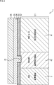
- FIG. 2 is a cross-sectional view showing a configuration example of the solid-state imaging device when an electric field is constantly applied to the insulating film between the N-type substrate and the light shielding metal connected to the ground.
- an example of a back surface solid-state imaging device is shown.
- a wiring layer such as a transistor is disposed in the lower portion of the solid-state imaging device 1 in the drawing.
- an N-type Si substrate 21 is used to electrically and optically connect the pixel region 3 between the N-type pixel region 3 and the N-type peripheral circuit region 41.
- a P-type pixel peripheral region 42 having a certain width is formed so as not to be affected.
- the peripheral circuit region 41 has a light-shielding object, generally a metal (hereinafter referred to as a light-shielding metal) so that light is incident only on the pixel region 3.
- a light-shielding metal a metal
- the structure covered with 25 is applied.
- an insulating film 22 having a fixed charge in the film for example, an insulating film 23 made of SiO2, a metal layer 24, a light shielding metal 25, and an insulating film 26 are formed on the Si substrate 21 in order from the bottom.
- the light shielding metal 25 is made of, for example, tungsten, a compound containing titanium, or aluminum.
- the pixel peripheral area 42 is connected in advance to the ground (GND) so as not to be charged during processing.
- the light shielding metal 25 can be connected to the ground (GND) by forming an opening 31 in the insulating films 22 and 23 on the back surface of the pixel peripheral region 42 to form a contact.
- a positive power supply voltage (for example, 4.5 V) is applied to the peripheral circuit region 41 in order to form a PN junction that is an electrical isolation region in the Si substrate 21 in the N-type substrate. Therefore, an electric field is constantly applied to the insulating film 23 between the positively charged N-type Si substrate 21 and the light shielding metal 25 connected to the ground (GND).
- GND ground
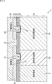
- FIG. 3 is a cross-sectional view illustrating a first configuration example of the solid-state imaging device of the present technology.
- the insulating film 22, the insulating film 23, the metal layer 24, and the insulating film 26 are formed on the Si substrate 21, and the insulating film on the back surface of the pixel peripheral region 42.
- the point that contacts 31 are formed by forming openings 31 in 22 and 23 is the same as the solid-state imaging device 1 of FIG.
- the solid-state imaging device 1 of FIG. 3 instead of the light shielding metal 25, a light shielding metal 52 on the pixel region 3 and a light shielding metal 53 on the peripheral circuit region 41 are formed.
- the solid-state imaging shown in FIG. 2 is that the insulating region 51 is formed between the contact holes and the openings 54 are formed in the insulating films 22 and 23 on the back surface of the peripheral circuit region 41 to form contacts.
- the light shielding metals 52 and 53 are made of, for example, tungsten, a compound containing titanium, or aluminum.
- the light shielding metals 52 and 53 may be made of the same material, or may not be made of the same material.
- the light shielding metal 53 on the peripheral circuit region 41 and the Si substrate 21 are set to the same potential, and no electric field is applied to the insulating films 22 and 23 between the light shielding metal 53 and the Si substrate 21. Like that.
- the light shielding metal 53 on the peripheral circuit region 41 is not connected to the ground (GND), and the openings 54 are formed in the insulating films 22 and 23 on the back surface of the peripheral circuit region 41 to form contacts. Connected to the Si substrate 21. Further, since the light shielding metal 52 on the pixel region 3 is connected to the ground (GND), a divided region (insulating region) 51 where no metal is formed is provided between the light shielding metal 53 on the peripheral circuit region 41. Thus, the light shielding metal 53 on the peripheral circuit region 41 is not short-circuited.
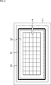
- FIG. 4 is a plan view of the back side of the solid-state imaging device of FIG. In the example of FIG. 4, the cross-sectional view of the solid-state imaging device of FIG.
- the light shielding metal 52 on the pixel region 3 and the light shielding metal 53 on the peripheral circuit region 41 are separated by an insulating region 51.
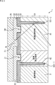
- FIG. 5 is a cross-sectional view illustrating a second configuration example of the solid-state imaging device of the present technology.
- an insulating film 22, an insulating film 23, a metal layer 24, light shielding metals 52 and 53, an insulating region 51, and an insulating film 26 are formed on the Si substrate 21 in order from the bottom.
- a contact is formed by forming an opening 31 in the insulating films 22 and 23 on the back surface of the pixel peripheral region 42, and an opening 54 is formed in the insulating films 22 and 23 on the back surface of the peripheral circuit region 41. The contact is formed in common with the solid-state imaging device 1 of FIG.
- the solid-state imaging device 1 in FIG. 5 is that the light shielding film 101-1 is embedded in the pixel peripheral region 42 and the light shielding film 101-2 is embedded in the peripheral circuit region 41. Is different.
- an insulating region 51 is formed between the light shielding metal 52 on the pixel region 3 and the light shielding metal 53 on the peripheral circuit region 41, and insulation on the back surface of the peripheral circuit region 41.
- the point that the contact is formed by forming the opening 54 in the films 22 and 23 is common to the solid-state imaging device 1 of FIG.
- the light shielding films 101-1 and 101-2 are collectively referred to as the light shielding film 101 when it is not necessary to distinguish between them.
- an electrically insulating region 51 is provided between the light shielding metal 53 connected to the Si substrate of the power supply voltage and the light shielding metal 52 on the pixel region 3 connected to the ground. ing.
- the insulating region 51 that is a region that is not shielded from light is usually provided at a location covered with the light shielding metal. Light enters a device region in the inside or peripheral circuit, and photoelectrically converted electrons may affect the device characteristics.
- One countermeasure is to provide a sufficient distance between the opening and the device region.
- the light shielding material or a film having a refractive index different from that of Si, 101-2 can also be provided. By doing in this way, it can have a structure which refracts light so that incident light may not be totally reflected or enter the device field side.
- the light shielding films 101-1 and 101-2 may be, for example, a compound film containing tungsten, titanium, or a metal film such as aluminum, or a film having a refractive index different from that of Si, for example, an SiO 2 film.
- the light shielding films 101-1 and 101-2 may have a laminated structure of an insulator and a light shielding material.
- the light shielding material at that time may be, for example, a metal film such as a compound containing tungsten or titanium, or aluminum, or may be an SiO 2 film having a property different from that of Si, for example.
- the light shielding films 101 are formed one by one on the left and right sides of the insulating region 51, that is, on the pixel region 3 side and the peripheral circuit region 41 side.
- a plurality may be provided.
- FIG. 6 is a cross-sectional view illustrating a third configuration example of the solid-state imaging device of the present technology.
- an insulating film 22, an insulating film 23, a metal layer 24, light shielding metals 52 and 53, an insulating region 51, and an insulating film 26 are formed on the Si substrate 21 in order from the bottom.
- a contact is formed by forming an opening 31 in the insulating films 22 and 23 on the back surface of the pixel peripheral region 42, and an opening 54 is formed in the insulating films 22 and 23 on the back surface of the peripheral circuit region 41. The contact is formed in common with the solid-state imaging device 1 of FIG.
- FIG. 6 is different from the solid-state imaging device 1 of FIG. 3 in that the Si substrate embedding unit 152 is embedded in the peripheral circuit region 41.
- the solid-state imaging device 1 of FIG. In the example of FIG. 6, a P-type inversion layer 151 is described between the Si substrate 21 and the insulating film 22 for convenience of explanation. This P-type inversion layer 151 is always formed at the back Si interface by the insulating film 22 having a negative fixed charge, and is not particularly described in the examples of FIG. 3 and FIG. Also in the examples of FIGS. 3 and 5, it is always formed at the back Si interface.
- the Si substrate embedded portion 152 is formed by burying an insulating film by dry etching to dig the Si substrate 21 in order to divide the P-type inversion layer 151.
- a part of the P inversion layer 151 formed on the back surface interface where electrons generated from the 4.5 V contact from the 4.5 V side to the ground side flow into the GND side is cut.
- it is effective under high voltage conditions (for example, 4.5 V or more).
- an insulating film 22 which is a film having a fixed charge is formed on the back Si surface, and the back surface Si surface potential is modulated, so that the proposed current characteristics of the pixel due to the charges generated due to the interface state can be obtained.
- the peripheral circuit region 41 and the inside of the pixel 2 are connected by the P-type inversion layer 151 generated by modulating the back surface Si surface.
- the modulation degree of the P-type inversion layer 151 deteriorates due to fluctuations in the fixed charge amount in the film formed on the back surface due to aging of the product, Si surface abnormality, or film quality abnormality of the insulating film, the influence of the interface state There is a possibility that the electric charge due to this increases and flows as a leakage current via the P-type inversion layer 151. If the amount is large, the dark current of the pixel characteristics may be deteriorated due to standby current consumption or light emission of the product.
- FIG. 7 is a cross-sectional view illustrating a fourth configuration example of the solid-state imaging device of the present technology.
- an insulating film 22, an insulating film 23, a metal layer 24, a light shielding metal 25, an insulating region 51, and an insulating film 26 are formed on the Si substrate 21 in order from the bottom.
- the point that the contact is formed by forming the opening 31 in the insulating films 22 and 23 on the back surface of the pixel peripheral region 42 is common to the solid-state imaging device 1 of FIG.
- the solid-state imaging device 1 of FIG. 7 is different from the solid-state imaging device 1 of FIG. 3 in that a Psub substrate is used as the Si substrate 21.
- the solid-state imaging device 1 of FIG. 3 is different from the solid-state imaging device 1 of FIG. 3 in that a Psub substrate is used as the Si substrate 21.
- the peripheral circuit region 41 is a P-type region, like the pixel peripheral region 42 of the Si substrate 21. Therefore, the light shielding metal 25 on the peripheral circuit region 41 and the Si substrate 21 are grounded without applying the structure of the example of FIGS. 3 to 6 (an example in which the Ndub substrate is used).
- the present technology adopts a structure in which the light shielding metal on the back surface and the substrate potential below the same are made the same potential.
- insulation resistance due to, for example, abnormalities in the Si surface of the underlying layer or dust in the insulating film can be achieved in part of the insulating film between the light shielding metal on the peripheral circuit and the Si substrate. Even if a low point occurs, the light shielding metal and the Si substrate are at the same potential, so no current flows between the light shielding metal and the Si substrate, and the connection to the ground (GND) is the pixel in the Si substrate.
- a PN junction is formed between the P-type region in the region and the N-type region in the peripheral circuit region, so that no current exceeding the junction leakage occurs.
- peripheral circuit area there is no electric field between the light shielding metal and the substrate, so there is no longer a short circuit, so the product yield and reliability due to Si surface abnormalities and dust generated in the process up to the formation of the light shielding metal in the back surface process. Risk can be reduced.
- the present technology may be applied to a solid-state imaging device such as a CCD (Charge Coupled Device) solid-state imaging device.
- CCD Charge Coupled Device
- FIG. 8 is a diagram illustrating a usage example in which the above-described solid-state imaging device is used.
- the solid-state imaging device (image sensor) described above can be used in various cases for sensing light such as visible light, infrared light, ultraviolet light, and X-ray as follows.
- Devices for taking images for viewing such as digital cameras and mobile devices with camera functions
- Devices used for traffic such as in-vehicle sensors that capture the back, surroundings, and interiors of vehicles, surveillance cameras that monitor traveling vehicles and roads, and ranging sensors that measure distances between vehicles, etc.
- Equipment used for home appliances such as TVs, refrigerators, air conditioners, etc. to take pictures and operate the equipment according to the gestures ⁇ Endoscopes, equipment that performs blood vessel photography by receiving infrared light, etc.
- Equipment used for medical and health care ⁇ Security equipment such as security surveillance cameras and personal authentication cameras ⁇ Skin measuring instrument for photographing skin and scalp photography Such as a microscope to do beauty Equipment used for sports-Equipment used for sports such as action cameras and wearable cameras for sports applications-Used for agriculture such as cameras for monitoring the condition of fields and crops apparatus
- the present technology is not limited to application to a solid-state imaging device, but can also be applied to an imaging device.
- the imaging apparatus refers to a camera system such as a digital still camera or a digital video camera, or an electronic apparatus having an imaging function such as a mobile phone.
- a module-like form mounted on an electronic device that is, a camera module is used as an imaging device.
- the solid-state imaging device 501 includes a solid-state imaging device (element chip) 501, an optical lens 502, a shutter device 503, a drive circuit 504, and a signal processing circuit 505.
- the solid-state imaging device 501 the solid-state imaging device 1 according to the first embodiment of the present technology described above is provided. Thereby, the product yield and reliability risk of the solid-state imaging device 501 of the electronic device 500 can be reduced.
- the optical lens 502 forms image light (incident light) from the subject on the imaging surface of the solid-state imaging device 501. As a result, signal charges are accumulated in the solid-state imaging device 501 for a certain period.
- the shutter device 503 controls the light irradiation period and the light shielding period for the solid-state imaging device 501.
- the drive circuit 504 supplies a drive signal for controlling the signal transfer operation of the solid-state imaging device 501 and the shutter operation of the shutter device 503.
- the solid-state imaging device 501 performs signal transfer according to a drive signal (timing signal) supplied from the drive circuit 504.
- the signal processing circuit 505 performs various types of signal processing on the signal output from the solid-state imaging device 501.
- the video signal subjected to the signal processing is stored in a storage medium such as a memory or output to a monitor.
- steps describing the series of processes described above are not limited to the processes performed in time series according to the described order, but are not necessarily performed in time series, either in parallel or individually.
- the process to be executed is also included.
- the configuration described as one device (or processing unit) may be divided and configured as a plurality of devices (or processing units).
- the configurations described above as a plurality of devices (or processing units) may be combined into a single device (or processing unit).
- a configuration other than that described above may be added to the configuration of each device (or each processing unit).
- a part of the configuration of a certain device (or processing unit) may be included in the configuration of another device (or other processing unit). . That is, the present technology is not limited to the above-described embodiment, and various modifications can be made without departing from the gist of the present technology.
- this technique can also take the following structures. (1) a pixel region in which pixels are regularly arranged two-dimensionally; Outside the pixel region, a peripheral circuit region in which a circuit that performs signal processing on an image signal from the pixel is disposed; A pixel peripheral region disposed between the pixel region and the peripheral circuit region; A first light shield covering the pixel region and connected to a first potential; A solid-state imaging device comprising: a second light shielding object that covers the peripheral circuit region and is connected to a second potential that is different from the first potential. (2) The solid-state imaging device according to (1), wherein an insulator region surrounding the pixel region is disposed between the first light-blocking object and the second light-blocking object.
- an embedded light shielding film is embedded in an Si substrate in a region between the pixel region and the insulator region.
- the solid-state imaging device according to (6), wherein the film for suppressing incidence of light on the peripheral circuit region side is formed of a film having a refractive index different from that of the Si substrate.
- the solid-state imaging device according to (6), wherein the film for suppressing the incidence of light on the peripheral circuit region side is a light-shielding film.
- the light shielding film has a stacked structure of an insulator and a light shielding material.
- the light shielding film is made of tungsten, a compound containing titanium, or aluminum.
- the solid-state imaging device according to any one of (1) to (10), which is a back surface solid-state imaging device.
- 1 solid-state imaging device 2 pixels, 3 pixel area, 4 vertical drive circuit, 9 vertical signal line, 21 Si substrate, 22 insulating film, 23 insulating film, 24 metal layer, 25 light shielding metal, 26 insulating film, 31 opening, 41 peripheral circuit region, 42 pixel peripheral region, 51 insulating region, 52 light shielding metal, 53 light shielding metal, 54 openings, 101, 101-1, 101-2 light shielding film, 151 P-type inversion layer, 152 Si substrate embedded portion, 500 electronic equipment, 501 solid-state imaging device, 502 optical lens, 503 shutter device, 504 drive circuit, 505 signal processing circuit
Landscapes
- Solid State Image Pick-Up Elements (AREA)
- Transforming Light Signals Into Electric Signals (AREA)
- Physics & Mathematics (AREA)
- Electromagnetism (AREA)
Abstract
Description
1.第1の実施の形態
2.第2の実施の形態(イメージセンサの使用例)
3.第3の実施の形態(電子機器の例)
<固体撮像装置の概略構成例>
図1は、本技術の各実施の形態に適用されるCMOS(Complementary Metal Oxide Semiconductor)固体撮像装置の一例の概略構成例を示している。
図2は、N型基板とグラウンドに接続された遮光メタルの間の絶縁膜に定常的に電界がかかる場合の固体撮像装置の構成例を示す断面図である。図2の例においては、裏面固体撮像装置の例が示されている。また、図2の例においては、記載されていないが、実際には、固体撮像装置1における、図中下部にトランジスタなどの配線層が配置されている。
図3は、本技術の固体撮像装置の第1の構成例を示す断面図である。
図5は、本技術の固体撮像装置の第2の構成例を示す断面図である。
図6は、本技術の固体撮像装置の第3の構成例を示す断面図である。
図7は、本技術の固体撮像装置の第4の構成例を示す断面図である。
図8は、上述の固体撮像装置を使用する使用例を示す図である。
・自動停止等の安全運転や、運転者の状態の認識等のために、自動車の前方や後方、周囲、車内等を撮影する車載用センサ、走行車両や道路を監視する監視カメラ、車両間等の測距を行う測距センサ等の、交通の用に供される装置
・ユーザのジェスチャを撮影して、そのジェスチャに従った機器操作を行うために、TVや、冷蔵庫、エアーコンディショナ等の家電に供される装置
・内視鏡や、赤外光の受光による血管撮影を行う装置等の、医療やヘルスケアの用に供される装置
・防犯用途の監視カメラや、人物認証用途のカメラ等の、セキュリティの用に供される装置
・肌を撮影する肌測定器や、頭皮を撮影するマイクロスコープ等の、美容の用に供される装置
・スポーツ用途等向けのアクションカメラやウェアラブルカメラ等の、スポーツの用に供される装置
・畑や作物の状態を監視するためのカメラ等の、農業の用に供される装置
<電子機器の構成例>
(1) 画素が規則的に2次元的に配列された画素領域と、
前記画素領域の外側において、前記画素からの画像信号に対して信号処理を行う回路が配置される周辺回路領域と、
前記画素領域と前記周辺回路領域の間に配置される画素周辺領域と、
前記画素領域を覆い、第1の電位に接続されている第1の遮光物と、
前記周辺回路領域を覆い、前記第1の電位とは異なる電位である第2の電位に接続されている第2の遮光物と
を備える固体撮像装置。
(2) 前記第1の遮光物と前記第2の遮光物との間において、前記画素領域を囲む絶縁体領域が配置されている
前記(1)に記載の固体撮像装置。
(3) 前記第1の遮光物および第2遮光物のうち少なくとも1つは、タングステン、チタンを含む化合物、またはアルミで構成されている
前記(1)または(2)に記載の固体撮像装置。
(4) 前記絶縁体領域内におけるSi基板の表面を掘り込んで形成された埋め込み部が設けられている
前記(1)乃至(3)のいずれかに記載の固体撮像装置。
(5) 前記埋め込み部は、絶縁物が埋め込まれて形成されている
前記(4)に記載の固体撮像装置。
(6) 前記画素領域と前記絶縁体領域内の間にある領域におけるSi基板の内部に、埋め込み遮光膜が埋め込まれている
前記(1)乃至(4)のいずれかに記載の固体撮像装置。
(7) 前記周辺回路領域側への光の入射を抑制するための膜は、Si基板と屈折率が異なる膜で構成されている
前記(6)に記載の固体撮像装置。
(8) 前記周辺回路領域側への光の入射を抑制するための膜は、遮光膜で構成されている
前記(6)に記載の固体撮像装置。
(9) 前記遮光膜は、絶縁物と遮光物の積層構造である
前記(8)に記載の固体撮像装置。
(10) 前記遮光膜は、タングステン、チタンを含む化合物、またはアルミで構成されている
前記(8)に記載の固体撮像装置。
(11) 裏面固体撮像装置である
前記(1)乃至(10)のいずれかに記載の固体撮像装置。
(12) 規則的に2次元的に配列された画素と、
垂直加算を行う際に、垂直加算対象の画素のうちの一方が、撮像以外の機能を有する特殊画素である場合、前記垂直加算対象の画素のどちらかのみを出力する垂直加算回路と
を備える固体撮像装置と、
前記固体撮像装置から出力される出力信号を処理する信号処理回路と、
入射光を前記固体撮像装置に入射する光学系と
を有する電子機器。
Claims (12)
- 画素が規則的に2次元的に配列された画素領域と、
前記画素領域の外側において、前記画素からの画像信号に対して信号処理を行う回路が配置される周辺回路領域と、
前記画素領域と前記周辺回路領域の間に配置される画素周辺領域と、
前記画素領域を覆い、第1の電位に接続されている第1の遮光物と、
前記周辺回路領域を覆い、前記第1の電位とは異なる電位である第2の電位に接続されている第2の遮光物と
を備える固体撮像装置。 - 前記第1の遮光物と前記第2の遮光物との間において、前記画素領域を囲む絶縁体領域が配置されている
請求項1に記載の固体撮像装置。 - 前記第1の遮光物および第2遮光物のうち少なくとも1つは、タングステン、チタンを含む化合物、またはアルミで構成されている
請求項1に記載の固体撮像装置。 - 前記絶縁体領域内におけるSi基板の表面を掘り込んで形成された埋め込み部が設けられている
請求項2に記載の固体撮像装置。 - 前記埋め込み部は、絶縁物が埋め込まれて形成されている
請求項4に記載の固体撮像装置。 - 前記画素領域と前記絶縁体領域内の間にある領域におけるSi基板の内部に、前記周辺回路領域側への光の入射を抑制するための膜が埋め込まれている
請求項2に記載の固体撮像装置。 - 前記周辺回路領域側への光の入射を抑制するための膜は、Si基板と屈折率が異なる膜で構成されている
請求項6に記載の固体撮像装置。 - 前記周辺回路領域側への光の入射を抑制するための膜は、遮光膜で構成されている
請求項6に記載の固体撮像装置。 - 前記遮光膜は、絶縁物と遮光物の積層構造である
請求項8に記載の固体撮像装置。 - 前記遮光膜は、タングステン、チタンを含む化合物、またはアルミで構成されている
請求項8に記載の固体撮像装置。 - 裏面固体撮像装置である
請求項1に記載の固体撮像装置。 - 画素が規則的に2次元的に配列された画素領域と、
前記画素領域の外側において、前記画素からの画像信号に対して信号処理を行う回路が配置される周辺回路領域と、
前記画素領域と前記周辺回路領域の間に配置される画素周辺領域と、
前記画素領域を覆い、第1の電位に接続されている第1の遮光物と、
前記周辺回路領域を覆い、前記第1の電位とは異なる電位である第2の電位に接続されている第2の遮光物と
を備える固体撮像装置と、
前記固体撮像装置から出力される出力信号を処理する信号処理回路と、
入射光を前記固体撮像装置に入射する光学系と
を有する電子機器。
Priority Applications (2)
| Application Number | Priority Date | Filing Date | Title |
|---|---|---|---|
| US15/753,495 US10453885B2 (en) | 2015-09-09 | 2016-08-26 | Solid-state imaging apparatus and electronic device |
| JP2017539108A JP6776247B2 (ja) | 2015-09-09 | 2016-08-26 | 固体撮像装置および電子機器 |
Applications Claiming Priority (2)
| Application Number | Priority Date | Filing Date | Title |
|---|---|---|---|
| JP2015177293 | 2015-09-09 | ||
| JP2015-177293 | 2015-09-09 |
Publications (1)
| Publication Number | Publication Date |
|---|---|
| WO2017043330A1 true WO2017043330A1 (ja) | 2017-03-16 |
Family
ID=58239481
Family Applications (1)
| Application Number | Title | Priority Date | Filing Date |
|---|---|---|---|
| PCT/JP2016/074915 Ceased WO2017043330A1 (ja) | 2015-09-09 | 2016-08-26 | 固体撮像装置および電子機器 |
Country Status (3)
| Country | Link |
|---|---|
| US (1) | US10453885B2 (ja) |
| JP (1) | JP6776247B2 (ja) |
| WO (1) | WO2017043330A1 (ja) |
Families Citing this family (2)
| Publication number | Priority date | Publication date | Assignee | Title |
|---|---|---|---|---|
| TW201101476A (en) * | 2005-06-02 | 2011-01-01 | Sony Corp | Semiconductor image sensor module and method of manufacturing the same |
| JP7346072B2 (ja) * | 2019-04-26 | 2023-09-19 | キヤノン株式会社 | 光電変換装置、撮像システム、および、移動体 |
Citations (5)
| Publication number | Priority date | Publication date | Assignee | Title |
|---|---|---|---|---|
| JP2007165650A (ja) * | 2005-12-14 | 2007-06-28 | Sony Corp | 固体撮像装置 |
| JP2009099626A (ja) * | 2007-10-12 | 2009-05-07 | Toshiba Corp | 撮像装置 |
| JP2012064709A (ja) * | 2010-09-15 | 2012-03-29 | Sony Corp | 固体撮像装置及び電子機器 |
| JP2014192348A (ja) * | 2013-03-27 | 2014-10-06 | Sony Corp | 固体撮像装置およびその製造方法、並びに電子機器 |
| JP2015032640A (ja) * | 2013-07-31 | 2015-02-16 | 株式会社東芝 | 固体撮像装置および固体撮像装置の製造方法 |
Family Cites Families (4)
| Publication number | Priority date | Publication date | Assignee | Title |
|---|---|---|---|---|
| JP2007299840A (ja) * | 2006-04-28 | 2007-11-15 | Fujifilm Corp | Ccd型固体撮像素子及びその製造方法 |
| JP5735318B2 (ja) | 2011-03-23 | 2015-06-17 | シャープ株式会社 | 固体撮像素子および電子情報機器 |
| JP2012238648A (ja) * | 2011-05-10 | 2012-12-06 | Sony Corp | 固体撮像装置及び電子機器 |
| JP5725123B2 (ja) | 2013-10-04 | 2015-05-27 | ソニー株式会社 | 固体撮像装置及び電子機器 |
-
2016
- 2016-08-26 US US15/753,495 patent/US10453885B2/en active Active
- 2016-08-26 WO PCT/JP2016/074915 patent/WO2017043330A1/ja not_active Ceased
- 2016-08-26 JP JP2017539108A patent/JP6776247B2/ja not_active Expired - Fee Related
Patent Citations (5)
| Publication number | Priority date | Publication date | Assignee | Title |
|---|---|---|---|---|
| JP2007165650A (ja) * | 2005-12-14 | 2007-06-28 | Sony Corp | 固体撮像装置 |
| JP2009099626A (ja) * | 2007-10-12 | 2009-05-07 | Toshiba Corp | 撮像装置 |
| JP2012064709A (ja) * | 2010-09-15 | 2012-03-29 | Sony Corp | 固体撮像装置及び電子機器 |
| JP2014192348A (ja) * | 2013-03-27 | 2014-10-06 | Sony Corp | 固体撮像装置およびその製造方法、並びに電子機器 |
| JP2015032640A (ja) * | 2013-07-31 | 2015-02-16 | 株式会社東芝 | 固体撮像装置および固体撮像装置の製造方法 |
Also Published As
| Publication number | Publication date |
|---|---|
| US20180247966A1 (en) | 2018-08-30 |
| JPWO2017043330A1 (ja) | 2018-06-28 |
| US10453885B2 (en) | 2019-10-22 |
| JP6776247B2 (ja) | 2020-10-28 |
Similar Documents
| Publication | Publication Date | Title |
|---|---|---|
| US11322534B2 (en) | Solid-state imaging device and electronic apparatus | |
| JP7472952B2 (ja) | 撮像装置 | |
| US11610924B2 (en) | Solid-state imaging device capable of inhibiting peeling of fixed charge film, method of manufacturing the same, and electronic device | |
| US10236311B2 (en) | Solid-state imaging element and electronic device to improve quality of an image | |
| US10805562B2 (en) | Imaging device, manufacturing method, semiconductor device, and electronic device | |
| US20170358614A1 (en) | Solid-state imaging device and electronic apparatus | |
| CN108352395B (zh) | 固态摄像装置和电子设备 | |
| US11218656B2 (en) | Solid-state imaging device and electronic apparatus | |
| JP7279768B2 (ja) | 固体撮像素子、および電子装置 | |
| CN107408566B (zh) | 固态成像设备和电子装置 | |
| TWI709235B (zh) | 固體攝像元件、其製造方法及電子機器 | |
| US20240014343A1 (en) | Solid-state imaging element, imaging device, and electronic device | |
| JPWO2017159362A1 (ja) | 固体撮像素子およびその製造方法、並びに電子機器 | |
| US20200185433A1 (en) | Semiconductor device, solid-state image pickup element, imaging device, and electronic apparatus | |
| JP6776247B2 (ja) | 固体撮像装置および電子機器 | |
| US20240089619A1 (en) | Light detection device and electronic apparatus | |
| US20180083059A1 (en) | Solid-state image capture element and electronic device |
Legal Events
| Date | Code | Title | Description |
|---|---|---|---|
| 121 | Ep: the epo has been informed by wipo that ep was designated in this application |
Ref document number: 16844193 Country of ref document: EP Kind code of ref document: A1 |
|
| ENP | Entry into the national phase |
Ref document number: 2017539108 Country of ref document: JP Kind code of ref document: A |
|
| WWE | Wipo information: entry into national phase |
Ref document number: 15753495 Country of ref document: US |
|
| NENP | Non-entry into the national phase |
Ref country code: DE |
|
| 122 | Ep: pct application non-entry in european phase |
Ref document number: 16844193 Country of ref document: EP Kind code of ref document: A1 |