WO2017038256A1 - 撮像素子、積層型撮像素子及び固体撮像装置 - Google Patents
撮像素子、積層型撮像素子及び固体撮像装置 Download PDFInfo
- Publication number
- WO2017038256A1 WO2017038256A1 PCT/JP2016/070637 JP2016070637W WO2017038256A1 WO 2017038256 A1 WO2017038256 A1 WO 2017038256A1 JP 2016070637 W JP2016070637 W JP 2016070637W WO 2017038256 A1 WO2017038256 A1 WO 2017038256A1
- Authority
- WO
- WIPO (PCT)
- Prior art keywords
- group
- electrode
- photoelectric conversion
- imaging device
- structural formula
- Prior art date
- Legal status (The legal status is an assumption and is not a legal conclusion. Google has not performed a legal analysis and makes no representation as to the accuracy of the status listed.)
- Ceased
Links
Images




Classifications
-
- H—ELECTRICITY
- H10—SEMICONDUCTOR DEVICES; ELECTRIC SOLID-STATE DEVICES NOT OTHERWISE PROVIDED FOR
- H10F—INORGANIC SEMICONDUCTOR DEVICES SENSITIVE TO INFRARED RADIATION, LIGHT, ELECTROMAGNETIC RADIATION OF SHORTER WAVELENGTH OR CORPUSCULAR RADIATION
- H10F39/00—Integrated devices, or assemblies of multiple devices, comprising at least one element covered by group H10F30/00, e.g. radiation detectors comprising photodiode arrays
- H10F39/10—Integrated devices
- H10F39/12—Image sensors
-
- H—ELECTRICITY
- H10—SEMICONDUCTOR DEVICES; ELECTRIC SOLID-STATE DEVICES NOT OTHERWISE PROVIDED FOR
- H10K—ORGANIC ELECTRIC SOLID-STATE DEVICES
- H10K30/00—Organic devices sensitive to infrared radiation, light, electromagnetic radiation of shorter wavelength or corpuscular radiation
-
- Y—GENERAL TAGGING OF NEW TECHNOLOGICAL DEVELOPMENTS; GENERAL TAGGING OF CROSS-SECTIONAL TECHNOLOGIES SPANNING OVER SEVERAL SECTIONS OF THE IPC; TECHNICAL SUBJECTS COVERED BY FORMER USPC CROSS-REFERENCE ART COLLECTIONS [XRACs] AND DIGESTS
- Y02—TECHNOLOGIES OR APPLICATIONS FOR MITIGATION OR ADAPTATION AGAINST CLIMATE CHANGE
- Y02E—REDUCTION OF GREENHOUSE GAS [GHG] EMISSIONS, RELATED TO ENERGY GENERATION, TRANSMISSION OR DISTRIBUTION
- Y02E10/00—Energy generation through renewable energy sources
- Y02E10/50—Photovoltaic [PV] energy
- Y02E10/549—Organic PV cells
Definitions
- the present disclosure relates to an imaging device, a stacked imaging device, and a solid-state imaging device.
- An image sensor using an organic semiconductor material for the photoelectric conversion layer can photoelectrically convert a specific color (wavelength band). And since it has such a feature, when it is used as an image sensor in a solid-state imaging device, sub-pixels are composed of a combination of an on-chip color filter (OCCF) and an image sensor, and the sub-pixels are two-dimensionally arranged. It is possible to obtain a structure in which subpixels are stacked (stacked image sensor), which is impossible with a conventional solid-state image sensor. Further, since no demosaic processing is required, there is an advantage that no false color is generated.
- OCCF on-chip color filter
- the image sensor is required to have a high external quantum efficiency (EQE) and a low dark current (having a high S / N ratio).
- EQE external quantum efficiency
- dark current having a high S / N ratio
- DIP diindenoperylene
- DIP is a material with high hole mobility.
- the photoelectric conversion layer of the image sensor is made of DIP, excellent spectral characteristics cannot be obtained. That is, for example, the photoelectric conversion layer does not show a high absorption peak for light having a wavelength of 450 nm to 600 nm, and there is a problem that the amount of light absorption is small (see FIG. 5).
- an object of the present disclosure is to provide an imaging device including a photoelectric conversion layer having characteristics such as high external quantum efficiency and low dark current, and exhibiting a high absorption peak with respect to light having a wavelength of 450 nm to 600 nm, and the imaging device It is an object of the present invention to provide a multilayer imaging device having the above, a solid-state imaging device including the imaging device or the multilayer imaging device.
- An image sensor for achieving the above-described object, Comprising a first electrode, a second electrode, and a photoelectric conversion layer disposed between the first electrode and the second electrode;
- the photoelectric conversion layer A diindenoperylene derivative having a maximum absorption peak in a wavelength range of 450 nm to 600 nm and having the following structural formula (1); and Organic semiconductor material that absorbs green color, Consisting of By applying a voltage to the first electrode and the second electrode, a current generated in the photoelectric conversion layer by light irradiation is extracted to the outside through the first electrode and the second electrode.
- X 1 to X 8 are each independently an alkyl group that may have a substituent, a heteroalkyl group, an aryl group that may have a substituent, a heteroaryl group, a carbocyclic compound, or a heterocyclic compound. Become.
- the image sensor according to the second aspect of the present disclosure for achieving the above-described object, Comprising a first electrode, a second electrode, and a photoelectric conversion layer disposed between the first electrode and the second electrode;
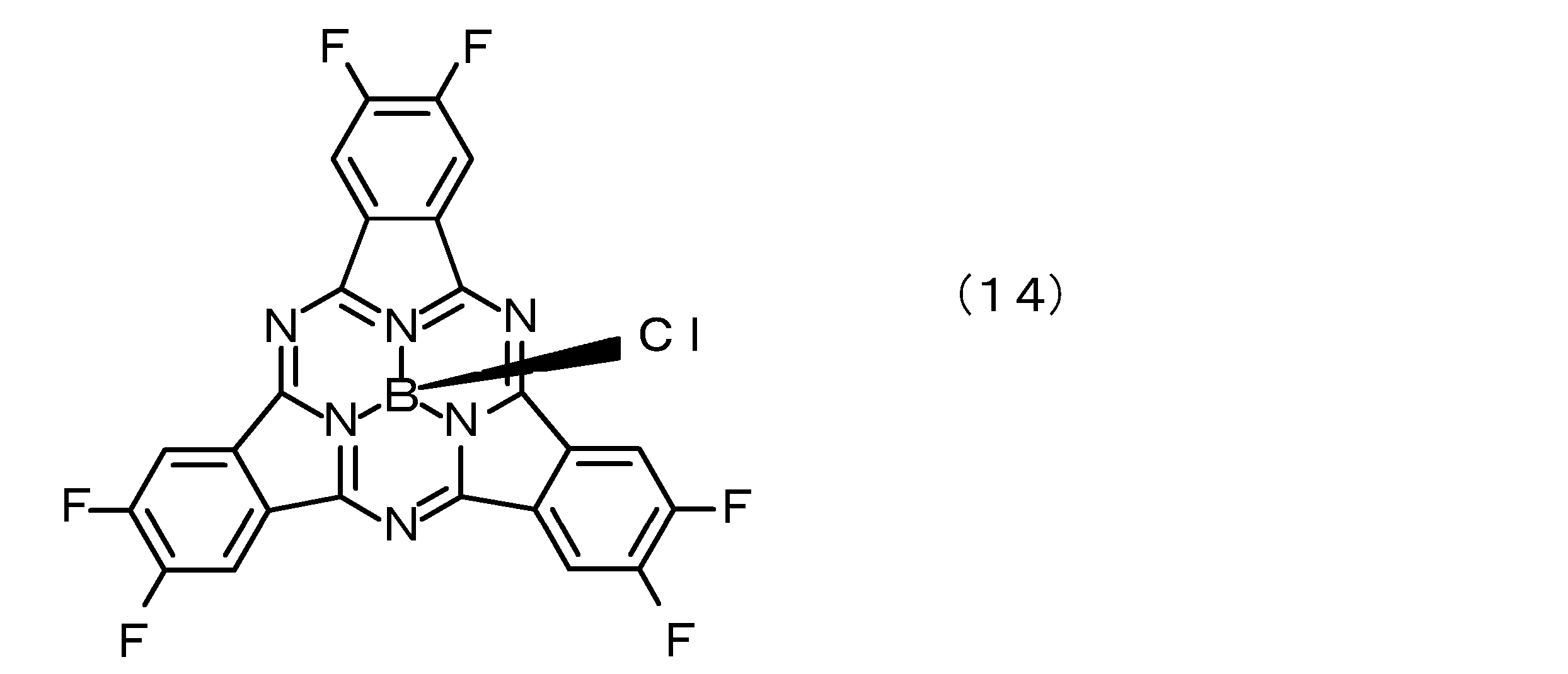
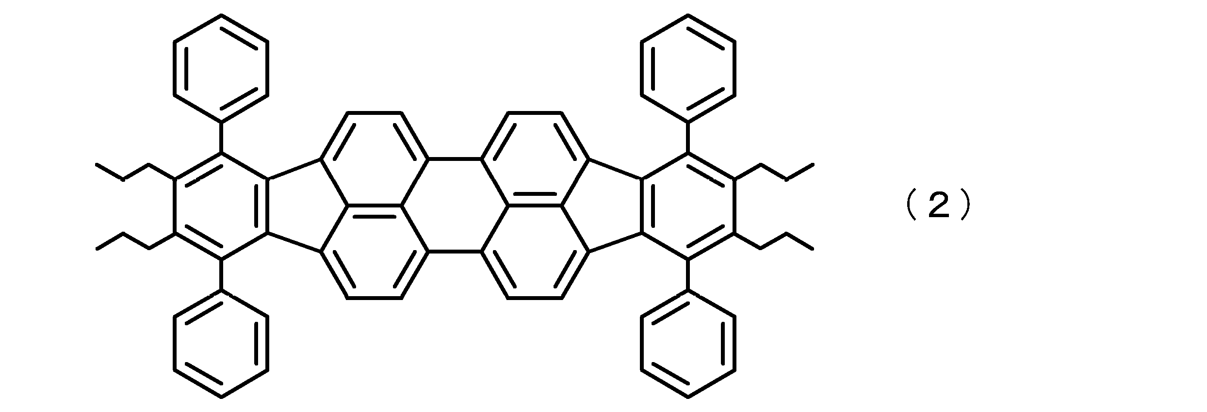
- the photoelectric conversion layer comprises a diindenoperylene derivative having the following structural formula (2), abbreviated as “P4-Ph4-DIP”, and a structural formula (14), abbreviated as “F6SubPc-Cl”. It comprises a bulk hetero layer made of an n-type organic semiconductor material.
- the multilayer image sensor of the present disclosure is formed by stacking one image sensor according to the first to second aspects of the present disclosure.
- the solid-state imaging device according to the first aspect of the present disclosure for achieving the above object includes a plurality of imaging elements according to the first to second aspects of the present disclosure.
- the solid-state imaging device according to the second aspect of the present disclosure for achieving the above object includes a plurality of stacked imaging elements of the present disclosure.
- the imaging element according to the first aspect to the second aspect of the present disclosure the imaging element constituting the stacked imaging element of the present disclosure, and the solid-state imaging device according to the first aspect to the second aspect of the present disclosure are configured.
- the photoelectric conversion layer is composed of a diindenoperylene (DIP) derivative.
- DIP diindenoperylene
- the photoelectric conversion layer exhibits a high absorption peak for light having a wavelength of 450 nm to 600 nm. Therefore, a solid-state imaging device having excellent characteristics can be provided. Note that the effects described in the present specification are merely examples and are not limited, and may have additional effects.
- FIG. 1 is a schematic cross-sectional view of the image sensor according to the first embodiment.
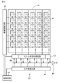
- FIG. 2 is a conceptual diagram of the solid-state imaging device according to the second embodiment.
- FIG. 3 is a diagram showing an outline of a synthesis scheme of a diindenoperylene derivative having the structural formula (2).
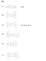
- FIG. 4 is a diagram showing six types of structures used when performing an ultraviolet-visible absorption spectrum (UV-VIS) calculation by a time-dependent density functional method (TD-DFT).
- FIG. 5 is a graph showing the results of spectroscopic measurement of the diindenoperylene thin film having the structural formula (2) and the diindenoperylene thin film using an ultraviolet-visible spectrophotometer.
- FIG. 6B are graphs showing the results of evaluating the spectral characteristics in the image sensors of Example 1A and Example 1B, respectively.
- FIG. 7 is a graph showing the results of evaluating the spectral characteristics in the image sensor of Example 1C.
- 8A and 8B are conceptual diagrams of the multilayer image sensor of Example 2.
- Example 1 the image sensor according to the first to second aspects of the present disclosure and the solid-state imaging device according to the first aspect of the present disclosure
- Example 2 stacked imaging device according to the present disclosure and solid-state imaging device according to the second aspect of the present disclosure
- the imaging device according to the first aspect of the present disclosure, the imaging device according to the first aspect of the present disclosure that constitutes the stacked imaging device of the present disclosure, and the book that constitutes the solid-state imaging device according to the first aspect of the present disclosure
- the LUMO value of the n-type organic semiconductor material is It is preferably 0.2 eV or more lower than the LUMO value of the diindenoperylene derivative having the structural formula (1).
- the photoelectric conversion layer can be configured to have a bulk heterostructure.
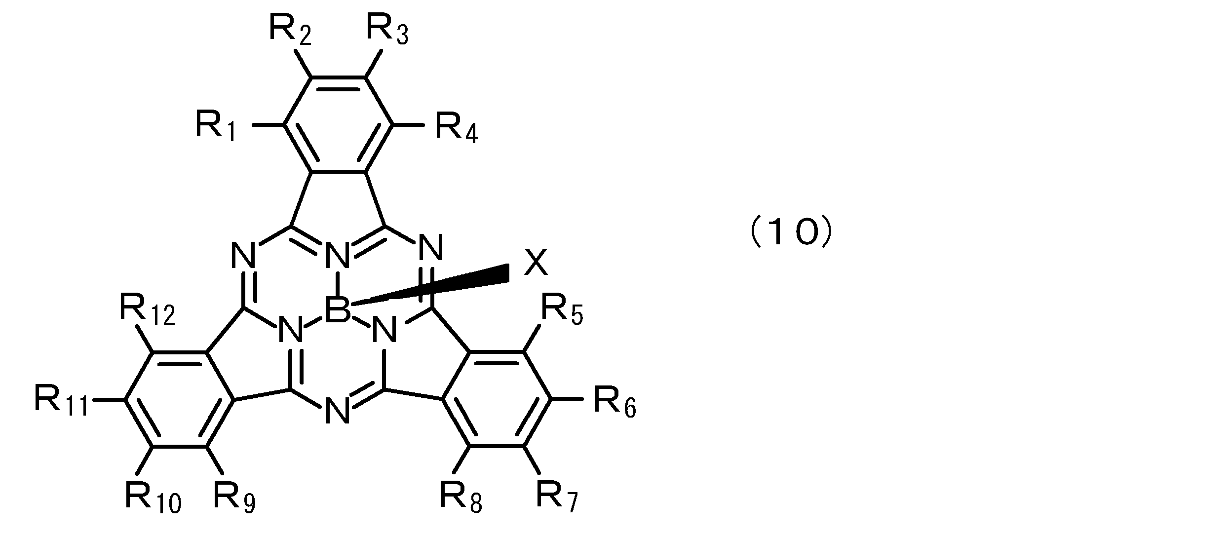
- the n-type organic semiconductor material may be configured by the following structural formula (10).
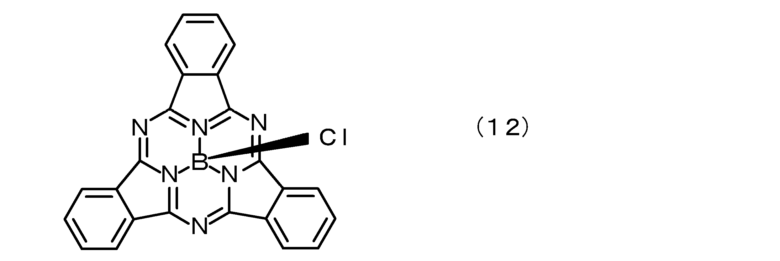
- the n-type organic semiconductor material specifically includes the following structural formula (11), more specifically, the following structural formula (12) abbreviated as “SubPc—Cl”.
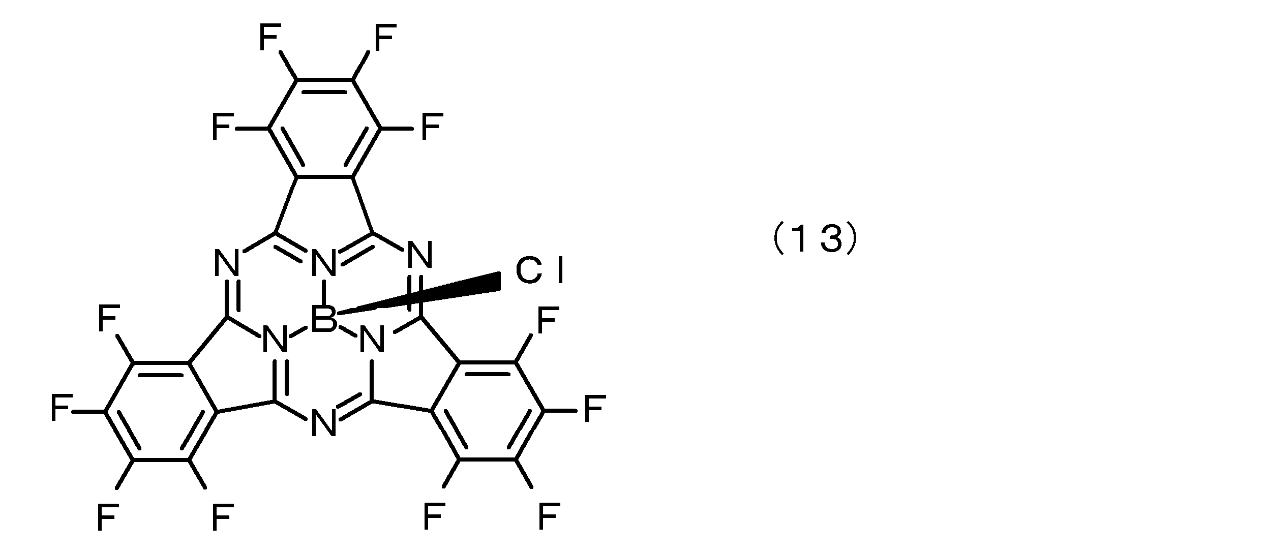
- the n-type organic semiconductor material may be in the form of the following structural formula (13) abbreviated as “F12SubPc-Cl”, or alternatively it may be abbreviated as “F6SubPc-Cl” It can be made into the form which consists of Structural formula (14).
- X and R 1 to R 12 are each independently a hydrogen atom; a halogen atom containing chlorine and fluorine; or a linear, branched or cyclic alkyl group or phenyl group; a linear or condensed aromatic A ring, a partial fluoroalkyl group, a perfluoroalkyl group, a silylalkyl group, a silylalkoxy group, an arylsilyl group, a thioalkyl group, a thioaryl group, an arylsulfonyl group, an alkylsulfonyl group, an amino group, an alkylamino group, an arylamino group, a hydroxy An alkoxy group; an acylamino group; an acyloxy group; a carboxy group; a carboxamide group; a carboalkoxy group; an acyl group; a sulfonyl group; a cyano group; and
- diindenoperylene derivatives having the structural formula (1) or the structural formula (2) Is called a p-type semiconductor material.
- Organic semiconductors are often classified as p-type and n-type, and p-type means that holes are easily transported, and n-type means that electrons are easily transported. It is not limited to the interpretation of having holes or electrons as majority carriers for thermal excitation as in a semiconductor.
- the photoelectric conversion layer may further contain a p-type semiconductor material and / or an n-type semiconductor material.
- the first electrode and the second electrode can be made of a transparent conductive material.
- one of the first electrode and the second electrode can be made of a transparent conductive material, and the other can be made of a metal material.
- the light incident side electrode is made of a transparent conductive material.
- a transparent electrode Such an electrode is called a “transparent electrode”.
- indium-tin oxide including ITO, Sn-doped In 2 O 3 , crystalline ITO and amorphous ITO
- IFO F-doped In 2 O 3
- Tin oxide SnO 2
- ATO Sb-doped SnO 2
- FTO F-doped SnO 2
- zinc oxide including Al-doped ZnO, B-doped ZnO, Ga-doped ZnO
- indium oxide-oxidation examples thereof include zinc (IZO), titanium oxide (TiO 2 ), spinel oxide, and oxide having a YbFe 2 O 4 structure.
- the conductive material constituting the first electrode or the second electrode when the first electrode or the second electrode functions as a cathode electrode (cathode), that is, as the electrode for extracting holes.
- gold (Au), silver (Ag), chromium (Cr), nickel (Ni), palladium (Pd), platinum (Pt), iron (Fe), iridium (Ir), germanium (Ge), osmium (Os), rhenium (Re), and tellurium (Te) can be exemplified.
- an alkali metal for example, Li, Na, K, etc.
- a fluoride or oxide thereof an alkaline earth metal (for example, Mg, Ca, etc.) and a fluoride or oxide thereof
- alkaline earth metal for example, Mg, Ca, etc.
- alkali metal for example, Li, Na, K, etc.
- alkaline earth metal for example, Mg, Ca, etc.
- alkali metal for example, Li, Na, K, etc.
- an alkaline earth metal for example, Mg, Ca, etc.
- examples include aluminum (Al), zinc (Zn), tin (Sn), thallium (Tl), sodium-potassium alloy, aluminum-lithium alloy, magnesium-silver alloy, rare earth metals such as indium and ytterbium, or alloys thereof. be able to.
- platinum Pt
- gold Au
- palladium Pd
- chromium Cr
- nickel Ni
- aluminum Al
- silver Ag
- Tantalum Ta
- tungsten W
- copper Cu
- titanium Ti
- indium In
- tin Sn
- iron Fe
- cobalt Co
- molybdenum Mo
- Alloys containing these metal elements conductive particles made of these metals, conductive particles of alloys containing these metals, polysilicon containing impurities, carbon-based materials, oxide semiconductors, carbon nano tubes,
- An electroconductive substance such as graphene can be given, and a stacked structure of layers containing these elements can also be used.
- examples of the material constituting the first electrode and the second electrode include a material (conductive polymer) such as poly (3,4-ethylenedioxythiophene) / polystyrene sulfonic acid [PEDOT / PSS].
- these conductive materials may be mixed with a binder (polymer) to form a paste or ink, which may be used as an electrode.
- the method of forming the first electrode and the second electrode depends on the materials constituting them, but various PVD methods; various CVD methods including MOCVD method; various coating methods; dipping method; pyrosol method; organometallic compound A pyrolysis method; a lift-off method; a sol-gel method; an electrodeposition method; a shadow mask method; a plating method such as an electrolytic plating method, an electroless plating method, or a combination thereof; and one of spray methods; A combination with a patterning technique can be given as necessary.
- the surface of the first electrode or the second electrode can be treated with oxygen plasma, argon plasma, nitrogen plasma, ozone, or the like.
- Various vacuum deposition methods such as an electron beam heating method, an electron beam deposition method, a resistance heating method, a flash deposition method, a reactive deposition method, etc .; plasma deposition method; bipolar sputtering method, direct current sputtering method, direct current magnetron sputtering method Various sputtering methods such as high frequency sputtering method, magnetron sputtering method, ion beam sputtering method, bias sputtering method; DC (direct current) method, RF method, multi-cathode method, activation reaction method, electric field deposition method, high frequency ion plating And various ion plating methods such as a reactive ion plating method.
- the application method includes spin coating method; dipping method; casting method; various printing methods such as screen printing method, ink jet printing method, offset printing method and gravure printing method; stamp method; spray method; air doctor coater method, Blade coater method, rod coater method, knife coater method, squeeze coater method, reverse roll coater method, transfer roll coater method, gravure coater method, kiss coater method, cast coater method, spray coater method, slit orifice coater method, calendar coater method, etc.
- various coating methods can be exemplified.
- a form in which the first buffer layer / photoelectric conversion layer / second buffer layer is formed between the first electrode and the second electrode, photoelectric conversion layer / second buffer It can be set as the form in which the layer is formed.
- the first buffer layer / n-type organic material layer / photoelectric conversion layer / p-type organic material layer / second buffer are provided between the first electrode and the second electrode. It can be set as the form in which the layer is formed.
- a hole blocking layer / photoelectric conversion layer / electron blocking layer may be formed between the first electrode and the second electrode.
- examples of the inorganic material include alkali metals such as lithium (Li), sodium (Na), and potassium (K) and fluorides and oxides thereof, magnesium (Mg), calcium ( Mention may be made of alkaline earth metals such as Ca) and their fluorides and oxides.
- the first electrode made of a transparent conductive material is formed on a transparent substrate,
- the photoelectric conversion layer is formed on the first electrode,
- the 2nd electrode can be set as the structure currently formed on the photoelectric converting layer.
- the first electrode is formed on the substrate,
- the photoelectric conversion layer is formed on the first electrode,
- the second electrode made of a transparent conductive material can be configured to be formed on the photoelectric conversion layer.
- the 1st electrode and the 2nd electrode are separated, the form by which the 2nd electrode is provided above the 1st electrode can be mentioned as such a separation state.
- the photoelectric conversion layer is preferably formed (film formation) based on a co-evaporation method, but is not limited to such a method.
- the thickness of the photoelectric conversion layer is not limited, but, for example, 1 ⁇ 10 ⁇ 8 m to 5 ⁇ 10 ⁇ 7 m, preferably 2.5 ⁇ 10 ⁇ 8 m to 3 ⁇ 10 ⁇ 7 m Preferably, it is 2.5 ⁇ 10 ⁇ 8 m to 2 ⁇ 10 ⁇ 7 m, more preferably 1 ⁇ 10 ⁇ 7 m to 1.8 ⁇ 10 ⁇ 7 m.
- polymethyl methacrylate polymethyl methacrylate
- PMMA polyvinyl alcohol
- PVP polyvinyl phenol
- PES polyethersulfone
- PC polycarbonate
- PET polyethylene terephthalate
- PEN polyethylene naphthalate
- an organic polymer having the form of a polymer material such as a flexible plastic film or plastic sheet composed of a polymer material, or a plastic substrate
- various glass substrates various glass substrates having an insulating film formed on the surface, quartz substrates, quartz substrates having an insulating film formed on the surface, silicon substrates having an insulating film formed on the surface, stainless steel, etc.
- metal substrates made of various alloys and various metals.
- a silicon oxide-based material for example, SiO x or spin-on glass (SOG)
- SiN Y silicon nitride
- SiON silicon oxynitride
- Al 2 O 3 aluminum oxide
- metal oxide or Mention may be made of metal salts.
- a conductive substrate (a substrate made of a metal such as gold or aluminum or a substrate made of highly oriented graphite) having these insulating films formed on the surface can also be used.
- the surface of the substrate is desirably smooth, but may have a roughness that does not adversely affect the characteristics of the photoelectric conversion layer.
- a silanol derivative is formed on the surface of the substrate by a silane coupling method, a thin film made of a thiol derivative, a carboxylic acid derivative, a phosphoric acid derivative, or the like is formed by a SAM method, or an insulating metal salt or metal is formed by a CVD method or the like.
- a transparent substrate refers to a substrate made of a material that does not excessively absorb light incident on the photoelectric conversion layer through the substrate.
- a material constituting the coating layer not only an inorganic insulating material exemplified by a metal oxide high dielectric insulating film such as a silicon oxide material; silicon nitride (SiN Y ); aluminum oxide (Al 2 O 3 ), Polymethylmethacrylate (PMMA); Polyvinylphenol (PVP); Polyvinyl alcohol (PVA); Polyimide; Polycarbonate (PC); Polyethylene terephthalate (PET); Polystyrene; N-2 (aminoethyl) 3-aminopropyltrimethoxysilane (AEAPTMS) ), Silanol derivatives (silane coupling agents) such as 3-mercaptopropyltrimethoxysilane (MPTMS) and octadecyltrichlorosilane (OTS); a functional group capable of binding to the electrode at one end,
- a metal oxide high dielectric insulating film such as a silicon oxide material; silicon nitride (
- organic insulating material exemplified by hydrogen compound (organic polymers) may also be used a combination thereof.
- Silicon oxide-based materials include silicon oxide (SiO x ), BPSG, PSG, BSG, AsSG, PbSG, silicon oxynitride (SiON), SOG (spin-on-glass), low dielectric constant materials (for example, polyaryl ether, cyclohexane) Examples thereof include perfluorocarbon polymer and benzocyclobutene, cyclic fluororesin, polytetrafluoroethylene, fluorinated aryl ether, fluorinated polyimide, amorphous carbon, and organic SOG).
- the solid-state imaging device can be a front-side irradiation type or a back-side irradiation type, and a single-plate color solid-state imaging device can be configured.
- a method of forming a pattern based on a PLD method pulse laser deposition method
- the image sensor may be provided with an on-chip micro lens and a light shielding layer as necessary, and a drive circuit and wiring for driving the image sensor are provided. If necessary, a shutter for controlling the incidence of light on the imaging device may be provided, or an optical cut filter may be provided depending on the purpose of the solid-state imaging device.
- the array of imaging elements is Bayer array, interline array, G stripe RB checkered array, G stripe RB complete checkered pattern. Examples include an array, a checkered complementary color array, a stripe array, an oblique stripe array, a primary color difference array, a field color difference sequential array, a frame color difference sequential array, a MOS type array, an improved MOS type array, a frame interleaved array, and a field interleaved array.
- an optical sensor or an image sensor can be configured by the imaging device or the like of the present disclosure.
- Example 1 relates to the imaging element according to the first to second aspects of the present disclosure and the solid-state imaging device according to the first aspect of the present disclosure.
- the image pickup device (green image pickup device) 11 includes a first electrode 21, a second electrode 22, and the first electrode 21 and the second electrode 22, as shown in a schematic cross-sectional view in FIG. 1.
- the photoelectric conversion layer 30 disposed between the two is provided. That is, the image sensor 11 of Example 1 is (A-1) a first electrode 21 and a second electrode 22 provided apart from each other; and (A-2) a photoelectric conversion layer 30 provided between the first electrode 21 and the second electrode 22; It has.
- the photoelectric conversion layer 30 has a maximum absorption peak in a wavelength range of 450 nm to 600 nm and has the above-described diindenoperylene derivative having the structural formula (1) and an organic semiconductor material that absorbs green (specifically, Is an n-type organic semiconductor material), and by applying a voltage to the first electrode 21 and the second electrode 22, current generated in the photoelectric conversion layer 30 by light irradiation is applied to the first electrode 21 and the second electrode 22. Through the outside.
- the image sensor (green image sensor) 11 includes a first electrode 21, a second electrode 22, and a photoelectric conversion layer disposed between the first electrode 21 and the second electrode 22.
- the photoelectric conversion layer 30 includes a diindenoperylene derivative having the structural formula (2), abbreviated as “P4-Ph4-DIP”, and the abbreviation, “F6SubPc—Cl”
- the bulk hetero layer is made of an n-type organic semiconductor material having the structural formula (14).
- the structural formula (2) is a diindeno having X 1 , X 4 , X 5 and X 8 in the structural formula (1) as phenyl groups and X 2 , X 3 , X 7 and X 8 as propyl groups.
- the photoelectric conversion layer 30 can be formed by a vacuum deposition method, specifically, a co-evaporation method.
- FIG. 3 shows an outline of a synthesis scheme of a diindenoperylene derivative having the structural formula (2).
- the first electrode 21 which is an electrode on the light incident side is made of a transparent conductive material, specifically, indium-tin oxide (ITO) having a thickness of 50 nm.
- the second electrode 22 is made of Al—Si—Cu having a thickness of 100 nm.
- the first electrode 21 made of a transparent conductive material is formed on the transparent substrate 20, the photoelectric conversion layer 30 is formed on the first electrode 21, and the second electrode 21 is formed on the photoelectric conversion layer 30.
- the second electrode 22 is provided above the first electrode 21.
- the light enters the photoelectric conversion layer 30 through the substrate 20 and the first electrode 21.
- the substrate 20 is made of a quartz substrate having a thickness of 0.7 mm.
- the image sensor 11 of Example 1 can be manufactured by the following method. That is, first, an ITO film was formed on a substrate 20 made of a quartz substrate using a sputtering apparatus, and a first electrode (anode) 21 made of an ITO film was obtained based on a photolithography technique and an etching technique. Next, an insulating layer 31 is formed on the substrate 20 and the first electrode 21, and the insulating layer 31 is patterned based on a photolithography technique and an etching technique to expose the 1 mm square first electrode 21, and then a detergent, Ultrasonic cleaning was performed using acetone and ethanol. Then, after the substrate was dried, ultraviolet / ozone treatment was further performed for 10 minutes. Next, the substrate 20 was fixed to a substrate holder of a vacuum vapor deposition apparatus, and the vapor deposition tank was depressurized to 5.5 ⁇ 10 ⁇ 5 Pa.
- a photoelectric conversion layer 30 formed was formed on the first electrode 21. Specifically, a photoelectric conversion layer 30 composed of a mixed layer (bulk heterostructure) having a thickness of 100 nm was obtained by forming a film by a co-evaporation method at a deposition rate ratio of 1: 1.
- the organic semiconductor material that absorbs green specifically includes the above-described structural formula (10), specifically, the above-described structural formula (11). Specifically, it consists of the structural formula (12) abbreviated as “SubPc-Cl” (Example 1A), or it consists of the structural formula (14) abbreviated as “F6SubPc-Cl”. ⁇ Embodiment 1B> Or, alternatively, the above-described structural formula (13) abbreviated as "F12SubPc-Cl" ⁇ Embodiment1C>.
- a second electrode (cathode) 22 made of Al—Si—Cu having a thickness of 100 nm is formed by using a vacuum evaporation apparatus, whereby the partial cross-sectional view schematically shown in FIG. An image sensor for evaluation was obtained.
- the photoelectric conversion layer 30 was composed of diindenoperylene (DIP) instead of the diindenoperylene derivative having the structural formula (1) or the structural formula (2). Further, as the organic semiconductor material that absorbs green, the above-described structural formula (14) abbreviated as “F6SubPc—Cl” was used.
- DIP diindenoperylene
- F6SubPc—Cl the above-described structural formula (14) abbreviated as “F6SubPc—Cl” was used.
- the photoelectric conversion layer 30 was composed of a diindenoperylene derivative having the structural formula (2).
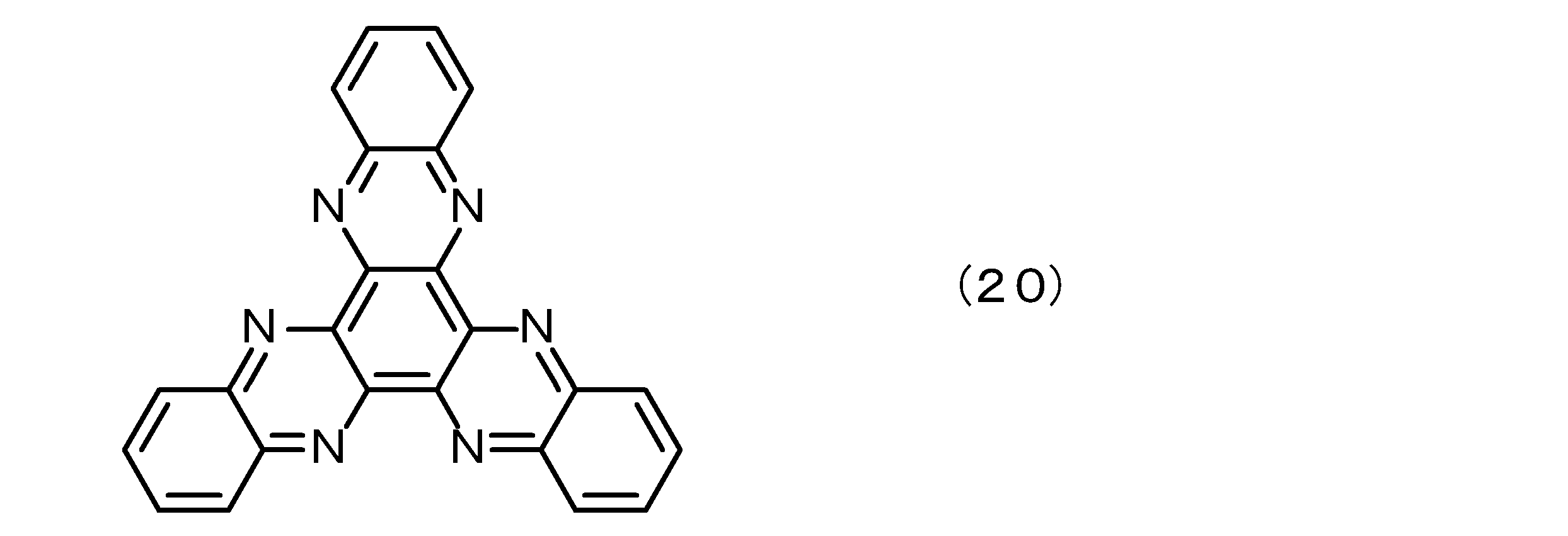
- the n-type organic semiconductor material “HATNA” having the following structural formula (20), which is a transparent material, was used.
- UV-visible absorption spectrum (UV-VIS) calculation by time-dependent density functional method (TD-DFT) was performed. More specifically, based on the six types of structures shown in FIG. 4, structure optimization calculation by Gaussian09 was performed. As a calculation level, a B3LYP functional was used, and 6-31 + G ** was used as a basis function. After structural optimization, UV-visible absorption spectrum (UV-VIS) calculations were performed using time-dependent density functional theory (TD-DFT) at the B3LYP / 6-31 + G ** level. The results are shown in Table 1 below.
- the spectroscopic characteristics are not significantly changed by introduction of substituents. From the calculation results, a slight shift was observed in some maximum peaks ( ⁇ max ), HOMO, and LUMO due to the introduction of substituents.
- the absorption of the maximum peak is a HOMO-LUMO transition, and HOMO and LUMO mainly have a large density on the DIP skeleton. In other words, it was found that the electronic structure of the basic molecule was not changed by the introduction of the substituent.
- spectroscopic measurement of the diindenoperylene derivative thin film having the structural formula (2) and the DIP thin film was performed using an ultraviolet-visible spectrophotometer.
- the sample for evaluation was obtained by forming a 50 nm-thick photoelectric conversion layer on a quartz substrate, and forming a 50-nm-thick ITO film on the photoelectric conversion layer.
- the spectroscopic measurement results are shown in FIG.
- the spectral shape of the DIP thin film (see “B” in FIG. 5) is broad overall.
- the diindenoperylene derivative thin film having the structural formula (2) has a maximum absorption peak in the range of 450 nm to 600 nm (see “A” in FIG. 5).
- the values of the external quantum efficiency (EQE) and the dark current in the image pickup devices of Examples 1A, 1B, 1C, 1A, and 1B were obtained. The results are shown in Table 2 below.
- the value of external quantum efficiency (EQE) was calculated from the measured value of dark current and the measured value of bright current. In the measurement of the dark current and the bright current, a high bias voltage such as ⁇ 5 volts was applied to the first electrode 21 and the second electrode 22 as a reverse bias voltage. The irradiation intensity at the time of measuring the bright current was set to 1.62 ⁇ W / cm 2, and the irradiation intensity at the time of measuring the dark current was set to 0.
- the photoelectric conversion layer 30 By constituting the photoelectric conversion layer 30 from a combination of an n-type organic semiconductor material having a LUMO value of 0.2 eV or more lower than the LUMO value of the diindenoperylene derivative having the structural formula (1), and a DIP derivative, It was confirmed that excellent photoelectric conversion characteristics and low dark current characteristics can be imparted to the image sensor.
- Table 3 below shows HOMO values (unit: eV) measured by ultraviolet light atomic spectroscopy (UPS) and LUMO values (unit: eV) calculated from the optical band gap.
- spectral characteristics were evaluated using an IPCE measuring apparatus. Specifically, the wavelength (unit: nm) of the irradiation intensity as 5.0 ⁇ W / cm 2 obtains the spectral sensitivity (1) as a parameter, the wavelength of the radiation intensity as a 1.62 ⁇ W / cm 2 (unit: nm) parameters As a result, spectral sensitivity (2) was obtained. A reverse bias voltage of ⁇ 1 volt was applied between the first electrode 21 and the second electrode 22. The obtained results are shown in FIG. 6A, FIG. 6B and FIG. Incidentally, FIG.
- FIG. 2 is a conceptual diagram of the solid-state imaging device according to the first embodiment.
- the solid-state imaging device 40 according to the first embodiment includes an imaging region 41 in which the above-described imaging elements 11 are arranged in a two-dimensional array on a semiconductor substrate (for example, a silicon semiconductor substrate), and a vertical drive circuit 42 as a peripheral circuit thereof. , A column signal processing circuit 43, a horizontal drive circuit 44, an output circuit 45, a control circuit 46, and the like. Note that these circuits can be configured from well-known circuits, and can be configured using other circuit configurations (for example, various circuits used in conventional CCD imaging devices and CMOS imaging devices). Needless to say, it can be done.
- the control circuit 46 generates a clock signal and a control signal that serve as a reference for the operation of the vertical drive circuit 42, the column signal processing circuit 43, and the horizontal drive circuit 44 based on the vertical synchronization signal, the horizontal synchronization signal, and the master clock.
- the generated clock signal and control signal are input to the vertical drive circuit 42, the column signal processing circuit 43, and the horizontal drive circuit 44.
- the vertical drive circuit 42 is constituted by, for example, a shift register, and selectively scans each imaging element 11 in the imaging region 41 sequentially in the vertical direction in units of rows.
- a pixel signal based on a current (signal) generated according to the amount of light received by each image sensor 11 is sent to the column signal processing circuit 43 via the vertical signal line 47.
- the column signal processing circuit 43 is disposed, for example, for each column of the image sensor 11, and outputs a signal output from the image sensor 11 for one row for each image sensor as a black reference pixel (not shown, but in an effective pixel region). Signal processing for noise removal and signal amplification is performed by a signal from a surrounding signal.
- a horizontal selection switch (not shown) is connected between the horizontal signal line 48 and provided.
- the horizontal drive circuit 44 is configured by, for example, a shift register, and sequentially outputs each of the column signal processing circuits 43 by sequentially outputting horizontal scanning pulses, and a signal is output from each of the column signal processing circuits 43 to the horizontal signal line 48. Output.
- the output circuit 45 performs signal processing and outputs the signals sequentially supplied from each of the column signal processing circuits 43 via the horizontal signal line 48.
- the photoelectric conversion layer itself also functions as a color filter, color separation is possible without providing a color filter.
- the photoelectric conversion layer 30 is composed of a diindenoperylene (DIP) derivative.
- DIP diindenoperylene
- the light absorption is carried by the DIP skeleton, and the substituent acts as a steric hindrance.
- the optical properties at the monomolecular level are not substantially changed by the introduction of the substituent, the molecular aggregation state and the molecular orientation state are changed during the thin film formation, and as a result, the intermolecular interaction is changed. As a result, the spectral characteristics are changed. As a result, a maximum absorption peak appears at a desired position (450 nm to 6500 nm).
- the photoelectric conversion layer exhibits a high absorption peak for light having a wavelength of 450 nm to 600 nm. Furthermore, since the photoelectric conversion layer includes an organic semiconductor material that absorbs green, a maximum absorption peak can be imparted to a desired absorption band in the imaging element. As a result, a solid-state imaging device having excellent characteristics can be provided.
- Example 2 is a modification of the image sensor of Example 1, and relates to a multilayer image sensor of the present disclosure and a solid-state image sensor according to the second aspect of the present disclosure. That is, the stacked image sensor (vertical spectroscopic image sensor) of the second embodiment is formed by stacking one of the image sensors described in the first embodiment.
- the solid-state imaging device according to the second embodiment includes a plurality of such stacked imaging devices.
- the stacked image sensor of Example 2 includes the green image sensor described in Example 1 and the blue image sensor having the conventional configuration and structure. Three image sensors (three sub-pixels) of the red image sensor are stacked in the vertical direction.
- the stacking order is not limited to this.
- the green image sensor described in the first embodiment and the blue image sensor having the conventional configuration and structure are provided on a silicon semiconductor substrate, and the image sensor A structure in which one or a plurality of photoelectric conversion regions (an image pickup device, in the illustrated example, a photoelectric conversion region having sensitivity to red) is stacked inside a silicon semiconductor substrate located below, thereby stacking the image pickup devices. That is, it is possible to obtain a stacked image sensor having a structure in which subpixels are stacked to form one pixel.
- the green image pickup device described in the first embodiment is provided on a silicon semiconductor substrate, and a plurality of photoelectric conversion regions (image pickup devices) are provided inside the silicon semiconductor substrate located below the image pickup device.
- a stacked image pickup device having a structure in which image pickup devices are stacked, that is, a structure in which subpixels are stacked to form one pixel can be obtained.
- the green image pickup device described in the first embodiment is provided on a semiconductor substrate, and one photoelectric conversion region (image pickup device) is provided inside the semiconductor substrate located below the image pickup device. It is possible to obtain a multilayer imaging device having a structure in which the layers are stacked.
- a blue imaging device having a conventional configuration and structure, a conventional configuration, a red imaging device having a structure, a conventional configuration, An imaging element having sensitivity to infrared rays having a structure can be given.
- the semiconductor substrate include a silicon semiconductor substrate and a compound semiconductor substrate.
- the photoelectric conversion region (imaging device) formed on the silicon semiconductor substrate is preferably a back-side illuminated type, but can also be a front-side illuminated type.
- the photoelectric conversion region can be formed on the semiconductor substrate by an epitaxial growth method, or can be formed on a silicon layer in a so-called SOI structure.
- the first electrode is made of a transparent conductive material such as ITO in the upper image sensor so as not to prevent light reception by the lower image sensor.
- the two electrodes are also made of a transparent conductive material such as ITO.
- the solid-state imaging device including the multilayer imaging device, a plurality of types of light are incident in the same pixel instead of performing blue, green, and red spectroscopy using a color filter. Since the imaging elements having sensitivity to light having a wavelength are stacked, it is possible to improve sensitivity and pixel density per unit volume. In addition, since the organic semiconductor material has a high absorption coefficient, the film thickness of the photoelectric conversion layer can be made thinner than that of a conventional Si-based photoelectric conversion layer, and light leakage from adjacent pixels and the limitation on the incident angle of light. Is alleviated. Further, in the conventional Si-based image pickup device, false color is generated because interpolation processing is performed between pixels of three colors to generate a color signal. Therefore, the generation of false colors can be suppressed.
- the present disclosure has been described based on the preferred embodiments, the present disclosure is not limited to these embodiments.
- the structures and configurations, manufacturing conditions, manufacturing methods, and materials used of the imaging device, the multilayer imaging device, and the solid-state imaging device described in the embodiments are examples, and can be changed as appropriate.
- first embodiment >> Comprising a first electrode, a second electrode, and a photoelectric conversion layer disposed between the first electrode and the second electrode;
- the photoelectric conversion layer A diindenoperylene derivative having a maximum absorption peak in a wavelength range of 450 nm to 600 nm and having the following structural formula (1); and Organic semiconductor material that absorbs green color, Consisting of An imaging device that takes out current generated in the photoelectric conversion layer by light irradiation to the outside through the first electrode and the second electrode by applying a voltage to the first electrode and the second electrode.
- X 1 to X 8 are each independently an alkyl group that may have a substituent, a heteroalkyl group, an aryl group that may have a substituent, a heteroaryl group, a carbocyclic compound, or a heterocyclic compound.
- X 1 to X 8 are each independently an alkyl group that may have a substituent, a heteroalkyl group, an aryl group that may have a substituent, a heteroaryl group, a carbocyclic compound, or a heterocyclic compound.
- n-type organic semiconductor material includes the following structural formula (10).
- X and R 1 to R 12 are each independently a hydrogen atom; a halogen atom containing chlorine and fluorine; or a linear, branched or cyclic alkyl group or phenyl group; a linear or condensed aromatic A ring, a partial fluoroalkyl group, a perfluoroalkyl group, a silylalkyl group, a silylalkoxy group, an arylsilyl group, a thioalkyl group, a thioaryl group, an arylsulfonyl group, an alkylsulfonyl group, an amino group, an alkylamino group, an arylamino group, a hydroxy An alkoxy group; an acylamino group; an acyloxy group; a carboxy group; a carboxamide
- [A09] The imaging device according to any one of [A01] to [A08], wherein the first electrode and the second electrode are made of a transparent conductive material.
- [A10] The imaging device according to any one of [A01] to [A08], in which one of the first electrode and the second electrode is made of a transparent conductive material and the other is made of a metal material.
- Solid-state imaging device first aspect >> [A01] to [A10] A solid-state imaging device including a plurality of imaging devices according to any one of [A01] to [A10].
- Solid-state imaging device second aspect >> A solid-state imaging device including a plurality of the multilayer imaging elements according to [B01].
Landscapes
- Solid State Image Pick-Up Elements (AREA)
- Light Receiving Elements (AREA)
Abstract
撮像素子は、第1電極21、第2電極22、及び、第1電極21と第2電極22との間に配設された光電変換層30を備えており、光電変換層30は、450nm乃至600nmの波長範囲に最大吸収ピークを有し、下記の構造式(1)を有するジインデノペリレン誘導体、及び、緑色を吸収するn型有機材料から成り、第1電極21及び第2電極22に電圧を印加することで、光照射によって光電変換層30において生じた電流を第1電極21及び第2電極22を介して外部に取り出す。
Description
本開示は、撮像素子、積層型撮像素子及び固体撮像装置に関する。
光電変換層に有機半導体材料を用いる撮像素子は、特定の色(波長帯)を光電変換することが可能である。そして、このような特徴を有するが故に、固体撮像装置における撮像素子として用いる場合、オンチップカラーフィルター(OCCF)と撮像素子との組合せから副画素が成り、副画素が2次元配列されている、従来の固体撮像装置では不可能な、副画素を積層した構造(積層型撮像素子)を得ることが可能である。また、デモザイク処理を必要としないことから、偽色が発生しないといった利点がある。
ところで、撮像素子には、外部量子効率(EQE)が高いこと、暗電流が低いこと(高いS/N比を有すること)が求められる。外部量子効率を増加させるためには、通常、光電変換層に印加するバイアス電圧を高くする。然るに、バイアス電圧を高くすると、暗電流が増加するといった問題がある。
太陽電池の光活性領域をジインデノペリレン(DIP)から構成する技術が、例えば、特表2014-506736から周知である。
DIPは、高いホール移動度を有する材料である。しかしながら、撮像素子の光電変換層をDIPから構成した場合、優れた分光特性を得ることができない。即ち、例えば、450nm乃至600nmの波長を有する光に対する高い吸収ピークを光電変換層は示さないし、光の吸収量が少ないといった問題がある(図5参照)。
従って、本開示の目的は、高い外部量子効率、低い暗電流といった特性を有し、しかも、450nm乃至600nmの波長を有する光に対する高い吸収ピークを示す光電変換層を備えた撮像素子、係る撮像素子を有する積層型撮像素子、係る撮像素子あるいは積層型撮像素子を備えた固体撮像装置を提供することにある。
上記の目的を達成するための本開示の第1の態様に係る撮像素子は、
第1電極、第2電極、及び、第1電極と第2電極との間に配設された光電変換層を備えており、
光電変換層は、
450nm乃至600nmの波長範囲に最大吸収ピークを有し、下記の構造式(1)を有するジインデノペリレン誘導体、及び、
緑色を吸収する有機半導体材料、
から成り、
第1電極及び第2電極に電圧を印加することで、光照射によって光電変換層において生じた電流を第1電極及び第2電極を介して外部に取り出す。
第1電極、第2電極、及び、第1電極と第2電極との間に配設された光電変換層を備えており、
光電変換層は、
450nm乃至600nmの波長範囲に最大吸収ピークを有し、下記の構造式(1)を有するジインデノペリレン誘導体、及び、
緑色を吸収する有機半導体材料、
から成り、
第1電極及び第2電極に電圧を印加することで、光照射によって光電変換層において生じた電流を第1電極及び第2電極を介して外部に取り出す。
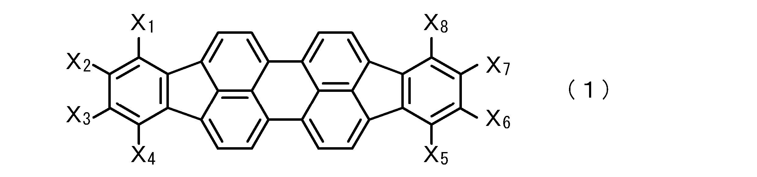
X1乃至X8は、それぞれ、独立に、置換基を有することあるアルキル基、ヘテロアルキル基、置換基を有することあるアリール基、ヘテロアリール基、炭素環式化合物、又は、複素環式化合物から成る。
上記の目的を達成するための本開示の第2の態様に係る撮像素子は、
第1電極、第2電極、及び、第1電極と第2電極との間に配設された光電変換層を備えており、
光電変換層は、「P4-Ph4-DIP」と略称される下記の構造式(2)を有するジインデノペリレン誘導体、及び、「F6SubPc-Cl」と略称される下記の構造式(14)を有するn型有機半導体材料から成るバルクヘテロ層から構成されている。
第1電極、第2電極、及び、第1電極と第2電極との間に配設された光電変換層を備えており、
光電変換層は、「P4-Ph4-DIP」と略称される下記の構造式(2)を有するジインデノペリレン誘導体、及び、「F6SubPc-Cl」と略称される下記の構造式(14)を有するn型有機半導体材料から成るバルクヘテロ層から構成されている。


上記の目的を達成するための本開示の積層型撮像素子は、本開示の第1の態様~第2の態様に係る撮像素子が、1つ、積層されて成る。
上記の目的を達成するための本開示の第1の態様に係る固体撮像装置は、本開示の第1の態様~第2の態様に係る撮像素子を、複数、備えている。また、上記の目的を達成するための本開示の第2の態様に係る固体撮像装置は、本開示の積層型撮像素子を、複数、備えている。
本開示の第1の態様~第2の態様に係る撮像素子、本開示の積層型撮像素子を構成する撮像素子、本開示の第1の態様~第2の態様に係る固体撮像装置を構成する撮像素子(以下、これらを総称して、『本開示の撮像素子等』と呼ぶ場合がある)にあっては、光電変換層をジインデノペリレン(DIP)誘導体から構成するので、光電変換層に高いホール移動度、高い外部量子効率、低い暗電流といった特性を付与することができる。しかも、光電変換層は、450nm乃至600nmの波長を有する光に対する高い吸収ピークを示す。それ故、優れた特性を有する固体撮像装置を提供することができる。尚、本明細書に記載された効果はあくまで例示であって限定されるものでは無く、また、付加的な効果があってもよい。
以下、図面を参照して、実施例に基づき本開示を説明するが、本開示は実施例に限定されるものではなく、実施例における種々の数値や材料は例示である。尚、説明は、以下の順序で行う。
1.本開示の第1の態様~第2の態様に係る撮像素子、本開示の積層型撮像素子、本開示の第1の態様~第2の態様に係る固体撮像装置、全般に関する説明
2.実施例1(本開示の第1の態様~第2の態様に係る撮像素子、及び、本開示の第1の態様に係る固体撮像装置)
3.実施例2(本開示の積層型撮像素子、及び、本開示の第2の態様に係る固体撮像装置)
4.その他
1.本開示の第1の態様~第2の態様に係る撮像素子、本開示の積層型撮像素子、本開示の第1の態様~第2の態様に係る固体撮像装置、全般に関する説明
2.実施例1(本開示の第1の態様~第2の態様に係る撮像素子、及び、本開示の第1の態様に係る固体撮像装置)
3.実施例2(本開示の積層型撮像素子、及び、本開示の第2の態様に係る固体撮像装置)
4.その他
〈本開示の第1の態様~第2の態様に係る撮像素子、本開示の積層型撮像素子、本開示の第1の態様~第2の態様に係る固体撮像装置、全般に関する説明〉
本開示の第1の態様に係る撮像素子、本開示の積層型撮像素子を構成する本開示の第1の態様に係る撮像素子、本開示の第1の態様に係る固体撮像装置を構成する本開示の第1の態様に係る撮像素子(以下、これらを総称して、『本開示の第1の態様に係る撮像素子等』と呼ぶ場合がある)において、n型有機半導体材料のLUMO値は、構造式(1)を有するジインデノペリレン誘導体のLUMO値よりも、0.2eV以上低いことが好ましい。
本開示の第1の態様に係る撮像素子、本開示の積層型撮像素子を構成する本開示の第1の態様に係る撮像素子、本開示の第1の態様に係る固体撮像装置を構成する本開示の第1の態様に係る撮像素子(以下、これらを総称して、『本開示の第1の態様に係る撮像素子等』と呼ぶ場合がある)において、n型有機半導体材料のLUMO値は、構造式(1)を有するジインデノペリレン誘導体のLUMO値よりも、0.2eV以上低いことが好ましい。
上記の好ましい形態を含む本開示の撮像素子等において、光電変換層はバルクヘテロ構造を有する構成とすることができる。
以上に説明した好ましい形態、構成を含む本開示の第1の態様に係る撮像素子等において、n型有機半導体材料は下記の構造式(10)から成る形態とすることができる。そして、この場合、n型有機半導体材料は、具体的には、下記の構造式(11)、より具体的には、「SubPc-Cl」と略称される下記の構造式(12)から成る形態とすることができるし、あるいは又、「F12SubPc-Cl」と略称される下記の構造式(13)から成る形態とすることができるし、あるいは又、「F6SubPc-Cl」と略称される下記の構造式(14)から成る形態とすることができる。


以上に説明した好ましい形態、構成を含む本開示の撮像素子等において、構造式(1)あるいは構造式(2)を有するジインデノペリレン誘導体(以下、これらを総称して、『DIP誘導体等』と呼ぶ)は、p型半導体材料としての性質を有する。尚、有機半導体は、p型、n型と分類されることが多いが、p型とは正孔を輸送し易いという意味であり、n型とは電子を輸送し易いという意味であり、無機半導体のように熱励起の多数キャリアとして正孔又は電子を有しているという解釈に限定されない。光電変換層には、更に、p型半導体材料及び/又はn型半導体材料が含まれていてもよい。
更には、以上に説明した好ましい形態、構成を含む本開示の撮像素子等において、第1電極及び第2電極は透明導電材料から成る構成とすることができる。あるいは又、第1電極及び第2電極のいずれか一方は透明導電材料から成り、他方は金属材料から成る構成とすることができる。
本開示の撮像素子等において、光入射側の電極は透明導電材料から成る構成とすることが好ましい。係る電極を『透明電極』と呼ぶ。ここで、透明電極を構成する透明導電材料として、インジウム-錫酸化物(ITO,SnドープのIn2O3、結晶性ITO及びアモルファスITOを含む)、IFO(FドープのIn2O3)、酸化錫(SnO2)、ATO(SbドープのSnO2)、FTO(FドープのSnO2)、酸化亜鉛(AlドープのZnOやBドープのZnO、GaドープのZnOを含む)、酸化インジウム-酸化亜鉛(IZO)、酸化チタン(TiO2)、スピネル形酸化物、YbFe2O4構造を有する酸化物を例示することができる。
透明性が不要である場合、第1電極あるいは第2電極を構成する導電材料として、第1電極あるいは第2電極をカソード電極(陰極)として機能させる場合、即ち、正孔を取り出す電極として機能させる場合、高仕事関数(例えば、φ=4.5eV~5.5eV)を有する導電材料から構成することが好ましく、具体的には、金(Au)、銀(Ag)、クロム(Cr)、ニッケル(Ni)、パラジウム(Pd)、白金(Pt)、鉄(Fe)、イリジウム(Ir)、ゲルマニウム(Ge)、オスミウム(Os)、レニウム(Re)、テルル(Te)を例示することができる。一方、第1電極あるいは第2電極をアノード(陽極)として機能させる場合、即ち、電子を取り出す電極として機能させる場合、低仕事関数(例えば、φ=3.5eV~4.5eV)を有する導電材料から構成することが好ましく、具体的には、アルカリ金属(例えばLi、Na、K等)及びそのフッ化物又は酸化物、アルカリ土類金属(例えばMg、Ca等)及びそのフッ化物又は酸化物、アルミニウム(Al)、亜鉛(Zn)、錫(Sn)、タリウム(Tl)、ナトリウム-カリウム合金、アルミニウム-リチウム合金、マグネシウム-銀合金、インジウム、イッテリビウム等の希土類金属、あるいは、これらの合金を挙げることができる。あるいは又、第1電極や第2電極を構成する材料として、白金(Pt)、金(Au)、パラジウム(Pd)、クロム(Cr)、ニッケル(Ni)、アルミニウム(Al)、銀(Ag)、タンタル(Ta)、タングステン(W)、銅(Cu)、チタン(Ti)、インジウム(In)、錫(Sn)、鉄(Fe)、コバルト(Co)、モリブデン(Mo)等の金属、あるいは、これらの金属元素を含む合金、これらの金属から成る導電性粒子、これらの金属を含む合金の導電性粒子、不純物を含有したポリシリコン、炭素系材料、酸化物半導体、カーボン・ナノ・チューブ、グラフェン等の導電性物質を挙げることができるし、これらの元素を含む層の積層構造とすることもできる。更には、第1電極や第2電極を構成する材料として、ポリ(3,4-エチレンジオキシチオフェン)/ポリスチレンスルホン酸[PEDOT/PSS]といった材料(導電性高分子)を挙げることもできる。また、これらの導電性材料をバインダー(高分子)に混合してペースト又はインクとしたものを硬化させ、電極として用いてもよい。
第1電極や第2電極の形成方法として、これらを構成する材料にも依るが、各種のPVD法;MOCVD法を含む各種のCVD法;各種の塗布法;ディップ法;パイロゾル法;有機金属化合物を熱分解する方法;リフト・オフ法;ゾル-ゲル法;電着法;シャドウマスク法;電解メッキ法や無電解メッキ法あるいはこれらの組合せといったメッキ法;及び、スプレー法の内のいずれかと、必要に応じてパターニング技術との組合せを挙げることができる。第1電極や第2電極の表面を、酸素プラズマ、アルゴンプラズマ、窒素プラズマ、オゾン等で処理することもできる。これらの処理は、被覆層(後述する)の有無、被覆前後に関係無く、実施することができる。PVD法として、電子ビーム加熱法、電子ビーム蒸着法、抵抗加熱法、フラッシュ蒸着法、反応性蒸着法等の各種真空蒸着法;プラズマ蒸着法;2極スパッタリング法、直流スパッタリング法、直流マグネトロンスパッタリング法、高周波スパッタリング法、マグネトロンスパッタリング法、イオンビームスパッタリング法、バイアススパッタリング法等の各種スパッタリング法;DC(direct current)法、RF法、多陰極法、活性化反応法、電界蒸着法、高周波イオンプレーティング法、反応性イオンプレーティング法等の各種イオンプレーティング法を挙げることができる。塗布法として、具体的には、スピンコート法;浸漬法;キャスト法;スクリーン印刷法やインクジェット印刷法、オフセット印刷法、グラビア印刷法といった各種印刷法;スタンプ法;スプレー法;エアドクタコーター法、ブレードコーター法、ロッドコーター法、ナイフコーター法、スクイズコーター法、リバースロールコーター法、トランスファーロールコーター法、グラビアコーター法、キスコーター法、キャストコーター法、スプレーコーター法、スリットオリフィスコーター法、カレンダーコーター法といった各種コーティング法を例示することができる。
本開示の撮像素子等にあっては、第1電極と第2電極との間に、第1バッファ層/光電変換層/第2バッファ層が形成されている形態、光電変換層/第2バッファ層が形成されている形態とすることができる。あるいは又、本開示の撮像素子等にあっては、第1電極と第2電極との間に、第1バッファ層/n型有機材料層/光電変換層/p型有機材料層/第2バッファ層が形成されている形態とすることができる。あるいは又、本開示の撮像素子等にあっては、第1電極と第2電極との間に、正孔ブロッキング層/光電変換層/電子ブロッキング層が形成されている形態とすることができる。第2バッファ層を無機材料から構成する場合、係る無機材料として例えば、リチウム(Li)、ナトリウム(Na)、カリウム(K)といったアルカリ金属及びそのフッ化物や酸化物、マグネシウム(Mg)、カルシウム(Ca)といったアルカリ土類金属及びそのフッ化物や酸化物を挙げることができる。
以上に説明した好ましい形態、構成を含む本開示の撮像素子等にあっては、
透明導電材料から成る第1電極は、透明な基板上に形成されており、
光電変換層は、第1電極上に形成されており、
第2電極は、光電変換層上に形成されている構成とすることができる。あるいは又、
第1電極は、基板上に形成されており、
光電変換層は、第1電極上に形成されており、
透明導電材料から成る第2電極は、光電変換層上に形成されている構成とすることができる。ここで、第1電極と第2電極とは離間されているが、係る離間状態として、第1電極の上方に第2電極が設けられている形態を挙げることができる。
透明導電材料から成る第1電極は、透明な基板上に形成されており、
光電変換層は、第1電極上に形成されており、
第2電極は、光電変換層上に形成されている構成とすることができる。あるいは又、
第1電極は、基板上に形成されており、
光電変換層は、第1電極上に形成されており、
透明導電材料から成る第2電極は、光電変換層上に形成されている構成とすることができる。ここで、第1電極と第2電極とは離間されているが、係る離間状態として、第1電極の上方に第2電極が設けられている形態を挙げることができる。
光電変換層は、共蒸着法に基づき形成(成膜)することが好ましいが、このような方法に限定するものではない。
光電変換層の厚さは、限定するものではないが、例えば、1×10⁻⁸m乃至5×10⁻⁷m、好ましくは2.5×10⁻⁸m乃至3×10⁻⁷m、より好ましくは2.5×10⁻⁸m乃至2×10⁻⁷m、一層好ましくは1×10⁻⁷m乃至1.8×10⁻⁷mを例示することができる。
基板として、ポリメチルメタクリレート(ポリメタクリル酸メチル,PMMA)やポリビニルアルコール(PVA)、ポリビニルフェノール(PVP)、ポリエーテルスルホン(PES)、ポリイミド、ポリカーボネート(PC)、ポリエチレンテレフタレート(PET)、ポリエチレンナフタレート(PEN)に例示される有機ポリマー(高分子材料から構成された可撓性を有するプラスチック・フィルムやプラスチック・シート、プラスチック基板といった高分子材料の形態を有する)を挙げることができ、あるいは又、雲母を挙げることができる。このような可撓性を有する高分子材料から構成された基板を使用すれば、例えば曲面形状を有する電子機器への電子デバイスの組込みあるいは一体化が可能となる。あるいは又、基板として、各種ガラス基板や、表面に絶縁膜が形成された各種ガラス基板、石英基板、表面に絶縁膜が形成された石英基板、表面に絶縁膜が形成されたシリコン基板、ステンレス等の各種合金や各種金属から成る金属基板を挙げることができる。尚、絶縁膜として、酸化ケイ素系材料(例えば、SiOXやスピンオンガラス(SOG));窒化ケイ素(SiNY);酸窒化ケイ素(SiON);酸化アルミニウム(Al2O3);金属酸化物や金属塩を挙げることができる。また、表面にこれらの絶縁膜が形成された導電性基板(金やアルミニウム等の金属から成る基板、高配向性グラファイトから成る基板)を用いることもできる。基板の表面は、平滑であることが望ましいが、光電変換層の特性に悪影響を及ぼさない程度のラフネスがあっても構わない。基板の表面にシランカップリング法によるシラノール誘導体を形成したり、SAM法等によりチオール誘導体、カルボン酸誘導体、リン酸誘導体等から成る薄膜を形成したり、CVD法等により絶縁性の金属塩や金属錯体から成る薄膜を形成することで、第1電極や第2電極と基板との間の密着性を向上させてもよい。透明な基板とは、基板を介して光電変換層に入射する光を過度に吸収しない材料から構成された基板を指す。
場合によっては、電極や光電変換層を被覆層で被覆してもよい。被覆層を構成する材料として、酸化ケイ素系材料;窒化ケイ素(SiNY);酸化アルミニウム(Al2O3)等の金属酸化物高誘電絶縁膜にて例示される無機系絶縁材料だけでなく、ポリメチルメタクリレート(PMMA);ポリビニルフェノール(PVP);ポリビニルアルコール(PVA);ポリイミド;ポリカーボネート(PC);ポリエチレンテレフタレート(PET);ポリスチレン;N-2(アミノエチル)3-アミノプロピルトリメトキシシラン(AEAPTMS)、3-メルカプトプロピルトリメトキシシラン(MPTMS)、オクタデシルトリクロロシラン(OTS)等のシラノール誘導体(シランカップリング剤);オクタデカンチオール、ドデシルイソシアネイト等の一端に電極と結合可能な官能基を有する直鎖炭化水素類にて例示される有機系絶縁材料(有機ポリマー)を挙げることができるし、これらの組み合わせを用いることもできる。尚、酸化ケイ素系材料として、酸化シリコン(SiOX)、BPSG、PSG、BSG、AsSG、PbSG、酸化窒化シリコン(SiON)、SOG(スピンオングラス)、低誘電率材料(例えば、ポリアリールエーテル、シクロパーフルオロカーボンポリマー及びベンゾシクロブテン、環状フッ素樹脂、ポリテトラフルオロエチレン、フッ化アリールエーテル、フッ化ポリイミド、アモルファスカーボン、有機SOG)を例示することができる。
固体撮像装置は、表面照射型とすることもできるし、裏面照射型とすることもでき、また、単板式カラー固体撮像装置を構成することができる。固体撮像装置を構成する撮像素子として撮像素子を集積化する場合、PLD法(パルスレーザーデポジション法)に基づきパターンを形成する方法を採用することもできる。撮像素子には、その他、必要に応じて、オンチップ・マイクロ・レンズや遮光層を設けてもよいし、撮像素子を駆動するための駆動回路や配線が設けられている。必要に応じて、撮像素子への光の入射を制御するためのシャッターを配設してもよいし、固体撮像装置の目的に応じて光学カットフィルターを具備してもよい。更には、本開示の固体撮像装置における撮像素子を本開示の撮像素子の単層から構成する場合、撮像素子の配列として、ベイヤ配列、インターライン配列、GストライプRB市松配列、GストライプRB完全市松配列、市松補色配列、ストライプ配列、斜めストライプ配列、原色色差配列、フィールド色差順次配列、フレーム色差順次配列、MOS型配列、改良MOS型配列、フレームインターリーブ配列、フィールドインターリーブ配列を挙げることができる。尚、本開示の撮像素子等によって、テレビカメラ等の固体撮像装置以外にも、光センサーやイメージセンサーを構成することができる。
実施例1は、本開示の第1の態様~第2の態様に係る撮像素子、及び、本開示の第1の態様に係る固体撮像装置に関する。
実施例1の撮像素子(緑色用撮像素子)11は、図1に模式的な断面図を示すように、第1電極21、第2電極22、及び、第1電極21と第2電極22との間に配設された光電変換層30を備えている。即ち、実施例1の撮像素子11は、
(a-1)離間して設けられた第1電極21及び第2電極22、及び、
(a-2)第1電極21と第2電極22との間に設けられた光電変換層30、
を備えている。そして、光電変換層30は、450nm乃至600nmの波長範囲に最大吸収ピークを有し、前述した構造式(1)を有するジインデノペリレン誘導体、及び、緑色を吸収する有機半導体材料(具体的には、n型有機半導体材料)から成り、第1電極21及び第2電極22に電圧を印加することで、光照射によって光電変換層30において生じた電流を第1電極21及び第2電極22を介して外部に取り出す。
(a-1)離間して設けられた第1電極21及び第2電極22、及び、
(a-2)第1電極21と第2電極22との間に設けられた光電変換層30、
を備えている。そして、光電変換層30は、450nm乃至600nmの波長範囲に最大吸収ピークを有し、前述した構造式(1)を有するジインデノペリレン誘導体、及び、緑色を吸収する有機半導体材料(具体的には、n型有機半導体材料)から成り、第1電極21及び第2電極22に電圧を印加することで、光照射によって光電変換層30において生じた電流を第1電極21及び第2電極22を介して外部に取り出す。
あるいは又、実施例1の撮像素子(緑色用撮像素子)11は、第1電極21、第2電極22、及び、第1電極21と第2電極22との間に配設された光電変換層30を備えており、光電変換層30は、「P4-Ph4-DIP」と略称される前述した構造式(2)を有するジインデノペリレン誘導体、及び、「F6SubPc-Cl」と略称される前述した構造式(14)を有するn型有機半導体材料から成るバルクヘテロ層から構成されている。尚、構造式(2)は、構造式(1)におけるX1,X4,X5,X8をフェニル基とし、X2,X3,X7,X8をプロピル基としたジインデノペリレン誘導体である。ここで、光電変換層30は、真空蒸着法、具体的には、共蒸着法にて成膜することができる。
構造式(2)を有するジインデノペリレン誘導体の合成スキームの概略を図3に示す。
光入射側の電極である第1電極21は、透明導電材料、具体的には、厚さ50nmのインジウム-錫酸化物(ITO)から成る。また、第2電極22は、厚さ100nmのAl-Si-Cuから成る。透明導電材料から成る第1電極21は、透明な基板20上に形成されており、光電変換層30は第1電極21上に形成されており、第2電極21は光電変換層30上に形成されている。このように、第1電極21の上方に第2電極22が設けられている。光は、基板20及び第1電極21を介して光電変換層30に入射する。基板20は厚さ0.7mmの石英基板から成る。
実施例1の撮像素子11は、以下の方法で作製することができる。即ち、先ず、石英基板から成る基板20上に、スパッタリング装置を用いてITO膜を成膜し、フォトリソグラフィ技術及びエッチング技術に基づき、ITO膜から成る第1電極(陽極)21を得た。次いで、基板20及び第1電極21上に絶縁層31を形成し、フォトリソグラフィ技術及びエッチング技術に基づき絶縁層31をパターニングすることで、1mm角の第1電極21を露出させた後、洗剤、アセトン、エタノールを用いて超音波洗浄を行った。そして、基板を乾燥後、更に、紫外線/オゾン処理を10分間行った。次いで、基板20を真空蒸着装置の基板ホルダーに固定し、蒸着槽を5.5×10-5Paに減圧した。
〈実施例1A〉、〈実施例1B〉、〈実施例1C〉
その後、シャドーマスクを用いた真空蒸着法に基づき、構造式(1)あるいは構造式(2)を有するp型のジインデノペリレン誘導体(DIP誘導体等)、及び、緑色を吸収する有機半導体材料から成る光電変換層30を、第1電極21上に成膜した。具体的には、蒸着速度比1:1で共蒸着法にて成膜することで、厚さ100nmの混合層(バルクヘテロ構造)から成る光電変換層30を得た。緑色を吸収する有機半導体材料(具体的には、n型有機半導体材料)は、具体的には、前述した構造式(10)から成り、具体的には、前述した構造式(11)、より具体的には、「SubPc-Cl」と略称される前述した構造式(12)から成り〈実施例1A〉、あるいは又、「F6SubPc-Cl」と略称される前述した構造式(14)から成り〈実施例1B〉、あるいは又、「F12SubPc-Cl」と略称される前述した構造式(13)から成る〈実施例1C〉。
その後、シャドーマスクを用いた真空蒸着法に基づき、構造式(1)あるいは構造式(2)を有するp型のジインデノペリレン誘導体(DIP誘導体等)、及び、緑色を吸収する有機半導体材料から成る光電変換層30を、第1電極21上に成膜した。具体的には、蒸着速度比1:1で共蒸着法にて成膜することで、厚さ100nmの混合層(バルクヘテロ構造)から成る光電変換層30を得た。緑色を吸収する有機半導体材料(具体的には、n型有機半導体材料)は、具体的には、前述した構造式(10)から成り、具体的には、前述した構造式(11)、より具体的には、「SubPc-Cl」と略称される前述した構造式(12)から成り〈実施例1A〉、あるいは又、「F6SubPc-Cl」と略称される前述した構造式(14)から成り〈実施例1B〉、あるいは又、「F12SubPc-Cl」と略称される前述した構造式(13)から成る〈実施例1C〉。
その後、真空蒸着装置を用いて、厚さ100nmのAl-Si-Cuから成る第2電極(陰極)22を成膜することで、図1に模式的な一部断面図を示す実施例1の評価用の撮像素子を得た。
〈比較例1A〉
比較例1Aの撮像素子として、光電変換層30を、構造式(1)あるいは構造式(2)を有するジインデノペリレン誘導体の代わりにジインデノペリレン(DIP)から構成した。また、緑色を吸収する有機半導体材料として、「F6SubPc-Cl」と略称される前述した構造式(14)を用いた。
比較例1Aの撮像素子として、光電変換層30を、構造式(1)あるいは構造式(2)を有するジインデノペリレン誘導体の代わりにジインデノペリレン(DIP)から構成した。また、緑色を吸収する有機半導体材料として、「F6SubPc-Cl」と略称される前述した構造式(14)を用いた。
〈比較例1B〉
更には、比較例1Bの撮像素子として、光電変換層30を、構造式(2)を有するジインデノペリレン誘導体から構成した。また、n型有機半導体材料として、透明な材料である、下記の構造式(20)を有する「HATNA」を用いた。
更には、比較例1Bの撮像素子として、光電変換層30を、構造式(2)を有するジインデノペリレン誘導体から構成した。また、n型有機半導体材料として、透明な材料である、下記の構造式(20)を有する「HATNA」を用いた。
先ず、単分子レベルで、DIP置換基導入によるエネルギーレベル及び分光形状の変化を検証した。具体的には、時間依存密度汎関数法(TD-DFT)による紫外可視吸収スペクトル(UV-VIS)計算を行った。より具体的には、図4に示す6種類の構造に基づき、Gaussian09による構造最適化計算を実行した。計算レベルは、B3LYP汎関数を使用し、基底関数には6-31+G**を使用した。構造適化後、B3LYP/6-31+G**レベルで時間依存密度汎関数法(TD-DFT)を使用し、紫外可視吸収スペクトル(UV-VIS)計算を実行した。その結果を、以下の表1に示す。
単分子レベルでは、置換基導入により分光特性が大きく変化しないことが好ましい。 計算結果から、置換基導入により若干の極大ピーク(λmax)、HOMO、LUMOに若干シフトが確認された。極大ピークの吸収はHOMO-LUMO遷移であり、HOMO、LUMOは主にDIP骨格上に大きな密度を有する。つまり、置換基導入により基本的な分子の電子構造は変化しないことが判った。
〈表1〉
λmax (nm) HOMO(eV) LUMO(eV)
構造(a) 535.45 -5.40 -2.92
構造(b) 554.70 -5.11 -2.66
構造(c) 553.65 -5.11 -2.66
構造(d) 562.18 -5.23 -2.80
構造(e) 550.02 -5.23 -2.77
構造(f) 566.16 -5.05 -2.65
λmax (nm) HOMO(eV) LUMO(eV)
構造(a) 535.45 -5.40 -2.92
構造(b) 554.70 -5.11 -2.66
構造(c) 553.65 -5.11 -2.66
構造(d) 562.18 -5.23 -2.80
構造(e) 550.02 -5.23 -2.77
構造(f) 566.16 -5.05 -2.65
次に、構造式(2)を有するジインデノペリレン誘導体薄膜、及び、DIP薄膜の分光測定を、紫外可視分光光度計を用いて行った。尚、評価用試料は、石英基板上に、厚さ50nm光電変換層を成膜し、光電変換層上に厚さ50nmのITOを成膜することで得た。分光測定結果を図5に示す。DIP薄膜の分光形状(図5の「B」参照)は、全体的にブロードである。一方、構造式(2)を有するジインデノペリレン誘導体薄膜は450nm乃至600nmの範囲に極大吸収ピークを有していることが示された(図5の「A」参照)。上述したTD-DFTによるUV-VIS計算、及び、分光測定の結果から、ジインデノペリレンへの置換基導入による立体障害が薄膜形成時の分光特性に影響を及ぼしていることが明らかになった。
更には、上記の実施例1A、実施例1B、実施例1C、比較例1A,比較例1Bの撮像素子における外部量子効率(EQE)の値及び暗電流の値を求めた。その結果を、以下の表2に示す。尚、外部量子効率(EQE)の値は、暗電流の測定値及び明電流の測定値から算出した。暗電流及び明電流の測定においては、第1電極21及び第2電極22に逆バイアス電圧として-5ボルトといった高いバイアス電圧を印加した。また、明電流測定時の照射強度を1.62μW/cm2とし、暗電流測定時の照射強度を0とした。
〈表2〉
EQE(%) 暗電流(A/cm2)
実施例1A 16 1.7×10⁻⁹
実施例1B 53 1.5×10⁻⁹
実施例1C 18 1.8×10⁻⁹
比較例1A 74 2.5×10⁻⁷
比較例1B 0.4 1.3×10⁻⁷
EQE(%) 暗電流(A/cm2)
実施例1A 16 1.7×10⁻⁹
実施例1B 53 1.5×10⁻⁹
実施例1C 18 1.8×10⁻⁹
比較例1A 74 2.5×10⁻⁷
比較例1B 0.4 1.3×10⁻⁷
LUMO値が、構造式(1)を有するジインデノペリレン誘導体のLUMO値よりも0.2eV以上低いn型有機半導体材料と、DIP誘導体等との組み合わせから光電変換層30を構成することで、撮像素子に優れた光電変換特性、低い暗電流特性を付与することができることが確認された。尚、紫外線光原子分光(UPS)により測定したHOMO値(単位:eV)、及び、オプティカルバンドギャップから算出したLUMO値(単位:eV)を、以下の表3に示す。
〈表3〉
HOMO LUMO
DIP -5.4 -3.3
構造式(2) 〈P4-Ph4-DIP〉 -5.5 -3.5
構造式(12) 〈SubPc-Cl〉 -5.7 -3.7
構造式(13) 〈F6SubPc-Cl〉 -6.3 -4.2
構造式(14) 〈F12SubPc-Cl〉 -6.6 -4.5
構造式(20) 〈HATNA〉 -6.9 -3.8
HOMO LUMO
DIP -5.4 -3.3
構造式(2) 〈P4-Ph4-DIP〉 -5.5 -3.5
構造式(12) 〈SubPc-Cl〉 -5.7 -3.7
構造式(13) 〈F6SubPc-Cl〉 -6.3 -4.2
構造式(14) 〈F12SubPc-Cl〉 -6.6 -4.5
構造式(20) 〈HATNA〉 -6.9 -3.8
また、実施例1A及び実施例1Bの撮像素子において、IPCE測定装置を用いて分光特性を評価した。具体的には、照射強度を5.0μW/cm2として波長(単位:nm)をパラメータとして分光感度(1)を求め、照射強度を1.62μW/cm2として波長(単位:nm)をパラメータとして分光感度(2)を求めた。第1電極21と第2電極22との間に逆バイアス電圧-1ボルトを印加した。得られた結果を図6A、図6B及び図7に示す。尚、図6A、図6B及び図7において、「A」は照射強度を5.0μW/cm2としたときのデータであり、「B」は照射強度を1.62μW/cm2としたときのデータである。実施例1A、実施例1B、実施例1Cの撮像素子にあっては、極大吸収ピークが450nm乃至600nmの間にあり、緑色吸収を示すことが確認された。
図2に、実施例1の固体撮像装置の概念図を示す。実施例1の固体撮像装置40は、半導体基板(例えばシリコン半導体基板)上に、上述した撮像素子11が2次元アレイ状に配列された撮像領域41、並びに、その周辺回路としての垂直駆動回路42、カラム信号処理回路43、水平駆動回路44、出力回路45及び制御回路46等から構成されている。尚、これらの回路は周知の回路から構成することができるし、また、他の回路構成(例えば、従来のCCD撮像装置やCMOS撮像装置にて用いられる各種の回路)を用いて構成することができることは云うまでもない。
制御回路46は、垂直同期信号、水平同期信号及びマスタクロックに基づいて、垂直駆動回路42、カラム信号処理回路43及び水平駆動回路44の動作の基準となるクロック信号や制御信号を生成する。そして、生成されたクロック信号や制御信号は、垂直駆動回路42、カラム信号処理回路43及び水平駆動回路44に入力される。
垂直駆動回路42は、例えば、シフトレジスタによって構成され、撮像領域41の各撮像素子11を行単位で順次垂直方向に選択走査する。そして、各撮像素子11における受光量に応じて生成した電流(信号)に基づく画素信号は、垂直信号線47を介してカラム信号処理回路43に送られる。
カラム信号処理回路43は、例えば、撮像素子11の列毎に配置されており、1行分の撮像素子11から出力される信号を撮像素子毎に黒基準画素(図示しないが、有効画素領域の周囲に形成される)からの信号によって、ノイズ除去や信号増幅の信号処理を行う。カラム信号処理回路43の出力段には、水平選択スイッチ(図示せず)が水平信号線48との間に接続されて設けられる。
水平駆動回路44は、例えばシフトレジスタによって構成され、水平走査パルスを順次出力することによって、カラム信号処理回路43の各々を順次選択し、カラム信号処理回路43の各々から信号を水平信号線48に出力する。
出力回路45は、カラム信号処理回路43の各々から水平信号線48を介して順次供給される信号に対して、信号処理を行って出力する。
ここで、光電変換層それ自体がカラーフィルターとしても機能するので、カラーフィルターを配設しなくとも色分離が可能である。
以上に説明したように、光電変換層30をジインデノペリレン(DIP)誘導体から構成する。ここで、光吸収はDIP骨格が担い、置換基は立体障害として作用する。そして、置換基の導入により、単分子レベルの光学特性はほぼ変化しないものの、薄膜形成時、分子の凝集状態及び分子配向状態が変化し、分子間相互作用が変化する結果、分光特性が変わる。その結果、所望の位置(450nm乃至6500nm)に極大吸収ピークが現れる。そして、光電変換層に高いホール移動度、高い外部量子効率、低い暗電流といった特性を付与することができる。しかも、光電変換層は、450nm乃至600nmの波長を有する光に対する高い吸収ピークを示す。更には、光電変換層は緑色を吸収する有機半導体材料を含んでいるので、撮像素子に所望の吸収帯に極大吸収ピークを付与することができる。そして、以上の結果として、優れた特性を有する固体撮像装置を提供することができる。
実施例2は、実施例1の撮像素子の変形であるが、本開示の積層型撮像素子及び本開示の第2の態様に係る固体撮像装置に関する。即ち、実施例2の積層型撮像素子(縦分光方式の撮像素子)は、実施例1において説明した撮像素子が、1つ、積層されて成る。また、実施例2の固体撮像装置は、このような積層型撮像素子を、複数、備えている。具体的には、実施例2の積層型撮像素子は、概念図を図8Aに示すように、実施例1において説明した緑色用撮像素子、並びに、従来の構成、構造を有する青色用撮像素子及び赤色用撮像素子の3つの撮像素子(3つの副画素)が、垂直方向に積層された構成を有する。即ち、副画素を積層して1画素とする構造を有する積層型撮像素子を得ることができる。青色用撮像素子が最上層に位置し、緑色用撮像素子が中間に位置し、赤色用撮像素子が最下層に位置する。但し、積層順はこれに限定するものではない。
あるいは又、概念図を図8Bに示すように、実施例1において説明した緑色用撮像素子、及び、従来の構成、構造を有する青色用撮像素子をシリコン半導体基板の上に設け、係る撮像素子の下方に位置するシリコン半導体基板の内部に1又は複数の光電変換領域(撮像素子であり、図示した例では、赤色に感度を有する光電変換領域)を設けることで、撮像素子が積層化された構造、即ち、副画素を積層して1画素とする構造を有する積層型撮像素子を得ることができる。
あるいは又、実施例1において説明した緑色用撮像素子をシリコン半導体基板の上に設け、係る撮像素子の下方に位置するシリコン半導体基板の内部に複数の光電変換領域(撮像素子)を設けることで、撮像素子が積層化された構造、即ち、副画素を積層して1画素とする構造を有する積層型撮像素子を得ることができる。あるいは又、実施例1において説明した緑色用撮像素子を半導体基板の上に設け、係る撮像素子の下方に位置する半導体基板の内部に1つの光電変換領域(撮像素子)を設けることで、撮像素子が積層化された構造を有する積層型撮像素子を得ることができる。ここで、半導体基板の内部に設けられた1つの光電変換領域(撮像素子)として、従来の構成、構造を有する青色用撮像素子、従来の構成、構造を有する赤色用撮像素子、従来の構成、構造を有する赤外線に感度を有する撮像素子を挙げることができる。また、半導体基板として、シリコン半導体基板や化合物半導体基板を挙げることができる。
シリコン半導体基板に形成された光電変換領域(撮像素子)は、裏面照射型であることが好ましいが、表面照射型とすることもできる。シリコン半導体基板の内部に光電変換領域を設ける代わりに、光電変換領域を、エピタキシャル成長法にて半導体基板上に形成することもできるし、あるいは又、所謂SOI構造におけるシリコン層に形成することもできる。
実施例2の積層型撮像素子にあっては、下方に位置する撮像素子の受光を妨げないように、上方に位置する撮像素子において、第1電極は、例えばITOといった透明導電材料から成り、第2電極も、例えば、ITOといった透明導電材料から成る。
積層型撮像素子を備えた実施例2の固体撮像装置にあっては、カラーフィルターを用いて青色、緑色、赤色の分光を行うのではなく、同一画素内で光の入射方向において、複数種の波長の光に対して感度を有する撮像素子を積層するため、感度の向上及び単位体積当たりの画素密度の向上を図ることができる。また、有機半導体材料は吸収係数が高いため、光電変換層の膜厚を従来のSi系光電変換層と比較して薄くすることができ、隣接画素からの光漏れや、光の入射角の制限が緩和される。更には、従来のSi系撮像素子では3色の画素間で補間処理を行って色信号を作成するために偽色が生じるが、積層型撮像素子を備えた実施例2の固体撮像装置にあっては、偽色の発生が抑えられる。
以上、本開示を好ましい実施例に基づき説明したが、本開示はこれらの実施例に限定されるものではない。実施例にて説明した撮像素子、積層型撮像素子、固体撮像装置の構造や構成、製造条件、製造方法、使用した材料は例示であり、適宜変更することができる。
尚、本開示は、以下のような構成を取ることもできる。
[A01]《撮像素子:第1の態様》
第1電極、第2電極、及び、第1電極と第2電極との間に配設された光電変換層を備えており、
光電変換層は、
450nm乃至600nmの波長範囲に最大吸収ピークを有し、下記の構造式(1)を有するジインデノペリレン誘導体、及び、
緑色を吸収する有機半導体材料、
から成り、
第1電極及び第2電極に電圧を印加することで、光照射によって光電変換層において生じた電流を第1電極及び第2電極を介して外部に取り出す撮像素子。
 但し、構造式(1)中、
X1乃至X8は、それぞれ、独立に、置換基を有することあるアルキル基、ヘテロアルキル基、置換基を有することあるアリール基、ヘテロアリール基、炭素環式化合物、又は、複素環式化合物から成る。
[A02]n型有機半導体材料のLUMO値は、構造式(1)を有するジインデノペリレン誘導体のLUMO値よりも、0.2eV以上低い[A01]に記載の撮像素子。
[A03]光電変換層はバルクヘテロ構造を有する[A01]又は[A02]に記載の撮像素子。
[A04]n型有機半導体材料は、下記の構造式(10)から成る[A01]乃至[A03]のいずれか1項に記載の撮像素子。
 但し、X及びR1~R12は、それぞれ、独立して、水素原子;塩素及びフッ素を含むハロゲン原子;又は、直鎖、分岐若しくは環状のアルキル基若しくはフェニル基;直鎖若しくは縮環した芳香環;パーシャルフルオロアルキル基;パーフルオロアルキル基;シリルアルキル基;シリルアルコキシ基;アリールシリル基;チオアルキル基;チオアリール基;アリールスルホニル基;アルキルスルホニル基;アミノ基;アルキルアミノ基;アリールアミノ基;ヒドロキシ基;アルコキシ基;アシルアミノ基;アシルオキシ基;カルボキシ基;カルボキソアミド基;カルボアルコキシ基;アシル基;スルホニル基;シアノ基;及びニトロ基から成る群から選択された少なくとも1種類の基である。
[A05]n型有機半導体材料は、下記の構造式(12)から成る[A04]に記載の撮像素子。
 [A06]n型有機半導体材料は、下記の構造式(13)から成る[A04]に記載の撮像素子。
 [A07]n型有機半導体材料は、下記の構造式(14)から成る[A04]に記載の撮像素子。
 [A08]《撮像素子:第2の態様》
第1電極、第2電極、及び、第1電極と第2電極との間に配設された光電変換層を備えており、
光電変換層は、下記の構造式(2)を有するジインデノペリレン誘導体、及び、下記の構造式(14)を有するn型有機半導体材料から成るバルクヘテロ層から構成されている撮像素子。

 [A09]第1電極及び第2電極は透明導電材料から成る[A01]乃至[A08]のいずれか1項に記載の撮像素子。
[A10]第1電極及び第2電極のいずれか一方は透明導電材料から成り、他方は金属材料から成る[A01]乃至[A08]のいずれか1項に記載の撮像素子。
[B01]《積層型撮像素子》
[A01]乃至[A09]のいずれか1項に記載の撮像素子が、1つ、積層されて成る積層型撮像素子。
[C01]《固体撮像装置:第1の態様》
[A01]乃至[A10]のいずれか1項に記載の撮像素子を、複数、備えた固体撮像装置。
[C02]《固体撮像装置:第2の態様》
[B01]に記載の積層型撮像素子を、複数、備えた固体撮像装置。
[A01]《撮像素子:第1の態様》
第1電極、第2電極、及び、第1電極と第2電極との間に配設された光電変換層を備えており、
光電変換層は、
450nm乃至600nmの波長範囲に最大吸収ピークを有し、下記の構造式(1)を有するジインデノペリレン誘導体、及び、
緑色を吸収する有機半導体材料、
から成り、
第1電極及び第2電極に電圧を印加することで、光照射によって光電変換層において生じた電流を第1電極及び第2電極を介して外部に取り出す撮像素子。
X1乃至X8は、それぞれ、独立に、置換基を有することあるアルキル基、ヘテロアルキル基、置換基を有することあるアリール基、ヘテロアリール基、炭素環式化合物、又は、複素環式化合物から成る。
[A02]n型有機半導体材料のLUMO値は、構造式(1)を有するジインデノペリレン誘導体のLUMO値よりも、0.2eV以上低い[A01]に記載の撮像素子。
[A03]光電変換層はバルクヘテロ構造を有する[A01]又は[A02]に記載の撮像素子。
[A04]n型有機半導体材料は、下記の構造式(10)から成る[A01]乃至[A03]のいずれか1項に記載の撮像素子。
[A05]n型有機半導体材料は、下記の構造式(12)から成る[A04]に記載の撮像素子。
第1電極、第2電極、及び、第1電極と第2電極との間に配設された光電変換層を備えており、
光電変換層は、下記の構造式(2)を有するジインデノペリレン誘導体、及び、下記の構造式(14)を有するn型有機半導体材料から成るバルクヘテロ層から構成されている撮像素子。
[A10]第1電極及び第2電極のいずれか一方は透明導電材料から成り、他方は金属材料から成る[A01]乃至[A08]のいずれか1項に記載の撮像素子。
[B01]《積層型撮像素子》
[A01]乃至[A09]のいずれか1項に記載の撮像素子が、1つ、積層されて成る積層型撮像素子。
[C01]《固体撮像装置:第1の態様》
[A01]乃至[A10]のいずれか1項に記載の撮像素子を、複数、備えた固体撮像装置。
[C02]《固体撮像装置:第2の態様》
[B01]に記載の積層型撮像素子を、複数、備えた固体撮像装置。
11・・・撮像素子、20・・・基板、21・・・第1電極、22・・・第2電極、30・・・光電変換層、31・・・凸部、40・・・固体撮像装置、41・・・撮像領域、42・・・垂直駆動回路、43・・・カラム信号処理回路、44・・・水平駆動回路、45・・・出力回路、46・・・制御回路、47・・・垂直信号線、48・・・水平信号線
Claims (11)
- 第1電極、第2電極、及び、第1電極と第2電極との間に配設された光電変換層を備えており、
光電変換層は、
450nm乃至600nmの波長範囲に最大吸収ピークを有し、下記の構造式(1)を有するジインデノペリレン誘導体、及び、
緑色を吸収する有機半導体材料、
から成り、
第1電極及び第2電極に電圧を印加することで、光照射によって光電変換層において生じた電流を第1電極及び第2電極を介して外部に取り出す撮像素子。
但し、構造式(1)中、
X1乃至X8は、それぞれ、独立に、置換基を有することあるアルキル基、ヘテロアルキル基、置換基を有することあるアリール基、ヘテロアリール基、炭素環式化合物、又は、複素環式化合物から成る。 - n型有機半導体材料のLUMO値は、構造式(1)を有するジインデノペリレン誘導体のLUMO値よりも、0.2eV以上低い請求項1に記載の撮像素子。
- 光電変換層はバルクヘテロ構造を有する請求項1に記載の撮像素子。
- n型有機半導体材料は、下記の構造式(10)から成る請求項1に記載の撮像素子。
但し、X及びR1~R12は、それぞれ、独立して、水素原子;塩素及びフッ素を含むハロゲン原子;又は、直鎖、分岐若しくは環状のアルキル基若しくはフェニル基;直鎖若しくは縮環した芳香環;パーシャルフルオロアルキル基;パーフルオロアルキル基;シリルアルキル基;シリルアルコキシ基;アリールシリル基;チオアルキル基;チオアリール基;アリールスルホニル基;アルキルスルホニル基;アミノ基;アルキルアミノ基;アリールアミノ基;ヒドロキシ基;アルコキシ基;アシルアミノ基;アシルオキシ基;カルボキシ基;カルボキソアミド基;カルボアルコキシ基;アシル基;スルホニル基;シアノ基;及びニトロ基から成る群から選択された少なくとも1種類の基である。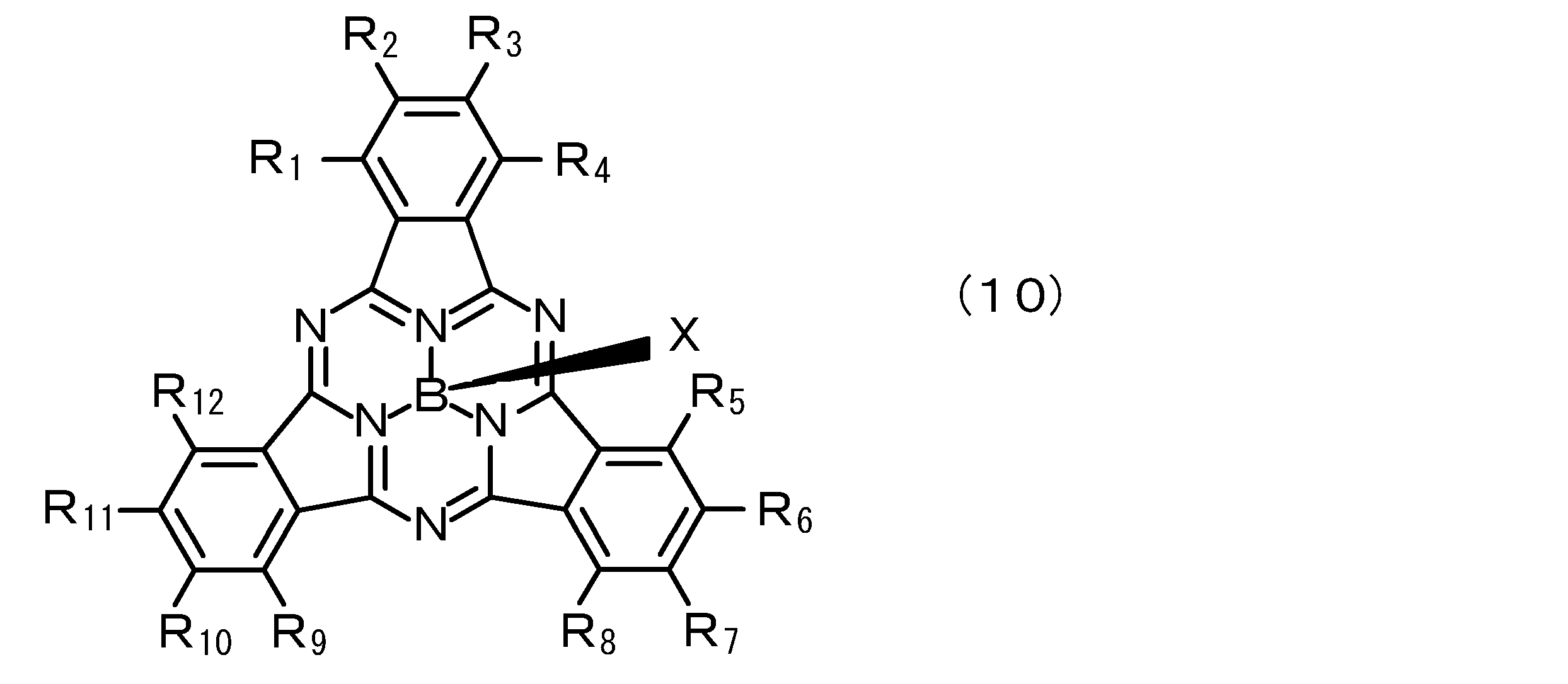
- n型有機半導体材料は、下記の構造式(12)から成る請求項4に記載の撮像素子。

- n型有機半導体材料は、下記の構造式(13)から成る請求項4に記載の撮像素子。

- n型有機半導体材料は、下記の構造式(14)から成る請求項4に記載の撮像素子。
- 第1電極、第2電極、及び、第1電極と第2電極との間に配設された光電変換層を備えており、
光電変換層は、下記の構造式(2)を有するジインデノペリレン誘導体、及び、下記の構造式(14)を有するn型有機半導体材料から成るバルクヘテロ層から構成されている撮像素子。

- 請求項1乃至請求項8のいずれか1項に記載の撮像素子が、1つ、積層されて成る積層型撮像素子。
- 請求項1乃至請求項8のいずれか1項に記載の撮像素子を、複数、備えた固体撮像装置。
- 請求項9に記載の積層型撮像素子を、複数、備えた固体撮像装置。
Applications Claiming Priority (2)
| Application Number | Priority Date | Filing Date | Title |
|---|---|---|---|
| JP2015168695 | 2015-08-28 | ||
| JP2015-168695 | 2015-08-28 |
Publications (1)
| Publication Number | Publication Date |
|---|---|
| WO2017038256A1 true WO2017038256A1 (ja) | 2017-03-09 |
Family
ID=58187100
Family Applications (1)
| Application Number | Title | Priority Date | Filing Date |
|---|---|---|---|
| PCT/JP2016/070637 Ceased WO2017038256A1 (ja) | 2015-08-28 | 2016-07-13 | 撮像素子、積層型撮像素子及び固体撮像装置 |
Country Status (1)
| Country | Link |
|---|---|
| WO (1) | WO2017038256A1 (ja) |
Cited By (2)
| Publication number | Priority date | Publication date | Assignee | Title |
|---|---|---|---|---|
| CN110908029A (zh) * | 2019-11-14 | 2020-03-24 | Tcl华星光电技术有限公司 | 光纯化层、侧入式背光模组及偏光片 |
| CN111448663A (zh) * | 2017-12-05 | 2020-07-24 | 索尼公司 | 摄像元件、层叠型摄像元件和固态摄像装置 |
Citations (3)
| Publication number | Priority date | Publication date | Assignee | Title |
|---|---|---|---|---|
| JP2014082405A (ja) * | 2012-10-18 | 2014-05-08 | Seiko Epson Corp | 発光素子、発光装置、認証装置および電子機器 |
| WO2014073446A1 (ja) * | 2012-11-09 | 2014-05-15 | ソニー株式会社 | 光電変換素子および固体撮像装置ならびに電子機器 |
| US20150188064A1 (en) * | 2014-01-02 | 2015-07-02 | Samsung Electronics Co., Ltd. | Organic photoelectronic device and image sensor |
-
2016
- 2016-07-13 WO PCT/JP2016/070637 patent/WO2017038256A1/ja not_active Ceased
Patent Citations (3)
| Publication number | Priority date | Publication date | Assignee | Title |
|---|---|---|---|---|
| JP2014082405A (ja) * | 2012-10-18 | 2014-05-08 | Seiko Epson Corp | 発光素子、発光装置、認証装置および電子機器 |
| WO2014073446A1 (ja) * | 2012-11-09 | 2014-05-15 | ソニー株式会社 | 光電変換素子および固体撮像装置ならびに電子機器 |
| US20150188064A1 (en) * | 2014-01-02 | 2015-07-02 | Samsung Electronics Co., Ltd. | Organic photoelectronic device and image sensor |
Cited By (3)
| Publication number | Priority date | Publication date | Assignee | Title |
|---|---|---|---|---|
| CN111448663A (zh) * | 2017-12-05 | 2020-07-24 | 索尼公司 | 摄像元件、层叠型摄像元件和固态摄像装置 |
| CN111448663B (zh) * | 2017-12-05 | 2024-04-16 | 索尼公司 | 摄像元件、层叠型摄像元件和固态摄像装置 |
| CN110908029A (zh) * | 2019-11-14 | 2020-03-24 | Tcl华星光电技术有限公司 | 光纯化层、侧入式背光模组及偏光片 |
Similar Documents
| Publication | Publication Date | Title |
|---|---|---|
| JP7586230B2 (ja) | 撮像素子、積層型撮像素子及び撮像装置 | |
| JP7343463B2 (ja) | 撮像素子、積層型撮像素子、及び、固体撮像装置 | |
| JP6834400B2 (ja) | 撮像素子、積層型撮像素子、撮像装置及び電子装置 | |
| JP7033548B2 (ja) | 撮像素子、積層型撮像素子及び撮像装置 | |
| JP6769435B2 (ja) | 光電変換素子、撮像素子、積層型撮像素子及び撮像装置 | |
| WO2018110050A1 (ja) | 光電変換素子、撮像素子、積層型撮像素子及び固体撮像装置 | |
| JP2017005196A (ja) | 固体撮像素子および固体撮像素子の製造方法、光電変換素子、撮像装置、電子機器、並びに光電変換素子。 | |
| JP2020127033A (ja) | 撮像素子及び固体撮像装置 | |
| JP5702074B2 (ja) | 固体撮像装置 | |
| WO2017038256A1 (ja) | 撮像素子、積層型撮像素子及び固体撮像装置 | |
| JP2021093534A (ja) | 撮像素子、積層型撮像素子、撮像装置及び電子装置 |
Legal Events
| Date | Code | Title | Description |
|---|---|---|---|
| 121 | Ep: the epo has been informed by wipo that ep was designated in this application |
Ref document number: 16841288 Country of ref document: EP Kind code of ref document: A1 |
|
| NENP | Non-entry into the national phase |
Ref country code: DE |
|
| 122 | Ep: pct application non-entry in european phase |
Ref document number: 16841288 Country of ref document: EP Kind code of ref document: A1 |
|
| NENP | Non-entry into the national phase |
Ref country code: JP |