WO2017022004A1 - パターン高さ計測方法およびパターン高さ計測装置 - Google Patents
パターン高さ計測方法およびパターン高さ計測装置 Download PDFInfo
- Publication number
- WO2017022004A1 WO2017022004A1 PCT/JP2015/071739 JP2015071739W WO2017022004A1 WO 2017022004 A1 WO2017022004 A1 WO 2017022004A1 JP 2015071739 W JP2015071739 W JP 2015071739W WO 2017022004 A1 WO2017022004 A1 WO 2017022004A1
- Authority
- WO
- WIPO (PCT)
- Prior art keywords
- pattern
- height
- waveform
- sample
- specific intensity
- Prior art date
- Legal status (The legal status is an assumption and is not a legal conclusion. Google has not performed a legal analysis and makes no representation as to the accuracy of the status listed.)
- Ceased
Links
Images









Classifications
-
- G—PHYSICS
- G01—MEASURING; TESTING
- G01B—MEASURING LENGTH, THICKNESS OR SIMILAR LINEAR DIMENSIONS; MEASURING ANGLES; MEASURING AREAS; MEASURING IRREGULARITIES OF SURFACES OR CONTOURS
- G01B11/00—Measuring arrangements characterised by the use of optical techniques
- G01B11/02—Measuring arrangements characterised by the use of optical techniques for measuring length, width or thickness
-
- G—PHYSICS
- G01—MEASURING; TESTING
- G01B—MEASURING LENGTH, THICKNESS OR SIMILAR LINEAR DIMENSIONS; MEASURING ANGLES; MEASURING AREAS; MEASURING IRREGULARITIES OF SURFACES OR CONTOURS
- G01B15/00—Measuring arrangements characterised by the use of electromagnetic waves or particle radiation, e.g. by the use of microwaves, X-rays, gamma rays or electrons
Definitions
- the present invention relates to a pattern measuring method and a pattern height measuring apparatus for measuring the height of a pattern using a charged particle beam apparatus such as an electron microscope, and in particular, measuring the height of a pattern using spectral waveform information.
- the present invention relates to a pattern height measuring method and a pattern height measuring apparatus.
- the pattern has a three-dimensional structure in which a large number of pattern layers are stacked, and patterns having a pattern width and pattern pitch of 20 nm or less have been seen.
- conventional shape inspections such as height
- a scatterometry technique that uses a light source such as a semiconductor laser to irradiate the object to be measured and identifies the pattern shape.
- a light source such as a semiconductor laser
- Patent Document 1 There is a technique disclosed in Patent Document 1 as a prior art example related to the above measuring device.
- Patent Document 1 irradiates light on a target pattern of a substrate on which a pattern is formed, compares a detection waveform formed based on the reflected light with a signal waveform generated by simulation and registered in a library, A shape measurement method for obtaining pattern shape information based on selection of a calculated waveform that is the best match is described. Further, Patent Document 1 describes that when a calculation waveform cannot be selected, a pattern is measured by another measuring device (CD-SEM (Critical Dimension-Scanning Electron Microscope) or the like). Further, Patent Document 2 describes a technique for storing the relationship between the pattern height and image information in advance and obtaining the pattern height using image information obtained by an electron microscope image.
- CD-SEM Cross-Scanning Electron Microscope
- JP 2011-27461 A (corresponding US Pat. No. 8,227,265) JP 2012-173028 A
- Recent semiconductor devices having a three-dimensional structure include a plurality of layers in addition to a layer including a pattern to be measured.
- the detection waveform formed based on reflected light includes a layer that includes a pattern to be measured. It also changes depending on the reflectance, physical properties, or interface of another layer. Therefore, when obtaining the pattern height of a specific layer of a multilayer structure based on reflected light detection, a library corresponding to the type of layer other than the layer that includes the pattern to be measured and combinations of multiple possible layers It is necessary to prepare.
- a library corresponding to various types and combinations of layers has an enormous amount of data, and it is very difficult to construct the library itself. Even if such a library can be prepared, the time required for matching becomes enormous.
- a scanning electron microscope as disclosed in Patent Document 2 is an apparatus that can image a pattern shape at a higher magnification than an optical inspection apparatus or the like.
- an electron microscope is an apparatus that can form a two-dimensional image at a high magnification, it is difficult to obtain information in the height direction (the optical axis direction of the electron beam) from the two-dimensional image.
- a pattern having a height difference for example, a line and space pattern
- the widths of the line and the space are the same, the two may not be distinguished.
- the following proposes a pattern height measurement method and a pattern height measurement device for measuring the height of a pattern included in a specific layer of a multilayer structure at high speed and with high accuracy.
- a pattern height measuring method and apparatus for measuring the height of a pattern formed on a sample based on scanning of a charged particle beam with respect to the sample.
- a first specific intensity that is a specific intensity between a first signal waveform obtained based on dimension information of a pattern obtained by scanning with a charged particle beam and a second signal waveform of a sample on which the pattern is not formed.
- the waveform is obtained, the first specific intensity waveform, the third signal waveform generated based on the reflected light obtained by irradiating the sample on which the pattern is formed, and the sample on which the pattern is not formed
- Matching is performed with a second specific intensity waveform that is a specific intensity with a fourth signal waveform generated based on reflected light obtained by light irradiation on the first specific intensity
- Information on the height of the pattern used to calculate the first signal waveform when the degree of coincidence between the waveform and the second specific intensity waveform is the highest or when the degree of coincidence satisfies a predetermined condition Based on the above, a pattern height measuring method and apparatus for determining the height of the pattern are proposed.
- the pattern height of a specific layer included in the multilayer structure can be measured at high speed and with high accuracy.
- the figure which shows an example of a pattern measurement system The figure which shows the flow of a process of pattern height measurement.
- the flowchart which shows the process of performing the height measurement of a pattern using the output data of a spectrophotometer, and the output data of the scanning electron microscope which can measure the dimension of a pattern.
- the figure which shows an example of the measurement position set on the wafer.
- the figure which shows an example of the composite system of an electron microscope and a pattern height measuring device.
- the flowchart which shows the calibration process of the pattern height measuring apparatus using a calibration sample.
- the figure which shows the outline
- the flowchart which shows the process of calculating
- the flowchart which shows the process of calculating
- the flowchart which shows the process of measuring pattern height based on the matching between a reference specific intensity waveform and a calculated specific intensity waveform.
- the first information obtained by scanning the charged particle beam with respect to the pattern formed on the sample and the second information obtained based on the spectral waveform obtained by irradiating the sample with light are included.
- the present invention relates to a pattern height measuring method and apparatus for measuring the height of a pattern based on the above.
- a measurement method and apparatus that enable yield management in a semiconductor device manufacturing process by applying the semiconductor manufacturing apparatus to in-line measurement will be described in connection with a pattern height measurement method of a semiconductor device having a fine pattern.
- a pattern measuring apparatus using a scatterometry technique a large number of waveform models are stored in advance, and the pattern height is measured based on a comparison between the waveform model and the detected waveform. Since the spectral waveform varies depending on the physical properties and reflectance of the sample, it is necessary to prepare a model according to the type of the sample. Further, when the sample has a multilayer structure, it is necessary to consider not only the pattern of the target layer but also the presence of the lower layer pattern, and thus it is necessary to prepare more models. In addition, when performing in-line measurement of semiconductor devices, it is necessary to prepare multiple measuring devices to improve throughput, but it is also necessary to take into account machine differences between devices, and the conditions for performing high-precision measurement It is extremely difficult to align. From the above situation, it is assumed that an error of about 2 to 10 nm occurs when performing height measurement using a normal scatterometry technique.
- In-line measurement requires both high precision measurement and high measurement throughput.
- a pattern height measuring method and a pattern height measuring apparatus that can selectively measure a pattern to be measured after processing (after pattern formation) and can realize the measurement at high speed and stably. This will be described in detail.
- the effect of the machine difference reduction of a several measuring apparatus can also be anticipated.
- a light source unit that outputs white light having a large number of wavelengths on a pattern surface having a periodic structure, an optical system that irradiates the object to be measured with light from the light source unit, and enters the reflected light, and A spectroscopic detector that divides the reflected light from the object to be measured and detects it as a spectral waveform, an arithmetic unit that calculates the height of the pattern based on the wavelength and intensity results of the spectral waveform, and before the upper management data
- a pattern height measurement system that obtains a pattern height result by using a pattern layer as a measurement target as a single layer by removing the influence of a layer lower than the pattern layer as a measurement target by using a spectral result in the process as a reference waveform.
- a pattern height measurement system having the spectral wavelength and intensity data as well as the data recording the process, measurement device and measurement conditions as the spectral result of the previous process of the reference waveform.
- the spectral waveform of the pattern before the CMP process is spectroscopically measured.
- a condensing lens that condenses the light from the light source onto the measurement object, a measurement light detection lens that forms an image of light on each of the measurement object and the measurement light detection unit, and a pattern direction
- a pattern height measuring system comprising a photometer having a rotation control unit corresponding to the pattern forming direction, the polarizing plate being configured by a rotating stage.
- the wavelength of the light output from the light source unit is, for example, a first wavelength in the range of 300 to 800 nm, or a second wavelength in the range of 1100 to 1600 nm corresponding to the photosensitive resist film,
- the pattern height measurement system can select the wavelength of the light output from the light source unit in accordance with the material to be measured and the spectroscope.
- Movement that moves the object to be measured by mounting the dimension measuring device using charged particles such as an electron microscope that measures the reflected light from the object to be measured and the pattern of the object to be measured, and the pattern height measuring device.
- Height measurement system comprising: a type sample stage; a position measurement unit for measuring the position or movement distance of the movable sample stage; a calibration substrate; and a sample fixing unit.
- the pattern height measuring device irradiates the object to be measured with a light source unit that emits light to a pattern formed on a base material sample, a polarization unit that polarizes light from the light source unit, and light from the light source.
- the incident light that enters the target alignment mark alignment camera and the spectroscope, and the splitting optical system that guides the pattern, and the light that passes through the polarizing plate that irradiates the pattern enters the spectroscope.
- a polarizing plate that can be rotated in front of the spectroscope to identify the polarization direction of the light a rotation angle detection unit that detects the rotation angle of the polarizing plate, and reflected light from the object to be measured as measurement light by the spectroscope Based on the spectral intensity of the measurement light, a specific intensity comparison unit that compares the intensity using the spectral result of the previous process as a reference light signal, and the measurement ratio based on the result of the specific intensity and wavelength Strength and pattern pitch
- the pattern height measurement system includes the mobile sample stage, an alignment mark detection unit, and a spectroscopic measurement unit, and the height calculation unit includes position information, light projection, and a spectroscope of the mobile sample stage.
- the height data in the profile data is recorded together with the position information using the polarization angle of the light incident on.
- the pattern height measurement device has the same measurement conditions as the storage unit for storing data of the measurement object such as the light amount, the spectral waveform, and the height result of the calibration sample for each measurement device. Difference calculation that calculates the relative strength of the profile data of different measurement date and time, compares the difference with the management value, and outputs the result of the comparison And a function for outputting an alarm based on the management value from the difference to the upper management system.
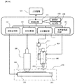
- FIG. 1 is a diagram illustrating an example of a pattern measurement system (pattern height measurement device) in which an electron microscope 200 and a pattern height measurement device 001 are provided.
- the electron microscope 200 generates an image signal or a signal waveform based on detection of a detection signal (secondary electrons or backscattered electrons) obtained by scanning an electron beam, and measures a pattern dimension based on the signal waveform. It is a device that performs. By determining the dimension between the peaks of the waveform profile, for example, the dimension of the line width and pitch of the line and space pattern is measured.
- the movable sample stage 130 has a moving range so that a desired position on the sample can be irradiated with an electron beam by the electron microscope 200 or light by the pattern height measuring device 001.
- the movable sample stage 130 can automatically move to preset coordinates of the movement position, and can control, manage, and record relative movement coordinates.
- a scanning deflection optical device for scanning the electron beam, a focusing lens for focusing the electron beam, electrons emitted from the sample, or electrons emitted from the sample are other members (secondary electron conversion).
- a detector that detects electrons generated by colliding with an electrode, etc., and an arithmetic unit that generates an image signal and a signal waveform based on a signal detected by the detector and performs pattern dimension measurement It has been.
- the pattern height measuring device 001 is provided with a CCD (Charge Coupled Device) camera 031.
- the electron microscope 200 has an observation magnification of 100 times or more, and its field of view (Field Of View: FOV) is very small. Therefore, it is difficult to position a pattern or the like to be measured directly in the field of view on the movable sample stage 130. Therefore, the height measuring device 001 performs rough alignment using an alignment mark or the like created on the sample substrate.
- the pattern height measuring device 001 also functions as a low magnification optical microscope.
- the pattern height measuring device 001 functions as an optical microscope and a spectroscope that divides the reflected light.
- the illumination light source 010 for example, an LED (Light Emitting Diode) light source capable of emitting visible light having a wavelength of about 300 to 800 nm can be used.
- the pattern height measuring device 001 includes a condensing lens A012 for efficiently illuminating the light emitted from the illumination light source 010, a rotatable polarizing plate A020, and coaxial with the light receiving system to correspond to the pattern direction of the device.
- a half mirror 024, a light receiving system condenser lens B013, and a microscope objective lens 023 for irradiating light onto the wafer 002 are provided so as to be incident on the light projecting optical axis.
- the reflected light from the sample passes through the reverse route, passes through the microscope objective lens 023, the light receiving system condenser lens B013, and the half mirror 024, and is condensed on the imaging surface of the CCD camera 031.
- a low-magnification image can be acquired based on the output signal of the CCD camera 031.
- a branching prism 014 and a mirror 032 for branching at a predetermined light quantity ratio are installed in front of the CCD camera 031 on the spectroscope 011 side, and through a rotatable polarizing plate B021 for separating the horizontal and vertical components of the polarization axis.
- the light is guided to the spectroscope optical fiber 022.
- a signal from the spectroscope 011 is stored in a storage medium or the like as light intensity for each wavelength, and can be output as a spectral waveform (spectral waveform) by an arithmetic device or the like (not shown).
- an LED light source is exemplified as the illumination light source 010
- an LD Laser Diode
- a halogen lamp or an SLD (Super Luminescent Diode)
- a CMOS camera may be used instead of the CCD camera.
- FIG. 1 an example in which light is guided to a spectroscope using an optical fiber has been described, but a diffraction grating or a prism may be arranged so that light is detected directly by a line CCD or the like after spectroscopy. Good.
- the pattern height measuring device 001 can be used by exchanging an optical microscope for alignment mark confirmation in an existing electron microscope.
- FIG. 2 is a diagram showing a rough flow of the pattern height measurement method in this embodiment.
- the wafer 002 on which the pattern is formed in the semiconductor manufacturing process is taken out from the FOUP or the like, which is a wafer storage container, by a robot or the like and mounted on the movable sample stage 130.
- the optical microscope 034 confirms the alignment mark on the wafer 002, moves to a predetermined position with the movable sample stage 130, and measures the width and pitch of the linear pattern with the electron microscope. Next, the spectral waveform by the reflected light shown in the figure is measured, and the pattern height is measured.
- the pattern width and pattern pitch have been narrowed, and are 1/10 times or less compared to the wavelength of the light source used in the optical microscope. Therefore, it is difficult to visualize a fine pattern with an optical microscope.
- the height of the pattern can be measured by treating it as a film in which the medium in the range observed with the optical microscope and the material constituting the pattern formed in the range are homogeneously mixed.
- an effective medium approximation method is used to measure the height of the film. The height measurement principle based on the effective medium approximation will be described below.
- Effective medium approximation formula In the effective medium approximation, it is possible to calculate the reflectance from the volume ratio in an object having a pitch or width less than the wavelength of light.
- the target film is assumed to be a uniform material, height dimension and volume in the light irradiation range, and is obtained by the following equation. Since it depends on the pattern direction, the calculation formula differs depending on the TM and TE deflection directions.
- the refractive index of the material is known by prior measurement using an ellipsometer or the like. Therefore, in the effective medium approximation of the present embodiment, the wavelength ⁇ and the pattern are measured based on the pattern pitch and width dimension values by the measurement function of the electron microscope 200. It is possible to calculate the spectral waveform of the reflected light with respect to the layer height d.
- the parameters are reduced, and this waveform and volume ratio effect Waveform calculation for fitting a waveform change from a height reference waveform is performed by the spectrometer control unit 111, and the optimum waveform fitting 112 for the height change is taken, thereby obtaining the height d113 without using a library. it can.
- this waveform is calculated in advance by RCWA (Rigorous Coupled Wave Analysis), etc., and stored as a library, so that matching is performed based on the pitch and width dimensions obtained by the scanning electron microscope 200.
- the height d to be obtained can also be obtained.
- height measurement can be performed without preparing a library, so that high-precision measurement can be realized more easily.
- the spectral waveform in the lower layer of the layer including the pattern to be measured (the spectral waveform acquired before the pattern layer is formed) is used as the reference waveform, and the reference waveform and the pattern are By performing the calculation using the specific intensity waveform obtained based on the comparison with the spectral waveform obtained after being formed, it is possible to suppress the number of parameters used for the height measurement calculation.
- FIG. 3 is a diagram illustrating an example in which the spectral waveform Bg ( ⁇ ) 091 of the low reflection sample (low reflection sample 035) is acquired by the pattern height measuring device 001 illustrated in FIG.
- the spectral waveform Bg ( ⁇ ) is a background signal of the measuring device, and is used for calibration that is performed before or periodically.
- the spectral waveform 091 is used in the reflectance calculation formula for each wavelength shown in FIG.
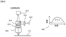
- FIG. 4 is a diagram illustrating an example of acquiring a spectral waveform Rf ( ⁇ ) (reference waveform) 092 of a sample (a pre-process pattern sample 036) before a pattern to be height measurement described later is formed.
- Spectral waveform data is managed by a host data management system based on the lot number and coordinates, or stored in association with identification information in a storage medium (not shown) so that it can be read out as necessary.
- This spectral waveform 092 is used to calculate the reflectance for each wavelength shown in FIG. FIG.
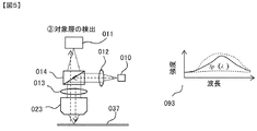
- FIG. 5 is a diagram showing an example in which a spectral waveform Sp ( ⁇ ) 093 of a sample (target process pattern sample 037) on which a pattern to be measured is formed is acquired.
- the spectral waveform data is also managed by the host data management system together with the measurement device information, measurement conditions, lot number, coordinates, and the like.
- the spectral waveform 093 is used for calculating the reflectance for each wavelength shown in FIG.
- FIG. 6 is a diagram showing an example in which the specific reflectance waveform R ( ⁇ ) (specific intensity waveform) 094 is obtained using the specific intensity calculation formula 095.
- This spectral waveform data is also recorded and managed by the host data management system together with information on the measuring device used, measurement conditions, lot numbers, coordinates, and the like. Pattern height measurement is executed based on the specific intensity waveform obtained here and the pattern dimension information obtained by the electron microscope. Details will be described later.
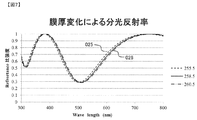
- FIG. 7 is a diagram showing an example of a spectral waveform obtained by irradiating light to samples having different film thicknesses.
- the base material is silicon
- the thickness of the single layer film of SiO 2 is 255. .5nm waveform 025), specific intensity waveform obtained at 258.5nm and 260.5nm (waveform 026).
- the waveform can be obtained not only from a spectrophotometer but also from an effective medium approximation formula in which the width and pitch of the pattern are added.
- Matching is performed between the calculated specific intensity waveform obtained by changing the height d in Equations 9 and 10 and the specific intensity waveform generated based on the spectral waveform acquisition before and after pattern formation by the spectrophotometer.
- the height d inputted to obtain the calculated specific intensity waveform having the highest degree of coincidence can be obtained as the pattern height. Further, when the degree of coincidence is a predetermined value or more, the height d used for the calculation of the calculated specific intensity waveform may be set as the pattern height.
- FIG. 8 is a diagram showing an outline of a library in which the reflectance of the material, the pattern width, and the pattern pitch are used as the library tag. Based on these conditions, the film height is calculated as a parameter, and the result is stored and managed as a library. Using this result, the best matching waveform is selected and the pattern height is obtained.
- FIG. 9 and 10 are diagrams for explaining the state of reflected light in accordance with the layer stacking state.
- FIG. 9 shows a sample in which a first layer pattern film 053 is laminated on a wafer 051 serving as a base material, and a sample in which a second layer pattern 054 is further laminated on the first layer pattern film 053. Illustrated.
- illumination light 082 reflected light 083 reflected at the boundary surface of the first layer is obtained.
- spectral waveform obtained when the sample is irradiated with light in the state in which the first pattern film 053 is formed and before the second pattern film 054 is formed.
- the specific intensity waveform as described above can be obtained by setting the waveform as a detection waveform and the spectral waveform obtained after the second layer pattern film 054 is formed.
- FIG. 10 illustrates a sample in which the first layer pattern film 053 and the second layer pattern film 054 are formed, and a sample in which the third layer pattern film 055 is further laminated on the second layer pattern film 054.
- a reference waveform is generated using the reflected light 083 obtained by irradiating the sample with the second layer pattern 054 as the uppermost layer, and the sample having the third layer pattern film 055 is irradiated with light.
- a specific intensity waveform for measuring the height of the third layer pattern film 055 can be generated.
- FIG. 11 is a flowchart showing a process of performing pattern height measurement using output data of the spectrophotometer and output data of a scanning electron microscope capable of measuring the dimension of the pattern.
- the following control is executed by supplying a predetermined signal to each component from a control device that controls the scanning electron microscope.
- step 1100 the semiconductor wafer after the film forming process or the etching process is taken out from the transfer container (FOUP, SMIF pod, etc.) with a robot, a transfer jig, etc., and placed on the movable sample stage 130. Wafer information such as the lot number and process number is managed in the measurement process by a higher order communication input command.
- the transfer container FOUP, SMIF pod, etc.
- step 1101 the movable sample stage 130 is moved and positioned based on the measurement position information.
- step 1102 further precise positioning is performed based on the alignment mark information.
- step 1103 the movable sample stage 130 is moved to position the pattern that is the height measurement target in the field of view of the electron microscope 200.
- step 1104 the pattern width (w) and pitch (p) are measured using the electron microscope 200.
- a dummy sample for height measurement is formed away from the original measurement position by the distance between the optical axis of the electron microscope 200 and the optical axis of the pattern height measuring device 001, thereby moving the movable sample. It is possible to move to the next step 1106 without performing the movement using the table 130 (step 1105).
- step 1106 the spectral waveform of the sample is acquired using the pattern height measuring device 001.
- step 1105 all spectroscopic measurements at the measurement positions registered in advance in the imaging recipe or the like are performed, and in step 1108, the result of the previous process of the wafer (reference waveform) is read from the upper management unit to obtain a specific intensity waveform.
- step 1109 the pattern height is calculated based on the spectral waveforms obtained at a plurality of locations, the pattern width, and the pitch. Based on this result, in step 1110, the pattern height abnormality (process abnormality in the machining process) is determined using the threshold value assigned for each process. Here, for example, it is determined whether an abnormality has occurred at a plurality of points, or whether an abnormality has occurred continuously on different wafers, etc., and an abnormality in the process is detected.
- step 1111 by confirming whether remeasurement or cause investigation is necessary, in step 1112, it is possible to notify the upper management apparatus of a line abnormality at an early stage.
- step 1113 the substrate is unloaded and the next substrate (wafer) is awaited for loading.
- pattern dimension measurement and spectroscopic measurement using the electron microscope 200 are performed in series, but the measurements may be performed in combination.
- FIG. 20 is a flowchart showing a process for obtaining a calculated specific intensity waveform of the pattern height d based on pattern width and pitch measurement by a scanning electron microscope.
- the pattern width w and the pitch p are measured by electron beam scanning with respect to the region where the pattern is formed (step 2001).
- the volume ratio coefficient f is calculated by substituting w and p into the above-described equation 2 (step 2002).
- such an arithmetic expression is stored in advance in a storage medium such as a predetermined arithmetic apparatus, and the arithmetic processing is automatically executed based on the measurement by the scanning electron microscope.
- parameters such as the refractive index N are read based on information such as the type of material selected in advance, and the reflectance R is calculated using equations 9 and 10 based on the settings of the height d and the wavelength ⁇ . Calculation is performed (step 2003 to step 2005).
- the calculation of the reflectance R in step 2005 is performed for the wavelengths ⁇ 1 to ⁇ m , and the calculated spectral waveform Spc ( ⁇ 1 to ⁇ m ) (first signal waveform) is obtained based on the calculation of the reflectance R ( Step 2006).
- a signal waveform reference spectral waveform (second signal waveform)
- second signal waveform reference spectral waveform
- a calculated specific intensity waveform Spc ( ⁇ 1 to ⁇ m ) (first specific intensity waveform)
- Spc first specific intensity waveform
- a matching process is performed between the calculated specific intensity obtained in this way and the measured specific intensity (second specific intensity waveform) (step 2009). If the coincidence or difference is not within the specified range, the pattern height value is changed. (+ ⁇ d) (step 2010).
- the measurement specific intensity is obtained from the spectral waveforms before and after the formation of the pattern to be measured.
- the calculated specific strength is matched with the measured specific strength, and if the calculated specific strength matches or is within the regulation, it is registered in a predetermined storage medium (step 2011).
- the parameter d which is information used to obtain the calculated spectral waveform Spc ( ⁇ 1 to ⁇ m ) when matching is established, is the pattern height, and the numerical information d is output to a display device or the like (not shown).
- the user of the measuring device can know the height of the pattern.
- the numerical value of d may be a parameter that changes according to a change in height, instead of the height, and the pattern height may be output by multiplying the parameter by a predetermined coefficient.
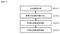
- FIG. 21 is a flowchart showing a process for obtaining a specific intensity waveform based on spectral waveform detection by the pattern height measuring device 001.
- a spectral waveform is detected based on the reflected light detection (step 2101).
- the reference spectral waveform is read (step 2102).
- the reference spectral waveform is a spectral waveform acquired based on light irradiation on the sample before the formation of the measurement target pattern, and this spectral waveform is read as a reference spectral waveform.
- a measurement specific intensity waveform is obtained by multiplication or division between the reference spectral waveform read in this way and the spectral waveform acquired after the measurement target pattern is formed, and the information is stored in a predetermined storage medium. Registration is performed (steps 2103 and 2104).
- FIG. 22 is a flowchart showing a process of measuring the pattern height based on matching (fitting) between the measured specific intensity waveform and a plurality of calculated specific intensity waveforms.
- the measured specific intensity waveform and a plurality of calculated specific intensity waveforms stored in association with the height d are read out and matching is performed between them (steps 2201 to 2203).
- a calculated specific intensity waveform that most closely matches the measured specific intensity waveform, or a calculated specific intensity waveform having a matching degree equal to or higher than a predetermined value is selected, and the height d stored in association with the calculated specific intensity waveform is patterned.
- the height is output (step 2204).
- FIG. 12 is a diagram illustrating an example of measurement positions set on the wafer.
- the wafer lot information, the conditions of the optical microscope associated with the wafer lot information, the information on the previous process, and the measurement position information are sent to the control unit. Based on this information, the movable sample stage 130 is moved and positioned, and further precise positioning is performed based on the alignment mark information.
- the movable sample stage 130 is moved so that the measurement target pattern is positioned at a measurement position set in advance in an imaging recipe or the like, and the width and pitch of the pattern at the pattern surface measurement position 073 are measured by the electron microscope 200, for example.
- the measurement position 073 of the wafer 080 generated in the pattern manufacturing process A is measured by the scanning electron microscope and the spectral waveform is acquired by the spectrophotometer, and is generated by the pattern manufacturing process B which is a subsequent process of the pattern manufacturing process A.
- the same measurement is performed on the same measurement position 073 of the wafer 081.
- the height of the pattern generated in the pattern step A is obtained by performing the spectroscopic measurement at the set position and reading out the spectroscopic measurement result in the previous step of the wafer 080 generated in the pattern step A from the upper management unit. It is possible to obtain a specific intensity waveform for obtaining.
- the pattern dimension measurement and the spectroscopic measurement by the electron microscope 200 may be performed in series, or the pattern dimension measurement and the spectroscopic measurement of the electron microscope 200 may be performed in combination.
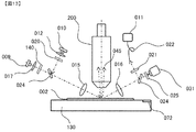
- FIG. 13 shows an example of a combined system of an electron microscope and a pattern height measuring device in which the irradiation position of the electron beam of the electron microscope 200 and the irradiation position of light emitted from the irradiation light source 010 of the pattern height measuring device are matched.
- the pattern height measuring apparatus in FIG. 13 can measure the height of the irradiation position of the electron beam
- the focal position of the electron microscope 200 can be adjusted based on the obtained height information.
- the autofocus control can be performed by adjusting the excitation condition of the objective lens of the electron microscope in accordance with the height measurement information by the pattern height measuring device.
- the sample height can be measured based on a fitting process using a calculated spectral waveform obtained based on [Equation 9], [Equation 10] and the like.
- An LD, LED, halogen lamp, SLD, or the like is used for the illumination light source 010 of the pattern height measuring apparatus illustrated in FIG. 13, and the coaxial incident optical system illustrated in FIG.
- the structure is divided into optical systems.
- the projection image of the slit 140 may be received by the CCD 031 and the height may be measured based on the position information of the projection image of the slit.
- the projection optical system has two light sources with different wavelengths.
- the light emitted from the two light sources (09, 10) is configured to pass through the same optical axis by the half mirror 024 via the condenser lenses 017, 012.
- the light passing through the half mirror 024 is imaged on the surface of the wafer 002 by the condenser lens 015, and the reflected light passes through the condenser lens 016 and the branching prism 024, and is an optical fiber connected to the imaging surface of the CCD 031 and the spectroscope 011. 022.
- a drive mechanism for driving the slit pattern 140 or the half mirror 024 is provided so as to be switched between the focus control of the electron microscope and the spectroscopic measurement. good.
- the light source may be turned on and off according to the application to be used. In this configuration, the light projecting side to be used can be made common, and a one light source configuration can be provided, so that an inexpensive system can be provided. At this time, a rotating polarizing plate B021 is disposed in front of the optical fiber 022 entrance on the light receiving side.
- FIGS. 14 to 16 are diagrams for explaining a measurement system including a plurality of measurement devices and a technique for suppressing a machine difference between the plurality of measurement devices.
- FIG. 14 is a diagram showing an outline of a measurement system including three electron microscopes (measuring machine A 1012, measuring machine B 1022, and measuring machine C 1032).
- a measuring device A 1012, a measuring device B 1022, and a measuring device C 1032 are connected to a control device A 1011, a control device B 1021, and a control device C 1031 that execute respective controls and arithmetic processing based on detection of secondary electrons, reflected light, and the like. ing.
- These control devices are connected to the upper management device 120.
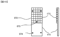
- FIG. 15 is a diagram showing an outline of the calibration chip 072 mounted on the movable sample stage 103.
- the left figure is a top view (figure seen from the electron beam irradiation direction), and the right figure is a side view.
- the calibration chip 072 is provided for each measuring machine, and is used for start-up inspection and periodic inspection. And it is mainly used for abnormality detection and calibration of light quantity and height results.
- the base material is a mirror surface and is the same silicon wafer as the semiconductor device.
- a pattern layer is formed on the base material.
- the pattern layer is made of a material having a known refractive index, and a pattern is formed with a known pattern width, pattern pitch, and height.
- the calibration chip 072 is a cut sample of the wafer. Therefore, for example, a plurality of calibration chips are created on one wafer, and each calibration chip is mounted on the movable sample stage 130 of a plurality of different measuring devices, thereby creating a calibration chip created under the same manufacturing conditions. Calibration of the equipment using the operation chip can be performed.
- the calibration chip 072 By installing the calibration chip 072 on the movable sample stage 130, it is possible to check the change of the apparatus state before the start of each apparatus.
- the sample base material measurement position 076 where the reflectance of the calibration chip 072 is high the light amount of the light source unit is evaluated to confirm the light amount reduction of the light source and adjust the light amount. Further, by using the reflected light obtained by irradiating the pattern surface measurement position 073 with light, the rotation angle of the polarizing plate and the spectral waveform are evaluated, and the evaluation result is compared with the previous evaluation result to obtain a system. A check can be made.
- the specific intensity is calculated by using the spectral waveform at the sample base material measurement position 074 as a reference waveform, and the height result is obtained. By comparing the registered pattern height, the measurement error of the apparatus can be evaluated.
- a reference specific intensity waveform corresponding to known height information for example, 100 nm
- a statistical value of deviation for each wavelength of the specific intensity waveform obtained by measurement are obtained by the height deviation obtained by the calibration reference pattern. It is given as a quantity coefficient.
- a correct height should be obtained by substituting it into a relational expression or the like stored in advance (an error in height normalized by measurement of a number of known samples).
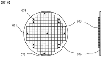
- FIG. 16 is a diagram showing an outline of the calibration wafer 071.
- the plane of the pattern is shown on the left, and the side is shown on the right.
- the calibration wafer 071 is used for abnormality detection and calibration of light quantity and height results for the purpose of starting work inspection, periodic inspection, and periodic inspection between apparatuses.
- the base material is a mirror surface, the same silicon material as the semiconductor device, and a single layer film on which a pattern is formed with typical width, pattern pitch, height, material, and cut out It is.
- the calibration wafer 071 can be stored in a storage container called a hoop.
- the calibration wafer 071 confirms the light amount reduction of the light source unit and adjusts the light amount at the sample base material measurement position 074 having a high reflectivity.
- the rotation angle and the spectral intensity of the polarizing plate at the pattern surface are measured.
- the specific waveform is calculated using the spectral waveform at the sample base material measurement position 074 as a reference waveform, and the measurement result is checked before starting work by calculating the height result. This makes it possible to detect measurement abnormalities.
- Stored in a storage container and by measuring in common to each measuring device, the results between the measuring devices can be compared, and the machine difference can be adjusted to a minimum.
- FIG. 17 is a diagram for explaining a method of suppressing machine differences in the pattern height measuring apparatus using the calibration sample.
- the calibration wafer 071 or the calibration chip 072 is collectively expressed as a calibration sample.
- the calibration wafer 071 or the calibration chip 072 is used for detection of abnormalities in the light quantity and height results, and for checking the difference between the calibration and the apparatus for the purpose of starting inspection and periodic inspection.
- the calibration wafer 071 is stored in the storage container 077, and transported and measured in common for each measuring device, whereby the measurement results between the devices can be compared and the instrumental error can be adjusted to be minimized.
- the calibration chip 072 can be used on a movable sample stage 130 for measurement on a movable sample stage 130 before daily start of the apparatus or for periodic inspection.
- the calibration wafer is managed with a small number of sheets, used for checking instrument differences between apparatuses, and using a calibration chip 072 for pre-start inspection and periodic inspection for each measuring apparatus, thereby waiting time. Therefore, it is possible to manage with a small instrumental difference in the measuring device group.
- These calibration samples are used for checking the light amount reduction and adjusting the light amount of the light source unit at the sample base material measurement position 074 with high reflectance, and at the pattern surface measurement position 073, the rotation angle and spectral intensity of the polarizing plate on the pattern surface.
- the specific waveform is calculated using the spectral waveform at the sample base material measurement position 074 as a reference waveform, and the measurement result is checked before starting work by calculating the height result. This makes it possible to detect measurement abnormalities.
- the calibration sample since the calibration sample is used for confirmation of measurement results, it may be a multilayer film.
- the base material is not limited to silicon, but may be other materials as long as it is close to the product and the physical properties of reflectance are measured in advance.
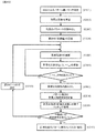
- FIG. 18 is a flowchart showing the calibration process of the pattern height measuring apparatus using the calibration sample.
- step 1200 the calibration wafer stored in the storage container 077 is taken out of the storage container 077 and mounted on the mobile sample stage 130 for periodic confirmation.
- Management information such as the lot number of calibration wafers and previous measurement result information and measurement position information are managed by the host management device, and the measurement device and the control device that controls the measurement device according to the periodic confirmation processing command Sent.
- the movable sample stage 130 moves and positions in step 1201, and in step 1202, further precise positioning is performed based on the alignment mark information.
- step 1203 the sample stage is moved to the pattern measurement position (field position of the electron microscope), and in step 1204, the width and pattern pitch of the pattern are measured with the electron microscope 200. Further, by measuring the dummy pattern portion at the measurement position for height measurement in the sample, the spectral waveform measurement may be performed without moving.
- step 1206 the spectral waveform of the pattern is measured.
- step 1205 all of the spectroscopic measurements at the set positions are performed, and in step 1208, the obtained spectroscopic waveform data and specific intensity at each pattern measurement position are obtained from the reflection spectral waveform of the base material.
- step 1209 these are collectively processed to obtain the film height.
- an abnormality of the measurement apparatus is determined by a threshold, and for example, it is determined whether an abnormality at a plurality of points or an abnormality for each wafer is continued, thereby reducing illumination illuminance or calibration.
- An abnormality such as contamination of the sample for the measurement is detected, the abnormality of the measuring device is notified to the upper management at an early stage, and in step 1211, abnormality processing is performed to determine whether the light amount adjustment is necessary, such as re-measurement or automatic adjustment of illuminance
- the line abnormality can be notified to the upper management at an early stage.
- step 1213 the calibration sample is unloaded and the next substrate loading is awaited.
- pattern dimension measurement and spectroscopic measurement using the electron microscope 200 are performed in series, but each measurement may be combined.
- FIG. 19 is a diagram illustrating an outline of a control device of the pattern height measuring device.
- the upper management apparatus 120 is a part that controls the entire apparatus, and performs input and discharge of samples to and from the measurement apparatus, management of measurement results, management of abnormalities, and the like.
- the upper management apparatus 120 includes, for example, a CPU, RAM, ROM, input device, output device, communication interface, bus, power supply unit, storage unit, and the like.
- the control supervision unit 121 is responsible for communication with the upper management apparatus 120, an electron microscope control 201 that controls the scanning electron microscope 200 system, a sample stage control 131 that controls movement of the movable sample stage 130, and an optical microscope 500.
- the optical microscope control 401 and the spectroscope control system 300 are controlled.
- the control control unit 121 also includes a CPU, RAM, ROM, input device, output device, communication interface, bus, power supply unit, storage unit, and the like. Further, the control supervision unit 121 accepts not only a command from the upper management apparatus 120 but also a setting input by a user's direct operation.
- control control unit 121 has a function of outputting position movement, spectral measurement, height dimension calculation, and each data stored in the storage unit 160 based on a user operation.
- Each part is controlled on the basis of a command from the control control unit 121, and an electron microscope control unit 201 that controls irradiation of an electron beam and detection of secondary electrons in the electron microscope barrel 200, a movable sample base, respectively.
- Each part is controlled by a sample stage controller 131 that controls the movement and positioning of 130, an optical microscope controller 401 that controls an optical system for detecting alignment marks, and a spectrometer controller 111 that controls the spectrometer 011.
- These control units also include a CPU, RAM, ROM, input device, output device, communication interface, bus, power supply unit, storage unit, and the like.
- the storage unit 160 stores data such as spectral waveform data, light amount profile data, light amount control data, spectral results and measurement coordinates. Each of these data is organized and stored as time series data that is data on the time axis such as measurement date and time corresponding to different measurement dates and times.
- pattern forming step B 082 ... illumination light, 083 ... reflected light, 091 ... Background spectral waveform data, 092 ... Reference spectral waveform data, 093 ... Target spectral waveform data, 094 ... Specific intensity spectral waveform data, 095 ... Specific intensity arithmetic expression, 100 ... Pattern height measuring device, 110 ... Control unit, 111 ... spectrometer control unit, 112 ... waveform fitting, 113 ... pattern 114 ... height determination method, 120 ... upper management apparatus, 121 ... control supervision part, 130 ... mobile sample stage, 131 ... sample stage control part, 140 ... vacuum chamber, 141 ... optical window, 150 ... output part DESCRIPTION OF SYMBOLS 160 ...
Landscapes
- Physics & Mathematics (AREA)
- General Physics & Mathematics (AREA)
- Electromagnetism (AREA)
- Length Measuring Devices By Optical Means (AREA)
- Testing Or Measuring Of Semiconductors Or The Like (AREA)
- Length-Measuring Devices Using Wave Or Particle Radiation (AREA)
Abstract
本発明は、多層構造体の特定レイヤに含まれるパターンの高さを高速且つ高精度に計測することが可能とするパターン高さ計測方法及び装置の提供を目的とする。本発明では、荷電粒子ビームの走査によって得られたパターンの寸法情報に基づいて求められる第1の信号波形と、パターンが形成されていない試料の第2の信号波形との比強度である第1の比強度波形と、反射光検出に基づいて求められる第2の比強度波形との間でマッチングを実行し、マッチングが成立したときの第1の信号波形を求めるために用いた高さ情報をパターン高さとするパターン高さ計測方法、及び装置を提案する。
Description
本発明は、電子顕微鏡などの荷電粒子線装置を用いて、パターンの高さを測定するパターン計測方法、およびパターン高さ計測装置に係り、特に分光波形情報を用いて、パターンの高さを測定するパターン高さ計測方法、およびパターン高さ計測装置に関する。
半導体デバイスは、年々微細化とともに立体化が進んでいる。パターンは、多数段のパターン層を積み上げた立体構造となってきており、パターン幅、パターンピッチともに20nm以下のものが見られるようになってきた。また、従来の高さなどの形状検査においては半導体レーザ等の光源を用いて被計測物に照射しパターン形状を特定するスキャットロメトリの技術があるが、パラメータが多く形状決定までに時間がかかる。
上記計測装置に関する先行技術例として、特許文献1に開示の手法がある。特許文献1には、パターンが形成された基板の対象パターンに光を照射し、その反射光に基づいて形成される検出波形と、シミュレーションによって生成され、ライブラリに登録された信号波形を比較し、ベストマッチとなる計算波形の選択に基づいて、パターンの形状情報を求める形状測定法が説明されている。更に特許文献1には、計算波形の選択が不可能な場合に、他計測装置(CD-SEM(Critical Dimension-Scanning Electron Microscope)等)によってパターンを計測することが説明されている。更に、特許文献2には、パターン高さと画像情報との関連を予め記憶しておき、電子顕微鏡像によって得られた画像情報を用いて、パターン高さを求める手法が説明されている。
昨今の立体構造化した半導体デバイスには測定対象となるパターンが含まれるレイヤ以外にも複数のレイヤが含まれている。特許文献1に開示されている反射光の検出に基づいて検出波形を形成し、ライブラリ比較を行う手法の場合、反射光に基づいて形成される検出波形は、測定対象となるパターンが含まれるレイヤとは別のレイヤの反射率、物性値、或いは界面等によっても変化する。よって、多層構造体の特定レイヤのパターンの高さを反射光検出に基づいて求める場合、測定対象となるパターンが含まれるレイヤ以外のレイヤの種類や、複数考えられるレイヤの組み合わせに応じたライブラリを用意する必要がある。このように種々考えられるレイヤの種類や組み合わせに応じたライブラリはデータ量が膨大になり、ライブラリを構築すること自体、非常に困難である。また、仮にこのようなライブラリを用意することができたとしても、マッチングに要する時間も膨大なものとなる。
特許文献2に開示されているような走査電子顕微鏡は、光学式の検査装置等と比較すると高い倍率で、パターンの形状を画像化できる装置である。しかしながら電子顕微鏡は高倍率で2次元画像を形成することができる装置である反面、2次元画像から高さ方向(電子ビームの光軸方向)の情報を得ることは困難である。例えば、高低差があるパターン(例えばラインアンドスペースパターン)の場合、ラインとスペースの幅が同じであると、両者の見分けがつかないことがある。このように、光学式の検査装置と比較して、高さ方向の情報を正確に取得することが困難な走査電子顕微鏡によって得られる情報に基づいて、高精度な高さ測定を行うことは困難である。
以下に、多層構造体の特定レイヤに含まれるパターンの高さを高速且つ高精度に計測することを目的とするパターン高さ計測方法、及びパターン高さ計測装置を提案する。
上記目的を達成するための一態様として、以下に試料に対する荷電粒子ビームの走査に基づいて、試料上に形成されたパターンの高さを計測するパターン高さ計測方法、及び装置であって、前記荷電粒子ビームの走査によって得られたパターンの寸法情報に基づいて求められる第1の信号波形と、前記パターンが形成されていない試料の第2の信号波形との比強度である第1の比強度波形を求め、当該第1の比強度波形と、前記パターンが形成された試料に対する光の照射によって得られる反射光に基づいて生成される第3の信号波形と、前記パターンが形成されていない試料に対する光の照射によって得られる反射光に基づいて生成される第4の信号波形との比強度である第2の比強度波形との間でマッチングを実行し、前記第1の比強度波形と前記第2の比強度波形との一致度が最も高い、或いは当該一致度が所定の条件を満たす場合における前記第1の信号波形を算出するために用いられた前記パターンの高さに関する情報に基づいて、前記パターンの高さを求めるパターン高さ計測方法、及び装置を提案する。
上記構成によれば、多層構造体に含まれる特定レイヤのパターン高さを高速且つ高精度に測定することが可能となる。
以下に説明する実施例は、試料上に形成されたパターンに対する荷電粒子ビームの走査によって得られる第1の情報と、試料に対する光の照射によって得られる分光波形に基づいて得られる第2の情報に基づいて、パターンの高さを測定するパターン高さ計測方法、及び装置に関するものである。特に、微細パターンを有する半導体デバイスのパターン高さ計測法に係り、半導体製造装置のインライン計測への適用によって、半導体デバイスの製造工程での歩留まり管理を可能とする計測法、及び装置を説明する。
スキャトロメトリ技術を用いたパターン測定装置では、予め多数の波形モデルを記憶しておき、この波形モデルと検出波形の比較に基づいて、パターン高さを測定する。分光波形は試料の物性や反射率等によって変化するため、試料の種類に応じてモデルを用意しておく必要がある。また、試料が多層構造となると、目的とするレイヤのパターンだけではなく、下層パターンの存在をも考慮する必要があるため、更に多くのモデルを用意する必要がある。また、半導体デバイスのインライン測定を行う場合、スループット向上のために、測定装置を複数台用意する必要があるが、装置間の機差も考慮する必要があり、高精度測定を行うための条件を揃えることが極めて難しい。上述のような事情から、通常のスキャトロメトリ技術を用いた高さ測定を行う場合、2~10nm程度の誤差が発生すると想定される。
インライン計測では、高精度測定と測定の高スループット化の両立が求められる。以下に、加工後(パターン形成後)に、測定対象となるパターンを選択的に計測対象とすると共に、その計測を高速、且つ安定に実現し得るパターン高さ計測方法およびパターン高さ計測装置について、詳細に説明する。なお、以下に説明する実施例によれば、複数台の計測装置の機差低減の効果も期待できる。
以下に説明する実施例では、主に電子顕微鏡に代表される荷電粒子線装置を含む微細パターンの高さ計測システムであって、以下に示す構成を備えたシステム例について説明する。
(1)周期構造を有するパターン面に多数の波長を有する白色光を出力する光源部と、前記光源部からの光を被計測物に対して照射しその反射光を入射する光学系と、前記被計測物からの反射光を分光し、分光波形として検出する分光検出部と、前記分光波形の波長と強度の結果に基づいて前記パターンの高さを算出する演算部と、上位管理データの前工程での分光結果を参照波形として用いることによって、計測目的とするパターン層より下層の影響を除き、計測目的とするパターン層を単層としてパターン高さ結果を得るパターン高さ計測システム。
(2)前記、参照波形の前工程の分光結果として、分光波長、強度データとともに、工程および計測装置と計測条件を記録したデータを有するパターン高さ計測システム。例えば、パターンの最終平坦化加工工程で、CMP(Chemical Mechanical Polishing)加工工程後のパターン高さを測定したい場合、CMP加工工程前のパターンの分光波形を分光計測しておき、CMP加工工程後の分光波形データと前工程のパターン形成前の分光波形データの比強度を得ることにより、目的とする工程のパターン高さを見ることが容易になる。
(3)光源からの光を前記被計測物に対して集光する集光レンズと、前記被計測物と前記計測光検出部のそれぞれに光を結像する計測光検出レンズと、パターンの方向に対応するための偏光板を含み、前記偏光板は、回転ステージにより構成され、前記パターンの形成方向に対応する回転制御部を有する光度計を備えたパターン高さ計測システム。
(4)光源部の出力する光の波長は、例えば、300~800nmの範囲内にある第1波長、または、感光性レジスト膜に対応した1100~1600nmの範囲内にある第2波長であり、前記光源部から出力する光の波長は、計測対象の材料や分光器に対応して波長を選択することが可能なパターン高さ計測システム。
(5)被計測物からの反射光及び当該被計測物のパターンを計測する電子顕微鏡等の荷電粒子による寸法計測装置と、前記パターン高さ計測装置を搭載し、前記被計測物を移動する移動式試料台と、前記移動式試料台の位置または移動距離を計測する位置計測部とキャリブレーション用基板と試料固定部を有するパターン高さ計測システム。パターン高さ計測装置は、母材試料上に形成したパターンに光を出射する光源部と、前記光源部からの光を偏光させる偏光部と、前記光源の光を被計測物に対して照射し、その反射光を入射し、対象アライメントマークの位置合わせ用カメラと分光器にガイドするための分岐光学系と、前記のパターンに照射した偏光板を通った反射光を前記分光器に入射する光の偏光方向を特定するために分光器の前に回転可能な偏光板、及び前記偏光板の回転角度を検出する回転角度検出部と、前記被計測物からの反射光を分光器による計測光として検出する分光検出部と、前記計測光の分光強度に基づき、前工程の分光結果を参照光信号として強度を比較する比強度比較部と、前記比強度と波長の結果に基づいて前記当該計測比強度とパターンピッチ及びパターン周期による体積変化による分光波形変化から計測するパターン膜の高さを算出する高さ算出部と、前記偏光回転角度の情報、比強度と波長の情報、及び前記移動式試料台の位置または移動距離の情報を用いて、前記被計測物のパターン高さを作成する高さ演算部と、ロット毎の高さ変化を示すプロファイル作成部を有する。
(6)前記パターン高さ計測システムは、前記移動式試料台とアライメントマーク検出部と分光計測部を有し、前記高さ演算部は、前記移動式試料台の位置情報と投光及び分光器に入射する光の偏光角度を用いて、前記プロファイルデータにおける高さデータを位置情報とともに記録する。
(7)前記パターン高さ計測装置は、計測装置ごとのキャリブレーション用サンプルでの光量、分光波形、高さ結果などの前記被計測物のデータを記憶する記憶部とともに、同一測定条件となるように調整する機能と、前記計測日時ごとのプロファイルデータを用いて、異なる計測日時のプロファイルデータの比強度を演算し、当該差分と管理値とを比較し、当該比較の結果を出力する、差分演算部と、差分から管理値によるアラームを上位管理システムに出力する機能を有する。
上記構成によれば、積層されたパターンで、目的とするパターン高さ計測の速度、安定性を向上でき、複数台以上の高さ計測装置の器差を低減し、電子デバイス歩留まりを向上することができる。
以下、本実施の形態を図面に基づいて、詳細に説明する。なお実施の形態を説明するための全図において、同一部には原則として同一符号を付し、その繰り返しの説明は省略する。
以下に図1~図9等用いて、パターン高さ計測装置における高速計測方式について説明する。半導体電子デバイス製造分野においては、ウエハ上にデバイスを形成していくため、ウエハを試料対象とした例で説明する。
[パターン高さ計測装置]
図1は、電子顕微鏡200とパターン高さ計測装置001が併設されたパターン計測システム(パターン高さ計測装置)の一例を示す図である。電子顕微鏡200は電子ビームを走査することによって得られる検出信号(二次電子や後方散乱電子)の検出に基づいて、画像信号や信号波形を生成し、当該信号波形に基づいて、パターンの寸法計測を行う装置である。波形プロファイルのピーク間の寸法を求めることによって、例えばラインアンドスペースパターンのライン幅やピッチの寸法を計測する。また、移動式試料台130は、試料上の所望の位置に電子顕微鏡200による電子ビーム照射や、パターン高さ計測装置001による光の照射を可能とすべく、移動範囲が設定されている。移動式試料台130は、移動位置の予め設定した座標に自動で移動することが可能であり、相対的移動座標の制御と管理、記録ができる。電子顕微鏡200の内部には、電子ビームを走査するための走査偏向光器、電子ビームを集束する集束レンズ、試料から放出された電子、或いは試料から放出された電子が他部材(二次電子変換電極等)に衝突することによって生じる電子を検出する検出器、及び当該検出器によって検出された信号に基づいて、画像信号や信号波形を生成し、パターンの寸法測定を実行する演算装置等が備えられている。
図1は、電子顕微鏡200とパターン高さ計測装置001が併設されたパターン計測システム(パターン高さ計測装置)の一例を示す図である。電子顕微鏡200は電子ビームを走査することによって得られる検出信号(二次電子や後方散乱電子)の検出に基づいて、画像信号や信号波形を生成し、当該信号波形に基づいて、パターンの寸法計測を行う装置である。波形プロファイルのピーク間の寸法を求めることによって、例えばラインアンドスペースパターンのライン幅やピッチの寸法を計測する。また、移動式試料台130は、試料上の所望の位置に電子顕微鏡200による電子ビーム照射や、パターン高さ計測装置001による光の照射を可能とすべく、移動範囲が設定されている。移動式試料台130は、移動位置の予め設定した座標に自動で移動することが可能であり、相対的移動座標の制御と管理、記録ができる。電子顕微鏡200の内部には、電子ビームを走査するための走査偏向光器、電子ビームを集束する集束レンズ、試料から放出された電子、或いは試料から放出された電子が他部材(二次電子変換電極等)に衝突することによって生じる電子を検出する検出器、及び当該検出器によって検出された信号に基づいて、画像信号や信号波形を生成し、パターンの寸法測定を実行する演算装置等が備えられている。
パターン高さ計測装置001には、CCD(Charge Coupled Device)カメラ031が備えられている。電子顕微鏡200は観察倍率が100倍以上であり、その視野(Field Of View:FOV)は非常に小さい。よって、移動式試料台130で直接、計測対象となるパターン等を、その視野内に位置付けることは困難である。そこで、高さ計測装置001は、試料基板上に作成されたアライメントマーク等を利用し、大まかな位置合わせを実行する。パターン高さ計測装置001は、低倍率の光学式顕微鏡としても機能する。
パターン高さ計測装置001は、光学式顕微鏡として、及び反射光を分光する分光器として機能する。照明光源010としては、例えば波長約300~800nmの可視光の照射が可能なLED(Light Emitting Diode)光源を採用することができる。また、パターン高さ計測装置001には、照明光源010から出射した光を効率よく照明するための集光レンズA012、デバイスのパターン方向に対応するため、回転可能な偏光板A020、受光系に同軸落射するために投光光学軸に45度傾けて配置されたハーフミラー024、受光系集光レンズB013、及びウエハ002に光を照射するための顕微鏡用対物レンズ023が備えられている。
試料からの反射光は逆ルートを通り、顕微鏡用対物レンズ023、受光系集光レンズB013、ハーフミラー024を通り、CCDカメラ031撮像面に集光する。CCDカメラ031の出力信号に基づいて低倍率像を取得することができる。また、CCDカメラ031前には分光器011側に、所定の光量比で分岐させる分岐プリズム014、ミラー032が設置され、偏光軸の水平、垂直成分を分離するための回転可能な偏光板B021を通して分光器用光ファイバ022に導光される。分光器011からの信号は、波長別の光強度として記憶媒体等に記憶され、図示しない演算装置等によって、分光波形(スペクトル波形)として出力することができる。
照明光源010としてLED光源を例示したが、LD(Laser Diode)、ハロゲンランプ、SLD(Super Luminescent Diode)であってもよい。また、CCDカメラに代えてCMOSカメラを用いるようにしてもよい。また、図1の例では、光ファイバを用いて、分光器に光を導く例について説明したが、回折格子やプリズムを配置し、分光後、直接ラインCCD等で光を検出するようにしてもよい。パターン高さ計測装置001は、既存の電子顕微鏡でのアライメントマーク確認用光学顕微鏡を交換して使用できる。
[パターン高さ計測原理]
図2は、本実施例におけるパターン高さ計測法の大まかな流れを示す図である。半導体製造プロセスにてパターンが形成されたウエハ002は、ウエハの保管容器であるFOUP等からロボットなどにより取り出され、移動式試料台130上に搭載される。光学式顕微鏡034はウエハ002上のアライメントマークを確認し、移動式試料台130で所定の位置に移動し、電子顕微鏡で直線状のパターンの幅及びピッチを測定する。次に、図に示す反射光による分光波形を測定し、パターン高さを計測する。
図2は、本実施例におけるパターン高さ計測法の大まかな流れを示す図である。半導体製造プロセスにてパターンが形成されたウエハ002は、ウエハの保管容器であるFOUP等からロボットなどにより取り出され、移動式試料台130上に搭載される。光学式顕微鏡034はウエハ002上のアライメントマークを確認し、移動式試料台130で所定の位置に移動し、電子顕微鏡で直線状のパターンの幅及びピッチを測定する。次に、図に示す反射光による分光波形を測定し、パターン高さを計測する。
近年、パターン幅、パターンピッチは狭小化しており、光学顕微鏡で使用する光源の波長と比較すると1/10倍以下である。よって、光学顕微鏡で微細パターンを可視化することは困難である。一方、光学顕微鏡で観察する範囲の媒質と、当該範囲内に形成されたパターンを構成する材料が均質に混ざった膜として扱うことによって、当該パターンの高さを測定することが可能となる。この膜の高さを測定するために、本実施例では、有効媒質近似法を用いる。有効媒質近似による高さ計測原理を以下に説明する。
[有効媒質近似式]
有効媒質近似は光の波長以下のピッチや幅の存在する対象において、体積比から反射率を計算することが可能である。対象とする膜は高さが光の照射範囲において均一な材料、高さ寸法と体積であると仮定し、下式により求める。パターン方向によるため、TM、TEの偏向方向により算出式が異なる。
有効媒質近似は光の波長以下のピッチや幅の存在する対象において、体積比から反射率を計算することが可能である。対象とする膜は高さが光の照射範囲において均一な材料、高さ寸法と体積であると仮定し、下式により求める。パターン方向によるため、TM、TEの偏向方向により算出式が異なる。
荷電粒子線環境下においては真空中であり、真空中の誘電率をeb、対象とする膜の誘電率をeaとすると、有効媒質部における誘電率eは パターンによる偏向TM方向では
〔式1〕 e=f・ea+(1-f)・eb
ただし、有効媒質部パターンの幅をw、ピッチをpとすると体積比係数fは、
〔式2〕 f=w/p
また、TE方向では、
〔式3〕 1/e=f/ea+(1-f)/eb
誘電率eと屈折率Nの関係は、
〔式4〕 N2=e
であり〔式1〕を屈折率で表記すると、
〔式5〕 N2=f・Na 2+(1-f)・Nb 2
であり〔式3〕を屈折率で表記すると、
〔式6〕 1/N2=f/Na 2+(1-f)/Nb 2
N0を計測するパターン膜の上方の真空中の屈折率、N1をパターン膜の屈折率とする。また、N2を測定するパターン膜より下方の部分の屈折率をすると、真空部分とパターン膜部の境界での反射率r1は下式となる。
〔式7〕 r1=(N0-N1)/(N0+N1)
パターン膜下面とパターン膜より下方部分の境界での反射率r2は下式となる。
〔式8〕 r2=(N1-N2)/(N1+N2)
また、位相差δは、往復するため、
〔式9〕 2δ=4π/(λ・d・cosφ)
ただし、λは波長、dは高さ、φは入・出射角である。したがって、反射率(複素平面)は、
〔式10〕 R=(r1+r2・e-i2δ)/(1+r1・r2・e-i2δ)
で表される。
〔式1〕 e=f・ea+(1-f)・eb
ただし、有効媒質部パターンの幅をw、ピッチをpとすると体積比係数fは、
〔式2〕 f=w/p
また、TE方向では、
〔式3〕 1/e=f/ea+(1-f)/eb
誘電率eと屈折率Nの関係は、
〔式4〕 N2=e
であり〔式1〕を屈折率で表記すると、
〔式5〕 N2=f・Na 2+(1-f)・Nb 2
であり〔式3〕を屈折率で表記すると、
〔式6〕 1/N2=f/Na 2+(1-f)/Nb 2
N0を計測するパターン膜の上方の真空中の屈折率、N1をパターン膜の屈折率とする。また、N2を測定するパターン膜より下方の部分の屈折率をすると、真空部分とパターン膜部の境界での反射率r1は下式となる。
〔式7〕 r1=(N0-N1)/(N0+N1)
パターン膜下面とパターン膜より下方部分の境界での反射率r2は下式となる。
〔式8〕 r2=(N1-N2)/(N1+N2)
また、位相差δは、往復するため、
〔式9〕 2δ=4π/(λ・d・cosφ)
ただし、λは波長、dは高さ、φは入・出射角である。したがって、反射率(複素平面)は、
〔式10〕 R=(r1+r2・e-i2δ)/(1+r1・r2・e-i2δ)
で表される。
垂直落射の場合、φ=0、cosφ=1となる。材料の屈折率はエリプソメータ等による事前計測で既知であり、したがって、本実施例の有効媒質近似では、電子顕微鏡200の計測機能でパターンピッチと幅の寸法値をもとに、波長λと、パターンの層高さdを反射光の分光波形を、計算することが可能となる。
パターン形成前の分光波形を参照波形として、目的の加工工程後の分光波形との比強度の波形とパラメータにパターンピッチとパターン幅にすることにより、パラメータを少なくし、この波形と体積比効果による波形変化を、高さ基準の波形からフィッティングする波形演算を分光器制御部111で行い、高さ変化の最適な波形フィッティング112をとることにより、ライブラリを使用しなくとも高さd113を求めることができる。
また、この波形をRCWA(Rigorous Coupled Wave Analysis)等により、あらかじめ計算し、これをライブラリとして保存しておくことにより、走査型電子顕微鏡200で得られたピッチ、幅の寸法をもとに、マッチングする高さdを求めることもできる。しかしながら、モデルフィッティング法を適用した方が、ライブラリを用意することなく、高さ計測を行うことが可能となるため、より容易に高精度測定を実現することが可能となる。
本実施例によれば、測定対象となるパターンが含まれる層の下層の分光波形(パターン層が形成される前に取得された分光波形)を参照波形とすると共に、当該参照波形と、パターンが形成された後に取得される分光波形との比較に基づいて得られる比強度波形を用いた演算を行うことによって、高さ計測演算に使用するパラメータの数を抑制することが可能となる。
[計測光の信号及び参照光の信号から分光波形]
次に、図3~図6を用いて、分光波形取得工程について詳細に説明する。図3は低反射試料(低反射サンプル035)の分光波形Bg(λ)091を、図1に例示したパターン高さ計測装置001によって取得する例を示す図である。分光波形Bg(λ)は、計測装置のバックグラウンド信号であり、装置の稼働前や定期的に行われるキャリブレーションに用いられる。低反射試料を移動式試料台130に載せ、分光波形を得ることにより、計測装置系のノイズ等の状態を確認できる。計測装置内部には光源と光学部品を有しており、経年変化や計測装置により器差があるため、計測結果の誤差の低減には、計測装置の結果を正規化した演算が必要である。また、本分光波形091は図6に示す波長毎の反射率算出式に使用する。
次に、図3~図6を用いて、分光波形取得工程について詳細に説明する。図3は低反射試料(低反射サンプル035)の分光波形Bg(λ)091を、図1に例示したパターン高さ計測装置001によって取得する例を示す図である。分光波形Bg(λ)は、計測装置のバックグラウンド信号であり、装置の稼働前や定期的に行われるキャリブレーションに用いられる。低反射試料を移動式試料台130に載せ、分光波形を得ることにより、計測装置系のノイズ等の状態を確認できる。計測装置内部には光源と光学部品を有しており、経年変化や計測装置により器差があるため、計測結果の誤差の低減には、計測装置の結果を正規化した演算が必要である。また、本分光波形091は図6に示す波長毎の反射率算出式に使用する。
[反射分光波形の比強度化]
図4は後述する高さ測定対象となるパターンが形成される前の試料(前工程パターンサンプル036)の分光波形Rf(λ)(参照波形)092を取得する例を示す図である。分光波形データはロット番号や座標などにより上位データ管理システムで管理、或いは図示しない記憶媒体等に識別情報と関連付けて記憶しておくことによって、必要に応じて読み出せるようにしておく。本分光波形092は図6に示す波長毎の反射率算出に使用する。図5は測定対象となるパターンが形成されている試料(対象工程パターンサンプル037)の分光波形Sp(λ)093を取得する例を示す図である。この分光波形データも使用した計測装置情報、測定条件、ロット番号や座標等とともに上位データ管理システムで管理する。また、本分光波形093は図6に示す波長毎の反射率算出に使用する。
図4は後述する高さ測定対象となるパターンが形成される前の試料(前工程パターンサンプル036)の分光波形Rf(λ)(参照波形)092を取得する例を示す図である。分光波形データはロット番号や座標などにより上位データ管理システムで管理、或いは図示しない記憶媒体等に識別情報と関連付けて記憶しておくことによって、必要に応じて読み出せるようにしておく。本分光波形092は図6に示す波長毎の反射率算出に使用する。図5は測定対象となるパターンが形成されている試料(対象工程パターンサンプル037)の分光波形Sp(λ)093を取得する例を示す図である。この分光波形データも使用した計測装置情報、測定条件、ロット番号や座標等とともに上位データ管理システムで管理する。また、本分光波形093は図6に示す波長毎の反射率算出に使用する。
図6は、比強度演算式095を用いて、比反射率波形R(λ)(比強度波形)094を求める例を示す図である。この分光波形データについても、使用した計測装置情報、測定条件、ロット番号や座標などとともに上位データ管理システムで記録、管理する。ここで求めた比強度波形と電子顕微鏡によって得られるパターンの寸法情報に基づいて、パターン高さ計測を実行する。詳細は後述する。
[高さ算出]
図7は異なる膜厚の試料に対する光に照射に基づいて得られる分光波形の例を示す図である図7の例では、母材がシリコンであって、SiO2の単層膜の厚さが255.5nm波形025)、258.5nm、260.5nm(波形026)のときに得られる比強度波形を示している。このように波形は、分光光度計だけではなく、上述のパターンの幅、ピッチを加えた有効媒質近似式から求めることもできる。式9、10の高さdを変化させることによって得られる計算比強度波形と、分光高度計によるパターン形成前後の分光波形取得に基づいて生成される比強度波形との間でマッチング(フィッティング)を行い、最も高い一致度の計算比強度波形を求めるために入力した高さdをパターン高さとして求めることができる。また、一致度が所定値以上である場合に、その計算比強度波形の演算に用いた高さdを、パターン高さとするようにしても良い。
図7は異なる膜厚の試料に対する光に照射に基づいて得られる分光波形の例を示す図である図7の例では、母材がシリコンであって、SiO2の単層膜の厚さが255.5nm波形025)、258.5nm、260.5nm(波形026)のときに得られる比強度波形を示している。このように波形は、分光光度計だけではなく、上述のパターンの幅、ピッチを加えた有効媒質近似式から求めることもできる。式9、10の高さdを変化させることによって得られる計算比強度波形と、分光高度計によるパターン形成前後の分光波形取得に基づいて生成される比強度波形との間でマッチング(フィッティング)を行い、最も高い一致度の計算比強度波形を求めるために入力した高さdをパターン高さとして求めることができる。また、一致度が所定値以上である場合に、その計算比強度波形の演算に用いた高さdを、パターン高さとするようにしても良い。
[分光波形ライブラリ]
図8は材料の反射率、パターン幅、パターンピッチをライブラリの付箋としたライブラリの概要を示す図である。これらの条件を元に膜の高さをパラメータとして計算し、結果をライブラリとして、保存・管理する。この結果を使用し、最も良好にマッチングした波形を選出し、パターンの高さを求める。
図8は材料の反射率、パターン幅、パターンピッチをライブラリの付箋としたライブラリの概要を示す図である。これらの条件を元に膜の高さをパラメータとして計算し、結果をライブラリとして、保存・管理する。この結果を使用し、最も良好にマッチングした波形を選出し、パターンの高さを求める。
[工程毎の膜高さ]
図9、図10は、レイヤの積層状態に応じた反射光の様子を説明する図である。図9は、母材となるウエハ051上に1層目のパターン膜053が積層された試料と、1層目のパターン膜053の上に更に第2層目のパターン054が積層された試料を例示している。このような試料に照明光082を照射すると、1層目の境界面で反射する反射光083が得られる。図9の例の場合、1層目のパターン膜053が形成された状態であって、2層目のパターン膜054が形成される前の試料に光を照射したときに得られる分光波形を参照波形とし、2層目のパターン膜054が形成された後に得られる分光波形を検出波形とすることによって、上述のような比強度波形を求めることができる。
図9、図10は、レイヤの積層状態に応じた反射光の様子を説明する図である。図9は、母材となるウエハ051上に1層目のパターン膜053が積層された試料と、1層目のパターン膜053の上に更に第2層目のパターン054が積層された試料を例示している。このような試料に照明光082を照射すると、1層目の境界面で反射する反射光083が得られる。図9の例の場合、1層目のパターン膜053が形成された状態であって、2層目のパターン膜054が形成される前の試料に光を照射したときに得られる分光波形を参照波形とし、2層目のパターン膜054が形成された後に得られる分光波形を検出波形とすることによって、上述のような比強度波形を求めることができる。
図10は、1層目パターン膜053と2層目パターン膜054が形成された試料と、2層目パターン膜054の上に更に3層目パターン膜055が積層された試料を例示している。この場合、2層目パターン054を最上位層とする試料に対する光の照射によって得られる反射光083を用いて参照波形を生成し、3層目パターン膜055が形成された試料に対する光の照射によって得られる反射光を用いて検出波形を生成することによって、3層目パターン膜055の高さを計測するための比強度波形を生成することができる。
[計測の動作フロー]
図11は、分光光度計の出力データと、パターンの寸法測定が可能な走査電子顕微鏡の出力データを用いて、パターンの高さ計測を実行する工程を示すフローチャートである。以下の制御は、走査電子顕微鏡を制御する制御装置から所定の信号を各構成要素に供給することによって実行する。ステップ1100では、成膜工程やエッチング工程後の半導体ウエハを搬送用容器(FOUPやSMIFポッドなど)からロボットや搬送冶具などで取り出し、移動式試料台130に載せる。ロット番号や工程番号などのウエハの情報は計測工程で上位通信の投入指令により、管理されている。この情報とそれに紐ついた光学顕微鏡の条件や前工程の情報、測定位置情報が、制御統括部に送られる。ステップ1101では、測定位置情報に基づいて移動式試料台130の移動、位置決めを行う。ステップ1102では、さらにアライメントマーク情報をもとにさらに精密位置決めを行う。
図11は、分光光度計の出力データと、パターンの寸法測定が可能な走査電子顕微鏡の出力データを用いて、パターンの高さ計測を実行する工程を示すフローチャートである。以下の制御は、走査電子顕微鏡を制御する制御装置から所定の信号を各構成要素に供給することによって実行する。ステップ1100では、成膜工程やエッチング工程後の半導体ウエハを搬送用容器(FOUPやSMIFポッドなど)からロボットや搬送冶具などで取り出し、移動式試料台130に載せる。ロット番号や工程番号などのウエハの情報は計測工程で上位通信の投入指令により、管理されている。この情報とそれに紐ついた光学顕微鏡の条件や前工程の情報、測定位置情報が、制御統括部に送られる。ステップ1101では、測定位置情報に基づいて移動式試料台130の移動、位置決めを行う。ステップ1102では、さらにアライメントマーク情報をもとにさらに精密位置決めを行う。
ステップ1103では、移動式試料台130を移動させて、電子顕微鏡200の視野に、高さ測定対象であるパターンを位置付ける。ステップ1104では、パターンの幅(w)とピッチ(p)を、電子顕微鏡200を用いて測定する。また、高さ測定用のダミーパターンを、電子顕微鏡200の光軸とパターン高さ計測装置001の光軸間の距離分、本来の計測位置から離間して形成しておくことによって、移動式試料台130を用いた移動(ステップ1105)を行うことなく、次のステップ1106に移行することができる。ステップ1106では、パターン高さ計測装置001を用いて試料の分光波形を取得する。
ステップ1105では、撮像レシピ等に予め登録された測定位置の分光測定をすべて行い、ステップ1108で、上位管理部からウエハの前工程の結果(参照波形)を読み出すことによって、比強度波形を求める。ステップ1109では、複数個所で得られた分光波形とパターン幅、ピッチに基づいて、パターン高さを演算する。この結果をもとに、ステップ1110で、工程別に割り当てられた閾値を用いて、パターン高さの異常(加工工程のプロセス異常)を判定する。ここでは例えば、複数ポイントで異常が発生しているのか、或いはある異常が異なるウエハで連続して発生しているのか等を判定し、工程上の異常を検出する。
ステップ1111で、再測定や原因究明が必要かどうかの確認処理を行うことによって、ステップ1112で、上位管理装置に早期にライン異常を通知することができる。ステップ1113で、基板をアンロードして、次の基板(ウエハ)のローディングを待つ。図11に例示するフローチャートでは電子顕微鏡200によるパターン寸法計測と分光計測がシリーズに行われているが、各測定を組み合わせて行ってもよい。
[比強度波形とパターン幅とピッチ情報を用いたパターン高さ測定の具体例]
図20~22は、主に図11に例示したフローチャートのステップ1104~1109までの演算工程をより詳細に説明するためのフローチャートである。図20は走査電子顕微鏡によるパターン幅とピッチ測定に基づいて、パターン高さdの計算比強度波形を求める工程を示すフローチャートである。まず、パターンが形成された領域に対する電子ビーム走査によって、パターン幅w、ピッチpを測定する(ステップ2001)。次にこのwとpを上述の式2に代入することによって、体積比係数fを算出する(ステップ2002)。なお、本実施例装置ではこのような演算式は予め所定の演算装置等の記憶媒体に記憶されており、走査電子顕微鏡による測定に基づいて、自動的に演算処理を実行する。
図20~22は、主に図11に例示したフローチャートのステップ1104~1109までの演算工程をより詳細に説明するためのフローチャートである。図20は走査電子顕微鏡によるパターン幅とピッチ測定に基づいて、パターン高さdの計算比強度波形を求める工程を示すフローチャートである。まず、パターンが形成された領域に対する電子ビーム走査によって、パターン幅w、ピッチpを測定する(ステップ2001)。次にこのwとpを上述の式2に代入することによって、体積比係数fを算出する(ステップ2002)。なお、本実施例装置ではこのような演算式は予め所定の演算装置等の記憶媒体に記憶されており、走査電子顕微鏡による測定に基づいて、自動的に演算処理を実行する。
次に、予め選択された材料の種類等の情報に基づいて、屈折率N等のパラメータを読み出し、更に高さdと波長λの設定に基づいて、式9、10を用いて反射率Rを演算する(ステップ2003~ステップ2005)。ステップ2005の反射率Rの演算は、波長λ1~λmについて行い、この反射率Rの演算に基づいて、計算分光波形Spc(λ1~λm)(第1の信号波形)を求める(ステップ2006)。
次に、予め登録された、測定対象パターンが形成されていない状態の信号波形(参照分光波形(第2の信号波形))を読み出し(ステップ2007)、高さd計算分光波形との間で乗算、或いは除算することによって、計算比強度波形(Spc(λ1~λm)(第1の比強度波形))を算出する(ステップ2008)。このようにして求めた計算比強度と計測比強度(第2の比強度波形)との間でマッチング処理を行い(ステップ2009)、一致あるいは差が規定内にない場合はパターン高さ値を変化(+Δd)させる(ステップ2010)。計測比強度は後述するように、測定対象となるパターンの形成前後の分光波形から求められる。
再度、計算比強度を、計測比強度のマッチングを行い、一致あるいは規定内であれば、所定の記憶媒体に登録する(ステップ2011)。
マッチングが成立したときの計算分光波形Spc(λ1~λm)を求めるために使用した情報であるパラメータdがパターン高さであり、図示しない表示装置等に数値情報dを出力することによって、計測装置の使用者は、パターンの高さを知ることができる。また、dの数値を高さとするのではなく、高さの変化に応じて変化するパラメータとし、当該パラメータと所定の係数を乗算することによって、パターン高さを出力するようにしても良い。
図21は、パターン高さ計測装置001による分光波形検出に基づいて、比強度波形を求める工程を示すフローチャートである。まず、反射光検出に基づいて分光波形を検出する(ステップ2101)。次に、参照分光波形を読み出す(ステップ2102)。参照分光波形は、測定対象パターンの形成前の試料に対する光照射に基づいて取得された分光波形であり、この分光波形を参照分光波形として読み出す。このようにして読み出された参照分光波形と測定対象パターンが形成された後に取得された分光波形との間の乗算、或いは除算によって、計測比強度波形を求め、その情報を所定の記憶媒体に登録する(ステップ2103、2104)。
図22は、計測比強度波形と、複数の計算比強度波形との間でのマッチング(フィッティング)に基づいて、パターン高さを測定する工程を示すフローチャートである。計測比強度波形と、高さdに関連づけて記憶されている複数の計算比強度波形を読み出し、両者間でマッチングを行う(ステップ2201~2203)。マッチングの結果、計測比強度波形と最も一致する計算比強度波形、或いは一致度が所定値以上の計算比強度波形を選択し、その計算比強度波形と関連付けて記憶されている高さdをパターン高さとして出力する(ステップ2204)。
以上のような計測を行うことによって、多くのライブラリを用意することなく、測定によって求められる波形情報に基づいて、パターン高さを正確に測定することが可能となる。なお、図20~図22の処理ステップは一例に過ぎず、その順番を変えることが可能である。また、計算比強度波形と計測比強度波形の演算を並行して行うようにしても良い。
[工程別ウエハ計測点]
図12は、ウエハ上に設定された計測位置の一例を示す図である。上述したように、ウエハのロット情報とそれに紐ついた光学顕微鏡の条件や前工程の情報、測定位置情報が、制御統括部に送られてくる。この情報により、移動式試料台130の移動、位置決めが行われ、さらにアライメントマーク情報をもとにさらに精密位置決めが行われる。
図12は、ウエハ上に設定された計測位置の一例を示す図である。上述したように、ウエハのロット情報とそれに紐ついた光学顕微鏡の条件や前工程の情報、測定位置情報が、制御統括部に送られてくる。この情報により、移動式試料台130の移動、位置決めが行われ、さらにアライメントマーク情報をもとにさらに精密位置決めが行われる。
撮像レシピ等に予め設定された測定位置に測定対象パターンが位置づけられるように、移動式試料台130を移動させ、例えばパターン面測定位置073のパターンの幅、ピッチを電子顕微鏡200で測定する。例えば、パターン製造工程Aで生成されたウエハ080の測定位置073について、走査電子顕微鏡による測定と分光光度計による分光波形取得を行い、パターン製造工程Aの後工程であるパターン製造工程Bによって生成されたウエハ081の同じ測定位置073について、同じ計測を実行する。
また、さらに設定された位置の分光測定を行い、上位管理部からパターン工程Aによって生成されたウエハ080の前工程での分光測定結果を読み出すことによって、パターン工程Aで生成されたパターンの高さを求めるための比強度波形を求めることができる。電子顕微鏡200によるパターン寸法計測と分光計測がシリーズに行うことも、電子顕微鏡200のパターン寸法測定と分光測定の各測定を組み合わせて行ってもよい。
[効果等]
上述のような計測法によれば、高速度なパターン高さ計測が実現できる。対象物の高頻度の計測及び高精度の計測のためには、パターン高さ計測の方式として、上述のLEDやハロゲンランプ、LD(Laser Diode)、SLD等の光源を用いた、比強度を求める分光計測が有効な候補となる。上述の手法によれば、計算速度が向上し、リアルタイムでのライン異常の判定など、より短時間に歩留まり改善を行うことが可能となる。
上述のような計測法によれば、高速度なパターン高さ計測が実現できる。対象物の高頻度の計測及び高精度の計測のためには、パターン高さ計測の方式として、上述のLEDやハロゲンランプ、LD(Laser Diode)、SLD等の光源を用いた、比強度を求める分光計測が有効な候補となる。上述の手法によれば、計算速度が向上し、リアルタイムでのライン異常の判定など、より短時間に歩留まり改善を行うことが可能となる。
図13は、電子顕微鏡200の電子ビームの照射位置と、パターン高さ計測装置の照射光源010から照射される光の照射位置を一致させた電子顕微鏡とパターン高さ計測装置の複合システムの一例を示す図である。図13のパターン高さ計測装置は、電子ビームの照射位置の高さを計測することができるため、得られた高さ情報に基づいて、電子顕微鏡200の焦点位置の調整を行うことができる。例えば、パターン高さ計測装置による高さ計測情報に応じて、電子顕微鏡の対物レンズの励磁条件を調整することによって、オートフォーカス制御を行うことができる。試料高さの計測は実施例1と同様に、〔式9〕、〔式10〕等に基づいて求められる計算分光波形等を用いたフィッティング処理に基づいて求めることができる。
図13に例示するパターン高さ計測装置の照明光源010にはLD、LED、ハロゲンランプ、SLD等が使用されており、図1に例示した同軸落射の光学系が、投光射光学系と受光光学系に分割された構成となっている。また、スリット140の投影像をCCD031で受光し、スリットの投影像の位置情報に基づいて高さ計測を行うようにしても良い。
投射光学系は波長の異なる2つの光源を備えている。2箇所の光源(09、10)から照射された光が、集光レンズ017,012を介して、ハーフミラー024によって同じ光軸を通過するように構成されている。ハーフミラー024を通過した光は集光レンズ015によってウエハ002表面上に結像され、その反射光は集光レンズ016、分岐プリズム024を通して、CCD031の撮像面と分光器011に接続された光ファイバ022に入射する。
電子顕微鏡のフォーカス制御とパターン膜高さ計測を併せて実行する場合には、バンドパスフィルタ025を用いた波長選択を行うことによってクロストークを防止する。また、使用する光源の波長が同一または近い場合には、スリットパターン140またはハーフミラー024を駆動する駆動機構を備え、電子顕微鏡のフォーカス制御時と、分光計測時で切り替えて使用するようにしても良い。また、使用する用途に応じて光源の点灯、消灯を切り替えるようにしても良い。この構成では使用する投光側は共通にでき、1光源構成となり、安価なシステムを提供できる。このとき、受光側である光ファイバ022入射口前には回転する偏光板B021を配置する。
[計測器間の機差低減方法等]
図14~図16は、複数の計測装置を含む計測システムと、複数の計測装置間の機差を抑制する手法を説明する図である。図14は3台の電子顕微鏡(測定機A1012、測定機B1022、測定機C1032)を含む計測システムの概要を示す図である。測定機A1012、測定機B1022、測定機C1032には、それぞれの制御と、2次電子や反射光等の検出に基づいた演算処理を実行する制御装置A1011、制御装置B1021、制御装置C1031が接続されている。また、これら制御装置は上位管理装置120に接続されている。
図14~図16は、複数の計測装置を含む計測システムと、複数の計測装置間の機差を抑制する手法を説明する図である。図14は3台の電子顕微鏡(測定機A1012、測定機B1022、測定機C1032)を含む計測システムの概要を示す図である。測定機A1012、測定機B1022、測定機C1032には、それぞれの制御と、2次電子や反射光等の検出に基づいた演算処理を実行する制御装置A1011、制御装置B1021、制御装置C1031が接続されている。また、これら制御装置は上位管理装置120に接続されている。
本実施例では、キャリブレーション用チップ072やキャリブレーション用ウエハ071を用いた装置評価を行う例について説明する。特に、キャリブレーションウエハ071は各測定機の共通の評価基準として、同じものを使用することによって、機差評価を行うことが可能となる。
図15は、移動式試料台103上に搭載されたキャリブレーション用チップ072の概要を示す図である。左図が上視図(電子ビームの照射方向から見た図)であり、右図が側面図である。キャリブレーション用チップ072は、測定機毎に設けられ、始業点検や定期的な点検などに用いられる。そして主に光量や高さ結果の異常検知やキャリブレーションに使用する。母材は表面が鏡面であり、半導体デバイスと同一のシリコン材等のウエハである。そしてこの母材上にパターン層が形成されている。パターン層は屈折率が既知の材料で構成されており、既知のパターン幅、パターンピッチ、高さでパターンが形成されている。
キャリブレーション用チップ072はウエハの切断試料である。よって、例えば1のウエハ上に複数のキャリブレーションチップを作成し、それぞれのキャリブレーションチップを、異なる複数の計測装置の移動式試料台130上に搭載することによって、同じ製造条件で作成されたキャリブレーションチップを用いた装置校正を行うことができる。
キャリブレーション用チップ072を移動式試料台130上に設置することにより、各装置の始業前に装置状態の変化の確認を行うことができる。キャリブレーション用チップ072の反射率の高い試料母材測定位置076で、光源部の光量を評価することによって、光源の光量低下確認および光量調整を行う。更に、パターン面測定位置073に光を照射することによって得られる反射光を用いて、偏光板の回転角度や分光波形の評価を行い、この評価結果と以前の評価結果と比較することによって、システムチェックを行うことができる。また、パターン面測定位置073のパターン面の分光波形として、試料母材測定位置074の分光波形を参照波形として、比強度を計算し、高さ結果を求め、その計測高さと既知の情報として予め登録されているパターン高さを比較することによって、装置の計測誤差を評価することができる。
この場合、例えば既知の高さ情報(例えば100nm)に対応する参照比強度波形と、計測によって得られた比強度波形の波長ごとのずれの統計値を、校正用基準パターンで求めた高さズレ量の係数として与える。予め記憶された(多数の高さ既知のサンプル測定により正規化された高さの誤差)ずれと高さとの関係式等に代入することによって、正しい高さを求める 。
図16はキャリブレーション用ウエハ071の概要を示す図である。左側にパターンの平面、右側の図に側面の例を示す。キャリブレーション用ウエハ071は、始業点検や定期的な点検、装置間の定期的な点検などを目的として、光量や高さ結果の異常検知やキャリブレーションに使用する。母材は表面が鏡面であり、半導体デバイスと同一のシリコン材などのウエハで、この上に単層膜として、代表的な幅、パターンピッチ、高さ、材料でパターンを形成し、切り出したものである。キャリブレーション用ウエハ071は、フープと呼ばれる保管容器に入れ保管しておくことができる。このキャリブレーション用ウエハ071は、反射率の高い試料母材測定位置074で、光源部の光量低下確認および光量調整を行い、パターン面測定位置073で、パターン面で偏光板の回転角度及び分光強度により、システムチェックをおこなう。また、パターン面測定位置073のパターン面の分光波形として、試料母材測定位置074の分光波形を参照波形として、比強度を計算し、高さ結果を求めることで、計測異常を始業前に点検し、計測異常を検出することを可能にする。 保管容器で保管しており、各計測装置に共通で計測することにより、計測装置間の結果の比較ができ、機差を最小となるように調整できる。
図17は、キャリブレーションサンプルを用いたパターン高さ計測装置の機差の抑制法を説明するための図である。本実施例では、キャリブレーション用ウエハ071またはキャリブレーション用チップ072をまとめて、キャリブレーション用サンプルと表現する。
キャリブレーション用ウエハ071またはキャリブレーション用チップ072は、始業点検や定期的な点検などを目的として、光量や高さ結果の異常検知やキャリブレーションと装置間の機差確認に使用する。キャリブレーション用ウエハ071を保管容器077に保管しており、搬送して各計測装置に共通で計測することにより、装置間の計測結果の比較ができ、器差を最小となるように調整できる。
キャリブレーション用チップ072は移動式試料台130の上に測定可能な状態とすることにより、日常の装置始業前や定期点検に使用可能である。すなわち、キャリブレーション用ウエハは、少ない枚数で管理し、装置間の器差の確認に使用し、計測装置ごとの始業前点検や定期点検にはキャリブレーション用チップ072を使用することで、待ち時間の少なく、計測装置群の器差の小さい管理が可能である。
これらのキャリブレーション用サンプルは、反射率の高い試料母材測定位置074で、光源部の光量低下確認および光量調整を行い、パターン面測定位置073で、パターン面で偏光板の回転角度及び分光強度により、システムチェックをおこなう。また、パターン面測定位置073のパターン面の分光波形として、試料母材測定位置074の分光波形を参照波形として、比強度を計算し、高さ結果を求めることで、計測異常を始業前に点検し、計測異常を検出することを可能にする。 また、キャリブレーションサンプルは計測結果の確認に使用する目的であるため、多層膜であってもよい。また母材料はシリコンに限らず、製品に近く、あらかじめ反射率の物性を測定しておけば他の材料であってもよい。
<動作フロー>
図18は、キャリブレーションサンプルを用いたパターン高さ計測装置の校正工程を示すフローチャートである。
図18は、キャリブレーションサンプルを用いたパターン高さ計測装置の校正工程を示すフローチャートである。
ステップ1200では定期確認のため、保管容器077に保管されているキャリブレーション用ウエハを保管容器077から取り出し、移動式試料台130に搭載する。キャリブレーション用ウエハのロット番号や前回の計測結果情報などの管理情報と測定位置情報は上位管理装置にて管理されており、定期確認処理命令に応じて計測装置や計測装置を制御する制御装置に送られる。この情報により、ステップ1201で移動式試料台130は移動、位置決めを行い、ステップ1202で、さらにアライメントマーク情報をもとにさらに精密位置決めを行う。
ステップ1203で、パターン計測位置(電子顕微鏡の視野位置)に試料台を移動させ、ステップ1204で、パターンの幅、パターンピッチを電子顕微鏡200で測定する。また、試料において高さ測定用にダミーパターン部を計測位置に設計しておくことにより、移動することなく、分光波形計測を行うようにしても良い。
ステップ1206では、パターンの分光波形を計測する。ステップ1205で、設定された位置の分光測定をすべて行い、ステップ1208で、母材の反射分光波形により、得られた分光波形データと各パターン計測位置での比強度とを得る。
ステップ1209で、これらを一括処理することにより膜高さを得る。この結果をもとに、ステップ1210で、閾値により計測装置の異常を判定し、例えば、複数ポイントでの異常やウエハごとの異常の連続しているかどうかを判別して、照明の照度低下やキャリブレーション用サンプルの汚れなどの異常を検知し、上位管理に早期に計測装置異常を通知するとともに、ステップ1211で、再測定や自動で照度を調整するなど光量調整が必要かどうかの異常処理をおこない、ステップ1212で、上位管理に早期にライン異常を通知することができる。ステップ1213で、キャリブレーション用サンプルをアンロードして、次の基板のローディングを待つ。
本フローでは電子顕微鏡200によるパターン寸法計測と分光計測がシリーズに行われているが、各測定を組み合わせて行ってもよい。
[パターン高さ計測装置制御]
図19は、パターン高さ計測装置の制御装置の概要を示す図である。上位管理装置120は装置間全体を制御する部分であり、計測装置に対する試料の投入、排出、計測結果の管理、異常の管理などを行う。上位管理装置120は、例えば、CPU、RAM、ROM、入力デバイス、出力デバイス、通信インタフェース、バス、及び電源部、及び記憶部等で構成されている。
図19は、パターン高さ計測装置の制御装置の概要を示す図である。上位管理装置120は装置間全体を制御する部分であり、計測装置に対する試料の投入、排出、計測結果の管理、異常の管理などを行う。上位管理装置120は、例えば、CPU、RAM、ROM、入力デバイス、出力デバイス、通信インタフェース、バス、及び電源部、及び記憶部等で構成されている。
制御統括部121は、上位管理装置120との通信をつかさどり、走査型電子顕微鏡200システム内の制御を行う電子顕微鏡制御201、移動式試料台130の移動制御を行う試料台制御131、光学顕微鏡500の制御を行う光学顕微鏡制御401、分光器制御システム300を制御する。制御統括部121もCPU、RAM、ROM、入力デバイス、出力デバイス、通信インタフェース、バス、電源部、及び記憶部等から構成されている。また、制御統括部121は、上位管理装置120からの指令のみではなく、ユーザの直接操作による設定入力を受け付ける。例えば、制御統括121は、ユーザの操作に基づき、位置移動、分光計測、高さ寸法の演算及び記憶部160に保存されている各データを出力する機能を有する。制御統括部121からの指令をもとに、各部分が制御され、それぞれ電子顕微鏡鏡筒200内の電子線の照射と二次電子の検出等を制御する電子顕微鏡制御部201、移動式試料台130の移動及び位置決めを制御する試料台制御部131、アライメントマークの検出用光学系を制御する光学顕微鏡制御部401、分光器011の制御を行う分光器制御部111で各部分が制御される。これらの制御部もCPU、RAM、ROM、入力デバイス、出力デバイス、通信インタフェース、バス、電源部、及び記憶部等から構成される。
記憶部160は、分光波形データ、光量プロファイルデータ、光量制御データ、分光結果と測定座標、等の各データを記憶する。またこれらの各データは、異なる計測日時に対応した、計測日時など時間軸上のデータである時系列データとして、整理されて保存される。
001…高さ計測装置、002…ウエハ、009…光源B、010…照明光源、011…分光器、012…集光レンズA、013…集光レンズB、014…分岐プリズム、015…集光レンズC、016…集光レンズD、017…集光レンズE、020…偏光板A、021…偏光板B、022…光ファイバ、023…対物レンズ、024…ハーフミラー、025…バンドパスフィルタ、031…CCDカメラ、032…ミラー、034…光学顕微鏡鏡筒、035…低反射サンプル、036…前工程パターンサンプル、037…対象工程パターンサンプル、045…二次電子、050…パターン計測対象面、051…試料母材面、052…試料単層パターン膜、053…パターン膜1層、054…パターン膜2層、055…パターン膜3層、060…膜厚255.5nmシミュレーション、061…膜厚260.5nmシミュレーション、070…キャリブレーション用サンプル、071…キャリブレーション用ウエハ、072…キャリブレーション用チップ、073…パターン面測定位置、074…試料母材面測定位置、075…パターン面エリア、076…試料母材面エリア、077…保管容器、080…パターン成形工程A、081…パターン成形工程B、082…照明光、083…反射光、091…バックグランド分光波形データ、092…参照用分光波形データ、093…対象分光波形データ、094…比強度分光波形データ、095…比強度演算式、100…パターン高さ計測装置、110…制御部、111…分光器制御部、112…波形フィッティング、113…パターン高さ表示、114…高さ判定方法、120…上位管理装置、121…制御統括部、130…移動式試料台、131…試料台制御部、140…真空チャンバ、141…光学窓、150…出力部、160…記憶部、200…走査型電子顕微鏡、400…光学顕微鏡制御部、401…電子顕微鏡制御部、500…パターン高さ計測システム,1011…制御装置A、1012…測定機A、1021…制御装置B、1022…測定機B、1031…制御装置C、1032…測定機C
Claims (11)
- 荷電粒子ビームの走査に基づいて、試料上に形成されたパターンの高さを計測するパターン高さ計測方法において、
前記荷電粒子ビームの走査によって得られたパターンの寸法情報に基づいて求められる第1の信号波形と、前記パターンが形成されていない試料の第2の信号波形との比強度である第1の比強度波形を求め、
当該第1の比強度波形と、前記パターンが形成された試料に対する光の照射によって得られる反射光に基づいて生成される第3の信号波形と、前記パターンが形成されていない試料に対する光の照射によって得られる反射光に基づいて生成される第4の信号波形との比強度である第2の比強度波形との間でマッチングを実行し、
前記第1の比強度波形と前記第2の比強度波形との一致度が最も高い、或いは当該一致度が所定の条件を満たす場合における前記第1の信号波形を算出するために用いられた前記パターンの高さに関する情報に基づいて、前記パターンの高さを求めることを特徴とするパターン高さ計測方法。 - 請求項1において、
前記第1の信号波形は、前記パターンの高さをパラメータとする演算式に基づいて求められることを特徴とするパターン高さ計測方法。 - 請求項2において、
前記演算式のパラメータには、パターンの幅とピッチに基づいて求められるパラメータが含まれていることを特徴とするパターン高さ計測方法。 - 請求項3において、
前記演算式には、前記パターンの幅と前記ピッチに基づいて求められる体積比係数fが含まれていることを特徴とするパターン高さ計測方法。 - 請求項1において、
前記第1の比強度波形と、前記第2の比強度波形との一致度が所定の条件を満たさないときには、前記第1の信号波形を求める演算式の高さに関するパラメータを変えて新たな第1の信号波形を生成し、当該あらたな第1の信号波形の生成に基づいて、前記マッチングを実行することを特徴とするパターン高さ計測方法。 - 荷電粒子ビームの走査によって得られる検出信号に基づいて、試料上に形成されたパターンの高さを計測する演算装置を備えたパターン高さ計測装置において、
前記演算装置は、前記荷電粒子ビームの走査によって得られたパターンの寸法情報に基づいて求められる第1の信号波形と、前記パターンが形成されていない試料の第2の信号波形との比強度である第1の比強度波形を求め、
当該第1の比強度波形と、前記パターンが形成された試料に対する光の照射によって得られる反射光に基づいて生成される第3の信号波形と、前記パターンが形成されていない試料に対する光の照射によって得られる反射光に基づいて生成される第4の信号波形との比強度である第2の比強度波形との間でマッチングを実行し、
前記第1の比強度波形と前記第2の比強度波形との一致度が最も高い、或いは当該一致度が所定の条件を満たす場合における前記第1の信号波形を算出するために用いられた前記パターンの高さに関する情報に基づいて、前記パターンの高さを求めることを特徴とするパターン高さ計測装置。 - 請求項6において、
前記試料に荷電粒子ビームを走査する荷電粒子線装置と、前記試料に光を照射することによって得られる反射光に基づいて分光波形を生成する光学顕微鏡を備えたことを特徴とするパターン高さ計測装置。 - 請求項7において、
前記第1の信号波形は、前記荷電粒子線装置によって得られた検出信号に基づいて演算されることを特徴とするパターン高さ計測装置。 - 請求項7において、
前記演算装置は、前記荷電粒子線装置によって得られた検出信号に基づいて求められる第1の信号波形と、予め記憶された第2の信号波形に基づいて、前記第1の比強度を求め、前記光学顕微鏡によって得られた第3の信号波形と、予め記憶された第4の信号波形に基づいて、第2の比強度波形を求めることを特徴とするパターン高さ計測装置。 - 請求項7において、
前記試料を移動させるための試料台と、当該試料台上に配置され、表面が鏡面である母材と、パターン層からなるキャリブレーションサンプルを備えたことを特徴とするパターン高さ計測装置。 - 請求項6において、
前記演算装置は、前記一致度が最も高い、或いは当該一致度が所定の条件を満たす前記第1の信号波形を求めるために用いた高さ情報を、前記パターンの高さとして出力することを特徴とするパターン高さ計測装置。
Priority Applications (1)
| Application Number | Priority Date | Filing Date | Title |
|---|---|---|---|
| PCT/JP2015/071739 WO2017022004A1 (ja) | 2015-07-31 | 2015-07-31 | パターン高さ計測方法およびパターン高さ計測装置 |
Applications Claiming Priority (1)
| Application Number | Priority Date | Filing Date | Title |
|---|---|---|---|
| PCT/JP2015/071739 WO2017022004A1 (ja) | 2015-07-31 | 2015-07-31 | パターン高さ計測方法およびパターン高さ計測装置 |
Publications (1)
| Publication Number | Publication Date |
|---|---|
| WO2017022004A1 true WO2017022004A1 (ja) | 2017-02-09 |
Family
ID=57942525
Family Applications (1)
| Application Number | Title | Priority Date | Filing Date |
|---|---|---|---|
| PCT/JP2015/071739 Ceased WO2017022004A1 (ja) | 2015-07-31 | 2015-07-31 | パターン高さ計測方法およびパターン高さ計測装置 |
Country Status (1)
| Country | Link |
|---|---|
| WO (1) | WO2017022004A1 (ja) |
Cited By (2)
| Publication number | Priority date | Publication date | Assignee | Title |
|---|---|---|---|---|
| CN112051232A (zh) * | 2020-09-25 | 2020-12-08 | 重庆长安汽车股份有限公司 | 评价渐变色样品颜色变化的方法 |
| TWI803837B (zh) * | 2020-03-13 | 2023-06-01 | 荷蘭商Asml荷蘭公司 | 帶電粒子束檢測系統及相關之非暫時性電腦可讀媒體 |
Citations (4)
| Publication number | Priority date | Publication date | Assignee | Title |
|---|---|---|---|---|
| JP2009150832A (ja) * | 2007-12-21 | 2009-07-09 | Hitachi Ltd | ハードディスクメディア上のパターンの検査方法及び検査装置 |
| JP2011027461A (ja) * | 2009-07-22 | 2011-02-10 | Renesas Electronics Corp | パターン形状計測方法、半導体装置の製造方法、およびプロセス制御システム |
| US20130132036A1 (en) * | 2011-11-18 | 2013-05-23 | International Business Machines Corporation | Scatterometry measurement of line edge roughness in the bright field |
| JP2014006236A (ja) * | 2012-05-28 | 2014-01-16 | Hitachi High-Technologies Corp | 微細パターンの断面形状測定方法及びその装置 |
-
2015
- 2015-07-31 WO PCT/JP2015/071739 patent/WO2017022004A1/ja not_active Ceased
Patent Citations (4)
| Publication number | Priority date | Publication date | Assignee | Title |
|---|---|---|---|---|
| JP2009150832A (ja) * | 2007-12-21 | 2009-07-09 | Hitachi Ltd | ハードディスクメディア上のパターンの検査方法及び検査装置 |
| JP2011027461A (ja) * | 2009-07-22 | 2011-02-10 | Renesas Electronics Corp | パターン形状計測方法、半導体装置の製造方法、およびプロセス制御システム |
| US20130132036A1 (en) * | 2011-11-18 | 2013-05-23 | International Business Machines Corporation | Scatterometry measurement of line edge roughness in the bright field |
| JP2014006236A (ja) * | 2012-05-28 | 2014-01-16 | Hitachi High-Technologies Corp | 微細パターンの断面形状測定方法及びその装置 |
Cited By (4)
| Publication number | Priority date | Publication date | Assignee | Title |
|---|---|---|---|---|
| TWI803837B (zh) * | 2020-03-13 | 2023-06-01 | 荷蘭商Asml荷蘭公司 | 帶電粒子束檢測系統及相關之非暫時性電腦可讀媒體 |
| TWI869840B (zh) * | 2020-03-13 | 2025-01-11 | 荷蘭商Asml荷蘭公司 | 位階量測感測器 |
| US12451324B2 (en) | 2020-03-13 | 2025-10-21 | Asml Netherlands B.V. | Leveling sensor in multiple charged-particle beam inspection |
| CN112051232A (zh) * | 2020-09-25 | 2020-12-08 | 重庆长安汽车股份有限公司 | 评价渐变色样品颜色变化的方法 |
Similar Documents
| Publication | Publication Date | Title |
|---|---|---|
| CN107683400B (zh) | 用于测量在半导体晶片上的高度的方法及设备 | |
| US10775704B2 (en) | Method of measuring a structure, inspection apparatus, lithographic system, device manufacturing method and wavelength-selective filter for use therein | |
| KR102399698B1 (ko) | 리소그래피 프로세스의 파라미터를 측정하는 방법 및 장치, 이러한 방법에서 사용하기 위한 기판 및 패터닝 디바이스 | |
| EP2020621B1 (en) | Inspection method and apparatus, lithographic apparatus and lithographic processing cell | |
| KR102719209B1 (ko) | 복합 오버레이 계측 타겟 | |
| US9305341B2 (en) | System and method for measurement of through silicon structures | |
| US11022892B2 (en) | Method of measuring a structure, inspection apparatus, lithographic system and device manufacturing method | |
| US8885150B2 (en) | Inspection method and apparatus, lithographic apparatus, lithographic processing cell and device manufacturing method | |
| US7869022B2 (en) | Inspection method and apparatus lithographic apparatus, lithographic processing cell, device manufacturing method and distance measuring system | |
| US20140132948A1 (en) | Apparatus and Method for Optical Metrology with Optimized System Parameters | |
| TWI544287B (zh) | 檢測裝置及方法、微影裝置、微影處理製造單元及元件製造方法 | |
| WO2016183031A1 (en) | Optical metrology with small illumination spot size | |
| US20170023867A1 (en) | Inspection Apparatus, Inspection Method, Lithographic Apparatus and Manufacturing Method | |
| TWI829964B (zh) | 應用諧波探測率以作為用於基於成像疊加量測之品質指標之系統及方法 | |
| KR20190074316A (ko) | 검사 장치용 조명 소스, 검사 장치 및 검사 방법 | |
| US10747124B2 (en) | Method of measuring a target, metrology apparatus, polarizer assembly | |
| JP2022058401A (ja) | 基板の特性を測定する方法、検査装置、リソグラフィシステム、及びデバイス製造方法 | |
| US20200278295A1 (en) | Beam Pointing Monitor and Compensation Systems | |
| TWI672569B (zh) | 監測來自度量衡裝置之照明特性的方法 | |
| US7630087B2 (en) | Inspection method and apparatus, lithographic apparatus, lithographic processing cell and device manufacturing method | |
| WO2017022004A1 (ja) | パターン高さ計測方法およびパターン高さ計測装置 | |
| NL2020323B1 (en) | Inspection apparatus, inspection method, lithographic apparatus, patterning device and manufacturing method |
Legal Events
| Date | Code | Title | Description |
|---|---|---|---|
| 121 | Ep: the epo has been informed by wipo that ep was designated in this application |
Ref document number: 15900318 Country of ref document: EP Kind code of ref document: A1 |
|
| NENP | Non-entry into the national phase |
Ref country code: DE |
|
| 122 | Ep: pct application non-entry in european phase |
Ref document number: 15900318 Country of ref document: EP Kind code of ref document: A1 |
|
| NENP | Non-entry into the national phase |
Ref country code: JP |