WO2017008540A1 - Display panel and display apparatus having the same - Google Patents
Display panel and display apparatus having the same Download PDFInfo
- Publication number
- WO2017008540A1 WO2017008540A1 PCT/CN2016/078559 CN2016078559W WO2017008540A1 WO 2017008540 A1 WO2017008540 A1 WO 2017008540A1 CN 2016078559 W CN2016078559 W CN 2016078559W WO 2017008540 A1 WO2017008540 A1 WO 2017008540A1
- Authority
- WO
- WIPO (PCT)
- Prior art keywords
- display
- bonding pads
- display panel
- area
- upper polarizer
- Prior art date
Links
Images


Classifications
-
- G—PHYSICS
- G06—COMPUTING; CALCULATING OR COUNTING
- G06F—ELECTRIC DIGITAL DATA PROCESSING
- G06F3/00—Input arrangements for transferring data to be processed into a form capable of being handled by the computer; Output arrangements for transferring data from processing unit to output unit, e.g. interface arrangements
- G06F3/01—Input arrangements or combined input and output arrangements for interaction between user and computer
- G06F3/03—Arrangements for converting the position or the displacement of a member into a coded form
- G06F3/041—Digitisers, e.g. for touch screens or touch pads, characterised by the transducing means
- G06F3/0416—Control or interface arrangements specially adapted for digitisers
- G06F3/04164—Connections between sensors and controllers, e.g. routing lines between electrodes and connection pads
-
- G—PHYSICS
- G06—COMPUTING; CALCULATING OR COUNTING
- G06F—ELECTRIC DIGITAL DATA PROCESSING
- G06F3/00—Input arrangements for transferring data to be processed into a form capable of being handled by the computer; Output arrangements for transferring data from processing unit to output unit, e.g. interface arrangements
- G06F3/01—Input arrangements or combined input and output arrangements for interaction between user and computer
- G06F3/03—Arrangements for converting the position or the displacement of a member into a coded form
- G06F3/041—Digitisers, e.g. for touch screens or touch pads, characterised by the transducing means
- G06F3/0412—Digitisers structurally integrated in a display
-
- G—PHYSICS
- G06—COMPUTING; CALCULATING OR COUNTING
- G06F—ELECTRIC DIGITAL DATA PROCESSING
- G06F3/00—Input arrangements for transferring data to be processed into a form capable of being handled by the computer; Output arrangements for transferring data from processing unit to output unit, e.g. interface arrangements
- G06F3/01—Input arrangements or combined input and output arrangements for interaction between user and computer
- G06F3/03—Arrangements for converting the position or the displacement of a member into a coded form
- G06F3/041—Digitisers, e.g. for touch screens or touch pads, characterised by the transducing means
- G06F3/044—Digitisers, e.g. for touch screens or touch pads, characterised by the transducing means by capacitive means
- G06F3/0446—Digitisers, e.g. for touch screens or touch pads, characterised by the transducing means by capacitive means using a grid-like structure of electrodes in at least two directions, e.g. using row and column electrodes
-
- G—PHYSICS
- G06—COMPUTING; CALCULATING OR COUNTING
- G06F—ELECTRIC DIGITAL DATA PROCESSING
- G06F2203/00—Indexing scheme relating to G06F3/00 - G06F3/048
- G06F2203/041—Indexing scheme relating to G06F3/041 - G06F3/045
- G06F2203/04102—Flexible digitiser, i.e. constructional details for allowing the whole digitising part of a device to be flexed or rolled like a sheet of paper
Definitions
- the present invention relates to display technology, more particularly, to a display panel and a display apparatus having the same.
- a touch control panel includes a display substrate, a touch control substrate, and touch buttons, dividing the panel into a display area and a touch button area.
- the present invention provides a display panel comprising a display substrate in a display area and a display circuit board electrically connected to the display substrate; a touch button in a touch button area and a touch button circuit board electrically connected to the touch button; and a connecting line for connecting the display circuit board and the touch button circuit board, the connecting line substantially outside of the display area.
- the display panel further comprises a touch layer over the display substrate; and a touch control circuit board electrically connected to the touch layer, wherein the touch control circuit board is electrically connected to the touch button circuit board through the connecting line.
- the touch layer comprises a sense electrode layer and a drive electrode layer
- the connecting line is in a same layer and made of a same material as one of the sense electrode layer and the drive electrode layer.
- the connecting line is a line circling around a peripheral area, forming a connecting line area having a first side and a second side opposite to each other, and a third side and a fourth side opposite to each other.
- the display panel further comprises an upper polarizer on a light emitting side of the display substrate.
- the display panel has an outline forming an outline area, the outline area has a first side and a second side opposite to each other, and a third side and a fourth side opposite to each other; the upper polarizer has a first side and a second side opposite to each other, and a third side and a fourth side opposite to each other, each side corresponding to each side of the outline area.
- the display panel further comprises a plurality of first bonding pads between the first side of the outline area and the first side of the upper polarizer; wherein the plurality of first bonding pads connect the display circuit board, the touch control circuit board, and the touch button circuit board to the connecting line.
- the upper polarizer further comprises a fifth side connecting the first side and the fourth side, the plurality of first bonding pads are at a corner between the first side and the fourth side of the outline area.
- the upper polarizer further comprises a fifth side connecting the first side and the fourth side, the plurality of first bonding pads are about a corner between the first side and the fourth side of the outline area.
- an angle between the first side and the fifth side of the upper polarizer is in the range of about 30° to about 60°.
- the plurality of first bonding pads are side-by-side.
- the plurality of first bonding pads comprises a first group of side-by-side first bonding pads along a first direction and a second group of side-by-side first bonding pads along a second direction perpendicular to the first direction.
- the plurality of first bonding pads comprises an array of first bonding pads.
- a distance between any of the plurality of the first bonding pads and the first side of the upper polarizer and an extended line thereof is ⁇ 0.3 mm.
- a distance between any of the plurality of the first bonding pads and the fourth side of the upper polarizer and an extended line thereof is ⁇ 0.3 mm.
- the display panel further comprises a plurality of second bonding pads between the second side of the outline area and the second side of the upper polarizer; wherein the plurality of second bonding pads connect the connecting line to a driving chip.
- the connecting line is completely outside of the display area.
- the present invention provides a display apparatus comprising a display panel described herein.
- FIG. 1 is a plan view of a conventional touch control panel.
- FIG. 2 is a diagram illustrating the structure of a display panel in some embodiments.
- FIG. 3 is a diagram illustrating the structure of a portion of a display panel in some embodiments.
- FIG. 4 is a diagram illustrating the structure of a portion of a display panel in some embodiments.
- FIG. 5 is a diagram illustrating the structure of a portion of a display panel in some embodiments.
- FIG. 6 is a diagram illustrating the structure of a portion of a display panel in some embodiments.
- FIG. 7 is a diagram illustrating the structure of a portion of a display panel in some embodiments.
- FIG. 8 is a diagram illustrating the structure of a portion of a display panel in some embodiments.
- FIG. 1 is a plan view of a conventional touch control panel.
- the touch control panel includes a flexible display circuit board 1, a flexible touch button circuit board 2, and a flexible touch control circuit board 3.
- the flexible touch button circuit board 2 is on a side of the touch control panel opposite to the flexible display circuit board 1 and the flexible touch control circuit board 3 in plan view of the panel.
- the flexible touch button circuit board 2 is disposed underneath the touch buttons, and is electrically connected to the touch buttons through a bonding pad. All three circuit boards are then electrically connected to a driving chip through the bonding pad. Accordingly, the flexible display circuit board 1 and the flexible touch control circuit board 3 are electrically connected to the bonding pad through a connecting line 4.
- the connecting line 4 extends through the display area. This design leads to crosstalk between the connecting line 4 and other signal lines of the display substrate and the touch control substrate, resulting in poor display quality.
- the display panel includes a display substrate in a display area and a display circuit board electrically connected to the display substrate; a touch button in a touch button area and a touch button circuit board electrically connected to the touch button; and a connecting line for connecting the display circuit board and the touch button circuit board, the connecting line substantially outside the display area, e.g., entirely outside the display area.
- the connecting line is substantially within the peripheral area, e.g., entirely within the peripheral area.
- the connecting line does not intersect with any signal lines in the display area, thus the crosstalk between the connecting line and other signal lines in the display area is eliminated or only negligible.
- the connecting line is substantially outside (e.g., entirely outside) the area corresponding to an upper polarizer of the display panel.
- a display area refers to a region on the display panel on which an image is displayed.
- a display area is an area across which pixels, each being a unit of display, are arranged in a matrix pattern.
- a display area is a region surrounded by a line connecting outermost pixels (pixels are basic units for displaying an image) to each other in plan view of the display panel.
- a touch button area is an area where the touch buttons are located in a display panel. The touch button area is outside the display area. Optionally, the touch button area is adjacent to the display area.
- a peripheral area is an area in the display substrate or the display panel other than the display area and the touch button area.
- FIG. 2 is a diagram illustrating the structure of a display panel in some embodiments.
- the display panel in the embodiment includes a display area Q1, a touch button area Q3, and a peripheral area Q2 surrounding the display area Q1 and the touch button area Q3.
- the display panel includes a display substrate within the display area Q1, the display substrate electrically connected to a flexible display circuit board.
- the display panel also includes a touch button (e.g., a plurality of touch buttons) within the touch button area Q3, the touch button electrically connected to a flexible touch button circuit board.
- the display panel further includes a connecting line 4 within the peripheral area Q2, connecting the flexible display circuit board and the flexible touch button circuit board.
- the connecting line 4 By having the connecting line 4 disposed within the peripheral area Q2, the crosstalk between the connecting line 4 and other signal lines of the display substrate and the touch control substrate can be eliminated or much reduced. For example, by having this design, the crosstalk between the connecting line 4 and a gate line or a data line in the display area can be avoided. The elimination of crosstalk improves the display quality of the display panel.
- the display panel is a touch control display panel that further includes a touch control substrate.
- the touch control substrate may be one of an on-cell touch control substrate, an in-cell touch control substrate and a hover touch control substrate.
- the touch control substrate is an on-cell touch control substrate.
- the touch control substrate is on a light emitting side of the display substrate, e.g., on a side of the display substrate distal to the base substrate.
- the touch control substrate is electrically connected to a flexible touch control circuit board.
- the flexible touch control circuit board is electrically connected to a flexible display circuit board through the connecting line 4.
- the display panel further includes an upper polarizer on a light emitting side of the display substrate.
- the upper polarizer is on a side of the touch substrate distal to the display substrate, e.g., the upper polarizer is on a light emitting side of the touch control substrate.
- the connecting line 4 connecting the flexible touch control circuit board with the flexible display circuit board
- the crosstalk between the connecting line 4 and other signal lines of the display substrate and the touch control substrate can be eliminated or much reduced.
- the crosstalk between the connecting line 4 and a gate line or a data line in the display area can be avoided.
- the elimination of crosstalk improves the display quality of the display panel.
- the touch control display panel is a mutual capacitive touch control display panel that includes a sense electrode layer and a drive electrode layer.
- the sense electrode layer and the drive electrode layer are in a same layer.
- the sense electrode layer and the drive electrode layer are in different layers.
- the sense electrode layer includes a plurality of first lines along a first direction, each line comprises a plurality of sense electrodes.
- the drive electrode layer includes a plurality of second lines along a second direction, each line comprises a plurality of drive electrodes.
- the plurality of first lines and the plurality of second lines intersect each other.
- the connecting line 4 is in a same layer and made of a same material as one of the sense electrode layer and the drive electrode layer. By having this design, the fabricating process can be simplified, and manufacturing costs lowered.
- the connecting line 4, the sense electrode layer, and the drive electrode layer are made of a transparent conductive material, e.g., indium tin oxide.
- the connecting line 4 is a line circling around the peripheral area forming a connecting line area having a first side and a second side opposite to each other, and a third side and a fourth side opposite to each other.
- the connecting line area is a rectangle or a square.
- the connecting line area is a circle or an ellipse.
- the display panel has an outline forming an outline area 9.
- the outline area 9 is the sum of the display area Q1, the peripheral area Q2, and the touch button area Q3.
- the outline area 9 has a first side and a second side opposite to each other, and a third side and a fourth side opposite to each other.
- the outline area 9 is a rectangle or a square.
- the outline area 9 is a circle or an ellipse.
- the upper polarizer 5 has a first side and a second side opposite to each other, and a third side and a fourth side opposite to each other, each side corresponding to each side of the connecting line area.
- the upper polarizer 5 has an area smaller than that of the connecting line area, and is within the connecting line area.
- the display area Q1 has an area smaller than that of the upper polarizer 5, and is within the upper polarizer area.
- the touch button area Q3 has a first side and a second side opposite to each other, and a third side and a fourth side opposite to each other.
- the first side of the touch button area Q3 is proximal to the second side of the connecting line area or the second side of the upper polarizer 5
- the second side of the touch button area Q3 is distal to the second side of the connecting line area or the second side of the upper polarizer 5.
- the display panel further includes a plurality of first bonding pads 6 between a side (e.g., the first side) of the outline area 9 and a side (e.g., the first side) of the upper polarizer 5.
- the plurality of first bonding pads 6 connect the flexible display circuit board, the flexible touch control circuit board, and the flexible touch button circuit board to the connecting line 4.
- the upper polarizer 5 includes four corners, each of which is formed between two sides.
- the first side and the fourth side form a first corner between the first side and the fourth side of the polarizer 5.
- a portion of any one or more of the four corners is cut out.
- a portion of a first corner formed between the first side and the fourth side is cut out.
- the upper polarizer 5 further includes a fifth side connecting the first side and the fourth side of the upper polarizer 5, i.e., a portion of a corner formed between the first side and the fourth side is cut out.
- the plurality of first bonding pads 6 are at a corner between two sides of the outline area 9. In some embodiments, the plurality of first bonding pads 6 are about a corner between two sides of the outline area 9. Optionally, the plurality of first bonding pads 6 are proximal to a corner between two sides of the upper polarizer 5. Optionally, the plurality of first bonding pads 6 are at a corner between two sides of the outline area 9, and proximal to a corner between two sides of the upper polarizer 5. Optionally, the plurality of first bonding pads 6 are about a corner between two sides of the outline area 9, and proximal to a corner between two sides of the upper polarizer 5.
- the plurality of first bonding pads 6 are at a corner between two sides of the outline area 9, and proximal to a cut-out corner between two sides of the upper polarizer 5.
- the plurality of first bonding pads 6 are about a corner between two sides of the outline area 9, and proximal to a cut-out corner between two sides of the upper polarizer 5.
- the plurality of first bonding pads 6 may be at a first corner between the first side and the fourth side of the outline area 9.
- the plurality of first bonding pads 6 are about a first corner between the first side and the fourth side of the outline area 9.
- the plurality of first bonding pads 6 are proximal to the fifth side, the first side, and the fourth side of the upper polarizer 5.
- an angle between the first side and the fifth side of the upper polarizer 5 is in the range of about 30° to about 60°.
- an angle between the fourth side and the fifth side of the upper polarizer 5 is in the range of about 30° to about 60°.
- the area of the cut-out portion may be determined by, e.g., the numbers of dimensions of the plurality of bonding pads, and/or the space desired for having the bonding pads.
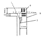
- the shortest distance between one side of the outline area 9 and a corresponding side of the display substrate is about 1.5 mm.
- the shortest distance between one side of the display substrate and a corresponding side of the upper polarizer 5 is about 0.4 mm.
- the shortest distance between one side of the outline area 9 and a corresponding side of the upper polarizer 5 is about 1.1 mm.
- the plurality of bonding pads e.g., the first bonding pads
- the shortest distance between the periphery of the outline area 9 and the periphery of the display substrate is about 1.5 mm.
- the shortest distance between the periphery of the display substrate and the periphery of the upper polarizer 5 is about 0.4 mm.
- the shortest distance between the periphery of the outline area 9 and the periphery of the upper polarizer 5 is about 1.1 mm.
- the plurality of bonding pads are disposed between the periphery of the outline area 9 and the periphery of the upper polarizer 5, for bonding the flexible display circuit board, the flexible touch control circuit board, and the flexible touch button circuit board to the connecting line 4.
- the distance between each bonding pad and a proximal side of the upper polarizer 5 and an extended line thereof is ⁇ 0.3 mm.
- the distance between each bonding pad and the first side of the upper polarizer 5 and an extended line thereof is ⁇ 0.3 mm.
- the distance between each bonding pad and the fourth side of the upper polarizer 5 and an extended line thereof is ⁇ 0.3 mm.
- the display panel further includes a plurality of second bonding pads 7 between a side (e.g., the second side) of the outline area 9 and a corresponding side (e.g., the second side) of the upper polarizer 5.
- the plurality of first bonding pads 6 and the plurality of second bonding pads 7 connect the flexible display circuit board, the flexible touch control circuit board, and the flexible touch button circuit board to the connecting line 4.
- FIGs. 3-6 are diagrams illustrating the structure of several display panels in some embodiments.
- a corner of the upper polarizer 5 in the embodiment is cut out to provide space for the plurality of side-by-side first bonding pads 6.
- the corner of the upper polarizer 5 between the first side and the fourth side is cut out, resulting in a fifth side connecting the first side and the fourth side of the upper polarizer 5.
- the angle between the first side and the fifth side of the upper polarizer 5 is in the range of about 30° to about 60°.
- the angle between the fourth side and the fifth side of the upper polarizer is in the range of about 30° to about 60°.
- the shortest distance between the first side of the outline area 9 and the first side of the upper polarizer 5 is about 1.1 mm.
- the plurality of first bonding pads 6 are a plurality of side-by-side first bonding pads 6.
- the plurality of side-by-side first bonding pads 6 extend along a direction substantially parallel to the first side of the upper polarizer 5.
- the length direction of each first bonding pad 5 is substantially parallel to the fourth side of the upper polarizer 5.
- each first bonding pad has a length of about 0.7 mm and a width about 0.1 mm.
- the plurality of bonding pads 6 may be spaced part from each other by an appropriate pitch.
- the plurality of bonding pads 6 are spaced apart from each other by a pitch of about 0.2 mm.
- the plurality of bonding pads 6 are spaced apart from each other so that they span along a direction parallel to the first side of the upper polarizer 5 by a distance in the range of about 1.5 mm to about 2.0 mm.
- the distance between each bonding pad 6 and the first side of the upper polarizer 5 and an extended line thereof is ⁇ 0.3 mm to avoid inadvertent damages (e.g., burn damage) to the upper polarizer 5.
- the plurality of first bonding pads 6 are a plurality of side-by-side first bonding pads 6.
- the plurality of side-by-side first bonding pads 6 extend along a direction substantially parallel to the first side of the upper polarizer 5.
- the length direction of each first bonding pad 5 is also substantially parallel to the first side of the upper polarizer 5.
- each first bonding pad has a length of about 0.3 mm and a width about 0.2 mm.
- the plurality of bonding pads 6 may be spaced part from each other by an appropriate pitch.
- the plurality of bonding pads 6 are spaced apart from each other by a pitch of about 0.1 mm.
- the plurality of bonding pads 6 are spaced apart from each other so that they span along a direction parallel to the first side of the upper polarizer 5 by a distance in the range of about 1.5 mm to about 2.0 mm.
- the distance between each bonding pad 6 and the first side of the upper polarizer 5 and an extended line thereof is ⁇ 0.3 mm to avoid inadvertent damages (e.g., burn damage) to the upper polarizer 5.
- the plurality of first bonding pads 6 are an array of first bonding pads 6.
- the array of first bonding pads 6 extend along a first direction substantially parallel to the first side of the upper polarizer 5, and along a second direction substantially parallel to the fourth side of the upper polarizer 5.
- the length direction of each first bonding pad 5 is substantially parallel to the first side of the upper polarizer 5, each first bonding pad has a length of about 0.3 mm and a width about 0.2 mm.
- the length direction of each first bonding pad 5 is substantially parallel to the fourth side of the upper polarizer 5, each first bonding pad has a length of about 0.3 mm and a width about 0.2 mm.
- the plurality of bonding pads 6 may be spaced part from each other by an appropriate pitch.
- the plurality of bonding pads 6 are spaced apart from each other so that they span along a direction parallel to the first side of the upper polarizer 5 by a distance in the range of about 1.5 mm to about 2.0 mm.
- the distance between each bonding pad 6 and the first side of the upper polarizer 5 and an extended line thereof is ⁇ 0.3 mm to avoid inadvertent damages (e.g., burn damage) to the upper polarizer 5.
- FIG. 6 is a diagram illustrating the structure of a portion of a display panel in some embodiments.
- the plurality of first bonding pads includes a first group of side-by-side first bonding pads 6 along a first direction and a second group of side-by-side first bonding pads 6 along a second direction perpendicular to the first direction.
- the first direction is a direction substantially parallel to the first side of the upper polarizer 5.
- the length direction of each first bonding pad 5 in the first group is substantially parallel to the fourth side of the upper polarizer 5, each first bonding pad in the first group has a length of about 0.7 mm and a width about 0.1 mm.
- each first bonding pad 5 in the second group is substantially parallel to the first side of the upper polarizer 5, each first bonding pad in the first group has a length of about 0.7 mm and a width about 0.1 mm.
- the distance between each bonding pad 6 in the first group and the first side of the upper polarizer 5 and an extended line thereof is ⁇ 0.3 mm.
- the distance between each bonding pad 6 in the second group and the fourth side of the upper polarizer 5 and an extended line thereof is ⁇ 0.3 mm.
- the plurality of bonding pads 6 may be spaced part from each other by an appropriate pitch.
- the plurality of bonding pads 6 in the first group are spaced apart from each other so that they span along a direction parallel to the first side of the upper polarizer 5 by a distance in the range of about 1.5 mm to about 2.0 mm.
- the plurality of bonding pads 6 in the second group are spaced apart from each other so that they span along a direction parallel to the fourth side of the upper polarizer 5 by a distance in the range of about 1.5 mm to about 2.0 mm.
- FIGs. 7-8 are diagrams illustrating the structure of two display panels in some embodiments. Referring to FIGs. 7-8, a corner of the upper polarizer 5 in the embodiment is not cut out. A plurality of side-by-side first bonding pads 6 is disposed between a side (e.g., the first side) of the upper polarizer 5 and a side (e.g., the first side) of the outline area 9. In FIGs. 7-8, the shortest distance between the first side of the outline area 9 and the first side of the upper polarizer 5 is about 1.1 mm.
- the plurality of first bonding pads 6 are a plurality of side-by-side first bonding pads 6.
- the plurality of side-by-side first bonding pads 6 extend along a direction substantially parallel to the first side of the upper polarizer 5.
- the length direction of each first bonding pad 5 is substantially parallel to the fourth side of the upper polarizer 5.
- each first bonding pad has a length of about 0.7 mm and a width about 0.1 mm.
- the plurality of bonding pads 6 may be spaced part from each other by an appropriate pitch.
- the plurality of bonding pads 6 are spaced apart from each other by a pitch of about 0.2 mm.
- the plurality of bonding pads 6 are spaced apart from each other so that they span along a direction parallel to the first side of the upper polarizer 5 by a distance in the range of about 1.5 mm to about 2.0 mm.
- the distance between each bonding pad 6 and the first side of the upper polarizer 5 and an extended line thereof is ⁇ 0.3 mm to avoid inadvertent damages (e.g., burn damage) to the upper polarizer 5.
- the plurality of first bonding pads 6 are a plurality of side-by-side first bonding pads 6.
- the plurality of side-by-side first bonding pads 6 extend along a direction substantially parallel to the first side of the upper polarizer 5.
- the length direction of each first bonding pad 5 is also substantially parallel to the first side of the upper polarizer 5.
- each first bonding pad has a length of about 0.3 mm and a width about 0.2 mm.
- the plurality of bonding pads 6 may be spaced part from each other by an appropriate pitch.
- the plurality of bonding pads 6 are spaced apart from each other by a pitch of about 0.1 mm.
- the plurality of bonding pads 6 are spaced apart from each other so that they span along a direction parallel to the first side of the upper polarizer 5 by a distance in the range of about 1.5 mm to about 2.0 mm.
- the distance between each bonding pad 6 and the first side of the upper polarizer 5 and an extended line thereof is ⁇ 0.3 mm to avoid inadvertent damages (e.g., burn damage) to the upper polarizer 5.
- the present disclosure provides a display apparatus having a display substrate described herein.
- appropriate display apparatuses include, but are not limited to, a liquid crystal display panel, an electronic paper, an organic light emitting display panel, a mobile phone, a tablet computer, a television, a monitor, a notebook computer, a digital album, a GPS, etc.
- the term “the invention” , “the present invention” or the like does not necessarily limit the claim scope to a specific embodiment, and the reference to exemplary embodiments of the invention does not imply a limitation on the invention, and no such limitation is to be inferred.
- the invention is limited only by the spirit and scope of the appended claims.
- these claims may refer to use “first” , “second” , etc. following with noun or element.
- Such terms should be understood as a nomenclature and should not be construed as giving the limitation on the number of the elements modified by such nomenclature unless specific number has been given. Any advantages and benefits described may not apply to all embodiments of the invention.
Abstract
Description
Claims (16)
- A display panel, comprising:a display substrate in a display area and a display circuit board electrically connected to the display substrate;a touch button in a touch button area and a touch button circuit board electrically connected to the touch button; anda connecting line for connecting the display circuit board and the touch button circuit board, the connecting line substantially outside of the display area.
- The display panel of claim 1, further comprising:a touch layer over the display substrate; anda touch control circuit board electrically connected to the touch layer, wherein the touch control circuit board is electrically connected to the touch button circuit board through the connecting line.
- The display panel of claim 2, wherein the touch layer comprises a sense electrode layer and a drive electrode layer, the connecting line is in a same layer and made of a same material as one of the sense electrode layer and the drive electrode layer.
- The display panel of claim 2, wherein the connecting line is a line circling around a peripheral area, forming a connecting line area having a first side and a second side opposite to each other, and a third side and a fourth side opposite to each other.
- The display panel of claim 2, comprising:an upper polarizer on a light emitting side of the display substrate;wherein the display panel has an outline forming an outline area, the outline area has a first side and a second side opposite to each other, and a third side and a fourth side opposite to each other; the upper polarizer has a first side and a second side opposite to each other, and a third side and a fourth side opposite to each other, each side corresponding to each side of the outline area;the display panel further comprises a plurality of first bonding pads between the first side of the outline area and the first side of the upper polarizer; wherein the plurality of first bonding pads connect the display circuit board, the touch control circuit board, and the touch button circuit board to the connecting line.
- The display panel of claim 5, wherein the upper polarizer further comprises a fifth side connecting the first side and the fourth side, the plurality of first bonding pads are at a corner between the first side and the fourth side of the outline area.
- The display panel of claim 5, wherein the upper polarizer further comprises a fifth side connecting the first side and the fourth side, the plurality of first bonding pads are about a corner between the first side and the fourth side of the outline area.
- The display panel of claim 6 or claim 7, wherein an angle between the first side and the fifth side of the upper polarizer is in the range of about 30° to about 60° .
- The display panel of any one of claims 5-7, wherein the plurality of first bonding pads are side-by-side.
- The display panel of any one of claims 5-7, wherein the plurality of first bonding pads comprises a first group of side-by-side first bonding pads along a first direction and a second group of side-by-side first bonding pads along a second direction perpendicular to the first direction.
- The display panel of any one of claims 5-7, wherein the plurality of first bonding pads comprises an array of first bonding pads.
- The display panel of any one of claims 5-11, wherein a distance between any of the plurality of the first bonding pads and the first side of the upper polarizer and an extended line thereof is≥0.3 mm.
- The display panel of any of claims 6-12, wherein a distance between any of the plurality of the first bonding pads and the fourth side of the upper polarizer and an extended line thereof is≥0.3 mm.
- The display panel of any of claims 5-13, further comprising a plurality of second bonding pads between the second side of the outline area and the second side of the upper polarizer; wherein the plurality of second bonding pads connect the connecting line to a driving chip.
- The display panel of any of claims 1-14, wherein the connecting line is completely outside of the display area.
- A display apparatus, comprising the display panel of any one of claims 1-15.
Priority Applications (1)
| Application Number | Priority Date | Filing Date | Title |
|---|---|---|---|
| US15/303,483 US10037096B2 (en) | 2015-07-10 | 2016-04-06 | Display panel and display apparatus having the same |
Applications Claiming Priority (2)
| Application Number | Priority Date | Filing Date | Title |
|---|---|---|---|
| CN201520500800.XU CN204808294U (en) | 2015-07-10 | 2015-07-10 | Display panel and display device |
| CN201520500800.X | 2015-07-10 |
Publications (1)
| Publication Number | Publication Date |
|---|---|
| WO2017008540A1 true WO2017008540A1 (en) | 2017-01-19 |
Family
ID=54593081
Family Applications (1)
| Application Number | Title | Priority Date | Filing Date |
|---|---|---|---|
| PCT/CN2016/078559 WO2017008540A1 (en) | 2015-07-10 | 2016-04-06 | Display panel and display apparatus having the same |
Country Status (3)
| Country | Link |
|---|---|
| US (1) | US10037096B2 (en) |
| CN (1) | CN204808294U (en) |
| WO (1) | WO2017008540A1 (en) |
Families Citing this family (8)
| Publication number | Priority date | Publication date | Assignee | Title |
|---|---|---|---|---|
| CN204808294U (en) * | 2015-07-10 | 2015-11-25 | 成都京东方光电科技有限公司 | Display panel and display device |
| KR102360791B1 (en) * | 2015-09-30 | 2022-02-10 | 엘지디스플레이 주식회사 | In-cell touch display device |
| KR102549718B1 (en) * | 2015-12-28 | 2023-07-03 | 삼성디스플레이 주식회사 | Touch display apparatus and method of manufacturing the same |
| CN107316883B (en) * | 2017-06-14 | 2020-06-05 | 昆山国显光电有限公司 | Manufacturing method of display panel |
| CN107256881B (en) * | 2017-06-28 | 2020-05-08 | 京东方科技集团股份有限公司 | Display panel, manufacturing method thereof and display device |
| CN109388260A (en) * | 2017-08-03 | 2019-02-26 | 北京小米移动软件有限公司 | Screen assembly and electronic equipment |
| KR102622861B1 (en) * | 2018-06-22 | 2024-01-10 | 삼성디스플레이 주식회사 | Flexible substrate and display apparatus including the same |
| CN109375820B (en) * | 2018-12-06 | 2020-06-16 | 武汉华星光电半导体显示技术有限公司 | Touch control device |
Citations (4)
| Publication number | Priority date | Publication date | Assignee | Title |
|---|---|---|---|---|
| US20110267284A1 (en) * | 2010-05-03 | 2011-11-03 | Hsin-Hao Lee | Touch-controlled electronic apparatus and related assembly method |
| US20140070875A1 (en) * | 2012-09-12 | 2014-03-13 | Synaptics Incorporated | Routing trace compensation |
| CN104375297A (en) * | 2014-12-05 | 2015-02-25 | 合肥鑫晟光电科技有限公司 | Array substrate, display panel, manufacturing method and display device |
| CN204808294U (en) * | 2015-07-10 | 2015-11-25 | 成都京东方光电科技有限公司 | Display panel and display device |
Family Cites Families (3)
| Publication number | Priority date | Publication date | Assignee | Title |
|---|---|---|---|---|
| US7619194B2 (en) * | 2007-02-26 | 2009-11-17 | Epson Imaging Devices Corporation | Electro-optical device, semiconductor device, display device, and electronic apparatus having the display device |
| KR101165456B1 (en) * | 2011-03-07 | 2012-07-12 | 이성호 | Capacitive type touch detecting means, method and touch screen panel using voltage changing phenomenon, and display device embedding said the capacitive type touch screen panel |
| KR102069808B1 (en) * | 2013-05-16 | 2020-02-12 | 삼성디스플레이 주식회사 | Organic light emitting display panel |
-
2015
- 2015-07-10 CN CN201520500800.XU patent/CN204808294U/en active Active
-
2016
- 2016-04-06 US US15/303,483 patent/US10037096B2/en active Active
- 2016-04-06 WO PCT/CN2016/078559 patent/WO2017008540A1/en active Application Filing
Patent Citations (4)
| Publication number | Priority date | Publication date | Assignee | Title |
|---|---|---|---|---|
| US20110267284A1 (en) * | 2010-05-03 | 2011-11-03 | Hsin-Hao Lee | Touch-controlled electronic apparatus and related assembly method |
| US20140070875A1 (en) * | 2012-09-12 | 2014-03-13 | Synaptics Incorporated | Routing trace compensation |
| CN104375297A (en) * | 2014-12-05 | 2015-02-25 | 合肥鑫晟光电科技有限公司 | Array substrate, display panel, manufacturing method and display device |
| CN204808294U (en) * | 2015-07-10 | 2015-11-25 | 成都京东方光电科技有限公司 | Display panel and display device |
Also Published As
| Publication number | Publication date |
|---|---|
| US20170185200A1 (en) | 2017-06-29 |
| CN204808294U (en) | 2015-11-25 |
| US10037096B2 (en) | 2018-07-31 |
Similar Documents
| Publication | Publication Date | Title |
|---|---|---|
| US10037096B2 (en) | Display panel and display apparatus having the same | |
| TWI498631B (en) | Touch sensing structure | |
| US11061266B2 (en) | Touch electrode structure and touch display device | |
| JP6104211B2 (en) | Integrated touch screen | |
| TWI477851B (en) | Touch sensing display panel and touch sensing liquid crystal display panel | |
| US8890830B2 (en) | Display device-integrated touch screen panel | |
| KR101274649B1 (en) | Liquid Crystal Display Device including Touch Panel and Method for Manufacturing the Same | |
| CN103513842B (en) | Touch panel | |
| TWI390280B (en) | Touch panel display and touch display device | |
| TWI526892B (en) | Touch panel and display device using the same | |
| US11119616B2 (en) | Trace transfer techniques for touch sensor panels with flex circuits | |
| TWI502445B (en) | Touch display device and touch substrate | |
| JP2011095806A (en) | Electrostatic capacitance-type input device, method of manufacturing electrostatic capacitance-type input device, and electro-optical device with input function | |
| US9557847B2 (en) | Touch panel, touch display panel and touch signal sensing method | |
| US20140368749A1 (en) | Method and Apparatus For Color Filter as Touch Pad | |
| US20160109981A1 (en) | In-cell touch panel and trace layout thereof | |
| US20160034076A1 (en) | Touch display device | |
| CN112732127B (en) | Display panel and display device | |
| CN112306308A (en) | Metal mesh touch electrode with visibility reduction | |
| CN111668256A (en) | Display device | |
| TWI531950B (en) | Display panel | |
| JP2012073669A (en) | Touch panel and image display device | |
| JP2011186623A (en) | Display device with touch panel | |
| TWI475444B (en) | Touch display panel and touch display device | |
| TWI573055B (en) | In-cell touch display panel |
Legal Events
| Date | Code | Title | Description |
|---|---|---|---|
| WWE | Wipo information: entry into national phase |
Ref document number: 15303483 Country of ref document: US |
|
| 121 | Ep: the epo has been informed by wipo that ep was designated in this application |
Ref document number: 16823687 Country of ref document: EP Kind code of ref document: A1 |
|
| NENP | Non-entry into the national phase |
Ref country code: DE |
|
| 122 | Ep: pct application non-entry in european phase |
Ref document number: 16823687 Country of ref document: EP Kind code of ref document: A1 |
|
| 122 | Ep: pct application non-entry in european phase |
Ref document number: 16823687 Country of ref document: EP Kind code of ref document: A1 |
|
| 32PN | Ep: public notification in the ep bulletin as address of the adressee cannot be established |
Free format text: NOTING OF LOSS OF RIGHTS PURSUANT TO RULE 112(1) EPC (EPO FORM 1205A DATED 230818) |
|
| 122 | Ep: pct application non-entry in european phase |
Ref document number: 16823687 Country of ref document: EP Kind code of ref document: A1 |