WO2017002601A1 - 電気車制御装置 - Google Patents
電気車制御装置 Download PDFInfo
- Publication number
- WO2017002601A1 WO2017002601A1 PCT/JP2016/067594 JP2016067594W WO2017002601A1 WO 2017002601 A1 WO2017002601 A1 WO 2017002601A1 JP 2016067594 W JP2016067594 W JP 2016067594W WO 2017002601 A1 WO2017002601 A1 WO 2017002601A1
- Authority
- WO
- WIPO (PCT)
- Prior art keywords
- signal
- analog
- digital
- test signal
- test
- Prior art date
- Legal status (The legal status is an assumption and is not a legal conclusion. Google has not performed a legal analysis and makes no representation as to the accuracy of the status listed.)
- Ceased
Links
Images


Classifications
-
- B—PERFORMING OPERATIONS; TRANSPORTING
- B60—VEHICLES IN GENERAL
- B60L—PROPULSION OF ELECTRICALLY-PROPELLED VEHICLES; SUPPLYING ELECTRIC POWER FOR AUXILIARY EQUIPMENT OF ELECTRICALLY-PROPELLED VEHICLES; ELECTRODYNAMIC BRAKE SYSTEMS FOR VEHICLES IN GENERAL; MAGNETIC SUSPENSION OR LEVITATION FOR VEHICLES; MONITORING OPERATING VARIABLES OF ELECTRICALLY-PROPELLED VEHICLES; ELECTRIC SAFETY DEVICES FOR ELECTRICALLY-PROPELLED VEHICLES
- B60L3/00—Electric devices on electrically-propelled vehicles for safety purposes; Monitoring operating variables, e.g. speed, deceleration or energy consumption
-
- B—PERFORMING OPERATIONS; TRANSPORTING
- B60—VEHICLES IN GENERAL
- B60L—PROPULSION OF ELECTRICALLY-PROPELLED VEHICLES; SUPPLYING ELECTRIC POWER FOR AUXILIARY EQUIPMENT OF ELECTRICALLY-PROPELLED VEHICLES; ELECTRODYNAMIC BRAKE SYSTEMS FOR VEHICLES IN GENERAL; MAGNETIC SUSPENSION OR LEVITATION FOR VEHICLES; MONITORING OPERATING VARIABLES OF ELECTRICALLY-PROPELLED VEHICLES; ELECTRIC SAFETY DEVICES FOR ELECTRICALLY-PROPELLED VEHICLES
- B60L15/00—Methods, circuits, or devices for controlling the traction-motor speed of electrically-propelled vehicles
- B60L15/40—Adaptation of control equipment on vehicle for remote actuation from a stationary place
-
- B—PERFORMING OPERATIONS; TRANSPORTING
- B61—RAILWAYS
- B61L—GUIDING RAILWAY TRAFFIC; ENSURING THE SAFETY OF RAILWAY TRAFFIC
- B61L23/00—Control, warning or like safety means along the route or between vehicles or trains
- B61L23/08—Control, warning or like safety means along the route or between vehicles or trains for controlling traffic in one direction only
- B61L23/14—Control, warning or like safety means along the route or between vehicles or trains for controlling traffic in one direction only automatically operated
-
- B—PERFORMING OPERATIONS; TRANSPORTING
- B61—RAILWAYS
- B61L—GUIDING RAILWAY TRAFFIC; ENSURING THE SAFETY OF RAILWAY TRAFFIC
- B61L3/00—Devices along the route for controlling devices on the vehicle or train, e.g. to release brake or to operate a warning signal
- B61L3/02—Devices along the route for controlling devices on the vehicle or train, e.g. to release brake or to operate a warning signal at selected places along the route, e.g. intermittent control simultaneous mechanical and electrical control
- B61L3/08—Devices along the route for controlling devices on the vehicle or train, e.g. to release brake or to operate a warning signal at selected places along the route, e.g. intermittent control simultaneous mechanical and electrical control controlling electrically
- B61L3/12—Devices along the route for controlling devices on the vehicle or train, e.g. to release brake or to operate a warning signal at selected places along the route, e.g. intermittent control simultaneous mechanical and electrical control controlling electrically using magnetic or electrostatic induction; using radio waves
Definitions
- Embodiments of the present invention relate to an electric vehicle control device.
- an automatic train stop device (Automatic Train Stop)
- ATC Automatic Train Control
- security devices As driving assistance devices, automatic driving devices (ATO (Automatic Train Operation)) and fixed position stop devices (TASC (Train Automatic Stop-position Controller) are known.
- ATO Automatic Train Operation
- TASC Train Automatic Stop-position Controller
- These electric vehicle control devices in these safety devices and driving support devices collectively convert analog signals received from the ground into digital signals, and control the electric vehicles based on the digital signals.
- the receiving unit of such an electric vehicle control device may be configured in a parallel dual system so as to ensure its own soundness and to detect a failure when a failure occurs.
- the analog signal processing unit is composed of analog elements in the receiving unit, there are variations in characteristics. Therefore, if the analog signal processing unit is a parallel dual system, variations occur between the signals processed by the two analog signal processing units. Since the characteristic variation of the analog element is not a failure, it is necessary to set the determination standard for determining the soundness of the signal processing system so as to allow the characteristic variation of the analog signal processing unit. This makes it difficult to accurately determine the soundness of the signal processing system, and it becomes difficult to accurately detect a failure of the on-vehicle receiving unit.
- a standby dual system may be adopted so that the electric vehicle does not become inoperable.
- both the standby duplex system and the parallel duplex system are applied to the on-vehicle receiver, a total of four signal processing systems are required. In this case, the size of the on-vehicle receiving unit is increased, and the installation area is increased.
- ⁇ Provide a small electric vehicle control device that can accurately detect abnormalities in the signal processing system.
- the electric vehicle control apparatus includes an analog signal processing unit that processes an analog reception signal received via an antenna.
- the analog / digital conversion unit converts the analog signal from the analog signal processing unit into a digital signal.
- the digital signal processing unit processes a digital signal.
- the control unit controls the electric vehicle based on the digital signal from the digital signal processing unit.
- the test signal generation unit provides the analog signal processing unit with an analog test signal different from the analog reception signal in frequency or signal content.
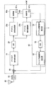
- FIG. 1 is a block diagram illustrating an example of a configuration of an electric vehicle control device 1 (hereinafter also referred to as a control device 1) according to the present embodiment.
- the control device 1 is mounted on an electric vehicle such as a railroad, and receives a signal from a ground element with an antenna (for example, a vehicle upper element, a power receiver) 95 and sends the signal to the control device 1 via a transformer 90. input.
- the control device 1 processes a signal from the ground unit and outputs a control signal CNT.
- the control signal CNT is used for controlling the electric vehicle.
- the control device 1 includes an analog signal processing unit 10, an ADC (Analog-to-Digital Converter) 20, digital signal processing units 30a and 30b, control units 40a and 40b, a test signal generation unit 50, and an addition unit 80. I have.
- the control device 1 may be configured as a standby dual system.
- the standby duplex system has a configuration in which a plurality of signal processing systems are provided, and when one signal processing system fails, the signal processing is switched to the other signal processing system. Therefore, when the control device 1 is configured as a standby dual system, two signal processing systems from the analog signal processing unit 10 to the control units 40a and 40b are connected in parallel.
- the analog signal processing unit 10 performs analog processing (for example, amplification processing and filtering processing) so that the analog reception signal received by the antenna 95 and the analog test signal from the test signal generation unit 50 can be digitally converted by the ADC 20.
- analog processing for example, amplification processing and filtering processing
- the ADC 20 as an analog / digital conversion unit converts the analog reception signal and the analog test signal processed by the analog signal processing unit 10 into a digital signal.
- Both the digital signal processing units 30a and 30b receive the digital signal from the ADC 20 and digitally process the digital signal.
- the digital signal processing units 30a and 30b convert the digital signal into the frequency domain by performing a Fourier transform.
- the digital signal processing units 30a and 30b take out a signal level (signal strength) at a certain frequency from the digital signal and output the frequency and signal level to the control units 40a and 40b.
- the digital signal processing units 30a and 30b transmit the resonance frequency and the signal level at the resonance frequency when the ground unit and the antenna 95 are electromagnetically coupled to the control units 40a and 40b as digital control signals.
- the digital signal processing units 30a and 30b transmit a predetermined frequency and a signal level at the frequency to the control units 40a and 40b as digital test signals.
- the digital control signal is used to generate a control signal CNT for controlling the electric vehicle.
- the digital test signal is used to confirm the soundness of the analog signal processing unit 10 and the ADC 20. Soundness means that the device is not malfunctioning and is operating normally.
- the digital control signal and the digital test signal are collectively referred to as a digital signal.
- the control units 40a and 40b generate the control signal CNT based on the frequency and signal level received from the digital signal processing units 30a and 30b, or check the soundness of the control device 1.
- the storage units 41a and 41b store in advance a reference pattern of normal digital test signals.
- the reference pattern of the normal digital test signal is used when confirming the soundness of the analog signal processing unit 10 and the ADC 20 and has a predetermined frequency and a predetermined signal level.
- a plurality of digital signal processing units 30a and 30b and control units 40a and 40b that execute digital signal processing are provided, and constitute a parallel dual system.
- the parallel duplex system connects two identical signal processing systems in parallel and compares (matches) signals processed by both signal processing systems. If both signals are equal as a result of the comparison, the two signal processing systems can be confirmed to be healthy.
- the first system and the second system have the same configuration. That is, the digital signal processing units 30a and 30b have the same configuration, and the control units 40a and 40b also have the same configuration.
- the first system and the second system receive the same digital signal. Therefore, when both the first system and the second system are normal, the first system and the second system should process the digital signal in the same manner and output the same control signal CNT. Therefore, the control unit 40a or 40b compares (matches) the frequency and signal level of the digital signal in the control unit 40a with the frequency and signal level of the digital signal in the control unit 40b.
- control part 40a, 40b can confirm the soundness of the structure after digital signal processing part 30a, 30b.
- the digital signal processing units 30a and 30b and the control units 40a and 40b that execute digital signal processing are collectively referred to as a digital signal processing system.
- analog signal processing unit 10 and the ADC 20 that execute analog signal processing are not a parallel dual system but are configured by one system. This is because the digital signals input to the digital signal processing units 30a and 30b are the same.
- analog signal processing unit 10 and the ADC 20 are also configured in a parallel dual system, as described above, variations between the two analog reception signals occur due to variations in characteristics of the analog elements.
- the timing of changing the digital control signal output from the ADC 20 varies.
- the digital signals input to the digital signal processing units 30a and 30b cannot be made the same, and it is difficult to accurately check the soundness of the digital signal processing system.
- the analog signal processing unit 10 and the ADC 20 are configured in one system, so that the digital signals input to the digital signal processing units 30a and 30b are the same signal (common signal). be able to. Thereby, control part 40a, 40b can confirm the soundness of the said digital signal processing system correctly.
- the analog signal processing unit 10 and the ADC 20 that execute analog signal processing are collectively referred to as an analog signal processing system.
- the test signal generator 50 outputs an analog test signal to the adder 80 in response to a command from the controller 40a or 40b.
- the analog test signal is a signal used for detecting a failure of the analog signal processing system, and is processed by the analog signal processing system and the digital signal processing system together with the analog reception signal.
- the test signal generator 50 includes a digital test signal generator 51, a DAC (Digital-to-Analog Converter) 52, and an analog test signal output unit 53.
- the digital test signal generator 51 receives a command from the controller 40a or 40b and generates a digital test signal.
- the digital test signal is a signal indicating a predetermined level (signal strength) as a digital value at a predetermined frequency.
- the DAC 52 converts the digital test signal into analog and outputs the analog test signal.
- the analog test signal output unit 53 receives the analog test signal from the DAC 52, amplifies the analog test signal, and outputs it to the adder 80.
- the analog test signal becomes a signal having a predetermined level (signal strength) at a predetermined frequency based on the digital test signal.
- the frequencies and signal levels of the digital test signal and the analog test signal are preset and stored in the control units 40a and 40b.
- the adder 80 is provided between the transformer 90 and the input unit of the analog signal processing unit 10, and between the output of the test signal generation unit 50 and the input unit of the analog signal processing unit 10.
- the adder 80 adds the analog test signal from the test signal generation unit 50 to the analog reception signal from the antenna 95 and outputs it to the analog signal processing unit 10.
- the analog reception signal and the analog test signal are collectively referred to as an analog signal.
- the analog signal is processed by an analog signal processing system and converted into a digital signal.
- the analog test signal is simultaneously processed without being distinguished from the analog reception signal, and is converted into a digital signal by the ADC 20.
- the digital signal is output to the digital signal processing units 30a and 30b.
- the digital signal processing units 30a and 30b convert the digital signal into a frequency domain by Fourier transform, and extract a digital control signal and a digital test signal from the digital signal.
- the control units 40a and 40b output the control signal CNT based on the digital control signal, and confirm the soundness of the analog signal processing system based on the digital test signal.
- a digital test signal during normal operation is referred to as a normal digital test signal.
- the storage units 41a and 41b store a reference pattern of normal digital test signals in advance, and compare them with the digital test signals from the digital signal processing units 30a and 30b, respectively.
- the reference pattern of the normal digital test signal may be set using a digital test signal obtained by actually inputting the analog test signal to the analog signal processing unit 10, ADC 20, or the like during normal operation.
- the reference pattern of the normal digital test signal may be set in common to the plurality of control devices 1 using a statistically obtained average normal digital test signal.
- the control units 40a and 40b It is determined that the signal processing unit 10 and the ADC 20 are operating normally.
- the control device 1 can check the soundness of the analog signal processing system using the test signal without making the analog signal processing system a parallel dual system.
- the digital test signal is used for confirming the soundness of the analog signal processing system. That is, as long as the soundness of the digital signal processing system is ensured by the parallel duplex system, the digital test signal may be used to check the soundness of the analog signal processing system.
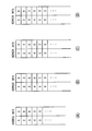
- FIGS. 2 (A) to 2 (D) are conceptual diagrams showing an example of the comparison and collation operation in the control units 40a and 40b.
- FIG. 2A shows a reference pattern of a normal digital test signal stored in the register.
- the reference pattern of the normal digital test signal is stored in advance in the storage units 41a and 41b.
- the control units 40a and 40b generate a predetermined analog test signal from the test signal generation unit 50 based on the reference pattern of the normal digital test signal.
- ADDRESS indicates the address of the write register
- DATA indicates the level of the analog test signal.
- DATA indicates the level of the analog test signal. For example, when DATA is 1, the level of the analog test signal is ⁇ 40 dBv. When DATA is 2, the level of the analog test signal is ⁇ 35 dBv. When DATA is 3, the level of the analog test signal is ⁇ 30 dBv. Thus, every time the DATA value increases by 1, the level of the analog test signal increases by 5 dBv. That is, each time the DATA value changes, the level of the analog test signal changes.
- DATA of each ADDRESS is read in the order of ADDESS.
- the read time interval is set to a predetermined time interval (for example, 50 ms). Therefore, for example, when DATA shown in each ADDRESS is read and executed at an interval of 50 ms, the level of the analog test signal is 3 (for example, ⁇ 30 dBv), 0 (for example, ⁇ 45 dBv), 0 for every 50 ms. (For example, ⁇ 45 dBv), 3 (for example, ⁇ 30 dBv), and 0 (for example, ⁇ 45 dBv).
- the control units 40a and 40b can generate the analog test signal from the test signal generation unit 50 based on the reference pattern of the normal digital test signal.
- ADDRESS and DATA are not limited and are arbitrary.
- control units 40a and 40b respectively compare the ADDRESS 1 to 5 DATA of the reference pattern in FIG. 2A and the ADDRESS 2 to 6 DATA of the result pattern in FIG. 2B. To do.
- the result pattern in FIG. 2B is within the allowable range with respect to the reference pattern in FIG. , 40b determine that the analog signal processing system is normal.
- control units 40a and 40b determine that the analog signal processing system is abnormal.
- the result pattern in FIG. 2D is out of the allowable range with respect to the reference pattern in FIG. Also in this case, the control units 40a and 40b determine that the analog signal processing system is abnormal.
- control units 40a and 40b When it is determined that the analog signal processing system is abnormal, the control units 40a and 40b display a warning on the monitor for the crew of the electric vehicle or issue a warning. Or control part 40a, 40b may control the brake of an electric vehicle, or may transmit that to the exterior (ground child etc.) of an electric vehicle.
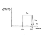
- FIG. 3 is a graph showing an example of the relationship between the frequency band Scnt of the analog reception signal and the frequency band Test of the analog test signal.
- the vertical axis indicates the signal level (signal strength or gain).
- the horizontal axis indicates the frequency.
- the digital control signal and the digital test signal are different in form from the analog reception signal and the analog test signal, they have the same characteristics (frequency and signal level) as the analog reception signal and the analog test signal, respectively. Therefore, illustration of the frequency bands of the digital reception signal and the digital test signal is omitted.
- the frequency band Scnt that the analog reception signal can take is defined by standards and the like.
- the frequency band Stest of the analog test signal is set to the high band side or the low band side of the frequency band Scnt of the analog reception signal
- the peak frequency Fp of the analog test signal is the frequency band Scnt of the analog reception signal.
- the peak frequency Fp of the analog test signal is in the vicinity of the maximum value Fmax of the frequency band Scnt of the analog reception signal and is larger than the maximum value Fmax (Fp> Fmax). Since the peak frequency Fp is larger than the maximum value Fmax, the control units 40a and 40b can distinguish between the digital control signal and the digital test signal by the difference in frequency after the digital signal processing.
- the peak frequency Fp exceeds the maximum value Fmax, but is in the vicinity of the maximum value Fmax.
- control part 40a, 40b can test an analog signal processing system using the analog test signal which has a frequency close
- the peak frequency Fp of the analog test signal is set to the lower side of the frequency band Scnt of the analog reception signal
- the peak frequency Fp of the analog test signal is equal to the frequency band Scnt of the analog reception signal.
- the control units 40a and 40b can distinguish between the digital control signal and the digital test signal according to the frequency difference after the digital signal processing.
- control part 40a, 40b can test an analog signal processing system using the analog test signal which has a frequency close
- the strength of the analog test signal within the frequency band Scnt of the analog reception signal is set to be equal to or less than the noise level (thermal noise level) NL of the analog reception signal.
- the intensity of the analog test signal is equal to or lower than the noise level NL of the analog reception signal at a frequency equal to or lower than the maximum value Fmax.
- the peak frequency Fp of the analog test signal is in the vicinity and outside of the frequency band Scnt of the analog reception signal. Further, the strength of the analog test signal in the frequency band Scnt of the analog reception signal is equal to or lower than the noise level NL of the analog reception signal.
- control part 40a, 40b can confirm the soundness of an analog signal processing system correctly using the frequency close
- FIG. 4 is a graph showing an analog test signal pattern.
- the vertical axis of this graph indicates the signal level (signal strength or gain) of the analog test signal.
- the horizontal axis indicates time.
- the analog test signal in this graph is obtained by extracting the analog test signal from the signal input to the ADC 20 through the analog signal processing unit 10. Therefore, the analog test signal added in the adder 80 may contain noise N.
- the analog test signal pattern is generated by the test signal generator 50 in response to an instruction from the controller 40b or 40a.
- the analog test signal is periodically output in a pattern of a predetermined signal level.
- t1, t2 to t3 and t4 to t5 are periods in which the signal level of the analog test signal is zero (that is, the analog test signal is not output). Therefore, when the analog signal processing unit 10 is normal and there is no noise N, the signal levels before t1, t2 to t3, and t4 to t5 are below the threshold value Sth.
- the threshold value Sth indicates the lowest signal level detected by the control units 40a and 40b as a signal. Further, the signal level that the analog reception signal can take is defined by a standard or the like. Therefore, the threshold value Sth may be said to be the lower limit of the standard of the signal level that the analog reception signal can take.
- the analog test signal has a signal level (first signal strength) close to the lower limit although it is larger than the lower limit (threshold value Sth) of the standard of the signal level.
- the signal level of the analog test signal becomes zero.
- the analog test signal has a signal level (second signal strength) close to the upper limit although it is smaller than the upper limit of the standard of the signal level.
- the signal level of the analog test signal becomes zero.
- the analog test signal periodically repeats the signal having the first signal strength near the lower limit and the signal having the second signal strength near the upper limit within the range of the signal level standard.
- the control part 40a or 40b can confirm the soundness of an analog signal processing system in the whole range of the standard of a received signal level. That is, the soundness of the dynamic range over a wide range of the analog signal processing system can be confirmed.
- noise N is generated from t2 to t3. Since the noise N is different from the failure of the analog signal processing system, the control units 40a and 40b need to make a determination by removing the noise N. For example, noise usually occurs only for a short time in a transient manner, and failure of an analog signal processing system continuously generates an abnormal signal. Therefore, the control units 40a and 40b may determine the noise based on the noise generation period (period in which the noise level exceeds the threshold value Sth). For example, a noise allowable period (for example, about 10 ms) is set in advance, and the control units 40a and 40b determine that the abnormal signal is noise when the abnormal signal generation period is equal to or shorter than the noise allowable period.
- a noise allowable period for example, about 10 ms
- the control units 40a and 40b do not use the abnormal signal determined to be noise to determine the soundness of the analog signal processing system. Thereby, even if noise is included in the analog test signal, the control units 40a and 40b can accurately determine the soundness of the analog signal processing system.
- FIG. 5 is a graph showing another example of an analog test signal pattern.
- the analog test signal shown in FIG. 5 has any (intermediate) signal strength (hereinafter also referred to as standard signal strength) between the lower limit and the upper limit of the standard of the analog reception signal.
- the analog test signal periodically repeats the standard signal strength. For example, from time t11 to t12, the analog test signal has a standard signal strength. Next, from t12 to t13, the signal level of the analog test signal becomes zero. Thereafter, the analog test signal repeats the signal pattern from t11 to t13. In this way, the analog test signal may periodically repeat the standard signal strength that is between the upper limit and the lower limit of the standard range of the received signal level. Even with such an analog test signal pattern, the soundness of the analog signal processing system can be confirmed.
- the noise N1 is generated before t11, and the noise N2 is generated from t11 to t12.
- the determination of the noises N1 and N2 may be the same as the determination of the noise N described with reference to FIG. Therefore, when the noise N1 and N2 generation period (period in which the noise signal intensity exceeds the threshold Sth) is equal to or less than the noise allowable period, the control units 40a and 40b treat the noise N1 and N2 as soundness of the analog signal processing system. Not used for judgment. Thereby, even if the noises N1 and N2 are included in the analog test signal, the control units 40a and 40b can accurately determine the soundness of the analog signal processing system.
- FIG. 6 is a graph showing the relationship between the frequency band Scnt of the analog reception signal and the frequency band Test of the analog test signal according to the modification.
- the vertical axis indicates the signal level (signal strength or gain).
- the horizontal axis indicates the frequency.
- the digital control signal and the digital test signal are different in form from the analog reception signal and the analog test signal, they exhibit the same characteristics (frequency and signal level) as the analog reception signal and the analog test signal, respectively.
- the analog test signal is transmitted using two frequency bands.
- the frequency band Test_H of the analog test signal is set on the high frequency side of the frequency band Scnt of the analog reception signal, and the peak frequency (first frequency) Fp_H of the analog test signal is , Near and outside the frequency band Scnt of the analog received signal.
- the peak frequency Fp_H of the analog test signal is in the vicinity of the maximum value Fmax of the frequency band Scnt of the analog reception signal and is larger than the maximum value Fmax (Fp_H> Fmax).
- control units 40a and 40b can distinguish between the digital control signal and the digital test signal by the difference in frequency after the digital signal processing.
- the peak frequency Fp_H exceeds the maximum value Fmax, but is in the vicinity of the maximum value Fmax. Thereby, control part 40a, 40b can test an analog signal processing system using the frequency close
- the frequency band Stest_L of the analog test signal is set on the lower side of the frequency band Scnt of the analog reception signal, and the peak frequency Fp_L of the analog test signal is near and outside the frequency band Scnt of the analog reception signal.
- the peak frequency (second frequency) Fp_L of the analog test signal is in the vicinity of the minimum value Fmin of the frequency band Scnt of the analog reception signal and is smaller than the minimum value Fmin (Fp_L ⁇ Fmin).
- the control units 40a and 40b can distinguish between the digital control signal and the digital test signal by the difference in frequency after the digital signal processing.
- control part 40a, 40b can test an analog signal processing system using the frequency close
- the strength of the analog test signal within the frequency band Scnt of the analog reception signal is set to be equal to or less than the noise level (thermal noise level) NL of the analog reception signal.
- the strength of the analog test signal in the frequency band from the minimum value Fmin to the maximum value Fmax is equal to or lower than the noise level NL of the analog reception signal.
- the frequency of the analog test signal is set to two frequency bands Stest_L and Test_H on both sides of the frequency band Scnt of the analog reception signal.
- the control units 40a and 40b can perform the analog operation in the entire frequency band Scnt between the frequency band Test_L and the frequency band Stest_H. It can be assumed that the signal processing system is healthy.
- FIG. 7 is a graph showing an analog test signal pattern according to a modification.
- the analog test signal periodically repeats a certain signal strength (for example, standard signal strength) in each of the frequency band (first frequency) Test_H and the frequency band (second frequency) Test_L.
- the analog test signal rises alternately at different timings in the frequency band Test_L and the frequency band Test_H.
- the analog test signal in the frequency band Test_L has the standard signal strength at times t23 to t24 and t27 to t28, and the period of the standard signal strength is t23 to t27.
- the analog test signal in the frequency band Test_H has a standard signal intensity at times t21 to t22 and t25 to t26, and a period of the standard signal intensity is t21 to t25. That is, the generation period of the analog test signal in the frequency band Test_L and the generation period of the analog test signal in the frequency band Test_H are shifted from each other by a half period. Thereby, it can suppress that the amplifier of ADC20 is saturated.
- control units 40a and 40b can confirm the soundness of the analog signal processing system in both the frequency band Test_H and the frequency band Test_L. Since the analog test signal in the frequency band Test_L and the analog test signal in the frequency band Test_H are shifted from each other by a half cycle, the control units 40a and 40b may frequently detect failures in the analog signal processing system in a relatively short cycle. it can. That is, the duty ratio for failure detection can be increased. Furthermore, in this modification, the failure detection cycle of the analog signal processing system by the control units 40a and 40b can be made shorter than the failure detection cycle defined in the specifications of the safety device or the driving support device. As a result, the control units 40a and 40b detect a failure of the analog signal processing system within the failure detection cycle defined in the specification, and display a warning on the monitor (not shown) of the electric vehicle accordingly. Alternatively, the brake can be controlled.
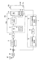
- FIG. 8 is a block diagram showing an example of the configuration of the electric vehicle control device 2 according to the second embodiment.
- the second embodiment is different from the first embodiment in that the digital signal processing unit 30 a includes a bit monitor 32. Other configurations of the second embodiment may be the same as the corresponding configurations of the first embodiment.
- the digital signal processing unit 30a is configured by, for example, a one-chip FPGA (Field Programmable Gate Array), and includes an input unit 31, a filter processing unit 33, and an output unit 34.
- the control unit 40a is communicably connected to the output unit 34 via the VME bus.
- the control unit 40a may be configured with a one-chip CPU, for example.
- the digital signal processing unit 30a and the control unit 40a are illustrated, and the digital signal processing unit 30b and the control unit 40b are not illustrated.
- the digital signal processing unit 30b may be configured by a one-chip FPGA, similarly to the digital signal processing unit 30a.
- the control unit 40b may be composed of a one-chip CPU, like the control unit 40a.
- the bit monitor 32 is provided in the input unit 31 and monitors the bits of the digital test signal from the ADC 20.
- the test signal generator 50 periodically and repeatedly outputs an analog test signal while the electric vehicle is running and stopped. Accordingly, the bit monitor 32 monitors the bit change of the digital control signal at a period longer than or equal to the input period of the analog test signal.
- the bits of the digital control signal should change with the periodic change of the analog test signal. However, if the bits of the digital control signal do not change over a predetermined period (the period of the analog test signal) and are fixed, there is a high possibility that the analog signal processing system has failed. In this case, the digital signal processing units 30a and 30b output error signals to the control units 40a and 40b. The control units 40a and 40b may determine that the analog signal processing system is abnormal when receiving an error signal.
- the bit monitor 32 may monitor the bit of the digital control signal instead of the digital test signal or together with the digital test signal while the electric vehicle is running. This is because the bit of the digital control signal can be fixed while the electric vehicle is stopped, but fluctuates frequently while the electric vehicle is running. Therefore, the bit monitor 32 may determine the abnormality of the analog signal processing system by monitoring the bit of the digital control signal while the electric vehicle is traveling.
- the bit monitor 32 monitors the bit of the digital test signal or the digital control signal, and the control units 40a and 40b detect the abnormality of the analog signal processing system based on the fixed time of the bit of the digital test signal or the digital control signal. May be judged. Thereby, 2nd Embodiment can confirm the soundness of ADC20 easily.
- the second embodiment can also obtain the effects of the first embodiment.
- FIG. 9 is a conceptual diagram showing an example of the operation of the electric vehicle control device according to the third embodiment.
- the frequency bandwidth of the control signal may be limited by a band pass filter. In this case, it is difficult to set the frequency of the analog test signal outside the frequency band of the analog reception signal.
- the frequency of the analog test signal is set within the frequency band of the analog reception signal, and the signal content (telegram) is distinguished.
- the telegram of the analog test signal is a telegram that cannot be used (not meaningful) in the analog reception signal, and is always different from the telegram of the analog reception signal. More specifically, an enumeration of the same characters can be considered as a telegram of an analog test signal.
- the configuration of the control device of the third embodiment may be the same as the configuration of any of the control devices of the first or second embodiment.
- the test signal generation unit 50 intermittently outputs the analog test signal at a constant period.
- the control units 40a and 40b can confirm the soundness of the analog signal processing system based on the digital test signal corresponding to the analog test signal.
- the control units 40a and 40b adopt a message when two of the four consecutive messages can be accurately demodulated. This is referred to as the 4 C 2 test.
- the test signal generating unit 50 immediately stops the generation of the analog test signal.
- the control units 40a and 40b can accurately demodulate at least two of the four consecutive messages. If the analog test signal overlaps with the first telegram of the analog reception signal, the first telegram may not be demodulated, but the subsequent second to fourth telegrams can be demodulated. If the analog test signal does not overlap the first telegram of the analog reception signal, the test signal generator 50 immediately stops generating the analog test signal after receiving the first telegram. In this case, all the first to fourth messages can be demodulated.
- the control units 40a and 40b can demodulate and identify both the analog reception signal and the analog test signal. Thereby, the soundness of an analog signal processing system can be confirmed.
Landscapes
- Engineering & Computer Science (AREA)
- Mechanical Engineering (AREA)
- Power Engineering (AREA)
- Transportation (AREA)
- Life Sciences & Earth Sciences (AREA)
- Sustainable Development (AREA)
- Sustainable Energy (AREA)
- Electric Propulsion And Braking For Vehicles (AREA)
- Train Traffic Observation, Control, And Security (AREA)
Abstract
本実施形態による電気車制御装置は、アンテナを介して受信したアナログ受信信号を処理するアナログ信号処理部を備える。アナログ・デジタル変換部は、アナログ信号処理部からのアナログ信号をデジタル信号へ変換する。デジタル信号処理部は、デジタル信号を処理する。制御部は、デジタル信号処理部からのデジタル信号に基づいて電気車を制御する。試験信号発生部は、周波数または信号内容においてアナログ受信信号と異なるアナログ試験信号をアナログ信号処理部に与える。
Description
本発明の実施形態は、電気車制御装置に関する。
鉄道に用いられる電気車が安全に走行しかつ停止するために、様々な保安装置や運転支援装置が開発されている。例えば、保安装置として、自動列車停止装置(ATS(Automatic Train Stop))および自動列車制御装置(ATC(Automatic Train Control))が知られている。また、運転支援装置として、自動運転装置(ATO(Automatic Train Operation))、定位置停止装置(TASC(Train Automatic Stop-position Controller))が知られている。
これらの保安装置および運転支援装置における電気車制御装置は、地上から受けたアナログ信号を一括でデジタル信号へ変換し、そのデジタル信号に基づいて電気車の制御を行う。このような電気車制御装置の受信部は、自己の健全性を確保し、故障した場合には故障を検知できるように、並列2重系で構成される場合がある。
しかし、受信部内において、アナログ信号処理部は、アナログ素子で構成されているため特性にばらつきが存在する。従って、アナログ信号処理部を並列2重系にすると、2つのアナログ信号処理部で処理された信号間にばらつきが生じてしまう。このようなアナログ素子の特性ばらつきは故障ではないので、信号処理システムの健全性を判定するための判定基準は、アナログ信号処理部の特性ばらつきを許容するように設定する必要が生じる。これでは、信号処理システムの健全性を正確に判定することが困難になり、車上受信部の故障を正確に検知することが困難になってしまう。
また、信号処理システムが故障した場合であっても、電気車が走行不能にならないように、待機2重系が採用される場合がある。しかし、待機2重系および並列2重系の両方を車上受信部に適用すると、合計4つの信号処理システムが必要となる。この場合、車上受信部のサイズが大きくなり、その設置面積が大きくなってしまう。
信号処理システムの異常を正確に検知することができ、かつ、サイズの小さな電気車制御装置を提供する。
本実施形態による電気車制御装置は、アンテナを介して受信したアナログ受信信号を処理するアナログ信号処理部を備える。アナログ・デジタル変換部は、アナログ信号処理部からのアナログ信号をデジタル信号へ変換する。デジタル信号処理部は、デジタル信号を処理する。制御部は、デジタル信号処理部からのデジタル信号に基づいて電気車を制御する。試験信号発生部は、周波数または信号内容においてアナログ受信信号と異なるアナログ試験信号をアナログ信号処理部に与える。
以下、図面を参照して本発明に係る実施形態を説明する。本実施形態は、本発明を限定するものではない。
図1は、本実施形態による電気車制御装置1(以下、制御装置1ともいう)の構成の一例を示すブロック図である。制御装置1は、鉄道等の電気車に搭載されており、地上子からの信号をアンテナ(例えば、車上子、受電器)95で受信し、トランス90を介して該信号を制御装置1に入力する。制御装置1は、地上子からの信号を処理して制御信号CNTを出力する。制御信号CNTは、電気車を制御するために用いられる。
制御装置1は、アナログ信号処理部10と、ADC(Analog to Digital Convertor)20と、デジタル信号処理部30a、30bと、制御部40a、40bと、試験信号発生部50と、加算部80とを備えている。尚、図示していないが、制御装置1は、待機2重系として構成されていてもよい。待機2重系は、複数の信号処理システムを設け、一方の信号処理システムが故障した場合に、他方の信号処理システムに切り換えて信号処理を行う構成である。従って、制御装置1が待機2重系として構成される場合、アナログ信号処理部10から制御部40a、40bまでの信号処理システムが2つ並列に接続される。
アナログ信号処理部10は、アンテナ95で受信したアナログ受信信号および試験信号発生部50からのアナログ試験信号をADC20においてデジタル変換できるようにアナログ処理(例えば、増幅処理、フィルタリング処理)する。
アナログ・デジタル変換部としてのADC20は、アナログ信号処理部10で処理されたアナログ受信信号およびアナログ試験信号をデジタル信号へ変換する。
デジタル信号処理部30a、30bは、ともにADC20からのデジタル信号を受け取り、該デジタル信号をデジタル処理する。例えば、デジタル信号処理部30a、30bは、デジタル信号をフーリエ変換することによって周波数領域に変換する。さらに、デジタル信号処理部30a、30bは、デジタル信号から或る周波数における信号レベル(信号強度)を取り出して、その周波数や信号レベルを制御部40a、40bへ出力する。例えば、デジタル信号処理部30a、30bは、地上子とアンテナ95との電磁結合したときの共振周波数および共振周波数における信号レベルをデジタル制御信号として制御部40a、40bへ送信する。あるいは、デジタル信号処理部30a、30bは、所定の周波数およびその周波数における信号レベルをデジタル試験信号として制御部40a、40bへ送信する。デジタル制御信号は、電気車を制御するための制御信号CNTを生成するために用いられる。デジタル試験信号は、アナログ信号処理部10やADC20の健全性を確認するために用いられる。健全性は、装置が故障しておらず正常に動作していることを意味する。尚、デジタル制御信号およびデジタル試験信号を、まとめて、デジタル信号とも呼ぶ。
制御部40a、40bは、デジタル信号処理部30a、30bから受け取った周波数や信号レベルに基づいて制御信号CNTを生成し、あるいは、制御装置1の健全性を確認する。記憶部41a、41bは、正常デジタル試験信号の参照パターンを予め格納している。正常デジタル試験信号の参照パターンは、アナログ信号処理部10、ADC20の健全性を確認する際に用いられ、所定の周波数および所定の信号レベルを有する。
ここで、本実施形態において、デジタル信号処理を実行するデジタル信号処理部30a、30bおよび制御部40a、40bは、それぞれ複数設けられており、並列2重系を構成している。並列2重系は、2つの同じ信号処理システムを並列に接続し、両方の信号処理システムで処理した信号を比較照合する(突き合わせる)。比較照合の結果、両方の信号が等しい場合、該2つの信号処理システムは健全であると確認することができる。
デジタル信号処理部30aおよび制御部40aを第1系とし、デジタル信号処理部30bおよび制御部40bを第2系とすると、第1系と第2系とは同一の構成を有する。即ち、デジタル信号処理部30a、30bは、互いに同一の構成であり、制御部40a、40bも、互いに同一の構成である。また、第1系および第2系は、同一のデジタル信号を受け取る。従って、第1系および第2系がともに正常である場合、第1系および第2系は、デジタル信号を同様に処理し、同一の制御信号CNTを出力するはずである。そこで、制御部40aまたは40bは、制御部40aにおけるデジタル信号の周波数や信号レベルと制御部40bにおけるデジタル信号の周波数や信号レベルとを比較照合する(付き合わせる)。これにより、制御部40a、40bにおけるデジタル信号の周波数や信号レベルがほぼ同一である場合には、第1系および第2系がともに正常であることが分かる。制御部40a、40bにおけるデジタル信号の周波数や信号レベルが大きく異なる場合には、第1系または第2系が異常を有していることが分かる。これにより、制御部40a、40bは、デジタル信号処理部30a、30b以降の構成の健全性を確認することができる。以下、デジタル信号処理を実行するデジタル信号処理部30a、30bおよび制御部40a、40bを、まとめてデジタル信号処理システムともいう。
一方、アナログ信号処理を実行するアナログ信号処理部10およびADC20は、並列2重系にはなっておらず、1つの系で構成されている。これは、デジタル信号処理部30a、30bに入力されるデジタル信号を同一にするためである。
もし、アナログ信号処理部10およびADC20も並列2重系で構成されている場合、上述の通り、アナログ素子の特性ばらつきによって、2つのアナログ受信信号間にばらつきが生じてしまう。アナログ受信信号がばらつくと、ADC20から出力されるデジタル制御信号の変化のタイミング等がばらつく。この場合、デジタル信号処理部30a、30bに入力されるデジタル信号を同一にすることができず、上記デジタル信号処理システムの健全性を正確に確認することが困難になってしまう。
これに対し、本実施形態では、アナログ信号処理部10およびADC20は、1つの系で構成されているので、デジタル信号処理部30a、30bに入力されるデジタル信号を同一信号(共通信号)にすることができる。これにより、制御部40a、40bは、上記デジタル信号処理システムの健全性を正確に確認することができる。以下、アナログ信号処理を実行するアナログ信号処理部10およびADC20を、まとめてアナログ信号処理システムともいう。
試験信号発生部50は、制御部40aまたは40bからの命令を受けて、アナログ試験信号を加算器80へ出力する。アナログ試験信号は、アナログ信号処理システムの故障を検知するために用いられる信号であり、アナログ受信信号とともにアナログ信号処理システムおよびデジタル信号処理システムで処理される。
試験信号発生部50は、デジタル試験信号発生部51と、DAC(Digital to Analog Convertor)52と、アナログ試験信号出力部53とを含む。デジタル試験信号発生部51は、制御部40aまたは40bからの命令を受けてデジタル試験信号を発生する。デジタル試験信号は、所定の周波数において所定のレベル(信号強度)をデジタル値で示す信号である。DAC52は、デジタル試験信号をアナログへ変換しアナログ試験信号を出力する。アナログ試験信号出力部53は、DAC52からのアナログ試験信号を受け取り、このアナログ試験信号を増幅して加算器80へ出力する。アナログ試験信号は、デジタル試験信号に基づいて所定の周波数において所定のレベル(信号強度)を有する信号になる。デジタル試験信号およびアナログ試験信号の周波数および信号レベルは、予め設定されており、制御部40a、40bに格納されている。
加算器80は、トランス90とアナログ信号処理部10の入力部とに間、並びに、試験信号発生部50の出力とアナログ信号処理部10の入力部との間に設けられている。加算器80は、試験信号発生部50からのアナログ試験信号を、アンテナ95からのアナログ受信信号に付加して、アナログ信号処理部10へ出力する。以下、アナログ受信信号およびアナログ試験信号をまとめて、アナログ信号とも呼ぶ。アナログ信号は、アナログ信号処理システムで処理されてデジタル信号へ変換される。このとき、アナログ試験信号は、アナログ受信信号と区別されることなく同時に処理され、ADC20でデジタル信号へ変換される。デジタル信号は、デジタル信号処理部30a、30bへ出力される。デジタル信号処理部30a、30bは、デジタル信号をフーリエ変換することによって周波数領域に変換し、デジタル信号からデジタル制御信号およびデジタル試験信号を抜き出す。
制御部40a、40bは、デジタル制御信号に基づいて制御信号CNTを出力し、デジタル試験信号に基づいてアナログ信号処理システムの健全性を確認する。
ここで、アナログ信号処理システムの健全性の確認について説明する。
アナログ信号処理部10およびADC20の利得等の特性は予め判明している。従って、アナログ信号処理システムおよびデジタル処理システムが正常に動作している場合、アナログ信号処理システムおよびデジタル処理システムによって処理されたデジタル試験信号は、所定の周波数において所定のレベル(信号強度)を有するはずである。以下、正常動作時におけるデジタル試験信号を正常デジタル試験信号という。記憶部41a、41bは、正常デジタル試験信号の参照パターンを予め格納しており、それぞれデジタル信号処理部30a、30bからのデジタル試験信号と比較する。尚、正常デジタル試験信号の参照パターンは、正常動作時に実際にアナログ試験信号をアナログ信号処理部10、ADC20等に入力することによって得られたデジタル試験信号を用いて設定してもよい。あるいは、正常デジタル試験信号の参照パターンは、統計的に得られた平均的な正常デジタル試験信号を用いて複数の制御装置1に共通に設定してもよい。
デジタル信号処理部30a、30bからのデジタル試験信号と正常デジタル試験信号の参照パターンとのレベル差(信号強度差または利得差)が所定値未満である場合には、制御部40a、40bは、アナログ信号処理部10およびADC20が正常に動作していると判断する。
一方、デジタル信号処理部30a、30bからのデジタル試験信号と正常デジタル試験信号の参照パターンとの差(信号強度差または利得差)が所定値以上である場合には、制御部40a、40bは、アナログ信号処理部10またはADC20が正常に動作しておらず、いずれかの構成に異常が発生しているものと判断する。このように、本実施形態による制御装置1は、アナログ信号処理システムを並列2重系にすること無く、試験信号を用いてアナログ信号処理システムの健全性を確認することができる。
尚、デジタル信号処理システムについては、上記並列2重系によってその健全性を確認可能であるので、デジタル試験信号は、アナログ信号処理システムの健全性の確認のために用いられる。即ち、並列2重系によってデジタル信号処理システムの健全性が確保されている限り、デジタル試験信号は、アナログ信号処理システムの健全性を確認するために用いられればよい。
次に、異常や故障を検知するための比較照合動作について説明する。
図2(A)~図2(D)は、制御部40a、40bにおける比較照合動作の一例を示す概念図である。
図2(A)は、レジスタに格納されている正常デジタル試験信号の参照パターンを示している。正常デジタル試験信号の参照パターンは、予め記憶部41a、41bに格納されている。制御部40a、40bは、この正常デジタル試験信号の参照パターンに基づいて試験信号発生部50から所定のアナログ試験信号を発生させる。
ADDRESSは、書込みレジスタのアドレスを示し、DATAは、アナログ試験信号のレベルを示す。DATAはアナログ試験信号のレベルを示す。例えば、DATAが1である場合、アナログ試験信号のレベルは、-40dBvである。DATAが2である場合、アナログ試験信号のレベルは、-35dBvである。DATAが3である場合、アナログ試験信号のレベルは、-30dBvである。このように、DATAの数値が1増大するごとに、アナログ試験信号のレベルは、5dBvずつ増加している。即ち、DATAの数値が変化するごとに、アナログ試験信号のレベルは変化する。
また、各ADDRESSのDATAは、ADDESSの順番に読み出される。読み出される時間間隔は、所定の時間間隔(例えば、50ms)に設定されている。従って、例えば、各ADDRESSに示すDATAが50msの間隔で読み出され実行される場合、アナログ試験信号のレベルは、50msごとに、3(例えば、-30dBv)、0(例えば、-45dBv)、0(例えば、-45dBv)、3(例えば、-30dBv)、0(例えば、-45dBv)と変化する。このように、制御部40a、40bは、正常デジタル試験信号の参照パターンに基づいて試験信号発生部50からアナログ試験信号を発生させることができる。
勿論、ADRESSとDATAとの対応関係、ADDRESSの数値の設定、DATAの数値の設定、および、アナログ試験信号のレベルの設定はいずれも限定されず任意である。
図2(B)~図2(D)は、図2(A)に示す参照パターンに従って生成されたアナログ試験信号を入力して得られたデジタル試験信号の結果パターンを示す。アナログ試験信号の発生からデジタル試験信号の格納までには或る程度の時間(以下、遅延時間ともいう)がかかる。このような遅延時間を考慮して、制御部40a、40bは、図2(A)の参照パターンのADDRESS1~5のDATAと図2(B)の結果パターンのADDRESS2~6のDATAとをそれぞれ比較する。
例えば、参照パターンのADDRESS+1以内においてDATAの±1が許容範囲と仮定すると、図2(B)の結果パターンは、図2(A)の参照パターンに対して許容範囲内であるため、制御部40a、40bは、アナログ信号処理システムが正常であると判断する。
一方、図2(C)の結果パターンは、図2(A)の参照パターンに対して許容範囲外であるため、制御部40a、40bは、アナログ信号処理システムが異常であると判断する。
図2(D)の結果パターンは、遅延時間が長いため、図2(A)の参照パターンに対して許容範囲外となっている。この場合も、制御部40a、40bは、アナログ信号処理システムが異常であると判断する。
アナログ信号処理システムを異常と判断した場合、制御部40a、40bは、電気車の乗務員用のモニタに警告を表示したり、警報を発する。あるいは、制御部40a、40bは、電気車のブレーキを制御したり、電気車の外部(地上子等)へその旨を送信してもよい。
次に、アナログ受信信号およびアナログ試験信号の周波数帯域について説明する。
図3は、アナログ受信信号の周波数帯域Scntとアナログ試験信号の周波数帯域Stestとの関係の一例を示すグラフである。このグラフにおいて、縦軸は、信号レベル(信号強度または利得)を示す。横軸は、周波数を示す。尚、デジタル制御信号およびデジタル試験信号は、アナログ受信信号およびアナログ試験信号とは形式的に異なるものの、それぞれアナログ受信信号およびアナログ試験信号と同様の特性(周波数、信号レベル)を示している。従って、デジタル受信信号およびデジタル試験信号の周波数帯域についての図示は省略している。
アナログ受信信号の取り得る周波数帯域Scntは、規格等により規定されている。これに対し、アナログ試験信号の周波数帯域Stestは、アナログ受信信号の周波数帯域Scntの高域側または低域側に設定されており、アナログ試験信号のピーク周波数Fpは、アナログ受信信号の周波数帯域Scntの近傍かつ外側にある。例えば、図3においては、アナログ試験信号のピーク周波数Fpは、アナログ受信信号の周波数帯域Scntの最大値Fmaxの近傍にあり、かつ、最大値Fmaxのよりも大きい(Fp>Fmax)。ピーク周波数Fpが最大値Fmaxよりも大きいことによって、制御部40a、40bは、デジタル信号処理後に、デジタル制御信号とデジタル試験信号との周波数の相違によってそれらを区別することができる。また、ピーク周波数Fpは最大値Fmaxを超えているものの、最大値Fmaxの近傍にある。これにより、制御部40a、40bは、アナログ受信信号に近い周波数を有するアナログ試験信号を用いて、アナログ信号処理システムを試験し、その健全性を正確に確認することができる。なお、図示していないが、アナログ試験信号のピーク周波数Fpがアナログ受信信号の周波数帯域Scntの低域側に設定されている場合、アナログ試験信号のピーク周波数Fpは、アナログ受信信号の周波数帯域Scntの最小値Fminの近傍にあり、かつ、最小値Fminのよりも小さい(Fp<Fmin)。ピーク周波数Fpが最小値Fminよりも小さいことによって、制御部40a、40bは、デジタル信号処理後に、デジタル制御信号とデジタル試験信号との周波数の相違によってそれらを区別することができる。また、ピーク周波数Fpは最小値Fminを下回るものの、最小値Fminの近傍にある。これにより、制御部40a、40bは、アナログ受信信号に近い周波数を有するアナログ試験信号を用いて、アナログ信号処理システムを試験し、その健全性を正確に確認することができる。
さらに、アナログ受信信号の周波数帯域Scnt内におけるアナログ試験信号の強度は、アナログ受信信号のノイズレベル(熱雑音レベル)NL以下になるようにする。例えば、図3において、最大値Fmax以下の周波数においてアナログ試験信号の強度は、アナログ受信信号のノイズレベルNL以下になっている。これにより、アナログ試験信号が、アナログ受信信号に与える影響を可及的に小さくすることができる。
このように、本実施形態では、アナログ試験信号のピーク周波数Fpは、アナログ受信信号の周波数帯域Scntの近傍かつ外側にある。さらに、アナログ受信信号の周波数帯域Scntにおけるアナログ試験信号の強度は、アナログ受信信号のノイズレベルNL以下である。これにより、制御部40a、40bは、アナログ受信信号に影響を与えること無く、アナログ受信信号に近い周波数を用いて、アナログ信号処理システムの健全性を正確に確認することができる。
次に、アナログ試験信号のパターンについて説明する。
図4は、アナログ試験信号のパターンを示すグラフである。このグラフの縦軸は、アナログ試験信号の信号レベル(信号強度または利得)を示す。横軸は、時間を示す。このグラフのアナログ試験信号は、アナログ信号処理部10を経てADC20に入力される際の信号からアナログ試験信号を抜き出したものである。従って、加算器80において加算されるアナログ試験信号にノイズNが含まれている場合がある。尚、アナログ試験信号のパターンは、試験信号発生部50が制御部40bまたは40aの命令を受けて生成する。
図4に示すように、アナログ試験信号は、周期的に所定の信号レベルのパターンで出力されている。尚、t1以前、t2~t3、t4~t5は、アナログ試験信号の信号レベルがゼロ(即ち、アナログ試験信号が出力されていない)期間である。従って、アナログ信号処理部10が正常であり、かつ、ノイズNが無い場合には、t1以前、t2~t3、t4~t5における信号レベルは、閾値Sth以下である。閾値Sthは、制御部40a、40bが信号として検知する最低信号レベルを示す。また、アナログ受信信号の取り得る信号レベルは、規格等により規定されている。従って、閾値Sthは、アナログ受信信号の取り得る信号レベルの規格の下限と言ってもよい。
まず、時間t1~t2において、アナログ試験信号は、信号レベルの規格の下限(閾値Sth)より大きいが、該下限に近い信号レベル(第1信号強度)を有する。次に、t2~t3において、アナログ試験信号の信号レベルがゼロとなる。次に、t3~t4において、アナログ試験信号は、信号レベルの規格の上限より小さいが、該上限に近い信号レベル(第2信号強度)を有する。次に、t4~t5において、アナログ試験信号の信号レベルがゼロとなる。このように、アナログ試験信号は、信号レベルの規格の範囲内において、下限近傍の第1信号強度を有する信号と上限近傍の第2信号強度を有する信号とを周期的に繰り返す。これにより、制御部40aまたは40bは、受信信号レベルの規格の範囲のほぼ全体において、アナログ信号処理システムの健全性を確認することができる。即ち、アナログ信号処理システムの広範囲にわたるダイナミックレンジの健全性を確認することができる。
尚、t2~t3において、ノイズNが発生している。ノイズNは、アナログ信号処理システムの故障とは異なるため、制御部40a、40bは、ノイズNを取り除いて判断する必要がある。例えば、ノイズは、通常、過渡的に短時間だけ発生し、アナログ信号処理システムの故障は継続的に異常信号を発生させる。従って、制御部40a、40bは、ノイズの発生期間(ノイズのレベルが閾値Sthを超えている期間)に基づいてノイズを判断してもよい。例えば、ノイズ許容期間(例えば、約10ms)を予め設定し、制御部40a、40bは、異常信号の発生期間がノイズ許容期間以下である場合、その異常信号をノイズと判断する。制御部40a、40bは、ノイズと判断された異常信号についてはアナログ信号処理システムの健全性の判断に用いない。これにより、アナログ試験信号にノイズが含まれたとしても、制御部40a、40bは、アナログ信号処理システムの健全性を正確に判断することができる。
図5は、アナログ試験信号のパターンの他の例を示すグラフである。図5に示すアナログ試験信号は、アナログ受信信号の規格の下限と上限との間のいずれかの(中間の)信号強度(以下、標準信号強度ともいう)を有する。アナログ試験信号は、標準信号強度を周期的に繰り返す。例えば、時間t11~t12において、アナログ試験信号は、標準信号強度を有する。次に、t12~t13において、アナログ試験信号の信号レベルがゼロとなる。その後、アナログ試験信号は、t11~t13の信号パターンを繰り返す。このように、アナログ試験信号は、受信信号レベルの規格の範囲の上限と下限との間にある標準信号強度を周期的に繰り返してもよい。このようなアナログ試験信号のパターンであっても、アナログ信号処理システムの健全性を確認することができる。
尚、t11以前において、ノイズN1が発生しており、t11~t12において、ノイズN2が発生している。ノイズN1、N2の判断は、図4を参照して説明したノイズNの判断と同様でよい。従って、ノイズN1、N2の発生期間(ノイズの信号強度が閾値Sthを超えている期間)がノイズ許容期間以下の場合、制御部40a、40bは、ノイズN1、N2をアナログ信号処理システムの健全性の判断に用いない。これにより、アナログ試験信号にノイズN1、N2が含まれたとしても、制御部40a、40bは、アナログ信号処理システムの健全性を正確に判断することができる。
(変形例)
図6は、変形例によるアナログ受信信号の周波数帯域Scntとアナログ試験信号の周波数帯域Stestとの関係を示すグラフである。このグラフにおいて、縦軸は、信号レベル(信号強度または利得)を示す。横軸は、周波数を示す。尚、デジタル制御信号およびデジタル試験信号は、アナログ受信信号およびアナログ試験信号に対して形式的に異なるものの、それぞれアナログ受信信号およびアナログ試験信号と同様の特性(周波数、信号レベル)を示す。
図6は、変形例によるアナログ受信信号の周波数帯域Scntとアナログ試験信号の周波数帯域Stestとの関係を示すグラフである。このグラフにおいて、縦軸は、信号レベル(信号強度または利得)を示す。横軸は、周波数を示す。尚、デジタル制御信号およびデジタル試験信号は、アナログ受信信号およびアナログ試験信号に対して形式的に異なるものの、それぞれアナログ受信信号およびアナログ試験信号と同様の特性(周波数、信号レベル)を示す。
図6において、アナログ試験信号は、2つの周波数帯域を用いて送信されている。アナログ試験信号の周波数帯域Stest_Hは、図3に示すアナログ試験信号と同様に、アナログ受信信号の周波数帯域Scntの高域側に設定されており、アナログ試験信号のピーク周波数(第1周波数)Fp_Hは、アナログ受信信号の周波数帯域Scntの近傍かつ外側にある。例えば、アナログ試験信号のピーク周波数Fp_Hは、アナログ受信信号の周波数帯域Scntの最大値Fmaxの近傍にあり、かつ、最大値Fmaxのよりも大きい(Fp_H>Fmax)。ピーク周波数Fpが最大値Fmaxよりも大きいことによって、制御部40a、40bは、デジタル信号処理後に、デジタル制御信号とデジタル試験信号との周波数の相違によってそれらを区別することができる。また、ピーク周波数Fp_Hは最大値Fmaxを超えているものの、最大値Fmaxの近傍にある。これにより、制御部40a、40bは、アナログ受信信号に近い周波数を用いて、アナログ信号処理システムを試験し、その健全性を正確に確認することができる。
一方、アナログ試験信号の周波数帯域Stest_Lは、アナログ受信信号の周波数帯域Scntの低域側に設定されており、アナログ試験信号のピーク周波数Fp_Lは、アナログ受信信号の周波数帯域Scntの近傍かつ外側にある。例えば、アナログ試験信号のピーク周波数(第2周波数)Fp_Lは、アナログ受信信号の周波数帯域Scntの最小値Fminの近傍にあり、かつ、最小値Fminのよりも小さい(Fp_L<Fmin)。ピーク周波数Fp_Lが最小値Fminよりも小さいことによって、制御部40a、40bは、デジタル信号処理後に、デジタル制御信号とデジタル試験信号との周波数の相違によってそれらを区別することができる。また、ピーク周波数Fp_Lは最小値Fminを下回っているものの、最小値Fminの近傍にある。これにより、制御部40a、40bは、アナログ受信信号に近い周波数を用いて、アナログ信号処理システムを試験し、その健全性を正確に確認することができる。
さらに、アナログ受信信号の周波数帯域Scnt内におけるアナログ試験信号の強度は、アナログ受信信号のノイズレベル(熱雑音レベル)NL以下になるようにする。例えば、図6において、最小値Fmin~最大値Fmaxの周波数帯域におけるアナログ試験信号の強度は、アナログ受信信号のノイズレベルNL以下になっている。これにより、アナログ試験信号が、アナログ受信信号に与える影響を可及的に小さくすることができる。
このように、アナログ試験信号の周波数がアナログ受信信号の周波数帯域Scntの両側にある2つの周波数帯域Stest_L、Stest_Hに設定されている。これにより、アナログ受信信号の高帯域側におけるアナログ信号処理システムの健全性だけでなく、アナログ受信信号の低帯域側におけるアナログ信号処理システムの健全性をも確認することができる。周波数帯域Stest_Lと周波数帯域Stest_Hとにおいて、アナログ信号処理システムの健全性が確認された場合、制御部40a、40bは、周波数帯域Stest_Lと周波数帯域Stest_Hとの間の周波数帯域Scntの全体においても、アナログ信号処理システムは健全であると推測できる。
図7は、変形例によるアナログ試験信号のパターンを示すグラフである。本変形例では、アナログ試験信号は、周波数帯域(第1周波数)Stest_Hおよび周波数帯域(第2周波数)Stest_Lのそれぞれにおいて或る信号強度(例えば、標準信号強度)を周期的に繰り返す。しかし、アナログ試験信号は、周波数帯域Stest_Lと周波数帯域Stest_Hとにおいて別々のタイミングで交互に立ち上がっている。例えば、周波数帯域Stest_Lのアナログ試験信号は、時間t23~t24、t27~t28において標準信号強度を有し、標準信号強度になる周期は、t23~t27である。一方、周波数帯域Stest_Hのアナログ試験信号は、時間t21~t22、t25~t26において標準信号強度を有し、標準信号強度になる周期は、t21~t25である。即ち、周波数帯域Stest_Lのアナログ試験信号の発生周期と周波数帯域Stest_Hのアナログ試験信号の発生周期とは、互いに半周期ずつずれている。これにより、ADC20のアンプが飽和することを抑制できる。
また、制御部40a、40bは、周波数帯域Stest_Hおよび周波数帯域Stest_Lの両方において、アナログ信号処理システムの健全性を確認することができる。周波数帯域Stest_Lのアナログ試験信号と周波数帯域Stest_Hのアナログ試験信号とが互いに半周期ずれているので、制御部40a、40bは、比較的短い周期でアナログ信号処理システムの故障を頻繁に検出することができる。即ち、故障検出のデューティ比を高くすることができる。さらに、本変形例では、制御部40a、40bによるアナログ信号処理システムの故障検知の周期を、保安装置または運転支援装置の仕様において規定されている故障検知周期よりも短くすることができる。これにより、制御部40a、40bは、アナログ信号処理システムの故障を、仕様で規定された故障検知周期以内に検知し、それに応じて、電気車のモニタ(図示せず)へ警告を表示したり、あるいは、ブレーキを制御することができる。
(第2の実施形態)
図8は、第2の実施形態による電気車制御装置2の構成の一例を示すブロック図である。第2の実施形態は、デジタル信号処理部30aがビットモニタ32を備えている点で第1の実施形態と異なる。第2の実施形態のその他の構成は、第1の実施形態の対応する構成と同様でよい。デジタル信号処理部30aは、例えば、1チップのFPGA(Field Programmable Gate Array)で構成されており、入力部31と、フィルタ処理部33と、出力部34とを備えている。制御部40aは、VMEバスを介して出力部34と通信可能に接続されている。制御部40aは、例えば、1チップのCPUで構成されてもよい。尚、図8では、便宜的に、デジタル信号処理部30aおよび制御部40aを図示し、デジタル信号処理部30bおよび制御部40bの図示を省略している。尚、デジタル信号処理部30bは、デジタル信号処理部30aと同様に1チップのFPGAで構成されてよい。制御部40bは、制御部40aと同様に1チップのCPUで構成されてよい。
図8は、第2の実施形態による電気車制御装置2の構成の一例を示すブロック図である。第2の実施形態は、デジタル信号処理部30aがビットモニタ32を備えている点で第1の実施形態と異なる。第2の実施形態のその他の構成は、第1の実施形態の対応する構成と同様でよい。デジタル信号処理部30aは、例えば、1チップのFPGA(Field Programmable Gate Array)で構成されており、入力部31と、フィルタ処理部33と、出力部34とを備えている。制御部40aは、VMEバスを介して出力部34と通信可能に接続されている。制御部40aは、例えば、1チップのCPUで構成されてもよい。尚、図8では、便宜的に、デジタル信号処理部30aおよび制御部40aを図示し、デジタル信号処理部30bおよび制御部40bの図示を省略している。尚、デジタル信号処理部30bは、デジタル信号処理部30aと同様に1チップのFPGAで構成されてよい。制御部40bは、制御部40aと同様に1チップのCPUで構成されてよい。
ビットモニタ32は、入力部31内に設けられており、ADC20からのデジタル試験信号のビットを監視する。試験信号発生部50は、電気車の走行中および停車中において、アナログ試験信号を周期的に繰り返し出力する。従って、ビットモニタ32は、アナログ試験信号の入力周期と同じかそれ以上に長い周期でデジタル制御信号のビット変化を監視する。
もし、アナログ信号処理システムが正常に動作している場合、デジタル制御信号のビットは、アナログ試験信号の周期的な変化に伴って変化するはずである。しかし、もし、デジタル制御信号のビットが所定期間(アナログ試験信号の周期)以上にわたって変化せず、固定されている場合、アナログ信号処理システムが故障している可能性が高い。この場合、デジタル信号処理部30a、30bは、エラー信号を制御部40a、40bに出力する。制御部40a、40bは、エラー信号を受けた場合にアナログ信号処理システムが異常であると判断してもよい。
また、電気車の走行中において、ビットモニタ32は、デジタル試験信号に代えて、あるいはデジタル試験信号とともにデジタル制御信号のビットを監視してもよい。デジタル制御信号のビットは、電気車の停止中においては固定され得るが、電気車の走行中においては頻繁に変動するからである。よって、電気車の走行中において、ビットモニタ32は、デジタル制御信号のビットを監視することによってアナログ信号処理システムの異常を判断してもよい。
このように、ビットモニタ32によってデジタル試験信号またはデジタル制御信号のビットを監視し、制御部40a、40bは、デジタル試験信号またはデジタル制御信号のビットの固定時間に基づいて、アナログ信号処理システムの異常を判断してもよい。これにより、第2の実施形態は、ADC20の健全性を簡便に確認することができる。
上記ビットモニタ32によるビットの監視とともに、制御部40a、40bにおける比較照合動作を実行すれば、第2の実施形態は、第1の実施形態の効果をも得ることができる。
(第3の実施形態)
図9は、第3の実施形態による電気車制御装置の動作の一例を示す概念図である。
図9は、第3の実施形態による電気車制御装置の動作の一例を示す概念図である。
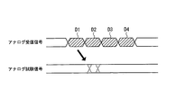
例えば、トランスポンダ式ATSでは、FSK(Frequency Shift Keying)方式を用いているため、制御信号の周波数帯域幅をバンドパスフィルタにて制限している場合がある。この場合、アナログ試験信号の周波数は、アナログ受信信号の周波数帯域外に設定することが困難である。
そこで、第3の実施形態では、アナログ試験信号の周波数をアナログ受信信号の周波数帯域内に設定し、信号の内容(電文)において区別する。例えば、アナログ試験信号の電文は、アナログ受信信号で使用され得ない(意味の無い)電文とし、アナログ受信信号の電文と必ず相違させる。より詳細には、アナログ試験信号の電文として、同一文字の羅列が考えられる。第3の実施形態の制御装置の構成は、第1または第2の実施形態の制御装置のいずれかの構成と同様でよい。
例えば、アナログ受信信号が受信されていない期間では、試験信号発生部50は、アナログ試験信号を間欠的に一定周期で出力する。制御部40a、40bは、第1または第2の実施形態と同様に、アナログ試験信号に対応するデジタル試験信号によってアナログ信号処理システムの健全性を確認することができる。
一方、アナログ受信信号が受信されている期間に、アナログ試験信号がアナログ受信信号に付加されると、アナログ受信信号の電文が復調できないおそれがある。しかし、通常、アナログ受信信号が送信される際には、同一内容の電文が連続して4つ送信される。制御部40a、40bは、連続した4つの電文のうち2つの電文が正確に復調できた場合にその電文を採用する。これは、4C2検定と呼ばれている。
そこで、4C2検定を利用して、アナログ試験信号と異なるアナログ受信信号の1つの電文が受信された場合、試験信号発生部50は、アナログ試験信号の発生を直ちに停止する。これにより、制御部40a、40bは、連続した4つの電文のうち少なくとも2つの電文が正確に復調できるようにする。もし、アナログ試験信号がアナログ受信信号の最初の電文に重複した場合には、その最初の電文は復調できないかもしれないが、その後の2~4番目の電文は復調可能である。もし、アナログ試験信号がアナログ受信信号の最初の電文に重複していない場合には、最初の電文を受信した後、直ちに、試験信号発生部50は、アナログ試験信号の発生を停止する。この場合、1~4番目の電文が全て復調可能である。
このように、第3の実施形態では、アナログ試験信号の周波数がアナログ受信信号の周波数帯域に重複するものの、データの内容(電文)においてアナログ試験信号とアナログ受信信号とを区別する。さらに、アナログ受信信号が受信された場合には、アナログ試験信号の発生を直ちに停止してアナログ受信信号の復調を可能にする。このように、第3の実施形態によれば、制御部40a、40bは、アナログ受信信号とアナログ試験信号の両方を復調可能とし、これらを識別することができる。これにより、アナログ信号処理システムの健全性を確認することができる。
本発明のいくつかの実施形態を説明したが、これらの実施形態は、例として提示したものであり、発明の範囲を限定することは意図していない。これら実施形態は、その他の様々な形態で実施されることが可能であり、発明の要旨を逸脱しない範囲で、種々の省略、置き換え、変更を行うことができる。これら実施形態やその変形は、発明の範囲や要旨に含まれると同様に、特許請求の範囲に記載された発明とその均等の範囲に含まれるものである。
Claims (11)
- アンテナを介して受信したアナログ受信信号を処理するアナログ信号処理部と、
前記アナログ信号処理部からのアナログ信号をデジタル信号へ変換するアナログ・デジタル変換部と、
前記デジタル信号を処理するデジタル信号処理部と、
前記デジタル信号処理部からの前記デジタル信号に基づいて電気車を制御する制御部と、
周波数または信号内容において前記アナログ受信信号と異なるアナログ試験信号を前記アナログ信号処理部に与える試験信号発生部と、を備えた電気車制御装置。 - 前記アナログ信号処理部および前記アナログ・デジタル変換部が正常である場合にアナログ試験信号の入力によって前記デジタル信号処理部から得られる正常デジタル試験信号を予め格納する記憶部をさらに備えた、請求項1に記載の電気車制御装置。
- 前記制御部は、前記アナログ試験信号の入力によって前記デジタル信号処理部から出力されるデジタル試験信号と前記正常デジタル試験信号とを比較し、その比較結果に応じて前記アナログ信号処理部および前記アナログ・デジタル変換部の異常を検知する、請求項2に記載の電気車制御装置。
- 前記試験信号発生部と前記アナログ信号処理部の入力との間に設けられた加算部をさらに備え、
前記加算部は、前記アナログ受信信号に前記アナログ試験信号を加算する、請求項1から請求項3のいずれか一項に記載の電気車制御装置。 - 前記アナログ試験信号のピーク周波数は、前記アナログ受信信号の周波数帯域の外側にある、請求項1から請求項4のいずれか一項に記載の電気車制御装置。
- 前記アナログ試験信号のピーク周波数は、前記アナログ受信信号の周波数帯域の近傍にあり、
前記アナログ受信信号の周波数帯域内における前記アナログ試験信号の強度は、前記アナログ受信信号のノイズレベル以下である、請求項5に記載の電気車制御装置。 - 前記アナログ試験信号のピーク周波数は、前記アナログ受信信号の周波数帯域の最大値を超える第1周波数と、前記アナログ受信信号の周波数帯域の最小値を下回る第2周波数とのいずれか一方または両方である、請求項5または請求項6に記載の電気車制御装置。
- 前記試験信号発生部は、前記ピーク周波数が前記第1周波数である前記アナログ試験信号と前記ピーク周波数が前記第2周波数である前記アナログ試験信号とを前記アナログ信号処理部へ交互に与える、請求項7に記載の電気車制御装置。
- 前記アナログ試験信号の信号強度は、前記アナログ受信信号の規格の下限近傍の第1信号強度と前記アナログ受信信号の規格の上限近傍の第2信号強度とを含む、請求項1から請求項8のいずれか一項に記載の電気車制御装置。
- 前記デジタル信号処理部は、前記デジタル信号が所定期間以上にわたって変化しない場合に、エラー信号を前記制御部へ出力し、
前記制御部は、前記エラー信号を受けた場合に前記アナログ信号処理部および前記アナログ・デジタル変換部が異常であると判断する、請求項1から請求項9のいずれか一項に記載の電気車制御装置。 - 前記試験信号発生部は、前記信号内容において前記アナログ受信信号と異なるアナログ試験信号の周波数を、前記アナログ受信信号の周波数帯域内に設定し、
前記信号内容によって前記アナログ受信信号が入力されたことを検知した場合、前記試験信号発生部は、前記アナログ試験信号の発生を停止する、請求項1から請求項10のいずれか一項に記載の電気車制御装置。
Priority Applications (1)
| Application Number | Priority Date | Filing Date | Title |
|---|---|---|---|
| CN201680036053.6A CN107709134B (zh) | 2015-07-01 | 2016-06-13 | 电车控制装置 |
Applications Claiming Priority (2)
| Application Number | Priority Date | Filing Date | Title |
|---|---|---|---|
| JP2015132887A JP6563716B2 (ja) | 2015-07-01 | 2015-07-01 | 電気車制御装置 |
| JP2015-132887 | 2015-07-01 |
Publications (1)
| Publication Number | Publication Date |
|---|---|
| WO2017002601A1 true WO2017002601A1 (ja) | 2017-01-05 |
Family
ID=57608686
Family Applications (1)
| Application Number | Title | Priority Date | Filing Date |
|---|---|---|---|
| PCT/JP2016/067594 Ceased WO2017002601A1 (ja) | 2015-07-01 | 2016-06-13 | 電気車制御装置 |
Country Status (3)
| Country | Link |
|---|---|
| JP (1) | JP6563716B2 (ja) |
| CN (1) | CN107709134B (ja) |
| WO (1) | WO2017002601A1 (ja) |
Families Citing this family (2)
| Publication number | Priority date | Publication date | Assignee | Title |
|---|---|---|---|---|
| CN108639103B (zh) * | 2018-04-12 | 2019-07-30 | 北京交通大学 | 轨道交通信号控制系统反应式故障-安全机制的实现方法 |
| JP7651449B2 (ja) * | 2021-12-28 | 2025-03-26 | 株式会社日立製作所 | 列車制御支援システム及び方法 |
Citations (5)
| Publication number | Priority date | Publication date | Assignee | Title |
|---|---|---|---|---|
| JP2006160161A (ja) * | 2004-12-09 | 2006-06-22 | Ntt Advanced Technology Corp | 地上子検出装置 |
| JP2008178230A (ja) * | 2007-01-19 | 2008-07-31 | Mitsubishi Electric Corp | 自動列車制御装置 |
| JP2008177680A (ja) * | 2007-01-16 | 2008-07-31 | Toshiba Corp | 無線機 |
| JP2009100506A (ja) * | 2007-10-15 | 2009-05-07 | Mitsubishi Electric Corp | 自動列車停止装置の車上用装置 |
| JP2014004991A (ja) * | 2012-05-29 | 2014-01-16 | Mitsubishi Electric Corp | 地上子情報読取装置 |
Family Cites Families (1)
| Publication number | Priority date | Publication date | Assignee | Title |
|---|---|---|---|---|
| WO2013162472A1 (en) * | 2012-04-23 | 2013-10-31 | Nanyang Technological University | Method and apparatus for detecting railway system defects |
-
2015
- 2015-07-01 JP JP2015132887A patent/JP6563716B2/ja active Active
-
2016
- 2016-06-13 CN CN201680036053.6A patent/CN107709134B/zh active Active
- 2016-06-13 WO PCT/JP2016/067594 patent/WO2017002601A1/ja not_active Ceased
Patent Citations (5)
| Publication number | Priority date | Publication date | Assignee | Title |
|---|---|---|---|---|
| JP2006160161A (ja) * | 2004-12-09 | 2006-06-22 | Ntt Advanced Technology Corp | 地上子検出装置 |
| JP2008177680A (ja) * | 2007-01-16 | 2008-07-31 | Toshiba Corp | 無線機 |
| JP2008178230A (ja) * | 2007-01-19 | 2008-07-31 | Mitsubishi Electric Corp | 自動列車制御装置 |
| JP2009100506A (ja) * | 2007-10-15 | 2009-05-07 | Mitsubishi Electric Corp | 自動列車停止装置の車上用装置 |
| JP2014004991A (ja) * | 2012-05-29 | 2014-01-16 | Mitsubishi Electric Corp | 地上子情報読取装置 |
Also Published As
| Publication number | Publication date |
|---|---|
| CN107709134A (zh) | 2018-02-16 |
| JP2017013649A (ja) | 2017-01-19 |
| JP6563716B2 (ja) | 2019-08-21 |
| CN107709134B (zh) | 2020-02-11 |
Similar Documents
| Publication | Publication Date | Title |
|---|---|---|
| KR102182528B1 (ko) | 레일 차량의 위치 신호를 생성하기 위한 온-보드 시스템 | |
| JP6563716B2 (ja) | 電気車制御装置 | |
| JP7078794B2 (ja) | 車上通信装置および鉄道車両 | |
| AU2013397474B2 (en) | Track circuit power supply vital monitor | |
| JPWO2011096568A1 (ja) | 車上トランスポンダ装置およびその健全性確認方法 | |
| WO2019111330A1 (ja) | 送信機、及び、タイヤ状態監視装置 | |
| JP2018007040A (ja) | 信号変換装置、処理装置、通信システムおよび信号変換方法 | |
| US9762374B1 (en) | Power line communication based monitoring system | |
| JP5364448B2 (ja) | 軌道回路用送信器 | |
| US20140323170A1 (en) | Method for considerably enhancing the availability of wireless connections | |
| JP6667723B2 (ja) | 列車位置測定システム、車上装置、および列車位置測定方法 | |
| JP2013197615A (ja) | 鉄道無線システム | |
| KR20180023483A (ko) | 철도 위치검지 시스템에서의 트랜스폰더 리더 및 그 제어방법 | |
| JP6483429B2 (ja) | 送信装置 | |
| JP5161158B2 (ja) | Atc送信器 | |
| US9882573B2 (en) | Method of fabricating electronic device and limit value setting apparatus | |
| JP5858713B2 (ja) | 列車位置検知システム | |
| JP2018198416A (ja) | 無線通信装置及び判定方法 | |
| JP2009117928A (ja) | 鉄道車両の運行時の無線妨害箇所の検出システム | |
| JP7651449B2 (ja) | 列車制御支援システム及び方法 | |
| JP2020077984A (ja) | 送信機異常検知装置 | |
| KR102931289B1 (ko) | 철도차량용 차상신호장치 자가진단 방법 | |
| JP6296462B2 (ja) | 車載制御装置 | |
| KR20140139197A (ko) | 철도신호용 제어장치 | |
| JP2012177660A (ja) | 二次監視レーダ装置及びそのデータ処理プログラム |
Legal Events
| Date | Code | Title | Description |
|---|---|---|---|
| 121 | Ep: the epo has been informed by wipo that ep was designated in this application |
Ref document number: 16817710 Country of ref document: EP Kind code of ref document: A1 |
|
| NENP | Non-entry into the national phase |
Ref country code: DE |
|
| 122 | Ep: pct application non-entry in european phase |
Ref document number: 16817710 Country of ref document: EP Kind code of ref document: A1 |