WO2017001823A1 - Method for preparing an organic semiconducting layer - Google Patents
Method for preparing an organic semiconducting layer Download PDFInfo
- Publication number
- WO2017001823A1 WO2017001823A1 PCT/GB2016/051848 GB2016051848W WO2017001823A1 WO 2017001823 A1 WO2017001823 A1 WO 2017001823A1 GB 2016051848 W GB2016051848 W GB 2016051848W WO 2017001823 A1 WO2017001823 A1 WO 2017001823A1
- Authority
- WO
- WIPO (PCT)
- Prior art keywords
- repeating units
- layer
- hole transporting
- groups
- interlayer
- Prior art date
- Legal status (The legal status is an assumption and is not a legal conclusion. Google has not performed a legal analysis and makes no representation as to the accuracy of the status listed.)
- Ceased
Links
Classifications
-
- C—CHEMISTRY; METALLURGY
- C08—ORGANIC MACROMOLECULAR COMPOUNDS; THEIR PREPARATION OR CHEMICAL WORKING-UP; COMPOSITIONS BASED THEREON
- C08G—MACROMOLECULAR COMPOUNDS OBTAINED OTHERWISE THAN BY REACTIONS ONLY INVOLVING UNSATURATED CARBON-TO-CARBON BONDS
- C08G61/00—Macromolecular compounds obtained by reactions forming a carbon-to-carbon link in the main chain of the macromolecule
- C08G61/12—Macromolecular compounds containing atoms other than carbon in the main chain of the macromolecule
-
- H—ELECTRICITY
- H10—SEMICONDUCTOR DEVICES; ELECTRIC SOLID-STATE DEVICES NOT OTHERWISE PROVIDED FOR
- H10K—ORGANIC ELECTRIC SOLID-STATE DEVICES
- H10K85/00—Organic materials used in the body or electrodes of devices covered by this subclass
- H10K85/10—Organic polymers or oligomers
- H10K85/111—Organic polymers or oligomers comprising aromatic, heteroaromatic, or aryl chains, e.g. polyaniline, polyphenylene or polyphenylene vinylene
-
- H—ELECTRICITY
- H10—SEMICONDUCTOR DEVICES; ELECTRIC SOLID-STATE DEVICES NOT OTHERWISE PROVIDED FOR
- H10K—ORGANIC ELECTRIC SOLID-STATE DEVICES
- H10K85/00—Organic materials used in the body or electrodes of devices covered by this subclass
- H10K85/10—Organic polymers or oligomers
- H10K85/111—Organic polymers or oligomers comprising aromatic, heteroaromatic, or aryl chains, e.g. polyaniline, polyphenylene or polyphenylene vinylene
- H10K85/115—Polyfluorene; Derivatives thereof
-
- H—ELECTRICITY
- H10—SEMICONDUCTOR DEVICES; ELECTRIC SOLID-STATE DEVICES NOT OTHERWISE PROVIDED FOR
- H10K—ORGANIC ELECTRIC SOLID-STATE DEVICES
- H10K85/00—Organic materials used in the body or electrodes of devices covered by this subclass
- H10K85/10—Organic polymers or oligomers
- H10K85/151—Copolymers
-
- C—CHEMISTRY; METALLURGY
- C08—ORGANIC MACROMOLECULAR COMPOUNDS; THEIR PREPARATION OR CHEMICAL WORKING-UP; COMPOSITIONS BASED THEREON
- C08G—MACROMOLECULAR COMPOUNDS OBTAINED OTHERWISE THAN BY REACTIONS ONLY INVOLVING UNSATURATED CARBON-TO-CARBON BONDS
- C08G2261/00—Macromolecular compounds obtained by reactions forming a carbon-to-carbon link in the main chain of the macromolecule
- C08G2261/10—Definition of the polymer structure
- C08G2261/14—Side-groups
- C08G2261/141—Side-chains having aliphatic units
- C08G2261/1412—Saturated aliphatic units
-
- C—CHEMISTRY; METALLURGY
- C08—ORGANIC MACROMOLECULAR COMPOUNDS; THEIR PREPARATION OR CHEMICAL WORKING-UP; COMPOSITIONS BASED THEREON
- C08G—MACROMOLECULAR COMPOUNDS OBTAINED OTHERWISE THAN BY REACTIONS ONLY INVOLVING UNSATURATED CARBON-TO-CARBON BONDS
- C08G2261/00—Macromolecular compounds obtained by reactions forming a carbon-to-carbon link in the main chain of the macromolecule
- C08G2261/10—Definition of the polymer structure
- C08G2261/14—Side-groups
- C08G2261/148—Side-chains having aromatic units
-
- C—CHEMISTRY; METALLURGY
- C08—ORGANIC MACROMOLECULAR COMPOUNDS; THEIR PREPARATION OR CHEMICAL WORKING-UP; COMPOSITIONS BASED THEREON
- C08G—MACROMOLECULAR COMPOUNDS OBTAINED OTHERWISE THAN BY REACTIONS ONLY INVOLVING UNSATURATED CARBON-TO-CARBON BONDS
- C08G2261/00—Macromolecular compounds obtained by reactions forming a carbon-to-carbon link in the main chain of the macromolecule
- C08G2261/30—Monomer units or repeat units incorporating structural elements in the main chain
- C08G2261/31—Monomer units or repeat units incorporating structural elements in the main chain incorporating aromatic structural elements in the main chain
- C08G2261/314—Condensed aromatic systems, e.g. perylene, anthracene or pyrene
- C08G2261/3142—Condensed aromatic systems, e.g. perylene, anthracene or pyrene fluorene-based, e.g. fluorene, indenofluorene, or spirobifluorene
-
- C—CHEMISTRY; METALLURGY
- C08—ORGANIC MACROMOLECULAR COMPOUNDS; THEIR PREPARATION OR CHEMICAL WORKING-UP; COMPOSITIONS BASED THEREON
- C08G—MACROMOLECULAR COMPOUNDS OBTAINED OTHERWISE THAN BY REACTIONS ONLY INVOLVING UNSATURATED CARBON-TO-CARBON BONDS
- C08G2261/00—Macromolecular compounds obtained by reactions forming a carbon-to-carbon link in the main chain of the macromolecule
- C08G2261/30—Monomer units or repeat units incorporating structural elements in the main chain
- C08G2261/31—Monomer units or repeat units incorporating structural elements in the main chain incorporating aromatic structural elements in the main chain
- C08G2261/316—Monomer units or repeat units incorporating structural elements in the main chain incorporating aromatic structural elements in the main chain bridged by heteroatoms, e.g. N, P, Si or B
- C08G2261/3162—Arylamines
-
- C—CHEMISTRY; METALLURGY
- C08—ORGANIC MACROMOLECULAR COMPOUNDS; THEIR PREPARATION OR CHEMICAL WORKING-UP; COMPOSITIONS BASED THEREON
- C08G—MACROMOLECULAR COMPOUNDS OBTAINED OTHERWISE THAN BY REACTIONS ONLY INVOLVING UNSATURATED CARBON-TO-CARBON BONDS
- C08G2261/00—Macromolecular compounds obtained by reactions forming a carbon-to-carbon link in the main chain of the macromolecule
- C08G2261/40—Polymerisation processes
- C08G2261/41—Organometallic coupling reactions
- C08G2261/411—Suzuki reactions
-
- C—CHEMISTRY; METALLURGY
- C08—ORGANIC MACROMOLECULAR COMPOUNDS; THEIR PREPARATION OR CHEMICAL WORKING-UP; COMPOSITIONS BASED THEREON
- C08G—MACROMOLECULAR COMPOUNDS OBTAINED OTHERWISE THAN BY REACTIONS ONLY INVOLVING UNSATURATED CARBON-TO-CARBON BONDS
- C08G2261/00—Macromolecular compounds obtained by reactions forming a carbon-to-carbon link in the main chain of the macromolecule
- C08G2261/50—Physical properties
- C08G2261/51—Charge transport
- C08G2261/512—Hole transport
-
- C—CHEMISTRY; METALLURGY
- C08—ORGANIC MACROMOLECULAR COMPOUNDS; THEIR PREPARATION OR CHEMICAL WORKING-UP; COMPOSITIONS BASED THEREON
- C08G—MACROMOLECULAR COMPOUNDS OBTAINED OTHERWISE THAN BY REACTIONS ONLY INVOLVING UNSATURATED CARBON-TO-CARBON BONDS
- C08G2261/00—Macromolecular compounds obtained by reactions forming a carbon-to-carbon link in the main chain of the macromolecule
- C08G2261/90—Applications
- C08G2261/95—Use in organic luminescent diodes
-
- H—ELECTRICITY
- H10—SEMICONDUCTOR DEVICES; ELECTRIC SOLID-STATE DEVICES NOT OTHERWISE PROVIDED FOR
- H10K—ORGANIC ELECTRIC SOLID-STATE DEVICES
- H10K50/00—Organic light-emitting devices
- H10K50/10—OLEDs or polymer light-emitting diodes [PLED]
- H10K50/14—Carrier transporting layers
- H10K50/15—Hole transporting layers
-
- H—ELECTRICITY
- H10—SEMICONDUCTOR DEVICES; ELECTRIC SOLID-STATE DEVICES NOT OTHERWISE PROVIDED FOR
- H10K—ORGANIC ELECTRIC SOLID-STATE DEVICES
- H10K71/00—Manufacture or treatment specially adapted for the organic devices covered by this subclass
- H10K71/40—Thermal treatment, e.g. annealing in the presence of a solvent vapour
- H10K71/421—Thermal treatment, e.g. annealing in the presence of a solvent vapour using coherent electromagnetic radiation, e.g. laser annealing
Definitions
- the present invention relates to a method for preparing an organic electronic device comprising the formation of a hole transporting interlayer using monomers which comprise polar groups.
- the invention is also concerned with polymers suitable for the formation of such interlayers as well as with organic electronic devices, in particular organic light emitting diodes, obtainable by the method of the invention.
- organic electronic devices were developed in large scale for various commercial applications, including innovative thin mobile devices, high- resolution displays, and photovoltaic cells.
- the new generation of devices must fulfil the requirements of being low-cost, lightweight and even flexible. It is also desired that said devices perform functions traditionally accomplished with much more expensive components based on conventional semiconductor materials, such as silicon.
- Organic electronic devices are based on small molecules and/or polymers, and include, for example, organic light-emitting devices (OLEDs), organic thin film transistors (OTFT), organic photovoltaic (OPV) devices and thermoelectric (TE) generators.
- OLEDs organic light-emitting devices
- OFT organic thin film transistors
- OCV organic photovoltaic
- TE thermoelectric
- Light emitting polymers possess a delocalised pi-electron system along the polymer backbone.
- the delocalised pi- electron system confers semiconducting properties to the polymer to provide the ability to support positive and negative charge carriers with high mobilities along the polymer chain.
- Thin films of these conjugated polymers can be used in the preparation of OLEDs. These devices have numerous advantages over devices prepared using conventional semiconducting materials, including the possibility of wide area displays, low DC working voltages and simplicity of manufacture. Devices of this type are described in, for example, WO-A-90/13148, U.S. Pat. No. 5,512,654 and WO-A- 95/06400.
- organic electroluminescent devices generally comprise an organic light emitting material which is positioned between a hole injecting electrode and an electron injecting electrode.
- the hole injecting electrode i.e. the anode
- ITO indium oxide
- the material commonly used for the electron injecting electrode (cathode) is a low work function metal such as calcium or aluminium.
- Typical device architectures are disclosed in, for example, WO-A-90/13148; U.S. Pat. No. 5,512,654; WO-A-95/06400; R. F. Service, Science 1998, 279, 1135; Wudl et al., Appi. Phys. Lett. 1998, 73, 2561 ; J. Bharathan, Y. Yang, Appl. Phys. Lett. 1998, 72, 2660; T. R. Hebner, C. C. Wu, D. Marcy, M. L. Lu, J. Sturm, Appl. Phys. Lett. 1998, 72, 519); and WO 99/48160.
- the injection of holes from the hole injecting layer such as ITO into the organic emissive layer is controlled by the energy difference between the hole injecting layer work function and the highest occupied molecular orbital (HOMO) of the emissive material, and the chemical interaction at the interface between the hole injecting layer and the emissive material.
- HOMO highest occupied molecular orbital
- the deposition of high work function organic materials on the hole injecting layer provides hole transporting interlayers (HTILs) which facilitate the hole injection into the light emitting layer, transport holes stably from the hole injecting electrode and obstruct electrons.
- PEDOT/PSS poly (styrene sulfonate)-doped poly (3,4-ethylene dioxythiophene)
- NBP N,N'-diphenyl-N,N'-(2-naphthyl)-(1 , 1 '-phenyl)-4,4'- diamine
- TPD hole transporting interlayers
- HTILs hole transporting interlayers
- hole transporting interlayers are known which are based on polymers which do contain olefinic crosslinking components attached to the polymeric backbone which comprise an active double bond, in combination with compounds such as benzocyclobutene derivatives. After depositing a polymer film comprising such units thermal crosslinking treatments are applied, usually at temperatures of about 170°C or more for 60 minutes or more.
- the cyclobutene rings thereby open to result in the formation of highly reactive dienes which then may react with the neighbouring olefin units in a Diels Alder [4+2] cycioaddition reaction.
- the obtained crosslinked polymer becomes insoluble, provides the desired interlayer function and allows for further deposition of the remaining layers to form the desired organic electronic device without any detrimental effect on teh interlayer.
- the present invention provides a polymer material suitable for interlayer formation which is characterized in that it comprises a repeating unit with polar groups provided on side chains. These polar groups allow for the preparation of polymeric materials, suitable for interlayer preparation, which may be crosslinked by a process requiring lower temperatures, compared with the prior art materials discussed above while still providing teh desired interlayer functionality.
- the polymer is specified in claim 1.
- the present invention also provides a method for preparing an organic electronic device utilizing such interlayer materials, typically comprising at least an anode layer, a hole transporting interlayer, a light emitting layer, and a cathode layer, the method comprising the steps of:
- the present invention also provides an organic electronic device comprising at least an anode layer, a hole transporting interlayer, a light emitting layer, and a cathode layer, said organic electronic device obtainable by the method of the present invention.
- Figure 1 illustrates the external quantum efficiency of a device in accordance with the present invention compared with two control devices representing the prior art.
- Figure 2 illustrates the operational lifetime of a device in accordance with the present invention compared with two control devices representing the prior art.
- semiconductor refers to a compound that can act as either an electrical conductor or insulator depending upon the voltage applied to it.
- semiconductor layer refers to a continuous film of material that is semiconducting.
- the semiconducting layer formed in the present invention comprises a mixture or blend of polymeric and non-polymeric semiconductor.
- the polymeric semiconductor forms a matrix in which the non-polymeric semiconductor is dispersed.
- polymeric semiconductor refers to polymeric compounds comprising repeating units that are semiconductors. Polymers usually have a polydispersity of greater than 1.
- non-polymeric semiconductor refers to small molecule compounds that are semiconductors.
- the term includes dendrimeric and oligomeric compounds (e.g. dimers, trimers, tetramers and pentamers) that have a polydispersity of 1.
- Preferred non-polymeric semiconductors are crystalline.
- lateral distribution refers to a distribution of non- polymeric semiconductor crystals which extend substantially the entire length of the channel between the source and the drain electrodes as well as over the source and drain electrodes, in a direction parallel to the surface of the electrodes.
- aromatic solvent refers to solvents comprising one or more compounds that comprise a planar ring that has 4n+2 pi electrons, wherein n is a non-negative integer.
- boiling point refers to the temperature at which boiling occurs at 1 atmosphere of pressure.
- alkyl refers to saturated, straight chained, branched or cyclic groups. Alkyl groups may be substituted or unsubstituted.
- alkenyl refers to unsaturated straight chained, branched or cyclic groups. Alkenyl groups may be substituted or unsubstituted.
- alkoxy refers to O-alkyl groups, wherein alkyl is as defined above.
- amino refers to primary (i.e. NH 2 ), secondary (NHR) and tertiary amino groups (NR 2 ) wherein R is alkyl as defined above.
- sil refers to groups of the formulae -A-SiR'R"R"' wherein A is optionally present and is a saturated or unsaturated group selected from C1-8 alkylene, Ci-e alkenylene or Ci-s alkynylene and each of R', R" and R'" is H or alkyl as defined above.
- stannyl refers to groups of the formulae -Sn(R') r wherein r is 1 , 2 or 3 and each R' is H or alkyl as defined above.
- halogen encompasses atoms selected from the group consisting of F, CI, Br and I.
- aryl includes single and multiple ring compounds, including multiple ring compounds that contain separate or fused rings.
- heteroaryl refers to aryl groups comprising a heteroatom selected from N, O and S.
- An example of an aryl group is phenyl, i.e. C6H5. Phenyl groups may be substituted or unsubstituted.
- An example of a heteroaryl group is thiophene, i.e. C4H4S. It may be substituted or unsubstituted.
- compositional ratios and % refer to the weight (i.e. define the wt.-% of a given component in a copolymer or blend).
- Polymeric materials suitable for interlayer formation typically do comprise repeating units responsible for hole transport, repeating units responsible for proving conjugation and/or conjugation break along the polymer backbone, and repeating units responsible for the post deposition crosslinking, in order to allow insolubilization of the deposited polymer layer.
- Repeating units known for providing hole transport are aromatic repeating units comprising tri-aryl amine groups.
- Repeating units proving conjugation and/or conjugation break known to the skilled person are repeating units based on aromatic compounds, preferably fluorine based compounds.
- Repeating units known in the art for providing functionalities for the post deposition crosslinking reactions are aromatic repeating units comprising cyclobutene units and aromatic units comprising side chains with (preferable terminal) olefinic moieties. While these materials have been used for the preparation of the respective layers in light emitting devices, the functionalities employed for post deposition crosslinking require the above described long treatment times and high temperatures.
- the novel polymer usable for the formation of hole transporting interlayers comprises repeating units responsible for hole transport as well as repeating units for providing conjugation and/or conjugation break, but does not comprise conventional repeating units responsible in the prior art for crosslinking of the polymer. These repeating units therefore do not comprise cycloalkene moieties and/or other olefinic moieties. Instead the novel materials provided by the present invention do comprise repeating units allowing for post deposition crosslinking selected among aromatic repeating units with side chains, preferably alkylene side chains, which do show a terminal polar group. Such polar groups as further defined herein do allow for post deposition crosslinking (by UV irradiation and temperature increase, requiring shorter treatment times and typically also lower treatment temperatures).
- the side chains on which the polar group as identified herein is provided are preferably alkylene side chains with 2 to 10, preferably 2 to 6, more preferably 2 to 4 carbon atoms.
- the side chain is a non-branched alkylene side chain.
- the polar groups used in accordance with the present invention may be selected among the group comprising amino groups, alkyl- or aryl amino groups, di- alkyl or di-aryl amino groups, mixed alkyl aryl amino groups, glycol groups, including polyethylene (PEG) and polypropylene glycol groups, ether and polyether groups, ketone and aldehyde moieties, carboxyl groups as well as carboxylic ester groups.
- a suitable aryl group to be used for the polar groups as defined herein is in particular a phenyl group, with further examples being aromatic units with two or more aromatic rings, which may be fused or connected in any other manner, such as naphthyl, fluorenyl, etc.
- these aryl groups do not show any further substituents, although it is possible for these aryl groups to have alkyl substituents, preferably with from 1 to 10, more preferably from 1 to 4 carbon atoms.
- Any group as identified above comprising an alkyl moiety preferably comprises an alkyl moiety with from 1 to 10 carbon atoms, preferably 1 to 5 carbon atoms. Examples are methyl, ethyl, propyl, iso- propyl, butyl, tert-butyl and pentyl groups.
- Examples of such polar groups are di-methyl or di-isopropyl amino groups, carboxylic acid ester groups (-COOR) with the R residue being an alkyl group as exemplified above, as well as ketone groups (-COR) with the R residue again being an alkyl group as illustrated above.
- Preferred are (terminal) amino, alkyl amino, and di-alkyl amino groups.
- Such a material may be prepared using standard polymerization techniques known in the art, yielding a polymeric material which, after synthesis and work-up still is soluble, can be deposited using solution based methods while allowing for a post deposition crosslinking requiring lower temperatures and reduced crosslinking processing time.
- the polymeric material provided by the present invention comprises repeating units responsible for hole transport, conjugation and/or conjugation break as well as for the crosslinking which are fluorine based repeating units.
- repeating units responsible for hole transport, conjugation and/or conjugation break as well as for the crosslinking which are fluorine based repeating units.
- polymerization technologies are known to the skilled person, allowing for the synthesis of the novel polymeric materials in a manner readily available to the skilled person, such as polymerization using metal catalysts. Suitable examples for such repeating units and respective monomers are illustrated in the examples.
- the repeating unit employed for the purpose of providing post deposition crosslinking is an aromatic repeating unit, preferable a fluorine based repeating unit, which does comprise side chains, preferable aliphatic side chains comprising terminal polar groups.
- the aliphatic side chains typically are alkylene side chains with 2 to 10, preferable 2 to 4 carbon atoms.
- each repeating unit comprises at least two of these side chain polar groups.
- the polar groups preferably are selected among dialkyl amino groups, wherein the alkyl groups have from 1 to 6 carbon atoms, preferable from 1 to 4 carbon atoms.
- a particularly preferred amino group is the dimethyl amino group.
- the amount of a repeating unit as described herein with side chains with (terminal) polar groups may be employed in the polymer in amounts of from 0.5 to 10 %, preferable 1 to 5 %.
- the polymeric material as defined herein may be crosslinked by a combination of a temperature treatment at temperatures not exceeding 170°C with UV irradiation. It has been found that crosslinking may be achieved with treatment times as short as 5 to 10 minutes, so that compared to the prior art conditions (thermal treatment of at least 170°C for 60 minutes or more) faster processing is achieved at lower overall temperatures.
- the present invention provides a method for preparing an organic electronic device comprising at least an anode layer, a hole transporting interlayer, a light emitting layer, and a cathode layer, the method comprising the steps of:
- a hole transporting interlayer of an organic electronic device is formed very fast with low annealing temperatures while allowing for similar initial device performance as compared to devices comprising standard interlayers known in the art.
- the annealing step of the deposited hole transporting interlayer in accordance with the present invention is advantageously carried out at a temperature of 160°C or below, preferably at a temperature of 150°C or below, and more preferably at a temperature of 140°C or below.
- the annealing temperature is preferably at least 100°C, more preferably at least 120°C.
- typical annealing temperatures are well above 170°C and are generally around 200°C.
- the annealing step of the deposited hole transporting interlayer in accordance with the present invention is preferably carried out for a time of less than 30 minutes, preferably 5 minutes or less, more preferably for a time of 4 minutes or less, and even more preferably for a time of 3 minutes or less.
- the annealing time is preferably at least 1 minute, more preferably at least 2 minutes.
- typical annealing times are typically 60 minutes and may at times be even longer.
- the solution for deposition of the hole transporting interlayer comprises a polymeric material as outlined above in a suitable solvent.
- suitable solvents are known to the skilled person.
- the annealing step of the method of the present invention can be carried out at lower temperatures and for shorter time periods in the presence of UV radiation. It has been found that a conventional annealing step, i.e. without UV irradiation does not provide the required insoiubilisation.
- the repeating units comprising the above polar groups also result in the advantage of the film formation not requiring any kind of crosslinking agent or crosslinking component, said crosslinking agent generally being required in the art and demanding higher annealing temperatures and annealing times.
- the solution for the deposition of the hole transporting layer does not comprise any crosslinking components which comprise non-aromatic double bonds.
- the solution for the deposition of the hole transporting layer does also not comprise any other components such as benzocyclobutene derivatives typically employed for the prior art crosslinking reactions.
- the present invention provides an organic electronic device comprising at least an anode layer, a hole transporting interlayer, a light emitting layer, and a cathode layer, said organic electronic device obtainable by the above method.
- the organic electronic device is an organic light emitting diode.
- a typical OLED geometry in accordance with the present invention includes
- a transparent conductive oxide anode for example an ITO anode
- the hole transporting interlayer also needs to display a high ionisation potential (i.e. a deep-HOMO level).
- the work function (WF) of the anode needs to be increased from around about 5.0 eV for native ITO to match the HOMO level in the hole transporting interlayer material.
- the surface of the ITO anode may preferably be covered with a thin layer of a p-doped conjugated polymer.
- HOMO and LUMO energy level values may generally be calculated by any method known to the skilled person in order to determine the energy levels required.
- a suitable measurement method is photoeiectron spectroscopy using AC-2 apparatus available from RK Instruments Inc. Measurements may alternatively be made using ultraviolet photoelectron spectroscopy measurements performed in a vacuum system, by irradiating the sample surface with ultraviolet light of a fixed wavelength. This measurement results in plots of the Photoelectron Intensity as a function of Kinetic Energy, which are 1 : 1-projections of the Density-Of-State in the sample substrate.
- HOMO levels of various organic compounds can also be found in, for example, Dekker, Handbook of Photophysics, 2 nd Edition, 993.
- the method of the present invention comprises the following further steps:
- the light emitting polymer is formed from the following monomers:
- the low work function metal forming the cathode being a bi- iayer or tri-iayer structure of metals or compounds selected from sodium fluoride, aluminium, calcium and silver.
- Deposition of the hole transporting interlayer is generally carried out from a solution. Any conventional solution-based processing method may be used. Representative examples of solution-based processing methods include spin coating, dip coating, slot die coating, doctor blade coating and ink-jet printing. In preferred methods of the invention, however, depositing is carried out by spin coating.
- the parameters used for spin coating the semiconductor film such as spin coating speed, acceleration and time are selected on the basis of the target thickness for the semiconducting layer. Typical target thicknesses are in the range of 20 to 60 nm.
- the spin coating is carried out in a single phase spin.
- the spin speed is 300 to 1000 rpm, more preferably 400 to 900 rpm and still more preferably 500 to 750 rpm.
- the spin time is 5 to 180 seconds, more preferably 10 to 60 seconds and still more preferably 20 to 40 seconds.
- the acceleration time from rest is less than 3 seconds, preferably less than 2 seconds and still more preferably less than 1 second.
- Any conventional spin coating apparatus may be used. The apparatus is used in a conventional manner.
- the material for the light emitting layer is a polymer, more preferably a conjugated polymer.
- the polymer is a polymeric semiconductor and comprises a repeat uni
- R 1 and R 2 are the same or different and each is selected from the group consisting of hydrogen, an alkyl group having from 1 to 16 carbon atoms, an aryl group having from 5 to 14 carbon atoms and a 5- to 7-membered heteroaryl group containing from 1 to 3 sulfur atoms, oxygen atoms and/or nitrogen atoms, said aryl group or heteroaryl group being unsubstituted or substituted with one or more substituents selected from an alkyl group having from 1 to 16 carbon atoms and an alkoxy group having from 1 to 16 carbon atoms.
- alkyl groups include methyl, ethyl, propyl, butyl, pentyl, hexyl, heptyl, octyl, nonyl or decyl.
- aryl groups include phenyl, indenyl, naphthyl, phenanthrenyl and anthracenyl groups.
- Examples of 5- to 7- membered heteroaryl groups include furyl, thienyl, pyrrolyl, azepinyl, pyrazolyl, imidazolyl, oxazolyl, isoxazolyl, thiazolyl, isothiazolyl, 1 ,2,3-oxadiazolyl, triazolyl, tetrazolyl, thiadiazolyl, pyranyl, pyridyl, pyridazinyl, pyrimidinyl and pyrazinyl groups.
- alkoxy groups include methoxy, ethoxy, propoxy, isopropoxy and butoxy.
- R 1 and R 2 are the same.
- Preferred polymers comprise a repeat unit of formula (Ilia) wherein, wherein R 1 and R 2 are each selected from the group consisting of hydrogen, an alkyl group having from 1 to 12 carbon atoms and a phenyl group, said phenyl group being unsubstituted or substituted with one or more substituents selected from an alkyl group having from 1 to 12 carbon atoms and an alkoxy group having from 1 to 12 carbon atoms.
- R 1 and R 2 are each selected from the group consisting of hydrogen, an alkyl group having from 1 to 12 carbon atoms and a phenyl group, said phenyl group being unsubstituted or substituted with one or more substituents selected from an alkyl group having from 1 to 12 carbon atoms and an alkoxy group having from 1 to 12 carbon atoms.
- Still more preferred polymeric semiconductors comprise a repeat unit of formula (I lia) wherein R 1 and R 2 are each selected from the group consisting of an alkyl group having from 4 to 12 carbon atoms and a phenyl group, said phenyl group being unsubstituted or substituted with one or more substituents selected from an alkyl group having from 4 to 8 carbon atoms and an alkoxy group having from 4 to 8 carbon atoms.
- Yet further preferred polymeric semiconductors comprise a repeat unit of formula (Ilia) wherein R 1 and R 2 are each selected from the group consisting of an alkyl group having from 4 to 12 carbon atoms, preferably butyl, pentyl, hexyl, heptyl, octyl, nonyl or decyl, particularly octyl, e.g. n-ocytyl.
- Ar 1 and Ar 2 are the same or different and each is selected from an aryl group having from 5 to 14 carbon atoms and a 5- to 7-membered heteroaryl group containing from 1 to 3 sulfur atoms, oxygen atoms and/or nitrogen atoms, said aryl group or heteroaryl group being unsubstituted or substituted with one or more substituents selected from an alkyl group having from 1 to 16 carbon atoms and an alkoxy group having from 1 to 16 carbon atoms;
- R 3 is an alkyl group having from 1 to 8 carbon atoms or a phenyl group which may be unsubstituted or substituted with an alkyl group having from 1 to 8 carbon atoms;
- n is an integer greater than or equal to 1 , preferably 1 or 2.
- aryl groups include phenyl, indenyl, naphthyl, phenanthrenyl and anthracenyl groups.
- 5- to 7- membered heteroaryl groups include furyl, thienyl, pyrrolyl, azepinyl, pyrazolyl, imidazolyl, oxazolyl, isoxazolyl, thiazolyl, isothiazolyl, 1 ,2,3-oxadiazolyl, triazolyl, tetrazolyl, thiadiazolyl, pyranyl, pyridyl, pyridazinyl, pyrimidinyl and pyrazinyl groups.
- alkyl groups include methyl, ethyl, propyl, butyl, pentyl, hexyl, heptyl, octyl, nonyl or decyl.
- alkoxy groups include methoxy, ethoxy, propoxy, isopropoxy and butoxy.
- Ar 1 and Ar 2 are the same. Particularly preferably each of Ar 1 and Ar 2 is a phenyl group, preferably an unsubstituted phenyl group.
- R 3 is an alkyl group having from 1 to 8 carbon atoms or a phenyl group which may be unsubstituted or substituted with an alkyl group having from 1 to 8 carbon atoms.
- R 3 is alkyl group, especially an alkyl group comprising 2 to 5 carbon atoms, e.g. ethyl, propyl, butyl, pentyl.
- R 3 is a phenyl group substituted with an alkyl group having from 1 to 8 carbon atoms, e. g. ethyl, propyl, butyl, pentyl.
- the polymer comprises a repeat unit of formula (Ilia) and a repeat unit of formula (1Mb).
- the ratio of repeat unit of formula (I) to formula (II) is in the range 3: 1 to 1 :3, more preferably 2: 1 to 1 :2 and still more preferably about 1 : 1.
- the polymeric semiconductor comprises a repeat unit of formula (lllc):
- R 1 , R 2 , Ar 1 , Ar 2 and R 3 are as defined above in relation to formulae (Ilia) and (1Mb).
- the polymer is TFB [9,9'-dioctylfluorene-co-N-(4- butylphenyl)-diphenylamine]n, wherein n is greater than 100.
- a non-polymeric material for the light emitting layer may be any small molecule semiconductor suitable for the purpose, e.g. those known to the skilled person skilled as described in the prior such as those small molecule semiconductors described in WO2010/061 176. Suitable non-polymeric materials are commercially available. Typical examples include pentacene derivatives and thiophene derivatives.
- hole transporting interlayer using monomers which comprise polar groups can be formed for organic electronic devices.
- the polar groups are attached to the monomers via flexible spacers and allow for the omission of crosslinking agents with active double bonds or other compounds with similar purpose such as benzocyclobutene derivatives.
- the improved process is solution-based, overcoming the scale-up problems associates with the methods known in the art so far, and allows for a more cost and time efficient production of organic electronic devices.
- Performances were compared for spin-coated Blue OLED pixels (1) without a hole transporting interlayer, (2) with 22 nm of a standard thermally crosslinked hole transporting interlayer (60 min at 170°C), and (3) with 22 nm of a hole transporting interlayer according to the invention, which was crosslinked in a UV- assisted annealing step for 2 minutes (UVGL-58 Lamp; 254nm, 6W).
- ITO anode/ 35 nm hole injection layer (HIL) / x nm IL / 65nm LEP (blue Light Emitting Polymer) / standard NaF-AI-Ag cathode x nm IL no IL; 22 nm interlayer polymer 3 (170°C / 60 min); and 22 nm interlayer polymer 4 (UV at 160°C / 2 min).
- HIL hole injection layer
- x nm IL / 65nm LEP blue Light Emitting Polymer
- the interlayers used in the experiment were formed as follows:
- Standard interlayer polymer 3 Conjugation-broken IL
- control devices with 22nm of standard interlayer polymer 3 hole transporting interlayer (crosslinked at 170°C/60 min) display a maximum averaged EQE of just below 10%, whereas the averaged maximum EQE of blue devices without a hole transporting interlayer is very low, at around 1 %.
- the external quantum efficiency is the ratio of electrons collected from a device to the number of photons incident on the device. Absolute values for the external quantum efficiency were measured with a calibrated integrating sphere.
- the control devices with 22nm of standard interlayer polymer 3 crosslinked at 170°C/60 min) display T90% lifetimes of approx. 180 hrs, when driven from 500Cd/m 2 initial luminance, with a standard decay shape.
- the hole transporting interlayer free devices display massive "bright waving", i.e. a fast initial luminance increase during the first hours of lifetime testing. Once the maximum of the bright wave is reached, the rate of decay then becomes much faster than in the control devices, resulting in T90% lifetimes of 258.6 hrs.
- the hole transporting interlayer free devices in the above experiment were driven from just 100Cd/m 2 initial luminance. Assuming a quadratic dependence of the lifetime on initial luminance, T90% lifetimes of just 10.3 hrs would be expected for the hypothetical case of driving the hole transporting interlayer free devices from 500Cd/m 2 initial luminance as for the control devices.
- the hole transporting interlayer in accordance with the present invention (crosslinked for 2 minutes under UV-illumination at 160°C) results in T90% lifetimes of approximately 19.5 hrs, when driven from 1000Cd/m 2 initial luminance. Again assuming a quadratic dependence of the lifetime on initial luminance, T90% lifetimes of around 78 hrs would be expected for the hypothetical case of driving devices with hole transporting interlayers in accordance with the present invention from 500Cd/m 2 initial luminance as for the control devices.
- the present invention provides an improved process which is solution-based, overcoming the scale-up problems associates with the methods known in the art so far, and allows for a more cost and time efficient production of organic electronic device being formed very fast with low annealing temperatures while allowing for similar initial device performance as compared to devices comprising standard interlayers known in the art.
Landscapes
- Chemical & Material Sciences (AREA)
- Engineering & Computer Science (AREA)
- Materials Engineering (AREA)
- Health & Medical Sciences (AREA)
- Chemical Kinetics & Catalysis (AREA)
- Medicinal Chemistry (AREA)
- Polymers & Plastics (AREA)
- Organic Chemistry (AREA)
- Electroluminescent Light Sources (AREA)
Abstract
A method for preparing an organic electronic device comprising at least an anode layer, a hole transporting interlayer, a light emitting layer, and a cathode layer, the method comprising the steps of:(i) depositing a hole transporting interlayer from a solution comprising a specific molecular architecture; and (ii) annealing said deposited layer by heating to a temperature of 160°C or below and exposing the deposited layer to UV radiation.
Description
METHOD FOR PREPARING AN ORGANIC SEMICONDUCTING LAYER
FIELD OF THE INVENTION
The present invention relates to a method for preparing an organic electronic device comprising the formation of a hole transporting interlayer using monomers which comprise polar groups. The invention is also concerned with polymers suitable for the formation of such interlayers as well as with organic electronic devices, in particular organic light emitting diodes, obtainable by the method of the invention. BACKGROUND
In recent years, organic electronic devices were developed in large scale for various commercial applications, including innovative thin mobile devices, high- resolution displays, and photovoltaic cells. The new generation of devices must fulfil the requirements of being low-cost, lightweight and even flexible. It is also desired that said devices perform functions traditionally accomplished with much more expensive components based on conventional semiconductor materials, such as silicon.
Organic electronic devices are based on small molecules and/or polymers, and include, for example, organic light-emitting devices (OLEDs), organic thin film transistors (OTFT), organic photovoltaic (OPV) devices and thermoelectric (TE) generators.
There has been considerable interest in light emitting organic materials, such as conjugated polymers, for a number of years. Light emitting polymers possess a delocalised pi-electron system along the polymer backbone. The delocalised pi- electron system confers semiconducting properties to the polymer to provide the ability to support positive and negative charge carriers with high mobilities along the polymer chain.
Thin films of these conjugated polymers can be used in the preparation of OLEDs. These devices have numerous advantages over devices prepared using conventional semiconducting materials, including the possibility of wide area displays, low DC working voltages and simplicity of manufacture. Devices of this type are described in, for example, WO-A-90/13148, U.S. Pat. No. 5,512,654 and WO-A- 95/06400.
Great efforts have been dedicated to the realization of a full-colour, all plastic screen. The major challenges to achieve this goal are: (1) access to conjugated polymers emitting light of the three basic colours red, green and blue; and (2) the
conjugated polymers must be easy to process and fabricate into full-colour display structures. OLEDs are effective in meeting the first requirement, since manipulation of the emission colour can be achieved by changing the chemical structure of the organic emissive compound.
However, while modulation of the chemical nature of the emissive layer is often relatively easy and inexpensive on the lab scale it can be an expensive and complicated process on the industrial scale. The second requirement of the easy processability and build-up of full colour matrix devices raises the question of how to micro-pattern fine multicolour pixels and how to achieve full-colour emission. Inkjet printing, hybrid Inkjet printing technology and spin coating are examples of suitable technologies that can be adopted to apply the polymer solutions in the desired pattern.
At their most basic, organic electroluminescent devices generally comprise an organic light emitting material which is positioned between a hole injecting electrode and an electron injecting electrode. The hole injecting electrode (i.e. the anode) is typically a transparent tin-doped indium oxide (ITO)-coated glass substrate. The material commonly used for the electron injecting electrode (cathode) is a low work function metal such as calcium or aluminium.
Typical device architectures are disclosed in, for example, WO-A-90/13148; U.S. Pat. No. 5,512,654; WO-A-95/06400; R. F. Service, Science 1998, 279, 1135; Wudl et al., Appi. Phys. Lett. 1998, 73, 2561 ; J. Bharathan, Y. Yang, Appl. Phys. Lett. 1998, 72, 2660; T. R. Hebner, C. C. Wu, D. Marcy, M. L. Lu, J. Sturm, Appl. Phys. Lett. 1998, 72, 519); and WO 99/48160.
The injection of holes from the hole injecting layer such as ITO into the organic emissive layer is controlled by the energy difference between the hole injecting layer work function and the highest occupied molecular orbital (HOMO) of the emissive material, and the chemical interaction at the interface between the hole injecting layer and the emissive material. The deposition of high work function organic materials on the hole injecting layer, such as poly (styrene sulfonate)-doped poly (3,4-ethylene dioxythiophene) (PEDOT/PSS), N,N'-diphenyl-N,N'-(2-naphthyl)-(1 , 1 '-phenyl)-4,4'- diamine (NBP) and N,N'-bis(3-methylphenyl)-1 , 1 '-biphenyl-4,4'-diamine (TPD), provides hole transporting interlayers (HTILs) which facilitate the hole injection into the light emitting layer, transport holes stably from the hole injecting electrode and obstruct electrons. These layers are effective in increasing the number of holes introduced into the light emitting layer. However, the surface of ITO is not well defined and the chemistry at the interface with these conventional hole transport materials is hard to control.
In the prior art, hole transporting interlayers are known which are based on polymers which do contain olefinic crosslinking components attached to the polymeric backbone which comprise an active double bond, in combination with compounds such as benzocyclobutene derivatives. After depositing a polymer film comprising such units thermal crosslinking treatments are applied, usually at temperatures of about 170°C or more for 60 minutes or more. In case of employing benzocyclobutene derivatives, the cyclobutene rings thereby open to result in the formation of highly reactive dienes which then may react with the neighbouring olefin units in a Diels Alder [4+2] cycioaddition reaction. The obtained crosslinked polymer becomes insoluble, provides the desired interlayer function and allows for further deposition of the remaining layers to form the desired organic electronic device without any detrimental effect on teh interlayer.
However, such crosslinking reactions occur at relatively high temperatures above 170°C, and require long annealing times, typically at least 60 minutes, which makes integration into roll-to-roll fabrication on flexible organic electronic devices on light weight plastic substrates difficult.
In view of the above, there is a need for an improved material suitable for the formation of interlayers, overcoming the scale-up problems associates with the methods known in the art as well as overcoming the temperature restrictions associated with the prior art technologies discussed above. Namely, such new materials should allow the use of solution based technologies for their deposition, while allowing for processes for rendering the material insoluble which do not interfere with the other layers already present. These new materials for the interlayers should however not interfere with the required functionality and allow integration into standard manufacturing processes of organic electronic devices. Preferably the new materials should allow for a solution based process and maintain the satisfactory interlayer function known from the interlayers based on olefinic crosslinking reactions mentioned above. This would allow for a more cost and time efficient production of organic electronic devices. There is also a need for organic electronic devices employing such materials as well as processes for producing organic electronic devices employing such nes interlayer materials.
SUMMARY OF INVENTION
Based on evaluations of known interlayer polymers which do comprise repeating units providing crosslinking functionalities by thermal treatment, i.e. the olefinic moieties and the cyclobutene moieties, the present invention provides a polymer material suitable for interlayer formation which is characterized in that it comprises a repeating unit with polar groups provided on side chains. These polar groups allow for the preparation of polymeric materials, suitable for interlayer preparation, which may be crosslinked by a process requiring lower temperatures, compared with the prior art materials discussed above while still providing teh desired interlayer functionality. The polymer is specified in claim 1.
The present invention also provides a method for preparing an organic electronic device utilizing such interlayer materials, typically comprising at least an anode layer, a hole transporting interlayer, a light emitting layer, and a cathode layer, the method comprising the steps of:
(i) depositing a hole transporting interlayer from a solution comprising repeating units which comprise polar groups on side chains; and
(ii) annealing said deposited layer by heating to a temperature of 160°C or below and exposing the deposited layer to UV radiation.
The present invention also provides an organic electronic device comprising at least an anode layer, a hole transporting interlayer, a light emitting layer, and a cathode layer, said organic electronic device obtainable by the method of the present invention.
Preferred embodiments are set forth in the sub-claims and the following detailed description.
BRIEF DESCRIPTION OF THE DRAWINGS
Figure 1 illustrates the external quantum efficiency of a device in accordance with the present invention compared with two control devices representing the prior art.
Figure 2 illustrates the operational lifetime of a device in accordance with the present invention compared with two control devices representing the prior art.
DEFINITIONS
As used herein the term "semiconductor" refers to a compound that can act as either an electrical conductor or insulator depending upon the voltage applied to it. The term "semiconducting layer" refers to a continuous film of material that is semiconducting. The semiconducting layer formed in the present invention comprises a mixture or blend of polymeric and non-polymeric semiconductor. Preferably the polymeric semiconductor forms a matrix in which the non-polymeric semiconductor is dispersed.
As used herein the term "polymeric semiconductor" refers to polymeric compounds comprising repeating units that are semiconductors. Polymers usually have a polydispersity of greater than 1.
As used herein the term "non-polymeric semiconductor" refers to small molecule compounds that are semiconductors. The term includes dendrimeric and oligomeric compounds (e.g. dimers, trimers, tetramers and pentamers) that have a polydispersity of 1. Preferred non-polymeric semiconductors are crystalline.
As used herein the term "lateral distribution" refers to a distribution of non- polymeric semiconductor crystals which extend substantially the entire length of the channel between the source and the drain electrodes as well as over the source and drain electrodes, in a direction parallel to the surface of the electrodes.
As used herein the term "aromatic solvent" refers to solvents comprising one or more compounds that comprise a planar ring that has 4n+2 pi electrons, wherein n is a non-negative integer.
As used herein the term "boiling point" refers to the temperature at which boiling occurs at 1 atmosphere of pressure.
As used herein the term "alkyl" refers to saturated, straight chained, branched or cyclic groups. Alkyl groups may be substituted or unsubstituted.
As used herein the term "alkenyl" refers to unsaturated straight chained, branched or cyclic groups. Alkenyl groups may be substituted or unsubstituted.
As used herein the term "alkoxy" refers to O-alkyl groups, wherein alkyl is as defined above.
As used herein the term "amino" refers to primary (i.e. NH2), secondary (NHR) and tertiary amino groups (NR2) wherein R is alkyl as defined above.
As used herein the term "amido" refers to groups of the formulae -NHCOR and -NRCOR wherein each R, which may the same or different, is alkyl as defined above.
As used herein the term "silyl" refers to groups of the formulae -A-SiR'R"R"' wherein A is optionally present and is a saturated or unsaturated group selected from
C1-8 alkylene, Ci-e alkenylene or Ci-s alkynylene and each of R', R" and R'" is H or alkyl as defined above.
As used herein the term "stannyl" refers to groups of the formulae -Sn(R')r wherein r is 1 , 2 or 3 and each R' is H or alkyl as defined above.
As used herein the term "halogen" encompasses atoms selected from the group consisting of F, CI, Br and I.
As used herein the term "aryl" includes single and multiple ring compounds, including multiple ring compounds that contain separate or fused rings. As used herein the term "heteroaryl" refers to aryl groups comprising a heteroatom selected from N, O and S. An example of an aryl group is phenyl, i.e. C6H5. Phenyl groups may be substituted or unsubstituted. An example of a heteroaryl group is thiophene, i.e. C4H4S. It may be substituted or unsubstituted.
If not defined otherwise herein all compositional ratios and % refer to the weight (i.e. define the wt.-% of a given component in a copolymer or blend).
DESCRIPTION OF THE INVENTION
Polymeric materials suitable for interlayer formation, i.e. for the preparation in particular of hole transporting interlayers, typically do comprise repeating units responsible for hole transport, repeating units responsible for proving conjugation and/or conjugation break along the polymer backbone, and repeating units responsible for the post deposition crosslinking, in order to allow insolubilization of the deposited polymer layer. Repeating units known for providing hole transport are aromatic repeating units comprising tri-aryl amine groups. Repeating units proving conjugation and/or conjugation break known to the skilled person are repeating units based on aromatic compounds, preferably fluorine based compounds. Repeating units known in the art for providing functionalities for the post deposition crosslinking reactions are aromatic repeating units comprising cyclobutene units and aromatic units comprising side chains with (preferable terminal) olefinic moieties. While these materials have been used for the preparation of the respective layers in light emitting devices, the functionalities employed for post deposition crosslinking require the above described long treatment times and high temperatures.
The novel polymer usable for the formation of hole transporting interlayers comprises repeating units responsible for hole transport as well as repeating units for providing conjugation and/or conjugation break, but does not comprise conventional repeating units responsible in the prior art for crosslinking of the polymer. These
repeating units therefore do not comprise cycloalkene moieties and/or other olefinic moieties. Instead the novel materials provided by the present invention do comprise repeating units allowing for post deposition crosslinking selected among aromatic repeating units with side chains, preferably alkylene side chains, which do show a terminal polar group. Such polar groups as further defined herein do allow for post deposition crosslinking (by UV irradiation and temperature increase, requiring shorter treatment times and typically also lower treatment temperatures).
The side chains on which the polar group as identified herein is provided are preferably alkylene side chains with 2 to 10, preferably 2 to 6, more preferably 2 to 4 carbon atoms. Preferably the side chain is a non-branched alkylene side chain.
The polar groups used in accordance with the present invention may be selected among the group comprising amino groups, alkyl- or aryl amino groups, di- alkyl or di-aryl amino groups, mixed alkyl aryl amino groups, glycol groups, including polyethylene (PEG) and polypropylene glycol groups, ether and polyether groups, ketone and aldehyde moieties, carboxyl groups as well as carboxylic ester groups. A suitable aryl group to be used for the polar groups as defined herein is in particular a phenyl group, with further examples being aromatic units with two or more aromatic rings, which may be fused or connected in any other manner, such as naphthyl, fluorenyl, etc. Typically these aryl groups do not show any further substituents, although it is possible for these aryl groups to have alkyl substituents, preferably with from 1 to 10, more preferably from 1 to 4 carbon atoms. Any group as identified above comprising an alkyl moiety, preferably comprises an alkyl moiety with from 1 to 10 carbon atoms, preferably 1 to 5 carbon atoms. Examples are methyl, ethyl, propyl, iso- propyl, butyl, tert-butyl and pentyl groups. Examples of such polar groups are di-methyl or di-isopropyl amino groups, carboxylic acid ester groups (-COOR) with the R residue being an alkyl group as exemplified above, as well as ketone groups (-COR) with the R residue again being an alkyl group as illustrated above. Preferred are (terminal) amino, alkyl amino, and di-alkyl amino groups. Such a material may be prepared using standard polymerization techniques known in the art, yielding a polymeric material which, after synthesis and work-up still is soluble, can be deposited using solution based methods while allowing for a post deposition crosslinking requiring lower temperatures and reduced crosslinking processing time.
In a preferred embodiment the polymeric material provided by the present invention comprises repeating units responsible for hole transport, conjugation and/or conjugation break as well as for the crosslinking which are fluorine based repeating units. For such repeating units polymerization technologies are known to the skilled
person, allowing for the synthesis of the novel polymeric materials in a manner readily available to the skilled person, such as polymerization using metal catalysts. Suitable examples for such repeating units and respective monomers are illustrated in the examples.
As identified above, the repeating unit employed for the purpose of providing post deposition crosslinking is an aromatic repeating unit, preferable a fluorine based repeating unit, which does comprise side chains, preferable aliphatic side chains comprising terminal polar groups. The aliphatic side chains typically are alkylene side chains with 2 to 10, preferable 2 to 4 carbon atoms. Preferably each repeating unit comprises at least two of these side chain polar groups. The polar groups preferably are selected among dialkyl amino groups, wherein the alkyl groups have from 1 to 6 carbon atoms, preferable from 1 to 4 carbon atoms. A particularly preferred amino group is the dimethyl amino group.
The amount of a repeating unit as described herein with side chains with (terminal) polar groups may be employed in the polymer in amounts of from 0.5 to 10 %, preferable 1 to 5 %.
Surprisingly it has been found that using such a molecular architecture (i.e. a polymer comprising repeating units responsible for hole transport, repeating units responsible for conjugation and/or conjugation break and repeating units as defined herein for providing the functionality of post deposition crosslinking, but nor comprising conventional olefin and cyclobutene based repeating units) allows the formation of a polymeric material which may be processed from solution and allows the formation of an insoluble layer (with hole transport functionality) requiring less detrimental crosslinking reactions. Namely, the polymeric material as defined herein may be crosslinked by a combination of a temperature treatment at temperatures not exceeding 170°C with UV irradiation. It has been found that crosslinking may be achieved with treatment times as short as 5 to 10 minutes, so that compared to the prior art conditions (thermal treatment of at least 170°C for 60 minutes or more) faster processing is achieved at lower overall temperatures.
By using the molecular architecture as outlined above it is furthermore possible to integrate a hole transport interlayer formation into the existing processes for the preparation of organic electronic devices, yielding devices with the desired functionally while being less demanding in relation to temperature induces problems due to the lower crosslinking temperatures and faster processing times enabled by the present invention.
In accordance therewith the present invention also provides the following.
The present invention provides a method for preparing an organic electronic device comprising at least an anode layer, a hole transporting interlayer, a light emitting layer, and a cathode layer, the method comprising the steps of:
(i) depositing a hole transporting interlayer from a solution comprising a polymeric material as described above; and
(ii) annealing said deposited layer by heating to a temperature of 160°C or below and exposing the deposited layer to UV radiation.
Advantageously, with the method of the present invention, a hole transporting interlayer of an organic electronic device is formed very fast with low annealing temperatures while allowing for similar initial device performance as compared to devices comprising standard interlayers known in the art.
The annealing step of the deposited hole transporting interlayer in accordance with the present invention is advantageously carried out at a temperature of 160°C or below, preferably at a temperature of 150°C or below, and more preferably at a temperature of 140°C or below. In order to provide complete annealing, the annealing temperature is preferably at least 100°C, more preferably at least 120°C. For comparison, in the prior art, typical annealing temperatures are well above 170°C and are generally around 200°C.
The annealing step of the deposited hole transporting interlayer in accordance with the present invention is preferably carried out for a time of less than 30 minutes, preferably 5 minutes or less, more preferably for a time of 4 minutes or less, and even more preferably for a time of 3 minutes or less. In order to provide complete annealing, the annealing time is preferably at least 1 minute, more preferably at least 2 minutes. For comparison, in the prior art, typical annealing times are typically 60 minutes and may at times be even longer.
Due to the annealing step of the hole transporting interlayer being carried out at comparatively low temperatures and for a short amount of time in the presence of UV radiation, integration into roll-to-roli fabrication on flexible organic electronic devices on light weight plastic substrates is achieved in a simple and cost effective manner.
The solution for deposition of the hole transporting interlayer comprises a polymeric material as outlined above in a suitable solvent. Suitable solvents are known to the skilled person.
Since the formation of the hole transporting interlayer is based on the presence of repeating units which comprise polar groups, the annealing step of the method of the present invention can be carried out at lower temperatures and for shorter time periods
in the presence of UV radiation. It has been found that a conventional annealing step, i.e. without UV irradiation does not provide the required insoiubilisation. The repeating units comprising the above polar groups also result in the advantage of the film formation not requiring any kind of crosslinking agent or crosslinking component, said crosslinking agent generally being required in the art and demanding higher annealing temperatures and annealing times. Thus, the solution for the deposition of the hole transporting layer does not comprise any crosslinking components which comprise non-aromatic double bonds. The solution for the deposition of the hole transporting layer does also not comprise any other components such as benzocyclobutene derivatives typically employed for the prior art crosslinking reactions.
In a further embodiment, the present invention provides an organic electronic device comprising at least an anode layer, a hole transporting interlayer, a light emitting layer, and a cathode layer, said organic electronic device obtainable by the above method. Preferably, the organic electronic device is an organic light emitting diode.
A typical OLED geometry in accordance with the present invention includes
- a transparent conductive oxide anode (for example an ITO anode),
- optionally a hole injection layer,
- a hole transporting interlayer,
- a light emitting layer,
- a cathode.
Efficient hole injection into the light emitting layer requires the band offset between the hole transporting interlayer and the light emitting to be small. As a consequence of this requirement, in the case of deep-HOMO materials employed in the light emitting layer, the hole transporting interlayer also needs to display a high ionisation potential (i.e. a deep-HOMO level). In order to enable hole injection from the anode into deep-HOMO hole transporting interlayer materials, the work function (WF) of the anode needs to be increased from around about 5.0 eV for native ITO to match the HOMO level in the hole transporting interlayer material. In order to match the WF of the ITO anode to the HOMO level in the hole transporting interlayer material, the surface of the ITO anode may preferably be covered with a thin layer of a p-doped conjugated polymer.
HOMO and LUMO energy level values may generally be calculated by any method known to the skilled person in order to determine the energy levels required. A suitable measurement method is photoeiectron spectroscopy using AC-2 apparatus available from RK Instruments Inc. Measurements may alternatively be made using
ultraviolet photoelectron spectroscopy measurements performed in a vacuum system, by irradiating the sample surface with ultraviolet light of a fixed wavelength. This measurement results in plots of the Photoelectron Intensity as a function of Kinetic Energy, which are 1 : 1-projections of the Density-Of-State in the sample substrate. HOMO levels of various organic compounds can also be found in, for example, Dekker, Handbook of Photophysics, 2nd Edition, 993.
in a more preferred embodiment, the method of the present invention comprises the following further steps:
- depositing a solution of a light emitting polymer on the top of the hole transporting interlayer;
- drying said layer of light emitting polymer to give a light emitting polymer layer; and
- thermally evaporating a material such as a low work function metal onto the light emitting polymer layer formed in the afore-mentioned step to form a cathode, thus giving the desired organic light emitting device;
Preferably, the light emitting polymer is formed from the following monomers:

Also preferred is the low work function metal forming the cathode being a bi- iayer or tri-iayer structure of metals or compounds selected from sodium fluoride, aluminium, calcium and silver.
Deposition of the hole transporting interlayer is generally carried out from a solution. Any conventional solution-based processing method may be used. Representative examples of solution-based processing methods include spin coating, dip coating, slot die coating, doctor blade coating and ink-jet printing. In preferred methods of the invention, however, depositing is carried out by spin coating. The parameters used for spin coating the semiconductor film such as spin coating speed,
acceleration and time are selected on the basis of the target thickness for the semiconducting layer. Typical target thicknesses are in the range of 20 to 60 nm. Preferably the spin coating is carried out in a single phase spin. Preferably the spin speed is 300 to 1000 rpm, more preferably 400 to 900 rpm and still more preferably 500 to 750 rpm. Preferably the spin time is 5 to 180 seconds, more preferably 10 to 60 seconds and still more preferably 20 to 40 seconds. Preferably the acceleration time from rest is less than 3 seconds, preferably less than 2 seconds and still more preferably less than 1 second. Any conventional spin coating apparatus may be used. The apparatus is used in a conventional manner.
Preferably the material for the light emitting layer is a polymer, more preferably a conjugated polymer. Preferably the polymer is a polymeric semiconductor and comprises a repeat uni

wherein R1 and R2 are the same or different and each is selected from the group consisting of hydrogen, an alkyl group having from 1 to 16 carbon atoms, an aryl group having from 5 to 14 carbon atoms and a 5- to 7-membered heteroaryl group containing from 1 to 3 sulfur atoms, oxygen atoms and/or nitrogen atoms, said aryl group or heteroaryl group being unsubstituted or substituted with one or more substituents selected from an alkyl group having from 1 to 16 carbon atoms and an alkoxy group having from 1 to 16 carbon atoms.
Examples of alkyl groups include methyl, ethyl, propyl, butyl, pentyl, hexyl, heptyl, octyl, nonyl or decyl. Examples of aryl groups include phenyl, indenyl, naphthyl, phenanthrenyl and anthracenyl groups. Examples of 5- to 7- membered heteroaryl groups include furyl, thienyl, pyrrolyl, azepinyl, pyrazolyl, imidazolyl, oxazolyl, isoxazolyl, thiazolyl, isothiazolyl, 1 ,2,3-oxadiazolyl, triazolyl, tetrazolyl, thiadiazolyl, pyranyl, pyridyl, pyridazinyl, pyrimidinyl and pyrazinyl groups. Examples of alkoxy groups include methoxy, ethoxy, propoxy, isopropoxy and butoxy.
In preferred polymeric semiconductors R1 and R2 are the same.
Preferred polymers comprise a repeat unit of formula (Ilia) wherein, wherein R1 and R2 are each selected from the group consisting of hydrogen, an alkyl group having from 1 to 12 carbon atoms and a phenyl group, said phenyl group being unsubstituted
or substituted with one or more substituents selected from an alkyl group having from 1 to 12 carbon atoms and an alkoxy group having from 1 to 12 carbon atoms. Still more preferred polymeric semiconductors comprise a repeat unit of formula (I lia) wherein R1 and R2 are each selected from the group consisting of an alkyl group having from 4 to 12 carbon atoms and a phenyl group, said phenyl group being unsubstituted or substituted with one or more substituents selected from an alkyl group having from 4 to 8 carbon atoms and an alkoxy group having from 4 to 8 carbon atoms. Yet further preferred polymeric semiconductors comprise a repeat unit of formula (Ilia) wherein R1 and R2 are each selected from the group consisting of an alkyl group having from 4 to 12 carbon atoms, preferably butyl, pentyl, hexyl, heptyl, octyl, nonyl or decyl, particularly octyl, e.g. n-ocytyl.
Further preferred polymers comprise a repeat unit of formula (lllb):

R3 is an alkyl group having from 1 to 8 carbon atoms or a phenyl group which may be unsubstituted or substituted with an alkyl group having from 1 to 8 carbon atoms;
and n is an integer greater than or equal to 1 , preferably 1 or 2.
Examples of aryl groups include phenyl, indenyl, naphthyl, phenanthrenyl and anthracenyl groups. Examples of 5- to 7- membered heteroaryl groups include furyl, thienyl, pyrrolyl, azepinyl, pyrazolyl, imidazolyl, oxazolyl, isoxazolyl, thiazolyl, isothiazolyl, 1 ,2,3-oxadiazolyl, triazolyl, tetrazolyl, thiadiazolyl, pyranyl, pyridyl, pyridazinyl, pyrimidinyl and pyrazinyl groups. Examples of alkyl groups include methyl, ethyl, propyl, butyl, pentyl, hexyl, heptyl, octyl, nonyl or decyl. Examples of alkoxy groups include methoxy, ethoxy, propoxy, isopropoxy and butoxy.
In preferred polymers comprising a repeat unit of formula (1Mb) Ar1 and Ar2 are the same. Particularly preferably each of Ar1 and Ar2 is a phenyl group, preferably an unsubstituted phenyl group.
In further preferred polymers comprising a repeat unit of formula (1Mb) R3 is an alkyl group having from 1 to 8 carbon atoms or a phenyl group which may be unsubstituted or substituted with an alkyl group having from 1 to 8 carbon atoms. Particularly preferably R3 is alkyl group, especially an alkyl group comprising 2 to 5 carbon atoms, e.g. ethyl, propyl, butyl, pentyl. Still more preferably R3 is a phenyl group substituted with an alkyl group having from 1 to 8 carbon atoms, e. g. ethyl, propyl, butyl, pentyl.
Still more preferably the polymer comprises a repeat unit of formula (Ilia) and a repeat unit of formula (1Mb). Preferably the ratio of repeat unit of formula (I) to formula (II) is in the range 3: 1 to 1 :3, more preferably 2: 1 to 1 :2 and still more preferably about 1 : 1. Particularly preferably the polymeric semiconductor comprises a repeat unit of formula (lllc):

Yet more preferably the polymer is TFB [9,9'-dioctylfluorene-co-N-(4- butylphenyl)-diphenylamine]n, wherein n is greater than 100.
A non-polymeric material for the light emitting layer may be any small molecule semiconductor suitable for the purpose, e.g. those known to the skilled person skilled as described in the prior such as those small molecule semiconductors described in WO2010/061 176. Suitable non-polymeric materials are commercially available. Typical examples include pentacene derivatives and thiophene derivatives.
Advantageously, with the method of the present invention, hole transporting interlayer using monomers which comprise polar groups can be formed for organic electronic devices. The polar groups are attached to the monomers via flexible spacers and allow for the omission of crosslinking agents with active double bonds or
other compounds with similar purpose such as benzocyclobutene derivatives. The improved process is solution-based, overcoming the scale-up problems associates with the methods known in the art so far, and allows for a more cost and time efficient production of organic electronic devices.
In the following, the invention will be further illustrated on the basis of examples.
EXAMPLES
Example 1
Performances were compared for spin-coated Blue OLED pixels (1) without a hole transporting interlayer, (2) with 22 nm of a standard thermally crosslinked hole transporting interlayer (60 min at 170°C), and (3) with 22 nm of a hole transporting interlayer according to the invention, which was crosslinked in a UV- assisted annealing step for 2 minutes (UVGL-58 Lamp; 254nm, 6W).
The following OLED device structures were used:
Standard blue-emitting devices fabricated by spin-coating in a glove box, with:
ITO anode/ 35 nm hole injection layer (HIL) / x nm IL / 65nm LEP (blue Light Emitting Polymer) / standard NaF-AI-Ag cathode x nm IL = no IL; 22 nm interlayer polymer 3 (170°C / 60 min); and 22 nm interlayer polymer 4 (UV at 160°C / 2 min).
The interlayers used in the experiment were formed as follows:
1) Standard interlayer polymer 3: Conjugation-broken IL
50% monomer 1 40% monomer 2 + 5% monomer 3 + 5% monomer 4
UV-crosslinked interlayer polymer 4: Conjugated IL
50% monomer 5 17.5% monomer 5 + 30% monomer 6 + 2.5% monomer 7
Monomers used in the ILs:
monomer 1 :

monomer 2: Amine Hole Transport Unit

monomer 3: BCB component

- monomer 4 Olefin component

- monomer 7: Fluorene with Dimethylamino groups
 - External Quantum Efficiency
As illustrated in Figure 1 , the control devices with 22nm of standard interlayer polymer 3 hole transporting interlayer (crosslinked at 170°C/60 min) display a maximum averaged EQE of just below 10%, whereas the averaged maximum EQE of blue devices without a hole transporting interlayer is very low, at around 1 %.
The external quantum efficiency is the ratio of electrons collected from a device to the number of photons incident on the device. Absolute values for the external quantum efficiency were measured with a calibrated integrating sphere.
By contrast, introducing the new interlayer polymer 4 (crosslinked for 2 minutes under UV-illumination at 160°C) in accordance with the present invention results in a maximum averaged EQE of around 7%.
The experiment shows that OLEDs produced with a fast-cured hole transporting interlayer in accordance with the present invention display much better EQEs than hole transporting interlayer free devices.
- Operational Lifetime
As illustrated in Figure 2, lifetime traces for hole transporting interlayer free devices are shown and compared to devices with standard interlayer polymer 3 and hole transporting interlayers in accordance with the present invention, all normalised at t = 6 min. The control devices with 22nm of standard interlayer polymer 3 (crosslinked at 170°C/60 min) display T90% lifetimes of approx. 180 hrs, when driven from 500Cd/m2 initial luminance, with a standard decay shape. In stark contrast to this, the hole transporting interlayer free devices display massive "bright waving", i.e. a fast initial luminance increase during the first hours of lifetime testing. Once the maximum of the bright wave is reached, the rate of decay then becomes much faster than in the control devices, resulting in T90% lifetimes of 258.6 hrs.
In addition, due to their very low EQEs, the hole transporting interlayer free devices in the above experiment were driven from just 100Cd/m2 initial luminance. Assuming a quadratic dependence of the lifetime on initial luminance, T90% lifetimes of just 10.3 hrs would be expected for the hypothetical case of driving the hole transporting interlayer free devices from 500Cd/m2 initial luminance as for the control devices.
The hole transporting interlayer in accordance with the present invention (crosslinked for 2 minutes under UV-illumination at 160°C) results in T90% lifetimes of approximately 19.5 hrs, when driven from 1000Cd/m2 initial luminance. Again assuming a quadratic dependence of the lifetime on initial luminance, T90% lifetimes of
around 78 hrs would be expected for the hypothetical case of driving devices with hole transporting interlayers in accordance with the present invention from 500Cd/m2 initial luminance as for the control devices.

This experiment shows that for the same initial luminance conditions, OLEDs with fast- cured IL600 are expected to display much better lifetimes than IL-free devices.
The present invention provides an improved process which is solution-based, overcoming the scale-up problems associates with the methods known in the art so far, and allows for a more cost and time efficient production of organic electronic device being formed very fast with low annealing temperatures while allowing for similar initial device performance as compared to devices comprising standard interlayers known in the art.
Claims
1 . A polymer usable for the formation of hole transporting interlayers comprising repeating units responsible for hole transport as well as repeating units for providing conjugation and/or conjugation break, and comprising repeating units allowing for post deposition crosslinking selected among aromatic repeating units with side chains, preferably alkylene side chains, which side chains have a terminal polar group selected from the group consisting of: amino groups, alkyl- or aryl amino groups, di-alkyl or di- aryl amino groups, mixed alkyl aryl amino groups, polyether groups, ketone and aldehyde moieties, and carboxyl groups.
2. A polymer according to claim 1 , not comprising aromatic repeating units comprising cyclobutene units and aromatic units comprising side chains with (preferable terminal) olefinic moieties.
3. A polymer according to claim 1 or claim 2, wherein the repeating units responsible for hole transport as well as repeating units for providing conjugation and/or conjugation break are fluorene based repeating units.
4. A polymer according to any one of claims 1 to 3, wherein the repeating units allowing for post deposition crosslinking are fluorene based repeating units.
5. Polymer according to any one of claims 1 to 4, comprising repeating units based upon any one of the following structures:
Fluorene backbone (conjugation break)
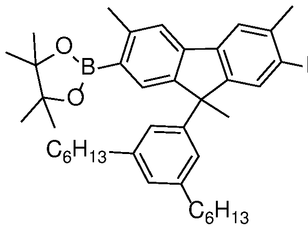


Fluorene with Dimethylamino groups

6. A method for preparing an organic electronic device comprising at least an anode layer, a hole transporting interlayer, a light emitting layer, and a cathode layer, the method comprising the steps of:
(i) depositing a hole transporting interlayer from a solution comprising a polymeric material as defined in any of the preceding claims; and
(ii) annealing said deposited layer by heating to a temperature of 160°C or below and exposing the deposited layer to UV radiation.
7. The method of claim 6, wherein the annealing step of the deposited layer is carried out at a temperature of 150 °C or below.
8. The method of claim 6 or 7, wherein the annealing step is carried out for a time period of 5 minutes or less.
9. The method of any of claims 6 to 8, wherein the annealing step is carried out for a time period of 3 minutes or less.
10. An organic electronic device comprising at least an anode layer, a hole transporting layer, a light emitting layer, and a cathode layer, the hole transport layer consisting of or including a polymeric material according to any one of claim 1 to 5.
1 1 . The organic electronic device of claim 10, wherein said organic electronic device is an organic light emitting diode.
Applications Claiming Priority (2)
| Application Number | Priority Date | Filing Date | Title |
|---|---|---|---|
| GBGB1511398.8A GB201511398D0 (en) | 2015-06-30 | 2015-06-30 | Method for preparing an organic semiconducting layer |
| GB1511398.8 | 2015-06-30 |
Publications (1)
| Publication Number | Publication Date |
|---|---|
| WO2017001823A1 true WO2017001823A1 (en) | 2017-01-05 |
Family
ID=53872390
Family Applications (1)
| Application Number | Title | Priority Date | Filing Date |
|---|---|---|---|
| PCT/GB2016/051848 Ceased WO2017001823A1 (en) | 2015-06-30 | 2016-06-21 | Method for preparing an organic semiconducting layer |
Country Status (2)
| Country | Link |
|---|---|
| GB (1) | GB201511398D0 (en) |
| WO (1) | WO2017001823A1 (en) |
Cited By (2)
| Publication number | Priority date | Publication date | Assignee | Title |
|---|---|---|---|---|
| US12048236B2 (en) | 2018-10-12 | 2024-07-23 | Corning Incorporated | UV patternable polymer blends for organic thin-film transistors |
| US12052911B2 (en) | 2018-11-05 | 2024-07-30 | Corning Incorporated | UV patternable polymer blends for organic thin-film transistors |
Citations (5)
| Publication number | Priority date | Publication date | Assignee | Title |
|---|---|---|---|---|
| WO2005049689A2 (en) * | 2003-11-17 | 2005-06-02 | Sumitomo Chemical Company, Limited | Crosslinkable substituted fluorene compounds and conjugated oligomers or polymers based thereon |
| WO2005052027A1 (en) * | 2003-11-17 | 2005-06-09 | Sumitomo Chemical Company, Limited | Crosslinkable arylamine compounds and conjugated oligomers of polymers based thereon |
| WO2010079330A1 (en) * | 2009-01-12 | 2010-07-15 | Cambridge Display Technology Limited | Interlayer formulation for flat films |
| WO2013013754A1 (en) * | 2011-07-25 | 2013-01-31 | Merck Patent Gmbh | Copolymers with functionalized side chains |
| WO2014102543A2 (en) * | 2012-12-24 | 2014-07-03 | Cambridge Display Technology Limited | Polymer and device |
-
2015
- 2015-06-30 GB GBGB1511398.8A patent/GB201511398D0/en not_active Ceased
-
2016
- 2016-06-21 WO PCT/GB2016/051848 patent/WO2017001823A1/en not_active Ceased
Patent Citations (5)
| Publication number | Priority date | Publication date | Assignee | Title |
|---|---|---|---|---|
| WO2005049689A2 (en) * | 2003-11-17 | 2005-06-02 | Sumitomo Chemical Company, Limited | Crosslinkable substituted fluorene compounds and conjugated oligomers or polymers based thereon |
| WO2005052027A1 (en) * | 2003-11-17 | 2005-06-09 | Sumitomo Chemical Company, Limited | Crosslinkable arylamine compounds and conjugated oligomers of polymers based thereon |
| WO2010079330A1 (en) * | 2009-01-12 | 2010-07-15 | Cambridge Display Technology Limited | Interlayer formulation for flat films |
| WO2013013754A1 (en) * | 2011-07-25 | 2013-01-31 | Merck Patent Gmbh | Copolymers with functionalized side chains |
| WO2014102543A2 (en) * | 2012-12-24 | 2014-07-03 | Cambridge Display Technology Limited | Polymer and device |
Cited By (2)
| Publication number | Priority date | Publication date | Assignee | Title |
|---|---|---|---|---|
| US12048236B2 (en) | 2018-10-12 | 2024-07-23 | Corning Incorporated | UV patternable polymer blends for organic thin-film transistors |
| US12052911B2 (en) | 2018-11-05 | 2024-07-30 | Corning Incorporated | UV patternable polymer blends for organic thin-film transistors |
Also Published As
| Publication number | Publication date |
|---|---|
| GB201511398D0 (en) | 2015-08-12 |
Similar Documents
| Publication | Publication Date | Title |
|---|---|---|
| JP5355857B2 (en) | An electronic device comprising an organic conductor and a semiconductor and an intermediate buffer layer made of a crosslinked polymer | |
| Zuniga et al. | Approaches to solution-processed multilayer organic light-emitting diodes based on cross-linking | |
| Hwang et al. | Conjugated polymers based on phenothiazine and fluorene in light-emitting diodes and field effect transistors | |
| JP5096378B2 (en) | Organic electronic device, manufacturing method thereof and use thereof | |
| Nuyken et al. | Modern trends in organic light-emitting devices (OLEDs) | |
| EP2335299B1 (en) | Derivatized fullerene-based dopants for organic semiconductors | |
| JP2015057785A (en) | Optical device | |
| Dey et al. | Diazirine-based photo-crosslinkers for defect free fabrication of solution processed organic light-emitting diodes | |
| WO2013064792A1 (en) | Organic electronic device and method of manufacture | |
| KR20170015182A (en) | Method of doping an organic semiconductor and doping composition | |
| Liguori et al. | Study of the electroluminescence of highly stereoregular poly (N-pentenyl-carbazole) for blue and white OLEDs | |
| Zhang et al. | Facile brush-coated β-phase poly (9, 9-dioctylfluorene) films for efficient and stable pure-blue polymer light-emitting diodes | |
| Song et al. | Emission color tuning of copolymers containing polyfluorene, benzothiadiazole, porphyrin derivatives | |
| Cun et al. | Modifying the organic/metal interface via solvent vapor annealing to enhance the performance of blue OLEDs | |
| US20080197768A1 (en) | Light Emissive Device | |
| EP3419968A1 (en) | Compound, composition and organic light-emitting device | |
| KR102466243B1 (en) | Organic light-emitting composition, device and method | |
| WO2017001823A1 (en) | Method for preparing an organic semiconducting layer | |
| US20080303432A1 (en) | Systems and methods for improving the qualities of polymer light-emitting electrochemical cells | |
| JP2011018922A (en) | Optical device | |
| Hu et al. | Polymer network hole transport layers based on photochemically cross-linkable N′ N′-diallyl amide tri-N-substituted triazatruxene monomers | |
| GB2483629A (en) | Light-emitting polymer and triplet-accepting unit | |
| CN104205396B (en) | Organic electroluminescence element and its manufacturing method | |
| EP1829129B1 (en) | Light emissive device | |
| WO2020002912A1 (en) | Phosphorescent light-emitting compound |
Legal Events
| Date | Code | Title | Description |
|---|---|---|---|
| 121 | Ep: the epo has been informed by wipo that ep was designated in this application |
Ref document number: 16732698 Country of ref document: EP Kind code of ref document: A1 |
|
| NENP | Non-entry into the national phase |
Ref country code: DE |
|
| 122 | Ep: pct application non-entry in european phase |
Ref document number: 16732698 Country of ref document: EP Kind code of ref document: A1 |