WO2016208405A1 - 撮像装置および撮像方法 - Google Patents
撮像装置および撮像方法 Download PDFInfo
- Publication number
- WO2016208405A1 WO2016208405A1 PCT/JP2016/067194 JP2016067194W WO2016208405A1 WO 2016208405 A1 WO2016208405 A1 WO 2016208405A1 JP 2016067194 W JP2016067194 W JP 2016067194W WO 2016208405 A1 WO2016208405 A1 WO 2016208405A1
- Authority
- WO
- WIPO (PCT)
- Prior art keywords
- image
- pixel
- imaging
- exposure
- pixel value
- Prior art date
- Legal status (The legal status is an assumption and is not a legal conclusion. Google has not performed a legal analysis and makes no representation as to the accuracy of the status listed.)
- Ceased
Links
Images





Classifications
-
- H—ELECTRICITY
- H04—ELECTRIC COMMUNICATION TECHNIQUE
- H04N—PICTORIAL COMMUNICATION, e.g. TELEVISION
- H04N23/00—Cameras or camera modules comprising electronic image sensors; Control thereof
- H04N23/70—Circuitry for compensating brightness variation in the scene
- H04N23/741—Circuitry for compensating brightness variation in the scene by increasing the dynamic range of the image compared to the dynamic range of the electronic image sensors
-
- H—ELECTRICITY
- H04—ELECTRIC COMMUNICATION TECHNIQUE
- H04N—PICTORIAL COMMUNICATION, e.g. TELEVISION
- H04N23/00—Cameras or camera modules comprising electronic image sensors; Control thereof
- H04N23/70—Circuitry for compensating brightness variation in the scene
- H04N23/71—Circuitry for evaluating the brightness variation
-
- H—ELECTRICITY
- H04—ELECTRIC COMMUNICATION TECHNIQUE
- H04N—PICTORIAL COMMUNICATION, e.g. TELEVISION
- H04N23/00—Cameras or camera modules comprising electronic image sensors; Control thereof
- H04N23/70—Circuitry for compensating brightness variation in the scene
- H04N23/73—Circuitry for compensating brightness variation in the scene by influencing the exposure time
-
- H—ELECTRICITY
- H04—ELECTRIC COMMUNICATION TECHNIQUE
- H04N—PICTORIAL COMMUNICATION, e.g. TELEVISION
- H04N23/00—Cameras or camera modules comprising electronic image sensors; Control thereof
- H04N23/70—Circuitry for compensating brightness variation in the scene
- H04N23/75—Circuitry for compensating brightness variation in the scene by influencing optical camera components
-
- H—ELECTRICITY
- H04—ELECTRIC COMMUNICATION TECHNIQUE
- H04N—PICTORIAL COMMUNICATION, e.g. TELEVISION
- H04N23/00—Cameras or camera modules comprising electronic image sensors; Control thereof
- H04N23/80—Camera processing pipelines; Components thereof
- H04N23/84—Camera processing pipelines; Components thereof for processing colour signals
- H04N23/843—Demosaicing, e.g. interpolating colour pixel values
-
- H—ELECTRICITY
- H04—ELECTRIC COMMUNICATION TECHNIQUE
- H04N—PICTORIAL COMMUNICATION, e.g. TELEVISION
- H04N25/00—Circuitry of solid-state image sensors [SSIS]; Control thereof
- H04N25/10—Circuitry of solid-state image sensors [SSIS]; Control thereof for transforming different wavelengths into image signals
- H04N25/11—Arrangement of colour filter arrays [CFA]; Filter mosaics
- H04N25/13—Arrangement of colour filter arrays [CFA]; Filter mosaics characterised by the spectral characteristics of the filter elements
- H04N25/134—Arrangement of colour filter arrays [CFA]; Filter mosaics characterised by the spectral characteristics of the filter elements based on three different wavelength filter elements
-
- H—ELECTRICITY
- H04—ELECTRIC COMMUNICATION TECHNIQUE
- H04N—PICTORIAL COMMUNICATION, e.g. TELEVISION
- H04N25/00—Circuitry of solid-state image sensors [SSIS]; Control thereof
- H04N25/70—SSIS architectures; Circuits associated therewith
- H04N25/703—SSIS architectures incorporating pixels for producing signals other than image signals
- H04N25/704—Pixels specially adapted for focusing, e.g. phase difference pixel sets
-
- H—ELECTRICITY
- H04—ELECTRIC COMMUNICATION TECHNIQUE
- H04N—PICTORIAL COMMUNICATION, e.g. TELEVISION
- H04N25/00—Circuitry of solid-state image sensors [SSIS]; Control thereof
- H04N25/70—SSIS architectures; Circuits associated therewith
- H04N25/703—SSIS architectures incorporating pixels for producing signals other than image signals
- H04N25/706—Pixels for exposure or ambient light measuring
-
- G—PHYSICS
- G03—PHOTOGRAPHY; CINEMATOGRAPHY; ANALOGOUS TECHNIQUES USING WAVES OTHER THAN OPTICAL WAVES; ELECTROGRAPHY; HOLOGRAPHY
- G03B—APPARATUS OR ARRANGEMENTS FOR TAKING PHOTOGRAPHS OR FOR PROJECTING OR VIEWING THEM; APPARATUS OR ARRANGEMENTS EMPLOYING ANALOGOUS TECHNIQUES USING WAVES OTHER THAN OPTICAL WAVES; ACCESSORIES THEREFOR
- G03B7/00—Control of exposure by setting shutters, diaphragms or filters, separately or conjointly
- G03B7/08—Control effected solely on the basis of the response, to the intensity of the light received by the camera, of a built-in light-sensitive device
- G03B7/091—Digital circuits
-
- H—ELECTRICITY
- H04—ELECTRIC COMMUNICATION TECHNIQUE
- H04N—PICTORIAL COMMUNICATION, e.g. TELEVISION
- H04N23/00—Cameras or camera modules comprising electronic image sensors; Control thereof
- H04N23/60—Control of cameras or camera modules
- H04N23/667—Camera operation mode switching, e.g. between still and video, sport and normal or high- and low-resolution modes
-
- H—ELECTRICITY
- H04—ELECTRIC COMMUNICATION TECHNIQUE
- H04N—PICTORIAL COMMUNICATION, e.g. TELEVISION
- H04N23/00—Cameras or camera modules comprising electronic image sensors; Control thereof
- H04N23/60—Control of cameras or camera modules
- H04N23/67—Focus control based on electronic image sensor signals
- H04N23/672—Focus control based on electronic image sensor signals based on the phase difference signals
-
- H—ELECTRICITY
- H04—ELECTRIC COMMUNICATION TECHNIQUE
- H04N—PICTORIAL COMMUNICATION, e.g. TELEVISION
- H04N23/00—Cameras or camera modules comprising electronic image sensors; Control thereof
- H04N23/80—Camera processing pipelines; Components thereof
- H04N23/84—Camera processing pipelines; Components thereof for processing colour signals
- H04N23/88—Camera processing pipelines; Components thereof for processing colour signals for colour balance, e.g. white-balance circuits or colour temperature control
Definitions
- the present disclosure relates to an imaging apparatus and an imaging method, and more particularly, to an imaging apparatus and an imaging method capable of quickly performing more appropriate exposure control.
- an imaging device equipped with an image sensor such as a CCD (Charge-Coupled Device) or CMOS (Complementary-Metal-Oxide-Semiconductor) image sensor
- an image sensor such as a CCD (Charge-Coupled Device) or CMOS (Complementary-Metal-Oxide-Semiconductor) image sensor
- the imaging device automatically adjusts the focus so that the subject is in focus
- AE Automatic Exposure
- Various controls such as AF (Auto-Focus) control to be performed and AWB (Auto White Balance) control to automatically perform correction so that the color of the subject is accurately reproduced are performed.
- an exposure control sensor is arranged separately from the imaging element, and an appropriate exposure time is obtained based on a signal output from the sensor. Or the appropriate exposure time was calculated
- Patent Document 1 discloses a solid-state image sensor that realizes phase difference AF based on a signal from a pixel for phase difference detection provided in a solid-state imaging device and also uses the pixel for phase difference detection at the time of actual photographing.
- An image sensor is disclosed.
- Patent Document 2 discloses a solid-state imaging device in which pixels operable in a low sensitivity mode and a high sensitivity mode are applied to a line sensor for phase difference AF.
- JP 2011-59337 A Japanese Patent Application Laid-Open No. 2014-222928
- the present disclosure has been made in view of such a situation, and makes it possible to perform more appropriate exposure control promptly.
- An imaging device includes an exposure detection pixel that outputs a pixel value used for detecting the brightness of a subject, and an effective pixel that outputs a pixel value effective for image construction for imaging the image.
- a pixel value of the exposure detection pixel comprising: an image sensor disposed in an imaging effective area to be used; and an exposure control unit that controls exposure of the image sensor based on a pixel value output from the exposure detection pixel.
- the dynamic range is higher than the pixel value of the effective pixel.
- an exposure detection pixel that outputs a pixel value used for detecting the brightness of a subject, and an effective pixel that outputs a pixel value effective for image construction are used for imaging the image.
- An imaging method of an imaging apparatus including an imaging device that is arranged in an imaging effective area to be used and has a pixel value of the exposure detection pixel having a higher dynamic range than a pixel value of the effective pixel, Controlling the exposure of the image sensor based on the output pixel value.
- an imaging device includes an exposure detection pixel that outputs a pixel value used for detecting the brightness of a subject, and an effective pixel that outputs a pixel value effective for image construction.
- the image sensor is arranged in an imaging effective area used for the image sensor, and the pixel value of the exposure detection pixel is higher in dynamic range than the pixel value of the effective pixel. Based on the pixel value output from the exposure detection pixel The exposure of the image sensor is controlled.
- more appropriate exposure control can be quickly performed.
- FIG. 1 is a block diagram illustrating a configuration example of a first embodiment of an imaging apparatus to which the present technology is applied.
- an imaging device 11 includes an optical device 12, an AF control signal processing unit 13, an imaging element 14, a preprocessing unit 15, an exposure detection signal processing unit 16, an exposure control signal processing unit 17, an output image signal processing unit 18, An image output unit 19 and an operation signal processing unit 20 are provided.
- the optical device 12 includes a plurality of optical lenses, an AF driving unit, and the like.
- the optical device 12 collects light from the subject with the optical lens and drives the optical lens according to control by the AF control signal processing unit 13.
- An image of the subject is formed on the sensor surface of the image sensor 14.
- the AF control signal processing unit 13 is based on, for example, the output of a line sensor (not shown) or the contrast of a captured image, or based on phase difference detection information from an exposure phase difference detection signal processing device 22 in FIG.
- the AF drive unit of the optical device 12 is controlled so that the subject is in focus.
- the imaging device 14 has a sensor surface in which a plurality of pixels are arranged in a matrix, and is constructed with pixel values corresponding to the amount of light received by pixels arranged in an imaging effective area used for imaging an image.
- the captured image is supplied to the preprocessing unit 15.
- the sensor surface of the imaging device 14 is a pixel specialized for detecting the brightness of the imaging environment (hereinafter referred to as an OPD (Optical Photo Detector) pixel). Is arranged.
- OPD Optical Photo Detector
- the OPD pixel of the image sensor 14 employs a configuration that can take a wide dynamic range.
- a logarithmic pixel that outputs a logarithmic pixel signal with respect to the amount of light and does not saturate even when receiving strong light can be used.
- a plurality of pixels having different sensitivities or exposure times can be used as one OPD pixel, as in the case of capturing an HDR (High Dynamic Range) image.
- pixels other than the OPD pixel are referred to as effective pixels, and the pixel value of the OPD pixel is higher than the effective pixels that are effectively used for image construction. High dynamic range (a wider range of light quantity can be identified).
- the pre-processing unit 15 extracts a pixel value obtained by the OPD pixel from the captured image supplied from the image sensor 14 and supplies the extracted pixel value as exposure detection pixel data to the exposure detection signal processing unit 16. In addition, the preprocessing unit 15 uses the pixel value obtained from the effective pixel in the captured image supplied from the image sensor 14 to perform correction processing by interpolating the pixel value at a location corresponding to the arrangement position of the OPD pixel. I do.
- the preprocessing unit 15 linearly interpolates pixel values of a plurality of effective pixels that are the same color as the color originally arranged at the OPD pixel arrangement location and are adjacent to the OPD pixel in accordance with the Bayer arrangement. As a result, the pixel value of the location corresponding to the arrangement position of the OPD pixel is obtained. Then, the preprocessing unit 15 supplies a corrected image obtained by performing correction processing on the captured image to the output image signal processing unit 18.
- the exposure detection signal processing unit 16 detects the exposure detection pixel data supplied from the preprocessing unit 15 by, for example, integrating in the spatial direction, and acquires exposure detection information that detects the exposure state of the subject. , And supplied to the exposure control signal processing unit 17.
- the exposure control signal processing unit 17 Based on the exposure detection information supplied from the exposure detection signal processing unit 16, the exposure control signal processing unit 17 obtains the exposure time of the image sensor 14 so that the subject is imaged with appropriate brightness, and Perform exposure control.
- the output image signal processing unit 18 performs various types of image processing such as white balance adjustment and gamma correction on the corrected image supplied from the preprocessing unit 15. Then, the output image signal processing unit 18 supplies an output image obtained by performing image processing on the corrected image to the image output unit 19.
- the image output unit 19 includes a display device such as a liquid crystal panel or an organic EL (Electro Luminescence) panel, and displays an output image supplied from the output image signal processing unit 18.
- the image output unit 19 is configured by a built-in type or a detachable recording medium, and records the output image supplied from the output image signal processing unit 18.
- the operation signal processing unit 20 is supplied with an operation signal corresponding to an operation performed by a user with respect to an operation unit (not shown), and performs processing based on the operation signal.
- the operation signal processing unit 20 controls the image sensor 14 to capture a still image or a moving image in response to an operation for setting the imaging mode of the imaging device 11 to a still image or a moving image.
- the operation signal processing unit 20 outputs a still image at a timing when the operation is performed. Control over.
- the operation signal processing unit 20 performs various settings for processing performed in the AF control signal processing unit 13 and the exposure control signal processing unit 17 in accordance with a user operation.
- the imaging apparatus 11 configured as described above can always observe the exposure state of the subject by the OPD pixel, and can always perform appropriate exposure control.
- the imaging device 11 can perform AE control based on the pixel value of the OPD pixel having a wide dynamic range. Therefore, even for a high-contrast subject, the pixel value does not saturate quickly (1 It can be adjusted to the optimal exposure state (by frame). That is, the imaging device 11 can be controlled so as to achieve appropriate exposure at high speed from any exposure state.
- FIG. 2A shows the sensor surface of the image sensor 14, and as shown in the figure, the OPD pixels 31 can be randomly arranged on the sensor surface.
- the captured image captured by the imaging element 14 having the configuration in which the OPD pixels 31 are randomly arranged has random pixel values of the OPD pixels according to the arrangement positions of the OPD pixels 31. It will be arranged.
- the preprocessing unit 15 acquires exposure detection pixel data as illustrated in C of FIG. 2 by extracting the pixel value of the OPD pixel from such a captured image. Detection is performed by the exposure detection signal processing unit 16 using such exposure detection pixel data, and exposure control is performed by the exposure control signal processing unit 17.
- the preprocessing unit 15 uses the remaining pixel values obtained by extracting the exposure detection pixel data from the captured image, that is, using the pixel values of the effective pixels, to calculate the pixel values of the locations corresponding to the arrangement positions of the OPD pixels. Perform correction processing to interpolate. As a result, the preprocessing unit 15 outputs a corrected image composed of pixel values at all the pixel positions of the image sensor 14 and is subjected to image processing by the output image signal processing unit 18, as shown in FIG. An output image like this is output.
- the imaging device 14 in which the OPD pixels 31 are randomly arranged can accurately perform exposure control without being influenced by the periodicity of a subject having a periodic pattern, for example. it can.
- the OPD pixels 31 can be arranged in a plurality of lines along the horizontal direction on the sensor surface.
- the captured image captured by the imaging element 14 having the configuration in which the OPD pixels 31 are arranged in a line as described above is linearly arranged according to the arrangement of the OPD pixels 31. Will be placed.
- the preprocessing unit 15 acquires exposure detection pixel data as illustrated in C of FIG. 3 by extracting the pixel value of the OPD pixel from such a captured image. Detection is performed by the exposure detection signal processing unit 16 using such exposure detection pixel data, and exposure control is performed by the exposure control signal processing unit 17.
- the preprocessing unit 15 uses the remaining pixel values obtained by extracting the exposure detection pixel data from the captured image, that is, using the pixel values of the effective pixels, to calculate the pixel values of the locations corresponding to the arrangement positions of the OPD pixels. Perform correction processing to interpolate. As a result, the preprocessing unit 15 outputs a corrected image composed of pixel values at all the pixel positions of the image sensor 14 and is subjected to image processing by the output image signal processing unit 18, as shown in FIG. An output image like this is output.
- the imaging device 14 in which the OPD pixels 31 are arranged in a line performs driving for each column, for example, and can output a captured image by simple drive control. Further, compared to the random arrangement as shown in FIG. 2, the linear arrangement can be easily manufactured structurally.
- the arrangement method of the OPD pixels 31 is not limited to the random or line arrangement as described above, and various other arrangements can be adopted.
- step S ⁇ b> 11 the operation signal processing unit 20 controls the image sensor 14 to read out only the pixel value of the OPD pixel 31 in accordance with the user's operation.
- the image sensor 14 drives only the OPD pixel 31, and the OPD pixel. 31 performs imaging.
- a captured image including only the pixel value of the OPD pixel 31 is supplied from the image sensor 14 to the preprocessing unit 15.
- step S12 the preprocessing unit 15 supplies a captured image including only the pixel value of the OPD pixel 31 supplied from the imaging device 14 in step S11 to the exposure detection signal processing unit 16 as exposure detection pixel data.
- the exposure detection signal processing unit 16 acquires exposure detection information from the exposure detection pixel data and supplies it to the exposure control signal processing unit 17.
- step S ⁇ b> 13 the exposure control signal processing unit 17 exposes the subject with an optimal brightness based on the exposure detection information supplied from the exposure detection signal processing unit 16 in step S ⁇ b> 12. And an exposure control value for controlling the image sensor 14 is determined.
- the exposure control signal processing unit 17 controls the exposure time for the image sensor 14 according to the exposure control value.
- step S14 the operation signal processing unit 20 determines whether or not a shutter operation has been performed by the user. For example, when the user performs an operation on a shutter button (not shown) and the operation signal is supplied to the operation signal processing unit 20, the operation signal processing unit 20 determines that the shutter operation has been performed by the user.
- step S14 when the operation signal processing unit 20 determines that the shutter operation is not performed by the user, the process returns to step S11, and the same process is repeated thereafter. On the other hand, when the operation signal processing unit 20 determines in step S14 that the shutter operation has been performed by the user, the process proceeds to step S15.
- step S15 the operation signal processing unit 20 controls the image sensor 14 so as to read out the pixel value of the effective pixel, and the image sensor 14 drives the effective pixel and performs imaging with the effective pixel.
- the imaging device 14 performs imaging with the effective pixels in the exposure time according to the exposure control value determined in the immediately preceding step S13.
- step S ⁇ b> 16 the preprocessing unit 15 interpolates a pixel value at a location corresponding to the OPD pixel arrangement position, using the captured image configured with the pixel value of the effective pixel supplied from the image sensor 14 in step S ⁇ b> 18. Correction processing is performed, and the corrected image is supplied to the output image signal processing unit 18.
- step S17 the output image signal processing unit 18 supplies the output image obtained by performing the image processing on the corrected image supplied from the preprocessing unit 15 in step S16 to the image output unit 19 for display or recording. After the process of step S17, the process returns to step S11, and the same process is repeated thereafter.
- step S ⁇ b> 21 the operation signal processing unit 20 controls the image sensor 14 so as to read out the pixel values of the OPD pixel 31 and the effective pixel according to a user operation, and the image sensor 14 captures an image with the OPD pixel 31 and the effective pixel. I do. As a result, a captured image including the pixel values of the OPD pixel 31 and the effective pixel is supplied from the image sensor 14 to the preprocessing unit 15.
- step S22 the preprocessing unit 15 extracts the pixel value of the OPD pixel 31 from the captured image configured by the OPD pixel 31 and the effective pixel value supplied from the image sensor 14 in step S11, and performs exposure detection pixel.
- the data is supplied to the exposure detection signal processing unit 16 as data.
- step S23 the exposure detection signal processing unit 16 acquires exposure detection information from the exposure detection pixel data supplied from the preprocessing unit 15 in step S22, and supplies it to the exposure control signal processing unit 17.
- step S24 the exposure control signal processing unit 17 exposes the subject with the optimum brightness based on the exposure detection information supplied from the exposure detection signal processing unit 16 in step S22. And an exposure control value for controlling the image sensor 14 is determined.
- the exposure control signal processing unit 17 controls the exposure time for the image sensor 14 according to the exposure control value. As a result, when the imaged image of the next one frame is picked up by the image pickup device 14, the image pickup is performed with the exposure time according to the exposure control value determined by the exposure control signal processing unit 17 in the immediately preceding step S24.
- step S25 the pre-processing unit 15 extracts the remaining pixel values obtained by extracting the pixel values of the OPD pixels 31 from the captured image including the pixel values of the OPD pixels 31 and the effective pixels (that is, only the pixel values of the effective pixels). ) Is used to perform interpolation processing for interpolating pixel values at locations corresponding to the OPD pixel arrangement positions, and the corrected images are supplied to the output image signal processing unit 18.
- step S26 the output image signal processing unit 18 supplies the output image obtained by performing image processing on the corrected image supplied from the preprocessing unit 15 in step S25 to the image output unit 19 for display or recording. After the process of step S26, the process returns to step S21, and the same process is repeated thereafter.
- the image pickup device 14 can pick up an image according to the exposure control value determined based on the picked-up image of the previous frame. Therefore, the imaging device 11 can always converge to optimal exposure quickly (in one frame) even when the exposure environment of the subject changes rapidly, and has higher responsiveness. Can do.
- FIG. 6 is a block diagram illustrating a configuration example of the second embodiment of the imaging apparatus to which the present technology is applied.
- the imaging device 11A includes an optical device 12, an AF control signal processing unit 13, an imaging element 14A, a preprocessing unit 15, an exposure detection signal processing unit 16, an exposure control signal processing unit 17, and an output image signal processing.
- Unit 18, image output unit 19, operation signal processing unit 20, and AWB control signal processing device 21 are denoted by the same reference numerals, and detailed description thereof is omitted.
- the imaging device 11A has a configuration different from that of the imaging device 11 of FIG. 1 in that the imaging device 11A includes the imaging element 14A and the AWB control signal processing device 21.
- the OPD pixels are arranged randomly or in a line shape, similarly to the image sensor 14 of FIG.
- the OPD pixel of the image sensor 14 in FIG. 1 can detect only the brightness, whereas the OPD pixel of the image sensor 14A can detect the brightness having color information. That is, the image sensor 14A is configured by stacking color filters that transmit light of a predetermined color (for example, red, blue, green, or infrared wavelength region) on the OPD pixel, and the brightness for each color. Can be output as a pixel value of the OPD pixel.
- a predetermined color for example, red, blue, green, or infrared wavelength region
- the pre-processing unit 15 extracts the pixel value of the OPD pixel from the captured image supplied from the image sensor 14 and supplies it to the exposure detection signal processing unit 16 as color detection pixel data.
- the AWB control signal processing device 21 Based on the color detection information supplied from the exposure detection signal processing unit 16, the AWB control signal processing device 21 obtains a white balance that accurately reproduces the color of the subject, and performs white for the output image signal processing unit 18. Perform balance control.
- the output image signal processing unit 18 performs image processing for adjusting white balance on the corrected image supplied from the preprocessing unit 15 under the control of the AWB control signal processing device 21, and outputs the output image to the image output unit 19. Supply.
- the preprocessing unit 15 interpolates the pixel value of the predetermined OPD pixel from the pixel values of the peripheral effective pixels.
- the pixel value of the OPD pixel itself can also be used.
- FIG. 7 is a block diagram showing a configuration example of the third embodiment of the imaging apparatus to which the present technology is applied.
- the imaging device 11B includes an optical device 12, an AF control signal processing unit 13, an imaging element 14B, a preprocessing unit 15, an exposure control signal processing unit 17, an output image signal processing unit 18, and an image output unit 19.
- the operation signal processing unit 20 and the exposure phase difference detection signal processing device 22 are provided.
- blocks having the same configuration as those of the image pickup apparatus 11 in FIG. 1 are denoted by the same reference numerals, and detailed description thereof is omitted.
- the imaging device 11B has a configuration different from that of the imaging device 11 of FIG. 1 in that the imaging device 11B includes an imaging element 14B and an exposure phase difference detection signal processing device 22.
- the light receiving unit that receives light from the subject is divided so that the OPD pixel detects the phase difference on the imaging surface. Accordingly, the pixel value output from the OPD pixel corresponds to the amount of light received by each of the divided light receiving portions, and the phase difference in the image plane of the image sensor 14B is obtained based on the output difference from those light receiving portions. It is done.
- the pixel value output from such an OPD pixel is supplied to the exposure phase difference detection signal processing device 22 as exposure detection pixel data with phase difference. Then, the exposure phase difference detection signal processing device 22 obtains the phase difference in the image plane of the image sensor 14B based on the difference between the pixel values of the light receiving portions of the OPD pixels, and the phase difference with respect to the AF control signal processing portion 13 is determined. Supply detection information.
- the AF control signal processing unit 13 can perform AF control on the image sensor 14B based on the phase difference detection information.
- AF control can be realized at the same time.
- FIG. 8 is a block diagram illustrating a configuration example of the fourth embodiment of the imaging apparatus to which the present technology is applied.
- the imaging device 11 ⁇ / b> C includes an optical device 12, an AF control signal processing unit 13, an imaging element 14 ⁇ / b> C, a preprocessing unit 15, an exposure control signal processing unit 17, an output image signal processing unit 18, and an image output unit 19. , An operation signal processing unit 20, an AWB control signal processing device 21, and an exposure phase difference detection signal processing device 22.
- blocks having the same configuration as those of the image pickup apparatus 11 in FIG. 1 are denoted by the same reference numerals, and detailed description thereof is omitted.
- the imaging device 11C includes the AWB control signal processing device 21 in FIG. 6 and the exposure phase difference detection signal processing device 22 in FIG.
- the imaging device 14C of the imaging device 11C is configured by stacking red, blue, or green color filters on the OPD pixels, similarly to the imaging device 14A of FIG. 6, and is similar to the imaging device 14B of FIG.
- the image plane phase difference detection can be performed.
- the imaging device 11C is configured to have the functions of both the imaging device 11A in FIG. 6 and the imaging device 11B in FIG. 7, and can simultaneously realize the AE control, AWB control, and AF control as described above. it can.
- each exposure state is appropriately set by utilizing the characteristic that the pixel value of the OPD pixel is not saturated. Can be controlled. Thereby, in the imaging device 11, the adjustment which optimizes the visibility and gradation feeling in extended dynamic range imaging can be easily performed.
- the AE control, AWB control, and AF control in the imaging device 11 can be realized by a control mechanism such as firmware, and control according to the characteristics of the imaging element 14 can be easily realized.
- FIG. 9 is a diagram illustrating a usage example in which the image sensor (the image sensor 14 included in the imaging device 11) is used.
- the image sensor described above can be used in various cases for sensing light such as visible light, infrared light, ultraviolet light, and X-ray as follows.
- Devices for taking images for viewing such as digital cameras and mobile devices with camera functions
- Devices used for traffic such as in-vehicle sensors that capture the back, surroundings, and interiors of vehicles, surveillance cameras that monitor traveling vehicles and roads, and ranging sensors that measure distances between vehicles, etc.
- Equipment used for home appliances such as TVs, refrigerators, air conditioners, etc. to take pictures and operate the equipment according to the gestures ⁇ Endoscopes, equipment that performs blood vessel photography by receiving infrared light, etc.
- Equipment used for medical and health care ⁇ Security equipment such as security surveillance cameras and personal authentication cameras ⁇ Skin measuring instrument for photographing skin and scalp photography Such as a microscope to do beauty Equipment used for sports-Equipment used for sports such as action cameras and wearable cameras for sports applications-Used for agriculture such as cameras for monitoring the condition of fields and crops apparatus
- this technique can also take the following structures.
- An exposure detection pixel that outputs a pixel value that is used to detect the brightness of the subject, and an effective pixel that outputs a pixel value that is effective for constructing an image are arranged in an effective imaging area that is used to capture the image.
- An image sensor An exposure control unit that controls exposure of the image sensor based on a pixel value output from the exposure detection pixel; and An imaging apparatus in which a pixel value of the exposure detection pixel is higher in dynamic range than a pixel value of the effective pixel.
- the imaging element is configured by laminating a color filter that transmits light in a predetermined wavelength range on the exposure detection pixel, A color detection unit that outputs color detection information obtained by detecting the pixel value of the exposure detection pixel for each wavelength region; Any one of (2) to (4), further comprising: an image processing unit that performs image processing for adjusting white balance for the image that has been subjected to the correction processing by the correction processing unit based on the color detection information
- the correction processing unit also uses a pixel value of the exposure detection pixel itself on which the color filter is stacked when performing the correction processing.
- the exposure detection pixel is configured by dividing a light receiving unit that receives light from a subject so as to detect a phase difference on an imaging surface of the imaging device in which the exposure detection pixel and the effective pixel are arranged.
- An image plane phase difference detection unit that detects a phase difference on an imaging surface of the imaging element based on an output difference from the light receiving unit divided by the exposure detection pixels;
- a focus control unit that performs focus control by driving an optical system that forms an image of the subject on the image sensor in accordance with a phase difference on an image sensing surface of the image sensor; (1) to (6) above
- the imaging device according to any one of the above.
- An exposure detection pixel that outputs a pixel value that is used to detect the brightness of the subject, and an effective pixel that outputs a pixel value that is effective for constructing the image are arranged in an imaging effective region that is used for imaging the image,
- An imaging method of an imaging apparatus including an imaging device in which a pixel value of the exposure detection pixel is higher in dynamic range than a pixel value of the effective pixel,
- An imaging method including a step of controlling exposure of the imaging element based on a pixel value output from the exposure detection pixel.
- imaging device 12 optical device, 13 AF control signal processing unit, 14 imaging device, 15 preprocessing unit, 16 exposure detection signal processing unit, 17 exposure control signal processing unit, 18 output image signal processing unit, 19 image output unit, 20 operation signal processing unit, 21 AWB control signal processing device, 22 exposure phase difference detection signal processing device, 31 OPD pixel 31
Landscapes
- Engineering & Computer Science (AREA)
- Multimedia (AREA)
- Signal Processing (AREA)
- Physics & Mathematics (AREA)
- Spectroscopy & Molecular Physics (AREA)
- Studio Devices (AREA)
- Blocking Light For Cameras (AREA)
- Transforming Light Signals Into Electric Signals (AREA)
- Color Television Image Signal Generators (AREA)
- General Physics & Mathematics (AREA)
Abstract
本開示は、より適切な露光制御を迅速に行うことができるようにする撮像装置および撮像方法に関する。 撮像素子は、被写体の明るさの検出に用いられる画素値を出力する露光検出画素、および、画像の構築に有効な画素値を出力する有効画素が、画像の撮像に利用される撮像有効領域に配置された撮像素子と、露光検出画素から出力される画素値に基づいて、撮像素子の露光時間を制御する露光制御部とを備える。そして、露光検出画素の画素値が、有効画素の画素値よりも高ダイナミックレンジである。本技術は、例えば、AE制御を備えた撮像素子に適用できる。
Description
本開示は、撮像装置および撮像方法に関し、特に、より適切な露光制御を迅速に行うことができるようにした撮像装置および撮像方法に関する。
一般的に、CCD(Charge Coupled Device)やCMOS(Complementary Metal Oxide Semiconductor)イメージセンサなどの撮像素子を備える撮像装置では、被写体からの光を光学系で集光し、撮像素子のセンサ面に結像することで被写体を撮像する。また、撮像装置では、被写体を撮像する際に、被写体が最適な明るさとなるように露出を自動的に調整するAE(Automatic Exposure)制御や、被写体にピントが合うように焦点を自動的に調整するAF(Auto-Focus)制御、被写体の色味が正確に再現されるような補正を自動的に行うAWB(Auto White Balance)制御などの様々な制御が行われる。
例えば、従来の撮像装置のAE制御では、撮像素子とは別に露光制御用のセンサを配置し、そのセンサから出力される信号に基づいて、適切な露光時間が求められていた。または、撮像素子で撮像された画像に基づいて露光状態を測定することで、適切な露光時間が求められていた。
また、特許文献1には、固体撮像素子内に設けられた位相差検出用の画素からの信号に基づいて位相差AFを実現するとともに、位相差検出用の画素を本撮影時にも活用する固体撮像素子が開示されている。また、特許文献2には、低感度モードと高感度モードとで動作可能な画素を位相差AF用のラインセンサに適用した固体撮像素子が開示されている。
ところで、上述したように、撮像素子とは別に露光制御用のセンサを設ける構成では、撮像素子と制御用のセンサとに特性差がある場合には、被写体を撮像する際の制御に不整合が発生してしまい、適切なAE制御を行うことができなかった。また、撮像素子で撮像された画像に基づいて露光状態を測定する構成では、例えば、コントラストの高い被写体に対して適切な露光となるように制御するまでに数フレームを要することがあった。
本開示は、このような状況に鑑みてなされたものであり、より適切な露光制御を迅速に行うことができるようにするものである。
本開示の一側面の撮像装置は、被写体の明るさの検出に用いられる画素値を出力する露光検出画素、および、画像の構築に有効な画素値を出力する有効画素が、前記画像の撮像に利用される撮像有効領域に配置された撮像素子と、前記露光検出画素から出力される画素値に基づいて、前記撮像素子の露光を制御する露光制御部とを備え、前記露光検出画素の画素値が、前記有効画素の画素値よりも高ダイナミックレンジである。
本開示の一側面の撮像方法は、被写体の明るさの検出に用いられる画素値を出力する露光検出画素、および、画像の構築に有効な画素値を出力する有効画素が、前記画像の撮像に利用される撮像有効領域に配置され、前記露光検出画素の画素値が、前記有効画素の画素値よりも高ダイナミックレンジである撮像素子を備える撮像装置の撮像方法であって、前記露光検出画素から出力される画素値に基づいて、前記撮像素子の露光を制御するステップを含む。
本開示の一側面においては、撮像装置は、被写体の明るさの検出に用いられる画素値を出力する露光検出画素、および、画像の構築に有効な画素値を出力する有効画素が、画像の撮像に利用される撮像有効領域に配置され、前記露光検出画素の画素値が、前記有効画素の画素値よりも高ダイナミックレンジである撮像素子を備え、露光検出画素から出力される画素値に基づいて、撮像素子の露光が制御される。
本開示の一側面によれば、より適切な露光制御を迅速に行うことができる。
以下、本技術を適用した具体的な実施の形態について、図面を参照しながら詳細に説明する。
<撮像装置の第1の実施の形態>
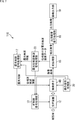
図1は、本技術を適用した撮像装置の第1の実施の形態の構成例を示すブロック図である。
図1において、撮像装置11は、光学装置12、AF制御信号処理部13、撮像素子14、前処理部15、露光検波信号処理部16、露光制御信号処理部17、出力画像信号処理部18、画像出力部19、および操作信号処理部20を備えて構成される。
光学装置12は、複数枚の光学レンズやAF駆動部などを有しており、光学レンズにより被写体からの光を集光し、AF制御信号処理部13による制御に従って光学レンズを駆動することで、撮像素子14のセンサ面に被写体の像を結像させる。
AF制御信号処理部13は、例えば、図示しないラインセンサの出力や撮像画像のコントラストなどに基づいて、または、後述する図7の露光位相差検波信号処理装置22からの位相差検波情報に基づいて、被写体にピントが合うように、光学装置12のAF駆動部を制御する。
撮像素子14は、複数の画素が行列状に配置されたセンサ面を有しており、画像の撮像に利用される撮像有効領域に配置された画素の受光量に応じた画素値により構築される撮像画像を前処理部15に供給する。また、撮像素子14のセンサ面には、通常の撮像に使用される画素の他に、撮像環境の明るさを検出することに特化した画素(以下、OPD(Optical Photo Detector)画素と称する)が配置されている。
また、撮像素子14のOPD画素には、ダイナミックレンジを広く取ることができる構成が採用される。例えば、OPD画素としては、光量に対して対数的な画素信号を出力し、強い光を受光しても飽和しない対数画素を用いることができる。また、HDR(High Dynamic Range)画像の撮像と同様に、感度または露光時間の異なる複数の画素を1つのOPD画素として用いることができる。なお、以下適宜、撮像素子14のセンサ面に配置されている画素のうち、OPD画素以外の画素を有効画素と称し、画像の構築に有効に用いられる有効画素よりも、OPD画素の画素値が高ダイナミックレンジ(より広範囲の光量を識別可能)とされる。
前処理部15は、撮像素子14から供給される撮像画像から、OPD画素により得られる画素値を抽出し、露光検波画素データとして露光検波信号処理部16に供給する。また、前処理部15は、撮像素子14から供給される撮像画像のうち、有効画素により得られる画素値を用いて、OPD画素の配置位置に対応する箇所の画素値を補間して求める補正処理を行う。
ここで、例えば、撮像素子14では、ベイヤ配列に従って、赤色、緑色、青色のカラーフィルタが有効画素に配置されており、OPD画素では、明るさを検出するために無色とされている。従って、前処理部15は、ベイヤ配列に従って、OPD画素の配置箇所に本来配置されていた色と同色であって、かつ、そのOPD画素の近隣にある複数の有効画素の画素値を線形補間することにより、OPD画素の配置位置に対応する箇所の画素値を求める。そして、前処理部15は、撮像画像に補正処理を施すことにより得られる補正画像を出力画像信号処理部18に供給する。
露光検波信号処理部16は、前処理部15から供給される露光検波画素データに対して、例えば、空間方向に積分することによって検波を行い、被写体の露光状態を検出した露光検波情報を取得し、露光制御信号処理部17に供給する。
露光制御信号処理部17は、露光検波信号処理部16から供給される露光検波情報に基づいて、被写体が適切な明るさで撮像されるような撮像素子14の露光時間を求め、撮像素子14に対する露光制御を行う。
出力画像信号処理部18は、前処理部15から供給される補正画像に対して、例えば、ホワイトバランス調整やガンマ補正などの各種の画像処理を施す。そして、出力画像信号処理部18は、補正画像に画像処理を施すことにより得られる出力画像を画像出力部19に供給する。
画像出力部19は、例えば、液晶パネルや有機EL(Electro Luminescence)パネルなどの表示デバイスを有しており、出力画像信号処理部18から供給される出力画像を表示する。また、画像出力部19は、内蔵型または着脱可能な記録媒体により構成され、出力画像信号処理部18から供給される出力画像を記録する。
操作信号処理部20は、図示しない操作部に対してユーザが行った操作に応じた操作信号が供給され、その操作信号に基づいた処理を行う。例えば、操作信号処理部20は、撮像装置11の撮像モードを静止画像または動画像に設定する操作に応じて、静止画像または動画像を撮像するように撮像素子14に対する制御を行う。また、例えば、操作信号処理部20は、撮像装置11の撮像モードが静止画像であるときに、シャッタ操作が行われると、その操作が行われたタイミングの静止画像を出力するように撮像素子14に対する制御を行う。また、操作信号処理部20は、ユーザの操作に従って、AF制御信号処理部13および露光制御信号処理部17において行われる処理に対する各種の設定を行う。
このように構成される撮像装置11は、OPD画素により被写体の露光状態を常に観測することができ、常に適切な露光制御を行うことができる。
また、例えば、従来の撮像装置において撮像画像から露光状態を測定してAE制御を行う構成では、特にコントラストの高い被写体で白とび(オーバー露出)および黒潰れ(アンダー露出)などによる情報の損失が発生し、AE制御の収束に時間を要することになっていた。
これに対し、撮像装置11では、ダイナミックレンジの広いOPD画素の画素値に基づいてAE制御を行うことができるため、コントラストの高い被写体であっても画素値が飽和することなく、迅速に(1フレームで)最適な露光状態に調整することができる。即ち、撮像装置11では、どのような露光状態からでも高速に適正露出となるように制御することができる。
次に、図2を参照して、撮像素子14のセンサ面に配置されるOPD画素の第1の配置例について説明する。
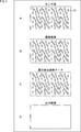
図2のAには、撮像素子14のセンサ面が示されており、図示するように、OPD画素31は、センサ面においてランダムに配置することができる。
このようにOPD画素31がランダムに配置された構成の撮像素子14により撮像された撮像画像は、図2のBに示すように、OPD画素31の配置位置に従ってランダムに、OPD画素の画素値が配置されたものとなる。そして、前処理部15は、このような撮像画像からOPD画素の画素値を抽出することで、図2のCに示すような露光検波画素データを取得する。このような露光検波画素データを用いて、露光検波信号処理部16により検波が行われ、露光制御信号処理部17により露光制御が行われる。
一方、前処理部15は、撮像画像から露光検波画素データを抽出した残りの画素値を用いて、即ち、有効画素の画素値を用いて、OPD画素の配置位置に対応する箇所の画素値を補間する補正処理を行う。これにより、前処理部15は、撮像素子14の全ての画素位置における画素値から構成される補正画像を出力し、出力画像信号処理部18により画像処理が施されて、図2のDに示すような出力画像が出力される。
このように、OPD画素31がランダムに配置された撮像素子14は、例えば、周期的な模様を有する被写体に対しても、その周期性に影響を受けることなく、正確に露光制御を行うことができる。
次に、図3を参照して、撮像素子14のセンサ面に配置されるOPD画素の第2の配置例について説明する。
図3のAには、撮像素子14のセンサ面が示されており、図示するように、OPD画素31は、センサ面において水平方向に沿って複数本のライン状に配置することができる。
このようにOPD画素31がライン状に配置された構成の撮像素子14により撮像された撮像画像は、図3のBに示すように、OPD画素31の配置に従ってライン状に、OPD画素の画素値が配置されたものとなる。そして、前処理部15は、このような撮像画像からOPD画素の画素値を抽出することで、図3のCに示すような露光検波画素データを取得する。このような露光検波画素データを用いて、露光検波信号処理部16により検波が行われ、露光制御信号処理部17により露光制御が行われる。
一方、前処理部15は、撮像画像から露光検波画素データを抽出した残りの画素値を用いて、即ち、有効画素の画素値を用いて、OPD画素の配置位置に対応する箇所の画素値を補間する補正処理を行う。これにより、前処理部15は、撮像素子14の全ての画素位置における画素値から構成される補正画像を出力し、出力画像信号処理部18により画像処理が施されて、図3のDに示すような出力画像が出力される。
このように、OPD画素31がライン状に配置された撮像素子14は、例えば、1列ごとに駆動を行うため、簡易的な駆動制御によって撮像画像を出力することができる。また、図2に示したようなランダムな配置と比較して、ライン状の配置は、構造的に容易に製造することができる。
なお、OPD画素31の配置方法については、上述したようなランダムまたはライン的な配置に限定されることなく、それら以外の様々な配置を採用することができる。
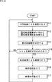
次に、図4のフローチャートを参照して、撮像装置11により静止画像を撮像する処理について説明する。
例えば、ユーザが、図示しない操作部を操作して、撮像装置11の撮像モードを静止画像に設定すると処理が開始される。ステップS11において、操作信号処理部20は、ユーザの操作に従って、OPD画素31の画素値のみを読み出すように撮像素子14に対する制御を行い、撮像素子14は、OPD画素31のみを駆動し、OPD画素31による撮像を行う。これにより、OPD画素31の画素値のみで構成される撮像画像が撮像素子14から前処理部15に供給される。
ステップS12において、前処理部15は、ステップS11で撮像素子14から供給されたOPD画素31の画素値のみで構成される撮像画像を、露光検波画素データとして露光検波信号処理部16に供給する。露光検波信号処理部16は、露光検波画素データから露光検波情報を取得して、露光制御信号処理部17に供給する。
ステップS13において、露光制御信号処理部17は、ステップS12で露光検波信号処理部16から供給された露光検波情報に基づいて、被写体を最適な明るさで撮像することができる撮像素子14の露光時間を求め、撮像素子14に対する制御を行うための露光制御値を決定する。そして、露光制御信号処理部17は、その露光制御値に従って撮像素子14に対する露光時間の制御を行う。
ステップS14において、操作信号処理部20は、ユーザによりシャッタ操作が行われたか否かを判定する。例えば、ユーザが、図示しないシャッタボタンに対する操作を行い、その操作信号が操作信号処理部20に供給されると、操作信号処理部20は、ユーザによりシャッタ操作が行われたと判定する。
ステップS14において、操作信号処理部20が、ユーザによりシャッタ操作が行われていないと判定した場合、処理はステップS11に戻り、以下、同様の処理が繰り返される。一方、ステップS14において、操作信号処理部20が、ユーザによりシャッタ操作が行われたと判定した場合、処理はステップS15に進む。
ステップS15において、操作信号処理部20は、有効画素の画素値を読み出すように撮像素子14に対する制御を行い、撮像素子14は有効画素を駆動して、有効画素による撮像を行う。このとき、撮像素子14は、直前のステップS13で決定された露光制御値に従った露光時間で、有効画素による撮像を行うことになる。
ステップS16において、前処理部15は、ステップS18で撮像素子14から供給された有効画素の画素値で構成される撮像画像を用いて、OPD画素の配置位置に対応する箇所の画素値を補間する補正処理を行い、補正画像を出力画像信号処理部18に供給する。
ステップS17において、出力画像信号処理部18は、ステップS16で前処理部15から供給された補正画像に対して画像処理を施した出力画像を、画像出力部19に供給して表示または記録させる。ステップS17の処理後、処理はステップS11に戻り、以下、同様の処理が繰り返される。
以上のように、撮像装置11で静止画像を撮像する場合、ユーザによりシャッタ操作が行われるまで待機する待機時において、撮像素子14のOPD画素31の画素値のみを読み出すような駆動を行うことができ、低電力化を図ることができる。
即ち、従来の撮像素子では、待機時においても撮像素子の全ての画素から画素値の読み出しが行われていた。これに対し、撮像装置11では、撮像素子14のOPD画素31の画素値のみを読み出すことにより、OPD画素31が、撮像素子14の全画素に対する5%の割合で埋め込まれる構成では、待機時において、駆動電力の約95%を削減することができる。さらに、撮像装置11では、待機時において、露光検波信号処理部16および露光制御信号処理部17を駆動させる一方、出力画像信号処理部18の処理を停止させることができるため、さらなる駆動電力の削減を見込むことができる。
次に、図5のフローチャートを参照して、撮像装置11により動画像を撮像する処理について説明する。
例えば、ユーザが、図示しない操作部を操作して、撮像装置11の撮像モードを動画像に設定すると処理が開始される。ステップS21において、操作信号処理部20は、ユーザの操作に従って、OPD画素31および有効画素の画素値を読み出すように撮像素子14に対する制御を行い、撮像素子14は、OPD画素31および有効画素による撮像を行う。これにより、OPD画素31および有効画素の画素値で構成される撮像画像が撮像素子14から前処理部15に供給される。
ステップS22において、前処理部15は、ステップS11で撮像素子14から供給されたOPD画素31および有効画素の画素値で構成される撮像画像から、OPD画素31の画素値を抽出し、露光検波画素データとして露光検波信号処理部16に供給する。
ステップS23において、露光検波信号処理部16は、ステップS22で前処理部15から供給される露光検波画素データから露光検波情報を取得して、露光制御信号処理部17に供給する。
ステップS24において、露光制御信号処理部17は、ステップS22で露光検波信号処理部16から供給された露光検波情報に基づいて、被写体を最適な明るさで撮像することができる撮像素子14の露光時間を求め、撮像素子14に対する制御を行うための露光制御値を決定する。そして、露光制御信号処理部17は、その露光制御値に従って撮像素子14に対する露光時間の制御を行う。これにより、次の1フレームの撮像画像を撮像素子14により撮像する際に、直前のステップS24で露光制御信号処理部17が決定した露光制御値に従った露光時間で撮像が行われる。
ステップS25において、前処理部15は、OPD画素31および有効画素の画素値で構成される撮像画像から、OPD画素31の画素値が抽出された残りの画素値(即ち、有効画素の画素値のみ)から構成される撮像画像を用いて、OPD画素の配置位置に対応する箇所の画素値を補間する補正処理を行い、補正画像を出力画像信号処理部18に供給する。
ステップS26において、出力画像信号処理部18は、ステップS25で前処理部15から供給された補正画像に対して画像処理を施した出力画像を、画像出力部19に供給して表示または記録させる。ステップS26の処理後、処理はステップS21に戻り、以下、同様の処理が繰り返される。
以上のように、撮像装置11で動画像を撮像する場合、撮像素子14は、1フレーム前の撮像画像に基づいて決定された露光制御値に従って撮像を行うことができる。従って、撮像装置11は、被写体の露光環境が急激に変化するような状況であっても、常に、迅速に(1フレームで)最適な露光に収束することができ、より高い即応性を備えることができる。
<撮像装置の第2の実施の形態>
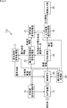
次に、図6は、本技術を適用した撮像装置の第2の実施の形態の構成例を示すブロック図である。
図6に示すように、撮像装置11Aは、光学装置12、AF制御信号処理部13、撮像素子14A、前処理部15、露光検波信号処理部16、露光制御信号処理部17、出力画像信号処理部18、画像出力部19、操作信号処理部20、およびAWB制御信号処理装置21を備えて構成される。ここで、撮像装置11Aにおいて、図1の撮像装置11と共通の構成となるブロックについては、同一の符号を付し、その詳細な説明は省略する。
即ち、撮像装置11Aは、撮像素子14AおよびAWB制御信号処理装置21を備える点で、図1の撮像装置11と異なる構成となっている。
撮像素子14Aは、図1の撮像素子14と同様に、OPD画素がランダムまたはライン状に配置されている。そして、図1の撮像素子14のOPD画素は、明るさのみを検出することができるのに対し、撮像素子14AのOPD画素は、色情報を有する明るさを検出することができる。つまり、撮像素子14Aは、所定の色(例えば、赤色、青色、緑色、または赤外の波長域)の光を透過するカラーフィルタがOPD画素に積層されて構成され、それぞれの色ごとの明るさを、OPD画素の画素値とした撮像画像を出力することができる。
前処理部15は、撮像素子14から供給される撮像画像から、OPD画素の画素値を抽出し、色別検波画素データとして露光検波信号処理部16に供給する。
露光検波信号処理部16は、前処理部15から供給される色別検波画素データに対して色ごとに検波を行い、色検波情報をAWB制御信号処理装置21に供給する。また、露光検波信号処理部16は、色ごとのバランスを取った割合(例えば、赤色:青色:緑色=6:3:1)で色別検波画素データに対する検波を行って得られる露光検波情報を露光制御信号処理部17に供給する。
AWB制御信号処理装置21は、露光検波信号処理部16から供給される色検波情報に基づいて、被写体の色味が正確に再現されるようなホワイトバランスを求め、出力画像信号処理部18に対するホワイトバランス制御を行う。
出力画像信号処理部18は、AWB制御信号処理装置21の制御に従い、前処理部15から供給される補正画像に対してホワイトバランスを調整する画像処理を行って、出力画像を画像出力部19に供給する。
このように構成される撮像装置11Aでは、OPD画素の画素値に基づいて露光制御を行うのに加えて、AWB制御も同時に実現することができる。なお、撮像装置11Aでは、カラーフィルタが積層されているOPD画素の画素値が色情報を有することより、前処理部15が、所定のOPD画素の画素値を周辺の有効画素の画素値から補間する補正処理を行う際に、そのOPD画素自身の画素値も使用することができる。
<撮像装置の第3の実施の形態>
次に、図7は、本技術を適用した撮像装置の第3の実施の形態の構成例を示すブロック図である。
図7に示すように、撮像装置11Bは、光学装置12、AF制御信号処理部13、撮像素子14B、前処理部15、露光制御信号処理部17、出力画像信号処理部18、画像出力部19、操作信号処理部20、および露光位相差検波信号処理装置22を備えて構成される。ここで、撮像装置11Bにおいて、図1の撮像装置11と共通の構成となるブロックについては、同一の符号を付し、その詳細な説明は省略する。
即ち、撮像装置11Bは、撮像素子14Bおよび露光位相差検波信号処理装置22を備える点で、図1の撮像装置11と異なる構成となっている。
撮像素子14Bでは、OPD画素が、撮像面における位相差を検出するように、被写体からの光を受光する受光部が分割されて構成されている。従って、OPD画素から出力される画素値は、分割された受光部それぞれの受光量に応じたものとなり、それらの受光部からの出力差に基づいて、撮像素子14Bの像面における位相差が求められる。
このようなOPD画素から出力される画素値が、位相差付き露光検波画素データとして露光位相差検波信号処理装置22に供給される。そして、露光位相差検波信号処理装置22は、OPD画素の受光部それぞれの画素値の差分に基づいて、撮像素子14Bの像面における位相差を求め、AF制御信号処理部13に対して位相差検波情報を供給する。
これにより、AF制御信号処理部13は、位相差検波情報に基づいて、撮像素子14Bに対するAF制御を行うことができる。
このように構成される撮像装置11Bでは、OPD画素の画素値に基づいて露光制御を行うのに加えて、AF制御も同時に実現することができる。
<撮像装置の第4の実施の形態>
次に、図8は、本技術を適用した撮像装置の第4の実施の形態の構成例を示すブロック図である。
図8に示すように、撮像装置11Cは、光学装置12、AF制御信号処理部13、撮像素子14C、前処理部15、露光制御信号処理部17、出力画像信号処理部18、画像出力部19、操作信号処理部20、AWB制御信号処理装置21、および露光位相差検波信号処理装置22を備えて構成される。ここで、撮像装置11Cにおいて、図1の撮像装置11と共通の構成となるブロックについては、同一の符号を付し、その詳細な説明は省略する。
即ち、撮像装置11Cは、図6のAWB制御信号処理装置21および図7の露光位相差検波信号処理装置22を備えて構成される。また、撮像装置11Cの撮像素子14Cは、図6の撮像素子14Aと同様に、赤色、青色、または緑色のカラーフィルタがOPD画素に積層されて構成されるとともに、図7の撮像素子14Bと同様に、像面位相差検出を行うことができるように構成されている。
つまり、撮像装置11Cは、図6の撮像装置11Aおよび図7の撮像装置11Bの両方の機能を備えて構成され、上述したようなAE制御、AWB制御、およびAF制御を全て同時に実現することができる。
なお、本実施の形態の撮像装置11において、拡張ダイナミックレンジ撮像のような特殊な露光形態を実装する際に、OPD画素の画素値が飽和しないという特性を利用して、各露光状態を適切に制御することができる。これにより、撮像装置11では、拡張ダイナミックレンジ撮像における視認性および階調感を最適にする調整を容易に行うことができる。
また、撮像装置11におけるAE制御、AWB制御、およびAF制御は、ファームウェアなどの制御機構により実現することができ、撮像素子14の特性に応じた制御を容易に実現することができる。
<イメージセンサの使用例>
図9は、イメージセンサ(撮像装置11が備える撮像素子14)を使用する使用例を示す図である。
上述したイメージセンサは、例えば、以下のように、可視光や、赤外光、紫外光、X線等の光をセンシングする様々なケースに使用することができる。
・ディジタルカメラや、カメラ機能付きの携帯機器等の、鑑賞の用に供される画像を撮影する装置
・自動停止等の安全運転や、運転者の状態の認識等のために、自動車の前方や後方、周囲、車内等を撮影する車載用センサ、走行車両や道路を監視する監視カメラ、車両間等の測距を行う測距センサ等の、交通の用に供される装置
・ユーザのジェスチャを撮影して、そのジェスチャに従った機器操作を行うために、TVや、冷蔵庫、エアーコンディショナ等の家電に供される装置
・内視鏡や、赤外光の受光による血管撮影を行う装置等の、医療やヘルスケアの用に供される装置
・防犯用途の監視カメラや、人物認証用途のカメラ等の、セキュリティの用に供される装置
・肌を撮影する肌測定器や、頭皮を撮影するマイクロスコープ等の、美容の用に供される装置
・スポーツ用途等向けのアクションカメラやウェアラブルカメラ等の、スポーツの用に供される装置
・畑や作物の状態を監視するためのカメラ等の、農業の用に供される装置
・自動停止等の安全運転や、運転者の状態の認識等のために、自動車の前方や後方、周囲、車内等を撮影する車載用センサ、走行車両や道路を監視する監視カメラ、車両間等の測距を行う測距センサ等の、交通の用に供される装置
・ユーザのジェスチャを撮影して、そのジェスチャに従った機器操作を行うために、TVや、冷蔵庫、エアーコンディショナ等の家電に供される装置
・内視鏡や、赤外光の受光による血管撮影を行う装置等の、医療やヘルスケアの用に供される装置
・防犯用途の監視カメラや、人物認証用途のカメラ等の、セキュリティの用に供される装置
・肌を撮影する肌測定器や、頭皮を撮影するマイクロスコープ等の、美容の用に供される装置
・スポーツ用途等向けのアクションカメラやウェアラブルカメラ等の、スポーツの用に供される装置
・畑や作物の状態を監視するためのカメラ等の、農業の用に供される装置
なお、本技術は以下のような構成も取ることができる。
(1)
被写体の明るさの検出に用いられる画素値を出力する露光検出画素、および、画像の構築に有効な画素値を出力する有効画素が、前記画像の撮像に利用される撮像有効領域に配置された撮像素子と、
前記露光検出画素から出力される画素値に基づいて、前記撮像素子の露光を制御する露光制御部と
を備え、
前記露光検出画素の画素値が、前記有効画素の画素値よりも高ダイナミックレンジである
撮像装置。
(2)
前記撮像素子に前記露光検出画素が配置されている箇所において前記画像を構築するための画素値を、前記露光検出画素の近傍にある前記有効画素の画素値から補間して求める補正処理を行う補正処理部
をさらに備える上記(1)に記載の撮像装置。
(3)
前記撮像素子は、静止画像を撮像する撮像モードであるとき、静止画像の撮像を指示するシャッタ操作が行われるまで待機する待機時において、前記露光検出画素のみから画素値の読み出しを行う
上記(1)または(2)に記載の撮像装置。
(4)
前記撮像素子は、動画像を撮像する撮像モードであるとき、1フレーム前の前記露光検出画素の画素値に基づいた露光で撮像を行う
上記(1)から(3)までのいずれかに記載の撮像装置。
(5)
前記撮像素子は、所定の波長域の光を透過するカラーフィルタを前記露光検出画素に積層して構成されており、
前記波長域ごとの前記露光検出画素の画素値を検波して得られる色検波情報を出力する色別検波部と、
前記色検波情報に基づいて、前記補正処理部により前記補正処理が施された画像に対するホワイトバランスを調整する画像処理を行う画像処理部と
をさらに備える上記(2)から(4)までのいずれかに記載の撮像装置。
(6)
前記補正処理部は、前記補正処理を行う際に、前記カラーフィルタが積層されている前記露光検出画素自身の画素値も使用する
上記(5)に記載の撮像装置。
(7)
前記露光検出画素は、前記露光検出画素および前記有効画素が配置される前記撮像素子の撮像面における位相差を検出するように、被写体からの光を受光する受光部が分割されて構成されており、
前記露光検出画素の分割された前記受光部からの出力差に基づいて、前記撮像素子の撮像面における位相差を検出する像面位相差検出部と、
前記撮像素子の撮像面における位相差に従って、前記被写体の像を前記撮像素子に結像する光学系を駆動して焦点制御を行う焦点制御部と
をさらに備える
上記(1)から(6)までのいずれかに記載の撮像装置。
(8)
被写体の明るさの検出に用いられる画素値を出力する露光検出画素、および、画像の構築に有効な画素値を出力する有効画素が、前記画像の撮像に利用される撮像有効領域に配置され、前記露光検出画素の画素値が、前記有効画素の画素値よりも高ダイナミックレンジである撮像素子を備える撮像装置の撮像方法であって、
前記露光検出画素から出力される画素値に基づいて、前記撮像素子の露光を制御するステップを含む
撮像方法。
(1)
被写体の明るさの検出に用いられる画素値を出力する露光検出画素、および、画像の構築に有効な画素値を出力する有効画素が、前記画像の撮像に利用される撮像有効領域に配置された撮像素子と、
前記露光検出画素から出力される画素値に基づいて、前記撮像素子の露光を制御する露光制御部と
を備え、
前記露光検出画素の画素値が、前記有効画素の画素値よりも高ダイナミックレンジである
撮像装置。
(2)
前記撮像素子に前記露光検出画素が配置されている箇所において前記画像を構築するための画素値を、前記露光検出画素の近傍にある前記有効画素の画素値から補間して求める補正処理を行う補正処理部
をさらに備える上記(1)に記載の撮像装置。
(3)
前記撮像素子は、静止画像を撮像する撮像モードであるとき、静止画像の撮像を指示するシャッタ操作が行われるまで待機する待機時において、前記露光検出画素のみから画素値の読み出しを行う
上記(1)または(2)に記載の撮像装置。
(4)
前記撮像素子は、動画像を撮像する撮像モードであるとき、1フレーム前の前記露光検出画素の画素値に基づいた露光で撮像を行う
上記(1)から(3)までのいずれかに記載の撮像装置。
(5)
前記撮像素子は、所定の波長域の光を透過するカラーフィルタを前記露光検出画素に積層して構成されており、
前記波長域ごとの前記露光検出画素の画素値を検波して得られる色検波情報を出力する色別検波部と、
前記色検波情報に基づいて、前記補正処理部により前記補正処理が施された画像に対するホワイトバランスを調整する画像処理を行う画像処理部と
をさらに備える上記(2)から(4)までのいずれかに記載の撮像装置。
(6)
前記補正処理部は、前記補正処理を行う際に、前記カラーフィルタが積層されている前記露光検出画素自身の画素値も使用する
上記(5)に記載の撮像装置。
(7)
前記露光検出画素は、前記露光検出画素および前記有効画素が配置される前記撮像素子の撮像面における位相差を検出するように、被写体からの光を受光する受光部が分割されて構成されており、
前記露光検出画素の分割された前記受光部からの出力差に基づいて、前記撮像素子の撮像面における位相差を検出する像面位相差検出部と、
前記撮像素子の撮像面における位相差に従って、前記被写体の像を前記撮像素子に結像する光学系を駆動して焦点制御を行う焦点制御部と
をさらに備える
上記(1)から(6)までのいずれかに記載の撮像装置。
(8)
被写体の明るさの検出に用いられる画素値を出力する露光検出画素、および、画像の構築に有効な画素値を出力する有効画素が、前記画像の撮像に利用される撮像有効領域に配置され、前記露光検出画素の画素値が、前記有効画素の画素値よりも高ダイナミックレンジである撮像素子を備える撮像装置の撮像方法であって、
前記露光検出画素から出力される画素値に基づいて、前記撮像素子の露光を制御するステップを含む
撮像方法。
なお、本実施の形態は、上述した実施の形態に限定されるものではなく、本開示の要旨を逸脱しない範囲において種々の変更が可能である。
11 撮像装置, 12 光学装置, 13 AF制御信号処理部, 14 撮像素子, 15 前処理部, 16 露光検波信号処理部, 17 露光制御信号処理部, 18 出力画像信号処理部, 19 画像出力部, 20 操作信号処理部, 21 AWB制御信号処理装置, 22 露光位相差検波信号処理装置, 31 OPD画素31
Claims (8)
- 被写体の明るさの検出に用いられる画素値を出力する露光検出画素、および、画像の構築に有効な画素値を出力する有効画素が、前記画像の撮像に利用される撮像有効領域に配置された撮像素子と、
前記露光検出画素から出力される画素値に基づいて、前記撮像素子の露光を制御する露光制御部と
を備え、
前記露光検出画素の画素値が、前記有効画素の画素値よりも高ダイナミックレンジである
撮像装置。 - 前記撮像素子に前記露光検出画素が配置されている箇所において前記画像を構築するための画素値を、前記露光検出画素の近傍にある前記有効画素の画素値から補間して求める補正処理を行う補正処理部
をさらに備える請求項1に記載の撮像装置。 - 前記撮像素子は、静止画像を撮像する撮像モードであるとき、静止画像の撮像を指示するシャッタ操作が行われるまで待機する待機時において、前記露光検出画素のみから画素値の読み出しを行う
請求項1に記載の撮像装置。 - 前記撮像素子は、動画像を撮像する撮像モードであるとき、1フレーム前の前記露光検出画素の画素値に基づいた露光で撮像を行う
請求項1に記載の撮像装置。 - 前記撮像素子は、所定の波長域の光を透過するカラーフィルタを前記露光検出画素に積層して構成されており、
前記波長域ごとの前記露光検出画素の画素値を検波して得られる色検波情報を出力する色別検波部と、
前記色検波情報に基づいて、前記補正処理部により前記補正処理が施された画像に対するホワイトバランスを調整する画像処理を行う画像処理部と
をさらに備える請求項2に記載の撮像装置。 - 前記補正処理部は、前記補正処理を行う際に、前記カラーフィルタが積層されている前記露光検出画素自身の画素値も使用する
請求項5に記載の撮像装置。 - 前記露光検出画素は、前記露光検出画素および前記有効画素が配置される前記撮像素子の撮像面における位相差を検出するように、被写体からの光を受光する受光部が分割されて構成されており、
前記露光検出画素の分割された前記受光部からの出力差に基づいて、前記撮像素子の撮像面における位相差を検出する像面位相差検出部と、
前記撮像素子の撮像面における位相差に従って、前記被写体の像を前記撮像素子に結像する光学系を駆動して焦点制御を行う焦点制御部と
をさらに備える請求項1に記載の撮像装置。 - 被写体の明るさの検出に用いられる画素値を出力する露光検出画素、および、画像の構築に有効な画素値を出力する有効画素が、前記画像の撮像に利用される撮像有効領域に配置され、前記露光検出画素の画素値が、前記有効画素の画素値よりも高ダイナミックレンジである撮像素子を備える撮像装置の撮像方法であって、
前記露光検出画素から出力される画素値に基づいて、前記撮像素子の露光を制御するステップを含む
撮像方法。
Priority Applications (1)
| Application Number | Priority Date | Filing Date | Title |
|---|---|---|---|
| US15/737,083 US20180176445A1 (en) | 2015-06-23 | 2016-06-09 | Imaging device and imaging method |
Applications Claiming Priority (2)
| Application Number | Priority Date | Filing Date | Title |
|---|---|---|---|
| JP2015-125360 | 2015-06-23 | ||
| JP2015125360A JP2017011513A (ja) | 2015-06-23 | 2015-06-23 | 撮像装置および撮像方法 |
Publications (1)
| Publication Number | Publication Date |
|---|---|
| WO2016208405A1 true WO2016208405A1 (ja) | 2016-12-29 |
Family
ID=57585632
Family Applications (1)
| Application Number | Title | Priority Date | Filing Date |
|---|---|---|---|
| PCT/JP2016/067194 Ceased WO2016208405A1 (ja) | 2015-06-23 | 2016-06-09 | 撮像装置および撮像方法 |
Country Status (3)
| Country | Link |
|---|---|
| US (1) | US20180176445A1 (ja) |
| JP (1) | JP2017011513A (ja) |
| WO (1) | WO2016208405A1 (ja) |
Cited By (2)
| Publication number | Priority date | Publication date | Assignee | Title |
|---|---|---|---|---|
| CN109104584A (zh) * | 2017-06-21 | 2018-12-28 | 比亚迪股份有限公司 | 图像传感器及其高动态范围图像的获取方法 |
| CN111201778A (zh) * | 2017-10-19 | 2020-05-26 | 索尼公司 | 成像装置、曝光控制方法、程序和成像器件 |
Families Citing this family (2)
| Publication number | Priority date | Publication date | Assignee | Title |
|---|---|---|---|---|
| EP4209001B1 (en) | 2020-09-04 | 2025-06-25 | QUALCOMM Incorporated | Sensitivity-biased pixels |
| JP2024092602A (ja) * | 2022-12-26 | 2024-07-08 | ソニーセミコンダクタソリューションズ株式会社 | 光検出素子及び電子機器 |
Citations (3)
| Publication number | Priority date | Publication date | Assignee | Title |
|---|---|---|---|---|
| JP2000156823A (ja) * | 1998-08-20 | 2000-06-06 | Canon Inc | 固体撮像装置及びその制御方法及び撮像装置及び光電変換セルの基本配列及び記憶媒体 |
| JP2002290824A (ja) * | 2001-03-27 | 2002-10-04 | Minolta Co Ltd | デジタルカメラ |
| JP2011059337A (ja) * | 2009-09-09 | 2011-03-24 | Fujifilm Corp | 撮像装置 |
Family Cites Families (8)
| Publication number | Priority date | Publication date | Assignee | Title |
|---|---|---|---|---|
| US7088395B2 (en) * | 2001-01-29 | 2006-08-08 | Konica Corporation | Image-capturing apparatus |
| KR101086403B1 (ko) * | 2004-09-10 | 2011-11-25 | 삼성전자주식회사 | 디지털 촬영 장치의 제어 방법 및 이 방법을 채용한디지털 촬영 장치 |
| JP2008306439A (ja) * | 2007-06-07 | 2008-12-18 | Konica Minolta Holdings Inc | 撮像素子および撮像装置 |
| US8253812B2 (en) * | 2008-02-23 | 2012-08-28 | Sanyo Electric Co., Ltd. | Video camera which adopts a focal-plane electronic shutter system |
| JP5422362B2 (ja) * | 2009-12-15 | 2014-02-19 | 株式会社東芝 | 固体撮像装置 |
| JP2013066142A (ja) * | 2011-08-31 | 2013-04-11 | Sony Corp | 画像処理装置、および画像処理方法、並びにプログラム |
| JP5542247B2 (ja) * | 2012-03-30 | 2014-07-09 | 富士フイルム株式会社 | 撮像素子及び撮像装置 |
| US9509919B2 (en) * | 2014-11-17 | 2016-11-29 | Duelight Llc | System and method for generating a digital image |
-
2015
- 2015-06-23 JP JP2015125360A patent/JP2017011513A/ja active Pending
-
2016
- 2016-06-09 WO PCT/JP2016/067194 patent/WO2016208405A1/ja not_active Ceased
- 2016-06-09 US US15/737,083 patent/US20180176445A1/en not_active Abandoned
Patent Citations (3)
| Publication number | Priority date | Publication date | Assignee | Title |
|---|---|---|---|---|
| JP2000156823A (ja) * | 1998-08-20 | 2000-06-06 | Canon Inc | 固体撮像装置及びその制御方法及び撮像装置及び光電変換セルの基本配列及び記憶媒体 |
| JP2002290824A (ja) * | 2001-03-27 | 2002-10-04 | Minolta Co Ltd | デジタルカメラ |
| JP2011059337A (ja) * | 2009-09-09 | 2011-03-24 | Fujifilm Corp | 撮像装置 |
Cited By (5)
| Publication number | Priority date | Publication date | Assignee | Title |
|---|---|---|---|---|
| CN109104584A (zh) * | 2017-06-21 | 2018-12-28 | 比亚迪股份有限公司 | 图像传感器及其高动态范围图像的获取方法 |
| CN111201778A (zh) * | 2017-10-19 | 2020-05-26 | 索尼公司 | 成像装置、曝光控制方法、程序和成像器件 |
| EP3700191A4 (en) * | 2017-10-19 | 2020-08-26 | Sony Corporation | IMAGING DEVICE, EXPOSURE CONTROL PROCESS, PROGRAM, AND IMAGING ELEMENT |
| CN111201778B (zh) * | 2017-10-19 | 2022-02-08 | 索尼公司 | 成像装置、曝光控制方法、计算机可读存储介质和成像器件 |
| US11451715B2 (en) | 2017-10-19 | 2022-09-20 | Sony Corporation | Imaging apparatus, exposure controlling method, and imaging device |
Also Published As
| Publication number | Publication date |
|---|---|
| JP2017011513A (ja) | 2017-01-12 |
| US20180176445A1 (en) | 2018-06-21 |
Similar Documents
| Publication | Publication Date | Title |
|---|---|---|
| JP5331945B2 (ja) | 撮像装置及びその駆動方法 | |
| JP5736796B2 (ja) | 電子カメラ、プログラム及び記録媒体 | |
| CN103685876B (zh) | 摄像装置、摄像方法以及记录介质 | |
| WO2017037978A1 (ja) | 検出装置、検出方法、検出プログラムおよび撮像装置 | |
| TWI492618B (zh) | 攝影裝置及電腦可讀取記錄媒體 | |
| US20190243533A1 (en) | Display controller, control method thereof, and non-transitory computer readable medium | |
| JP5302058B2 (ja) | 撮像装置および撮像方法 | |
| JP2014235224A (ja) | 撮像装置および制御プログラム | |
| JP2017011513A (ja) | 撮像装置および撮像方法 | |
| JP5146015B2 (ja) | 撮像装置及び撮像方法 | |
| JP4649550B2 (ja) | カメラ | |
| JP6482247B2 (ja) | 焦点調節装置、撮像装置、焦点調節装置の制御方法、及びプログラム | |
| JP2011055251A5 (ja) | 撮像制御装置および方法 | |
| JP6257316B2 (ja) | 撮像装置およびその制御方法 | |
| WO2019065820A1 (ja) | 撮影装置とその制御方法および制御プログラム | |
| JP2011018989A (ja) | 撮像装置、画像選択方法、及び、プログラム | |
| JP5470218B2 (ja) | 撮像装置 | |
| JP2010134291A (ja) | 撮像装置及びその制御方法 | |
| JP4871664B2 (ja) | 撮像装置及び撮像装置の制御方法 | |
| JP2006253887A (ja) | 撮像装置 | |
| JP2008283477A (ja) | 画像処理装置及び画像処理方法 | |
| JP2007116372A (ja) | デジタルカメラ | |
| JP5938269B2 (ja) | 撮像装置およびその制御方法 | |
| JP5672922B2 (ja) | 撮像装置 | |
| JP6479149B2 (ja) | 撮像装置、撮像装置の制御方法、および画像処理装置 |
Legal Events
| Date | Code | Title | Description |
|---|---|---|---|
| 121 | Ep: the epo has been informed by wipo that ep was designated in this application |
Ref document number: 16814176 Country of ref document: EP Kind code of ref document: A1 |
|
| WWE | Wipo information: entry into national phase |
Ref document number: 15737083 Country of ref document: US |
|
| NENP | Non-entry into the national phase |
Ref country code: DE |
|
| 122 | Ep: pct application non-entry in european phase |
Ref document number: 16814176 Country of ref document: EP Kind code of ref document: A1 |