WO2016208304A1 - 半導体集積回路の配置方法、回路シミュレーション方法、及び、半導体集積回路 - Google Patents
半導体集積回路の配置方法、回路シミュレーション方法、及び、半導体集積回路 Download PDFInfo
- Publication number
- WO2016208304A1 WO2016208304A1 PCT/JP2016/065065 JP2016065065W WO2016208304A1 WO 2016208304 A1 WO2016208304 A1 WO 2016208304A1 JP 2016065065 W JP2016065065 W JP 2016065065W WO 2016208304 A1 WO2016208304 A1 WO 2016208304A1
- Authority
- WO
- WIPO (PCT)
- Prior art keywords
- semiconductor integrated
- integrated circuit
- circuit
- simulation
- thermal
- Prior art date
- Legal status (The legal status is an assumption and is not a legal conclusion. Google has not performed a legal analysis and makes no representation as to the accuracy of the status listed.)
- Ceased
Links
Images







Classifications
-
- H—ELECTRICITY
- H10—SEMICONDUCTOR DEVICES; ELECTRIC SOLID-STATE DEVICES NOT OTHERWISE PROVIDED FOR
- H10D—INORGANIC ELECTRIC SEMICONDUCTOR DEVICES
- H10D84/00—Integrated devices formed in or on semiconductor substrates that comprise only semiconducting layers, e.g. on Si wafers or on GaAs-on-Si wafers
- H10D84/01—Manufacture or treatment
-
- G—PHYSICS
- G06—COMPUTING OR CALCULATING; COUNTING
- G06F—ELECTRIC DIGITAL DATA PROCESSING
- G06F30/00—Computer-aided design [CAD]
- G06F30/30—Circuit design
- G06F30/39—Circuit design at the physical level
- G06F30/392—Floor-planning or layout, e.g. partitioning or placement
-
- G—PHYSICS
- G06—COMPUTING OR CALCULATING; COUNTING
- G06F—ELECTRIC DIGITAL DATA PROCESSING
- G06F30/00—Computer-aided design [CAD]
-
- H—ELECTRICITY
- H10—SEMICONDUCTOR DEVICES; ELECTRIC SOLID-STATE DEVICES NOT OTHERWISE PROVIDED FOR
- H10D—INORGANIC ELECTRIC SEMICONDUCTOR DEVICES
- H10D84/00—Integrated devices formed in or on semiconductor substrates that comprise only semiconducting layers, e.g. on Si wafers or on GaAs-on-Si wafers
-
- H—ELECTRICITY
- H10—SEMICONDUCTOR DEVICES; ELECTRIC SOLID-STATE DEVICES NOT OTHERWISE PROVIDED FOR
- H10D—INORGANIC ELECTRIC SEMICONDUCTOR DEVICES
- H10D84/00—Integrated devices formed in or on semiconductor substrates that comprise only semiconducting layers, e.g. on Si wafers or on GaAs-on-Si wafers
- H10D84/01—Manufacture or treatment
- H10D84/02—Manufacture or treatment characterised by using material-based technologies
- H10D84/03—Manufacture or treatment characterised by using material-based technologies using Group IV technology, e.g. silicon technology or silicon-carbide [SiC] technology
- H10D84/038—Manufacture or treatment characterised by using material-based technologies using Group IV technology, e.g. silicon technology or silicon-carbide [SiC] technology using silicon technology, e.g. SiGe
-
- G—PHYSICS
- G06—COMPUTING OR CALCULATING; COUNTING
- G06F—ELECTRIC DIGITAL DATA PROCESSING
- G06F2119/00—Details relating to the type or aim of the analysis or the optimisation
- G06F2119/08—Thermal analysis or thermal optimisation
Definitions
- the present invention relates to a semiconductor integrated circuit arrangement method, a circuit simulation method, and a semiconductor integrated circuit designed or manufactured based on the arrangement method or the circuit simulation method.
- heat countermeasures have conventionally been taken in the arrangement of semiconductor integrated circuits incorporating heat source elements through which a large current flows, such as various driver integrated circuits, power integrated circuits, CPUs (central processing units), and IPDs (intelligent power devices).
- various driver integrated circuits power integrated circuits
- CPUs central processing units
- IPDs intelligent power devices
- Patent Document 1 discloses a method of arranging a heat source element and a temperature-dependent element so that two or more temperature-dependent elements have substantially the same temperature change.
- Patent Document 2 discloses an automatic placement method for a semiconductor integrated circuit in which circuit blocks that generate a large amount of power are distributed and placed on a semiconductor substrate, thereby making the temperature distribution on the semiconductor substrate uniform. Therefore, in the method of grouping basic logic circuits by function into circuit blocks and automatically arranging a plurality of circuit blocks on a semiconductor substrate, the simulation output result obtained by simulating circuit operation and the basic logic circuit The power consumption of the circuit block is calculated using the power consumption calculation rule file storing the means for calculating the power consumption. Using this calculation result, circuit connection information, and placement constraint means when placing and wiring basic logic circuits on the semiconductor substrate, circuit blocks are placed on the semiconductor substrate to average the power consumption per unit area To do.
- Patent Document 3 discloses a method for calculating the thermal resistance of a heat dissipation path from a surface-mounted element. It is said that it is possible to design and manufacture a heat-reliable one by designing such a thermal resistance calculation method.
- Patent Document 4 provides a method of designing a semiconductor integrated circuit system with excellent workability by designing the semiconductor integrated circuit with good workability even when the semiconductor integrated circuit is scaled up and highly integrated. Therefore, based on the system specification information, a semiconductor integrated circuit (LSI) including a housing for housing the system, a mounting substrate housed in the housing and constituting the system, and a package substrate mounted on the mounting substrate
- LSI semiconductor integrated circuit
- a second step of designing a semiconductor integrated circuit system based on the analysis result is included.
- Patent Document 4 by optimizing the element arrangement of the semiconductor integrated circuit based on not only the internal conditions of the semiconductor integrated circuit but also the mounting substrate including the housing and the thermal analysis information of the package substrate, the mounting substrate, The package substrate and the entire semiconductor integrated circuit can be optimized.
- Patent Document 5 considers the position information of the heat source when designing the arrangement of the electronic circuit, and it is said that optimal electrical characteristics can be obtained. To that end, in an electronic circuit arrangement creating apparatus for creating an arrangement of an electronic circuit including a plurality of circuit blocks and at least one heat source, circuit netlist data including a netlist of the first circuit block, and circuit netlist data A circuit simulation is performed based on the above.
- the heat source position calculating means for searching the heat source and calculating the heat source position, the calculated heat source position, and the arrangement information of all the circuit blocks based on the floor plan inputted in advance, from each circuit block
- the heat source relative position calculating means for calculating the relative position of the heat source and the heat source based on the calculated relative position of the heat source when the arrangement of the second circuit block different from the first circuit block is created.
- the arrangement heat source display control means for controlling to display the symbol at the relative position of the designated second circuit block.
- Patent Document 1 can improve the thermal matching between temperature-dependent elements in a semiconductor integrated circuit in which a heat source element and a temperature-dependent element coexist.
- the size and thickness of the semiconductor chip and the thermal resistance of the package on which the semiconductor substrate is mounted are not considered. For this reason, it cannot be said that it has arrange
- Patent Document 2 a simulation of heat conduction including a semiconductor chip and a package is performed in paragraph 0025 to obtain a chip temperature per unit area in the chip, and a difference between the maximum temperature Tmax and the minimum temperature Tmin on the chip is allowed. Whether the temperature is within the temperature Tc is calculated. If the temperature is not within the allowable temperature Tc, it is suggested that the circuit block is divided again to measure the dispersion of the power consumption. However, it does not disclose or suggest specific simulation methods for thermal conductivity and thermal resistance.
- Patent Document 3 discloses obtaining the thermal resistance of a semiconductor chip and a package, but does not disclose or suggest an arrangement method for arranging circuit elements on the semiconductor chip.
- Patent Document 4 after designing a semiconductor integrated circuit system, after performing a thermal analysis, based on the analysis result, the element arrangement of the semiconductor integrated circuit, the mounting structure on the package substrate, the arrangement on the mounting substrate, etc. Therefore, it can be expected to realize a semiconductor integrated circuit system having excellent thermal characteristics.
- the target of thermal analysis does not consider the size and thickness of the semiconductor chip, the diameter and length of the bonding wire, the size of the die pad (die flag), etc., grasp the proper heat distribution and thermal gradient in the semiconductor chip. I can't expect to do it.
- Patent Document 5 calculates the heat source position by specifying the heat source generated in the circuit block based on the net list data of the circuit block including the heat source in the entire electronic circuit and the simulation result by the heat source position calculating means. Therefore, there is no possibility of omission of the heat source.
- Patent Document 4 since the target of thermal analysis does not consider the size and thickness of the semiconductor chip, the diameter and length of the bonding wire, the size of the die pad, etc., accurate heat distribution within the semiconductor chip is obtained. We cannot expect to grasp it.
- the purpose of the present invention is to overcome the above problems and disadvantages.
- the size (area) of the heat source element built in the semiconductor chip, power consumption, the size of the semiconductor chip, the diameter and length of the bonding wire, the size of the die pad (die flag), and the semiconductor chip are sealed.
- Calculation of thermal conductivity such as package size, shape, material and material.
- the temperature distribution and temperature gradient in the semiconductor chip are obtained, and based on the temperature distribution and temperature gradient, various circuit elements are arranged in the semiconductor integrated circuit (semiconductor chip) or circuit simulation is performed.
- a semiconductor integrated circuit is designed or manufactured.
- timing element refers to a transistor or a logic circuit used in a logic circuit.
- a flip-flop circuit can be given as a representative of the logic circuit.
- Lead frame information refers to at least one of the shape, material, material, various physical characteristics, size, thickness, and the like related to a lead frame that is a metal strip on which a semiconductor chip is mounted.
- Package information refers to at least one of the shape, material, material, various physical constants and characteristics, size, thickness, etc. of a part of a lead frame and a sealing body for sealing a semiconductor chip. . Physical characteristics typically include thermal conductivity, thermal resistance, and thermal capacity regardless of lead frame information and package information.
- semiconductor chip refers to a small piece obtained by dividing a semiconductor substrate on which a semiconductor integrated circuit is built.
- An “isothermal line” refers to a so-called temperature distribution line obtained by connecting points of the same temperature on a semiconductor chip.
- a semiconductor integrated circuit arrangement method includes: (A) creating a circuit diagram of a semiconductor integrated circuit; (B) performing a circuit operation simulation of the semiconductor integrated circuit based on the circuit diagram; (C) calculating a heat generation amount of the semiconductor integrated circuit based on the circuit operation simulation; (D) performing a floor plan of the semiconductor integrated circuit with reference to the calculated calorific value; (E) calculating a thermal resistance based on lead frame information on which the semiconductor integrated circuit is mounted along with the floor plan and package information on which the semiconductor integrated circuit is sealed; (F) performing a thermal simulation of the entire semiconductor integrated circuit sealed in the package based on the calculated thermal resistance; (G) creating an isotherm (temperature distribution line) of the semiconductor integrated circuit based on the result of the thermal simulation; (H) arranging at least a timing element on the semiconductor chip along the isotherm.
- a circuit simulation method for a semiconductor integrated circuit includes: (A) creating a circuit diagram of a semiconductor integrated circuit including a heat source element; (B) performing a circuit operation simulation of the semiconductor integrated circuit based on the circuit diagram; (C) calculating a heat generation amount of the semiconductor integrated circuit based on the circuit operation simulation; (D) performing a floor plan of the semiconductor integrated circuit with reference to the calculated calorific value; (E) inputting a thermal resistance to thermal simulation software based on various information of a lead frame on which the semiconductor integrated circuit is mounted and a package in which the semiconductor integrated circuit is sealed; (F) performing a thermal simulation of the entire semiconductor integrated circuit in which the semiconductor integrated circuit is sealed in the package based on the thermal resistance; (G) calculating a maximum thermal gradient difference based on the result of the thermal simulation; (H) calculating a worst timing of a timing element constituting the semiconductor integrated circuit based on the calculated thermal gradient difference; (I) performing a circuit simulation at the worst timing based on the worst timing.
- a circuit simulation method for a semiconductor integrated circuit includes: (A) creating a circuit diagram of a semiconductor integrated circuit including a heat source element; (B) performing a circuit operation simulation of the semiconductor integrated circuit based on the circuit diagram; (C) calculating a heat generation amount of the semiconductor integrated circuit based on the circuit operation simulation; (D) calculating thermal resistance based on lead frame information on which the semiconductor integrated circuit is mounted and information on a package in which the semiconductor integrated circuit is sealed; (E) performing a thermal simulation of the entire semiconductor integrated circuit sealed in the package based on the thermal resistance; (F) extracting heat distribution information at the time of the maximum thermal gradient based on the result of the thermal simulation; (G) feeding back the extracted heat distribution information to a timing element constituting the semiconductor integrated circuit; (H) performing a circuit simulation based on the fed back heat distribution information.
- the semiconductor integrated circuit according to the present invention is designed or manufactured based on the above arrangement method or circuit simulation method.
- the magnitude of the power of the heat source element built into the semiconductor chip the thermal conductivity of the lead frame and package on which the semiconductor chip is mounted, and the magnitude of the thermal resistance. Based on the above, the temperature distribution and temperature gradient in the semiconductor chip are grasped according to the actual situation and the circuit elements are arranged, so that a semiconductor integrated circuit having excellent temperature characteristics can be designed or manufactured.
- FIG. 4 shows a schematic diagram of lead frames (including internal leads and external leads) applied to the arrangement method of FIG. 1 and lead frame information collected therefrom. These show a schematic diagram of lead frames (excluding internal leads and external leads in FIG. 2A) applied to the arrangement method of FIG. 1, and lead frame information collected therefrom. These show the schematic diagram of the package applied to the arrangement
- FIG. 4B shows the temporal transition of the temperature at a point away from the heat source element by a predetermined distance.
- FIG. 1 is a flowchart for explaining a semiconductor integrated circuit arrangement method according to the first embodiment of the present invention.
- Step 101 is a step of creating a circuit diagram in consideration of circuit operation when designing a circuit in general.
- the target circuit includes a heat source element and various logic circuits depending on the application. Examples of the circuit function including such a heat source element include an LED driver, a motor driver, and an IPD (system power supply device).
- Step 102 is a step of circuit simulation of static characteristics and dynamic characteristics along the circuit diagram created in Step 101.
- each node voltage in the circuit a direct current characteristic of a current flowing through each element, a time response characteristic, a frequency response characteristic, and the like are calculated in accordance with the transistor level circuit connection information and the electrical characteristics of the elements in the circuit.
- SPICE Simulation Program with Integrated Circuit Emphasis
- Advanced-MS of Mentor Graphics Inc. USA can be used.
- Step 103 is a step of calculating the amount of heat generated by the circuit simulation in Step 102. That is, the current flowing through the circuit element during circuit operation, the applied voltage, and the power consumption are calculated including the heat source element and other circuit elements.
- Step 104 is a step of calculating the area of the heat generating portion.
- the current flowing through each element and the applied voltage are obtained, so the area of the heat generating part occupying the entire semiconductor chip is calculated from these data.
- Most of the heat generating parts are heat source elements (power transistors).
- step 104 is not an essential component in the present invention, the heat capacity can be obtained by calculating the area of the heat generating portion, and the thermal simulation accuracy can be improved. The calculation result of the heat generating area is taken into consideration when each circuit element is arranged on the semiconductor chip in the floor plan described later. Note that step 104 may be performed before, but not after, step 103.
- Step 105 is a step for making a floor plan.
- the temperature distribution in the semiconductor chip is estimated based on the area of the heating element calculated in step 104, and the heat source element, each circuit element, various logic circuits, and each block element are roughly arranged in the semiconductor chip.
- bonding pads are arranged on the outer periphery of the semiconductor chip to take out the heat source element and each logic circuit.
- Step 106 is a step of inputting “lead frame information” to the thermal simulation software program.
- “lead frame information” for convenience of explanation, but is not necessarily limited to information related to the lead frame.
- the material, diameter, length, etc. of the bond wire may be subjected to thermal simulation.
- the thermal conductivity and thermal resistance are calculated based on the material, material, size, thickness, etc. of the internal lead and external lead of the lead frame.
- step 106 the heat capacity of the lead frame can be calculated, and the thermal resistance from the semiconductor chip to the lead frame is calculated.
- FIG. 2 A schematic diagram of the lead frame and various information of the lead frame related thereto are shown in FIG. 2 described later.
- Step 107 is a step for inputting “package information”.
- the term “package information” is also used for convenience as in the “lead frame information” described above.
- the thermal conductivity and thermal resistance of the semiconductor chip itself, and further the thermal conductivity, thermal resistance, thermal capacity, etc. of the resin body sealing the lead frame are calculated. Further, the thermal conductivity, thermal resistance, and thermal capacity after the above-described lead frame is sealed with the resin body are also calculated. Furthermore, the thermal conductivity and thermal resistance of the bonding wire are calculated based on the diameter and length of the bonding wire connected between the bonding pad on the semiconductor chip and the internal lead. Furthermore, when the die is fixed to some substrate instead of the lead frame, the thermal resistance of the substrate is calculated.
- step 107 the thermal conductivity and thermal resistance of the other substrate are calculated in step 107.
- step 107 the heat capacity of the package can be calculated and the thermal resistance from the lead frame to the package is calculated.
- FIGS. 3A to 3D A schematic diagram of the package processed in step 107 and package information related thereto are shown in FIGS. 3A to 3D described later.
- the lead frame information is handled in step 106 and the package information is handled in step 107.
- the order of these processing steps may be reversed. That is, package information may be handled in step 106, and lead frame information may be handled in step 107. Further, the lead frame information and the package information may be input to the thermal simulation software program in one step.
- Step 108 performs thermal analysis (thermal simulation) of the entire semiconductor integrated circuit based on the magnitude of the thermal resistance calculated from the lead frame information in Step 106 and the package information in Step 107.
- steady state analysis that is, thermal simulation is performed in a state where the circuit operation is stable and the heat distribution in the semiconductor chip (die) is settled.
- Step 109 is a step of creating an isotherm in the semiconductor chip (semiconductor integrated circuit) based on the thermal simulation (steady state analysis) performed in Step 108.
- the isotherm is a so-called temperature distribution line obtained by connecting points of the same temperature on the semiconductor chip. It is practical to create the same temperature with a certain width.
- the number of isotherms to be created may be determined based on the absolute values of the maximum temperature and the minimum temperature on the semiconductor chip and the temperature difference between them. For example, if the maximum temperature on the semiconductor chip is 150 ° C. and the minimum temperature is 50 ° C., for example, if isotherms are created at intervals of 20 ° C., the number is six.
- the isotherm is created automatically or manually.
- Step 110 arranges timing elements on the semiconductor chip along the isotherm created in Step 109.
- the timing element refers to a transistor, a diode, a resistor, or the like that forms a logic circuit.
- a method of supplying a clock signal in a logic circuit a collective driving method, a clock tree method, a combination method of both of these, and the like are known.
- clock drivers and flip-flop circuits used for these are used. Can be mentioned.
- each transistor constituting the flip-flop circuit also corresponds to the timing element. Note that the setup time, hold time, and delay time of the flip-flop circuit greatly affect the operation of the logic circuit, so that sufficient consideration must be given to temperature changes.
- FIG. 2A and 2B show an example of lead frame information considered in step 106 of FIG.
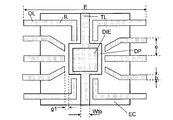
- FIG. 2A shows a schematic view of a lead frame to which a die (semiconductor chip) DIE is fixed.
- the lead frame includes a die pad (die flag), an internal lead IL, an external lead OL, and a tab lead TL.
- a die pad DP is provided at the center of the lead frame, and the die pad DP is supported by a tab lead TL.
- a die (semiconductor chip) DIE is fixed to the die pad DP.
- the internal lead IL is sealed in the resin sealing body EC together with the die pad DP and the tab lead TL, and the external lead OL extends to the outside of the resin sealing body EC.
- the lead frame has a size such as a package length E, a lead pitch e, a lead width b, a tab lead width Wtb, and a lead frame flag gap g1.
- various information regarding these various lead frames are taken into account when calculating the thermal resistivity of the entire package.
- FIG. 2B shows the internal lead frame IL and the external lead frame OL in FIG. 2A to display the die width Wd, die length Ld, die pad width Wf, die pad length Lf, sealing body width E1, and sealing body length D1. Indicates a state that is not. In the present invention, such information is also taken into account when calculating the thermal resistivity and heat capacity of the entire package.
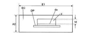
- 3A to 3D show an example of a package cross-sectional view and information thereof, which are considered in step 107 of FIG.
- FIG. 3A shows a state where the die d is fixed on the die pad DP through the die attach (for example, solder) da inside the resin sealing body EC.
- the sealing body thickness A2 and the die thickness td which are the thicknesses of the resin sealing body EC, are taken into account in the calculation of thermal conductivity and thermal resistance.
- the sealing body width E1 and the sealing body length D1 of the resin sealing body EC are considered in step 106, but may be used in step 107 together with the die thickness td for calculation of thermal conductivity and thermal resistance.
- FIG. 3B shows a cross-sectional view of the whole image of the semiconductor integrated circuit according to the present invention, and is also a diagram in which the internal lead IL, the external lead OL, and the bond wire bw are added to FIG. 3A.
- the external lead thickness tl, the lead frame height h of the external lead OL, the lead foot length Lft, the die pad downset ddf which is the distance from the die pad DP to the internal lead IL, and the external lead OL from the bottom of the resin sealing body EC
- the package standoff A1 which is the distance to the end of the wire, and the bond wire bw are used for calculation of thermal conductivity and thermal resistance.
- FIG. 3C shows another semiconductor integrated circuit according to the present invention.
- the die d is placed on the metal placement portion Hra via the die attach da, and the metal placement portion Hra is a land L that is an attachment portion of the board B via the solder s. It is structured to be attached to.
- the volume of the resin sealing body EC is smaller than that of FIG. 3B and the metal mounting portion Hra is provided, the heat generated in the die d passes through the metal mounting portion Hra having a relatively small thermal resistance. Therefore, the heat resistance of the integrated circuit device as a whole is smaller than that in FIG. 3B.
- the thermal resistance and thermal resistance corresponding to the materials and materials of the metal mounting portion Hra, the solder s, the land L, and the board B are calculated.
- FIG. 3D shows the bond wire length Lbw and the bond wire diameter dbw of the bond wire bw shown in FIGS. 3B and 3C.
- the material of the bond wire bw has higher thermal conductivity in the order of aluminum (Al), gold (Au), and copper (Cu). Therefore, the heat transfer is the slowest with three metals of aluminum (Al).
- the thermal conductivity varies with temperature. In general, the lower the temperature, the higher the thermal conductivity of the metal, and the faster the heat conduction.
- thermal simulation is performed in consideration of the thermal conductivity of the bond wire.
- the number of bond wires is used for calculation of the thermal simulation.
- the three-dimensional shape of the package can be created by inputting each piece of information considered in steps 106 and 107 into CAD (computer-aided design) software.
- CAD computer-aided design
- an overall image of the semiconductor integrated circuit can be grasped, and it can be determined whether or not the input of lead frame information and package information to the thermal simulation software is appropriate. That is, one of the features of the present invention is to perform an optimal thermal simulation while grasping a member to be subjected to the thermal simulation in a three-dimensional shape.
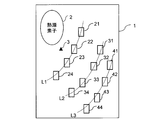
- FIG. 4A and 4B are diagrams for explaining the arrangement in step 110 of FIG. 1 and the temperature distribution on the semiconductor chip, respectively.
- FIG. 4A is an example when the timing element is arranged on the isotherm of the semiconductor chip
- FIG. 4B is a schematic diagram showing the temperature difference between the heat source element and the reference point.
- FIG. 4A shows a state in which the heat source element 2 is arranged at one corner of the semiconductor chip (die) 1 and the reference point 3 is provided in the vicinity of the heat source element 2.
- a monitoring element for measuring a so-called temperature is placed at the reference point 3.
- the first isotherm L1 is formed by connecting a point that is a predetermined temperature, for example, 20 ° C. lower than the center of the heat source element 2.
- the second isotherm L2 is formed by connecting points that are, for example, 20 ° C. lower than the first isotherm L1.
- the third isotherm L3 is formed by connecting points that are, for example, 20 ° C. lower than the second isotherm L2. Therefore, the second isotherms L2 and L3 are formed by connecting points that are 40 ° C. and 60 ° C. lower than the center of the heat source element 2, respectively.
- the first timing elements 21, 22, 23 and 24 are arranged on the first isotherm L1.
- Each of the first timing elements 21 to 24 may be a single transistor or a combination of several transistors, for example, a flip-flop circuit.
- the second timing elements 31, 32, 33 and 34 are disposed on the second isotherm L2. Similarly to the first timing element, the second timing elements 31 to 34 may each be a single transistor, or may be a combination of several transistors, for example, a flip-flop circuit.
- Third timing elements 41, 42, 43 and 44 are arranged on the third isotherm L3. Similarly to the first and second timing elements, the third timing elements 41 to 44 may each be a single transistor, or may be, for example, a flip-flop circuit in which several transistors are combined.
- the circuit block of the logic circuit When the circuit block of the logic circuit is highly integrated, the number of stages of the flip-flop circuits is large, and the same circuit portion extends across the first isotherm L1, the second isotherm L2, and the third isotherm L3.
- a transistor or a flip-flop circuit constituting the circuit must be arranged. In such a case, the arrangement may be determined in consideration of the setup time, hold time, and delay time required for the flip-flop circuit. That is, when the ratio occupied by the timing elements becomes high and it is difficult to place all the timing elements in the vicinity of one isotherm, they may be arranged in the vicinity of a plurality of isotherms.
- the timing elements 21 to 24 are arranged on the isotherm L1
- the timing elements 31 to 34 are arranged on the thermal isotherm L2
- the timing elements 41 to 44 are arranged on the isotherm L3.
- the margin time is the sum of the signal transmission time, the deviation during signal transmission, for example, 10% setup time and hold time, and the delay time resulting from the temperature difference between the elements in the steady state.
- the timing elements 31-34 Provided to operate the timing elements 31-34.
- a sum of a signal transmission time, a deviation time during signal transmission, and a delay time resulting from a temperature difference between the elements in a steady state is provided. Thereby, a margin between the timing elements can be secured by the heat generation of the heat source element 2.
- FIG. 4B is a diagram showing a temporal change in energy generated in the heat source element 2 shown in FIG. 4A and a thermal gradient between the heat source element 2 and the reference point 3 provided in the vicinity of the heat source element 2.
- the axis indicates time t.
- the supplied power When power is supplied to the heat source element 2 at time t0, the supplied power instantaneously has a peak value, so that the heat source element 2 instantaneously generates maximum energy.
- time t1, t2, which is a relatively short time is reached, the magnitude becomes constant at a predetermined magnitude.
- the temperature difference between the heat source element 2 and the reference point 3 here. Since the heat source element 2 gradually generates heat during the period from time t0 to t1, the temperature of the heat source element 2 itself gradually increases. In addition, since the heat transfer from the heat source element 2 is not sufficiently transferred to the reference point 3, the temperature difference between the two gradually increases from time t0 to time t1. At time t1, although the heat source element 2 reaches the maximum temperature, since the heat transfer of the heat source element 2 is not sufficient at the reference point 3, the temperature difference between the two becomes the maximum value Tmax, and the thermal gradient between the two becomes the maximum. .
- the interval from time t0 to t2 is sampled with a pulse signal, and the peak value of the temperature is obtained.
- sampling is performed at a time step in the range of, for example, 1/3 to 1/20 of the RC time constant, which is the product of the thermal resistance R obtained in steps 106 and 107, the lead frame information, and the heat capacity C obtained from the package information.
- the sampling is not performed once.
- the first time may be obtained by narrowing the temperature range roughly at time step 1/3 and then finely sampling the range at time step 1/5, for example.
- the temperature of the heat source element 2 reaches the maximum temperature, and the heat energy generated in the heat source element 2 is transmitted to the reference point 3.
- the temperature difference between the two decreases as the thermal energy transmitted to the reference point 3 increases and is sufficiently propagated at time t2, so that the temperature difference between the two becomes a steady value Tcons.
- the heat distribution and the thermal gradient are not limited to the present invention, and the following can generally be said.
- the balance of heat energy within a unit time is as follows. Is the sum of the amount of heat Q1 flowing through and the amount of heat Q2 taken away by the surrounding convection, and can be expressed by Equation 1 below.
- the amount of heat Q1 generated in the die d within a unit time can be expressed by the following formula 2 according to Fourier's heat conduction law.
- T temperature (K)
- t time (s)
- KT thermal conductivity (W / (m ⁇ K))
- ⁇ density (kg / m 3 )
- CP constant pressure specific heat (J / ( kg ⁇ K))
- ⁇ the Laplace operator
- V the volume (m 3 ).
- A is the area (m 2 )
- h is the heat transfer coefficient (W / m 2 ⁇ k)
- Tm is the ambient temperature (K).
- the arrangement on the isotherm is not limited to the timing element.
- a differential amplifier or a current mirror circuit that requires the same temperature characteristics may be used.
- FIG. 5 is a flowchart illustrating a circuit simulation method for a semiconductor integrated circuit according to the second embodiment of the present invention.
- heat generation or heat transfer of the heat source element is intermittent, or there are a plurality of heat source elements that generate relatively large heat, that is, a steady state does not exist.
- the timing design and the arrangement of the timing elements are based on the maximum value of the temporal deviation between the plurality of timing elements in the semiconductor integrated circuit due to the change in the thermal gradient in the semiconductor integrated circuit due to the heat generated by the heat source element.
- a semiconductor integrated circuit is designed and manufactured.
- FIG. 5 includes steps 201 to 211. Among these steps, each of steps 201 to 207 corresponds to each of steps 101 to 107 of the first embodiment.
- Step 201 is a step of creating a circuit diagram in consideration of circuit operation when designing a circuit in general.
- the target circuit includes a heat source element, various logic circuits, and a timing element depending on the application.
- Examples of the circuit function including such a heat source element include an LED driver, a motor driver, and an IPD (system power supply device).
- Step 202 is a step of circuit simulation of static characteristics and dynamic characteristics along the circuit diagram created in Step 201.
- each node voltage in the circuit a direct current characteristic of a current flowing through each element, a time response characteristic, a frequency response characteristic, and the like are calculated in accordance with the transistor level circuit connection information and the electrical characteristics of the elements in the circuit.
- SPICE Simulation Program with Integrated Circuit Emphasis
- Step 203 is a step of calculating the amount of heat generated by the circuit simulation in Step 202.
- the heat source element and other circuit elements are calculated based on the current flowing in the circuit element during circuit operation and the applied voltage.
- Step 204 is a step of calculating the area of the heating element.
- the circuit simulation at step 202 the current flowing through each circuit element and the applied voltage are obtained, so the area of the heat generating part occupying the entire semiconductor chip is calculated from these data.
- the heat generating portion not only the heat source element but also a relatively large heat generating element is targeted. Obtaining the area of the heat generating portion is not an essential constituent element in the present invention, but is taken into consideration when arranging each circuit element when performing a floor plan described later.
- Step 205 is a step for making a floor plan.
- the temperature distribution in the semiconductor chip is estimated based on the area of the heating element calculated in step 204, and the heat source element, each circuit element, various logic circuits, and each block element are roughly arranged in the semiconductor chip. .
- bonding pads are arranged on the outer periphery of the semiconductor chip to take out the heat source element and each logic circuit.
- Step 206 is a step of inputting “lead frame information” to the thermal simulation software program.
- “lead frame information” for convenience of explanation, but is not necessarily limited to information related to the lead frame.
- the material, diameter, length, etc. of the bond wire may be the target of the thermal simulation.
- the thermal conductivity and thermal resistance are calculated based on the material, material, size, thickness, etc. of the internal lead and external lead of the lead frame.
- the calculation of the thermal conductivity and the thermal resistance can be performed in consideration of the technical ideas disclosed in Patent Documents 2 to 5, but from the viewpoint of the convenience of thermal analysis, for example, the above-mentioned commercially available Use Virtuoso AMS Designer from Cadence Design Systems, USA.
- a schematic diagram of the lead frame and various information of the lead frame related thereto are shown in FIGS. 2A and 2B described above.
- Step 207 is a step for inputting “package information”.
- the term “package information” is also used for convenience as in the “lead frame information” described above.
- the thermal conductivity and thermal resistance of the semiconductor chip itself, and further the thermal conductivity and thermal resistance of the resin body that seals the lead frame are calculated. Further, the thermal conductivity, thermal resistance, and thermal resistance after the above-described lead frame is sealed with the resin body are also calculated. Furthermore, the thermal conductivity and thermal resistance of the bonding wire are calculated based on the diameter and length of the bonding wire connected between the bonding pad on the semiconductor chip and the internal lead. Furthermore, when the die is fixed to some substrate instead of the lead frame, the thermal resistance of the substrate is calculated.
- step 207 If the substrate to which the die is fixed is attached to another substrate, the thermal conductivity and thermal resistance of the other substrate are calculated in step 207.
- the schematic diagram of the package processed in step 207 and the package information related thereto are shown in FIGS. 3A to 3D described above.
- lead frame information is handled in step 206 and package information is handled in step 207.
- package information may be handled in step 206 and lead frame information may be handled in step 207.
- lead frame information and the package information may be input to the thermal simulation software program in one step.
- Step 208 is a step of performing a thermal simulation.
- step 108 of the first embodiment after heat transfer of the heat source element is stabilized, that is, in a steady state, a thermal simulation is performed between the heat source element and the monitor point on the semiconductor chip, but step 208 of the second embodiment. Performs heat simulation in a state where heat generation and heat transfer of the heat source element are changed, that is, in a transient state.
- Step 209 is a step for extracting the maximum thermal gradient in the semiconductor chip.
- the maximum temperature difference between a predetermined position in the semiconductor chip and the reference point is subjected to thermal simulation by the same method as that used in the first embodiment, and the maximum thermal gradient of the entire semiconductor chip is calculated. .
- Step 210 is a step of calculating the worst timing between the timing element to be arranged and another timing element based on the maximum thermal gradient calculated in Step 209.
- the maximum temperature difference Tmax shown in FIG. 4B must be obtained.
- an RC time constant that is a product of the thermal resistance R and the thermal capacity C is obtained from the lead frame information and the package information.
- the temperature difference between times to and t2 is obtained in a time step sufficiently smaller than the RC time constant.
- the time step can be selected, for example, from 1/3 to 1/20 of the time constant RC.
- step 211 the worst timing circuit simulation of the semiconductor integrated circuit is performed in consideration of the worst timing calculated in step 210.
- the worst timing occurs when a margin provided between timing elements reaches a limit value (minimum margin value). Therefore, since the timing element is arranged on the semiconductor chip in consideration of the worst timing, it is possible to prevent a malfunction of the circuit caused by, for example, insufficient margin of the setup time, hold time, and delay time of the timing element.
- the heat source element 2a and the heat source element 2b take into account the on / off timing of the heat source element 2a and the heat source element 2b. Simulate the temperature distribution characteristics of the gradient. That is, for example, when the operation pattern a and the operation pattern b are present, the reference point with the time transition of the heat source element 2a and the heat source element 2b based on the energy of the heat source element 2a and the heat source element 2b at the time of each operation pattern. Calculate the temperature difference from the (monitor point).
- the material conditions in Step 206 and Step 207 may be the best conditions. That is, package external conditions, internal die bonding, and wire bonding are ideal conditions, for example, the thermal resistance is set to a range of, for example, 0 to 0.5 times that of the actual semiconductor integrated circuit (semiconductor The thermal resistance of aluminum (Al), copper (Cu), gold (Au), or a mixture of these with silicon, for example, or a refractory metal material, which is a wiring material used for the internal wiring of the chip) Is selected in the range of 10 to 1 times the actual size, and thermal simulation is performed.
- the maximum temperature difference Tmax can be accurately grasped, and therefore, sufficient margins with timing element setup time, hold time, and delay time can be secured.
- FIG. 6 is a diagram illustrating step 208 of the second embodiment shown in FIG. 5, for example, a case where heat generation of the heat source element 2 of FIG. 4A occurs intermittently.
- the heat source element 2 is a high-side transistor of a DC / DC converter (not shown)
- the high-side transistor is generally controlled to be turned on / off by a drive signal of pulse width modulation (PWM, Plus Width Modulation).
- PWM pulse width modulation
- the drive signal for controlling the heat source element 2 has substantially the same waveform.
- the drive signal is at the high level H, the heat source element 2 is turned on, and energy is consumed.
- the drive signal is at the low level L, the heat source element 2 is turned off, and the operation is stopped.
- FIG. 6 is a diagram showing a change in temperature difference between the reference point 3 and the heat source element 2 when the heat energy of the heat source element 2 changes as in the upper part of FIG.
- the temperature difference between the reference point 3 and the heat source element 2 rises at time t11 to t12, t13 to t14, t15 to t16, and time t17 to t18, and from time t12 to t13, t14 to t15, t15 to t16, and after time t18. To descend.
- the temperature difference calculation method in this case is the same as the temperature difference calculation method obtained in the first embodiment.
- the temperature difference becomes the maximum ⁇ Tmax at times t12, t14, and time t16. Note that the time at which the maximum temperature difference ⁇ Tmax occurs exists in addition to the times t12, t14, and t16.
- FIG. 7 is a flowchart showing a circuit simulation method for a semiconductor integrated circuit according to the third embodiment.
- the third embodiment is applied, for example, when applied to circuit simulation of the semiconductor integrated circuit designed and manufactured in the first embodiment or the second embodiment of the present invention. That is, the third embodiment is used when verifying whether or not the arrangement of the timing elements in the already manufactured and completed semiconductor integrated circuit is appropriate.
- the third embodiment includes steps 301 to 310, but each of steps 301 to 304 is the same as each of steps 201 to 204 in the second embodiment.
- Step 301 is a step of creating a circuit diagram in consideration of circuit operation when designing a circuit in general.
- the target circuit includes a heat source element, various logic circuits, and a timing element depending on the application.
- Examples of the circuit function including such a heat source element include an LED driver, a motor driver, and an IPD (system power supply device).
- Step 302 is a step for circuit simulation of static characteristics and dynamic characteristics along the circuit diagram created in step 301.
- each node voltage in the circuit a direct current characteristic of a current flowing through each element, a time response characteristic, a frequency response characteristic, and the like are calculated in accordance with the transistor level circuit connection information and the electrical characteristics of the elements in the circuit.
- SPICE Simulation Program with Integrated Circuit Emphasis
- Step 303 is a step of calculating the amount of heat generated by the circuit simulation in Step 302.
- the heat source element and other circuit elements are calculated based on the current flowing in the circuit element during circuit operation and the applied voltage.
- Step 304 is a step of calculating the area of the heating element.
- the current flowing through each circuit element and the applied voltage are obtained, so the area of the heat generating part occupying the entire semiconductor chip is calculated from these data.
- the heat generating portion not only the heat source element but also a relatively large heat generating element is targeted. Obtaining the area of the heat generating portion is not an essential constituent element in the present invention, but is taken into consideration when arranging each circuit element when performing a floor plan described later.
- Steps 305 to 307 are the same as steps 206 to 208 in the second embodiment.
- step 105 in the first embodiment and step 205 in the second embodiment are not necessary.
- Step 306 is a step of inputting “lead frame information” to the thermal simulation software program.
- “lead frame information” for convenience of explanation, but is not necessarily limited to information related to the lead frame.
- the material, diameter, length, etc. of the bond wire may be subjected to thermal simulation.
- the thermal conductivity and thermal resistance are calculated based on the material, material, size, thickness, etc. of the internal lead and external lead of the lead frame.
- the calculation of the thermal conductivity and the thermal resistance can be performed in consideration of the technical ideas disclosed in Patent Documents 2 to 5, but from the viewpoint of the convenience of thermal analysis, for example, the above-mentioned commercially available Use Virtuoso AMS Designer from Cadence Design Systems, USA.
- a schematic diagram of the lead frame and various information of the lead frame related thereto are shown in FIGS. 2A and 2B described above.
- Step 307 is a step for inputting “package information”.
- the term “package information” is also used for convenience as in the “lead frame information” described above.
- the thermal conductivity and thermal resistance of the semiconductor chip itself, and further the thermal conductivity and thermal resistance of the resin body that seals the lead frame are calculated. Further, the thermal conductivity and thermal resistance after the above-described lead frame is sealed with the resin body are also calculated. Furthermore, the thermal conductivity and thermal resistance of the bonding wire are calculated based on the diameter and length of the bonding wire connected between the bonding pad on the semiconductor chip and the internal lead. Furthermore, when the die is fixed to some substrate instead of the lead frame, the thermal resistance of the substrate is calculated.
- step 307 If the substrate on which the die is fixed is attached to another substrate, the thermal conductivity and thermal resistance of the other substrate are calculated in step 307.
- the schematic diagram of the package processed in step 307 and the package information related thereto are shown in FIGS. 3A to 3D described above.
- the lead frame information is handled in step 306 and the package information is handled in step 307.
- the order of these processing steps may be reversed. That is, package information may be handled in step 306 and lead frame information may be handled in step 307. Further, the lead frame information and the package information may be input to the thermal simulation program in one step.
- Step 308 is a step for performing a thermal simulation.
- a heat simulation between the heat source element 2 and the reference point 3 (monitor point) on the semiconductor chip is performed after the heat transfer of the heat source element is stabilized, that is, in a steady state.
- thermal simulation is performed in a state where heat generation and heat transfer of the heat source element 2 are changed, that is, in a transient state.
- Step 308 is a step for extracting the position maximum thermal gradient from the thermal gradient for each time and each pattern calculated in Step 307. Comparing step 308 with step 209 in the second embodiment, the implementation method is the same, but the accuracy of the obtained thermal gradient is different.
- the arrangement of circuit elements in the second embodiment is a rough floor plan, and simulation is performed with a rough arrangement, whereas in the third embodiment, circuit simulation is performed after arrangement of circuit elements, particularly timing elements, is completed. Therefore, since the setup time, hold time, etc. can be accurately grasped, these margin settings can be utilized in the design and manufacture of the next semiconductor integrated circuit.
- Step 309 is a step of feeding back the setup time, hold time, and delay time information based on the maximum thermal gradient obtained in Step 308 to each circuit element, particularly the timing element. For example, when there is a temperature difference between timing elements with signal transmission, a time delay due to the temperature difference is converted into a time constant R1C1 and fed back. Such feedback enables more accurate circuit simulation.
- Step 310 is a step of performing a final circuit simulation after replacing the delay time obtained in Step 309 with the time constant R1C1.
- This circuit simulation may be performed statically or dynamically. According to such circuit simulation and thermal simulation, it is possible to accurately grasp the delay time of the data signal and the clock signal input to the timing element.
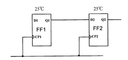
- FIG. 8A and 8B are conceptual diagrams showing time constants applied in steps 308 and 309 of the third embodiment.
- FIG. 8A since the D flip-flop FF1 and the D flip-flop FF2 are both placed at a temperature of 25 ° C., there is no temperature difference between them. In this case, the time constant interposed between the two is zero.
- FIG. 8B shows a state where the D flip-flop FF1a is placed at a temperature of 25 ° C. and the D flip-flop FF1b is placed at a temperature of 80 ° C. In such a case, a temperature difference of 55 ° C. occurs between the two.
- Each D flip-flop has an input terminal CP1, a D input terminal D1, and Q output terminals Q1 and Q2.
- the semiconductor integrated circuit arrangement method and circuit simulation method according to the present invention accurately set the setup time, hold time, and delay time of the timing element including the heat source element based on the lead frame information and the package information. Since it can be grasped, it is possible to provide a semiconductor integrated circuit whose circuit operation is stable with respect to a temperature change. Therefore, its industrial applicability is extremely high.
Landscapes
- Engineering & Computer Science (AREA)
- Physics & Mathematics (AREA)
- Theoretical Computer Science (AREA)
- Computer Hardware Design (AREA)
- Evolutionary Computation (AREA)
- Geometry (AREA)
- General Engineering & Computer Science (AREA)
- General Physics & Mathematics (AREA)
- Architecture (AREA)
- Design And Manufacture Of Integrated Circuits (AREA)
- Semiconductor Integrated Circuits (AREA)
Abstract
半導体集積回路の配置方法は、回路図を作成するステップ(101)と、回路動作シミュレーションをするステップ(102)と、 回路動作シミュレーションにより前記熱源素子の発熱量を算出するステップ(103)と、回路配置のフロアープランを行うステップ(105)と、リードフレーム情報及びパッケージ情報に基づき熱抵抗を算出するステップ(106),(107)と、算出した熱抵抗に基づき熱シミュレーションをするステップ(108)と、熱シミュレーションに基づき等温線(熱分布)を作成するステップ(109)と、等温線に沿ってタイミング素子を置くステップ(110)と、を備える。
Description
本発明は、半導体集積回路の配置方法、回路シミュレーション方法、及び、その配置方法または回路シミュレーション方法に基づいて設計ないし製造される半導体集積回路に関する。
たとえば、各種ドライバ集積回路、電源集積回路、CPU(中央処理装置)、IPD(インテリジェントパワーデバイス)等の大電流が流れる熱源素子を内蔵する半導体集積回路の配置には、従前、熱対策が講じられるものが少なくない。
特許文献1は、2つ以上の温度依存素子の温度変化がほぼ同一となるよう、熱源素子及び温度依存素子を配置する方法を開示する。
特許文献2は、消費電力を多く発生する回路ブロックを半導体基板上に分散配置することにより、半導体基板上の温度分布を均一化するという、半導体集積回路の自動配置方法を開示する。そのために、基本論理回路を機能ごとにグループ化して回路ブロックとし、複数の回路ブロックを半導体基板上に自動配置する方法において、回路動作をシミュレーションして得られたシミュレーション出力結果と、基本論理回路の消費電力を計算する手段を格納した消費電力計算ルールファイルとを用いて回路ブロックの消費電力を計算する。この計算結果と回路接続情報と半導体基板上に基本論理回路を配置および配線するときの配置制約手段とを用いて、半導体基板上に単位面積当たりの消費電力を平均化するように回路ブロックを配置するものである。
特許文献3は、表面実装型素子よりの放熱経路の熱抵抗算出方法を開示する。こうした熱抵抗算出方法を手立てとして設計することにより熱に関して信頼性の高いものを設計し、製造することができるとしている。
特許文献4は、半導体集積回路の大規模化、高集積化に際しても作業性よく半導体集積回路の設計を行い、熱特性に優れた半導体集積回路システムを設計する方法を提供するとしている。そのために、システム仕様情報に基づき、そのシステムを収納する筐体および、筐体内に収納され、そのシステムを構成する実装基板と、実装基板上に実装されるパッケージ基板を含む半導体集積回路(LSI)装置の設計を行う第1の工程と、第1の工程で得られた設計結果に基づき、筐体内における実装基板および半導体集積回路の少なくとも一方の熱解析を行う工程と、熱解析を行う工程の解析結果に基づき半導体集積回路システムを設計する第2の工程を含んでいる。特許文献4によれば、半導体集積回路の素子配置を、半導体集積回路の内部条件のみならず、筐体を含む実装基板およびパッケージ基板の熱解析情報に基づいて最適化することで、実装基板、パッケージ基板、半導体集積回路全体の最適化を実施することが可能となるとしている。
特許文献5は、電子回路の配置設計を行うにあたり熱源の位置情報を考慮するものであり、これによって、最適な電気的特性が得られるとしている。そのために、複数の回路ブロックと、少なくとも1つの熱源を含む電子回路の配置を作成する電子回路の配置作成装置において、第1の回路ブロックのネットリストを含む回路ネットリストデータと、回路ネットリストデータに基づいて回路シミュレーションを行う。シミュレーション結果データに基づいて、熱源を検索して熱源位置を算出する熱源位置算出手段と、算出された熱源位置と、予め入力されたフロアープランによる全回路ブロックの配置情報から、各回路ブロックからの熱源の相対位置を算出する熱源相対位置を算出する熱源相対位置算出手段と、第1の回路ブロックとは異なる第2の回路ブロックの配置作成時に、算出された熱源の相対位置に基づいて、熱源のシンボルを、指定された第2の回路ブロックの相対位置に表示するように制御する配置熱源表示制御手段とを備える。
特許文献1は、熱源素子と温度依存素子が併存する半導体集積回路において温度依存素子相互の熱的整合性を向上させることはできる。しかし、半導体チップの大きさや厚み、さらには半導体基板が実装されるパッケージ等の熱抵抗は考慮していない。このため、半導体チップ内の熱分布、熱勾配に沿って適確に配置したとは言えない。
特許文献2は、その段落0025に半導体チップとパッケージを含んだ熱伝導のシミュレーションを実行してチップ内の単位面積当たりのチップ温度を求め、チップ上の最高温度Tmaxと最低温度Tminの差が許容温度Tc内にはいっているかどうかを計算し、許容温度Tc内に入っていない場合、回路ブロックを再度分割して消費電力の分散を計ることを示唆する。しかし、熱伝導率、熱抵抗の具体的なシミュレーション方法についてまでは開示も示唆もしていない。
特許文献3は、半導体チップとパッケージの熱抵抗を求めることを開示するが、回路素子を半導体チップ上に配置する配置方法までは開示も示唆もしていない。
特許文献4は、半導体集積回路システムの設計に際し、熱解析を行った後、この解析結果に基づき、半導体集積回路の素子配置、あるいは、パッケージ基板への実装構造、実装基板上での配置などを決定しているため、熱特性に優れた半導体集積回路システムの実現を図ることは期待できる。しかし、熱解析の対象が半導体チップのサイズや厚み、ボンディングワイヤーの径や長さ、ダイパッド(ダイフラグ)のサイズなどを考慮していないので、半導体チップ内での適正な熱分布、熱勾配を把握することは期待できない。
特許文献5は、熱源位置算出手段により電子回路全体のうち熱源を含む回路ブロックのネットリストデータと、そのシミュレーション結果に基づいて、回路ブロック中に発生する熱源を特定して熱源位置を算出することが可能となるため、熱源の判断漏れが起こることはない。しかし、特許文献4と同様に、熱解析の対象が半導体チップのサイズや厚み、ボンディングワイヤーの径や長さ、ダイパッドのサイズなどを考慮していないので、半導体チップ内での正確な熱分布を把握することは期待できない。
本発明の目的は、上記の問題点、不具合を克服するものである。そのために、半導体チップに作り込まれた熱源素子の大きさ(面積)、消費電力を初め、半導体チップのサイズ、ボンディングワイヤーの径や長さ、ダイパッド(ダイフラグ)のサイズ、半導体チップを封止するパッケージのサイズ、形状、材料、材質などの熱伝導率の算出を行う。そして、それらの算出結果に基づき、半導体チップ内の温度分布、温度勾配を求め、その温度分布や温度勾配に基づき、半導体集積回路(半導体チップ)内に各種回路素子の配置または回路シミュレーションを行い、半導体集積回路を設計ないし製造するものである。
本書において、「タイミング素子」とは、論理回路に用いられるトランジスタまたは論理回路を指す。論理回路の代表としてフリップフロップ回路を挙げることができる。また、「リードフレーム情報」とは半導体チップが搭載される金属細条であるリードフレームに関する形状、材料、材質、各種の物理的な特性及びこれらのサイズ、厚み等の少なくとも1つを指す。また、「パッケージ情報」とは、リードフレームの一部及び半導体チップを封止する封緘体の形状、材料、材質、各種の物理的定数や特性及びこれらのサイズ、厚み等の少なくとも1つを指す。物理的な特性には、リードフレーム情報、パッケージ情報に関わらず、代表的には熱伝導率、熱抵抗、熱容量を挙げることができる。また、本書で「半導体チップ」は、半導体集積回路が作り込まれた半導体基板を小さく分割した小片を指す。また、「等温線」とは半導体チップ上で同じ温度の地点を結んで得られる、いわゆる温度分布線を指す。
本発明に係る半導体集積回路の配置方法は、
(a)半導体集積回路の回路図を作成するステップと、
(b)前記回路図に基づき前記半導体集積回路の回路動作シミュレーションを行うステップと、
(c)前記回路動作シミュレーションに基づき、前記半導体集積回路の発熱量を算出するステップと、
(d)前記算出した発熱量を参照して前記半導体集積回路のフロアープランを行うステップと、
(e)前記フロアープランに沿って前記半導体集積回路が搭載されるリードフレーム情報及び前記半導体集積回路が封止されるパッケージ情報に基づき熱抵抗を算出するするステップと、
(f)前記算出した熱抵抗に基づき前記パッケージに封止された半導体集積回路全体の熱シミュレーションを行うステップと、
(g)前記熱シミュレーションの結果に基づき前記半導体集積回路の等温線(温度分布線)を作成するステップと、
(h)前記等温線に沿って少なくともタイミング素子を半導体チップ上に配置するステップ、とを備えている。
(a)半導体集積回路の回路図を作成するステップと、
(b)前記回路図に基づき前記半導体集積回路の回路動作シミュレーションを行うステップと、
(c)前記回路動作シミュレーションに基づき、前記半導体集積回路の発熱量を算出するステップと、
(d)前記算出した発熱量を参照して前記半導体集積回路のフロアープランを行うステップと、
(e)前記フロアープランに沿って前記半導体集積回路が搭載されるリードフレーム情報及び前記半導体集積回路が封止されるパッケージ情報に基づき熱抵抗を算出するするステップと、
(f)前記算出した熱抵抗に基づき前記パッケージに封止された半導体集積回路全体の熱シミュレーションを行うステップと、
(g)前記熱シミュレーションの結果に基づき前記半導体集積回路の等温線(温度分布線)を作成するステップと、
(h)前記等温線に沿って少なくともタイミング素子を半導体チップ上に配置するステップ、とを備えている。
また、本発明に係る半導体集積回路の回路シミュレーション方法は、
(a)熱源素子を含む半導体集積回路の回路図を作成するステップと、
(b)前記回路図に基づき前記半導体集積回路の回路動作シミュレーションを行うステップと、
(c)前記回路動作シミュレーションに基づき、前記半導体集積回路の発熱量を算出するステップと、
(d)前記算出した発熱量を参照して前記半導体集積回路のフロアープランを行うステップと、
(e)前記半導体集積回路が搭載されるリードフレーム及び前記半導体集積回路が封止されるパッケージの各種情報に基づき熱抵抗を熱シミュレーションソフトに入力するステップと、
(f)前記熱抵抗に基づき前記半導体集積回路が前記パッケージに封止された半導体集積回路全体の熱シミュレーションを行うステップと、
(g)前記熱シミュレーションの結果に基づき最大熱勾配差を算出するステップと、
(h)前記算出した熱勾配差に基づき前記半導体集積回路を構成するタイミング素子のワーストタイミングを算出するステップと、
(i)前記ワーストタイミングに基づき前記ワーストタイミングで回路シミュレーションを行うステップとを備えている。
(a)熱源素子を含む半導体集積回路の回路図を作成するステップと、
(b)前記回路図に基づき前記半導体集積回路の回路動作シミュレーションを行うステップと、
(c)前記回路動作シミュレーションに基づき、前記半導体集積回路の発熱量を算出するステップと、
(d)前記算出した発熱量を参照して前記半導体集積回路のフロアープランを行うステップと、
(e)前記半導体集積回路が搭載されるリードフレーム及び前記半導体集積回路が封止されるパッケージの各種情報に基づき熱抵抗を熱シミュレーションソフトに入力するステップと、
(f)前記熱抵抗に基づき前記半導体集積回路が前記パッケージに封止された半導体集積回路全体の熱シミュレーションを行うステップと、
(g)前記熱シミュレーションの結果に基づき最大熱勾配差を算出するステップと、
(h)前記算出した熱勾配差に基づき前記半導体集積回路を構成するタイミング素子のワーストタイミングを算出するステップと、
(i)前記ワーストタイミングに基づき前記ワーストタイミングで回路シミュレーションを行うステップとを備えている。
また、本発明に係る半導体集積回路の回路シミュレーション方法は、
(a)熱源素子を含む半導体集積回路の回路図を作成するステップと、
(b)前記回路図に基づき前記半導体集積回路の回路動作シミュレーションを行うステップと、
(c)前記回路動作シミュレーションに基づき、前記半導体集積回路の発熱量を算出するステップと、
(d)前記半導体集積回路が搭載されるリードフレーム情報及び前記半導体集積回路が封止されるパッケージの情報に基づき熱抵抗を算出するステップと、
(e)前記熱抵抗に基づき前記パッケージに封止された半導体集積回路全体の熱シミュレーションを行うステップと、
(f)前記熱シミュレーションの結果に基づき最大熱勾配時の熱分布情報を抽出するステップと、
(g)前記抽出した熱分布情報を、前記半導体集積回路を構成するタイミング素子にフィードバックするステップと、
(h)前記フィードバックした熱分布情報に基づき回路シミュレーションを行うステップ、とを備えている。
(a)熱源素子を含む半導体集積回路の回路図を作成するステップと、
(b)前記回路図に基づき前記半導体集積回路の回路動作シミュレーションを行うステップと、
(c)前記回路動作シミュレーションに基づき、前記半導体集積回路の発熱量を算出するステップと、
(d)前記半導体集積回路が搭載されるリードフレーム情報及び前記半導体集積回路が封止されるパッケージの情報に基づき熱抵抗を算出するステップと、
(e)前記熱抵抗に基づき前記パッケージに封止された半導体集積回路全体の熱シミュレーションを行うステップと、
(f)前記熱シミュレーションの結果に基づき最大熱勾配時の熱分布情報を抽出するステップと、
(g)前記抽出した熱分布情報を、前記半導体集積回路を構成するタイミング素子にフィードバックするステップと、
(h)前記フィードバックした熱分布情報に基づき回路シミュレーションを行うステップ、とを備えている。
また、本発明に係る半導体集積回路は、上記の配置方法ないし回路シミュレーション方法に基づいて設計ないし製造される。
本発明に係る半導体集積回路の配置方法ないし回路シミュレーション方法は、半導体チップに作り込まれる熱源素子の電力の大きさ、半導体チップが搭載されるリードフレーム及びパッケージの熱伝導率、熱抵抗の大きさに基づき半導体チップ内の温度分布、温度勾配を実態に即して把握し、回路素子を配置するので、温度特性に優れた半導体集積回路を設計ないし製造することができる。
(第1実施形態)
図1は、本発明に係る第1実施形態の半導体集積回路の配置方法を説明するフローチャートである。ステップ101は、一般的に回路を設計する際に、回路動作を考慮して、回路図を作成するステップである。対象となる回路の中には用途に応じて熱源素子や各種論理回路が含まれる。こうした熱源素子を含む回路機能としては、たとえば、LEDドライバ、モータドライバ、IPD(システム電源装置)等を挙げることができる。
図1は、本発明に係る第1実施形態の半導体集積回路の配置方法を説明するフローチャートである。ステップ101は、一般的に回路を設計する際に、回路動作を考慮して、回路図を作成するステップである。対象となる回路の中には用途に応じて熱源素子や各種論理回路が含まれる。こうした熱源素子を含む回路機能としては、たとえば、LEDドライバ、モータドライバ、IPD(システム電源装置)等を挙げることができる。
ステップ102は、ステップ101で作成した回路図に沿って、静特性、動特性を回路シミュレーションするステップである。回路シミュレーションではトランジスタレベルの回路接続情報と回路内の素子の電気的特性に従って、回路内の各ノード電圧、各素子に流れる電流の直流特性や、時間応答特性、周波数応答特性などが算出される。回路シミュレーション、熱解析回路シミュレーションには、たとえば、SPICE(Simulation Program with Integrated Circuit Emphasis)や米国、メンターグラフィック社のAdvanced-MSなどを用いることができる。
ステップ103は、ステップ102での回路シミュレーションにより発熱量を算出するステップである。すなわち、回路動作時の回路素子に流れる電流と印加される電圧、及び消費電力を熱源素子及びそれ以外の回路素子も含めて算出する。
ステップ104は、発熱部の面積を算出するステップである。ステップ102の回路シミュレーションでは各素子に流れる電流と印加される電圧が求まっているので、それらのデータから半導体チップ全体に占める発熱部の面積を計算する。発熱部の大半は熱源素子(パワートランジスタ)である。ステップ104は本発明では必須の構成要件ではないが、発熱部の面積を算出することにより熱容量を求めることができ、熱シミュレーション精度を高めることができる。発熱部面積の算出結果は後述のフロアープランで各回路素子を半導体チップ上に配置するときに配慮される。なお、ステップ104はステップ103の後ではなく、その前に行ってもよい。
ステップ105は、フロアープランを行うステップである。フロアープランでは、ステップ104で算出された発熱体の面積に基づき、半導体チップ内の温度分布を推定し、半導体チップ内に熱源素子、各回路素子、各種論理回路、各ブロック素子を大まかに配置する。また、フロアープランでは半導体チップの外周辺に熱源素子や各論理回路を外部に取り出すためにボンディングパッドが配置される。
ステップ106は、熱シミュレーションソフトプログラムに「リードフレーム情報」を入力するステップである。本書では説明の便宜上「リードフレーム情報」として記述するが、必ずしもリードフレームに関わる情報だけに限定されない。たとえば、ステップ106ではボンドワイヤーの材質、径、長さ等を熱シミュレーションの対象としてもかまわない。ステップ106ではおもにリードフレームの熱伝導率、熱抵抗を算出するためにリードフレームの内部リード、外部リードそれぞれの材料、材質、サイズ、厚み等に基づき熱伝導率、熱抵抗が算出される。なお、熱伝導率や熱抵抗の算出にあたっては、特許文献2~5に開示された技術思想を考慮しながら行うことができるが、熱分析の便宜性からみると、市販されているたとえば、上記米国ケイデンス・デザイン・システムズ社のVirtuoso AMS Designerを用いると良い。ステップ106では、リードフレームの熱容量が算出できると共に半導体チップからリードフレームへの熱抵抗が算出される。なお、リードフレームの模式図およびそれに関わるリードフレームの各種情報は、後述の図2に示される。
ステップ107は、「パッケージ情報」を入力するステップである。パッケージ情報なる語句も先に説明した「リードフレーム情報」と同様に便宜上用いている。ステップ107のパッケージ情報では、半導体チップ自体の熱伝導率、熱抵抗、さらにはリードフレームを封止する樹脂体の熱伝導率、熱抵抗、熱容量等を算出する。さらに先に述べたリードフレームが樹脂体に封止された後の熱伝導率、熱抵抗、熱容量も算出する。さらに、半導体チップ上のボンディングパッドと内部リードとの間に結線されるボンドワイヤーの径、長さに基づきボンディングワイヤーの熱伝導率、熱抵抗が算出される。さらに、ダイがリードフレームではなく、何らかの基板に固着される場合には、その基板の熱抵抗が算出される。また、ダイが固着された基板がさらに別の基板に取り付けられる構成下の場合には、その別の基板の熱伝導率、熱抵抗の算出をステップ107で行う。ステップ107では、パッケージの熱容量が算出できると共にリードフレームからパッケージへの熱抵抗が算出される。なお、ステップ107で処理されるパッケージの模式図及びそれに関わるパッケージ情報は後述の図3A~図3Dに示される。
なお、第1実施形態ではステップ106でリードフレーム情報を扱い、ステップ107でパッケージ情報を扱ったが、これらの処理ステップの順序は逆転しても構わない。すなわち、ステップ106でパッケージ情報を扱い、ステップ107でリードフレーム情報を扱ってもかまわない。また、リードフレーム情報とパッケージ情報を1つのステップで熱シミュレーションソフトプログラムに入力してもかまわない。
ステップ108は、ステップ106でのリードフレーム情報及びステップ107でのパッケージ情報により算出した熱抵抗の大きさに基づき、半導体集積回路全体の熱解析(熱シミュレーション)を行う。ステップ108は、定常解析、すなわち、回路動作が安定し、半導体チップ(ダイ)内の熱分布が落ち着いた状態で熱シミュレーションが行われる。
ステップ109は、ステップ108で行った熱シミュレーション(定常解析)に基づき、半導体チップ(半導体集積回路)内の等温線を作成するステップである。等温線は半導体チップ上の同じ温度の地点を結んで得られる、いわゆる温度分布線である。同じ温度と言ってもある程度の幅をもたせて作成するのが実用的である。作成する等温線の数は、半導体チップ上の最大温度及び最小温度それぞれの絶対値と、それらの間の温度差に基づき決定すればよい。たとえば、半導体チップ上の最大温度が150℃で、最小温度が50℃である場合には、たとえば、20℃の間隔で、等温線を作成するとすれば、その数は6本となる。等温線は自動または手動で作成される。
ステップ110は、ステップ109で作成した等温線に沿って半導体チップ上にタイミング素子を配置する。ここで、タイミング素子とは、論理回路を構成するトランジスタ、ダイオード、抵抗等を指す。たとえば、論理回路において、クロック信号を供給する方法として、一括駆動方式、クロック・ツリー方式、これら両者の組み合わせ方式等が知られているが、タイミング素子としては、これらに用いるクロックドライバ、フリップフロップ回路を挙げることができる。もちろん、フリップフロップ回路を構成する各トランジスタもタイミング素子に該当する。なお、フリップフロップ回路のセットアップ時間、ホールド時間、遅延時間は論理回路の動作に大きな影響を与えるので、温度変化に対して十分な配慮が必要となる。
図2A及び図2Bは、図1のステップ106で考慮されるリードフレーム情報の一例を示す。図2Aは、ダイ(半導体チップ)DIEが固着されるリードフレームの概略図を示す。本書でリードフレームはダイパッド(ダイフラグ)、内部リードIL、外部リードOL、及びタブリードTLで構成される。リードフレームの中央部にはダイパッドDPが設けられ、ダイパッドDPはタブリードTLで支持されている。ダイパッドDPにはダイ(半導体チップ)DIEが固着される。内部リードILはダイパッドDP、タブリードTLと共に樹脂封止体ECの中に封止され、外部リードOLは樹脂封止体ECの外側に延出している。リードフレームは、パッケージ長E、リードピッチe、リード幅b、タブリード幅Wtb、リードフレームフラッグギャップg1などのサイズを有する。本発明では、こうした各種リードフレームに関する各種情報がパッケージ全体の熱抵抗率を計算するときに考慮される。
図2Bは、ダイ幅Wd、ダイ長Ld、ダイパッド幅Wf、ダイパッド長Lf、封止体幅E1、封止体長D1を表示するために図2Aにおいての内部リードフレームILおよび外部リードフレームOLを示していない状態を示す。本発明では、こうした情報もパッケージ全体の熱抵抗率、熱容量を計算するときに考慮される。
図3A~図3Dは、それぞれ、図1のステップ107で考慮される、パッケージの断面図及びその情報の一例を示す。
図3Aは、樹脂封止体ECの内部にダイdがダイパッドDP上にダイアタッチ(たとえば半田)daを介して固着された状態を示す。図3Aでは、樹脂封止体ECの厚みである封止体厚A2及びダイ厚tdが熱伝導率、熱抵抗の算出に考慮される。なお、樹脂封止体ECの封止体幅E1、封止体長D1をステップ106で考慮したが、ステップ107でダイ厚tdと共に熱伝導率、熱抵抗の算出に用いてもよい。
図3Bは、本発明に係る半導体集積回路の全体像の断面図を示すが、図3Aに、内部リードIL、外部リードOL、及びボンドワイヤーbwを加えた図でもある。図3Bでは、外部リード厚tl、外部リードOLのリードフレーム高h、リードフット長Lft、ダイパッドDPから内部リードILまでの距離であるダイパッドダウンセットddf、樹脂封止体ECの底部から外部リードOLの端部までの距離であるパッケージスタンドオフA1、及びボンドワイヤーbwが、熱伝導率、熱抵抗の算出に用いられる。
図3Cは、本発明に係る別の半導体集積回路を示す。図3Cは、図3Bとは異なり、ダイdがダイアタッチdaを介して金属載置部Hraに載置され、さらに金属載置部Hraが半田sを介してボードBの取り付け部であるランドLに装着される構造を成している。図3Cは、樹脂封止体ECの体積が図3Bのそれよりも小さく、かつ、金属載置部Hraを設けたのでダイdでの発熱は熱抵抗が比較的小さな金属載置部Hraを介して急速に外部に放熱されるので、図3Bよりは集積回路装置全体の熱抵抗は小さくなる。図3Cでは、金属載置部Hra、半田s、ランドL、及びボードBの材質、材料に応じた熱抵抗率、熱抵抗が算出される。
図3Dは、図3B、図3Cに示したボンドワイヤーbwのボンドワイヤー長Lbw、ボンドワイヤー径dbwを示す。ボンドワイヤーbwの材料は、アルミニウム(Al)、金(Au)、銅(Cu)の順に熱伝導率は高くなる。したがって、アルミニウム(Al)が3つの金属では熱の伝わり方が一番遅い。また、熱伝導率は温度によっても変化する。一般的に金属は温度が低いほど熱伝導率が高くなり、熱伝導が速くなる。本発明ではこうしたボンドワイヤーの熱伝導率も考慮して熱シミュレーションを行う。なお、ボンドワイヤーbwは材料、径、長さのほかにボンドワイヤーの数も熱シミュレーションの算出に用いる。
なお、ステップ106,107で考慮した各情報をキャド(CAD、computer-aided design)ソフトに入力することで、パッケージの三次元形状を作成することができる。三次元形状を把握することで、半導体集積回路の全体像を掴むことができ、リードフレーム情報及びパッケージ情報の熱シミュレーションソフトへの入力が適切であるか否かを判断することができる。すなわち、熱シミュレーションの対象となる部材を三次元形状で把握しながら最適な熱シミュレーションを行うのが本発明の1つの特徴でもある。
図4A及び図4Bは、それぞれ、図1のステップ110での配置と半導体チップ上の温度分布を説明する図である。図4Aは、半導体チップの等温線上にタイミング素子を配置したときの一例を、図4Bは、熱源素子から基準点との間の温度差をそれぞれ示した模式図である。
図4Aは、半導体チップ(ダイ)1の片隅に熱源素子2が配置され、熱源素子2の近傍に基準点3を設けた状態を示す。基準点3には、いわゆる温度を測定するためのモニター素子が置かれる。第1の等温線L1は熱源素子2の中心部から所定の温度、たとえば20℃低い地点が結ばれて形成されている。第2の等温線L2は第1の等温線L1より、たとえば20℃低い地点が結ばれて形成されている。第3の等温線L3は第2の等温線L2より、たとえば20℃低い地点が結ばれて形成されている。したがって、第2の等温線L2,L3は、熱源素子2の中心部からそれぞれ40℃,60℃低い地点が結ばれて形成されている。
第1の等温線L1上には、第1のタイミング素子21,22,23及び24が配置されている。第1のタイミング素子21~24は、それぞれトランジスタ単体であったり、或いはトランジスタがいくつか組み合わされた、たとえばフリップフロップ回路であったりする。
第2の等温線L2上には第2のタイミング素子31,32,33及び34が配置されている。第2のタイミング素子31~34は、第1のタイミング素子と同様にそれぞれトランジスタ単体であったり、或いはトランジスタがいくつか組み合わされた、たとえばフリップフロップ回路であったりする。
第3の等温線L3上には第3のタイミング素子41,42,43及び44が配置されている。第3のタイミング素子41~44は、第1,第2のタイミング素子と同様にそれぞれトランジスタ単体であったり、或いはトランジスタがいくつか組み合わされた、たとえばフリップフロップ回路であったりする。
論理回路の回路ブロックが高集積に亘る場合にはフリップフロップ回路の段数も多数となり、第1の等温線L1、第2の等温線L2、及び第3の等温線L3にまたがって、同じ回路部を構成するトランジスタやフリップフロップ回路を配置しなければならない場合が発生する。こうした場合には、フリップフロップ回路に要求されるセットアップ時間、ホールド時間、及び遅延時間を考慮して配置を決めるとよい。すなわち、タイミング素子が占める割合が高くなり、全てのタイミング素子を1つの等温線の近辺に置くことが困難の場合には、複数の等温線の近辺に配置しても良い。たとえばタイミング素子21~24を等温線L1に配置し、タイミング素子31~34を熱等温線L2に配置し、タイミング素子41~44を等温線L3に配置する。タイミング素子21~24の動作完了後、信号の伝達時間と、信号伝達中のズレたとえば10%のセットアップ時間及びホールド時間と、定常時の素子間の温度差から生じる遅延時間の和をマージン時間として設けて、タイミング素子31~34を動作させる。同じく、タイミング素子31~34とタイミング素子41~44の間も信号の伝達時間と、信号伝達中のズレ時間と、定常時の素子間の温度差から生じる遅延時間の和を設ける。それによって、熱源素子2の発熱により、タイミング素子間のマージンを確保することができる。
図4Bは、図4Aに示した熱源素子2で生じるエネルギーの経時変化と、熱源素子2と、熱源素子の2の近傍に設けた基準点3との間の熱勾配を示す図であり、横軸は時間tを示す。
時刻t0で熱源素子2に電力が供給されると、供給される電力が瞬時的にピーク値を有しているために、熱源素子2には瞬時的に最大のエネルギーが生じる。しかし、比較的短い時間である時刻t1,t2に至るとその大きさは所定の大きさで一定となる。
ここで、熱源素子2と基準点3との間の温度差に着目する。時刻t0~t1の区間では熱源素子2は除々に発熱するので、熱源素子2自体の温度は除々に上昇する。かつ、熱源素子2からの熱伝達が基準点3まで十分に伝達されていないため、両者の温度差は時刻t0から時刻t1に向かって除々に増加する。時刻t1は、熱源素子2が最大温度に達するも、基準点3には熱源素子2の熱伝達が十分でないため、両者の温度差は最高値Tmaxとなり、両者の間の熱勾配が最大となる。熱勾配の最大値すなわち温度差の最高値Tmaxを求めるには、時刻t0~t2の区間をパルス信号でサンプリングして、その温度のピーク値を求める。このために、ステップ106,107で求めた熱抵抗R及びリードフレーム情報、パッケージ情報から求められる熱容量Cの積であるRC時定数のたとえば、1/3~1/20の範囲の時間ステップでサンプリングして求める。なお、サンプリングは1回ではなく、たとえば、1回目は時間ステップ1/3で温度範囲を粗く絞り込み、次にその範囲をたとえば時間ステップ1/5で細かくサンプリングして求めるようにしてもよい。
時刻t1~t2では、熱源素子2の温度が最大温度に達し、かつ、熱源素子2で生じた熱エネルギーが基準点3に伝達される区間である。この区間では基準点3に伝達される熱エネルギーが増加するにつれて両者の温度差は減少し、時刻t2では十分に伝播されるため、両者の温度差は定常値Tconsとなる。
さて、熱分布、熱勾配については本発明に限らずに一般的に次のことが言える。たとえば先に述べた図2A及び図2B、並びに、図3A~図3Dのダイdから熱が均一に発生すると仮定する場合、単位時間内の熱エネルギーのバランスは、発熱量W1は、ダイd中に流れる熱量Q1と周囲の対流によって持ち去られる熱量Q2との和となり、下記の数式1で表すことができる。

また、単位時間内にダイdに生じる熱量Q1は、フーリエの熱伝導法則に従い、下記の数式2で表すことができる。

ここで、Tは温度(K)、tは時間(s)、KTは熱伝導率(W/(m・K))、ρは密度(kg/m3)、CPは定圧比熱(J/(kg・K))、∇はラプラス演算子、Vは体積(m3)である。さらに、単位時間内に周囲の対流によって持ち去られる熱量Q2はニュートンの冷却の法則を満たすので下記の数式3で表すことができる。

ここで、Aは面積(m2)、hは熱伝達率(W/m2・k)、Tmは周囲の温度(K)である。本発明に係るリードフレーム情報及びパッケージ情報を上記数式1に当てはめることで、熱源素子単体及び半導体集積回路全体及び各部の温度変化を把握することができる。
なお、本発明において、等温線上に配置するのはタイミング素子に限定されない。たとえば同じ温度特性が要求される、たとえば差動増幅器、カレントミラー回路であってもよい。
(第2実施形態)
図5は、本発明に係る第2実施形態の半導体集積回路の回路シミュレーション方法を説明するフローチャートである。第2実施形態は、熱源素子の熱発生または熱伝達が断続的である場合や、あるいは比較的大きな熱を発生する熱源素子が複数存在する場合、すなわち、定常状態が存在しない場合を想定している。こうした場合には熱源素子の発熱による半導体集積回路内の熱勾配の変化により、該半導体集積回路内の複数のタイミング素子間の時間的ズレの最大値を基準にして、タイミング設計及びタイミング素子の配置を考慮して半導体集積回路を設計、製造することになる。
図5は、本発明に係る第2実施形態の半導体集積回路の回路シミュレーション方法を説明するフローチャートである。第2実施形態は、熱源素子の熱発生または熱伝達が断続的である場合や、あるいは比較的大きな熱を発生する熱源素子が複数存在する場合、すなわち、定常状態が存在しない場合を想定している。こうした場合には熱源素子の発熱による半導体集積回路内の熱勾配の変化により、該半導体集積回路内の複数のタイミング素子間の時間的ズレの最大値を基準にして、タイミング設計及びタイミング素子の配置を考慮して半導体集積回路を設計、製造することになる。
図5は、ステップ201~211で構成される。これらのステップの中でステップ201~ステップ207のそれぞれは第1実施形態のステップ101~ステップ107のそれぞれに対応する。
ステップ201は、一般的に回路を設計する際に、回路動作を考慮して、回路図を作成するステップである。対象となる回路の中には用途に応じて熱源素子や各種論理回路、タイミング素子が含まれる。こうした熱源素子を含む回路機能としてはたとえば、LEDドライバ、モータドライバ、IPD(システム電源装置)等を挙げることができる。
ステップ202は、ステップ201で作成した回路図に沿って、静特性、動特性を回路シミュレーションするステップである。回路シミュレーションではトランジスタレベルの回路接続情報と回路内の素子の電気的特性に従って、回路内の各ノード電圧、各素子に流れる電流の直流特性や、時間応答特性、周波数応答特性などが算出される。回路シミュレーション、熱解析回路シミュレーションには、たとえば、SPICE(Simulation Program with Integrated Circuit Emphasis)や米国、ケイデンス・デザイン・システムズ社のVirtuoso AMS Designerなどを用いることができる。
ステップ203は、ステップ202での回路シミュレーションにより発熱量を算出するステップである。すなわち、回路動作時の回路素子に流れる電流と印加される電圧により、熱源素子及びそれ以外の各回路素子も含めて算出する。
ステップ204は、発熱体の面積を算出するステップである。ステップ202の回路シミュレーションでは各回路素子に流れる電流と印加される電圧が求まってくるので、それらのデータから半導体チップ全体に占める発熱部の面積を計算する。発熱部の中には熱源素子だけではなく比較的大きな発熱素子が対象となる。発熱部の面積を求めることは本発明では必須の構成要件ではないが、後述のフロアープランを行うときに各回路素子の配置時に考慮される。
ステップ205は、フロアープランを行うステップである。フロアープランでは、ステップ204で算出された発熱体の面積に基づき、半導体チップ内の温度分布を推定し、半導体チップ内に熱源素子、各回路素子、各種論理回路、各ブロック素子を大まかに配置する。また、フロアープランでは半導体チップの外周辺に熱源素子や各論理回路を外部に取り出すためにボンディングパッドが配置される。
ステップ206は、熱シミュレーションソフトプログラムに「リードフレーム情報」を入力するステップである。本書では説明の便宜上「リードフレーム情報」として記述するが、必ずしもリードフレームに関わる情報だけに限定されない。たとえば、ステップ206ではボンドワイヤーの材質、径、長さ等を熱シミュレーションの対象としてもかまわない。ステップ206ではおもにリードフレームの熱伝導率、熱抵抗を算出するためにリードフレームの内部リード、外部リードそれぞれの材料、材質、サイズ、厚み等に基づき熱伝導率、熱抵抗が算出される。なお、熱伝導率や熱抵抗の算出にあたっては、特許文献2~5に開示された技術思想を考慮しながら行うことができるが、熱分析の便宜性からみると、市販されているたとえば、上記米国ケイデンス・デザイン・システムズ社のVirtuoso AMS Designerを用いると良い。なお、リードフレームの模式図およびそれに関わるリードフレームの各種情報は、先述の図2A及び図2Bに示される。
ステップ207は、「パッケージ情報」を入力するステップである。パッケージ情報なる語句も先に説明した「リードフレーム情報」と同様に便宜上用いている。ステップ107のパッケージ情報では、半導体チップ自体の熱伝導率、熱抵抗、さらにはリードフレームを封止する樹脂体の熱伝導率、熱抵抗を算出する。さらに先に述べたリードフレームが樹脂体に封止された後の熱伝導率、熱抵抗、熱抵抗も算出する。さらに、半導体チップ上のボンディングパッドと内部リードとの間に結線されるボンドワイヤーの径、長さに基づきボンディングワイヤーの熱伝導率、熱抵抗が算出される。さらに、ダイがリードフレームではなく、何らかの基板に固着される場合には、その基板の熱抵抗が算出される。また、ダイが固着された基板がさらに別の基板に取り付けられる構成の場合には、その別の基板の熱伝導率、熱抵抗の算出をステップ207で行う。なお、ステップ207で処理されるパッケージの模式図及びそれに関わるパッケージ情報は先述の図3A~図3Dに示される。
なお、第2実施形態ではステップ206でリードフレーム情報を扱い、ステップ207でパッケージ情報を扱ったが、これらの処理ステップの順序は逆転しても構わない。すなわち、ステップ206でパッケージ情報を扱い、ステップ207でリードフレーム情報を扱ってもかまわない。また、リードフレーム情報とパッケージ情報を1つのステップで熱シミュレーションソフトプログラムに入力するようにしてもよい。
ステップ208は熱シミュレーションを行うステップである。第1実施形態のステップ108は熱源素子の熱伝達が安定した後、すなわち定常時において、熱源素子と半導体チップ上のモニター点との間の熱シミュレーションを行ったが、第2実施形態のステップ208は熱源素子の発熱、熱伝達が変化している状態すなわち過渡的な状態で熱シミュレーションを行う。
ステップ209は半導体チップ内での最大熱勾配を抽出するステップである。言い変えれば、半導体チップ内での所定の位置と基準点との間の最大温度差を第1実施形態に用いた方法と同じ方法で熱シミュレーションを行い、半導体チップ全体の最大熱勾配を算出する。
ステップ210はステップ209で算出した最大熱勾配に基づいて、配置するタイミング素子と他のタイミング素子間のワーストタイミングを算出するステップである。ワーストタイミングを算出するためには図4Bに示した温度差の最高値Tmaxを求めなければならない。そのためにはまず、リードフレーム情報とパッケージ情報から熱抵抗Rと熱容量Cとの積であるRC時定数を求める。次に、該RC時定数よりも十分に小さな時間ステップで、時刻to~t2の間の温度差を求める。時間ステップはたとえば時定数RCの1/3~1/20に選ぶことができる。これによって、ワーストタイミング時における最高値Tmaxを適確に把握することができる。
ステップ211はステップ210で算出したワーストタイミングを考慮して、半導体集積回路のワーストタイミング回路シミュレーションを行う。ワーストタイミングはタイミング素子間に設けたマージンが限界値(マージンの最小値)至った場合に生じる。したがって、ワーストタイミングを考慮してタイミング素子を半導体チップ上に配置するので、たとえば、タイミング素子のセットアップ時間、ホールド時間、及び遅延時間のマージン不足から生じる回路の誤動作を防止することができる。
なお、熱源素子が複数存在する場合、たとえば熱源素子2が熱源素子2a及び熱源素子2bで構成される場合には、熱源素子2aと熱源素子2bのオンオフのタイミングを考慮して集積回路内の熱勾配の温度分布特性をシミュレーションする。すなわち、たとえば動作パターンa、動作パターンbが存在する場合、それぞれの動作パターン時の熱源素子2a及び熱源素子2bのそれぞれのエネルギーを基に、熱源素子2a及び熱源素子2bの時間の推移とともに基準点(モニター点)との温度差を算出する。
最大温度差Tmax、すなわち熱勾配差を算出する際に、ステップ206及びステップ207の材料条件を最も良い条件にしても構わない。すなわち、パッケージ外部条件、内部ダイボンディング、ワイヤーボンディングを理想的な条件、たとえば、熱抵抗の大きさを実体のそれのたとえば0~0.5倍の範囲に設定する、一方、半導体集積回路(半導体チップ)の内部配線に用いる配線材料となる、アルミニウム(Al)、銅(Cu)、金(Au)、またはこれらと、たとえばシリコンとの混合材料、或いは高融点金属材料などの熱抵抗の大きさを実体の10倍~1倍の範囲に選んで熱シミュレーションを行う。こうした設定によって、最高温度差Tmaxを適確に把握することができるので、タイミング素子のセットアップ時間、ホールド時間、及び遅延時間とのマージンを十分に確保することができる。
図6は図5に示した第2実施形態のステップ208を説明する図である、たとえば図4Aの熱源素子2の発熱が断続的に生じるような場合である。たとえば、熱源素子2がDC/DCコンバータ(図示せず)のハイサイドトランジスタである場合には、一般的にはパルス幅変調(PWM、Pluse Width Modulation)の駆動信号でハイサイドトランジスタがオンオフ制御される。
図6の上段は、熱源素子2の熱エネルギー変化を示す波形である。たとえば、熱源素子2がn型MOSトランジスタである場合、熱源素子2を制御する駆動信号もほぼ同じ波形になる。時刻t11~t12,t13~t14,t15~t16,及び時刻t17~t18では駆動信号がハイレベルHであり、熱源素子2がオンになり、エネルギーを消耗している。時刻t12~t13,t14~t15,t15~t16,及び時刻t18以降では駆動信号がローレベルLであり、熱源素子2がオフになり、動作を停止している。
図6の下段は、熱源素子2の熱エネルギーが図6の上段のように変化する場合、基準点3と熱源素子2との温度差の変化を示す図である。基準点3と熱源素子2の温度差が時刻t11~t12,t13~t14,t15~t16,及び時刻t17~t18で上昇し、時刻t12~t13,t14~t15,t15~t16,及び時刻t18以降で降下する。こうした場合の温度差の算出方法は第1実施形態で求めた温度差の算出方法と同じである。また、第2実施形態では時刻t12,t14,及び時刻t16の時、温度差が最大の△Tmaxになる。なお、最大温度差ΔTmaxが生じる時刻は時刻t12,t14,及び時刻t16以外にも存在する。
(第3実施形態)
図7は、第3実施形態に係る半導体集積回路の回路シミュレーション方法を示すフローチャートである。第3実施形態はたとえば、本発明の第1実施形態または第2実施形態で設計、製造された半導体集積回路の回路シミュレーションに適用する場合に適用される。すなわち、第3実施形態は既に製造され完成された半導体集積回路でのタイミング素子の配置が適切であったかどうかを検証する場合に用いる。第3実施形態は、ステップ301~310から成るがステップ301~ステップ304のそれぞれは第2実施形態でのステップ201~ステップ204のそれぞれと同じである。
図7は、第3実施形態に係る半導体集積回路の回路シミュレーション方法を示すフローチャートである。第3実施形態はたとえば、本発明の第1実施形態または第2実施形態で設計、製造された半導体集積回路の回路シミュレーションに適用する場合に適用される。すなわち、第3実施形態は既に製造され完成された半導体集積回路でのタイミング素子の配置が適切であったかどうかを検証する場合に用いる。第3実施形態は、ステップ301~310から成るがステップ301~ステップ304のそれぞれは第2実施形態でのステップ201~ステップ204のそれぞれと同じである。
ステップ301は、一般的に回路を設計する際に、回路動作を考慮して、回路図を作成するステップである。対象となる回路の中には用途に応じて熱源素子や各種論理回路、タイミング素子が含まれる。こうした熱源素子を含む回路機能としてはたとえば、LEDドライバ、モータドライバ、IPD(システム電源装置)等を挙げることができる。
ステップ302は、ステップ301で作成した回路図に沿って、静特性、動特性を回路シミュレーションするステップである。回路シミュレーションではトランジスタレベルの回路接続情報と回路内の素子の電気的特性に従って、回路内の各ノード電圧、各素子に流れる電流の直流特性や、時間応答特性、周波数応答特性などが算出される。回路シミュレーション、熱解析回路シミュレーションには、たとえば、SPICE(Simulation Program with Integrated Circuit Emphasis)や米国、ケイデンス・デザイン・システムズ社のVirtuoso AMS Designerなどを用いることができる。
ステップ303は、ステップ302での回路シミュレーションにより発熱量を算出するステップである。すなわち、回路動作時の回路素子に流れる電流と印加される電圧により、熱源素子及びそれ以外の各回路素子も含めて算出する。
ステップ304は、発熱体の面積を算出するステップである。ステップ302の回路シミュレーションでは各回路素子に流れる電流と印加される電圧が求まってくるので、それらのデータから半導体チップ全体に占める発熱部の面積を計算する。発熱部の中には熱源素子だけではなく比較的大きな発熱素子が対象となる。発熱部の面積を求めることは本発明では必須の構成要件ではないが、後述のフロアープランを行うときに各回路素子の配置時に考慮される。
ステップ305~307は第2実施形態のステップ206~208と同じである。第3実施形態では、半導体集積回路内の素子が既に配置されているため、第1実施形態でのステップ105及び第2実施形態でのステップ205が不要となる。
ステップ306は、熱シミュレーションソフトプログラムに「リードフレーム情報」を入力するステップである。本書では説明の便宜上「リードフレーム情報」として記述するが、必ずしもリードフレームに関わる情報だけに限定されない。たとえば、ステップ306ではボンドワイヤーの材質、径、長さ等を熱シミュレーションの対象としてもかまわない。ステップ306ではおもにリードフレームの熱伝導率、熱抵抗を算出するためにリードフレームの内部リード、外部リードそれぞれの材料、材質、サイズ、厚み等に基づき熱伝導率、熱抵抗が算出される。なお、熱伝導率や熱抵抗の算出にあたっては、特許文献2~5に開示された技術思想を考慮しながら行うことができるが、熱分析の便宜性からみると、市販されているたとえば、上記米国ケイデンス・デザイン・システムズ社のVirtuoso AMS Designerを用いると良い。なお、リードフレームの模式図およびそれに関わるリードフレームの各種情報は、先述の図2A及び図2Bに示される。
ステップ307は、「パッケージ情報」を入力するステップである。パッケージ情報なる語句も先に説明した「リードフレーム情報」と同様に便宜上用いている。ステップ307のパッケージ情報では、半導体チップ自体の熱伝導率、熱抵抗、さらにはリードフレームを封止する樹脂体の熱伝導率、熱抵抗を算出する。さらに先に述べたリードフレームが樹脂体に封止された後の熱伝導率、熱抵抗も算出する。さらに、半導体チップ上のボンディングパッドと内部リードとの間に結線されるボンドワイヤーの径、長さに基づきボンディングワイヤーの熱伝導率、熱抵抗が算出される。さらに、ダイがリードフレームではなく、何らかの基板に固着される場合には、その基板の熱抵抗が算出される。また、ダイが固着された基板がさらに別の基板に取り付けられる構成の場合には、その別の基板の熱伝導率、熱抵抗の算出をステップ307で行う。なお、ステップ307で処理されるパッケージの模式図及びそれに関わるパッケージ情報は先述の図3A~図3Dに示される。
なお、第3実施形態ではステップ306でリードフレーム情報を扱い、ステップ307でパッケージ情報を扱ったが、これらの処理ステップの順序は逆転しても構わない。すなわち、ステップ306でパッケージ情報を扱い、ステップ307でリードフレーム情報を扱ってもかまわない。また、リードフレーム情報とパッケージ情報を1つのステップで熱シミュレーションプログラムに入力してもよい。
ステップ308は熱シミュレーションを行うステップである。第1実施形態のステップ108は熱源素子の熱伝達が安定した後、すなわち定常時において、熱源素子2と半導体チップ上の基準点3(モニター点)との間の熱シミュレーションを行ったが、第3実施形態のステップ308は熱源素子2の発熱、熱伝達が変化している状態すなわち過渡的な状態で熱シミュレーションを行う。
ステップ308はステップ307で算出した各時刻、各パターン別の熱勾配から位置最大熱勾配を抽出するステップである。ステップ308と第2実施形態でのステップ209とを比較すると、実施方法は同じであるが、得られる熱勾配の精度が違う。第2実施形態での回路素子の配置は概略のフロアープランであり、大まかな配置でシミュレーションを行うのに対し、第3実施形態では回路素子、とりわけタイミング素子の配置が完了した後に回路シミュレーションを行うため、セットアップ時間、ホールド時間等を適確に把握できるので、これらのマージン設定を次の半導体集積回路の設計、製造時に活用することができる。
ステップ309はステップ308で求めた最大熱勾配によるセットアップ時間、ホールド時間、及び遅延時間の情報を各回路素子、とりわけタイミング素子にフィードバックするステップである。たとえば、信号伝達があるタイミング素子間に温度差がある場合、その温度差による時間遅延を時定数R1C1に変換してフィードバックする。こうしたフィードバックによって、回路シミュレーションをより適確に行うことができる。
ステップ310はステップ309で求めた遅延時間を時定数R1C1に置き換えた後に最終的な回路シミュレーションするステップである。この回路シミュレーションはスタティック、あるいはダイナミックに行ってもよい。こうした回路シミュレーション及び熱シミュレーションによれば、タイミング素子に入力されるデータ信号及びクロック信号の遅延時間を適確に把握することができる。
図8A及び図8Bは、第3実施形態のステップ308,309で適用される時定数を示す概念図である。図8Aは、DフリップフロップFF1とDフリップフロップFF2は共に温度25℃置かれているので、両者の間には温度差はない。この場合には、両者間に介在される時定数は0であることを示している。図8Bは、DフリップフロップFF1aは温度25℃に置かれ、DフリップフロップFF1bは温度80℃に置かれた状態を示す。こうした場合には両者に55℃の温度差が生じている。こうした温度差によって、両者には遅延時間が生じるので、その遅延時間を抵抗R1とキャパシタC1の時定数R1C1で示している。実施形態3ではこうした熱情報をタイミング素子にフィードバックし、そのフィードバックした状態で再度回路シミュレーションを行う。こうした回路シミュレーションによって、実体に即した熱解析を行うことができる。なお、各Dフリップフロップは入力端子CP1、D入力端子D1、及びQ出力端子Q1,Q2を有している。
以上説明したように、本発明に係る半導体集積回路の配置方法、回路シミュレーション方法は、熱源素子を含むタイミング素子のセットアップ時間、ホールド時間、及び遅延時間をリードフレーム情報及びパッケージ情報に基づき適確に把握することができるので、温度変化に対して回路動作の安定した半導体集積回路を提供することができるので、その産業上の利用可能性は極めて高い。
1 半導体チップ(半導体集積回路)
2 熱源素子
3 基準点(モニター点)
21~24,31~34,41~44 タイミング素子
A1 パッケージスタンドオフ
A2 封止体厚
b リード幅
B ボード
bw ボンドワイヤー
d ダイ(半導体チップ)
D1 封止体長
da ダイアタッチ
dbw ボンドワイヤー径
ddf ダイパッドダウンセット
DP ダイパッド(ダイフラグ)
e リードピッチ
E パッケージ長
E1 封止体幅
EC 樹脂封止体
gl フラッグギャップ
h リードフレーム高さ
Hra 金属載置部
L ランド
L1,L2,L3 等温線
Lbw ボンドワイヤー長
Ld ダイ長
Lf ダイパッド長
Lft リードフット長
OL 外部リード
s 半田
td ダイ厚
TL タブリード
tl リード幅
Wd ダイ幅
Wf ダイパッド幅
Wtb タブリード幅
2 熱源素子
3 基準点(モニター点)
21~24,31~34,41~44 タイミング素子
A1 パッケージスタンドオフ
A2 封止体厚
b リード幅
B ボード
bw ボンドワイヤー
d ダイ(半導体チップ)
D1 封止体長
da ダイアタッチ
dbw ボンドワイヤー径
ddf ダイパッドダウンセット
DP ダイパッド(ダイフラグ)
e リードピッチ
E パッケージ長
E1 封止体幅
EC 樹脂封止体
gl フラッグギャップ
h リードフレーム高さ
Hra 金属載置部
L ランド
L1,L2,L3 等温線
Lbw ボンドワイヤー長
Ld ダイ長
Lf ダイパッド長
Lft リードフット長
OL 外部リード
s 半田
td ダイ厚
TL タブリード
tl リード幅
Wd ダイ幅
Wf ダイパッド幅
Wtb タブリード幅
Claims (29)
- 熱源素子を含む半導体集積回路の回路図を作成するステップと、
前記回路図に基づき前記半導体集積回路の回路動作シミュレーションを行うステップと、
前記回路動作シミュレーションに基づき、前記半導体集積回路の発熱量を算出するステップと、
前記算出した発熱量を参照して前記半導体集積回路のフロアープランを行うステップと、
前記半導体集積回路が搭載されるリードフレーム情報及び前記半導体集積回路が封止されるパッケージ情報に基づき熱抵抗を算出するステップと、
前記パッケージに封止された前記半導体集積回路全体の熱シミュレーションを行うステップと、
前記熱シミュレーションの結果に基づき前記半導体集積回路の温度分布を作成するステップと、
前記温度分布に沿って少なくともタイミング素子を半導体チップ上に配置するステップとを備えていることを特徴とする半導体集積回路の配置方法。 - 前記半導体集積回路の発熱量を算出するステップの前または後で前記熱源素子の発熱部の面積を算出することを特徴とする請求項1に記載の半導体集積回路の配置方法。
- 前記リードフレーム情報および前記パッケージ情報に基づき熱抵抗を算出する前に、パッケージに封止された前記半導体集積回路全体の三次元形状が適切であるかどうかをCADで確認することを特徴とする請求項1または請求項2に記載の半導体集積回路の配置方法。
- 前記熱抵抗を算出する際に前記リードフレーム情報及び前記パッケージ情報から算出される熱抵抗の大きさを実体の10倍~1倍の範囲で求めることを特徴とする請求項1または請求項2に記載の半導体集積回路の配置方法。
- 前記熱抵抗を算出する際に、前記半導体集積回路の内部配線に用いる配線材料の熱抵抗を実体の10倍~1倍の範囲で行うことを特徴とする請求項1または請求項2に記載の半導体集積回路の配置方法。
- 前記温度分布は前記半導体集積回路内の同じ温度の地点を結んで生成される等温線であることを特徴とする請求項1または請求項2に記載の半導体集積回路の配置方法。
- 前記熱シミュレーションは前記熱源素子が定常動作時の発熱特性に基づいて計算することを特徴とする請求項1または請求項2に記載の半導体集積回路の配置方法。
- 前記タイミング素子がフリップフロップ回路であることを特徴とする請求項1または請求項2に記載の半導体集積回路の配置方法。
- 請求項1~8のいずれか1項に記載の半導体集積回路の配置方法に基づき設計、製造されることを特徴とする半導体集積回路。
- 前記半導体集積回路は、LEDドライバ、電源回路、インテリジェントパワーデバイス、及び中央処理装置の少なくとも1つの回路機能を備えていることを特徴とする請求項9に記載の半導体集積回路。
- 熱源素子を含む半導体集積回路の回路図を作成するステップと、
前記回路図に基づき前記半導体集積回路の回路動作シミュレーションを行うステップと、
前記回路動作シミュレーションに基づき、前記半導体集積回路の発熱量を算出するステップと、
前記算出した発熱量を参照して前記半導体集積回路のフロアープランを行うステップと、
前記半導体集積回路が搭載されるリードフレーム及び前記半導体集積回路が封止されるパッケージの各種情報に基づき熱抵抗を熱シミュレーションソフトに入力するステップと、
前記熱抵抗に基づき前記半導体集積回路が前記パッケージに封止された半導体集積回路全体の熱シミュレーションを行うステップと、
前記熱シミュレーションの結果に基づき最大熱勾配差を算出するステップと、
前記算出した熱勾配差に基づき前記半導体集積回路を構成するタイミング素子のワーストタイミングを算出するステップと、
前記ワーストタイミングに基づき前記ワーストタイミングで回路シミュレーションを行うステップと、を備えたことを特徴とする半導体集積回路の回路シミュレーション方法。 - 前記タイミング素子はフリップフロップ回路であることを特徴とする請求項11に記載の半導体集積回路の回路シミュレーション方法。
- 前記フリップフロップ回路のワーストタイミングはセットアップ時間、ホールド時間、及び遅延時間から算出されることを特徴とする請求項12に記載の半導体集積回路の回路シミュレーション方法。
- 前記最大熱勾配差は、前記リードフレーム情報及び前記パッケージ情報から算出される熱抵抗R及び熱容量のCとの積であるRC時定数の1/3から1/20の時間ステップで求めることを特徴とする請求項11に記載の半導体集積回路の回路シミュレーション方法。
- 前記熱勾配差を算出するに当たっては、前記リードフレーム情報及び前記パッケージ情報から算出される熱抵抗の大きさを実体の10倍~1倍の範囲で求めることを特徴とする請求項14に記載の半導体集積回路の回路シミュレーション方法。
- 前記熱勾配差を算出するに当たっては、前記半導体集積回路の内部配線に用いる配線材料の熱抵抗を実体の10倍~1倍の範囲で行うことを特徴とする請求項14に記載の半導体集積回路の回路シミュレーション方法。
- 請求項11~16のいずれか1項に記載の半導体集積回路の回路シミュレーション方法に基づき設計、製造される半導体集積回路。
- 前記半導体集積回路はLEDドライバ、電源回路、インテリジェントパワーデバイス、及び中央処理装置のいずれか1つの回路機能を備えていることを特徴とする請求項17に記載の半導体集積回路。
- 熱源素子を含む半導体集積回路の回路図を作成するステップと、
前記回路図に基づき前記半導体集積回路の回路動作シミュレーションを行うステップと、
前記回路動作シミュレーションに基づき、前記半導体集積回路の発熱量を算出するステップと、
前記半導体集積回路が搭載されるリードフレーム及び前記半導体集積回路が封止されるパッケージの各種情報に基づき熱抵抗を算出するステップと、
前記算出した熱抵抗に基づき前記パッケージに封止された半導体集積回路全体の熱シミュレーションを行うステップと、
前記熱シミュレーションの結果に基づき最大熱勾配差の熱分布情報を抽出するステップと、
前記抽出した熱分布情報を、前記半導体集積回路を構成するタイミング素子にフィードバックするステップと、
前記フィードバックした熱分布情報に基づき回路シミュレーションまたは熱シミュレーションを行うことを特徴とする半導体集積回路の回路シミュレーション方法。 - 前記半導体集積回路の発熱量を算出するステップの前または後で前記熱源素子の発熱部の面積を算出することを特徴とする請求項19に記載の半導体集積回路の回路シミュレーション方法。
- 前記リードフレーム情報および前記パッケージ情報に基づき熱抵抗を算出する前に、パッケージに封止された前記半導体集積回路全体の三次元形状が適切であるかどうかをCADで確認することを特徴とする請求項19または請求項20に記載の半導体集積回路の回路シミュレーション方法。
- 前記タイミング素子はフリップフロップ回路であることを特徴とする請求項19に記載の半導体集積回路の回路シミュレーション方法。
- 前記フィードバックの対象となる情報は、前記タイミング素子のセットアップ時間、ホールド時間、及び遅延時間であることを特徴とする請求項19に記載の半導体集積回路の回路シミュレーション方法。
- 前記タイミング素子と他のタイミング素子との間に温度差がある場合には、温度差に応じた時間遅延を時定数R1C1に変換してフィードバックすることを特徴とする請求項23に記載の半導体集積回路のシミュレーション方法。
- 前記熱分布情報は前記リードフレーム情報及び前記パッケージ情報から算出される熱抵抗R及び熱容量Cとの積であるRC時定数の1/3~1/20の時間ステップで求めることを特徴とする請求項19に記載の半導体集積回路の回路シミュレーション方法。
- 前記最大熱勾配差を算出するに当たっては、前記リードフレーム情報及び前記パッケージ情報から算出される熱抵抗の大きさを実体の10倍~1倍の範囲で求めることを特徴とする請求項19に記載の半導体集積回路の回路シミュレーション方法。
- 前記熱勾配差を算出するに当たっては、前記リードフレーム情報及び前記パッケージ情報から算出される熱抵抗の大きさを実体の0.5~0の範囲で求めることを特徴とする請求項19に記載の半導体集積回路の回路シミュレーション方法。
- 請求項19~27のいずれか1項に記載の半導体集積回路の回路シミュレーションに基づき設計、製造されることを特徴とする半導体集積回路。
- 前記半導体集積回路はLEDドライバ、電源回路、インテリジェントパワーデバイス、及び中央処理装置のいずれか1つの回路機能を備えていることを特徴とする請求項28に記載の半導体集積回路。
Applications Claiming Priority (6)
| Application Number | Priority Date | Filing Date | Title |
|---|---|---|---|
| JP2015127775A JP6655307B2 (ja) | 2015-06-25 | 2015-06-25 | 半導体集積回路の回路シミュレーション方法及び半導体集積回路 |
| JP2015-127771 | 2015-06-25 | ||
| JP2015127771A JP6655306B2 (ja) | 2015-06-25 | 2015-06-25 | 半導体集積回路の回路シミュレーション方法及び半導体集積回路 |
| JP2015127770A JP6655305B2 (ja) | 2015-06-25 | 2015-06-25 | 半導体集積回路の配置方法及び半導体集積回路 |
| JP2015-127770 | 2015-06-25 | ||
| JP2015-127775 | 2015-06-25 |
Publications (1)
| Publication Number | Publication Date |
|---|---|
| WO2016208304A1 true WO2016208304A1 (ja) | 2016-12-29 |
Family
ID=57584994
Family Applications (1)
| Application Number | Title | Priority Date | Filing Date |
|---|---|---|---|
| PCT/JP2016/065065 Ceased WO2016208304A1 (ja) | 2015-06-25 | 2016-05-20 | 半導体集積回路の配置方法、回路シミュレーション方法、及び、半導体集積回路 |
Country Status (1)
| Country | Link |
|---|---|
| WO (1) | WO2016208304A1 (ja) |
Cited By (4)
| Publication number | Priority date | Publication date | Assignee | Title |
|---|---|---|---|---|
| CN114186462A (zh) * | 2021-12-08 | 2022-03-15 | 成都华大九天科技有限公司 | 一种Fanout信号线电热仿真方法 |
| CN115236494A (zh) * | 2022-07-28 | 2022-10-25 | 四川金湾电子有限责任公司 | 一种引线框架结构设计方法 |
| WO2024034244A1 (ja) * | 2022-08-10 | 2024-02-15 | ローム株式会社 | 半導体集積回路装置のマクロモデル、回路設計シミュレーションプログラム、回路設計シミュレータ |
| CN118780133A (zh) * | 2024-08-13 | 2024-10-15 | 合肥综合性国家科学中心能源研究院(安徽省能源实验室) | 一种利用传热场耦合的功率器件精细化仿真方法 |
Citations (3)
| Publication number | Priority date | Publication date | Assignee | Title |
|---|---|---|---|---|
| JPH09266254A (ja) * | 1996-03-28 | 1997-10-07 | Nec Corp | 半導体集積回路の自動配置方法 |
| JPH09282341A (ja) * | 1996-04-10 | 1997-10-31 | Oki Electric Ind Co Ltd | Lsiのレイアウト設計方法および設計装置 |
| US20090199140A1 (en) * | 2008-01-31 | 2009-08-06 | Vinod Kariat | Method and apparatus for thermal analysis |
-
2016
- 2016-05-20 WO PCT/JP2016/065065 patent/WO2016208304A1/ja not_active Ceased
Patent Citations (3)
| Publication number | Priority date | Publication date | Assignee | Title |
|---|---|---|---|---|
| JPH09266254A (ja) * | 1996-03-28 | 1997-10-07 | Nec Corp | 半導体集積回路の自動配置方法 |
| JPH09282341A (ja) * | 1996-04-10 | 1997-10-31 | Oki Electric Ind Co Ltd | Lsiのレイアウト設計方法および設計装置 |
| US20090199140A1 (en) * | 2008-01-31 | 2009-08-06 | Vinod Kariat | Method and apparatus for thermal analysis |
Cited By (5)
| Publication number | Priority date | Publication date | Assignee | Title |
|---|---|---|---|---|
| CN114186462A (zh) * | 2021-12-08 | 2022-03-15 | 成都华大九天科技有限公司 | 一种Fanout信号线电热仿真方法 |
| CN115236494A (zh) * | 2022-07-28 | 2022-10-25 | 四川金湾电子有限责任公司 | 一种引线框架结构设计方法 |
| CN115236494B (zh) * | 2022-07-28 | 2025-08-12 | 四川金湾电子有限责任公司 | 一种引线框架结构设计方法 |
| WO2024034244A1 (ja) * | 2022-08-10 | 2024-02-15 | ローム株式会社 | 半導体集積回路装置のマクロモデル、回路設計シミュレーションプログラム、回路設計シミュレータ |
| CN118780133A (zh) * | 2024-08-13 | 2024-10-15 | 合肥综合性国家科学中心能源研究院(安徽省能源实验室) | 一种利用传热场耦合的功率器件精细化仿真方法 |
Similar Documents
| Publication | Publication Date | Title |
|---|---|---|
| JP6655305B2 (ja) | 半導体集積回路の配置方法及び半導体集積回路 | |
| WO2016208304A1 (ja) | 半導体集積回路の配置方法、回路シミュレーション方法、及び、半導体集積回路 | |
| US8103996B2 (en) | Method and apparatus for thermal analysis of through-silicon via (TSV) | |
| JP6650213B2 (ja) | 数値流体力学を適用した解析方法 | |
| US12169670B2 (en) | Systems and methods for designing a module semiconductor product | |
| JPH11220078A (ja) | 半導体パッケージの熱抵抗計算方法および記録媒体および熱抵抗計算装置 | |
| US7195058B2 (en) | Heat sink made from a singly extruded heatpipe | |
| JP6655306B2 (ja) | 半導体集積回路の回路シミュレーション方法及び半導体集積回路 | |
| JP2014149738A (ja) | 回路解析装置、回路解析方法およびプログラム | |
| JP6655307B2 (ja) | 半導体集積回路の回路シミュレーション方法及び半導体集積回路 | |
| Monier-Vinard et al. | Experimental Characterization of MOR-based and Delphi-like BCI DCTMs | |
| Gillon et al. | Practical chip-centric electro-thermal simulations | |
| Monier-Vinard et al. | Electronic Board modeling by the means of DELPHI Compact Thermal Model of Components | |
| Petrosyants et al. | Hardware-software subsystem for multilevel thermal fault detection and analysis of electronic components | |
| Holland et al. | Thermal aware design methodology for small signal discrete products | |
| Xia et al. | A thermal-aware DC-IR drop analysis for 2.5 D IC | |
| Neumaier et al. | A Virtual Prototyping System for Silicon-Carbide Power Modules | |
| JP2004361197A (ja) | 電子部品発熱量測定方法 | |
| Szalai et al. | A quasi-SPICE electro-thermal simulator | |
| Psota | The increasing importance of the thermal management for modern electronic packages | |
| Mohammed et al. | System level thermal design challenges in validation platforms | |
| Hauck et al. | Electro-thermal Simulation of Interconnected Systems at Transient Operating Conditions | |
| Zavrel et al. | Simplified Thermal Analysis and CFD Simulation in Design Process of Power PCB Fitted with SMD | |
| CN104036069A (zh) | 一种获取电力半导体器件用强迫风冷散热器热阻的方法 | |
| Bonavita | A Multiscale Finite Element Modeling Approach for Thermal Management in Heterogeneous Integrated Circuits |
Legal Events
| Date | Code | Title | Description |
|---|---|---|---|
| 121 | Ep: the epo has been informed by wipo that ep was designated in this application |
Ref document number: 16814075 Country of ref document: EP Kind code of ref document: A1 |
|
| NENP | Non-entry into the national phase |
Ref country code: DE |
|
| 122 | Ep: pct application non-entry in european phase |
Ref document number: 16814075 Country of ref document: EP Kind code of ref document: A1 |