WO2016207233A1 - Organic light emitting device comprising polar matrix, metal dopant and silver cathode - Google Patents
Organic light emitting device comprising polar matrix, metal dopant and silver cathode Download PDFInfo
- Publication number
- WO2016207233A1 WO2016207233A1 PCT/EP2016/064448 EP2016064448W WO2016207233A1 WO 2016207233 A1 WO2016207233 A1 WO 2016207233A1 EP 2016064448 W EP2016064448 W EP 2016064448W WO 2016207233 A1 WO2016207233 A1 WO 2016207233A1
- Authority
- WO
- WIPO (PCT)
- Prior art keywords
- electronic device
- negative
- group
- cathode
- doped
- Prior art date
- Legal status (The legal status is an assumption and is not a legal conclusion. Google has not performed a legal analysis and makes no representation as to the accuracy of the status listed.)
- Ceased
Links
Classifications
-
- H—ELECTRICITY
- H10—SEMICONDUCTOR DEVICES; ELECTRIC SOLID-STATE DEVICES NOT OTHERWISE PROVIDED FOR
- H10K—ORGANIC ELECTRIC SOLID-STATE DEVICES
- H10K85/00—Organic materials used in the body or electrodes of devices covered by this subclass
- H10K85/60—Organic compounds having low molecular weight
-
- H—ELECTRICITY
- H10—SEMICONDUCTOR DEVICES; ELECTRIC SOLID-STATE DEVICES NOT OTHERWISE PROVIDED FOR
- H10K—ORGANIC ELECTRIC SOLID-STATE DEVICES
- H10K71/00—Manufacture or treatment specially adapted for the organic devices covered by this subclass
- H10K71/30—Doping active layers, e.g. electron transporting layers
-
- H—ELECTRICITY
- H10—SEMICONDUCTOR DEVICES; ELECTRIC SOLID-STATE DEVICES NOT OTHERWISE PROVIDED FOR
- H10K—ORGANIC ELECTRIC SOLID-STATE DEVICES
- H10K50/00—Organic light-emitting devices
- H10K50/10—OLEDs or polymer light-emitting diodes [PLED]
- H10K50/11—OLEDs or polymer light-emitting diodes [PLED] characterised by the electroluminescent [EL] layers
-
- H—ELECTRICITY
- H10—SEMICONDUCTOR DEVICES; ELECTRIC SOLID-STATE DEVICES NOT OTHERWISE PROVIDED FOR
- H10K—ORGANIC ELECTRIC SOLID-STATE DEVICES
- H10K50/00—Organic light-emitting devices
- H10K50/10—OLEDs or polymer light-emitting diodes [PLED]
- H10K50/14—Carrier transporting layers
- H10K50/16—Electron transporting layers
- H10K50/165—Electron transporting layers comprising dopants
-
- H—ELECTRICITY
- H10—SEMICONDUCTOR DEVICES; ELECTRIC SOLID-STATE DEVICES NOT OTHERWISE PROVIDED FOR
- H10K—ORGANIC ELECTRIC SOLID-STATE DEVICES
- H10K50/00—Organic light-emitting devices
- H10K50/10—OLEDs or polymer light-emitting diodes [PLED]
- H10K50/17—Carrier injection layers
- H10K50/171—Electron injection layers
-
- H—ELECTRICITY
- H10—SEMICONDUCTOR DEVICES; ELECTRIC SOLID-STATE DEVICES NOT OTHERWISE PROVIDED FOR
- H10K—ORGANIC ELECTRIC SOLID-STATE DEVICES
- H10K50/00—Organic light-emitting devices
- H10K50/10—OLEDs or polymer light-emitting diodes [PLED]
- H10K50/19—Tandem OLEDs
-
- H—ELECTRICITY
- H10—SEMICONDUCTOR DEVICES; ELECTRIC SOLID-STATE DEVICES NOT OTHERWISE PROVIDED FOR
- H10K—ORGANIC ELECTRIC SOLID-STATE DEVICES
- H10K50/00—Organic light-emitting devices
- H10K50/80—Constructional details
- H10K50/805—Electrodes
- H10K50/82—Cathodes
-
- H—ELECTRICITY
- H10—SEMICONDUCTOR DEVICES; ELECTRIC SOLID-STATE DEVICES NOT OTHERWISE PROVIDED FOR
- H10K—ORGANIC ELECTRIC SOLID-STATE DEVICES
- H10K85/00—Organic materials used in the body or electrodes of devices covered by this subclass
- H10K85/60—Organic compounds having low molecular weight
- H10K85/615—Polycyclic condensed aromatic hydrocarbons, e.g. anthracene
-
- H—ELECTRICITY
- H10—SEMICONDUCTOR DEVICES; ELECTRIC SOLID-STATE DEVICES NOT OTHERWISE PROVIDED FOR
- H10K—ORGANIC ELECTRIC SOLID-STATE DEVICES
- H10K85/00—Organic materials used in the body or electrodes of devices covered by this subclass
- H10K85/60—Organic compounds having low molecular weight
- H10K85/631—Amine compounds having at least two aryl rest on at least one amine-nitrogen atom, e.g. triphenylamine
-
- H—ELECTRICITY
- H10—SEMICONDUCTOR DEVICES; ELECTRIC SOLID-STATE DEVICES NOT OTHERWISE PROVIDED FOR
- H10K—ORGANIC ELECTRIC SOLID-STATE DEVICES
- H10K85/00—Organic materials used in the body or electrodes of devices covered by this subclass
- H10K85/60—Organic compounds having low molecular weight
- H10K85/649—Aromatic compounds comprising a hetero atom
- H10K85/654—Aromatic compounds comprising a hetero atom comprising only nitrogen as heteroatom
-
- H—ELECTRICITY
- H10—SEMICONDUCTOR DEVICES; ELECTRIC SOLID-STATE DEVICES NOT OTHERWISE PROVIDED FOR
- H10K—ORGANIC ELECTRIC SOLID-STATE DEVICES
- H10K85/00—Organic materials used in the body or electrodes of devices covered by this subclass
- H10K85/60—Organic compounds having low molecular weight
- H10K85/649—Aromatic compounds comprising a hetero atom
- H10K85/657—Polycyclic condensed heteroaromatic hydrocarbons
- H10K85/6572—Polycyclic condensed heteroaromatic hydrocarbons comprising only nitrogen in the heteroaromatic polycondensed ring system, e.g. phenanthroline or carbazole
-
- H—ELECTRICITY
- H10—SEMICONDUCTOR DEVICES; ELECTRIC SOLID-STATE DEVICES NOT OTHERWISE PROVIDED FOR
- H10K—ORGANIC ELECTRIC SOLID-STATE DEVICES
- H10K85/00—Organic materials used in the body or electrodes of devices covered by this subclass
- H10K85/60—Organic compounds having low molecular weight
- H10K85/649—Aromatic compounds comprising a hetero atom
- H10K85/657—Polycyclic condensed heteroaromatic hydrocarbons
- H10K85/6574—Polycyclic condensed heteroaromatic hydrocarbons comprising only oxygen in the heteroaromatic polycondensed ring system, e.g. cumarine dyes
-
- H—ELECTRICITY
- H10—SEMICONDUCTOR DEVICES; ELECTRIC SOLID-STATE DEVICES NOT OTHERWISE PROVIDED FOR
- H10K—ORGANIC ELECTRIC SOLID-STATE DEVICES
- H10K2101/00—Properties of the organic materials covered by group H10K85/00
- H10K2101/40—Interrelation of parameters between multiple constituent active layers or sublayers, e.g. HOMO values in adjacent layers
-
- H—ELECTRICITY
- H10—SEMICONDUCTOR DEVICES; ELECTRIC SOLID-STATE DEVICES NOT OTHERWISE PROVIDED FOR
- H10K—ORGANIC ELECTRIC SOLID-STATE DEVICES
- H10K2101/00—Properties of the organic materials covered by group H10K85/00
- H10K2101/50—Oxidation-reduction potentials, e.g. excited state redox potentials
-
- H—ELECTRICITY
- H10—SEMICONDUCTOR DEVICES; ELECTRIC SOLID-STATE DEVICES NOT OTHERWISE PROVIDED FOR
- H10K—ORGANIC ELECTRIC SOLID-STATE DEVICES
- H10K2102/00—Constructional details relating to the organic devices covered by this subclass
- H10K2102/301—Details of OLEDs
- H10K2102/302—Details of OLEDs of OLED structures
- H10K2102/3023—Direction of light emission
- H10K2102/3026—Top emission
-
- H—ELECTRICITY
- H10—SEMICONDUCTOR DEVICES; ELECTRIC SOLID-STATE DEVICES NOT OTHERWISE PROVIDED FOR
- H10K—ORGANIC ELECTRIC SOLID-STATE DEVICES
- H10K2102/00—Constructional details relating to the organic devices covered by this subclass
- H10K2102/301—Details of OLEDs
- H10K2102/321—Inverted OLED, i.e. having cathode between substrate and anode
-
- H—ELECTRICITY
- H10—SEMICONDUCTOR DEVICES; ELECTRIC SOLID-STATE DEVICES NOT OTHERWISE PROVIDED FOR
- H10K—ORGANIC ELECTRIC SOLID-STATE DEVICES
- H10K50/00—Organic light-emitting devices
- H10K50/80—Constructional details
- H10K50/85—Arrangements for extracting light from the devices
- H10K50/854—Arrangements for extracting light from the devices comprising scattering means
Definitions
- Organic light emitting device comprising polar matrix, metal dopant and silver cathode
- the present invention concerns organic light emitting device with improved electrical properties, particularly the device comprising, in combination with a silver cathode, an improved electron transporting and/or electron injecting layer and or an OLED stack comprising the improved transporting and/or electron injecting layer and, optionally, an improved charge generating layer.
- OLEDs organic light emitting diodes
- An OLED comprises a sequence of thin layers substantially made of organic materials.
- the layers typically have a thickness in the range of 1 nm to 5 ⁇ .
- the layers are usually formed either by means of vacuum deposition or from a solution, for example by means of spin coating or jet printing.
- OLEDs emit light after the injection of charge carriers in the form of electrons from the cathode and in form of holes from the anode into organic layers arranged in between.
- the charge carrier injection is effected on the basis of an applied external voltage, the subsequent formation of excitons in a light emitting zone and the radiative recombination, of those excitons.
- At least one of the electrodes is transparent or semitransparent, in the majority of cases in the form of a transparent oxide, such as indium tin oxide (ITO), or a thin metal layer.
- ITO indium tin oxide
- diazole groups especially phenylbenzimidazole groups have been widely utilized for the design of Hew electron transport matrix compounds, for example TPBI described in US 5 645 948, and some compounds comprising benzimidazolyl structural moieties linked with other structural moieties comprising delocalized pi-electrons in two or more aromatic or heteroaromatic rings nowadays are considered to be industrial standard, e.g. compound LG- 201 (for example US 6 878 469)
- n-dopants in triaryl phosphine oxide matrix compounds alkali metals and alkaline earth metals were recommended in JP 4 725 056 B2, with caesium as the dopant successfully used in the given examples.
- caesium as the most electropositive metal offers the broadest freedom in the choice of a matrix material, and it is likely the reason why solely caesium was the n-doping metal of choice in the cited document.
- caesium as a dopant has several serious drawbacks.
- the evaporation temperatures for typical matrix compounds used in organic semiconducting materials at pressures below 10 " Pa are typically between 150-400 °C, avoiding an uncontrolled caesium evaporation, resulting in its undesired deposition contaminating the colder parts of the whole equipment (e.g. the parts that are shielded against heat radiation from the organic matrix evaporation source), is a really challenging task.
- caesium may be supplied in hermetic shells that open just inside the evacuated evaporation source, preferably during heating to the operational temperature.
- Such technical solution was provided e.g. in WO 2007/065685, however, it does not solve the probiem of caesium high volatility.
- US 7 507 694 B2 and EP 1 648 042 Bl offer another solution in form of caesium alloys that melt at low temperature and show significantly decreased caesium vapour pressure in comparison with the pure metal.
- Bismuth alloys of WO2007/109815 that release caesium vapours at pressures of the order 10 4 Pa and temperatures up to about 450 °C represent another alternative. Yet, all these alloys are still highly air and moisture sensitive.
- this solution has further drawback ie the fact that the vapour pressure over the alloy changes with the decreasing caesium concentration during the evaporation. That creates new problem of an appropriate deposition rate control, e.g. by programming the temperature of the evaporation source. So far, quality assurance (QA) concerns regarding robustness of such process on an industrial scale hamper a wider application of this technical solution in mass production processes.
- QA quality assurance
- Cs doping represent highly electropositive transition metal complexes like W 2 (hpp) that have ionisation potentials comparably low as caesium and volatilities comparable with volatilities of usual organic matrices.
- these complexes disclosed as electrical dopants first in WO2005/086251 are very efficient for most electron transporting matrices except some hydrocarbon matrices.
- these metal complexes provide satisfactory n-doping solution for an industrial use, if supplied in the shells according to WO 2007/065685.
- state-of-the-art industrial evaporation sources require materials with very high thermal stability, allowing their heating to the operational temperature of the evaporation source without any decomposition during the whole operating cycle (e.g., for a week at 300 °C) of the source loaded with the material to be evaporated.
- Providing organic n-dopants or n-dopant precursors with such long-term thermal stability is a real technical challenge so far.
- the complicated arrangement of the production equipment that must ensure a defined and reproducible additional energy supply for achieving reproducibly the desired doping level (through the in situ activation of the dopant precursor deposited in the matrix) represents an additional technical challenge and a potential source of additional CA issues in mass production.
- metal salts or metal complexes Another alternative approach for electrical n-doping in electron transporting matrices is doping with metal salts or metal complexes.
- the most frequently used example of such dopant is lithium 8-hydroxy-quinolinolate (LiQ). It is especially advantageous in matrices comprising a phosphine oxide group, see e.g. WO 2012/173370 A2.
- the main disadvantage of metals salt dopants is that they improve basically only electron injection to the adjacent layers and do not increase the conductivity of doped layers. Their utilization for decreasing the operational voltage in electronic devices is thus limited on quite thin electron injecting or electron transporting layers and does hardly allow e.g.
- ETLs thicker than approximately 25 nm, what is well possible with redox-doped ETLs having high conductivity.
- metal salts typically fail as electrical dopants in cases wherein creation of new charge carriers in the doped layer is crucial, e.g. in charge generating layers (CGL, called also p-n junctions) that are necessary for the function of tandem OIJEDs.
- CGL charge generating layers
- this metal possesses also a high degree of reactivity. It reacts under ambient temperature even with dry nitrogen and for its use in a highly reproducible manufacturing process complying with contemporary industrial QA standards, it must be stored and handled exclusively under high purity noble gases. Moreover, if Li is co-evaporated with matrix compounds that have evaporation temperatures in the range 150-300 °C, its significantly higher evaporation temperature in comparison with the matrix evaporation temperature already causes cross-contamination problems in the VTE equipment.
- Magnesium is in comparison with alkaline metals much less reactive. It reacts even with liquid water at the ordinary temperature very slowly and in air it keeps its metallic luster and does not gain weight for months. It may be thus considered as practically air-stable. Moreover, it has low normal boiling point (about 1100 °C), very promising for its VTE processing in an optimum temperature range for co-evaporation with organic matrices.
- an electronic device comprising at least one light emitting layer between an anode and substantially silver cathode, the device further comprising between the cathode and the anode at least one mixed layer (which may also be referred to as substantially organic layer) comprising
- At least one substantially covalent electron transport matrix compound comprising at least one polar group selected from phosphine oxide group or diazole group, and
- an electropositive element selected from
- substantially silver means silver content at least 99 weight %.
- the silver content in the cathode is at least 99.5 weight %, more preferably at least 99.8 weight %, even more preferably at least 99.9 weight %, most preferably at least 99.95 weight %.
- the reduction potential of the electron transport matrix compound if measured by cyclic voltammetry under the same conditions, has preferably the value which is more negative than the value obtained for tris(2- benzo[d]thiazol-2-yl)phenoxya]uminum, preferably more negative than for 9,9', 10,10'- tetraphenyl-2,2'-bianthracene or 2,9-di([l , 1 '-biphenyl] -4-yl)-4,7-diphenyl- 1,10- phenanthroline, more preferably more negative than for 2,4,7,9-tetraphenyl-l , 10- phenanthroline, even more preferably more negative than for 9, 10-di(naphthalen-2-yl)-2- phenylanthracene, even more preferably more negative than for 2,9-bis(2-methoxyphenyl)- 4,7-diphenyl-l ,10-phen
- [1 ,1 '-binaphthalen]-2 > 2'-diylbis(diphenylphosphine oxide).
- the reduction potential of the electron transport matrix compound if measured by cyclic voltammetry under the same conditions, has preferably the value which is more negative than the value obtained for 4,7-diphenyl- 1,10- phenanthroline, preferably more negative than for (9-phenyl-9H-carbazole-2,7- diyl)bis(diphenylphosphine oxide), more preferably more negative than for (9,9-dihexyl- 9H-fluorene-2,7-diyl)bis(diphenylphosphine oxide), highly preferably more negative than for 1 ,3 ,5-tri s( 1 -phenyl- 1 H-benzimidazol-2-yl)benzene, even more preferably more negative than for 3-phenyl-3H-benzo[b]dinaphto[2, 1 -d: 1 2 , -f
- substantially covalent means compounds comprising elements bound together mostly by covalent bonds.
- substantiall covalent molecular structures may be organic compounds, organometallic compounds, metal complexes comprising polyatomic ligands, metal salts of organic acids.
- substantially organic layer is to be understood as a layer comprising a substantially covalent electron transport matrix compound.
- substantially covalent compound encompasses materials which can be processed by usual techniques and equipment for manufacturing organic electronic devices, like vacuum thermal evaporation or solution processing. It is clear that purely inorganic crystalline or glassy semiconducting materials like silicon or germanium which cannot be, due to their extreme high vaporization temperatures and insolubility in solvents, prepared in equipment for organic electronic devices, are not encompassed by the term "substantially covalent compound.
- the phosphine oxide polar group is part of a substantially covalent structure comprising at least three carbon atoms directly attached to the phosphorus atom of the phosphine oxide group and having overall count of covalently bound atoms, preferably selected from C, H, B, Si, N, P, O, S, F, CI, Br and I, in the range 16-250, more preferably in the range 32-220, even more preferably in the range 48-190, most preferably in the range 64-
- the electron transport matrix compound comprises a conjugated system of at least ten delocalized electrons.
- conjugated systems of delocalized electrons are systems of alternating pi- and sigma bonds.
- one or more two-atom structural units having the pi-bond between its atoms can be replaced by an atom bearing at least one lone electron pair, typically by a divalent atom selected from O, S, Se, Te or by a trivalent atom selected from N, P, As, Sb, Bi.
- the conjugated system of delocalized electrons comprises at least one aromatic ring adhering to the Hiickel rule.
- the substantially covalent electron transport matrix compound comprises at least two aromatic or heteroaromatic rings which are either linked by a covalent bond or condensed.
- the phosphine oxide polar group is selected from phosphine oxide substituted with three monovalent hydrocarbyl groups or one divalent hydrocarbylene group forming with the phosphorus atom a ring and one monovalent hydrocarbyl group, and the overall count of carbon atoms in the hydrocarbyl groups and the hydrocarbylene group is 8-80, preferably 14-72, more preferably 20-66, even more preferably 26-60, most preferably 32-54.
- the first compound comprising the polar group selected from the phosphine oxide group and the diazole group, wherein the first compound is free of a conjugated system of delocalized electrons, or does comprise a conjugated system of less than 10 delocalized electrons; and the second compound that does comprise a conjugated system of at least 10 delocalized electrons. More preferably, the second compound is free of a polar group selected from the phosphine oxide group and/or the diazole group.
- Examples of compounds comprising a condensed aromatic skeleton comprising at least 10 delocalized electrons are e.g. naphthalene, anthracene, phenanthrene, pyrene, quinoline, indole or carbazole.
- the conjugated system of delocalized electrons may also consist of at least two directly attached aromatic rings, the simplest examples of such systems being biphenyl, bithienyl, phenylthiophene, phenylpyridine and like.
- a pentavalent phosphorus atom for example the phosphorus atom in the phosphine oxide group, does not participate in conjugation in systems of delocalized electrons attached to the pentavalent P atom, and in this sense resembles sp hybridized carbon, for example the carbon atom in a methylene group.
- the conjugated system of at least 10 delocalized electrons comprised in the second compound is comprised in a Cn-Cso-arene or a Cg-Cso heteroarene structural moiety, wherein the overall count of carbon atoms comprises also possible substituents.
- both the core atoms bearing the comprised system of delocalized electrons as well as the polyvalent atoms like C, Si, B, which preferably form the peripheral substituents attached to the core atoms, may be substituted with terminal atoms of elements which are typically monovalent in organic compounds and which are more preferably selected from H, F, CI, Br and I.
- the conjugated system of at least 10 delocalized electrons is preferably comprised in a C[4-C5o-arene or a Cg-Cso heteroarene structural moiety.
- the diazole polar group is an imidazole group.
- the electronic device further comprises a metal salt additive consisting of at least one metal cation and at least one anion.
- the metal cation is Li + or Mg 2 *.
- the metal salt additive is selected from metal complexes comprising a 5-, 6- or 7- membered ring that contains a nitrogen atom and an oxygen atom attached to the metal cation and from complexes having the structure according to formula
- a 1 is a C 6 -C 3 o arylene or C2-C30 heteroarylene comprising at least one atom selected from O, S and N in an aromatic ring and each of A and A is independently selected from a Cg-Cso aryl and C2-C30 heteroaryl comprising at least one atom selected from O, S and N in an aromatic ring.
- the anion is selected from the group consisting of phenolate substituted with a phosphine oxide group, 8-hydroxyquinolinolate and pyrazolylborate.
- the metal salt additive preferably works as a second electrical n-dopant, more preferably, it works synergistically with the metallic element present in the elemental form and works as the first electrical n-dopant.
- the electropositive element is selected from Li, Na, K, Be, Mg, Ca, Sr, Ba, Sc, Y, La, Sm, En, Tb, Yb, Lu, ⁇ , V and Mn, more preferably, from Li, Mg, Ca, Sr, Ba, Sm, Eu, Tb, Yb, most preferably from Li, Mg and Yb.
- the molar ratio of the electropositive element to the first compound is lower than 0.5, preferably lower than 0.4, more preferably lower than 0.33, even more preferably lower than 0.25, even more preferably lower than 0.20, even more preferably lower than 0.17, most preferably lower than 0.15, still preferably lower than 0.13, still but less preferably lower than 0.10.
- the molar ratio of the electropositive element to the first compound is higher than 0.01, preferably higher than 0.02, more preferably higher than 0.03, even more preferably higher than 0.05, most preferably higher than 0.08.
- the electropositive element is comprised in an electron transporting, electron injecting, or charge generating layer. More preferably, the electron transporting or electron injecting layer is adjacent to a layer consisting of compounds that have their reduction potentials, if measured by cyclic voltammetry under the same conditions, more negative than the electron transport matrix compounds of the adjacent electron transporting or electron injecting layer. In one of preferred embodiments, the layer adjacent to the layer made of inventive semiconducting material is the emitting layer.
- the light emitting layer emits blue or white light.
- the light emitting layer comprises at least one polymer. More preferably, the polymer is a blue light emitting polymer.
- the electron transporting or electron injecting layer is thicker than 5 ran, preferably thicker than 10 nm, more preferably thicker than 15 ran, even more preferably thicker than 20 nm, most preferably thicker than 25 nm, still preferably thicker than 50 nm, and still preferably thicker than 100 nm.
- the electron transporting or electron injecting layer is adjacent to the cathode.
- Still another embodiment of the invention is a tandem OLED stack comprising a metal-doped pn-junction comprising
- an electropositive element selected from substantially non-radioactive alkali metals, alkaline earth metals, rare earth metals, and transition metals of the fourth period of the Periodic table having proton numbers 22, 23, 24, 25, 26, 27, 28, 29, and
- the device of the invention is preferably prepared by process comprising, at least one step wherein
- an electropositive element selected from substantially non-radioactive alkali metals, alkaline earth metals, rare earth metals, and transition metals of the fourth period of the Periodic table having proton numbers 22, 23, 24, 25, 26, 27, 28, 29, and
- the electropositive element is deposited in its elemental or substantially elemental form.
- the electropositive element is evaporated from its elemental or substantially elemental form, more preferably from a substantially air stable elemental or substantially elemental form.
- the pressure is lower than 10 " Pa, more preferably lower than 10 3 Pa, most preferably lower than 10 '4 Pa.
- the electropositive element has normal boiling point lower than 3000 °C, more preferably lower than 2200 °C, even more preferably lower than 1800 °C, most preferably lower than 1500°C. Under normal boiling point, it is to be understood the boiling point at normal atmospheric pressure (101.325 kPa).
- substantially air stable refers to metals and their substantially elemental form (e.g. alloys with other metals) which reacts under ambient conditions with atmospheric gases and moisture slowly enough to avoid quality assurance issues if it is handled under ambient conditions in an industrial process. More specifically, a form of a metal shall be assigned as substantially air stable for the purposes of this application, if a sample of this form having the weight at least 1 g and a surface exposed to air at least 1 cm 2 may be kept under standard temperature 25 °C, pressure 101 325 Pa and relative humidity 80 % for at least an hour, preferably for at least 4 hours, more preferably for at least
- the electropositive element is evaporated from a linear evaporation source.
- the inventive electronic device is an. inverted device.
- the device is a top-emitting device with the cathode having thickness less than 30 nm, preferably less than 25 nm, more preferably less than 20 nm, most preferably less than 15 nm.
- the silver cathode is corrugated and/or combined with a light-scattering layer.
- FIG. 1 shows a schematic illustration, of a device in which the present invention can be incorporated.
- FIG. 2 shows a schematic illustration of a device in which the present invention can be incorporated.
- FIG. 3 shows absorbancc curves of two n-doped semiconducting materials
- circles stand for comparative matrix compound CIO doped with 10 wt% of compound Fl that forms strongly reducing radicals
- triangles stand for compound E10 doped with 5 wt% Mg.
- Fig. 1 shows a stack of anode (10), organic semiconducting layer (11) comprising the light emitting layer, electron transporting layer (ETL) (12), and cathode (13). Other layers can be inserted between those depicted, as explained herein.
- Fig. 2 shows a stack of an anode (20), a hole injecting and transporting layer (21), a hole transporting layer (22) which can also aggregate the function of electron blocking, a light emitting layer (23), an ETL (24), and a cathode (25). Other layers can be inserted between those depicted, as explained herein.
- the wording "device” comprises the organic light emitting diode. Material properties - energy levels
- IP ionization potentials
- UPS ultraviolet photo spectroscopy
- a related method to UPS the inverted photo electron spectroscopy (IPES) can be used to determine the electron affinity (EA).
- EA electron affinity
- Electrochemical measurements in solution are an alternative to the determination of solid state oxidation (E ox ) and reduction (E,ed) potential.
- An adequate method is, for example, cyclic voltammetry. To avoid confusion, the claimed energy levels are defined in terms of comparison with reference compounds having well defined redox potentials in cyclic voltammetry, when measured by a standardized procedure.
- BCPO BCPO oxide
- matrix compounds for state-of-the-artelectrically doped semiconducting materials based on matrix compounds comprising phosphinc oxide group and a conjugated system of at least 10 delocalized electrons are
- the substrate can be flexible or rigid, transparent, opaque, reflective, or translucent.
- the substrate should be transparent or translucent if the light generated by the OLED is to be transmitted through the substrate (bottom emitting).
- the substrate may be opaque if the light generated by the OLED is to be emitted in the direction opposite of the substrate, the so called top-emitting type.
- the OLED can also be transparent.
- the substrate can be either arranged adjacent to the cathode or anode.
- Electrodes are the anode and the cathode, they must provide a certain amount of conductivity, being preferentially conductors.
- the "first electrode” is the cathode.
- At least one of the electrodes must be semi-transparent or transparent to enable the light transmission to the outside of the device.
- Typical electrodes are layers or a stack of layer, comprising metal and/or transparent conductive oxide.
- Other possible electrodes are made of thin busbars (e.g. a thin metal grid) wherein the space between the busbars is filled (coated) with a transparent material having certain, conductivity, such as graphene, carbon nanotubes, doped organic semiconductors, etc.
- the anode is the electrode closest to the substrate, which is called non- inverted structure.
- the cathode is the electrode closest to the substrate, which is called inverted structure.
- Typical materials for the Anode are ITO and Ag.
- cathodes prepared substantially of metallic silver because neat silver provides the best reflectivity, and thus best efficiency, specifically e.g. in bottom emitting devices built on a transparent substrate and having an a transparent conductive oxide anode.
- electropositive metals like aluminium are basically inapplicable due to high reflectivity/absorptivity even in very thin layers, and other metals with high work function which can form transparent thin layers, like gold, also afford ver poor electron injection. Therefore, substantially silver cathodes could be so far hardly used in air stable devices, e.g. in devices having undoped ETLs or ETLs doped with metal salt additives, because such devices showed high operational voltages and low efficiencies due to poor electron injection from neat silver.
- the cathode is pre-formed on a substrate (then the device is an inverted device), or the cathode in a non-inverted device is formed by vacuum deposition of a metal or by sputtering.
- Thin silver cathodes having thickness less than 30 nm, preferably less than 25 nm, more preferably less than 20 nm, most preferably less than 15 nm are transparent and therefore advantageously used in top emitting devices.
- One embodiment of the invention is a transparent device comprising the transparent silver cathode in a combination with a transparent anode. Both thick (light reflecting) as well as thin (translucent or transparent) cathodes can be advantageously combined with a light-scattering layer and/or be corrugated, as described in WO2011/115738 or in WO2013/083712.
- HTL Hole-Transporting Layer
- the HTL is a layer comprising a large gap semiconductor responsible to transport holes from the anode or holes from a CGL to the light emitting layer (LEL).
- the HTL is comprised between the anode and the LEL or between the hole generating side of a CGL and the LEL.
- the HTL can be mixed with another material, for example a p-dopant, in which case it is said the HTL is p-doped.
- the HTL can be comprised by several layers, which can have different compositions. P-doping of the HTL lowers its resistivity and avoids the respective power loss due to the otherwise high resistivity of the undoped semiconductor.
- the doped HTL can also be used as optical spacer, because it can be made very thick, up to 1000 nm or more without significant increase in resistivity.
- Suitable hole transport matrices can be, for instance compounds from the diamine class, where a delocalized pi-electron system conjugated with lone electron pairs on the nitrogen atoms is provided at least between the two nitrogen atoms of the diamine molecule.
- Examples are N4,N4'-di(naphthalen- 1 -yl)-N4,N4'-diphenyl- [1,1 '-biphenyl] -4,4 '-diamine (HTM1), N4,N4 5 N4 » ',N4"-tetra([l , 1 * -biphenyl]-4-yl)-[ 1 , 1 ':4',1 "-terphenyl]-4,4"-diamine (HTM2).
- HTM1 N4,N4'-di(naphthalen- 1 -yl)-N4,N4'-diphenyl- [1,1 '-biphenyl] -4,4 '-diamine
- HTM2 N4,N4 5 N4 » ',N4"-tetra([l , 1 * -biphenyl]-4-yl)-[ 1 , 1 ':4',1 "-terphenyl]-4,4"-
- HTL Hole-Injecting Layer
- the H1L is a layer which facilitates the injection of holes from the anode or from the hole generating side of a CGL into an adjacent HTL.
- the HIL is a very thin layer ( ⁇ 10 nm).
- the hole injection layer can be a pure layer of p-dopant and can be about 1 nm thick.
- an HIL may not be necessary, since the injection function is already- provided by the HTL.
- the light emitting layer must comprise at least one emission material and can optionally comprise additional layers. If the LEL comprises a mixture of two or more materials the charge carrier injection can occur in different materials for instance in a material which is not the emitter, or the charge carrier injection can also occur directly into the emitter. Many different energy transfer processes can occur inside the LEL or adjacent LELs leading to different types of emission. For instance excitons can be formed in a host material and then be transferred as singlet or triplet excitons to an emitter material which can be singlet or triplet emitter which then emits light. A mixture of different types of emitter can be provided for higher efficiency. White light can be realized by using emission from an emitter host and an emitter dopant. In one of preferred embodiments of the invention, the light emitting layer comprises at least one polymer.
- Blocking layers can be used to improve the confinement of charge carriers in the LEL, these blocking layers are further explained in US 7,074,500 B2.
- ETL Electron-Transporting Layer
- the ETL is a layer comprising a large gap semiconductor responsible for electron transport from the cathode or electrons from a CGL or EIL (see below) to the LEL.
- the ETL is comprised between the cathode and the LEL or between the electron generating side of a CGL and the LEL.
- the ETL can be mixed with an electrical n-dopant, in which case it is said the ETL is n-dopcd.
- the ETL can be comprised by several layers, which can have different compositions. Electrical n-doping the ETL lowers its resistivity and/or improves its ability to inject electrons into an adjacent layer and avoids the respective power loss due to the otherwise high resistivity (and/or bad injection ability) of the undoped semiconductor.
- the doped ETL can also be used as optical spacer, because it can be made very thick, up to 1000 nm or more without significant increase in the operational voltage of the device comprising such doped ETL.
- the preferable mode of electrical doping that is supposed to create new charge carriers is so called redox doping.
- the redox doping corresponds to the transfer of an electron from the dopant to a matrix molecule.
- substantially elemental shall be understood as a form that is, in terms of electronic states and their energies, closer to the state of a free atom or to the state of a cluster of metal atoms than to the state of a metal cation or to the state of a positively charged cluster of metal atoms.
- the strong redox n- dopants like alkali metals or W 2 (hpp)4 are supposed to create the amounts of charge carriers that are commensurate to the number of individual atoms or molecules of the added dopant, and there is indeed an experience that increasing the amount of such strong dopant in conventional matrices above certain level does not bring any substantial gain in electrical properties of the doped material.
- the n-doping strength of the electropositive element play in the matrices of the present invention comprising primarily the polar groups but only very small or none conjugated systems of delocalized electrons.
- the applicable content of the metallic element in the doped semiconducting material of the present invention is roughly in the range from 0.5 weight % up to 25 weight %, preferably in the range from 1 to 20 weight %, more preferably in the range from 2 to 15 weight %, most preferably in the range from 3 to 10 weight %.
- Hole blocking layers and electron blocking layers can be employed as usual.
- EEL Electron-Injecting Layer
- metal complex or metal salt can be used between the cathode and the ETL.
- the OLED can comprise a CGL which can be used in conjunction with an electrode as inversion contact, or as connecting unit in stacked OLEDs.
- a CGL can have the most different configurations and names, examples are pn-j unction, connecting unit, tunnel junction, etc. Best examples are pn-j unctions as disclosed in US 2009/0045728 Al, US 2010/0288362 Al .
- Metal layers and or insulating layers can also be used.
- the OLED When the OLED comprises two or more LELs separated by CGLs, the OLED is called a stacked OLED, otherwise it is called a single unit OLED.
- the group of layers between two closest CGLs or between one of the electrodes and the closest CGL is called a electroluminescent unit (ELU). Therefore, a stacked OLED can be described as anode/ELU i / ⁇ CGLx/ ' ELU i + ⁇ ⁇ ⁇ /cathode, wherein x is a positive integer and each CGLx or each ELUi+x can be equal or different.
- the CGL can also be formed by the adjacent layers of two ELUs as disclosed in US2009/0009072 Al. Further stacked OLEDs are described e.g. in US 2009/0045728 Al , US 2010/0288362 Al, and references therein.
- any organic semiconducting layers of the inventive display can be deposited by known techniques, such as vacuum thermal evaporation (VIE), organic vapour phase deposition, laser induced thermal transfer, spin coating, blade coating, slot dye coating, inkjet printing, etc.
- VIE vacuum thermal evaporation
- a preferred method for preparing the OLED according to the invention is vacuum thermal evaporation.
- Polymeric materials are preferably processed by coating techniques from solutions in appropriate solvents.
- the ETL is formed by evaporation.
- the ETL is formed by co-evaporation of the electron transporting matrix (ETM) and the additional material.
- the additional materia! may be mixed homogeneously in the ETL.
- the additional material has a concentration variation in the ETL, wherein the conceatration changes in the direction of the thickness of the stack of layers. It is also foreseen that the ETL is structured in sub-layers, wherein some but not all of these sub-layers comprise the additional material.
- the term "substantially elemental” shall be understood as a form that is, in terms of electronic states and their energies and in terms of chemical bonds, closer to the form of an elemental metal, of a free metal atom or to the form, of a cluster of metal atoms, than to tie form of a metal salt, of a covaleet metal compound, or to the form of a coordination compound of a metal.
- metal vapour release from metal alloys according to EP 1 648 042 Bl or WO2007/109815 is understood as the evaporation from a substantially elemental for of the evaporated metal.
- OLEDs comprising electrically doped layers.
- the electrical doping means improving of electrical properties, especially the conductivity and/or injection ability of a doped layer in comparison with neat charge-transporting matrix without a dopant.
- hole transport layers are doped with a suitable acceptor material (p-doping) or electron transport layers with a donor material (n-doping), respectively.
- p-doping acceptor material
- n-doping donor material
- the redox doping increases the density of charge carriers of a semiconducting matrix in comparison with the charge carrier density of the undoped matrix.
- doped charge-carrier transport layers p-doping of the hole transport layer by admixture of acceptor-like molecules, n-doping of the electron transport layer by admixture of donor-like molecules
- organic light-emitting diodes is, e.g., described in US 2008/203406 and US 5,093,698.
- US2008227979 discloses in detail the charge-transfer doping of organic transport materials, with inorganic and with organic dopants. Basically, an effective electron transfer occurs from the dopant to the matrix increasing the Fermi level of the matrix.
- the LUMO energy level of the dopant is preferably more negative than the HOMO energy level of the matrix or at least not more than slightly more positive, preferably not more than 0.5 eV more positive than the HOMO energy level of the matrix.
- the HOMO energy level of the dopant is preferably more positive than the LUMO energy level of the matrix or at least not more than slightly more negative, preferably not more than 0.5 eV lower compared to the LUMO energy level of the matrix. It is furthermore desired that the energy level difference for energy transfer from dopant to matrix is smaller than + 0.3 eV.
- CuPc copper phthalocyanine
- F4TC Q tetrafluoro- tetracyanoquinonedimethane
- ZnPc zinc phthalocyanine
- HOMO -5.2 eV
- F4TCNQ zinc phthalocyanine
- a-NPD ⁇ , ⁇ '- Bis(naphthal
- a-NPD doped with 2,2'-(perfluoronaphthalene-2,6-diylidene) dimalononitrile PD1
- a-NPD doped with 2,2',2"- (cyclopropane-l,2,3-triylidene)tris(2-(p-cyanotetrafluorophenyl)acetorntrile) PD2). All p- doping in the device examples of the present application was done with 3 mol% of PD2.
- Typical examples of known redox doped electron transport materials are: fullerene C60 doped with acridine orange base (AOB); perylene-3 ,4,9, 1 O-tetracarboxylic-3,4,9, 10-dianhydride (PTCDA) doped with leuco crystal violet; 2,9 - di (phenanthren-9-yl) - 4,7 - diphenyl - 1,10 - phenanthroline doped with tetrakis ( 1 ,3,4,6,7,8— hexahydro - 2H - pyrimido [ 1,2 - a] pyrimidinato) ditungsten (II) (W2(fapp) 4 ); naphthalene tetracarbox lic acid di-anhydride (NTCDA) doped with 3,6-bis-(dimethyl amino)-acridme; NTCDA doped with bis(ethylene- dithio) tetrathiafulvalene (BEDT-
- certain metal salts can be alternatively used for electrical n-doping resulting in lowering operational voltage in devices comprising the doped layers in
- the electrically undoped or additive doped layers are thinner than 50 nm, preferably thinner than 40 run, more preferably thinner than 30 nm, even more preferably thinner than 20 nm, most preferably thinner than 15 nm. If the manufacturing process is precise enough, the additive doped layers can be advantageously made thinner than 10 nm or even thinner than 5 nm.
- Typical representatives of metal salts which are effective as second electrical dopants in the present invention are salts comprising metal cations bearing one or two elementary charges.
- salts of alkali metals or alkaline earth metals are used.
- the anion of the salt is preferably an anion providing the salt with sufficient volatility, allowing its deposition under high vacuum conditions, especially in the temperature and pressure range which is
- Example of such anion is 8-hy drox yquinolinolate anion. Its metal salts, for example lithium 8- hydroxyquinolinolate (LiQ) represented by the formula Dl
- Another class of metal salts useful as electrical dopants in electron transporting matrices of the present invention represent compounds disclosed in the application PCT/EP2012/074127 (WO2013/079678), having general formula (II) wherein A is a C6-C20 arylene and each of A -A is independently selected from a Q,-C2o aryl, wherein the aryl or arylene may be unsubstituted or substituted with groups comprising C arid H or with a further LiO group, provided that the given C count in an aryl or arylene group includes also all substitucnts present on the said group.
- substituted or unsubstituted arylene stands for a divalent radical derived from substituted or unsubstituted arene, wherein the both adjacent structural moieties (in formula (I), the OLi group and the diary! prosphine oxide group) are attached directly to an aromatic ring of the arylene group.
- this class of dopants is represented by compound D2
- Yet another class of metal salts useful as electrical dopants in electron, transporting matrices of the present invention represent compounds disclosed in the application PCT/EP2012/074125
- each of A 4 - A 7 is independently selected from H, substituted or unsubstituted Cg-Cio aryl and substituted or unsubstituted C2-C2 0 heteroaryl and n is valence of the metal ion.
- this class of dopants is represented by compound D3
- inventive electrically doped semiconducting materials are shown in comparison with comparative devices comprising instead of the inventive combination of electron transporting matrices and dopants other combinations of matrices and dopants known in the art.
- the used devices are described in detail in examples. la the first screening phase, there were in device of example! tested 32 matrix compounds with 5 wt% Mg as dopant.
- Electron transport matrices comprising phosphine oxide matrices and having their LUMO level expressed in terms of their reduction potential vs.
- Fc + Fc (measured by cyclic voltammetry in THF) higher than compound BO (-2.21 V under standardized conditions used) performed better than CI and C2, in terms of operational voltage and/or quantum efficiency of the device, and sigmficantly better than matrices lacking the phosphine oxide group, irrespective of their LUMO level.
- the redo potentials given at particular compounds were measured in an argon deaerated, dry 0.1M THF solution of the tested substance, under argon atmosphere, with 0.1M tetrabutylammonium hexafluorophosphate supporting electrolyte, between platinum working electrodes and with an Ag AgCl pseudo-standard electrode, consisting of a silver wire covered by silver chloride and immersed directly in the measured solution, with the scan rate 100 mV/s.
- the first ran was done in the broadest range of the potential set on the working electrodes, and the range was then adjusted within subsequent runs appropriately.
- the final three runs were done with the addition of ferrocene (in 0.1M concentration) as the standard.
- Step 1 3 ,5-dibromo- 1 , 1 * :4', 1 "-terphenyl
- the solid was re-dissolved in DCM (100 mL), H 2 0 2 (30 wt% aqueous solution) was added dropwise, and the solution was stirred overnight at room temperature. Then the organic layer was decanted, washed with water (100 mL) twice, dried over MgSC , and evaporated to dryness. The resulting oil was triturated in hot MeOH (100 mL) which induced the formation of a solid. After filtration hot, the resulting solid was rinsed with MeOH and dried, yielding 9.7 g of crude product. The crude material was re-dissolved in DCM and chromatographed on a short silica column, elution with ethyl acetate.
- 2,7-Dibromo-9,9-dihexylfluorene (5.00 g, 1.0 eq, 10.2 mmol) was placed in a flask and deaerated with argon. Then anhydrous THF (70 mL) was added, and the mixture was cooled to -78 °C. 9.7 mL (2.5M solution in hexanes, 2.4 eq, 24.4 mmol) n-butyllithium were then added dropwise; the resulting solution was stirred for 1 h at -78 °C, and then progressively warmed to -50 °C.
- the pure sublimed compound was amorphous, with no detectable melting peak on the DSC curve, and decomposed at 485 °C.
- Chemical Formula: C is H 15 BrO Chemical Formula: C, 8 H 14 BrOP Chemical Formula:
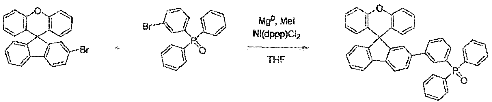
- this Grignard solution was cannulated to an anhydrous solution of (3-bromophenyl)dipheny!phosphine oxide (7.23 g, 1.0 eq., 20.3 mmol) and [ 1 ,3-bis(diphenylphosphino)propane]nickel(II) chloride (263 mg, 2.0 mol%, 0.49 mmol) in THF (200 mL). The resulting mixture was refluxed overnight after which it was quenched by addition of water (5 mL).
- the organic solvent was removed under reduced pressure, and the compound extracted with CHCI 3 (200 mL) and water ( 100 mL); the organic phase was decanted, further washed with water (2 x 200 mL), dried over MgS0 4 and evaporated to dryness.
- the crude product was filtered over silica; upon elution with n-hexane / DCM 2:1, apolar impurities was removed, while the desired was isolated using pure DCM, After removal of the DCM, the product was triturated in ethylacetate (100 mL), filtered off, and dried under vacuum yielding the title compound (7.5 g, 61%). Finally, the product was purified by sublimation (78% yield).
- this Grignard solution was cannulated to an anhydrous solution of (4-bromopheny!)diphenylphosphine oxide (7.23 g, 1.0 eq., 20.3 mmol) and [l ,3-bis(diphenylphosphino)propane]nickel(Il) chloride (263 mg, 2.0 mol%, 0.49 mmol) in THF (200 mL).
- the resulting mixture was refluxed overnight after which it was quenched by addition of water (5 mL).
- the organic solvent was removed under reduced pressure, and the compound extracted with DCM (2 L) and water (500 mL); the organic phase was decanted, dried over MgSC3 ⁇ 4 and evaporated to dryness.
- a first blue emitting device was made by depositing a 40 nm layer of HTM2 doped with PD2 (matrix to dopant weight ratio of 97:3 wt%) onto an ITO-glass substrate, followed by a 90 run undoped layer of HTML Subsequently, a blue fluorescent emitting layer of ABH113 (Sun Fine Chemicals) doped with NUBD370 (Sun Fine Chemicals) (97:3 wt%) was deposited with a thickness of 20 nm.
- ABH113 Un Fine Chemicals
- NUBD370 Un Fine Chemicals
- a 36 nm layer of the tested compound was deposited on the emitting layer together with the desired amount of the metallic element (usually, with 5 wt% Mg) as ETL, Subsequently, an aluminium layer with a thickness of 100 nm was deposited as a cathode.
- Example 2 A similar device was produced as in Example 1, with the difference that the emitter was omitted, and each combination matrix-dopant was tested in two different thicknesses of the ETL (40 and 80 nm) and with two different dopant concentrations (5 and 25 wt%).
- Example 1 A similar device was produced as in. Example 1 , with the difference that there were combined various compositions of semiconducting materials in the ETL with various emitter systems.
- Example 1 Al cathode was replaced with the sputtered indium tin oxide (ITO) cathode in combination with the Mg or Ba doped ETL.
- ITO indium tin oxide
- the results showed that ETLs based on divalent metal doped phosphine oxide matrices having redox potentials vs Fc+ Fc in the range from -2.24 V to -2,81 V are applicable also in top emitting OLEDs with cathode made of transparent semiconductive oxide.
- Comparative example 6 metal deposition using linear vaporization source
- 10 nm thick HTL consisting of 92 wt% auxiliary material F4 doped with 8 wt% PD2, 135 nm thick layer of neat F4, 25 nm thick blue emitting layer ABHl 13 (Sun Fine Chemicals) doped with NUBD370 (Sun Fine Chemicals) (97:3 wt%), 20 nm thick layer ABH036 (Sun Fine Chemicals), 10 nm thick CGL consisting of 95 wt% inventive compound E12 doped with 5 wt% Mg, 10 nm thick HTL consisting of 90 wt% auxiliary material F4 doped with 10 wt% PD2, 30 nm thick layer of neat F4, 15 nm thick layer of neat F3, 30 nm thick proprietary phosphorescent yellow emitting layer, 35 ran thick ETL of auxiliary material F5, 1 nm thick LiF layer and aluminium cathode.
- the diode operated at 6.81 V had EQE 24.4 %.
- the example 8 was repeated with Yb in the CGL instead of Mg.
- the diode operated at 6.80 V had EQE 23.9 %.
- the example 9 was repeated with compound E6 instead of El 2 in the CGL.
- the diode operated at 6.71 V had EQE 23.7 %.
- Comparative example 11 charge injection into adjacent or admixed high-LUMO ETM in a blue OLED
- HTL On the ITO substrate, 10 nm thick HTL consisting of 92 wt% auxiliary material F4 doped with 8 wt% PD2 followed by 130 nm thick layer of neat F4 were deposited by VIE. O top of the same emitting layer as in example 1, a 31 nm thick HBL of F6 and on top of it the doped ETL according to Table 5 were deposited subsequently, followed with the aluminium cathode. All deposition steps were done by VTE under pressure below 10 "2 Pa.
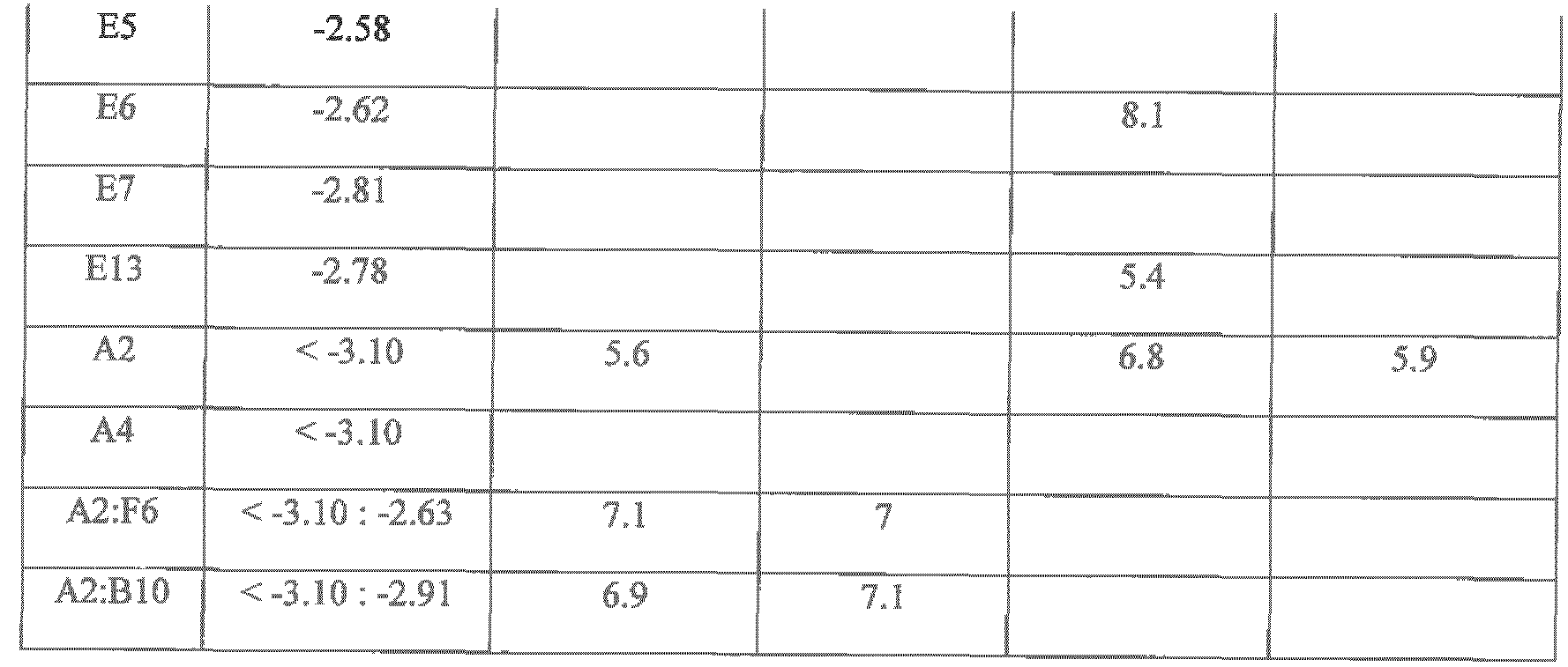
- A2 and A4 and their mixtures with ETMs which are fee of a polar group provided very good electron injection into adjacent F6 layer, despite its highly negative reduction potential. Due to highly negative reduction potential and low polarity of the F6 layer, the model device mimicks also the properties of devices comprising emitting layers made of light emitting polymers.
- Comparative example 12 charge injection into adjacent or admixed Mgh-LUMO ETM in a blue OLED
- Example 11 was repeated under replacement F6 in HBL with BIO. Composition of ETLs and results are shown in Table 6.
- Comparative example 13 (applicability of semiconducting materials based on phosphine oxide matrices doped with divalent metals in very thick ETLs)
- Example 11 was repeated with ETLs having thickness 150 nm. The results are shown in Table 7.
- Example 1 1 The device of Example 1 1 was reproduced with replacement of aluminium in the cathode with silver, compound CI as the electron, transport matrix and Mg as the electropositive element.
- Ag and Al cathode With Ag and Al cathode, the device operated at comparable voltages 4.0 and 3.9 V, but the quantum efficiency with Ag was 5.3 %, whereas with Al 4.9 %.
- the comparative device comprising as ETL compound CI doped with Dl operated with Al cathode at the voltage 4.7 V with quantum efficiency 3.3 %, and with Ag cathode at 5.7 V and quantum efficiency 2.5 %.
Landscapes
- Physics & Mathematics (AREA)
- Optics & Photonics (AREA)
- Engineering & Computer Science (AREA)
- Spectroscopy & Molecular Physics (AREA)
- Chemical & Material Sciences (AREA)
- Materials Engineering (AREA)
- Manufacturing & Machinery (AREA)
- Electroluminescent Light Sources (AREA)
Abstract
Description






Claims
Priority Applications (6)
| Application Number | Priority Date | Filing Date | Title |
|---|---|---|---|
| KR1020247011906A KR20240052092A (en) | 2015-06-23 | 2016-06-22 | Organic light emitting device comprising polar matrix, metal dopant and silver cathode |
| CN201680044669.8A CN107851733B (en) | 2015-06-23 | 2016-06-22 | Organic Light Emitting Device Containing Polar Host, Metal Dopant, and Silver Cathode |
| US15/738,672 US11355721B2 (en) | 2015-06-23 | 2016-06-22 | Organic light emitting device comprising polar matrix, metal dopant and silver cathode |
| KR1020187002068A KR20180019225A (en) | 2015-06-23 | 2016-06-22 | An organic light emitting device comprising a polar matrix, a metal dopant and a silver cathode |
| JP2017566731A JP2018518847A (en) | 2015-06-23 | 2016-06-22 | Organic light-emitting device comprising a polar matrix, a metal dopant and a silver cathode |
| CN202010630175.6A CN111900255B (en) | 2015-06-23 | 2016-06-22 | Organic light-emitting device containing polar matrix, metal dopant and silver cathode |
Applications Claiming Priority (2)
| Application Number | Priority Date | Filing Date | Title |
|---|---|---|---|
| EP15173443.1 | 2015-06-23 | ||
| EP15173443.1A EP3109916B1 (en) | 2015-06-23 | 2015-06-23 | Organic light emitting device comprising polar matrix, metal dopant and silver cathode |
Publications (1)
| Publication Number | Publication Date |
|---|---|
| WO2016207233A1 true WO2016207233A1 (en) | 2016-12-29 |
Family
ID=53496465
Family Applications (1)
| Application Number | Title | Priority Date | Filing Date |
|---|---|---|---|
| PCT/EP2016/064448 Ceased WO2016207233A1 (en) | 2015-06-23 | 2016-06-22 | Organic light emitting device comprising polar matrix, metal dopant and silver cathode |
Country Status (6)
| Country | Link |
|---|---|
| US (1) | US11355721B2 (en) |
| EP (1) | EP3109916B1 (en) |
| JP (2) | JP2018518847A (en) |
| KR (2) | KR20180019225A (en) |
| CN (2) | CN107851733B (en) |
| WO (1) | WO2016207233A1 (en) |
Families Citing this family (10)
| Publication number | Priority date | Publication date | Assignee | Title |
|---|---|---|---|---|
| DE102017111137B4 (en) * | 2017-05-22 | 2025-07-10 | Novaled Gmbh | Organic electroluminescent device |
| EP3425692B1 (en) * | 2017-07-07 | 2023-04-05 | Novaled GmbH | Organic electroluminescent device comprising an electron injection layer with zero-valent metal |
| EP3591725A1 (en) * | 2018-07-02 | 2020-01-08 | Novaled GmbH | Electronic device, method for preparing the same and a display device comprising the same |
| KR102290023B1 (en) * | 2018-11-06 | 2021-08-13 | 주식회사 엘지화학 | Organic light emitting device |
| EP3667755A1 (en) * | 2018-12-14 | 2020-06-17 | Novaled GmbH | Organic light emitting device, a method for manufacturing the same and a composition for use therein |
| KR20220072897A (en) * | 2020-11-24 | 2022-06-03 | 삼성디스플레이 주식회사 | light emitting device and electronic device including the light emitting device |
| US20240107876A1 (en) * | 2020-12-25 | 2024-03-28 | Idemitsu Kosan Co.,Ltd. | Organic electroluminescence device |
| KR102953090B1 (en) * | 2021-02-23 | 2026-04-15 | 삼성디스플레이 주식회사 | Light emitting device and electronic apparatus comprising the same |
| KR20230041845A (en) | 2021-09-16 | 2023-03-27 | 삼성디스플레이 주식회사 | Light emitting device and electronic apparatus including the same |
| WO2025033444A1 (en) * | 2023-08-08 | 2025-02-13 | パナソニックIpマネジメント株式会社 | Flame retardant and insulating material for wiring board |
Citations (3)
| Publication number | Priority date | Publication date | Assignee | Title |
|---|---|---|---|---|
| EP1486551A1 (en) * | 2003-06-13 | 2004-12-15 | Semiconductor Energy Laboratory Co., Ltd. | Electron injection composition for light emitting element, light emitting element and light emitting device |
| JP2006073581A (en) * | 2004-08-31 | 2006-03-16 | Toray Ind Inc | Light emitting device material and light emitting device |
| EP2452946A1 (en) * | 2010-11-16 | 2012-05-16 | Novaled AG | Pyridylphosphinoxides for organic electronic device and organic electronic device |
Family Cites Families (45)
| Publication number | Priority date | Publication date | Assignee | Title |
|---|---|---|---|---|
| US5093698A (en) | 1991-02-12 | 1992-03-03 | Kabushiki Kaisha Toshiba | Organic electroluminescent device |
| US5645948A (en) | 1996-08-20 | 1997-07-08 | Eastman Kodak Company | Blue organic electroluminescent devices |
| JPH10270171A (en) | 1997-01-27 | 1998-10-09 | Junji Kido | Organic electroluminescent device |
| JP4876333B2 (en) | 2000-06-08 | 2012-02-15 | 東レ株式会社 | Light emitting element |
| DE10058578C2 (en) | 2000-11-20 | 2002-11-28 | Univ Dresden Tech | Light-emitting component with organic layers |
| DE10116876B4 (en) | 2001-04-04 | 2004-09-23 | Infineon Technologies Ag | Process for doping electrically conductive organic compounds, organic field effect transistor and process for its production |
| KR100691543B1 (en) | 2002-01-18 | 2007-03-09 | 주식회사 엘지화학 | New material for electron transport and organic light emitting device using the same |
| JP3946106B2 (en) * | 2002-08-23 | 2007-07-18 | Hoya株式会社 | Mold for press and method for manufacturing lens |
| JP2004095221A (en) * | 2002-08-29 | 2004-03-25 | Toray Ind Inc | Light emitting element |
| US6703180B1 (en) * | 2003-04-16 | 2004-03-09 | Eastman Kodak Company | Forming an improved stability emissive layer from a donor element in an OLED device |
| DE102004010954A1 (en) | 2004-03-03 | 2005-10-06 | Novaled Gmbh | Use of a metal complex as an n-dopant for an organic semiconductive matrix material, organic semiconductor material and electronic component |
| US7507694B2 (en) | 2004-03-12 | 2009-03-24 | Halliburton Energy Services, Inc. | Surfactant-free emulsions and methods of use thereof |
| ES2394073T3 (en) * | 2004-03-26 | 2013-01-16 | Panasonic Corporation | Organic light emitting element |
| KR101027896B1 (en) | 2004-08-13 | 2011-04-07 | 테크니셰 유니베르시테트 드레스덴 | Layer Assembly for Luminescent Components |
| EP1648042B1 (en) | 2004-10-07 | 2007-05-02 | Novaled AG | A method for doping a semiconductor material with cesium |
| US20090324587A1 (en) | 2005-12-01 | 2009-12-31 | Neal Clifford Goodwin | Cancer Therapies and Pharmaceutical Compositions Used Therein |
| US20070126347A1 (en) * | 2005-12-01 | 2007-06-07 | Eastman Kodak Company | OLEDS with improved efficiency |
| DE502005004425D1 (en) | 2005-12-07 | 2008-07-24 | Novaled Ag | Method for depositing a vapor deposition material |
| DE602006001930D1 (en) | 2005-12-23 | 2008-09-04 | Novaled Ag | of organic layers |
| EP1804308B1 (en) | 2005-12-23 | 2012-04-04 | Novaled AG | An organic light emitting device with a plurality of organic electroluminescent units stacked upon each other |
| EP1837927A1 (en) | 2006-03-22 | 2007-09-26 | Novaled AG | Use of heterocyclic radicals for doping of organic semiconductors |
| AT502678B1 (en) | 2006-03-24 | 2007-05-15 | Alvatec Alkali Vacuum Technolo | Vaporizing source for gas phase generation comprising Bi alloy containing alkali and/or alkali earth metal useful in production of organic light emitting diodes doped with Na and in photocathode production |
| DE102007012794B3 (en) | 2007-03-16 | 2008-06-19 | Novaled Ag | Pyrido [3,2-h] quinazolines and / or their 5,6-dihydro derivatives, their method of preparation and doped organic semiconductor material containing them |
| US20080241518A1 (en) * | 2007-03-26 | 2008-10-02 | Tasuku Satou | Organic electroluminescence element |
| JP5230218B2 (en) * | 2007-03-26 | 2013-07-10 | ユー・ディー・シー アイルランド リミテッド | Organic electroluminescence device |
| JP2008244012A (en) | 2007-03-26 | 2008-10-09 | Fujifilm Corp | Organic electroluminescence device |
| JP2009076508A (en) | 2007-09-18 | 2009-04-09 | Fujifilm Corp | Organic electroluminescence device |
| DE102008011185A1 (en) | 2008-02-27 | 2009-09-03 | Osram Opto Semiconductors Gmbh | Process for producing a doped organic semiconducting layer |
| US8603642B2 (en) | 2009-05-13 | 2013-12-10 | Global Oled Technology Llc | Internal connector for organic electronic devices |
| JP5577186B2 (en) * | 2009-09-04 | 2014-08-20 | 株式会社ジャパンディスプレイ | Organic EL display device |
| FR2957718B1 (en) * | 2010-03-16 | 2012-04-20 | Commissariat Energie Atomique | HYBRID HIGH PERFORMANCE ELECTROLUMINESCENT DIODE |
| WO2011115738A2 (en) | 2010-03-17 | 2011-09-22 | Dean Lin | System and method for pedicle screw placement in vertebral alignment |
| EP2395571B1 (en) | 2010-06-10 | 2013-12-04 | Novaled AG | Organic electronic device comprising an organic semiconducting material |
| US8999530B2 (en) | 2011-06-13 | 2015-04-07 | Lg Chem, Ltd. | Compounds and organic electronic device using same |
| JP6170501B2 (en) | 2011-11-30 | 2017-07-26 | ノヴァレッド ゲーエムベーハー | display |
| KR102051360B1 (en) | 2011-11-30 | 2019-12-03 | 노발레드 게엠베하 | Organic electronic device |
| JP6165760B2 (en) | 2011-11-30 | 2017-07-19 | ノヴァレッド ゲーエムベーハー | Organic electronic equipment |
| JP6139552B2 (en) | 2011-12-06 | 2017-05-31 | ノヴァレッド ゲーエムベーハー | ORGANIC LIGHT-EMITTING ELEMENT AND MANUFACTURING METHOD |
| CN104321406B (en) | 2012-04-02 | 2017-06-16 | 诺瓦尔德股份有限公司 | Use of semiconductor compounds in organic light-emitting devices |
| DE102012217574A1 (en) * | 2012-09-27 | 2014-03-27 | Siemens Aktiengesellschaft | Phosphoroxo salts as n-dopants for organic electronics |
| EP2722908A1 (en) | 2012-10-17 | 2014-04-23 | Novaled AG | Phosphorescent OLED and hole transporting materials for phosphorescent OLEDs |
| JP2014103312A (en) * | 2012-11-21 | 2014-06-05 | Kobelco Kaken:Kk | Electrode for use in display device or input device, and sputtering gate for forming electrode |
| CN104037329A (en) | 2013-03-06 | 2014-09-10 | 海洋王照明科技股份有限公司 | Stacked organic light emitting device and preparation method thereof |
| EP3249714B1 (en) | 2013-04-10 | 2021-03-17 | Novaled GmbH | Semiconducting material comprising aza-substituted phosphine oxide matrix and metal salt |
| EP2860782B1 (en) | 2013-10-09 | 2019-04-17 | Novaled GmbH | Semiconducting material comprising a phosphine oxide matrix and metal salt |
-
2015
- 2015-06-23 EP EP15173443.1A patent/EP3109916B1/en active Active
-
2016
- 2016-06-22 JP JP2017566731A patent/JP2018518847A/en active Pending
- 2016-06-22 CN CN201680044669.8A patent/CN107851733B/en active Active
- 2016-06-22 CN CN202010630175.6A patent/CN111900255B/en active Active
- 2016-06-22 WO PCT/EP2016/064448 patent/WO2016207233A1/en not_active Ceased
- 2016-06-22 US US15/738,672 patent/US11355721B2/en active Active
- 2016-06-22 KR KR1020187002068A patent/KR20180019225A/en not_active Ceased
- 2016-06-22 KR KR1020247011906A patent/KR20240052092A/en not_active Ceased
-
2021
- 2021-05-06 JP JP2021078763A patent/JP7503521B2/en active Active
Patent Citations (3)
| Publication number | Priority date | Publication date | Assignee | Title |
|---|---|---|---|---|
| EP1486551A1 (en) * | 2003-06-13 | 2004-12-15 | Semiconductor Energy Laboratory Co., Ltd. | Electron injection composition for light emitting element, light emitting element and light emitting device |
| JP2006073581A (en) * | 2004-08-31 | 2006-03-16 | Toray Ind Inc | Light emitting device material and light emitting device |
| EP2452946A1 (en) * | 2010-11-16 | 2012-05-16 | Novaled AG | Pyridylphosphinoxides for organic electronic device and organic electronic device |
Also Published As
| Publication number | Publication date |
|---|---|
| JP2021119637A (en) | 2021-08-12 |
| US20180190922A1 (en) | 2018-07-05 |
| EP3109916A1 (en) | 2016-12-28 |
| CN111900255A (en) | 2020-11-06 |
| CN107851733B (en) | 2020-07-17 |
| KR20240052092A (en) | 2024-04-22 |
| US11355721B2 (en) | 2022-06-07 |
| CN111900255B (en) | 2024-03-15 |
| JP2018518847A (en) | 2018-07-12 |
| KR20180019225A (en) | 2018-02-23 |
| JP7503521B2 (en) | 2024-06-20 |
| EP3109916B1 (en) | 2021-08-25 |
| CN107851733A (en) | 2018-03-27 |
Similar Documents
| Publication | Publication Date | Title |
|---|---|---|
| US20240298524A1 (en) | N-Doped Semiconducting Material Comprising Phosphine Oxide Matrix and Metal Dopant | |
| JP7443286B2 (en) | Organic light emitting devices containing polar matrices and metal dopants | |
| JP7503521B2 (en) | Organic light-emitting device including a polar matrix, a metal dopant, and a silver cathode | |
| EP3109915B1 (en) | Organic light emitting device comprising polar matrix and metal dopant | |
| EP3168886A1 (en) | Metallic layer comprising alkali metal and second metal | |
| EP3109919B1 (en) | N-doped semiconducting material comprising polar matrix and metal dopant | |
| HK1212095B (en) | N-doped semiconducting material comprising phosphine oxide matrix and metal dopant |
Legal Events
| Date | Code | Title | Description |
|---|---|---|---|
| 121 | Ep: the epo has been informed by wipo that ep was designated in this application |
Ref document number: 16733384 Country of ref document: EP Kind code of ref document: A1 |
|
| ENP | Entry into the national phase |
Ref document number: 2017566731 Country of ref document: JP Kind code of ref document: A |
|
| NENP | Non-entry into the national phase |
Ref country code: DE |
|
| ENP | Entry into the national phase |
Ref document number: 20187002068 Country of ref document: KR Kind code of ref document: A |
|
| 122 | Ep: pct application non-entry in european phase |
Ref document number: 16733384 Country of ref document: EP Kind code of ref document: A1 |
|
| WWR | Wipo information: refused in national office |
Ref document number: 1020247011906 Country of ref document: KR |