WO2016194655A1 - 信号処理装置および方法 - Google Patents
信号処理装置および方法 Download PDFInfo
- Publication number
- WO2016194655A1 WO2016194655A1 PCT/JP2016/065025 JP2016065025W WO2016194655A1 WO 2016194655 A1 WO2016194655 A1 WO 2016194655A1 JP 2016065025 W JP2016065025 W JP 2016065025W WO 2016194655 A1 WO2016194655 A1 WO 2016194655A1
- Authority
- WO
- WIPO (PCT)
- Prior art keywords
- rtc
- time
- chip
- power supply
- signal
- Prior art date
- Legal status (The legal status is an assumption and is not a legal conclusion. Google has not performed a legal analysis and makes no representation as to the accuracy of the status listed.)
- Ceased
Links
Images





Classifications
-
- G—PHYSICS
- G06—COMPUTING OR CALCULATING; COUNTING
- G06F—ELECTRIC DIGITAL DATA PROCESSING
- G06F1/00—Details not covered by groups G06F3/00 - G06F13/00 and G06F21/00
- G06F1/04—Generating or distributing clock signals or signals derived directly therefrom
- G06F1/12—Synchronisation of different clock signals provided by a plurality of clock generators
-
- G—PHYSICS
- G04—HOROLOGY
- G04G—ELECTRONIC TIME-PIECES
- G04G3/00—Producing timing pulses
-
- G—PHYSICS
- G04—HOROLOGY
- G04G—ELECTRONIC TIME-PIECES
- G04G7/00—Synchronisation
-
- G—PHYSICS
- G06—COMPUTING OR CALCULATING; COUNTING
- G06F—ELECTRIC DIGITAL DATA PROCESSING
- G06F1/00—Details not covered by groups G06F3/00 - G06F13/00 and G06F21/00
- G06F1/04—Generating or distributing clock signals or signals derived directly therefrom
- G06F1/14—Time supervision arrangements, e.g. real time clock
-
- G—PHYSICS
- G06—COMPUTING OR CALCULATING; COUNTING
- G06F—ELECTRIC DIGITAL DATA PROCESSING
- G06F1/00—Details not covered by groups G06F3/00 - G06F13/00 and G06F21/00
- G06F1/26—Power supply means, e.g. regulation thereof
- G06F1/32—Means for saving power
- G06F1/3203—Power management, i.e. event-based initiation of a power-saving mode
- G06F1/3206—Monitoring of events, devices or parameters that trigger a change in power modality
-
- G—PHYSICS
- G06—COMPUTING OR CALCULATING; COUNTING
- G06F—ELECTRIC DIGITAL DATA PROCESSING
- G06F1/00—Details not covered by groups G06F3/00 - G06F13/00 and G06F21/00
- G06F1/26—Power supply means, e.g. regulation thereof
- G06F1/32—Means for saving power
- G06F1/3203—Power management, i.e. event-based initiation of a power-saving mode
- G06F1/3234—Power saving characterised by the action undertaken
- G06F1/3287—Power saving characterised by the action undertaken by switching off individual functional units in the computer system
-
- Y—GENERAL TAGGING OF NEW TECHNOLOGICAL DEVELOPMENTS; GENERAL TAGGING OF CROSS-SECTIONAL TECHNOLOGIES SPANNING OVER SEVERAL SECTIONS OF THE IPC; TECHNICAL SUBJECTS COVERED BY FORMER USPC CROSS-REFERENCE ART COLLECTIONS [XRACs] AND DIGESTS
- Y02—TECHNOLOGIES OR APPLICATIONS FOR MITIGATION OR ADAPTATION AGAINST CLIMATE CHANGE
- Y02D—CLIMATE CHANGE MITIGATION TECHNOLOGIES IN INFORMATION AND COMMUNICATION TECHNOLOGIES [ICT], I.E. INFORMATION AND COMMUNICATION TECHNOLOGIES AIMING AT THE REDUCTION OF THEIR OWN ENERGY USE
- Y02D10/00—Energy efficient computing, e.g. low power processors, power management or thermal management
Definitions
- the present disclosure relates to a signal processing apparatus and method, and more particularly, to a signal processing apparatus and method that can perform synchronization while maintaining high resolution even when the resolution of the RTC is different.
- the real-time clock (hereinafter referred to as RTC) has a power supply that is independent of the main function in the chip, and when the main power supply is stopped to reduce power consumption. Is used when it is desired to use continuous time information (see Patent Document 1).
- CMOS Complementary Metal Oxide Semiconductor
- the present disclosure has been made in view of such a situation, and even when the resolution of the RTC is different, synchronization can be performed while maintaining high resolution.
- a signal processing device includes a first RTC (real time clock) that holds time by a count operation based on a clock signal, the first chip that performs operation control, and the first RTC.
- a second chip having a different second RTC and performing power supply control, wherein the first chip synchronizes the time of the first RTC and the time of the second RTC.
- the operation control unit can synchronize the time of the second RTC with the first RTC when the first chip recovers from the power stop.
- the operation control unit is time information that can be held only by the first RTC before the power supply of the first chip is stopped. Can be held in the memory as difference information between the times of the first RTC and the second RTC, and used when the first chip is restored from power-off.
- the operation control unit can synchronize the time of the first RTC with the second RTC when updating the time information of the first RTC.
- a signal processing method includes a first RTC that holds time by a count operation based on a clock signal, a first chip that performs operation control, and a second RTC that is different from the first RTC.
- a signal processing device including a second chip having an RTC and performing power supply control synchronizes the time of the first RTC and the time of the second RTC.
- the time of the first RTC included in the first chip that performs operation control, and the second RTC included in the second chip that performs power supply control which is different from the first RTC.
- the time is synchronized.
- multiple RTCs can be synchronized.
- a plurality of RTCs can be synchronized while maintaining a high resolution.
- GPS Global Positioning System
- the real-time clock (hereinafter referred to as RTC) has a power supply that is independent of the main function in the chip, and when the main power supply is stopped to reduce power consumption. Used when you want to use continuous time information.
- CMOS Complementary Metal Oxide Semiconductor
- the clock input to Do RTC small resolution, in the A of FIG. 1, is 1/2 6 divided in the RTC, examples being input to the counter is shown Has been.
- the place to be divided may be anywhere in the chip before being input to the counter.
- the frequency division is the same.
- ephemeris and almanac can be used, and when performing hot start using these, time information at the bit boundary of 50 bps data from each satellite to be received is used, and in 20 ms of the same data section Perform correlation integration.
- time information at the bit boundary is shifted by ⁇ t (ms)
- the added value 2 ⁇ t is canceled out and the integrated value is reduced, resulting in deterioration of sensitivity.
- the correlation value deteriorates by 10 Log ((20 ⁇ 2 ⁇ t) / 20) dB. For this reason, it is required to have an RTC with sufficiently high resolution.
- the resolution of the external RTC is the resolution of the RTC of the GPS receiver.
- the time information at the bit boundary is shifted by the difference in resolution, causing sensitivity deterioration.
- ⁇ t ⁇ 0.5ms
- sensitivity degradation of 0.22dB occurs.
- ⁇ t ⁇ 1 ms
- sensitivity degradation of 0.46 dB occurs.
- each has an independent RTC, and these are synchronized with each other.
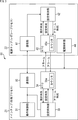
- FIG. 3 is a block diagram illustrating a configuration example of a signal processing device to which the present technology is applied.
- the signal processing apparatus 11 is configured to include a main chip 21 for advanced processes and a power supply chip 22 for legacy processes.
- the main chip 21 includes an operation control unit 31, a communication unit 32, a setting holding unit 33, and an RTC 34 having a counter.
- the power supply chip 22 includes a communication unit 41, a setting holding unit 42, an RTC 43 having a counter 43a, and a power supply control unit 44.
- the operation control unit 31 controls the operation of each unit of the signal processing device 11. That is, the operation control unit 31 controls the operation of each unit of the main chip 21 and each unit of the power supply chip 22.
- the communication unit 32 communicates with the communication unit 32 of the power supply chip 22 under the control of the operation control unit 31.
- the setting holding unit 33 holds time information (set time and alarm time) under the control of the operation control unit 31.
- the RTC 34 holds the time by the counting operation of the counter 34a based on the RTC clock signal from the outside.
- the communication unit 41 communicates with the communication unit 41 of the main chip 21 under the control of the operation control unit 31.
- the setting holding unit 42 holds time information (set time and alarm time) under the control of the operation control unit 31.
- the RTC 43 holds the time by the counting operation of the counter 43a by the RTC clock signal from the outside.
- the power control unit 44 controls the power supply to the main chip 21 under the control of the operation control unit 31.
- the counter value of the RTC 34 is also cleared, so that it is difficult for the RTC 34 to keep a continuous time before and after the stop. Therefore, in the signal processing device 11, the RTC 34 of the main chip 21 and the RTC 43 of the power supply chip 22 are synchronized before the power supply of the main chip 21 is stopped, and after the power supply of the main chip 21 is restored, the RTC 34 and the power supply of the main chip 21 again. The RTC 43 of the chip 22 is synchronized. By doing so, the RTC 34 can handle continuous time information before and after the stop.
- the proportion of power consumed by leakage current has increased due to the miniaturization of the CMOS process.
- the power supply of the main chip 21 including the power supply of the RTC 34 can be completely stopped by this technology. The power consumption can be reduced.
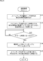
- step S11 the main chip 21 reads the current time of the RTC 43 of the power supply chip 22. That is, the RTC 43 reads the current time held by the counter 43a under the control of the operation control unit 31 as indicated by an arrow A11 in FIG. 5, and the read current time is set to the setting holding unit 42 and the communication unit 41. And the operation control unit 31 via the communication unit 32.
- step S12 the main chip 21 informs the power supply chip 22 of a time that is later than the current time of the read counter 43a, and causes the setting holding unit 33 to hold the set time.
- the setting holding unit 33 holds a future time as a set time.
- the RTC 43 of the power supply chip 22 receives the future time from the main chip 21 via the communication unit 41 and the setting holding unit 42 and supplies it to the counter 43a of the RTC 43 as an alarm time, as indicated by an arrow A12 in FIG. To do.
- step S13 the RTC 43 of the power supply chip 22 compares the alarm time with the current time of the counter 43a and waits until it is determined that the alarm time has come. If it is determined in step S13 that the alarm time has come, the process proceeds to step S14.
- step S14 the RTC 43 of the power supply chip 22 raises an alarm to the RTC 34 as indicated by an arrow A12 in FIG.
- step S15 the RTC 34 starts the counter 34a of the RTC 34 from the set time held in the setting holding unit 33 when receiving an alarm as indicated by an arrow A13 in FIG.
- the time of the RTC 43 of the power supply chip 22 can be synchronized with the RTC 34 of the main chip 21.
- the RTC 34 may require high resolution. Even when the resolution of the RTC 34 of the main chip 21 is higher than the resolution of the RTC 43 of the power supply chip 22, in order to maintain the resolution of the main chip and synchronize the RTC time of the power supply chip with the RTC of the main chip, the main chip 21 has the non-volatile storage unit 61 shown in FIG. 6.
- the main chip 21 and the power supply chip 22 are synchronized as follows in a state where both are generated.
- the RTC 34 is provided with a register 71
- the RTC 43 is provided with a comparator 81 and an alarm setting register 82. 33
- the alarm setting register 82 is generally provided in the setting holding unit 42.
- the main chip 21 reads the current time of the RTC 43 of the power supply chip 22 in the same manner as the processing in step S11 in FIG.
- the chip 21 informs the power supply chip 22 of a time later than the current time of the read counter 43a, and causes the setting holding unit 33 to hold it as the set time.
- the setting holding unit 33 stores the set time in the register b of the register 71.
- the RTC 43 of the power supply chip 22 is transmitted from the main chip 21 as in the processing of steps S13 and S14.
- the alarm time held in the setting holding unit 42 (actually set in the alarm setting register 82) matches the current time counted in the counter 43a of the RTC 43 by the comparison of the comparator 81, the RTC 43 Raises an alarm to the RTC 34 as indicated by arrow A21.
- the main chip 21 loads the set time stored in the register b of the register 71 into the MSB of the counter as indicated by an arrow A22.
- the main chip 21 uses a resolution count value (LSB: 6 bits) which the counter 34a of the RTC 34 of the power supply chip 22 does not have, as indicated by an arrow A23, and the register b of the register 71 and the nonvolatile storage unit. 61.
- the main chip 21 and the power supply chip 22 are synchronized when both are in a state of occurrence.
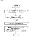
- step S31 the main chip 21 informs the power supply chip 22 of a future time rather than the current time of its own RTC 34. That is, as indicated by the arrow A31, the RTC 34 of the main chip 21 supplies the current time counted by the counter 34a to the operation control unit 31 via the setting holding unit 33 under the control of the operation control unit 31. To do.
- the operation control unit 31 notifies the setting holding unit 42 of a future time rather than the current time of the RTC 34 via the communication unit 32 and the communication unit 41 of the power supply chip 22.
- the setting holding unit 42 holds this future time as the setting time. At this time, the operation control unit 31 transmits this future time to the RTC 34 via the setting holding unit 33 as an alarm time.
- step S32 the RTC 34 compares the alarm time with the current time of the counter 34a and waits until it is determined that the time (alarm time) has come. If it is determined in step S32 that the time has come, the process proceeds to step S33.
- step S33 the RTC 34 raises an alarm to the RTC 43 of the power supply chip 22 as indicated by an arrow A32.
- step S34 the power supply chip 22 receives an alarm from the main chip 21, and sets the set time (future time) previously transmitted from the main chip 21 to the counter 43a of its own RTC 43. That is, the setting holding unit 42 supplies the held setting time to the RTC 43 as indicated by an arrow A33. The RTC 43 sets the set time in the counter 43a.
- the time of the RTC 34 of the main chip 21 can be synchronized with the RTC 43 of the power supply chip 22.
- the RTC time of each chip can be synchronized in both directions.
- synchronization can be performed while maintaining a high resolution.
- the entire main chip can be powered off to enable low power consumption operation.
- the signal processing apparatus has been described as an example, but the present technology can also be applied to the following GPS module.
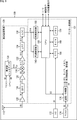
- FIG. 9 is a block diagram illustrating a configuration example of a GPS module to which the present technology is applied.
- the GPS module 100 includes an antenna 112, a frequency conversion unit 120, a synchronization acquisition unit 140, a synchronization holding unit 150, a CPU (Central Processing Unit) 160, an RTC (Real Time Clock) 164, a timer 168, and a memory. 170, an XO (crystal oscillator, x'tal Oscillator) 172, a TCXO (Temperature Compensated X'tal Oscillator) 174, and a multiplier / divider 176.
- XO crystal oscillator, x'tal Oscillator
- TCXO Tempoture Compensated X'tal Oscillator
- the XO 172 oscillates a signal D1 having a predetermined frequency (for example, about 32.768 kHz) and supplies the oscillated signal D1 to the RTC 164.
- the TCXO 174 oscillates a signal D2 having a frequency (for example, about 16.368 MHz) different from that of the XO 172, and supplies the oscillated signal D2 to the multiplier / divider 76 and the frequency synthesizer 128.
- the multiplier / divider 176 multiplies and / or divides the signal D2 supplied from the TCXO 174 based on an instruction from the CPU 160. Then, the multiplier / divider 176 performs the frequency synthesizer 128, the ADC 136, the CPU 160, the timer 160, the memory 170, the synchronization acquisition unit 140, and the synchronization of the signal D4 that has been multiplied and / or divided. Supply to holding unit 150.
- the antenna 112 receives a radio signal including a navigation message transmitted from a GPS satellite which is a satellite of the global positioning system (for example, an RF signal in which a carrier of 1557.42 MHz is spread), and the radio signal is converted into an electric signal D5. And is supplied to the frequency converter 120.
- a GPS satellite which is a satellite of the global positioning system (for example, an RF signal in which a carrier of 1557.42 MHz is spread)
- the radio signal is converted into an electric signal D5. And is supplied to the frequency converter 120.
- the frequency converter 120 includes an LNA (Low Noise Amplifier) 122, a BPF (Band Pass Filter) 124, an amplifier 126, a frequency synthesizer 128, a multiplier 130, an amplifier 132, an LPF (Low Pass Filter) 134, and an ADC (Analog Digital Converter). ) 136.
- the frequency conversion unit 120 converts a signal D5 having a high frequency of 1575.42 MHz received by the antenna 112 into a signal D14 having a frequency of, for example, about 1.023 MHz in order to facilitate digital signal processing. Down-convert to.
- the LNA 122 amplifies the signal D5 supplied from the antenna 112 and supplies it to the BPF 124.
- the BPF 124 is composed of a SAW filter (Surface Acoustic Wave Filter), and extracts only a specific frequency component from the frequency components of the signal D6 amplified by the LNA 122 and supplies it to the amplifier 126.
- the amplifier 126 amplifies the signal D7 (frequency FRF) having the frequency component extracted by the BPF 124, and supplies the amplified signal D7 to the multiplier 130.
- the frequency synthesizer 128 uses the signal D2 supplied from the TCXO 174 and generates a signal D10 having a frequency FLO based on an instruction D9 from the CPU 160. Then, the frequency synthesizer 128 supplies the signal D10 having the generated frequency FLO to the multiplier 130.
- Multiplier 130 multiplies signal D 8 having frequency FRF supplied from amplifier 126 and signal D 10 having frequency FLO supplied from frequency synthesizer 128. That is, the multiplier 130 down-converts the high-frequency signal into an IF (Intermediate Frequency) signal D11 (for example, an intermediate frequency signal having a frequency of about 1.023 MHz).
- IF Intermediate Frequency
- the amplifier 132 amplifies the IF signal D11 down-converted by the multiplier 130 and supplies it to the LPF 134.
- the LPF 134 extracts a low frequency component from the frequency components of the IF signal D12 amplified by the amplifier 130, and supplies a signal D13 having the extracted low frequency component to the ADC 136.
- FIG. 9 illustrates an example in which the LPF 134 is disposed between the amplifier 132 and the ADC 136, a BPF may be disposed between the amplifier 132 and the ADC 136.
- the ADC 136 samples the analog IF signal D13 supplied from the LPF 134 to convert it into a digital format, and supplies the IF signal D14 converted into the digital format to the synchronization capturing unit 140 and the synchronization holding unit 150 bit by bit. .
- the synchronization acquisition unit 140 uses the signal D3 supplied from the multiplier / divider 176 based on the control by the CPU 160 and uses a pseudo-random (PRN) code of the IF signal D14 supplied from the ADC 136. Perform synchronization acquisition. Further, the synchronization acquisition unit 140 detects the carrier frequency of the IF signal D14. Then, the synchronization acquisition unit 140 supplies the phase of the PRN code, the carrier frequency of the IF signal D14, and the like to the synchronization holding unit 150 and the CPU 160.
- PRN pseudo-random
- the synchronization holding unit 150 uses the signal D3 supplied from the multiplier / divider 176 based on control by the CPU 160 to hold the synchronization of the PRN code of the IF signal D14 supplied from the ADC 136 and the carrier. More specifically, the synchronization holding unit 150 operates using the phase of the PRN code supplied from the synchronization acquisition unit 140 and the carrier frequency of the IF signal D14 as initial values. Then, the synchronization holding unit 150 demodulates the navigation message included in the IF signal D14 supplied from the ADC 136, and supplies the demodulated navigation message, the phase of the highly accurate PRN code, and the carrier frequency to the CPU 160.
- the CPU 160 calculates the position and velocity of each GPS satellite based on the navigation message supplied from the synchronization holding unit 150, the phase of the PRN code, and the carrier frequency, and calculates the position of the GPS module 100. Further, the CPU 160 may correct the time information of the RTC 164 based on the navigation message. Further, the CPU 160 may be connected to a control terminal, an I / O terminal, an additional function terminal, and the like, and execute other various control processes.
- the RTC 164 measures time using a signal D1 having a predetermined frequency supplied from the XO 172. The time measured by the RTC 164 is appropriately corrected by the CPU 160.
- Timer 168 counts using signal D4 supplied from multiplier / divider 176.
- the timer 168 is referred to when determining the start timing of various controls by the CPU 160.
- the CPU 160 refers to the timer 168 when determining the timing for starting the operation of the PRN code generator of the synchronization holding unit 150 based on the phase of the PRN code captured by the synchronization capturing unit 140.
- the memory 170 includes a RAM (Random Access Memory), a ROM (Read-Only Memory), and the like, and has functions as a work space by the CPU 160, a program storage unit, a navigation message storage unit, and the like.
- a RAM is used as a work area when performing various processes by the CPU 160 or the like.
- the RAM also holds buffering of various input data, ephemeris and almanac which are GPS satellite orbit information obtained from the synchronization holding unit 150, and intermediate data or calculation result data generated in the calculation process. It can also be used for such as.
- a ROM is used as means for storing various programs, fixed data, and the like.
- the memory 170 while the GPS module 100 is turned off, the ephemeris and almanac which are the orbit information of the GPS satellite, the position information of the positioning result, the error amount of the TCXO1, and the like are stored as nonvolatile. Memory may be used.
- each block excluding XO 172, TCXO 174, antenna 112 and BPF 124 can be mounted on an integrated circuit consisting of one chip.
- the above-described synchronization acquisition unit 140 uses a matched filter in order to perform synchronization acquisition of a spread code at high speed, for example.
- the synchronization acquisition unit 140 may use a transversal filter as a matched filter.
- the synchronization acquisition unit 140 may use a digital matched filter that uses a fast Fourier transform (FFT) as a matched filter.
- FFT fast Fourier transform
- Such a digital matched filter may be implemented as software executed using a DSP (Digital Signal Processor).
- the unit 121 includes a plurality of chips, that is, the main chip 21 and the power supply chip 22 as described above.
- the CPU 160 corresponds to the operation control unit 31 of the main chip 21
- the RTC 164 corresponds to the RTC 34 of the main chip 21 and the RTC 43 of the power supply chip 22
- the memory 170 corresponds to the setting holding unit 33 of the main chip 21. This corresponds to the setting holding unit 42 of the power supply chip 22.
- the I / O terminal corresponds to the communication unit 32 and the communication unit 41.
- the effect similar to this technique can be acquired. That is, when the RTC resolution is different, which is composed of a plurality of chips, synchronization can be performed while maintaining high resolution, and low power consumption can be achieved.
- the series of processes described above can be executed by hardware or software.
- a program constituting the software is installed from a network or a recording medium.
- this recording medium is constituted by a removable medium on which the program is recorded, which is distributed to distribute the program to the user, separately from the apparatus main body.
- the removable media includes magnetic disks (including flexible disks) and optical disks (including CD-ROMs and DVDs). Further, magneto-optical disks (including MD (Mini-Disc)) and semiconductor memories are also included.
- the program can be installed in the storage unit via the input / output interface by attaching the removable media to the drive.
- This program can also be provided via a wired or wireless transmission medium such as a local area network, the Internet, or digital satellite broadcasting.
- the program can be installed in the communication unit (for example, I / O) of each device.
- this program can be installed in advance in the ROM or storage unit (for example, the memory 170) of each device.
- the program executed by the computer may be a program that is processed in time series in the order described in this specification, or in parallel or at a necessary timing such as when a call is made. It may be a program for processing.
- system means an overall device configured by a plurality of devices, blocks, means, and the like.
- the configuration described as one device (or processing unit) may be divided and configured as a plurality of devices (or processing units).
- the configurations described above as a plurality of devices (or processing units) may be combined into a single device (or processing unit).
- a configuration other than that described above may be added to the configuration of each device (or each processing unit).
- a part of the configuration of a certain device (or processing unit) may be included in the configuration of another device (or other processing unit). . That is, the present technology is not limited to the above-described embodiment, and various modifications can be made without departing from the gist of the present technology.
- this technique can also take the following structures.
- a first chip that has a first RTC (real-time clock) that holds time in a counting operation by a clock signal and performs operation control;
- a second chip having a second RTC different from the first RTC and performing power supply control,
- the first chip includes an operation control unit that synchronizes the time of the first RTC and the time of the second RTC.
- the signal processing device wherein the operation control unit synchronizes the time of the second RTC with the first RTC when the first chip returns from a power stop.
- the operation control unit can hold only the first RTC before the power supply of the first chip is stopped.
- Time information is stored in a memory as difference information between the time of the first RTC and the time of the second RTC, and used when the first chip is returned from power shutdown.
- the signal processing according to (2) apparatus (4)
- the operation control unit can hold only the first RTC before the power supply of the first chip is stopped.
- Time information is stored in the memory as difference information between the time of the first RTC and the time of the second RTC, and is used when the first chip is returned from power stoppage.
- a signal processing apparatus comprising: a second chip having a second RTC different from the first RTC and performing power supply control; A signal processing method for synchronizing the time of the first RTC and the time of the second RTC.
- 11 signal processing device 21 main chip, 22 power supply chip, 31 operation control unit, 32 communication unit, 33 setting holding unit, 34 RTC, 34a counter, 41 communication unit, 42 setting holding unit 43 RTC, 43a counter, 44 power holding Part, 61 non-volatile memory, 71 register, 81 comparator, 82 alarm setting register, 100 GPS system, 120 frequency conversion part, 121 digital circuit part, 160 CPU, RTC 164, 170 memory
Landscapes
- Engineering & Computer Science (AREA)
- Theoretical Computer Science (AREA)
- Physics & Mathematics (AREA)
- General Physics & Mathematics (AREA)
- General Engineering & Computer Science (AREA)
- Computer Hardware Design (AREA)
- Computing Systems (AREA)
- Electric Clocks (AREA)
- Power Sources (AREA)
Abstract
Description
一般的にリアルタイムクロック(以下、RTC)は、チップ内で、メインの機能とは独立した電源を有し、メインの電源を停止させて低消費電力化を図る場合で、電源復帰後にも停止前と連続した時刻情報を使用したいときに使用される。
図3は、本技術を適用した信号処理装置の構成例を示すブロック図である。
次に、図4のフローチャートと図5を参照して、信号処理装置11の信号処理としての同期処理について説明する。
次に、図7のフローチャートと図8を参照して、信号処理装置11の信号処理としての同期処理の他の例について説明する。例えば、GPS受信機において、高精度の時刻情報を取得するメインチップ21の機能があり、RTC34の時刻情報が更新され、その時刻情報に、RTC43を同期させる場合の例について説明する。
図9は、本技術を適用したGPSモジュールの構成例を示すブロック図である。
(1) クロック信号によるカウント動作で時刻を保持する第1のRTC(リアルタイムクロック)を有し、動作制御を行う第1のチップと、
前記第1のRTCとは異なる第2のRTCを有し、電源制御を行う第2のチップと
を備え、
前記第1のチップは、前記第1のRTCの時刻と、前記第2のRTCの時刻とを同期させる動作制御部を有する
信号処理装置。
(2) 前記動作制御部は、前記第1のチップの電源停止からの復帰時に、前記第2のRTCの時刻を、前記第1のRTCに同期させる
前記(1)に記載の信号処理装置。
(3) 前記動作制御部は、前記第1のRTCの分解能が、前記第2のRTCの分解能よりも高い場合、前記第1のチップの電源停止前に、前記第1のRTCのみが保持可能な時刻情報を、前記第1のRTCと前記第2のRTCの時刻の差分情報としてメモリに保持させ、前記第1のチップの電源停止からの復帰時に使用させる
前記(2)に記載の信号処理装置。
(4) 前記動作制御部は、前記第1のRTCの分解能が、前記第2のRTCの分解能よりも高い場合、前記第1のチップの電源停止前に、前記第1のRTCのみが保持可能な時刻情報を、前記第1のRTCと前記第2のRTCの時刻の差分情報としてメモリに保持させ、前記第1のチップの電源停止からの復帰時に使用させる
前記(1)乃至(3)のいずれかに記載の信号処理装置。
(5) クロック信号によるカウント動作で時刻を保持する第1のRTCを有し、動作制御を行う第1のチップと、
前記第1のRTCとは異なる第2のRTCを有し、電源制御を行う第2のチップと
を備える信号処理装置が、
前記第1のRTCの時刻と、前記第2のRTCの時刻とを同期させる
信号処理方法。
Claims (5)
- クロック信号によるカウント動作で時刻を保持する第1のRTC(リアルタイムクロック)を有し、動作制御を行う第1のチップと、
前記第1のRTCとは異なる第2のRTCを有し、電源制御を行う第2のチップと
を備え、
前記第1のチップは、前記第1のRTCの時刻と、前記第2のRTCの時刻とを同期させる動作制御部を有する
信号処理装置。 - 前記動作制御部は、前記第1のチップの電源停止からの復帰時に、前記第2のRTCの時刻を、前記第1のRTCに同期させる
請求項1に記載の信号処理装置。 - 前記動作制御部は、前記第1のRTCの分解能が、前記第2のRTCの分解能よりも高い場合、前記第1のチップの電源停止前に、前記第1のRTCのみが保持可能な時刻情報を、前記第1のRTCと前記第2のRTCの時刻の差分情報としてメモリに保持させ、前記第1のチップの電源停止からの復帰時に使用させる
請求項2に記載の信号処理装置。 - 前記動作制御部は、前記第1のRTCの分解能が、前記第2のRTCの分解能よりも高い場合、前記第1のチップの電源停止前に、前記第1のRTCのみが保持可能な時刻情報を、前記第1のRTCと前記第2のRTCの時刻の差分情報としてメモリに保持させ、前記第1のチップの電源停止からの復帰時に使用させる
請求項1に記載の信号処理装置。 - クロック信号によるカウント動作で時刻を保持する第1のRTC(リアルタイムクロック)を有し、動作制御を行う第1のチップと、
前記第1のRTCとは異なる第2のRTCを有し、電源制御を行う第2のチップと
を備える信号処理装置が、
前記第1のRTCの時刻と、前記第2のRTCの時刻とを同期させる
信号処理方法。
Priority Applications (2)
| Application Number | Priority Date | Filing Date | Title |
|---|---|---|---|
| US15/577,183 US10591953B2 (en) | 2015-06-05 | 2016-05-20 | Signal processing apparatus and method |
| JP2017521815A JP6786482B2 (ja) | 2015-06-05 | 2016-05-20 | 信号処理装置および方法 |
Applications Claiming Priority (2)
| Application Number | Priority Date | Filing Date | Title |
|---|---|---|---|
| JP2015-114911 | 2015-06-05 | ||
| JP2015114911 | 2015-06-05 |
Publications (1)
| Publication Number | Publication Date |
|---|---|
| WO2016194655A1 true WO2016194655A1 (ja) | 2016-12-08 |
Family
ID=57441263
Family Applications (1)
| Application Number | Title | Priority Date | Filing Date |
|---|---|---|---|
| PCT/JP2016/065025 Ceased WO2016194655A1 (ja) | 2015-06-05 | 2016-05-20 | 信号処理装置および方法 |
Country Status (3)
| Country | Link |
|---|---|
| US (1) | US10591953B2 (ja) |
| JP (1) | JP6786482B2 (ja) |
| WO (1) | WO2016194655A1 (ja) |
Cited By (2)
| Publication number | Priority date | Publication date | Assignee | Title |
|---|---|---|---|---|
| JP2018159644A (ja) * | 2017-03-23 | 2018-10-11 | カシオ計算機株式会社 | 時計装置、時刻補正方法及びプログラム |
| CN110967967A (zh) * | 2018-09-28 | 2020-04-07 | 三星电子株式会社 | 移动高级主时钟、建立高级主时钟的方法和自主车辆 |
Families Citing this family (3)
| Publication number | Priority date | Publication date | Assignee | Title |
|---|---|---|---|---|
| US11994897B2 (en) * | 2020-03-23 | 2024-05-28 | Universal Electronics Inc. | System and method for synchronizing and/or disciplining clocks |
| KR20220115341A (ko) * | 2021-02-10 | 2022-08-17 | 엘지이노텍 주식회사 | 무선통신 시스템 |
| CN116373625B (zh) * | 2023-04-04 | 2025-12-05 | 上汽通用五菱汽车股份有限公司 | 一种新能源汽车预约充电的电子计时处理方法及系统 |
Citations (3)
| Publication number | Priority date | Publication date | Assignee | Title |
|---|---|---|---|---|
| JP2009014393A (ja) * | 2007-07-02 | 2009-01-22 | Toyota Motor Corp | 時刻補正方法、マイコン内部時計、電子制御ユニット |
| WO2012120625A1 (ja) * | 2011-03-07 | 2012-09-13 | 富士通株式会社 | 電子機器 |
| JP2013205286A (ja) * | 2012-03-29 | 2013-10-07 | Nec Corp | 情報処理装置、管理コントローラ、システム時刻同期方法、及びプログラム |
Family Cites Families (6)
| Publication number | Priority date | Publication date | Assignee | Title |
|---|---|---|---|---|
| US4303850A (en) * | 1978-02-27 | 1981-12-01 | Rockwell International Corporation | Real time clock using computer and separate counting means |
| US7155629B2 (en) * | 2003-04-10 | 2006-12-26 | International Business Machines Corporation | Virtual real time clock maintenance in a logically partitioned computer system |
| US8327448B2 (en) * | 2005-06-22 | 2012-12-04 | Intel Corporation | Protected clock management based upon a non-trusted persistent time source |
| JP5655419B2 (ja) | 2010-08-04 | 2015-01-21 | ソニー株式会社 | 受信装置、受信方法及び携帯端末 |
| US9292712B2 (en) * | 2012-09-28 | 2016-03-22 | St-Ericsson Sa | Method and apparatus for maintaining secure time |
| WO2016014069A1 (en) * | 2014-07-25 | 2016-01-28 | Hewlett-Packard Development Company, L.P. | Bios real-time clock update |
-
2016
- 2016-05-20 WO PCT/JP2016/065025 patent/WO2016194655A1/ja not_active Ceased
- 2016-05-20 US US15/577,183 patent/US10591953B2/en not_active Expired - Fee Related
- 2016-05-20 JP JP2017521815A patent/JP6786482B2/ja active Active
Patent Citations (3)
| Publication number | Priority date | Publication date | Assignee | Title |
|---|---|---|---|---|
| JP2009014393A (ja) * | 2007-07-02 | 2009-01-22 | Toyota Motor Corp | 時刻補正方法、マイコン内部時計、電子制御ユニット |
| WO2012120625A1 (ja) * | 2011-03-07 | 2012-09-13 | 富士通株式会社 | 電子機器 |
| JP2013205286A (ja) * | 2012-03-29 | 2013-10-07 | Nec Corp | 情報処理装置、管理コントローラ、システム時刻同期方法、及びプログラム |
Cited By (3)
| Publication number | Priority date | Publication date | Assignee | Title |
|---|---|---|---|---|
| JP2018159644A (ja) * | 2017-03-23 | 2018-10-11 | カシオ計算機株式会社 | 時計装置、時刻補正方法及びプログラム |
| CN110967967A (zh) * | 2018-09-28 | 2020-04-07 | 三星电子株式会社 | 移动高级主时钟、建立高级主时钟的方法和自主车辆 |
| CN110967967B (zh) * | 2018-09-28 | 2021-12-07 | 三星电子株式会社 | 移动高级主时钟、建立高级主时钟的方法和自主车辆 |
Also Published As
| Publication number | Publication date |
|---|---|
| JP6786482B2 (ja) | 2020-11-18 |
| US10591953B2 (en) | 2020-03-17 |
| JPWO2016194655A1 (ja) | 2018-03-22 |
| US20180210487A1 (en) | 2018-07-26 |
Similar Documents
| Publication | Publication Date | Title |
|---|---|---|
| JP5655419B2 (ja) | 受信装置、受信方法及び携帯端末 | |
| JP6786482B2 (ja) | 信号処理装置および方法 | |
| JP5310333B2 (ja) | 受信装置、信号処理方法、およびプログラム | |
| JP5267516B2 (ja) | 受信装置、受信方法、コンピュータプログラム及び携帯端末 | |
| US9494692B2 (en) | Method and system for power optimization for a global navigation satellite system | |
| JP6405795B2 (ja) | 電波受信装置及び電子時計 | |
| HK1043450A1 (en) | Low power rf receiver with redistribution of synchronisation tasks | |
| EP1480053B1 (en) | Gps receiver apparatus and receiving method | |
| JP6205188B2 (ja) | 電波時計 | |
| JP2007155707A (ja) | 無線位置特定受信機及び信号処理装置 | |
| CN103873107A (zh) | 通信设备 | |
| JP5434301B2 (ja) | 信号受信装置、信号受信装置の制御方法及びコンピュータプログラム | |
| EP2105756A1 (en) | A positioning device and a method of operating thereof | |
| JP5338708B2 (ja) | 衛星信号受信装置 | |
| JP2008178036A (ja) | 衛星通信端末及びキャリア検出方法 | |
| JP5835203B2 (ja) | 通信装置 | |
| EP2607926A1 (en) | Receiver apparatus, reception method and computer program | |
| JP2006234847A (ja) | Gps受信機およびgps受信機の測位方法 | |
| WO2025202939A1 (en) | Assisted l5-only gnss receiver with integrated l1 gnss support | |
| US8154449B2 (en) | Signal acquisition systems with applications of general clocks | |
| JP2014002164A (ja) | 衛星信号受信装置 |
Legal Events
| Date | Code | Title | Description |
|---|---|---|---|
| 121 | Ep: the epo has been informed by wipo that ep was designated in this application |
Ref document number: 16803090 Country of ref document: EP Kind code of ref document: A1 |
|
| ENP | Entry into the national phase |
Ref document number: 2017521815 Country of ref document: JP Kind code of ref document: A |
|
| WWE | Wipo information: entry into national phase |
Ref document number: 15577183 Country of ref document: US |
|
| NENP | Non-entry into the national phase |
Ref country code: DE |
|
| 122 | Ep: pct application non-entry in european phase |
Ref document number: 16803090 Country of ref document: EP Kind code of ref document: A1 |