WO2016190094A1 - ワイヤレス電力伝送システム - Google Patents
ワイヤレス電力伝送システム Download PDFInfo
- Publication number
- WO2016190094A1 WO2016190094A1 PCT/JP2016/063947 JP2016063947W WO2016190094A1 WO 2016190094 A1 WO2016190094 A1 WO 2016190094A1 JP 2016063947 W JP2016063947 W JP 2016063947W WO 2016190094 A1 WO2016190094 A1 WO 2016190094A1
- Authority
- WO
- WIPO (PCT)
- Prior art keywords
- power receiving
- power
- loop
- load
- receiving device
- Prior art date
- Legal status (The legal status is an assumption and is not a legal conclusion. Google has not performed a legal analysis and makes no representation as to the accuracy of the status listed.)
- Ceased
Links
Images




Classifications
-
- H—ELECTRICITY
- H02—GENERATION; CONVERSION OR DISTRIBUTION OF ELECTRIC POWER
- H02J—ELECTRIC POWER NETWORKS; CIRCUIT ARRANGEMENTS OR SYSTEMS FOR SUPPLYING OR DISTRIBUTING ELECTRIC POWER; SYSTEMS FOR STORING ELECTRIC ENERGY
- H02J50/00—Circuit arrangements or systems for wireless supply or distribution of electric power
- H02J50/10—Circuit arrangements or systems for wireless supply or distribution of electric power using inductive coupling
- H02J50/12—Circuit arrangements or systems for wireless supply or distribution of electric power using inductive coupling of the resonant type
Definitions
- the present invention relates to a wireless power transmission system that wirelessly transmits power from a power feeding device to a power receiving device.
- Patent Document 2 discloses a wireless power feeding system configured to simultaneously feed power to a plurality of power receiving devices from one power transmission device.
- Patent Literature 2 When power is supplied from a single power transmission device to a plurality of power reception devices wirelessly, if the load sizes (light weight) of the power reception devices are different from each other, the system disclosed in Patent Literature 2 performs mutual communication in advance.
- the resonance frequency of the resonance circuit is tuned for each power receiving device so that each power receiving device can receive the optimum power.
- each power receiving device determines the resonance frequency of the resonance circuit in each power receiving device through communication with the power transmitting device
- a variable inductor or variable is set so that the optimum resonance frequency is obtained according to the mounting state on the power transmitting device. Since it is necessary to tune using a capacitor, the system becomes complicated and the cost increases.
- the load frequency is different for each load device. Therefore, the received voltage at 6.78 MHz may change, and as a result, a desired voltage (power) may not be supplied to the power receiving side. If a circuit that consumes excess power is provided by a voltage conversion device, a dummy resistor, or the like in order to obtain a desired voltage (power), the power receiving device is increased in size and hinders downsizing.
- An object of the present invention is to provide a simpler and more compact structure in the case where power is transmitted wirelessly from one power supply device to a plurality of power receiving devices while maintaining high wireless power transmission efficiency. It is an object of the present invention to provide a wireless power transmission system that can supply power suitable for the above.
- the wireless power transmission system of the present invention A first resonance circuit including a feeding loop-shaped conductor having an inductance and a first capacitor connected to the feeding loop-shaped conductor; An inverter circuit for converting a DC input voltage into an AC voltage and applying the AC voltage to the first resonance circuit; A power supply device having A second resonance circuit having an inductance and including a power receiving loop conductor coupled to the power feeding loop conductor; and a second capacitor connected in parallel to the power receiving loop conductor; A rectifying / smoothing circuit for converting an alternating voltage generated in the second resonance circuit into a direct-current voltage; a load driven by the direct-current output voltage converted by the rectifying / smoothing circuit; A plurality of power receiving devices each having A wireless power transmission system comprising: The power supply device includes a power supply surface facing an opening surface of the loop conductor for power supply, The plurality of power receiving devices each include a power receiving surface that is placed on the power feeding surface with an opening surface of the power receiving loop-shaped conductor facing each other.
- the plurality of power receiving devices include a first type power receiving device in which the load is a relatively light load, and a second type power receiving device in which the load is relatively heavier than the load of the first type power receiving device. And including The distance between the opening surface of the power receiving loop conductor of the first type power receiving device and the power receiving surface is d1, and the space between the opening surface of the power receiving loop conductor of the second type power receiving device and the power receiving surface is d1. Respectively expressed by d2, the relationship is d1> d2.
- the distance between the power receiving loop-shaped conductor and the power feeding loop-shaped conductor becomes a distance corresponding to the load of the power receiving device, and electric power suitable for each load is supplied.
- the said electric power feeding surface is divided for every area
- the area of the opening surface of the power receiving loop conductor of the first type power receiving device is S1
- the opening surface of the power receiving loop conductor of the second type power receiving device When the areas are respectively represented by S2, it is preferable that S1 ⁇ S2.
- the coupling coefficient can be easily lowered by designing the power receiving loop conductor so that the area of the power receiving loop conductor becomes smaller as the load becomes lighter.
- the number of turns of the power receiving loop conductor of the first type power receiving device is n1
- the number of turns of the power receiving loop conductor of the second type power receiving device is When the numbers are each represented by n2, it is preferable that n1 ⁇ n2.
- the coupling coefficient can be easily lowered by reducing the number of turns of the power receiving loop conductor as the load becomes lighter.
- FIG. 1 is a schematic perspective view of a wireless power transmission system 301 according to the first embodiment.
- FIG. 2 is a schematic front view of the wireless power transmission system 301.
- FIG. 3 is a circuit diagram of the wireless power transmission system 301.
- FIG. 4 is a circuit diagram of another wireless power transmission system 301V according to the first embodiment.
- FIG. 5 is a simplified circuit for explaining how the frequency characteristic of the voltage gain, which is the ratio of the DC output voltage to the DC input voltage, of the wireless power transmission system 301 changes depending on the difference in the equivalent resistance value of the load.
- FIG. FIG. 6 is an equivalent circuit diagram of the wireless power transmission system 301.
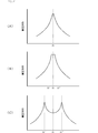
- FIGS. 7A, 7B, and 7C are schematic diagrams illustrating resonance characteristics due to multiple resonance.
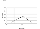
- FIG. FIG. 10 is a diagram showing the relationship between the coupling coefficient k and the voltage gain between the power feeding loop conductor Lt and the power receiving loop conductor Lr.
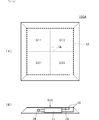
- FIG. 11A is a plan view of the power supply apparatus 102A according to the second embodiment, and FIG.
- FIG. 11B is a schematic front view showing the internal structure of the power supply apparatus 102A.
- FIG. 12 is a schematic perspective view of a wireless power transmission system 302 according to the second embodiment.
- FIG. 13 is a plan view of a power supply apparatus 102B according to the second embodiment.
- FIG. 14 is a schematic perspective view of a wireless power transmission system 303 according to the third embodiment.
- FIG. 15 is a schematic perspective view of a wireless power transmission system 304 according to the fourth embodiment.
- FIG. 1 is a schematic perspective view of a wireless power transmission system 301 according to the first embodiment.
- FIG. 2 is a schematic front view of the wireless power transmission system 301.
- the wireless power transmission system 301 includes one power supply apparatus 101 and a plurality of power receiving apparatuses 201A, 201B, and 201C.
- the power supply apparatus 101 is a game board such as a shogi board, and the power receiving apparatuses 201A, 201B, and 201C are apparatuses such as a shogi piece.
- the power feeding apparatus 101 has a first resonance circuit and an inverter circuit, and the power receiving apparatuses 201A, 201B, and 201C each have a second resonance circuit, a rectifying / smoothing circuit, and a load, as will be described later.
- the load is, for example, an LED, an IC, a motor, or the like.
- a predetermined DC power supply voltage is input to the power supply apparatus 101 by the AC adapter 13.
- the power supply apparatus 101 includes a power supply loop conductor Lt.
- the power receiving devices 201A, 201B, and 201C include a power receiving loop conductor Lr that is coupled to the power feeding loop conductor Lt mainly through a magnetic field, and a second capacitor Cr that is connected in parallel to the power receiving loop conductor Lr. A second resonance circuit is provided.
- the power supply apparatus 101 includes a power supply surface S10 that faces the opening surface of the power supply loop conductor Lt.
- the plurality of power receiving apparatuses 201A, 201B, and 201C include a power receiving surface S20 that is placed on the power feeding surface S10 with the opening surface of the power receiving loop-shaped conductor Lr facing each other.
- the power receiving apparatuses 201 ⁇ / b> A, 201 ⁇ / b> B, and 201 ⁇ / b> C are placed such that their power receiving surfaces S ⁇ b> 20 are in contact with the power feeding surface S ⁇ b> 10 of the power feeding apparatus 101.
- the power feeding apparatus 101 wirelessly transmits power to the power receiving apparatus 201A.
- the distance between the opening surface of the power receiving loop conductor Lr of the power receiving device 201A and the power receiving surface S20 is da, and the distance between the opening surface of the power receiving loop conductor Lr of the power receiving device 201B and the power receiving surface S20 is db.
- the distance between the opening surface of the power receiving loop conductor Lr of the power receiving device 201C and the power receiving surface S20 is dc.
- the distance between the power receiving loop conductor Lr and the power feeding loop conductor Lt is a distance corresponding to the weight of the load of the power receiving apparatus, and power suitable for the load is supplied to each load.
- the power receiving device 201 ⁇ / b> C is a first type power receiving device with a relatively light load that uses an LED as a load.
- the power receiving apparatus 201A is a second type power receiving apparatus that uses a motor as a load and is heavier than the load of the power receiving apparatus 201C.
- the power receiving device 201B is a device having an IC as a load, which is lighter than the power receiving device 201A and heavier than the power receiving device 201C.
- FIG. 3 is a circuit diagram of the wireless power transmission system 301. Since the electric circuits of the plurality of power receiving apparatuses 201A, 201B, and 201C are similarly represented, the power receiving apparatus represents one representative power receiving apparatus 201 here.
- the power supply apparatus 101 includes a first resonance circuit 10 including a power supply loop conductor Lt having inductance and a first capacitor Ct connected in series to the power supply loop conductor Lt.
- a first resonance circuit 10 including a power supply loop conductor Lt having inductance and a first capacitor Ct connected in series to the power supply loop conductor Lt.
- an inverter circuit 11 that converts the DC input voltage Vi into an AC voltage and applies the AC voltage to the first resonance circuit 10 is provided.
- Inverter circuit 11 includes switching elements Q1 and Q2, a capacitor C11, a diode D1, and a drive circuit 12.
- the drive circuit 12 alternately turns on / off the switching elements Q1 and Q2 at a predetermined operating frequency (for example, 6.78 MHz).
- the resonant frequency of the first resonant circuit 10 is this operating frequency or a frequency in the vicinity thereof.
- the power receiving apparatus 201 includes an inductance, a power receiving loop conductor Lr coupled to the power feeding loop conductor Lt mainly through a magnetic field, and a second capacitor Cr connected in parallel to the power receiving loop conductor Lr.
- a second resonance circuit 20 is provided.
- a rectifying / smoothing circuit 21 that converts an AC voltage generated in the second resonance circuit 20 into a DC voltage, and a load Ro that is driven by the DC output voltage converted by the rectifying / smoothing circuit 21 are provided.
- the rectifying / smoothing circuit 21 includes a rectifying circuit 22 using a diode bridge circuit, smoothing capacitors C21 and C22, and a voltage regulator circuit 23.
- the second resonance circuit 20 resonates in parallel at the above operating frequency or a frequency in the vicinity thereof.
- the resonant voltage of the second resonant circuit 20 is full-wave rectified by the rectifier circuit 22, smoothed and stabilized by the smoothing capacitors C21 and C22, and the voltage regulator circuit 23, and supplies a predetermined constant voltage to the load Ro.
- FIG. 4 is a circuit diagram of another wireless power transmission system 301V of the present embodiment.
- the diode D1 in the power receiving apparatus 201 constitutes a rectifier circuit.
- the rectifier circuit 22 shown in FIG. 3 is a full-wave rectifier circuit, whereas the diode D1 shown in FIG. 4 is a half-wave rectifier circuit.
- Other configurations are the same as those of the wireless power transmission system 301 shown in FIG.
- FIG. 5 is a diagram for explaining how the frequency characteristic of the voltage gain, which is the ratio of the DC output voltage Vo to the DC input voltage Vi, of the wireless power transmission system 301 changes depending on the difference in the equivalent resistance value of the load. It is a simplified circuit diagram.
- FIG. 6 is an equivalent circuit diagram thereof.
- the transmission AC voltage generation circuit ALT corresponds to the inverter circuit 11. 5 and 6, the rectifying / smoothing circuit 21 of the power receiving apparatus 201 and the load Ro are represented by a single load Ro.
- the power feeding loop conductor Lt and the power receiving loop conductor Lr are magnetically coupled.
- a first resonance circuit is configured by the first capacitor Ct and the inductor ⁇ (Lt ⁇ Lm) + Lm ⁇ .
- a second resonance circuit is configured by the second capacitor Cr and the inductor ⁇ (Lr ⁇ Lm) + Lm ⁇ .
- FIGS. 7A, 7B, and 7C are schematic diagrams showing the resonance characteristics due to the double resonance.
- the horizontal axis represents frequency
- the vertical axis represents voltage gain, which is the ratio of DC output voltage to DC input voltage.
- FIG. 7A shows a case where the mutual inductance Lm is ⁇ 0, which is unimodal.
- FIG. 7C shows characteristics when the mutual inductance Lm is large, and is bimodal.
- FIG. 7B shows characteristics when the mutual inductance Lm is medium, and is almost unimodal.
- the voltage gain that is the ratio of the DC output voltage to the DC input voltage becomes bimodal, and when the equivalent resistance value of the load is small, Alternatively, when the coupling coefficient (coupling degree) k is small, the frequency characteristic of the voltage gain is unimodal.
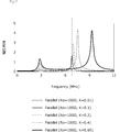
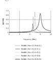
- FIG. 8 and 9 are diagrams showing frequency characteristics of voltage gain when the coupling coefficient k between the power feeding loop conductor Lt and the power receiving loop conductor Lr is changed.
- the operating frequency is 6.78 MHz
- FIG. 10 is a diagram showing the relationship between the coupling coefficient k and the voltage gain between the power feeding loop conductor Lt and the power receiving loop conductor Lr.
- the coupling coefficient k is less than the above threshold value 0.1, the coupling coefficient and the voltage gain are positively correlated.
- the distance between the power receiving loop conductor Lr and the power feeding loop conductor Lt is determined so that a coupling coefficient corresponding to the received power of the power receiving apparatus is obtained. The distance depends on the weight of the load.
- the distance between the power receiving loop conductor Lr and the power feeding loop conductor Lt shown in FIGS. 1 and 2 is a distance corresponding to the load of the power receiving apparatus.
- the load Ro of the power receiving apparatus 201A is a heavy load with a small equivalent resistance value. That is, the power receiving apparatus 201A is a second type power receiving apparatus. Therefore, the coupling coefficient k is increased by reducing the distance da between the opening surface of the power receiving loop conductor Lr of the power receiving device 201A and the power receiving surface S20. This increases the voltage gain. When the voltage gain increases, the DC output voltage Vo increases, and the power (received power) supplied to the load Ro increases.
- the load Ro of the power receiving apparatus 201C has a large equivalent resistance value and a light load. That is, the power receiving device 201C is a first type power receiving device. Therefore, the coupling coefficient k is reduced by increasing the distance dc between the opening surface of the power receiving loop conductor Lr of the power receiving device 201C and the power receiving surface S20. This reduces the voltage gain. If the voltage gain decreases, the DC output voltage Vo decreases, and the power (received power) supplied to the load Ro decreases.
- the load Ro of the power receiving apparatus 201B has a medium equivalent resistance value. Therefore, the interval db between the opening surface of the power receiving loop conductor Lr of the power receiving device 201B and the power receiving surface S20 is made smaller than the interval dc between the opening surface of the power receiving loop conductor Lr of the power receiving device 201C and the power receiving surface S20.
- the coupling coefficient k is made moderate by setting it larger than the distance da between the opening surface of the power receiving loop conductor Lr of the power receiving device 201A and the power receiving surface S20. As a result, the voltage gain is medium and the received power is medium.
- the frequency characteristics are close to unimodal, it is easy to set the received power and the received voltage gain.
- the change in frequency characteristics becomes larger than when a single power receiving device is used, and thus the setting of the power receiving voltage gain is complicated.
- Second Embodiment a wireless power transmission system in which the configuration of the power feeding apparatus is different from that in the first embodiment will be described.
- FIG. 11A is a plan view of a power feeding apparatus 102A according to the second embodiment
- FIG. 11B is a schematic front view showing an internal structure of the power feeding apparatus 102A.
- the power feeding surface S10 of the power feeding apparatus 102A is divided into four regions G11, G12, G21, and G22 on which the power receiving apparatus is placed by a dividing line GL.
- the power feeding apparatus 102 ⁇ / b> A includes a power feeding loop conductor Lt, a first capacitor Ct, an inverter circuit 11, and a DC input terminal 14.
- FIG. 12 is a schematic perspective view of the wireless power transmission system 302 according to the second embodiment.
- the power receiving apparatuses 202A, 202B, and 202C are placed in any of the four regions of the power feeding surface S10 of the power feeding apparatus 102A.
- the configurations of the power receiving apparatuses 202A, 202B, and 202C are the same as those of the power receiving apparatuses 201A, 201B, and 201C shown in the first embodiment.
- the configuration of the power supply apparatus 102A is the same as that of the power supply apparatus 101 shown in the first embodiment.
- FIG. 13 is a plan view of a power supply apparatus 102B according to the second embodiment.
- the power feeding surface of the power feeding device 102B is divided into nine regions G11, G12, G13, G21, G22, G23, G31, G32, and G33 on which the power receiving device is placed by a dividing line GL.
- the configuration of the power supply apparatus 102B is the same as that of the power supply apparatus 101 shown in the first embodiment.
- the present embodiment it is possible to predict which position in the opening surface of the power feeding loop conductor is opposed to the power receiving loop conductor, and it is easy to set the received power and the received voltage gain.
- FIG. 14 is a schematic perspective view of a wireless power transmission system 303 according to the third embodiment.
- the power receiving devices 203 ⁇ / b> A, 203 ⁇ / b> B, and 203 ⁇ / b> C are placed in any of the four regions of the power feeding surface S ⁇ b> 10 of the power feeding device 103.
- the configuration of the power supply apparatus 103 is the same as that of the power supply apparatus 102A shown in the second embodiment.
- the received power of the power receiving apparatuses 203A, 203B, and 203C is represented by Wa, Wb, and Wc
- Wa> Wb> Wc the power receiving device 203C is a first type power receiving device
- the power receiving device 203A is a second type power receiving device.
- the area of the opening surface of the power receiving loop conductor Lr of the power receiving devices 203A, 203B, and 203C is different.
- the opening areas of the power receiving loop conductor Lr of the power receiving devices 203A, 203B, and 203C are represented by Sa, Sb, and Sc
- Sa> Sb> Sc there is a relationship of Sa> Sb> Sc.
- the height from the power receiving surface S20 of the power receiving apparatus to the power receiving loop conductor Lr is also different.
- the heights from the power receiving surface S20 of the power receiving devices 203A, 203B, and 203C to the power receiving loop conductor Lr are represented by da, db, and dc, there is a relationship of da ⁇ db ⁇ dc.
- the coupling coefficient can be easily lowered by designing the power receiving loop conductor Lr so that the area of the power receiving loop conductor Lr becomes smaller as the load becomes lighter. This structure can be applied even when the height of the power receiving device is limited.
- FIG. 15 is a schematic perspective view of a wireless power transmission system 304 according to the fourth embodiment.
- the power receiving devices 204A, 204B, and 204C are placed in any one of the four regions of the power feeding surface S10 of the power feeding device 104.
- the configuration of the power supply apparatus 104 is the same as that of the power supply apparatus 102A shown in the second embodiment.
- the power receiving device 204C is a first type power receiving device
- the power receiving device 204A is a second type power receiving device.
- the number of turns of the power receiving loop conductor Lr of the power receiving devices 204A, 204B, and 204C varies depending on the difference in the received power.
- the number of turns of the power receiving loop conductor Lr of the power receiving devices 204A, 204B, and 204C is represented by na, nb, and nc, there is a relationship of na> nb> nc.
- the coupling coefficient can be easily increased by designing the power receiving loop conductor Lr so that the number of turns increases as the load increases. This structure can be applied even when the bottom area of the power receiving device is limited.
- ALT AC transmission voltage generation circuit
- C11 capacitors C21, C22: smoothing capacitor
- Ct first capacitor Cr
- second capacitor D1 diodes G11, G12, G13, G21, G22, G23, G31, G32, G33 ... region GL ... Separator Lm ... Mutual inductance Lr ... Power receiving loop conductor Lt ... Power feeding loop conductors Q1, Q2 ... Switching element Ro ... Load S10 ... Power feeding surface S20 ... Power receiving surface 10 ... First resonance circuit 11 ... Inverter circuit 12 ... Drive circuit 13 ... AC adapter 14 ... DC input terminal 20 ... second resonance circuit 21 ... rectifier smoothing circuit 22 ... rectifier circuit 23 ...
Landscapes
- Engineering & Computer Science (AREA)
- Computer Networks & Wireless Communication (AREA)
- Power Engineering (AREA)
- Charge And Discharge Circuits For Batteries Or The Like (AREA)
Abstract
給電装置(101)は、給電用ループ状導体(Lt)と第1キャパシタとを含む第1共振回路と、直流入力電圧を交流電圧に変換して前記第1共振回路に印加するインバータ回路と、を有する。受電装置(201A,201B,201C)は、給電用ループ状導体(Lt)と結合する受電用ループ状導体(Lr)と、受電用ループ状導体(Lr)に並列接続された第2キャパシタ(Cr)とを含む第2共振回路と、第2共振回路に生じる交流電圧を直流電圧に変換する整流平滑回路と、整流平滑回路によって変換された直流出力電圧によって駆動される負荷と、をそれぞれ有する。受電装置(201A,201B,201C)の、受電用ループ状導体(Lr)の開口面と受電面との間隔は負荷の軽重に応じて異なる。
Description
本発明は、給電装置から受電装置へワイヤレスで電力を伝送するワイヤレス電力伝送システムに関する。
近年、ワイヤレス給電の実用化を目指して、システム全体の電力損失を低減する研究開発が活発化している。特に、送電共振機構と受電共振機構によって電磁界共鳴フィールドを形成し、電磁界共鳴結合によりワイヤレス給電を行うシステムでは、高周波磁界を共振器に与える方式とは異なり、電力給電の過程をシンプルにして電力損失を低減できる(特許文献1参照)。
また、1台の送電装置から複数の受電装置へワイヤレスで同時に給電するように構成されたワイヤレス給電システムが特許文献2に示されている。
1台の送電装置から、複数の受電装置へワイヤレスで給電する際に、受電装置の負荷の大きさ(軽重)がそれぞれ異なる場合、特許文献2に示されるシステムでは、相互通信を事前に行って、各受電装置に対して共振回路の共振周波数をチューニングし、各受電装置が最適な電力を受電できるようにする。
ところが、各受電装置が送電装置との通信によって、各受電装置内の共振回路の共振周波数を定める方法では、送電装置への載置状態に応じて最適な共振周波数となるように可変インダクタや可変キャパシタを用いてチューニングする必要があるため、システムが複雑になり、高コスト化する。
また、1つの給電装置から、負荷の軽重が異なる複数の受電装置に電力伝送する際、負荷装置ごとに負荷の軽重が異なることに起因して、狙った周波数帯(ワイヤレス電力伝送においては、一般的に6.78MHz)での受電電圧が変化してしまい、その結果、所望の電圧(電力)を受電側に供給できない場合がある。もし、所望の電圧(電力)とするために、電圧変換装置や、ダミー抵抗等により、過剰電力を消費する回路を設けると、受電装置が大型化してしまい、小型化の妨げとなってしまう。
本発明の目的は、ワイヤレス電力伝送効率を高く維持しつつ、1つの給電装置から複数の受電装置へワイヤレスで電力を伝送する場合に、より簡易かつ小型化可能な構造で、各受電装置の負荷に適した電力を供給できるようにしたワイヤレス電力伝送システムを提供することにある。
(1)本発明のワイヤレス電力伝送システムは、
インダクタンスを有する給電用ループ状導体と、前記給電用ループ状導体に接続された第1キャパシタとを含む第1共振回路と、
直流入力電圧を交流電圧に変換して前記第1共振回路に印加するインバータ回路と、
を有する給電装置と、
インダクタンスを有し、前記給電用ループ状導体と結合する受電用ループ状導体と、前記受電用ループ状導体に並列接続された第2キャパシタとを含む第2共振回路と、
前記第2共振回路に生じる交流電圧を直流電圧に変換する整流平滑回路と、前記整流平滑回路によって変換された直流出力電圧によって駆動される負荷と、
をそれぞれ有する複数の受電装置と、
で構成されるワイヤレス電力伝送システムであって、
前記給電装置は、前記給電用ループ状導体の開口面が対向する給電面を備え、
前記複数の受電装置は、前記受電用ループ状導体の開口面が対向し、前記給電面に載置される受電面を備え、
前記複数の受電装置は、前記負荷が相対的に軽負荷である第1種受電装置と、前記負荷が前記第1種受電装置の前記負荷よりも相対的に重負荷である第2種受電装置と、を含み、
前記第1種受電装置の前記受電用ループ状導体の開口面と前記受電面との間隔をd1、前記第2種受電装置の前記受電用ループ状導体の開口面と前記受電面との間隔をd2でそれぞれ表すと、d1>d2の関係であることを特徴とする。
インダクタンスを有する給電用ループ状導体と、前記給電用ループ状導体に接続された第1キャパシタとを含む第1共振回路と、
直流入力電圧を交流電圧に変換して前記第1共振回路に印加するインバータ回路と、
を有する給電装置と、
インダクタンスを有し、前記給電用ループ状導体と結合する受電用ループ状導体と、前記受電用ループ状導体に並列接続された第2キャパシタとを含む第2共振回路と、
前記第2共振回路に生じる交流電圧を直流電圧に変換する整流平滑回路と、前記整流平滑回路によって変換された直流出力電圧によって駆動される負荷と、
をそれぞれ有する複数の受電装置と、
で構成されるワイヤレス電力伝送システムであって、
前記給電装置は、前記給電用ループ状導体の開口面が対向する給電面を備え、
前記複数の受電装置は、前記受電用ループ状導体の開口面が対向し、前記給電面に載置される受電面を備え、
前記複数の受電装置は、前記負荷が相対的に軽負荷である第1種受電装置と、前記負荷が前記第1種受電装置の前記負荷よりも相対的に重負荷である第2種受電装置と、を含み、
前記第1種受電装置の前記受電用ループ状導体の開口面と前記受電面との間隔をd1、前記第2種受電装置の前記受電用ループ状導体の開口面と前記受電面との間隔をd2でそれぞれ表すと、d1>d2の関係であることを特徴とする。
上記構成により、受電用ループ状導体と給電用ループ状導体との距離が、受電装置の負荷の軽重に応じた距離となって、各負荷に適した電力が供給される。
(2)上記(1)において、前記給電面は前記受電装置が載置される領域ごとに区分されていることが好ましい。これにより、給電用ループ状導体の開口面内のどの位置に受電用ループ状導体が対向するかを予測でき、受電電力や受電電圧利得の設定がしやすくなる。
(3)上記(1)または(2)において、前記第1種受電装置の前記受電用ループ状導体の開口面の面積をS1、前記第2種受電装置の前記受電用ループ状導体の開口面の面積をS2でそれぞれ表すと、S1<S2の関係にあることが好ましい。このことにより、高さ方向に制限がある場合でも、受電用ループ状導体の面積を軽負荷になるほど小さくなるように設計することで結合係数を容易に下げることができる。
(4)上記(1)から(3)のいずれかにおいて、前記第1種受電装置の前記受電用ループ状導体のターン数をn1、前記第2種受電装置の前記受電用ループ状導体のターン数をn2でそれぞれ表すと、n1<n2の関係にあることが好ましい。このことにより、受電装置の受電面の面積に制限がある場合でも、受電用ループ状導体のターン数を、軽負荷になるほど少なくすることで、結合係数を容易に下げることができる。
本発明によれば、負荷の軽重の異なる複数種の受電装置が存在する場合でも、各受電装置の負荷に対して適した電力が供給される。
以降、図を参照して幾つかの具体的な例を挙げて、本発明を実施するための複数の形態を示す。各図中には同一箇所に同一符号を付している。要点の説明または理解の容易性を考慮して、便宜上実施形態を分けて示すが、異なる実施形態で示した構成の部分的な置換または組み合わせが可能である。第2の実施形態以降では第1の実施形態と共通の事柄についての記述を省略し、異なる点についてのみ説明する。特に、同様の構成による同様の作用効果については実施形態毎には逐次言及しない。
《第1の実施形態》
図1は第1の実施形態に係るワイヤレス電力伝送システム301の概略斜視図である。図2はワイヤレス電力伝送システム301の概略正面図である。このワイヤレス電力伝送システム301は、一つの給電装置101と複数の受電装置201A,201B,201Cを備える。給電装置101は例えば将棋盤のようなゲームボードであり、受電装置201A,201B,201C等は例えば将棋のコマのような装置である。
図1は第1の実施形態に係るワイヤレス電力伝送システム301の概略斜視図である。図2はワイヤレス電力伝送システム301の概略正面図である。このワイヤレス電力伝送システム301は、一つの給電装置101と複数の受電装置201A,201B,201Cを備える。給電装置101は例えば将棋盤のようなゲームボードであり、受電装置201A,201B,201C等は例えば将棋のコマのような装置である。
給電装置101は、後に示すとおり、第1共振回路とインバータ回路を有し、受電装置201A,201B,201Cは、第2共振回路、整流平滑回路および負荷をそれぞれ有する。負荷は例えばLED、IC、モータ等である。
給電装置101にはACアダプタ13によって、所定のDC電源電圧が入力される。給電装置101は給電用ループ状導体Ltを備える。受電装置201A,201B,201Cは、給電用ループ状導体Ltと主に磁界を介して結合する受電用ループ状導体Lrと、受電用ループ状導体Lrに並列接続された第2キャパシタCrとを含む第2共振回路を備える。
給電装置101は、給電用ループ状導体Ltの開口面が対向する給電面S10を備える。複数の受電装置201A,201B,201Cは、受電用ループ状導体Lrの開口面が対向し、給電面S10に載置される受電面S20を備える。
受電装置201A,201B,201Cは、それらの受電面S20が給電装置101の給電面S10に接するように載置される。例えば、受電装置201Aが給電装置101に載置されると、給電装置101は受電装置201Aへワイヤレス電力伝送する。
受電装置201Aの受電用ループ状導体Lrの開口面と受電面S20との間隔はdaであり、受電装置201Bの受電用ループ状導体Lrの開口面と受電面S20との間隔はdbであり、受電装置201Cの受電用ループ状導体Lrの開口面と受電面S20との間隔はdcである。後に説明するように、受電用ループ状導体Lrと給電用ループ状導体Ltとの距離が、受電装置の負荷の軽重に応じた距離となっていて、各負荷にはそれに適した電力が供給される。受電装置201Cは、LEDを負荷とする、相対的に軽負荷の第1種受電装置である。受電装置201Aはモータを負荷とする、受電装置201Cの負荷より重負荷の第2種受電装置である。受電装置201BはICを負荷とする装置であり、受電装置201Aよりも軽負荷であり、受電装置201Cよりも重負荷である。
図3はワイヤレス電力伝送システム301の回路図である。複数の受電装置201A,201B,201Cの電気回路は同様に表されるので、受電装置については、ここでは代表する一つの受電装置201を表している。
給電装置101は、インダクタンスを有する給電用ループ状導体Ltと、給電用ループ状導体Ltに直列接続された第1キャパシタCtとを含む第1共振回路10を備える。また、直流入力電圧Viを交流電圧に変換して第1共振回路10に印加するインバータ回路11を備える。インバータ回路11は、スイッチング素子Q1,Q2、キャパシタC11、ダイオードD1および駆動回路12を含む。駆動回路12は、スイッチング素子Q1,Q2を所定の動作周波数(例えば6.78MHz)で交互にオン/オフ駆動する。第1共振回路10の共振周波数はこの動作周波数またはその近傍の周波数である。
受電装置201は、インダクタンスを有し、給電用ループ状導体Ltと主に磁界を介して結合する受電用ループ状導体Lrと、受電用ループ状導体Lrに並列接続された第2キャパシタCrとを含む第2共振回路20を備える。また、第2共振回路20に生じる交流電圧を直流電圧に変換する整流平滑回路21と、整流平滑回路21によって変換された直流出力電圧によって駆動される負荷Roとを備える。整流平滑回路21はダイオードブリッジ回路による整流回路22、平滑キャパシタC21,C22、および電圧レギュレータ回路23を含む。
第2共振回路20は上記動作周波数またはその近傍の周波数で並列共振する。第2共振回路20の共振電圧は整流回路22で全波整流され、平滑キャパシタC21,C22、および電圧レギュレータ回路23で平滑および安定化され、負荷Roへ所定の一定電圧を供給する。
図4は、本実施形態の別のワイヤレス電力伝送システム301Vの回路図である。この例では、受電装置201内のダイオードD1は整流回路を構成する。図3に示した整流回路22は全波整流回路であるのに対し、図4に示すダイオードD1は半波整流回路である。その他の構成は図3に示したワイヤレス電力伝送システム301と同じである。
図5は、ワイヤレス電力伝送システム301の、直流入力電圧Viに対する直流出力電圧Voの比である電圧利得の周波数特性が、負荷の等価抵抗値の違いによってどのように変化するかを説明するための簡略回路図である。また、図6はその等価回路図である。
図5、図6において、送電交流電圧発生回路ALTはインバータ回路11に相当する。また、図5、図6においては、受電装置201の整流平滑回路21と負荷Roとを一つの負荷Roで表している。給電用ループ状導体Ltと受電用ループ状導体Lrは磁界結合する。
図6において、送電交流電圧発生回路ALTのインピーダンスが無視できる程度に小さいものとすると、第1キャパシタCtおよびインダクタ{(Lt-Lm)+Lm}による第1の共振回路が構成される。また、負荷の等価抵抗値が小さいと、第2キャパシタCrおよびインダクタ{(Lr-Lm)+Lm}による第2の共振回路が構成される。
このように、二つの共振回路が存在し、相互インダクタンスLmを介して結合するので、複合共振回路が構成され、偶モードと奇モードの共振モードが生じる。
ここで、給電用ループ状導体Ltのインダクタンスと受電用ループ状導体LrのインダクタンスをいずれもLで表し、第1キャパシタCt、第2キャパシタCrのキャパシタンスをいずれもCで表すと、次の2つの共振周波数f1',f1"が生じる。
f1'=1/(2π√(L+Lm)C)
f1"=1/(2π√(L-Lm)C)
給電用ループ状導体Ltの自己インダクタンスをLt、受電用ループ状導体Lrの自己インダクタンスをLr、結合係数をkで表すと、給電用ループ状導体Ltと受電用ループ状導体Lrとの結合による相互インダクタンスLmは、
Lm=k√(Lt・Lr) の関係にある。
f1"=1/(2π√(L-Lm)C)
給電用ループ状導体Ltの自己インダクタンスをLt、受電用ループ状導体Lrの自己インダクタンスをLr、結合係数をkで表すと、給電用ループ状導体Ltと受電用ループ状導体Lrとの結合による相互インダクタンスLmは、
Lm=k√(Lt・Lr) の関係にある。
図7(A)(B)(C)は、上記複共振による共振特性を示す概略図である。いずれも横軸は周波数、縦軸は直流入力電圧に対する直流出力電圧の比である電圧利得である。図7(A)は相互インダクタンスLmが≒0のときであり、単峰性となる。図7(C)は相互インダクタンスLmが大きいときの特性であり、双峰性となる。図7(B)は相互インダクタンスLmが中程度であるときの特性であり、ほぼ単峰性である。
図6に示した負荷Roの等価抵抗値が大きいとき、すなわち軽負荷であるときは、複共振が生じるので、電圧利得の周波数特性は図7(C)に示すような双峰性となる。負荷Roの等価抵抗値が小さいとき、すなわち重負荷であるときは、複共振は生じないので、電圧利得の周波数特性は、上記第1共振回路の共振周波数で電圧利得がピークになる単峰性となる。
したがって、負荷の等価抵抗値が大きく、且つ結合係数(結合度)kが大きいとき、直流入力電圧に対する直流出力電圧の比である電圧利得は双峰性となり、負荷の等価抵抗値が小さいとき、または、結合係数(結合度)kが小さいとき、電圧利得の周波数特性は単峰性となる。
図8、図9は、給電用ループ状導体Ltと受電用ループ状導体Lrとの結合係数kを変化させたときの電圧利得の周波数特性を示す図である。図8は、負荷Roの等価抵抗値=100Ω(大きい値)のときの特性、図9は、負荷Roの等価抵抗値=1Ω(小さい値)のときの特性である。いずれも、結合係数kを0.01から0.65まで5段階に変化させている。
負荷の等価抵抗値が大きいとき、図8に表れているように、上述の複合共振が生じて、電圧利得の周波数特性は双峰性となる。
図8、図9に示す例で、動作周波数が6.78MHzであれば、負荷の等価抵抗値が小さい受電装置、負荷の等価抵抗値が大きい受電装置のいずれについても、結合係数kが或るしきい値より小さいと(図8、図9に示した例ではk<0.1)、結合係数kが小さい程、電圧利得は小さくなる。そして、結合係数kが上記しきい値より大きくなる程、電圧利得のピーク周波数は高域へシフトするので、電圧利得は再び小さくなる。
図10は、給電用ループ状導体Ltと受電用ループ状導体Lrとの結合係数kと電圧利得との関係を示す図である。結合係数kが上記しきい値0.1未満では、結合係数と電圧利得は正の相関関係にある。本実施形態では、この部分の特性を利用して、受電装置の受電電力に応じた結合係数が得られるように、受電用ループ状導体Lrと給電用ループ状導体Ltとの距離を、受電装置の負荷の軽重に応じた距離としている。
図1、図2に示した、受電用ループ状導体Lrと給電用ループ状導体Ltとの距離は、受電装置の負荷の軽重に応じた距離となっている。
受電装置201Aの負荷Roは等価抵抗値が小さく重負荷である。すなわち、受電装置201Aは第2種受電装置である。そのため、受電装置201Aの受電用ループ状導体Lrの開口面と受電面S20との間隔daを小さくすることにより、結合係数kを大きくする。このことにより、電圧利得が大きくなる。電圧利得が大きくなれば、直流出力電圧Voが高くなり、負荷Roに供給される電力(受電電力)は大きくなる。
受電装置201Cの負荷Roは等価抵抗値が大きく軽負荷である。すなわち、受電装置201Cは第1種受電装置である。そのため、受電装置201Cの受電用ループ状導体Lrの開口面と受電面S20との間隔dcを大きくすることにより、結合係数kを小さくする。このことにより、電圧利得が小さくなる。電圧利得が小さくなれば、直流出力電圧Voが低くなり、負荷Roに供給される電力(受電電力)は小さくなる。
受電装置201Bの負荷Roは等価抵抗値が中程度である。そのため、受電装置201Bの受電用ループ状導体Lrの開口面と受電面S20との間隔dbを、受電装置201Cの受電用ループ状導体Lrの開口面と受電面S20との間隔dcよりも小さくし、受電装置201Aの受電用ループ状導体Lrの開口面と受電面S20との間隔daよりも大きくすることにより、結合係数kを中程度にする。このことにより、電圧利得は中程度となり、受電電力は中程度となる。
したがって、上記3つの間隔は、da<db<dcの関係である。このことで、受電装置201A,201B,201Cの各負荷Roに適した(必要な)電力が供給される。
また、周波数特性が単峰性に近づくため、受電電力や受電電圧利得の設定がしやすくなる。特に、複数の受電装置を送電装置に配置する場合、受電装置が単数である場合に比べ周波数特性の変化が大きくなるため、受電電圧利得の設定が複雑になる。受電装置の共振周波数を動作周波数に設定し、周波数特性が単峰性となる範囲で上記間隔を調整することで受電電圧利得の設定の難易度を低減できる。
《第2の実施形態》
第2の実施形態では、給電装置の構成が第1の実施形態とは異なるワイヤレス電力伝送システムについて示す。
第2の実施形態では、給電装置の構成が第1の実施形態とは異なるワイヤレス電力伝送システムについて示す。
図11(A)は第2の実施形態に係る給電装置102Aの平面図、図11(B)は給電装置102Aの内部構造を示す概略正面図である。給電装置102Aの給電面S10は、区切線GLによって、受電装置が載置される4つの領域G11,G12,G21,G22に区分されている。給電装置102Aには、給電用ループ状導体Lt、第1キャパシタCt、インバータ回路11、およびDC入力端子14を備える。
図12は第2の実施形態に係るワイヤレス電力伝送システム302の概略斜視図である。受電装置202A,202B,202Cは、給電装置102Aの給電面S10の4つの領域のいずれかに載置される。受電装置202A,202B,202Cの構成は第1の実施形態で示した受電装置201A,201B,201Cと同じである。給電装置102Aの構成は第1の実施形態で示した給電装置101と同じである。
図13は第2の実施形態に係る給電装置102Bの平面図である。給電装置102Bの給電面は、区切線GLによって、受電装置が載置される9つの領域G11,G12,G13,G21,G22,G23,G31,G32,G33に区分されている。給電装置102Bの構成は第1の実施形態で示した給電装置101と同じである。
本実施形態によれば、給電用ループ状導体の開口面内のどの位置に受電用ループ状導体が対向するかを予測でき、受電電力や受電電圧利得の設定がしやすくなる。
《第3の実施形態》
第3の実施形態では、受電装置の構成が第1の実施形態とは異なるワイヤレス電力伝送システムについて示す。
第3の実施形態では、受電装置の構成が第1の実施形態とは異なるワイヤレス電力伝送システムについて示す。
図14は第3の実施形態に係るワイヤレス電力伝送システム303の概略斜視図である。受電装置203A,203B,203Cは、給電装置103の給電面S10の4つの領域のいずれかに載置される。給電装置103の構成は第2の実施形態で示した給電装置102Aと同じである。
受電装置203A,203B,203Cの受電電力をWa,Wb,Wcで表すと、Wa>Wb>Wcの関係にある。すなわち、受電装置203Cは第1種受電装置であり、受電装置203Aは第2種受電装置である。このような受電電力の違いに応じて、受電装置203A,203B,203Cの受電用ループ状導体Lrの開口面の面積はそれぞれ異なる。受電装置203A,203B,203Cの受電用ループ状導体Lrの開口面積をSa,Sb,Scで表すと、Sa>Sb>Scの関係にある。また、本実施形態では、受電装置の受電面S20から受電用ループ状導体Lrまでの高さも異なる。受電装置203A,203B,203Cの受電面S20から受電用ループ状導体Lrまでの高さをda,db,dcで表すと、da<db<dcの関係にある。
このように、受電用ループ状導体Lrの面積を軽負荷になるほど小さくなるように設計することで、結合係数を容易に下げることができる。受電装置の高さ寸法に制限がある場合でも、本構造は適用できる。
《第4の実施形態》
第4の実施形態では、受電装置の構成が第1の実施形態とは異なるワイヤレス電力伝送システムについて示す。
第4の実施形態では、受電装置の構成が第1の実施形態とは異なるワイヤレス電力伝送システムについて示す。
図15は第4の実施形態に係るワイヤレス電力伝送システム304の概略斜視図である。受電装置204A,204B,204Cは、給電装置104の給電面S10の4つの領域のいずれかに載置される。給電装置104の構成は第2の実施形態で示した給電装置102Aと同じである。
受電装置204A,204B,204Cの受電電力をWa,Wb,Wcで表すと、Wa>Wb>Wcの関係にある。すなわち、受電装置204Cは第1種受電装置であり、受電装置204Aは第2種受電装置である。このような受電電力の違いに応じて、受電装置204A,204B,204Cの受電用ループ状導体Lrのターン数はそれぞれ異なる。受電装置204A,204B,204Cの受電用ループ状導体Lrのターン数をna,nb,ncで表すと、na>nb>ncの関係にある。
このように、受電用ループ状導体Lrのターン数を重負荷になるほど多くするように設計することで、結合係数を容易に上げることができる。受電装置の底面積に制限がある場合でも、本構造は適用できる。
最後に、上述の実施形態の説明は、すべての点で例示であって、制限的なものではない。当業者にとって変形および変更が適宜可能である。例えば、異なる実施形態で示した構成の部分的な置換または組み合わせが可能である。本発明の範囲は、上述の実施形態ではなく、特許請求の範囲によって示される。さらに、本発明の範囲には、特許請求の範囲と均等の意味および範囲内でのすべての変更が含まれることが意図される。
ALT…送電交流電圧発生回路
C11…キャパシタ
C21,C22…平滑キャパシタ
Ct…第1キャパシタ
Cr…第2キャパシタ
D1…ダイオード
G11,G12,G13,G21,G22,G23,G31,G32,G33…領域
GL…区切線
Lm…相互インダクタンス
Lr…受電用ループ状導体
Lt…給電用ループ状導体
Q1,Q2…スイッチング素子
Ro…負荷
S10…給電面
S20…受電面
10…第1共振回路
11…インバータ回路
12…駆動回路
13…ACアダプタ
14…DC入力端子
20…第2共振回路
21…整流平滑回路
22…整流回路
23…電圧レギュレータ回路
101,102A,102B,103,104…給電装置
201,201A,201B,201C…受電装置
202A,202B,202C…受電装置
203A,203B,203C…受電装置
204A,204B,204C…受電装置
301,301V,302,303,304…ワイヤレス電力伝送システム
C11…キャパシタ
C21,C22…平滑キャパシタ
Ct…第1キャパシタ
Cr…第2キャパシタ
D1…ダイオード
G11,G12,G13,G21,G22,G23,G31,G32,G33…領域
GL…区切線
Lm…相互インダクタンス
Lr…受電用ループ状導体
Lt…給電用ループ状導体
Q1,Q2…スイッチング素子
Ro…負荷
S10…給電面
S20…受電面
10…第1共振回路
11…インバータ回路
12…駆動回路
13…ACアダプタ
14…DC入力端子
20…第2共振回路
21…整流平滑回路
22…整流回路
23…電圧レギュレータ回路
101,102A,102B,103,104…給電装置
201,201A,201B,201C…受電装置
202A,202B,202C…受電装置
203A,203B,203C…受電装置
204A,204B,204C…受電装置
301,301V,302,303,304…ワイヤレス電力伝送システム
Claims (4)
- インダクタンスを有する給電用ループ状導体と、前記給電用ループ状導体に接続された第1キャパシタとを含む第1共振回路と、
直流入力電圧を交流電圧に変換して前記第1共振回路に印加するインバータ回路と、
を有する給電装置と、
インダクタンスを有し、前記給電用ループ状導体と結合する受電用ループ状導体と、前記受電用ループ状導体に並列接続された第2キャパシタとを含む第2共振回路と、
前記第2共振回路に生じる交流電圧を直流電圧に変換する整流平滑回路と、前記整流平滑回路によって変換された直流出力電圧によって駆動される負荷と、
をそれぞれ有する複数の受電装置と、
で構成されるワイヤレス電力伝送システムであって、
前記給電装置は、前記給電用ループ状導体の開口面が対向する給電面を備え、
前記複数の受電装置は、前記受電用ループ状導体の開口面が対向し、前記給電面に載置される受電面を備え、
前記複数の受電装置は、前記負荷が相対的に軽負荷である第1種受電装置と、前記負荷が前記第1種受電装置の前記負荷よりも相対的に重負荷である第2種受電装置と、を含み、
前記第1種受電装置の前記受電用ループ状導体の開口面と前記受電面との間隔をd1、前記第2種受電装置の前記受電用ループ状導体の開口面と前記受電面との間隔をd2でそれぞれ表すと、d1>d2の関係であることを特徴とするワイヤレス電力伝送システム。 - 前記給電面は前記受電装置が載置される領域ごとに区分されている、請求項1に記載のワイヤレス電力伝送システム。
- 前記第1種受電装置の前記受電用ループ状導体の開口面の面積をS1、前記第2種受電装置の前記受電用ループ状導体の開口面の面積をS2でそれぞれ表すと、S1<S2の関係にある、請求項1または2に記載のワイヤレス電力伝送システム。
- 前記第1種受電装置の前記受電用ループ状導体のターン数をn1、前記第2種受電装置の前記受電用ループ状導体のターン数をn2でそれぞれ表すと、n1<n2の関係にある、請求項1から3のいずれかに記載のワイヤレス電力伝送システム。
Priority Applications (1)
| Application Number | Priority Date | Filing Date | Title |
|---|---|---|---|
| JP2017520607A JPWO2016190094A1 (ja) | 2015-05-25 | 2016-05-11 | ワイヤレス電力伝送システム |
Applications Claiming Priority (2)
| Application Number | Priority Date | Filing Date | Title |
|---|---|---|---|
| JP2015105329 | 2015-05-25 | ||
| JP2015-105329 | 2015-05-25 |
Publications (1)
| Publication Number | Publication Date |
|---|---|
| WO2016190094A1 true WO2016190094A1 (ja) | 2016-12-01 |
Family
ID=57393870
Family Applications (1)
| Application Number | Title | Priority Date | Filing Date |
|---|---|---|---|
| PCT/JP2016/063947 Ceased WO2016190094A1 (ja) | 2015-05-25 | 2016-05-11 | ワイヤレス電力伝送システム |
Country Status (2)
| Country | Link |
|---|---|
| JP (1) | JPWO2016190094A1 (ja) |
| WO (1) | WO2016190094A1 (ja) |
Cited By (1)
| Publication number | Priority date | Publication date | Assignee | Title |
|---|---|---|---|---|
| CN111769657A (zh) * | 2020-07-24 | 2020-10-13 | Tcl通力电子(惠州)有限公司 | 无线充电接收电路及无线充电接收装置 |
Citations (4)
| Publication number | Priority date | Publication date | Assignee | Title |
|---|---|---|---|---|
| JP2000069685A (ja) * | 1998-08-26 | 2000-03-03 | Matsushita Electric Works Ltd | 非接触充電装置,非接触充電式電動歯ブラシ |
| JP2000184606A (ja) * | 1998-12-11 | 2000-06-30 | Sanyo Electric Co Ltd | 非接触充電器の充電電流制御方法および装置 |
| JP2014072963A (ja) * | 2012-09-28 | 2014-04-21 | Nec Saitama Ltd | 非接触充電器および非接触充電システム |
| JP2015505239A (ja) * | 2012-01-24 | 2015-02-16 | アクセス ビジネス グループ インターナショナル リミテッド ライアビリティ カンパニー | 無線電力コントロール・システム |
Family Cites Families (2)
| Publication number | Priority date | Publication date | Assignee | Title |
|---|---|---|---|---|
| JPH05234763A (ja) * | 1991-06-28 | 1993-09-10 | Matsushita Electric Works Ltd | 充電式電気機器 |
| JPH0919078A (ja) * | 1995-06-27 | 1997-01-17 | Omron Corp | 電磁誘導式充電装置、被充電電子機器及び電動歯ブラシ |
-
2016
- 2016-05-11 JP JP2017520607A patent/JPWO2016190094A1/ja active Pending
- 2016-05-11 WO PCT/JP2016/063947 patent/WO2016190094A1/ja not_active Ceased
Patent Citations (4)
| Publication number | Priority date | Publication date | Assignee | Title |
|---|---|---|---|---|
| JP2000069685A (ja) * | 1998-08-26 | 2000-03-03 | Matsushita Electric Works Ltd | 非接触充電装置,非接触充電式電動歯ブラシ |
| JP2000184606A (ja) * | 1998-12-11 | 2000-06-30 | Sanyo Electric Co Ltd | 非接触充電器の充電電流制御方法および装置 |
| JP2015505239A (ja) * | 2012-01-24 | 2015-02-16 | アクセス ビジネス グループ インターナショナル リミテッド ライアビリティ カンパニー | 無線電力コントロール・システム |
| JP2014072963A (ja) * | 2012-09-28 | 2014-04-21 | Nec Saitama Ltd | 非接触充電器および非接触充電システム |
Cited By (1)
| Publication number | Priority date | Publication date | Assignee | Title |
|---|---|---|---|---|
| CN111769657A (zh) * | 2020-07-24 | 2020-10-13 | Tcl通力电子(惠州)有限公司 | 无线充电接收电路及无线充电接收装置 |
Also Published As
| Publication number | Publication date |
|---|---|
| JPWO2016190094A1 (ja) | 2017-11-02 |
Similar Documents
| Publication | Publication Date | Title |
|---|---|---|
| CN103283120B (zh) | 用于无线功率传输的系统 | |
| JP5934935B2 (ja) | 無線電力伝送システム | |
| US8716899B2 (en) | Power receiving apparatus and wireless power transceiving system | |
| US10158254B2 (en) | Resonant coupling power transmission system, resonance type power transmission device, and resonance type power reception device | |
| JP6023785B2 (ja) | 無線電力送信の制御方法、及び無線電力送信装置 | |
| US20190140485A1 (en) | Wireless power transmission apparatus and wireless power transmission method | |
| US10529484B2 (en) | Coil device of wireless power transfer system | |
| JP5550785B2 (ja) | 非接触型の誘導電力伝送システムの回路 | |
| KR20110108596A (ko) | 전력 수신장치 및 무선전력 송수신시스템 | |
| JP2019535224A (ja) | 無線電力伝送装置、無線電力送信システム、及び無線電力送信システムを駆動する方法 | |
| WO2013080531A1 (ja) | 無線電力伝送装置 | |
| JP2019530408A (ja) | 無線電力伝送装置、無線電力送信システム、及び無線電力送信システムを駆動する方法 | |
| JP6094820B2 (ja) | 無線電力伝送装置 | |
| JP6315109B2 (ja) | 給電装置 | |
| JP2020156302A (ja) | 非接触給電装置 | |
| KR101976613B1 (ko) | 무선전력 수신장치 | |
| KR102560807B1 (ko) | 공진 모듈 및 그를 이용한 무선 전력 송신 장치 | |
| WO2016190094A1 (ja) | ワイヤレス電力伝送システム | |
| WO2020189351A1 (ja) | 非接触給電装置 | |
| US9979315B2 (en) | Rectifying circuit for high-frequency power supply | |
| CN119276021A (zh) | 一种具有全向抗位置偏移能力的水下航行器无线电能传输系统 | |
| CN110383632B (zh) | 谐振型功率发送装置及谐振型功率传输系统 | |
| KR101438888B1 (ko) | 무선전력 송신장치 및 무선전력 전송 시스템 | |
| JP2025002354A (ja) | 非接触給電装置及び受電装置 | |
| KR102428009B1 (ko) | 무선 전력 송신 장치 |
Legal Events
| Date | Code | Title | Description |
|---|---|---|---|
| 121 | Ep: the epo has been informed by wipo that ep was designated in this application |
Ref document number: 16799802 Country of ref document: EP Kind code of ref document: A1 |
|
| ENP | Entry into the national phase |
Ref document number: 2017520607 Country of ref document: JP Kind code of ref document: A |
|
| NENP | Non-entry into the national phase |
Ref country code: DE |
|
| 122 | Ep: pct application non-entry in european phase |
Ref document number: 16799802 Country of ref document: EP Kind code of ref document: A1 |