WO2016182020A1 - インバータ制御方法、インバータ装置、半導体装置 - Google Patents
インバータ制御方法、インバータ装置、半導体装置 Download PDFInfo
- Publication number
- WO2016182020A1 WO2016182020A1 PCT/JP2016/064140 JP2016064140W WO2016182020A1 WO 2016182020 A1 WO2016182020 A1 WO 2016182020A1 JP 2016064140 W JP2016064140 W JP 2016064140W WO 2016182020 A1 WO2016182020 A1 WO 2016182020A1
- Authority
- WO
- WIPO (PCT)
- Prior art keywords
- layer
- light emitting
- inverter
- output
- semiconductor switching
- Prior art date
- Legal status (The legal status is an assumption and is not a legal conclusion. Google has not performed a legal analysis and makes no representation as to the accuracy of the status listed.)
- Ceased
Links
Images


Classifications
-
- H—ELECTRICITY
- H02—GENERATION; CONVERSION OR DISTRIBUTION OF ELECTRIC POWER
- H02M—APPARATUS FOR CONVERSION BETWEEN AC AND AC, BETWEEN AC AND DC, OR BETWEEN DC AND DC, AND FOR USE WITH MAINS OR SIMILAR POWER SUPPLY SYSTEMS; CONVERSION OF DC OR AC INPUT POWER INTO SURGE OUTPUT POWER; CONTROL OR REGULATION THEREOF
- H02M7/00—Conversion of AC power input into DC power output; Conversion of DC power input into AC power output
- H02M7/42—Conversion of DC power input into AC power output without possibility of reversal
- H02M7/44—Conversion of DC power input into AC power output without possibility of reversal by static converters
- H02M7/48—Conversion of DC power input into AC power output without possibility of reversal by static converters using discharge tubes with control electrode or semiconductor devices with control electrode
-
- H—ELECTRICITY
- H10—SEMICONDUCTOR DEVICES; ELECTRIC SOLID-STATE DEVICES NOT OTHERWISE PROVIDED FOR
- H10F—INORGANIC SEMICONDUCTOR DEVICES SENSITIVE TO INFRARED RADIATION, LIGHT, ELECTROMAGNETIC RADIATION OF SHORTER WAVELENGTH OR CORPUSCULAR RADIATION
- H10F55/00—Radiation-sensitive semiconductor devices covered by groups H10F10/00, H10F19/00 or H10F30/00 being structurally associated with electric light sources and electrically or optically coupled thereto
Definitions
- the present invention relates to an inverter control method, an inverter device, and a semiconductor device.
- power devices used in the field of power conversion and control are called power devices, and include rectifier diodes, power transistors (power MOSFETs, insulated gate bipolar transistors (IGBTs)), thyristors, gate turn-off thyristors (GTOs), and the like. Generally known.
- an inverter method is generally adopted in which the input power from the power supply is converted into alternating current of a desired frequency and the frequency is controlled, but the inverter control is performed by switching an IGBT, a MOSFET, or the like.
- Mainly used are pulse width modulation (PWM) and pulse frequency modulation (PFM).
- the IGBT has a problem of switching loss caused by a transient state at turn-on or turn-off.
- PWM pulse width modulation
- PFM pulse frequency modulation
- the present invention is an example of a problem to deal with such a problem. That is, inverter control can be realized by driving at a low frequency, reducing noise and energy loss accompanying switching loss, obtaining a low-cost semiconductor device with a simple structure, and the like. Is the purpose.
- an inverter control method, an inverter device, and a semiconductor device of the present invention have the following configurations.
- An inverter control method for obtaining an output waveform by synthesizing output voltages of a plurality of semiconductor switching elements subjected to switching control, wherein the output voltage of each of the semiconductor switching elements is a pulse waveform having a constant voltage level at a constant period.
- the inverter control method is characterized in that the output voltages of all the semiconductor switching elements are controlled so as to have the same voltage level in the same cycle, different duty ratios, and coincide with the center timing of the pulse width.
- An inverter device comprising a plurality of semiconductor switching elements connected in parallel to a DC power source and a control unit for controlling the output voltages of the plurality of semiconductor switching elements, and combining the output voltages to obtain an output waveform.
- the control unit sets each output voltage to a pulse waveform having a constant voltage level in a constant cycle, and all the output waveforms have the same voltage level in the same cycle, different duty ratios, and the center timing of the pulse width is An inverter device that is controlled to match.
- a common collector electrode a collector layer that is laminated directly or via another layer on the collector electrode, a common layer that conducts electricity to the collector electrode, and a layer that is laminated on the collector layer and divided into a plurality of regions.
- a phototransistor array comprising: a base layer having a light receiving portion in each divided region; an emitter layer individually stacked on the divided base layer; and a common emitter electrode for energizing the emitter layer;
- a semiconductor device comprising: a light emitting element array in which light emitting elements that pass through the emitter electrode and enter light into the light receiving unit are arranged in each of the plurality of regions; and a control unit that individually controls the light emitting elements. .
- the present invention having such characteristics can realize inverter control by driving at a low frequency, and can reduce noise and energy loss accompanying switching loss.
- a low-cost semiconductor device can be obtained with a simple structure.
- FIG. 4 is a sectional view taken along line XX in FIG. 3. It is explanatory drawing which showed an example of the control system of the semiconductor device which concerns on embodiment of this invention.
- the inverter device 100 includes an inverter circuit 100A including a plurality of semiconductor switching elements 102 connected in parallel to the DC power source 101, and a control unit 103 that controls output voltages of the plurality of semiconductor switching elements 102.
- the inverter circuit 100A includes four semiconductor switching elements 102, but the number is not particularly limited, and an output waveform closer to a sine wave can be obtained by increasing the number.
- the semiconductor switching element 102 of the inverter circuit 100A is an IGBT in the illustrated example, and a free-wheeling diode 104 is connected in reverse parallel between its collector and emitter.
- an adjustment resistor 105 is connected in series to the output terminal (emitter terminal) of each semiconductor switching element 102, and each adjustment resistor 105 is connected in parallel to the output terminal 100B of the inverter circuit 100A.
- the semiconductor switching element 102 is not limited to the IGBT, and may be any element that can perform a switching operation, such as a power MOSFET.
- the control unit 103 controls the switching of each semiconductor switching element 102 by controlling the gate voltage of the semiconductor switching element 102.
- the output voltage of each semiconductor switching element 102 that is subjected to switching control by the control unit 103 becomes a pulse waveform (square wave) at a constant voltage level at a constant cycle, and this output voltage is synthesized to generate an output waveform of the inverter circuit 100A. Output from the output terminal 100B.
- the inverter device 100 includes a step-up transformer 110 in which resonance capacitors 111 and 112 are connected in parallel on the primary side and the secondary side, respectively, to the output terminal 100B of the inverter circuit 100A, and a single-phase output waveform. It is connected to a load (such as a motor) via a phase converter 120 that converts to a phase output waveform.
- a load such as a motor
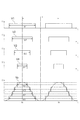
- V1, V2, V3, and V4 shown in FIG. 2 indicate output voltages of the plurality of semiconductor switches 102 controlled by the control unit 103 (the vertical axis V is voltage and the horizontal axis t is time).
- Each of the output voltages V1, V2, V3, and V4 is a pulse waveform having a constant voltage level at a constant cycle, and all the output voltages V1 to V4 are at the same voltage level and have different duty ratios ( Have different pulse widths).
- the output voltages V1 to V4 are controlled so that the center timings ts of the pulse widths W1 to W4 coincide with each other, and the output voltages V1 to V4 are between the maximum width (W1) and the minimum width (W4). Have different pulse widths in stages.
- a stepped output waveform Vo obtained by adding the levels of the output voltages V1 to V4 is obtained at the output terminal 100B of the inverter circuit 100A.
- n is one of natural numbers from 1 to N)
- the pulse width W1 of the output voltage V1 is 2W 0 ⁇ sin ⁇ 1 (1/8), and the pulse width W2 of the output voltage V2 is 2W 0 ⁇ sin ⁇ 1 (3/8),
- the pulse width W3 of the output voltage V3 is 2W 0 ⁇ sin ⁇ 1 (5/8), and the pulse width W4 of the output voltage V4 is 2W 0 ⁇ sin ⁇ 1 (7/8).
- the number N of the semiconductor switching elements 102 may be increased, and the switching frequency of the semiconductor switching elements 102 does not need to be changed.
- the switching operation of the semiconductor switching element 102 may be equivalent to the frequency of the output waveform, and the inverter control is performed by pulse width modulation (PWM) or pulse frequency modulation (PFM). Compared with the switching operation in the case of performing, it becomes a low frequency drive. As a result, it is possible to perform inverter control while suppressing energy loss due to high frequency noise and switching loss.
- PWM pulse width modulation
- PFM pulse frequency modulation
- the semiconductor device 1 includes a phototransistor array 10, a light emitting element array 20, and a control unit 30.
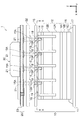
- the phototransistor array 10 includes a collector electrode 11, a collector layer 12, a base layer 13, an emitter layer 14, and an emitter electrode 15.
- the collector electrode 11 is a common electrode that extends in a plane along the XY plane shown in the figure, and the collector layer 12 is laminated on the collector electrode 11 directly or via another layer.
- a multilayer low resistance contact layer 16 is provided between the collector electrode 11 and the collector layer 12, and the collector electrode 11 and the low resistance contact layer 16 are connected via a solder layer 17.
- the low resistance contact layer 16 includes a Ti—Si layer 16A, an Al layer 16B, a Ni layer 16C, and the like appropriately stacked.
- the collector layer 12 has a common layer that supplies current to the collector electrode 11, and an upper portion thereof is divided by a mesa groove 18 to form a plurality of regions arranged in a plane.
- the collector layer 12 here is formed by laminating an n ⁇ layer 12B on an n + substrate 12A.
- a base layer 13 is laminated on the collector layer 12. Similarly to the upper part of the collector layer 12, the base layer 13 is divided into a plurality of planar areas by a mesa groove 18, and each of the divided areas includes a light receiving portion 13A.
- the emitter layer 14 is individually laminated on the divided base layer 13. Similarly to the upper part of the collector layer 12 and the base layer 13, the emitter layer 14 is also divided into a plurality of regions by mesa grooves 18. Further, in order to expose the light receiving portion 13A of the base layer 13, the emitter layer 14 is formed with a hole portion along the Z direction shown in the drawing corresponding to the light receiving portion 13A.
- Solder bumps 19 are respectively attached to the emitter layers 14 dispersed in a plurality of regions, and an emitter electrode 15 is connected to the emitter layer 14 via the solder bumps 19.
- the emitter electrode 15 is a common electrode for energizing all of the emitter layers 14 divided into a plurality of regions.
- the base layer 13 forms a p-layer bonded to the n ⁇ layer 12B of the collector layer 12, and the emitter layer 14 forms an n + layer bonded to the base layer 13, the mesa groove
- Each of the plurality of regions divided by 18 constitutes an npn-type bipolar transistor.
- the phototransistor array 10 is divided by the mesa groove 18 so that a plurality of electrically independent base layers 13 and emitter layers 14 are arranged along the XY plane.
- a common collector layer 12 is joined to 13 and the emitter layer 14.
- the light receiving element array 20 is disposed so as to face the base layer 13 and the emitter layer 14 of the phototransistor array 10.
- the light receiving element array 20 includes a plurality of light emitting elements 21, and the light emitting elements 21 are arranged in a plurality of regions of the base layer 13 into which the light emitting elements 21 are divided. The light emitted from the light emitting element 21 passes through the emitter electrode 15 and enters the light receiving portion 13A of the base layer 13.
- the emitter electrode 15 includes an opening 15A through which light emitted from the light emitting element 21 is transmitted.
- a microlens array 22 is disposed between the light emitting element array 20 and the phototransistor array 10 to collect the light emitted from the light emitting element 21 on the light receiving unit 13A.
- the light emitting element array 20 includes a substrate 23, and a plurality of light emitting elements 21 are arranged on the substrate 23.
- a drive IC serving as the control unit 30 is mounted on the substrate 23.
- the control unit 30 drives and controls the phototransistor array 10 by selectively causing the light emitting elements 21 to emit light.
- An emitter layer 14 is provided.
- the base layer 13 and the emitter layer 14 divided into 16 parts are defined as n1, n2,..., N15, and n16 areas.
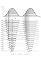
- the control unit 30 individually controls the light emission of the light emitting elements 21 corresponding to the n1, n2,..., N15, and n16 regions as shown in FIG.
- the control unit 30 controls blinking of each of the plurality of light emitting elements 21 at different light emission start timings and in the same cycle, and sequentially emits the plurality of light emitting elements 21 to the n1 region.
- the lighting time width is controlled to be sequentially shortened.
- light from the light emitting element 21 is irradiated in the order of the n1 region, the n2 region,..., The n15 region, and the n16 region.
- the first light emitting element 21 that irradiates the n1 region is turned on at the light emission start timing t1, and turned off after the lighting time width w1.
- the second light emitting element 21 that irradiates the n2 region is turned on at the light emission start timing t2, and turned off after the lighting time width w2.
- the fifteenth light emitting element 21 that irradiates the n15 region is turned on at the light emission start timing t15 and turned off after the lighting time width w15.
- the sixteenth light emitting element 21 that irradiates the n16 region is turned on at the light emission start timing t16 and turned off after the lighting time width w16.
- the light emission start timings t2,..., T16 are set within the time of (w1) / 2 from the light emission start timing t1, and the lighting time widths w1, w2,. ..., W15> w16.
- the flashing cycle Ts of each light emitting element 21 is such that the light emitting element 21 irradiating the n1 region is t1 to t17, the light emitting element 21 irradiating the n2 region is t2 to t18,.
- the light emitting elements 21 that irradiate the regions t31 and n16 are t16 to t32, and all have the same period.
- a power source is connected to the collector electrode 11 and an output current I 0 as shown in FIG. 5 can be obtained from the emitter electrode 15. That is, the emission start timing t1, t2 described above, ..., t15, t16 and lighting time width w1, w2, ..., w15, w16 is appropriately set it to, be from the output current I 0 is obtained an alternating current having a sine wave.
- inverter control for arbitrarily controlling the frequency of the alternating current is performed. Can do.
- the blinking cycle Ts of each light emitting element 21, that is, the drive cycle of each bipolar transistor divided into the n1, n2,..., N15, and n16 regions is a low frequency equal to the AC cycle obtained. Therefore, it is possible to perform desired inverter control even for a bipolar transistor in which a time delay occurs in turn-on and turn-off. In addition, since a high-frequency switching operation such as PWM or PFM is not performed, switching loss can be reduced by reducing the number of times of switching.
- the semiconductor device 1 having such a feature can eliminate a switching operation at a high frequency, even when used as a power device, generation of high-frequency high-power noise on the output side can be suppressed. As a result, stable control can be performed. Since a high-speed switching operation is not performed, it can be driven by a limited number of light-emitting elements, and a complicated structure and high cost can be avoided.
- the arrangement of the n1, n2,..., N15, and n16 regions shown in FIG. 2 can be arbitrarily changed by changing the order of the light emission start timing of each region.
- the influence of heat generation is reduced by arranging the younger order areas (n1, n2, n3, n4, etc.) having a long lighting time width apart from each other.
- the semiconductor device 1 As described above, according to the semiconductor device 1 according to the embodiment of the present invention, a power device capable of energy-saving operation with low noise can be realized.
Landscapes
- Engineering & Computer Science (AREA)
- Power Engineering (AREA)
- Photo Coupler, Interrupter, Optical-To-Optical Conversion Devices (AREA)
- Inverter Devices (AREA)
Abstract
インバータ制御を低周波数の駆動で実現することができ、ノイズの低減とスイッチング損失に伴うエネルギー損失の低減を図る。スイッチング制御がなされる複数の半導体スイッチング素子102の出力電圧を合成して出力波形を得るインバータ制御方法であって、各々の半導体スイッチング素子102の出力電圧は、一定周期で一定電圧レベルのパルス波形であり、全ての半導体スイッチング素子の出力電圧は、同一周期で同一電圧レベルであり異なるデューティ比を有し、パルス幅の中心タイミングが一致するように制御される。
Description
本発明は、インバータ制御方法、インバータ装置、半導体装置に関するものである。
電力の変換と制御の分野で用いられる半導体装置は、パワーデバイスと呼ばれており、整流ダイオード、パワートランジスタ(パワーMOSFET、絶縁ゲートバイポーラトランジスタ(IGBT))、サイリスタ、ゲートターンオフサイリスタ(GTO)などが一般に知られている。
モータなどの制御には、電源からの入力電力を所望の周波数の交流に変換して、その周波数を制御するインバータ方式が一般に採用されているが、インバータの制御は、IGBTやMOSFETなどをスイッチング動作させるパルス幅変調(PWM)やパルス周波数変調(PFM)が主流である。
パルス幅変調(PWM)やパルス周波数変調(PFM)によってインバータ制御を行うためには、IGBTやパワーMOSFETなどのスイッチング動作を高周波数で行うことが必要になる。このように、パワーデバイスを高周波数でスイッチング動作させると、出力側に高周波の大電流による高周波ノイズが発生することで制御信号にノイズがのり、安定した制御を行い難い問題がある。これに対しては、制御入力にフォトカプラや光FETを通してノイズを低減することが一般になされているが(下記特許文献1参照)、高速制御を行うには多くのフォトカプラや光FETを通して誘導ノイズを低減することが必要となり、構造が複雑化すると共に、高コストになる問題がある。
また、IGBTは、ターンオン或いはターンオフ時の過渡状態で生じるスイッチング損失が問題になる。パルス幅変調(PWM)やパルス周波数変調(PFM)によってインバータ制御を行うと、ターンオンとターンオフの繰り返し回数が必然的に多くなるので、スイッチング損失の蓄積によるエネルギー損失が無視できない問題になる。
本発明は、このような問題に対処することを課題の一例とするものである。すなわち、インバータ制御を低周波数の駆動で実現することができ、ノイズの低減とスイッチング損失に伴うエネルギー損失の低減を図ること、簡単な構造で低コストの半導体装置を得ること、などが本発明の目的である。
このような目的を達成するために、本発明のインバータ制御方法、インバータ装置、半導体装置は、以下の構成を具備するものである。
スイッチング制御がなされる複数の半導体スイッチング素子の出力電圧を合成して出力波形を得るインバータ制御方法であって、各々の前記半導体スイッチング素子の出力電圧は、一定周期で一定電圧レベルのパルス波形であり、全ての前記半導体スイッチング素子の出力電圧は、同一周期で同一電圧レベルであり異なるデューティ比を有し、パルス幅の中心タイミングが一致するように制御されることを特徴とするインバータ制御方法。
直流電源に対して並列接続される複数の半導体スイッチング素子と、前記複数の半導体スイッチング素子の出力電圧を制御する制御部とを備え、前記出力電圧を合成して出力波形を得るインバータ装置であって、前記制御部は、各々の前記出力電圧を、一定周期で一定電圧レベルのパルス波形とし、全ての前記出力波形を、同一周期で同一電圧レベルでありデューティ比が異なり、パルス幅の中心タイミングが一致するように制御することを特徴とするインバータ装置。
共通のコレクタ電極と、前記コレクタ電極上に直接又は他の層を介して積層され、前記コレクタ電極に通電する共通層を有するコレクタ層と、前記コレクタ層上に積層され、複数領域に分断されて、分断された各領域に受光部を備えるベース層と、分断された前記ベース層上に個別に積層されたエミッタ層と、前記エミッタ層に通電する共通のエミッタ電極とを備えるフォトトランジスタアレイと、前記エミッタ電極を透過して前記受光部に光を入射する発光素子を前記複数領域毎に配置した発光素子アレイと、前記発光素子を個別に制御する制御部とを備えることを特徴とする半導体装置。
このような特徴を有する本発明は、インバータ制御を低周波数の駆動で実現することができ、ノイズの低減とスイッチング損失に伴うエネルギー損失の低減を図ることができる。また、簡単な構造で低コストの半導体装置を得ることができる。
以下、図面を参照して本発明の実施形態を説明する。図1及び図2にて、本発明の実施形態に係るインバータ制御方法とインバータ装置を説明する。インバータ装置100は、直流電源101に対して並列接続される複数の半導体スイッチング素子102を備えるインバータ回路100Aと、複数の半導体スイッチング素子102の出力電圧を制御する制御部103を備えている。図示の例では、インバータ回路100Aは4個の半導体スイッチング素子102を備えているが、その数は特に限定されず、その数を増やすことによって、より正弦波に近い出力波形を得ることができる。
インバータ回路100Aの半導体スイッチング素子102は、図示の例ではIGBTであり、そのコレクタ-エミッタ間には還流ダイオード104が逆並列接続されている。また、それぞれの半導体スイッチング素子102の出力端子(エミッタ端子)には、調整抵抗105が直列接続されており、それぞれの調整抵抗105は、インバータ回路100Aの出力端子100Bに並列接続されている。半導体スイッチング素子102は、IGBTに限定されるものではなく、パワーMOSFETなど、スイッチング動作が可能なものであればよい。
制御部103は、半導体スイッチング素子102のゲート電圧を制御することで、各々の半導体スイッチング素子102をスイッチング制御する。制御部103によってスイッチング制御がなされる各々の半導体スイッチング素子102の出力電圧は、一定周期で一定電圧レベルのパルス波形(方形波)となり、この出力電圧が合成されて、インバータ回路100Aの出力波形が出力端子100Bから出力される。
図1に示す例では、インバータ装置100は、インバータ回路100Aの出力端子100Bに、共振コンデンサ111,112が一次側と二次側にそれぞれ並列接続された昇圧トランス110と、単相出力波形を3相出力波形に変換する相変換器120とを介して、負荷(モータなど)に接続されている。
図2に示したV1,V2,V3,V4は、制御部103によって制御される複数の半導体スイッチ102の各出力電圧を示している(縦軸Vが電圧で横軸tが時間)。出力電圧V1,V2,V3,V4は、それぞれが一定周期で一定電圧レベルのパルス波形であり、全ての出力電圧V1~V4は、同一の電圧レベルであって、同一周期Tで異なるデューティ比(異なるパルス幅)になっている。また、出力電圧V1~V4は、それぞれのパルス幅W1~W4の中心タイミングtsが一致するように制御されており、出力電圧V1~V4は、最大幅(W1)と最小幅(W4)の間で段階的に異なるパルス幅を有している。
このように出力電圧V1~V4を制御すると、インバータ回路100Aの出力端子100Bでは、出力電圧V1~V4のレベルを加算した階段状の出力波形Voを得る。ここで、半導体スイッチング素子102の数をNとすると、出力電圧V1~V4のパルス幅(W)をW=2W0・sin-1{(2n-1)/2N}(但し、W0は定数であり、nは1~Nの自然数の1つ)とすることで、正弦波に近い出力波形Voを得ることができる。N=4の場合には、出力電圧V1のパルス幅W1は、2W0・sin-1(1/8),出力電圧V2のパルス幅W2は、2W0・sin-1(3/8),出力電圧V3のパルス幅W3は、2W0・sin-1(5/8),出力電圧V4のパルス幅W4は、2W0・sin-1(7/8)となる。ここで、正弦波に近い出力波形にするには、半導体スイッチング素子102の数Nを増やせば良く、半導体スイッチング素子102のスイッチング周波数は変更する必要がない。
このようなインバータ装置100或いはこれによるインバータ制御方法によると、半導体スイッチング素子102のスイッチング動作は、出力波形の周波数と同等で良く、パルス幅変調(PWM)やパルス周波数変調(PFM)によってインバータ制御を行う場合のスイッチング動作と比べると低周波数の駆動になる。これよって、高周波数ノイズやスイッチング損失に伴うエネルギー損失を抑えたインバータ制御が可能になる。
図3及び図4は、前述したインバータ装置及びインバータ制御方法を実現するための半導体装置の構成例を示している。この半導体装置1は、フォトトランジスタアレイ10、発光素子アレイ20、制御部30を備えている。
フォトトランジスタアレイ10は、コレクタ電極11、コレクタ層12、ベース層13、エミッタ層14、エミッタ電極15を備えている。コレクタ電極11は、図示のX-Y平面に沿って平面的に拡がる共通の電極であり、コレクタ電極11上に、直接又は他の層を介してコレクタ層12が積層されている。図示の例では、コレクタ電極11とコレクタ層12との間には、多層の低抵抗接触層16を有し、コレクタ電極11と低抵抗接触層16とはハンダ層17を介して接続されている。低抵抗接触層16は、一例として、Ti-Si層16A、Al層16B、Ni層16Cなどが適宜積層されている。
コレクタ層12は、コレクタ電極11に通電する共通層を有しており、その上部は、メサ溝18によって分断されて、平面的に配置される複数領域が形成されている。ここでのコレクタ層12は、n+基板12A上にn-層12Bを積層して構成される。
コレクタ層12の上にはベース層13が積層されている。ベース層13は、コレクタ層12の上部と同様にメサ溝18によって、平面的な複数領域に分断されており、分断された複数領域の各領域は、受光部13Aを備えている。
分断されたベース層13の上には、個別にエミッタ層14が積層されている。このエミッタ層14も、コレクタ層12の上部及びベース層13と同様に、メサ溝18によって複数領域に分断されている。また、ベース層13の受光部13Aを露出させるために、エミッタ層14には、受光部13Aに対応して図示のZ方向に沿った孔部が形成されている。
複数領域に分散されているエミッタ層14にはそれぞれハンダバンプ19が付けられており、そのハンダバンプ19を介してエミッタ層14にエミッタ電極15が接続されている。エミッタ電極15は、複数領域に分断されたエミッタ層14の全てに通電する共通の電極である。
ここで、ベース層13は、コレクタ層12のn-層12Bに接合するp層を形成しており、エミッタ層14は、ベース層13に接合するn+層を形成しているので、メサ溝18によって分断された複数領域のそれぞれは、npn型のバイポーラトランジスタを構成している。
このように、フォトトランジスタアレイ10は、メサ溝18によって分断されることで電気的に独立したベース層13とエミッタ層14が、X-Y平面に沿って複数配列されており、これらのベース層13とエミッタ層14に共通のコレクタ層12が接合されている。
受光素子アレイ20は、フォトトランジスタアレイ10のベース層13とエミッタ層14に対向するように配置されている。受光素子アレイ20は、複数の発光素子21を備えており、この発光素子21が分割されたベース層13の複数領域毎に配置されている。発光素子21から出射した光は、エミッタ電極15を透過してベース層13の受光部13Aに入射する。
図示の例では、エミッタ電極15は、発光素子21が出射する光を透過する開口15Aを備えている。また、発光素子アレイ20とフォトトランジスタアレイ10との間には、発光素子21が出射した光を受光部13Aに集光するマイクロレンズアレイ22が配置されている。マイクロレンズアレイ22を設けることで、個々の発光素子21が出射した光をクロストーク無く、対向する受光部13Aに照射することができる。
発光素子アレイ20は、基板23を備えており、この基板23に複数の発光素子21が配置されている。また、基板23には、制御部30となるドライブICが実装されている。制御部30は、発光素子21を選択的に発光させることで、フォトトランジスタアレイ10を駆動制御するものである。
フォトトランジスタアレイ10は、図4に示すように、格子状のメサ溝18によって、X-Y平面にてn×m(図示の例では4×4=16)個に分断されたベース層13とエミッタ層14を備えている。図においては、16個に分断されたベース層13とエミッタ層14をn1領域,n2領域,…,n15領域,n16領域としている。
制御部30は、例えば、n1領域,n2領域,…,n15領域,n16領域に対応する発光素子21を図5に示すように個別に発光制御する。ここでは、制御部30は、複数の発光素子21のそれぞれを、異なる発光開始タイミングで且つ同周期で点滅制御し、複数の発光素子21を順次発光するに際して、n1領域に照射する第1番目の発光素子21の点灯時間幅内で、順次点灯時間幅が短くなるように制御する。
具体的には、n1領域,n2領域,…,n15領域,n16領域の順に発光素子21からの光が照射される。n1領域に照射する第1番目の発光素子21は、発光開始タイミングt1でONとなり、点灯時間幅w1後にOFFになる。n2領域に照射する第2番目の発光素子21は、発光開始タイミングt2でONとなり、点灯時間幅w2後にOFFになる。同様に、n15領域に照射する第15番目の発光素子21は、発光開始タイミングt15でONとなり、点灯時間幅w15後にOFFになる。n16領域に照射する第16番目の発光素子21は、発光開始タイミングt16でONとなり、点灯時間幅w16後にOFFになる。
ここで、発光開始タイミングt2,…,t16は、発光開始タイミングt1から(w1)/2の時間内に設定されており、点灯時間幅w1,w2,…,w15,w16は、w1>w2,…,w15>w16になるように設定されている。また、各発光素子21の点滅周期Tsは、n1領域に照射する発光素子21がt1~t17、n2領域に照射する発光素子21がt2~t18、…、n15領域に照射する発光素子21がt15~t31、n16領域に照射する発光素子21がt16~t32であって、全て同じ周期になっている。
制御部30がこのような発光制御を行うことで、コレクタ電極11に電源を接続して、エミッタ電極15から図5に示すような出力電流I0を得ることができる。すなわち、前述した発光開始タイミングt1,t2,…,t15,t16と点灯時間幅w1,w2,…,w15,w16を適宜設定することで、出力電流I0から正弦波の交流電流を得ることができ、また、発光開始タイミングt1,t2,…,t15,t16と点灯時間幅w1,w2,…,w15,w16を適宜制御することで、交流電流の周波数を任意に制御するインバータ制御を行うことができる。
この際、各発光素子21の点滅周期Ts、即ち、n1領域,n2領域,…,n15領域,n16領域に分断された各バイポーラトランジスタの駆動周期は、得られる交流の周期に等しい低周波数であるから、ターンオンとターンオフに時間遅れが生じるバイポーラトランジスタであっても所望のインバータ制御を行うことが可能になる。また、PWMやPFMのような高周波数のスイッチング動作を行わないので、スイッチング回数の減少によってスイッチング損失を低減することができる。
このような特徴の半導体装置1は、高周波数でのスイッチング動作を排除できるので、パワーデバイスとして使用する場合にも、出力側に大きなパワーの高周波数ノイズが発生するのを抑止することができ、これによって安定した制御を行うことができる。高速のスイッチング動作を行わないので、限られた個数の発光素子で駆動することができ、構造の複雑化や高コスト化を避けることができる。
なお、図2に示したn1領域,n2領域,…,n15領域,n16領域の配置は、各領域の発光開始タイミングの順番を換えて任意に変更することが可能である。図2に示した例では、点灯時間幅が長い若い順番の領域(n1領域,n2領域,n3領域,n4領域など)を周囲に離して配置することで、発熱の影響を少なくしている。この各領域と共に発光素子の発光開始順を随時変更することで、半導体装置1の発熱が一部に偏るのを避けることができる。
以上説明したように、本発明の実施形態に係る半導体装置1によると、低ノイズで省エネルギー動作が可能なパワーデバイスを実現することができる。
以上、本発明の実施の形態について図面を参照して詳述してきたが、具体的な構成はこれらの実施の形態に限られるものではなく、本発明の要旨を逸脱しない範囲の設計の変更等があっても本発明に含まれる。また、上述の各実施の形態は、その目的及び構成等に特に矛盾や問題がない限り、互いの技術を流用して組み合わせることが可能である。
100:インバータ装置,100A:インバータ回路,
100B:出力端子,101:直流電圧,102:半導体スイッチング素子,
103:制御部,104:還流ダイオード,105:調整抵抗,
110:昇圧トランス,111,112:共振コンデンサ,
120:相変換器,130:負荷(モータ),
1:半導体装置,10:フォトトランジスタアレイ,11:コレクタ電極,
12:コレクタ層,12A:n+基板,12B:n-層,
13:ベース層,13A:受光部,14:エミッタ層,
15:エミッタ電極,15A:開口,16:低抵抗接触層,
17:ハンダ層,18:メサ溝,19:ハンダバンプ,
20:発光素子アレイ,21:発光素子,22:マイクロレンズアレイ,
23:基板,30:制御部
100B:出力端子,101:直流電圧,102:半導体スイッチング素子,
103:制御部,104:還流ダイオード,105:調整抵抗,
110:昇圧トランス,111,112:共振コンデンサ,
120:相変換器,130:負荷(モータ),
1:半導体装置,10:フォトトランジスタアレイ,11:コレクタ電極,
12:コレクタ層,12A:n+基板,12B:n-層,
13:ベース層,13A:受光部,14:エミッタ層,
15:エミッタ電極,15A:開口,16:低抵抗接触層,
17:ハンダ層,18:メサ溝,19:ハンダバンプ,
20:発光素子アレイ,21:発光素子,22:マイクロレンズアレイ,
23:基板,30:制御部
Claims (12)
- スイッチング制御がなされる複数の半導体スイッチング素子の出力電圧を合成して出力波形を得るインバータ制御方法であって、
各々の前記半導体スイッチング素子の出力電圧は、一定周期で一定電圧レベルのパルス波形であり、
全ての前記半導体スイッチング素子の出力電圧は、同一周期で同一電圧レベルであり異なるデューティ比を有し、パルス幅の中心タイミングが一致するように制御されることを特徴とするインバータ制御方法。 - 複数の前記半導体スイッチング素子における出力電圧は、最大幅と最小幅の間で段階的に異なるパルス幅を有し、前記出力電圧のレベルを加算して前記出力波形を得ることを特徴とする請求項1記載のインバータ制御方法。
- 複数の前記半導体スイッチング素子の数をNとすると、
前記半導体スイッチング素子の出力電圧は、パルス幅(W)がW=2W0・sin-1{(2n-1)/2N}(但し、W0は定数であり、nは1~Nの自然数の1つ)であることを特徴とする請求項1又は2記載のインバータ制御方法。 - 直流電源に対して並列接続される複数の半導体スイッチング素子と、前記複数の半導体スイッチング素子の出力電圧を制御する制御部とを備え、前記出力電圧を合成して出力波形を得るインバータ装置であって、
前記制御部は、各々の前記出力電圧を、一定周期で一定電圧レベルのパルス波形とし、全ての前記出力波形を、同一周期で同一電圧レベルでありデューティ比が異なり、パルス幅の中心タイミングが一致するように制御することを特徴とするインバータ装置。 - 前記制御部は、複数の前記半導体スイッチング素子における出力電圧が、最大幅と最小幅の間で段階的に異なるパルス幅を有するように制御し、前記出力電圧のレベルを加算して前記出力波形を得ることを特徴とする請求項4記載のインバータ装置。
- 共通のコレクタ電極と、前記コレクタ電極上に直接又は他の層を介して積層され、前記コレクタ電極に通電する共通層を有するコレクタ層と、前記コレクタ層上に積層され、複数領域に分断されて、分断された各領域に受光部を備えるベース層と、分断された前記ベース層上に個別に積層されたエミッタ層と、前記エミッタ層に通電する共通のエミッタ電極とを備えるフォトトランジスタアレイと、
前記エミッタ電極を透過して前記受光部に光を入射する発光素子を前記複数領域毎に配置した発光素子アレイと、
前記発光素子を個別に制御する制御部とを備えることを特徴とする半導体装置。 - 前記エミッタ電極は、前記受光部に対応する開口部を有することを特徴とする請求項6記載の半導体装置。
- 前記コレクタ電極と前記コレクタ層との間には、多層の低抵抗接触層を有することを特徴とする請求項6又は7記載の半導体装置。
- 前記発光素子アレイと前記フォトトランジスタアレイとの間には、前記発光素子が出射した光を前記受光部に集光するマイクロレンズアレイが配置されることを特徴とする請求項6~8のいずれか1項記載の半導体装置。
- 前記制御部は、前記発光素子のそれぞれを、異なる発光開始タイミングで且つ同周期で点滅制御し、複数の前記発光素子を順次発光するに際して、第1番目の発光素子の点灯時間幅内で、順次点灯時間幅が短くなるように制御することを特徴とする請求項6~9のいずれか1項記載の半導体装置。
- 前記制御部は、前記発光素子の発光開始順を随時変更することを特徴とする請求項10記載の半導体装置。
- 前記複数領域は、格子状に形成されたメサ溝によって分断されていることを特徴とする請求項6~11のいずれか1項記載の半導体装置。
Applications Claiming Priority (2)
| Application Number | Priority Date | Filing Date | Title |
|---|---|---|---|
| JP2015098214A JP2018110139A (ja) | 2015-05-13 | 2015-05-13 | 半導体装置 |
| JP2015-098214 | 2015-05-13 |
Publications (1)
| Publication Number | Publication Date |
|---|---|
| WO2016182020A1 true WO2016182020A1 (ja) | 2016-11-17 |
Family
ID=57249164
Family Applications (1)
| Application Number | Title | Priority Date | Filing Date |
|---|---|---|---|
| PCT/JP2016/064140 Ceased WO2016182020A1 (ja) | 2015-05-13 | 2016-05-12 | インバータ制御方法、インバータ装置、半導体装置 |
Country Status (2)
| Country | Link |
|---|---|
| JP (1) | JP2018110139A (ja) |
| WO (1) | WO2016182020A1 (ja) |
Citations (6)
| Publication number | Priority date | Publication date | Assignee | Title |
|---|---|---|---|---|
| JPS5079246A (ja) * | 1973-11-12 | 1975-06-27 | ||
| JPS5694676A (en) * | 1979-12-12 | 1981-07-31 | Westinghouse Electric Corp | Optically responsive semiconductor device |
| JPH08181667A (ja) * | 1994-12-27 | 1996-07-12 | Fujitsu Ltd | 信号抽出方法およびそのための光半導体装置 |
| JP2000253675A (ja) * | 1999-03-04 | 2000-09-14 | Mitsubishi Electric Corp | 三相自励式電力変換装置および三相自励式直流連系装置 |
| JP2008546217A (ja) * | 2005-06-09 | 2008-12-18 | ヒューレット−パッカード デベロップメント カンパニー エル.ピー. | スーパーレンズ素子を用いて光学的に結合された集積回路層 |
| JP2012253862A (ja) * | 2011-06-01 | 2012-12-20 | Hitachi Ltd | 蓄電システム |
-
2015
- 2015-05-13 JP JP2015098214A patent/JP2018110139A/ja active Pending
-
2016
- 2016-05-12 WO PCT/JP2016/064140 patent/WO2016182020A1/ja not_active Ceased
Patent Citations (6)
| Publication number | Priority date | Publication date | Assignee | Title |
|---|---|---|---|---|
| JPS5079246A (ja) * | 1973-11-12 | 1975-06-27 | ||
| JPS5694676A (en) * | 1979-12-12 | 1981-07-31 | Westinghouse Electric Corp | Optically responsive semiconductor device |
| JPH08181667A (ja) * | 1994-12-27 | 1996-07-12 | Fujitsu Ltd | 信号抽出方法およびそのための光半導体装置 |
| JP2000253675A (ja) * | 1999-03-04 | 2000-09-14 | Mitsubishi Electric Corp | 三相自励式電力変換装置および三相自励式直流連系装置 |
| JP2008546217A (ja) * | 2005-06-09 | 2008-12-18 | ヒューレット−パッカード デベロップメント カンパニー エル.ピー. | スーパーレンズ素子を用いて光学的に結合された集積回路層 |
| JP2012253862A (ja) * | 2011-06-01 | 2012-12-20 | Hitachi Ltd | 蓄電システム |
Also Published As
| Publication number | Publication date |
|---|---|
| JP2018110139A (ja) | 2018-07-12 |
Similar Documents
| Publication | Publication Date | Title |
|---|---|---|
| CN100342632C (zh) | 功率变换器和用于功率变换的方法 | |
| US10381949B2 (en) | Power converter with reduced power loss | |
| JP6466392B2 (ja) | ハイブリッドコンバータシステム | |
| US10135360B2 (en) | Power converter | |
| CN107204708B (zh) | 一种用于有源开关器件的正负电源产生电路及方法 | |
| US20090296441A1 (en) | Semiconductor Power Switch | |
| WO2012176403A1 (ja) | 昇降圧型ac/dcコンバータ | |
| JP2017195691A (ja) | 電力変換装置 | |
| US10998827B2 (en) | Supply voltage connected p-type active clamp for switched mode power supply | |
| TW201230651A (en) | Inverter circuit, power converter circuit, and electric vehicle | |
| JP6012008B2 (ja) | スイッチング回路 | |
| JP6641782B2 (ja) | 電力変換装置 | |
| US20160241161A1 (en) | Converting circuit | |
| US9479049B2 (en) | Semiconductor module and boost rectifier circuit | |
| US20240322704A1 (en) | Ac-dc-ac converter for motor drive applications | |
| US12438474B2 (en) | AC-DC-AC converter for motor drive applications | |
| US11502612B2 (en) | Performance enhancement of silicon-based device | |
| JP2024086864A (ja) | スイッチングモジュール | |
| JP2021168534A (ja) | 電力変換装置 | |
| Sobe et al. | Experimental study of Si-and SiC-based voltage source inverters | |
| JP2009213307A (ja) | 電力変換装置 | |
| JP2018110139A (ja) | 半導体装置 | |
| US10998809B2 (en) | Power conversion apparatus | |
| JP2664163B2 (ja) | 高周波pwmフルブリッジ電力変換装置 | |
| Nguyen et al. | Compact, isolated and simple to implement gate driver using high frequency transformer |
Legal Events
| Date | Code | Title | Description |
|---|---|---|---|
| 121 | Ep: the epo has been informed by wipo that ep was designated in this application |
Ref document number: 16792745 Country of ref document: EP Kind code of ref document: A1 |
|
| NENP | Non-entry into the national phase |
Ref country code: DE |
|
| 122 | Ep: pct application non-entry in european phase |
Ref document number: 16792745 Country of ref document: EP Kind code of ref document: A1 |
|
| NENP | Non-entry into the national phase |
Ref country code: JP |