WO2016181757A1 - 表示装置、表示方法、および電子機器 - Google Patents
表示装置、表示方法、および電子機器 Download PDFInfo
- Publication number
- WO2016181757A1 WO2016181757A1 PCT/JP2016/062087 JP2016062087W WO2016181757A1 WO 2016181757 A1 WO2016181757 A1 WO 2016181757A1 JP 2016062087 W JP2016062087 W JP 2016062087W WO 2016181757 A1 WO2016181757 A1 WO 2016181757A1
- Authority
- WO
- WIPO (PCT)
- Prior art keywords
- luminance information
- unit
- display
- correction
- display device
- Prior art date
- Legal status (The legal status is an assumption and is not a legal conclusion. Google has not performed a legal analysis and makes no representation as to the accuracy of the status listed.)
- Ceased
Links
Images




Classifications
-
- G—PHYSICS
- G02—OPTICS
- G02F—OPTICAL DEVICES OR ARRANGEMENTS FOR THE CONTROL OF LIGHT BY MODIFICATION OF THE OPTICAL PROPERTIES OF THE MEDIA OF THE ELEMENTS INVOLVED THEREIN; NON-LINEAR OPTICS; FREQUENCY-CHANGING OF LIGHT; OPTICAL LOGIC ELEMENTS; OPTICAL ANALOGUE/DIGITAL CONVERTERS
- G02F1/00—Devices or arrangements for the control of the intensity, colour, phase, polarisation or direction of light arriving from an independent light source, e.g. switching, gating or modulating; Non-linear optics
- G02F1/01—Devices or arrangements for the control of the intensity, colour, phase, polarisation or direction of light arriving from an independent light source, e.g. switching, gating or modulating; Non-linear optics for the control of the intensity, phase, polarisation or colour
- G02F1/13—Devices or arrangements for the control of the intensity, colour, phase, polarisation or direction of light arriving from an independent light source, e.g. switching, gating or modulating; Non-linear optics for the control of the intensity, phase, polarisation or colour based on liquid crystals, e.g. single liquid crystal display cells
- G02F1/133—Constructional arrangements; Operation of liquid crystal cells; Circuit arrangements
-
- G—PHYSICS
- G09—EDUCATION; CRYPTOGRAPHY; DISPLAY; ADVERTISING; SEALS
- G09G—ARRANGEMENTS OR CIRCUITS FOR CONTROL OF INDICATING DEVICES USING STATIC MEANS TO PRESENT VARIABLE INFORMATION
- G09G3/00—Control arrangements or circuits, of interest only in connection with visual indicators other than cathode-ray tubes
- G09G3/20—Control arrangements or circuits, of interest only in connection with visual indicators other than cathode-ray tubes for presentation of an assembly of a number of characters, e.g. a page, by composing the assembly by combination of individual elements arranged in a matrix no fixed position being assigned to or needed to be assigned to the individual characters or partial characters
- G09G3/34—Control arrangements or circuits, of interest only in connection with visual indicators other than cathode-ray tubes for presentation of an assembly of a number of characters, e.g. a page, by composing the assembly by combination of individual elements arranged in a matrix no fixed position being assigned to or needed to be assigned to the individual characters or partial characters by control of light from an independent source
- G09G3/3406—Control of illumination source
-
- G—PHYSICS
- G09—EDUCATION; CRYPTOGRAPHY; DISPLAY; ADVERTISING; SEALS
- G09G—ARRANGEMENTS OR CIRCUITS FOR CONTROL OF INDICATING DEVICES USING STATIC MEANS TO PRESENT VARIABLE INFORMATION
- G09G3/00—Control arrangements or circuits, of interest only in connection with visual indicators other than cathode-ray tubes
- G09G3/20—Control arrangements or circuits, of interest only in connection with visual indicators other than cathode-ray tubes for presentation of an assembly of a number of characters, e.g. a page, by composing the assembly by combination of individual elements arranged in a matrix no fixed position being assigned to or needed to be assigned to the individual characters or partial characters
-
- G—PHYSICS
- G09—EDUCATION; CRYPTOGRAPHY; DISPLAY; ADVERTISING; SEALS
- G09G—ARRANGEMENTS OR CIRCUITS FOR CONTROL OF INDICATING DEVICES USING STATIC MEANS TO PRESENT VARIABLE INFORMATION
- G09G3/00—Control arrangements or circuits, of interest only in connection with visual indicators other than cathode-ray tubes
- G09G3/20—Control arrangements or circuits, of interest only in connection with visual indicators other than cathode-ray tubes for presentation of an assembly of a number of characters, e.g. a page, by composing the assembly by combination of individual elements arranged in a matrix no fixed position being assigned to or needed to be assigned to the individual characters or partial characters
- G09G3/22—Control arrangements or circuits, of interest only in connection with visual indicators other than cathode-ray tubes for presentation of an assembly of a number of characters, e.g. a page, by composing the assembly by combination of individual elements arranged in a matrix no fixed position being assigned to or needed to be assigned to the individual characters or partial characters using controlled light sources
- G09G3/30—Control arrangements or circuits, of interest only in connection with visual indicators other than cathode-ray tubes for presentation of an assembly of a number of characters, e.g. a page, by composing the assembly by combination of individual elements arranged in a matrix no fixed position being assigned to or needed to be assigned to the individual characters or partial characters using controlled light sources using electroluminescent panels
-
- G—PHYSICS
- G09—EDUCATION; CRYPTOGRAPHY; DISPLAY; ADVERTISING; SEALS
- G09G—ARRANGEMENTS OR CIRCUITS FOR CONTROL OF INDICATING DEVICES USING STATIC MEANS TO PRESENT VARIABLE INFORMATION
- G09G3/00—Control arrangements or circuits, of interest only in connection with visual indicators other than cathode-ray tubes
- G09G3/20—Control arrangements or circuits, of interest only in connection with visual indicators other than cathode-ray tubes for presentation of an assembly of a number of characters, e.g. a page, by composing the assembly by combination of individual elements arranged in a matrix no fixed position being assigned to or needed to be assigned to the individual characters or partial characters
- G09G3/34—Control arrangements or circuits, of interest only in connection with visual indicators other than cathode-ray tubes for presentation of an assembly of a number of characters, e.g. a page, by composing the assembly by combination of individual elements arranged in a matrix no fixed position being assigned to or needed to be assigned to the individual characters or partial characters by control of light from an independent source
-
- G—PHYSICS
- G09—EDUCATION; CRYPTOGRAPHY; DISPLAY; ADVERTISING; SEALS
- G09G—ARRANGEMENTS OR CIRCUITS FOR CONTROL OF INDICATING DEVICES USING STATIC MEANS TO PRESENT VARIABLE INFORMATION
- G09G3/00—Control arrangements or circuits, of interest only in connection with visual indicators other than cathode-ray tubes
- G09G3/20—Control arrangements or circuits, of interest only in connection with visual indicators other than cathode-ray tubes for presentation of an assembly of a number of characters, e.g. a page, by composing the assembly by combination of individual elements arranged in a matrix no fixed position being assigned to or needed to be assigned to the individual characters or partial characters
- G09G3/34—Control arrangements or circuits, of interest only in connection with visual indicators other than cathode-ray tubes for presentation of an assembly of a number of characters, e.g. a page, by composing the assembly by combination of individual elements arranged in a matrix no fixed position being assigned to or needed to be assigned to the individual characters or partial characters by control of light from an independent source
- G09G3/36—Control arrangements or circuits, of interest only in connection with visual indicators other than cathode-ray tubes for presentation of an assembly of a number of characters, e.g. a page, by composing the assembly by combination of individual elements arranged in a matrix no fixed position being assigned to or needed to be assigned to the individual characters or partial characters by control of light from an independent source using liquid crystals
Definitions
- the present disclosure relates to a display device that displays an image, a display method used in such a display device, and an electronic device including such a display device.
- Patent Document 1 discloses a display device that expands a dynamic range in gradation display by changing both a current flowing through a light emitting element and a light emission time of the light emitting element.
- Patent Document 2 discloses a display device including a liquid crystal panel and a backlight that emits light with a light emission amount corresponding to the maximum value and the minimum value of the pixel values in the frame.
- the display device is desired to have high image quality, and further improvement in image quality is expected.
- the display device includes a correction unit and a display unit.
- the correction unit has a plurality of correction tables, selects one of the plurality of correction tables based on the first luminance information, and performs a correction operation on the first luminance information using the selected correction table. To generate second luminance information.
- the display unit performs display based on the second luminance information.
- a display method selects one of a plurality of correction tables based on first luminance information, and performs a correction operation on the first luminance information using the selected correction table. To generate second luminance information and display based on the second luminance information.
- An electronic device includes the display device, and includes, for example, a television device, an electronic book, a smartphone, a digital camera, a notebook personal computer, a video camera, a head mounted display, and the like. To do.
- the correction calculation is performed on the first luminance information to generate the second correction information, and the second luminance information A display is performed based on this.
- one of the plurality of correction tables is selected based on the first luminance information, and the second luminance information is generated using the selected correction table.
- one of the plurality of correction tables is selected based on the first luminance information, and the first correction table is used to select the first correction table. Since the correction calculation is performed on the luminance information of 1, the image quality can be improved.
- the effect described here is not necessarily limited, and there may be any effect described in the present disclosure.
- FIG. 3 is a block diagram illustrating a configuration example of a display device according to a first embodiment of the present disclosure.
- FIG. FIG. 2 is a block diagram illustrating a configuration example of an image processing unit illustrated in FIG. 1.
- FIG. 3 is an explanatory diagram illustrating an operation example of the image processing unit illustrated in FIG. 2.
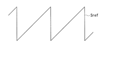
- It is a wave form diagram showing an example of the reference signal shown in FIG.
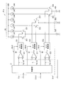
- FIG. 2 is a block diagram illustrating a configuration example of a pixel illustrated in FIG. 1.
- FIG. 6 is a timing waveform diagram illustrating an operation example of the drive unit illustrated in FIG. 5.
- FIG. 6 is a timing waveform diagram illustrating an operation example of the drive unit illustrated in FIG. 5.
- It is a block diagram showing the example of 1 structure of the display apparatus which concerns on 2nd Embodiment. It is a perspective view showing the external appearance structure of the example of application of the display apparatus which concerns on embodiment.
- FIG. 1 illustrates a configuration example of the display device (display device 1) according to the first embodiment.
- the display device 1 uses an LED (Light Emitting Diode) as a display element.
- the display method according to the embodiment of the present disclosure is embodied by the present embodiment, and will be described together.
- the display device 1 includes an image processing unit 20, a timing control unit 11, a display drive unit 12, and a display unit 13.
- the display device 1 displays an image based on the image signal Spic.
- the image signal Spic includes luminance information INFR, INFG, and INFB.
- the luminance information INFR indicates the luminance value of red (R)
- the luminance information INFG indicates the luminance value of green (G)
- the luminance information INFB indicates the luminance value of blue (B).
- the luminance information INFR, INFG, and INFB each have a value that is greater than or equal to 0 and less than or equal to the value INFmax.
- the luminance information INF is appropriately used to represent any one of the luminance information INFR, INFG, and INFB.
- the image processing unit 20 generates the image signal Spic3 and the control signal Sctrl based on the image signal Spic.
- FIG. 2 shows a configuration example of the image processing unit 20.
- the image processing unit 20 includes a control signal generation unit 21, a correction unit 22, and a calculation unit 23.
- the control signal generator 21 generates the control signal Sctrl based on the image signal Spic. Specifically, the control signal generator 21 compares the value of the luminance information INF included in the image signal Spic with a predetermined threshold value INFth. Then, when the value of the luminance information INF is larger than the threshold value INFth, the control signal generation unit 21 generates the control signal Sctrl whose value is “1”, and the value of the luminance information INF is the threshold value INFth. In the following cases, the control signal Sctrl having a value of “0” is generated.
- the correction unit 22 generates luminance information INF2 (INFR2, INFG2, INFB2) by correcting the luminance information INF (INFR, INFG, INFB) included in the image signal Spic based on the control signal Sctrl. .
- the correction unit 22 has correction tables T1 and T2.
- the correction tables T1 and T2 are for correcting characteristic variations of a light emitting element 40 (described later) in the display unit 13 and correcting a chromaticity change of the light emitting element 40 due to a drive current.
- Each of the correction tables T1 and T2 includes a number of correction data D corresponding to the number of light emitting elements 40 in the display unit 13.
- the correction table T1 is used when the value of the luminance information INF is larger than the threshold value INFth
- the correction table T2 is used when the value of the luminance information INF is less than or equal to the threshold value INFth.
- the correction unit 22 first selects a correction table to be used from the correction tables T1 and T2 based on the control signal Sctrl. Specifically, when the value of the control signal Sctrl is “1”, the correction table T1 is selected, and when the value of the control signal Sctrl is “0”, the correction table T2 is selected. Then, the correction unit 22 generates the luminance information INF2 by correcting the luminance information INF based on the correction data D included in the selected correction table. The correcting unit 22 outputs the luminance information INF2 as an image signal Spic2.
- the calculation unit 23 generates luminance information INF3 (INFR3, INFG3, INFB3) by calculating the luminance information INF2 (INFR2, INFG2, INFB2) included in the image signal Spic2 based on the control signal Sctrl. Is. Specifically, when the value of the control signal Sctrl is “1”, the calculation unit 23 generates the luminance information INF3 by multiplying the value of the luminance information INF2 by the gain G1. The gain G1 is “1” in this example. In addition, when the value of the control signal Sctrl is “0”, the arithmetic unit 23 generates the luminance information INF3 by multiplying the value of the luminance information INF2 by the gain G2. The gain G2 is “20” in this example. And the calculating part 23 outputs the luminance information INF3 as an image signal Spic3.
- FIG. 3 shows an operation example of the calculation unit 23.
- the correction unit 22 does not correct the luminance information INF and outputs the luminance information INF as luminance information INF2 for convenience of explanation.
- the value of the luminance information INF is larger than the threshold value INFth
- the value of the luminance information INF3 output from the calculation unit 23 is the same as the value of the luminance information INF2.
- the value of the luminance information INF is less than or equal to the threshold value INFth
- the value of the luminance information INF3 is 20 times the value of the luminance information INF2 in this example.
- the calculation unit 23 increases the value of the luminance information INF3 by using the high gain G2 when the value of the luminance information INF is low.
- the display device 1 is configured to reduce the possibility that the image quality is lowered when the value of the luminance information INF is low.
- the timing control unit 11 (FIG. 1) controls the display drive unit 12 and the display unit 13 to operate in synchronization with each other based on the image signal Spic. Specifically, the timing control unit 11 supplies a control signal to the display driving unit 12 and supplies a reference signal Sref to the display unit 13.
- FIG. 4 shows an example of the waveform of the reference signal Sref.
- the reference signal Sref has a so-called sawtooth waveform.
- the timing control unit 11 generates a reference signal Sref having such a waveform and supplies it to the display unit 13.
- the display driving unit 12 generates a pixel signal Sig based on the image signal Spic3 and the control signal supplied from the timing control unit 11, and supplies the pixel signal Sig to the display unit 13.
- the display unit 13 displays an image based on the pixel signal Sig, the control signal Sctrl, and the reference signal Sref.
- the display unit 13 has a plurality of pixels Pix arranged in a matrix.
- FIG. 5 shows a configuration example of the pixel Pix.
- the pixel Pix has a drive unit 30 and three light emitting elements 40 (40R, 40G, 40B).
- the driving unit 30 supplies driving currents to the light emitting elements 40R, 40G, and 40B based on the pixel signal Sig, the control signal Sctrl, and the reference signal Sref, respectively.
- the drive unit 30 includes a control unit 31, comparators 321 to 323, switch control units 331 to 333, current sources 341 to 346, and switches 351 to 356.
- the control unit 31 generates pixel voltages VpixR, VpixG, VpixG and switch control signals SELR, SELG, SELB based on the pixel signal Sig and the control signal Sctrl. Specifically, the control unit 31 performs D / A (Digital / Analog) conversion based on the luminance information INFR3, INFG3, INFB3 of the pixel Pix included in the pixel signal Sig, so that the pixel voltage VpixR, VpixG and VpixB are generated respectively. Further, the control unit 31 generates switch control signals SELR, SELG, and SELB based on the control signal Sctrl.
- D / A Digital / Analog
- control unit 31 outputs the control signal Sctrl corresponding to the luminance information INFR3 of the pixel Pix as the switch control signal SELR, and the control signal Sctrl corresponding to the luminance information INFG3 of the pixel Pix is output as the switch control signal SELG.
- the control signal Sctrl corresponding to the luminance information INFB3 of the pixel Pix is output as the switch control signal SELB.
- the comparator 321 generates the pulse signal SR by comparing the pixel voltage VpixR with the reference signal Sref.
- the comparator 322 generates the pulse signal SG by comparing the pixel voltage VpixG with the reference signal Sref.
- the comparator 323 generates the pulse signal SB by comparing the pixel voltage VpixB with the reference signal Sref.
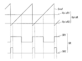
- FIG. 6 shows an operation example of the comparator 321.
- the comparator 321 generates the pulse signal SR by comparing the pixel voltage VpixR with the reference signal Sref. For example, when the pixel voltage VpixR is medium (pixel voltage VpixR1), the duty ratio of the pulse signal SR (pulse signal SR1) is about 50%. For example, when the pixel voltage VpixR is low (pixel voltage VpixR2), the duty ratio of the pulse signal SR (pulse signal SR2) is small. Thus, the comparator 321 generates the pulse signal SR having a pulse width corresponding to the pixel voltage VpixR.
- the switch control unit 331 (FIG. 5) controls the switches 351 and 352 based on the switch control signal SELR and the pulse signal SR. Specifically, when the switch control signal SELR is “1”, the switch control unit 331 performs on / off control of the switch 351 based on the pulse signal SR and maintains the switch 352 in the off state. Further, when the switch control signal SELR is “0”, the switch control unit 331 controls the switch 352 on and off based on the pulse signal SR and maintains the switch 351 in the off state.
- the switch control unit 332 controls the switches 353 and 354 based on the switch control signal SELG and the pulse signal SG. Specifically, when the switch control signal SELG is “1”, the switch control unit 332 controls on / off of the switch 353 based on the pulse signal SG and maintains the switch 354 in the off state. Further, when the switch control signal SELG is “0”, the switch control unit 332 controls on / off of the switch 354 based on the pulse signal SG and maintains the switch 353 in the off state.
- the switch control unit 333 controls the switches 355 and 356 based on the switch control signal SELB and the pulse signal SB. Specifically, when the switch control signal SELB is “1”, the switch control unit 333 controls on / off of the switch 355 based on the pulse signal SB and maintains the switch 356 in the off state. Further, when the switch control signal SELB is “0”, the switch control unit 333 controls on / off of the switch 356 based on the pulse signal SB and maintains the switch 355 in the off state.
- the current sources 341, 343, and 345 flow a predetermined drive current I1 from one end to the other end.
- the current sources 342, 344, and 346 flow a predetermined drive current I2 from one end to the other end.
- the value of the drive current I1 is, for example, 100 [ ⁇ A]
- the value of the drive current I2 is, for example, 5 [ ⁇ A]. That is, in this example, the current value of the drive current I2 is “1/20” of the drive current I1.
- the power source voltage VDD is applied to one end of the current source 341, and the other end is connected to one end of the switch 351.
- the power source voltage VDD is applied to one end of the current source 342, and the other end is connected to one end of the switch 352.
- the power source voltage VDD is applied to one end of the current source 343, and the other end is connected to one end of the switch 353.
- the power supply voltage VDD is applied to one end of the current source 344, and the other end is connected to one end of the switch 354.
- the power source voltage VDD is applied to one end of the current source 345, and the other end is connected to one end of the switch 355.
- the power source voltage VDD is applied to one end of the current source 346, and the other end is connected to one end of the switch 356.
- the switch 351 turns on and off between one end and the other end based on a control signal supplied from the switch control unit 331, one end is connected to the other end of the current source 341, and the other end is other than the switch 352. It is connected to the end and connected to the anode of the light emitting element 40R.
- the switch 352 turns on and off between one end and the other end based on a control signal supplied from the switch control unit 331, one end is connected to the other end of the current source 342, and the other end is the other of the switch 351. It is connected to the end and connected to the anode of the light emitting element 40R.
- the switch 353 turns on / off between one end and the other end based on a control signal supplied from the switch control unit 332, one end is connected to the other end of the current source 343, and the other end is the other switch. It is connected to the end and connected to the anode of the light emitting element 40G.
- the switch 354 turns on and off between one end and the other end based on a control signal supplied from the switch control unit 332, one end is connected to the other end of the current source 344, and the other end is the other switch 353. It is connected to the end and connected to the anode of the light emitting element 40G.
- the switch 355 turns on and off between one end and the other end based on a control signal supplied from the switch control unit 333, one end is connected to the other end of the current source 345, and the other end is the other of the switch 356. It is connected to the end and connected to the anode of the light emitting element 40B.
- the switch 356 turns on and off between one end and the other end based on a control signal supplied from the switch control unit 333, one end is connected to the other end of the current source 346, and the other end is the other of the switch 355. It is connected to the end and connected to the anode of the light emitting element 40B.
- the light emitting elements 40R, 40G, and 40B are configured using, for example, LEDs, and emit light based on the supplied drive current.
- the light emitting element 40R emits red (R) light
- the anode is connected to the other end of the switch 351 and the other end of the switch 352, and the cathode is grounded.
- the light emitting element 40G emits green (G) light
- the anode is connected to the other end of the switch 353 and the other end of the switch 354, and the cathode is grounded.
- the light emitting element 40B emits blue (B) light.
- the anode is connected to the other end of the switch 355 and the other end of the switch 356, and the cathode is grounded.
- the driving unit 30 supplies a driving current to the light emitting element 40R in a period having a length corresponding to the pixel voltage VpixR.
- the drive unit 30 selects one of the current sources 341 and 342 according to the switch control signal SELR, and the selected current source supplies the drive current to the light emitting element 40R.
- the light emitting element 40R emits light with a luminance corresponding to the drive current in a period of a length corresponding to the pixel voltage VpixR.
- the drive unit 30 supplies a drive current having a current value corresponding to the switch control signal SELG to the light emitting element 40G in a period corresponding to the pixel voltage VpixG.
- the light emitting element 40G emits light with a luminance corresponding to the drive current in a period corresponding to the pixel voltage VpixG.
- the driving unit 30 supplies a driving current having a current value corresponding to the switch control signal SELB to the light emitting element 40G in a period corresponding to the pixel voltage VpixB.
- the light emitting element 40B emits light with a luminance corresponding to the driving current in a period of a length corresponding to the pixel voltage VpixB.
- the luminance information INF corresponds to a specific example of “first luminance information” in the present disclosure.
- the luminance information INF2 corresponds to a specific example of “second luminance information” in the present disclosure.
- the luminance information INF3 corresponds to a specific example of “third luminance information” in the present disclosure.
- the timing control unit 11 corresponds to a specific example of a “signal generation unit” in the present disclosure.
- the image processing unit 20 (FIG. 1) generates an image signal Spic3 and a control signal Sctrl based on the image signal Spic.
- the control signal generation unit 21 (FIG. 2) generates the control signal Sctrl based on the image signal Spic.
- the correction unit 22 corrects the luminance information INF (INFR, INFG, INFB) included in the image signal Spic by using the correction table corresponding to the control signal Sctrl in the correction tables T1 and T2, thereby correcting the luminance information INF2 (INFR2, INFG2, INFB2) is generated.
- the computing unit 23 generates the luminance information INF3 (INFR3, INFG3, INFB3) by multiplying the value of the luminance information INF2 by a gain corresponding to the control signal Sctrl among the gains G1, G2. Then, the calculation unit 23 outputs the luminance information INF3 as an image signal Spic3.
- the timing control unit 11 (FIG. 1) supplies a control signal to the display driving unit 12 and supplies a reference signal Sref to the display unit 13.
- the display driver 12 generates a pixel signal Sig based on the image signal Spic3.
- the display unit 13 displays an image based on the pixel signal Sig, the control signal Sctrl, and the reference signal Sref.
- the control unit 31 (FIG. 5) of the pixel Pix generates the pixel voltages VpixR, VpixG, VpixG and the switch control signals SELR, SELG, SELB based on the pixel signal Sig and the control signal Sctrl.
- the comparator 321 generates the pulse signal SR by comparing the pixel voltage VpixR with the reference signal Sref.
- the switch control unit 331 controls the switches 351 and 352 based on the switch control signal SELR and the pulse signal SR.
- the light emitting element 40R emits light based on the drive current supplied from the current sources 341 and 342.
- the comparator 322 generates the pulse signal SG by comparing the pixel voltage VpixG with the reference signal Sref.
- the switch control unit 332 controls the switches 353 and 354 based on the switch control signal SELG and the pulse signal SG.
- the light emitting element 40G emits light based on the drive current supplied from the current sources 343 and 344.
- the comparator 323 generates the pulse signal SB by comparing the pixel voltage VpixB with the reference signal Sref.
- the switch control unit 333 controls the switches 355 and 356 based on the switch control signal SELB and the pulse signal SB.
- the light emitting element 40B emits light based on the drive current supplied from the current sources 345 and 346.
- the correction tables T1 and T2, the gains G1 and G2, and the drive currents I1 and I2 are switched according to the value of the luminance information INF.
- the display device 1 uses the correction table T1, the gain G1, and the drive current I1 when the value of the luminance information INF is larger than the threshold value INFth.
- the gain G1 is, for example, “1”
- the driving current I1 is, for example, 100 [ ⁇ A].
- the display device 1 uses the correction table T2, the gain G2, and the drive current I2 when the value of the luminance information INF is equal to or less than the threshold value INFth.
- the gain G2 is “20”, for example, and the drive current I2 is 5 [ ⁇ A], for example.
- the display device 1 when the value of the luminance information INF is larger than the threshold value INFth, the display device 1 reduces the gain and increases the drive current, and when the luminance information INF value is equal to or smaller than the threshold value INFth. Increases the gain and decreases the drive current. As a result, the display device 1 can reduce the possibility that the image quality will deteriorate when the value of the luminance information INF is low, as will be described below.
- FIG. 7 shows the waveform of the pulse signal SR when the value of the luminance information INFR is low.
- the pixel voltage VpixR is also low.
- the duty ratio of the pulse signal SR becomes small.
- the reference signal Sref has a so-called sawtooth waveform. Therefore, for example, the waveform of the portion W shown in FIG. 7 may be lost due to the influence of parasitic resistance and parasitic capacitance. When a part of the waveform is lost in this way, the duty ratio of the pulse signal SR deviates from an ideal duty ratio corresponding to the pixel voltage VpixR, and as a result, the image quality may be deteriorated. .
- the luminance information INF3 is generated by multiplying the luminance information INF2 by a large gain G2.
- the pixel voltage VpixR is high, so even when the value of the luminance information INFR is low, the opportunity to use the portion W shown in FIG. 7 is reduced.
- the possibility that the duty ratio of the pulse signal SR deviates from an ideal duty ratio corresponding to the pixel voltage VpixR can be reduced, and the image quality can be improved.
- the correction tables T1 and T2 are switched according to the value of the luminance information INF, so that the image quality can be improved. That is, first, in the display device 1, the drive currents I1 and I2 are switched according to the switching of the gains G1 and G2. In general, when the driving current changes, the light emitting element not only changes in luminance but also may change in chromaticity. In the display device 1, since the drive currents I1 and I2 are switched according to the value of the luminance information INF and the correction tables T1 and T2 are switched, the change in chromaticity can be corrected according to the drive current. Therefore, the image quality can be improved.
- the gain and the drive current are switched in accordance with the value of the luminance information, so that the image quality can be improved.
- the correction table is switched according to the value of the luminance information, the chromaticity can be corrected, so that the image quality can be improved.
- the light emitting element 40 was comprised using LED, it is not limited to this, For example, you may comprise using a laser diode, an EL (Electro Luminescence) element, etc.
- the two correction tables T1 and T2 are provided.
- the present invention is not limited to this.
- three or more correction tables may be provided. Specifically, for example, according to the value of the luminance information INF, one of the three correction tables is selected, one of the three gains is selected, and one of the three drive currents is selected. May be selected.
- FIG. 8 shows a configuration example of the display device 2.
- the display device 2 includes an image processing unit 50, a timing control unit 41, a display driving unit 42, a scanning unit 43, a liquid crystal display unit 44, and a backlight 45.
- the image processing unit 50 includes a control signal generation unit 51 as shown in FIG.
- the control signal generator 51 obtains an average value AVG of the luminance information INF for one frame based on the image signal Spic, and compares the average value AVG with a predetermined threshold value INFth to thereby obtain a control signal Sctrl. Is generated. Specifically, when the average value AVG is larger than the threshold value INFth, the control signal generation unit 51 generates the control signal Sctrl whose value is “1”, and the average value AVG is equal to or less than the threshold value INFth. In this case, the control signal Sctrl having a value “0” is generated.
- the timing control unit 41 supplies control signals to the display driving unit 42 and the scanning unit 43 based on the image signal Spic so that the display driving unit 42 and the scanning unit 43 operate in synchronization with each other. To control.
- the display drive unit 42 generates a pixel voltage Vpix by performing D / A conversion on the luminance information INF3 based on the image signal Spic3 and the control signal supplied from the timing control unit 41.
- the display driver 42 outputs the pixel voltage Vpix as the pixel signal Sig2.
- the scanning unit 32 generates a scanning signal Scan for selecting a pixel Pix2 (described later) of the liquid crystal display unit 44 in units of lines based on the control signal supplied from the timing control unit 41.
- the liquid crystal display unit 44 displays an image based on the pixel signal Sig2 and the scanning signal Scan.
- the liquid crystal display unit 44 has a plurality of pixels Pix2 arranged in a matrix.
- the pixel Pix2 includes a sub-pixel that transmits red light, a sub-pixel that transmits green light, and a sub-pixel that transmits blue light. Each sub-pixel changes the transmittance of the light emitted from the backlight 45 based on the pixel voltage Vpix.
- the backlight 45 emits white light to the liquid crystal display unit 44.
- the backlight 45 includes, for example, an LED that emits red light, an LED that emits green light, and an LED that emits blue light, and emits white light in which these lights are mixed.
- the backlight 45 is configured to change the light emission luminance based on the control signal Sctrl. Specifically, the drive current I1 or the drive current I2 is supplied to these LEDs based on the control signal Sctrl.
- the correction tables T1, T2, the gains G1, G2, and the drive currents I1, I2 are switched according to the value of the luminance information INF, similarly to the display device 1 according to the above embodiment. That is, in the display device 2, when the value of the luminance information INF is larger than the threshold value INFth, the gain is decreased and the driving current is increased, and when the value of the luminance information INF is equal to or smaller than the threshold value INFth. Increases the gain and decreases the drive current. At that time, the display device 2 switches the correction tables T1 and T2 in accordance with the drive currents I1 and I2, so that the image quality can be improved.
- each LED of the backlight 45 may change not only in luminance but also in chromaticity when the drive current changes.
- the drive currents I1 and I2 are switched according to the value of the luminance information INF, and the correction tables T1 and T2 are switched. Therefore, the change in chromaticity can be corrected according to the drive current. Therefore, the image quality can be improved.
- the correction table is switched according to the value of the luminance information, the chromaticity can be corrected, so that the image quality can be improved.
- the control signal generation unit 51 generates the control signal Sctrl by obtaining the average value AVG of the luminance information INF for one frame, and the backlight 45 emits light based on the control signal Sctrl.
- the present invention is not limited to this.
- the light emission surface of the backlight 45 may be divided into a plurality of light emission areas, and the control signal generation unit 51 may obtain an average value AVG of the values of the luminance information INF for each area corresponding to the light emission areas.
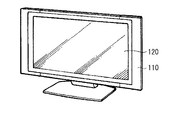
- FIG. 9 shows the appearance of the television device.
- This television device has a main body 110 and a display unit 120, and the display unit 120 is constituted by the display device described above.
- the display device includes electronic devices in various fields such as a digital camera, a notebook personal computer, a portable terminal device such as a mobile phone, a portable game machine, or a video camera in addition to such a television device. It is possible to apply to. In other words, the display device of the above embodiment and the like can be applied to electronic devices in all fields that display video.
- the present technology is applied to a television apparatus, but the present invention is not limited to this and can be applied to various apparatuses that display images. Specifically, for example, the present invention may be applied to a large display installed in a soccer field or a baseball field.
- the display unit generates a pulse signal having a pulse width corresponding to the third luminance information based on the third luminance information, and drives the light emitting element based on the pulse signal.
- (6) further comprising a signal generator for generating a reference signal having a sawtooth waveform;
- the driving unit generates the pulse signal based on the third luminance information and the reference signal.
- a display device (9) a display device; A control unit that performs operation control on the display device, The display device Having a plurality of correction tables, selecting one of the plurality of correction tables based on the first luminance information, and performing a correction operation on the first luminance information using the selected correction table; A correction unit that generates the second luminance information,
- An electronic device comprising: a display unit that performs display based on the second luminance information.
Landscapes
- Engineering & Computer Science (AREA)
- Physics & Mathematics (AREA)
- General Physics & Mathematics (AREA)
- Computer Hardware Design (AREA)
- Theoretical Computer Science (AREA)
- Chemical & Material Sciences (AREA)
- Crystallography & Structural Chemistry (AREA)
- Nonlinear Science (AREA)
- Mathematical Physics (AREA)
- Optics & Photonics (AREA)
- Control Of Indicators Other Than Cathode Ray Tubes (AREA)
- Liquid Crystal Display Device Control (AREA)
- Control Of El Displays (AREA)
- Liquid Crystal (AREA)
Abstract
本開示の表示装置は、複数の補正テーブルを有し、第1の輝度情報に基づいて複数の補正テーブルのうちの1つを選択し、選択した補正テーブルを用いて第1の輝度情報に対して補正演算を行うことにより第2の輝度情報を生成する補正部と、第2の輝度情報に基づいて表示を行う表示部とを備える。
Description
本開示は、画像を表示する表示装置、そのような表示装置において用いられる表示方法、および、そのような表示装置を備えた電子機器に関する。
表示装置は、一般に画質が高いことが望まれている。例えば、特許文献1には、発光素子に流れる電流、およびその発光素子の発光時間の両方を変化させることにより、階調表示におけるダイナミックレンジの拡大を図る表示装置が開示されている。また、例えば、特許文献2には、液晶パネルと、フレーム内の画素値の最大値および最小値に応じた発光量で発光するバックライトとを備えた表示装置が開示されている。
このように、表示装置では、画質が高いことが望まれており、さらなる画質の向上が期待されている。
したがって、画質を高めることができる表示装置、表示方法、および電子機器を提供することが望ましい。
本開示の一実施の形態における表示装置は、補正部と、表示部とを備えている。補正部は、複数の補正テーブルを有し、第1の輝度情報に基づいて複数の補正テーブルのうちの1つを選択し、選択した補正テーブルを用いて第1の輝度情報に対して補正演算を行うことにより第2の輝度情報を生成するものである。表示部は、第2の輝度情報に基づいて表示を行うものである。
本開示の一実施の形態における表示方法は、第1の輝度情報に基づいて複数の補正テーブルのうちの1つを選択し、選択した補正テーブルを用いて第1の輝度情報に対して補正演算を行うことにより第2の輝度情報を生成し、第2の輝度情報に基づいて表示を行うものである。
本開示の一実施の形態における電子機器は、上記表示装置を備えたものであり、例えば、テレビジョン装置、電子ブック、スマートフォン、デジタルカメラ、ノート型パーソナルコンピュータ、ビデオカメラ、ヘッドマウントディスプレイなどが該当する。
本開示の一実施の形態における表示装置、表示方法、および電子機器では、第1の輝度情報に対して補正演算が行われることにより、第2の補正情報が生成され、第2の輝度情報に基づいて表示が行われる。その際、第1の輝度情報に基づいて複数の補正テーブルのうちの1つが選択され、選択された補正テーブルを用いて第2の輝度情報が生成される。
本開示の一実施の形態における表示装置、表示方法、および電子機器によれば、第1の輝度情報に基づいて複数の補正テーブルのうちの1つを選択し、選択した補正テーブルを用いて第1の輝度情報に対して補正演算を行うようにしたので、画質を高めることができる。なお、ここに記載された効果は必ずしも限定されるものではなく、本開示中に記載されたいずれの効果があってもよい。
以下、本開示の実施の形態について、図面を参照して詳細に説明する。なお、説明は以下の順序で行う。
1.第1の実施の形態
2.第2の実施の形態
3.適用例
1.第1の実施の形態
2.第2の実施の形態
3.適用例
<1.第1の実施の形態>
[構成例]
図1は、第1の実施の形態に係る表示装置(表示装置1)の一構成例を表すものである。表示装置1は、LED(Light Emitting Diode)を表示素子として用いたものである。なお、本開示の実施の形態に係る表示方法は、本実施の形態により具現化されるので、併せて説明する。
[構成例]
図1は、第1の実施の形態に係る表示装置(表示装置1)の一構成例を表すものである。表示装置1は、LED(Light Emitting Diode)を表示素子として用いたものである。なお、本開示の実施の形態に係る表示方法は、本実施の形態により具現化されるので、併せて説明する。
表示装置1は、画像処理部20と、タイミング制御部11と、表示駆動部12と、表示部13を備えている。表示装置1は、画像信号Spicに基づいて、画像を表示するものである。画像信号Spicは、輝度情報INFR,INFG,INFBを含んでいる。輝度情報INFRは赤色(R)の輝度値を示すものであり、輝度情報INFGは緑色(G)の輝度値を示すものであり、輝度情報INFBは青色(B)の輝度値を示すものである。輝度情報INFR,INFG,INFBは、それぞれ、0以上、値INFmax以下の値を有するものである。以下、輝度情報INFR,INFG,INFBのいずれかを表すものとして輝度情報INFを適宜用いる。
画像処理部20は、画像信号Spicに基づいて、画像信号Spic3および制御信号Sctrlを生成するものである。
図2は、画像処理部20の一構成例を表すものである。画像処理部20は、制御信号生成部21と、補正部22と、演算部23とを有している。
制御信号生成部21は、画像信号Spicに基づいて制御信号Sctrlを生成するものである。具体的には、制御信号生成部21は、画像信号Spicに含まれる輝度情報INFの値を、所定のしきい値INFthと比較する。そして、制御信号生成部21は、輝度情報INFの値がしきい値INFthよりも大きい場合には、値が“1”である制御信号Sctrlを生成し、輝度情報INFの値がしきい値INFth以下である場合には、値が“0”である制御信号Sctrlを生成するようになっている。ここで、しきい値INFthは、例えば、値INFmaxの20分の1(INFth=INFmax/20)に設定することができる。
補正部22は、制御信号Sctrlに基づいて、画像信号Spicに含まれる輝度情報INF(INFR,INFG,INFB)を補正することにより、輝度情報INF2(INFR2,INFG2,INFB2)を生成するものである。補正部22は、補正テーブルT1,T2を有している。補正テーブルT1,T2は、表示部13における発光素子40(後述)の特性ばらつきを補正するとともに、駆動電流による発光素子40の色度変化を補正するためのものである。補正テーブルT1,T2のそれぞれは、表示部13における発光素子40の数に対応する数の補正データDを含んでいる。補正テーブルT1は、輝度情報INFの値がしきい値INFthよりも大きい場合に用いるものであり、補正テーブルT2は、輝度情報INFの値がしきい値INFth以下である場合に用いるものである。
この構成により、補正部22は、まず、制御信号Sctrlに基づいて、補正テーブルT1,T2のうちの使用する補正テーブルを選択する。具体的には、制御信号Sctrlの値が“1”である場合には、補正テーブルT1を選択し、制御信号Sctrlの値が“0”である場合には、補正テーブルT2を選択する。そして、補正部22は、選択した補正テーブルに含まれる補正データDに基づいて、輝度情報INFを補正することにより、輝度情報INF2を生成する。そして、補正部22は、これらの輝度情報INF2を、画像信号Spic2として出力するようになっている。
演算部23は、制御信号Sctrlに基づいて、画像信号Spic2に含まれる輝度情報INF2(INFR2,INFG2,INFB2)に対して演算を行うことにより、輝度情報INF3(INFR3,INFG3,INFB3)を生成するものである。具体的には、演算部23は、制御信号Sctrlの値が“1”である場合には、輝度情報INF2の値に対してゲインG1を乗算することにより輝度情報INF3を生成する。ゲインG1は、この例では“1”である。また、演算部23は、制御信号Sctrlの値が“0”である場合には、輝度情報INF2の値に対してゲインG2を乗算することにより輝度情報INF3を生成する。ゲインG2は、この例では“20”である。そして、演算部23は、輝度情報INF3を、画像信号Spic3として出力するようになっている。
図3は、演算部23の一動作例を表すものである。この例では、補正部22は、説明の便宜上、輝度情報INFに対して補正を行わず、輝度情報INFを輝度情報INF2として出力している。輝度情報INFの値がしきい値INFthよりも大きい場合には、演算部23が出力する輝度情報INF3の値は、輝度情報INF2の値と同じである。また、輝度情報INFの値がしきい値INFth以下である場合には、輝度情報INF3の値は、この例では、輝度情報INF2の値の20倍になる。このように、演算部23は、輝度情報INFの値が低い場合に、高いゲインG2を用いることにより、輝度情報INF3の値を高くする。これにより、表示装置1では、後述するように、輝度情報INFの値が低い場合において、画質が低下するおそれを低減するようになっている。
タイミング制御部11(図1)は、画像信号Spicに基づいて、表示駆動部12および表示部13がお互いに同期して動作するように制御するものである。具体的には、タイミング制御部11は、表示駆動部12に対して制御信号を供給するとともに、表示部13に対して参照信号Srefを供給するようになっている。
図4は、参照信号Srefの波形の一例を表すものである。参照信号Srefは、いわゆるのこぎり波形を有するものである。タイミング制御部11は、このような波形を有する参照信号Srefを生成し、表示部13に対して供給するようになっている。
表示駆動部12は、画像信号Spic3、およびタイミング制御部11から供給された制御信号に基づいて、画素信号Sigを生成し、その画素信号Sigを表示部13に供給するものである。
表示部13は、画素信号Sig、制御信号Sctrl、および参照信号Srefに基づいて画像を表示するものである。表示部13は、マトリックス状に配置された複数の画素Pixを有している。
図5は、画素Pixの一構成例を表すものである。画素Pixは、駆動部30と、3つの発光素子40(40R,40G,40B)とを有している。
駆動部30は、画素信号Sig、制御信号Sctrl、および参照信号Srefに基づいて、発光素子40R,40G,40Bに、駆動電流をそれぞれ供給するものである。駆動部30は、制御部31と、コンパレータ321~323と、スイッチ制御部331~333と、電流源341~346と、スイッチ351~356とを有している。
制御部31は、画素信号Sigおよび制御信号Sctrlに基づいて、画素電圧VpixR,VpixG,VpixGおよびスイッチ制御信号SELR,SELG,SELBを生成するものである。具体的には、制御部31は、画素信号Sigに含まれる、この画素Pixの輝度情報INFR3,INFG3,INFB3に基づいて、D/A(Digital/Analog)変換を行うことにより、画素電圧VpixR,VpixG,VpixBをそれぞれ生成する。また、制御部31は、制御信号Sctrlに基づいて、スイッチ制御信号SELR,SELG,SELBを生成する。具体的には、制御部31は、この画素Pixの輝度情報INFR3に対応する制御信号Sctrlをスイッチ制御信号SELRとして出力し、この画素Pixの輝度情報INFG3に対応する制御信号Sctrlをスイッチ制御信号SELGとして出力し、この画素Pixの輝度情報INFB3に対応する制御信号Sctrlをスイッチ制御信号SELBとして出力するようになっている。
コンパレータ321は、画素電圧VpixRと参照信号Srefとを比較することによりパルス信号SRを生成するものである。コンパレータ322は、画素電圧VpixGと参照信号Srefとを比較することによりパルス信号SGを生成するものである。コンパレータ323は、画素電圧VpixBと参照信号Srefとを比較することによりパルス信号SBを生成するものである。
図6は、コンパレータ321の一動作例を表すものである。なお、コンパレータ322,323についても同様である。コンパレータ321は、画素電圧VpixRと参照信号Srefとを比較することによりパルス信号SRを生成する。例えば、画素電圧VpixRが中程度(画素電圧VpixR1)である場合には、パルス信号SR(パルス信号SR1)のデューティ比は50%程度になる。また、例えば、画素電圧VpixRが低い場合(画素電圧VpixR2)である場合には、パルス信号SR(パルス信号SR2)のデューティ比は小さくなる。このように、コンパレータ321は、画素電圧VpixRに応じたパルス幅を有するパルス信号SRを生成するようになっている。
スイッチ制御部331(図5)は、スイッチ制御信号SELRおよびパルス信号SRに基づいて、スイッチ351,352を制御するものである。具体的には、スイッチ制御部331は、スイッチ制御信号SELRが“1”である場合には、パルス信号SRに基づいてスイッチ351をオンオフ制御するとともに、スイッチ352をオフ状態に維持する。また、スイッチ制御部331は、スイッチ制御信号SELRが“0”である場合には、パルス信号SRに基づいてスイッチ352をオンオフ制御するとともに、スイッチ351をオフ状態に維持するようになっている。
同様に、スイッチ制御部332は、スイッチ制御信号SELGおよびパルス信号SGに基づいて、スイッチ353,354を制御するものである。具体的には、スイッチ制御部332は、スイッチ制御信号SELGが“1”である場合には、パルス信号SGに基づいてスイッチ353をオンオフ制御するとともに、スイッチ354をオフ状態に維持する。また、スイッチ制御部332は、スイッチ制御信号SELGが“0”である場合には、パルス信号SGに基づいてスイッチ354をオンオフ制御するとともに、スイッチ353をオフ状態に維持するようになっている。
同様に、スイッチ制御部333は、スイッチ制御信号SELBおよびパルス信号SBに基づいて、スイッチ355,356を制御するものである。具体的には、スイッチ制御部333は、スイッチ制御信号SELBが“1”である場合には、パルス信号SBに基づいてスイッチ355をオンオフ制御するとともに、スイッチ356をオフ状態に維持する。また、スイッチ制御部333は、スイッチ制御信号SELBが“0”である場合には、パルス信号SBに基づいてスイッチ356をオンオフ制御するとともに、スイッチ355をオフ状態に維持するようになっている。
電流源341,343,345は、一端から他端へ、所定の駆動電流I1を流すものである。電流源342,344,346は、一端から他端へ、所定の駆動電流I2を流すものである。駆動電流I1の値は、例えば100[μA]であり、駆動電流I2の値は、例えば5[μA]である。すなわち、この例では、駆動電流I2の電流値は、駆動電流I1の“1/20”である。この駆動電流I1,I2の比I2/I1(=1/20)は、上述した演算部23におけるゲインG1,G2の比G1/G2(=1/20)と対応するものである。
電流源341の一端には電源電圧VDDが印加され、他端はスイッチ351の一端に接続されている。電流源342の一端には電源電圧VDDが印加され、他端はスイッチ352の一端に接続されている。電流源343の一端には電源電圧VDDが印加され、他端はスイッチ353の一端に接続されている。電流源344の一端には電源電圧VDDが印加され、他端はスイッチ354の一端に接続されている。電流源345の一端には電源電圧VDDが印加され、他端はスイッチ355の一端に接続されている。電流源346の一端には電源電圧VDDが印加され、他端はスイッチ356の一端に接続されている。
スイッチ351は、スイッチ制御部331から供給される制御信号に基づいて一端と他端との間をオンオフするものであり、一端は電流源341の他端に接続され、他端はスイッチ352の他端に接続されるとともに、発光素子40Rのアノードに接続されている。スイッチ352は、スイッチ制御部331から供給される制御信号に基づいて一端と他端との間をオンオフするものであり、一端は電流源342の他端に接続され、他端はスイッチ351の他端に接続されるとともに、発光素子40Rのアノードに接続されている。
スイッチ353は、スイッチ制御部332から供給される制御信号に基づいて一端と他端との間をオンオフするものであり、一端は電流源343の他端に接続され、他端はスイッチ354の他端に接続されるとともに、発光素子40Gのアノードに接続されている。スイッチ354は、スイッチ制御部332から供給される制御信号に基づいて一端と他端との間をオンオフするものであり、一端は電流源344の他端に接続され、他端はスイッチ353の他端に接続されるとともに、発光素子40Gのアノードに接続されている。
スイッチ355は、スイッチ制御部333から供給される制御信号に基づいて一端と他端との間をオンオフするものであり、一端は電流源345の他端に接続され、他端はスイッチ356の他端に接続されるとともに、発光素子40Bのアノードに接続されている。スイッチ356は、スイッチ制御部333から供給される制御信号に基づいて一端と他端との間をオンオフするものであり、一端は電流源346の他端に接続され、他端はスイッチ355の他端に接続されるとともに、発光素子40Bのアノードに接続されている。
発光素子40R,40G,40Bは、例えばLEDを用いて構成されるものであり、供給された駆動電流に基づいて発光するものである。発光素子40Rは、赤色(R)の光を射出するものであり、アノードはスイッチ351の他端およびスイッチ352の他端に接続され、カソードは接地されている。同様に、発光素子40Gは、緑色(G)の光を射出するものであり、アノードはスイッチ353の他端およびスイッチ354の他端に接続され、カソードは接地されている。発光素子40Bは、青色(B)の光を射出するものであり、アノードはスイッチ355の他端およびスイッチ356の他端に接続され、カソードは接地されている。
この構成により、駆動部30は、画素電圧VpixRに応じた長さの期間において、駆動電流を発光素子40Rに供給する。その際、駆動部30は、スイッチ制御信号SELRに応じて、電流源341,342のうちの一方を選択し、その選択された電流源が駆動電流を発光素子40Rに供給する。これにより、発光素子40Rは、画素電圧VpixRに応じた長さの期間において、駆動電流に応じた輝度で発光する。同様に、駆動部30は、画素電圧VpixGに応じた長さの期間において、スイッチ制御信号SELGに応じた電流値の駆動電流を、発光素子40Gに供給する。これにより、発光素子40Gは、画素電圧VpixGに応じた長さの期間において、駆動電流に応じた輝度で発光する。また、駆動部30は、画素電圧VpixBに応じた長さの期間において、スイッチ制御信号SELBに応じた電流値の駆動電流を、発光素子40Gに供給する。これにより、発光素子40Bは、画素電圧VpixBに応じた長さの期間において、駆動電流に応じた輝度で発光するようになっている。
ここで、輝度情報INFは、本開示における「第1の輝度情報」の一具体例に対応する。輝度情報INF2は、本開示における「第2の輝度情報」の一具体例に対応する。輝度情報INF3は、本開示における「第3の輝度情報」の一具体例に対応する。タイミング制御部11は、本開示における「信号生成部」の一具体例に対応する。
[動作および作用]
続いて、本実施の形態の表示装置1の動作および作用について説明する。
続いて、本実施の形態の表示装置1の動作および作用について説明する。
(全体動作概要)
まず、図1,2,5を参照して、表示装置1の全体動作概要を説明する。画像処理部20(図1)は、画像信号Spicに基づいて、画像信号Spic3および制御信号Sctrlを生成する。具体的には、制御信号生成部21(図2)が、画像信号Spicに基づいて制御信号Sctrlを生成する。補正部22は、補正テーブルT1,T2のうちの、制御信号Sctrlに応じた補正テーブルを用いて、画像信号Spicに含まれる輝度情報INF(INFR,INFG,INFB)を補正することにより、輝度情報INF2(INFR2,INFG2,INFB2)を生成する。演算部23は、輝度情報INF2の値に対して、ゲインG1,G2のうちの、制御信号Sctrlに応じたゲインを乗算することにより、輝度情報INF3(INFR3,INFG3,INFB3)を生成する。そして、演算部23は、この輝度情報INF3を、画像信号Spic3として出力する。タイミング制御部11(図1)は、表示駆動部12に対して制御信号を供給するとともに、表示部13に対して参照信号Srefを供給する。表示駆動部12は、画像信号Spic3に基づいて画素信号Sigを生成する。
まず、図1,2,5を参照して、表示装置1の全体動作概要を説明する。画像処理部20(図1)は、画像信号Spicに基づいて、画像信号Spic3および制御信号Sctrlを生成する。具体的には、制御信号生成部21(図2)が、画像信号Spicに基づいて制御信号Sctrlを生成する。補正部22は、補正テーブルT1,T2のうちの、制御信号Sctrlに応じた補正テーブルを用いて、画像信号Spicに含まれる輝度情報INF(INFR,INFG,INFB)を補正することにより、輝度情報INF2(INFR2,INFG2,INFB2)を生成する。演算部23は、輝度情報INF2の値に対して、ゲインG1,G2のうちの、制御信号Sctrlに応じたゲインを乗算することにより、輝度情報INF3(INFR3,INFG3,INFB3)を生成する。そして、演算部23は、この輝度情報INF3を、画像信号Spic3として出力する。タイミング制御部11(図1)は、表示駆動部12に対して制御信号を供給するとともに、表示部13に対して参照信号Srefを供給する。表示駆動部12は、画像信号Spic3に基づいて画素信号Sigを生成する。
表示部13は、画素信号Sig、制御信号Sctrl、および参照信号Srefに基づいて画像を表示する。画素Pixの制御部31(図5)は、画素信号Sigおよび制御信号Sctrlに基づいて、画素電圧VpixR,VpixG,VpixGおよびスイッチ制御信号SELR,SELG,SELBを生成する。コンパレータ321は、画素電圧VpixRと参照信号Srefとを比較することによりパルス信号SRを生成する。スイッチ制御部331は、スイッチ制御信号SELRおよびパルス信号SRに基づいて、スイッチ351,352を制御する。発光素子40Rは、電流源341,342から供給された駆動電流に基づいて発光する。コンパレータ322は、画素電圧VpixGと参照信号Srefとを比較することによりパルス信号SGを生成する。スイッチ制御部332は、スイッチ制御信号SELGおよびパルス信号SGに基づいて、スイッチ353,354を制御する。発光素子40Gは、電流源343,344から供給された駆動電流に基づいて発光する。コンパレータ323は、画素電圧VpixBと参照信号Srefとを比較することによりパルス信号SBを生成する。スイッチ制御部333は、スイッチ制御信号SELBおよびパルス信号SBに基づいて、スイッチ355,356を制御する。発光素子40Bは、電流源345,346から供給された駆動電流に基づいて発光する。
(詳細動作)
表示装置1では、輝度情報INFの値に応じて、補正テーブルT1,T2、ゲインG1,G2、駆動電流I1,I2を切り替える。具体的には、表示装置1は、輝度情報INFの値がしきい値INFthよりも大きい場合には、補正テーブルT1、ゲインG1、および駆動電流I1を用いる。ここで、ゲインG1は、例えば“1”であり、駆動電流I1は、例えば100[μA]である。また、表示装置1は、輝度情報INFの値がしきい値INFth以下である場合には、補正テーブルT2,ゲインG2、および駆動電流I2を用いる。ここで、ゲインG2は、例えば“20”であり、駆動電流I2は、例えば5[μA]である。すなわち、表示装置1は、輝度情報INFの値がしきい値INFthよりも大きい場合には、ゲインを小さくするとともに駆動電流を大きくし、輝度情報INFの値がしきい値INFth以下である場合には、ゲインを大きくするとともに駆動電流を小さくする。これにより、表示装置1では、以下に説明するように、輝度情報INFの値が低い場合において、画質が低下するおそれを低減することができる。
表示装置1では、輝度情報INFの値に応じて、補正テーブルT1,T2、ゲインG1,G2、駆動電流I1,I2を切り替える。具体的には、表示装置1は、輝度情報INFの値がしきい値INFthよりも大きい場合には、補正テーブルT1、ゲインG1、および駆動電流I1を用いる。ここで、ゲインG1は、例えば“1”であり、駆動電流I1は、例えば100[μA]である。また、表示装置1は、輝度情報INFの値がしきい値INFth以下である場合には、補正テーブルT2,ゲインG2、および駆動電流I2を用いる。ここで、ゲインG2は、例えば“20”であり、駆動電流I2は、例えば5[μA]である。すなわち、表示装置1は、輝度情報INFの値がしきい値INFthよりも大きい場合には、ゲインを小さくするとともに駆動電流を大きくし、輝度情報INFの値がしきい値INFth以下である場合には、ゲインを大きくするとともに駆動電流を小さくする。これにより、表示装置1では、以下に説明するように、輝度情報INFの値が低い場合において、画質が低下するおそれを低減することができる。
図7は、輝度情報INFRの値が低い場合におけるパルス信号SRの波形を表すものである。輝度情報INFRの値が低い場合には、画素電圧VpixRもまた低くなる。図7に示したように、画素電圧VpixRが低い場合には、パルス信号SRのデューティ比が小さくなる。参照信号Srefは、いわゆるのこぎり波形を有するものである。よって、寄生抵抗や寄生容量の影響を受け、例えば、図7に示した部分Wの波形がなまってしまうおそれがある。このように波形の一部がなまってしまった場合には、パルス信号SRのデューティ比は、画素電圧VpixRに対応する理想的なデューティ比からずれてしまい、その結果、画質が低下するおそれがある。
表示装置1では、輝度情報INFの値がしきい値INFth以下である場合には、輝度情報INF2に、大きいゲインG2を乗算することにより、輝度情報INF3を生成する。これにより、表示装置1では、例えば、画素電圧VpixRが高くなるため、輝度情報INFRの値が低い場合でも、図7に示した部分Wを使用する機会が少なくなる。その結果、表示装置1では、パルス信号SRのデューティ比が、画素電圧VpixRに対応する理想的なデューティ比からずれるおそれを低減することができ、画質を高めることができる。
また、表示装置1では、輝度情報INFの値に応じて、補正テーブルT1,T2を切り替えるようにしたので、画質を高めることができる。すなわち、まず、表示装置1では、ゲインG1,G2の切り替えに応じて、駆動電流I1,I2を切り替える。発光素子は、一般に、駆動電流が変化すると、輝度が変化するだけでなく、色度が変化するおそれがある。表示装置1では、輝度情報INFの値に応じて、駆動電流I1,I2を切り替えるとともに、補正テーブルT1,T2を切り替えるようにしたので、駆動電流に応じて色度の変化を補正することができるため、画質を高めることができる。
[効果]
以上のように本実施の形態では、輝度情報の値に応じて、ゲインおよび駆動電流を切り替えるようにしたので、画質を高めることができる。
以上のように本実施の形態では、輝度情報の値に応じて、ゲインおよび駆動電流を切り替えるようにしたので、画質を高めることができる。
本実施の形態では、輝度情報の値に応じて、補正テーブルを切り替えるようにしたので、色度を補正することができるため、画質を高めることができる。
[変形例1-1]
上記実施の形態では、LEDを用いて発光素子40を構成したが、これに限定されるものではなく、例えば、レーザダイオードや、EL(Electro Luminescence)素子などを用いて構成してもよい。
上記実施の形態では、LEDを用いて発光素子40を構成したが、これに限定されるものではなく、例えば、レーザダイオードや、EL(Electro Luminescence)素子などを用いて構成してもよい。
[変形例1-2]
上記実施の形態では、2つの補正テーブルT1,T2を設けたが、これに限定されるものではなく、これに代えて、例えば3つ以上の補正テーブルを設けてもよい。具体的には、例えば、輝度情報INFの値に応じて、3つの補正テーブルのうちの1つを選択し、3つのゲインのうちの1つを選択し、3つの駆動電流のうちの1つを選択するようにしてもよい。
上記実施の形態では、2つの補正テーブルT1,T2を設けたが、これに限定されるものではなく、これに代えて、例えば3つ以上の補正テーブルを設けてもよい。具体的には、例えば、輝度情報INFの値に応じて、3つの補正テーブルのうちの1つを選択し、3つのゲインのうちの1つを選択し、3つの駆動電流のうちの1つを選択するようにしてもよい。
<2.第2の実施の形態>
次に、第2の実施の形態に係る表示装置2について説明する。本実施の形態は、本技術を液晶表示装置に適用したものである。なお、上記第1の実施の形態に係る表示装置と実質的に同一の構成部分には同一の符号を付し、適宜説明を省略する。
次に、第2の実施の形態に係る表示装置2について説明する。本実施の形態は、本技術を液晶表示装置に適用したものである。なお、上記第1の実施の形態に係る表示装置と実質的に同一の構成部分には同一の符号を付し、適宜説明を省略する。
図8は、表示装置2の一構成例を表すものである。表示装置2は、画像処理部50と、タイミング制御部41と、表示駆動部42と、走査部43と、液晶表示部44と、バックライト45とを有している。
画像処理部50は、図2に示したように、制御信号生成部51を有している。制御信号生成部51は、画像信号Spicに基づいて、1フレーム分の輝度情報INFの値の平均値AVGを求め、その平均値AVGと所定のしきい値INFthと比較することにより、制御信号Sctrlを生成するものである。具体的には、制御信号生成部51は、平均値AVGがしきい値INFthよりも大きい場合には、値が“1”である制御信号Sctrlを生成し、平均値AVGがしきい値INFth以下である場合には、値が“0”である制御信号Sctrlを生成するようになっている。
タイミング制御部41は、画像信号Spicに基づいて、表示駆動部42および走査部43に対してそれぞれ制御信号を供給することにより、表示駆動部42および走査部43がお互いに同期して動作するように制御するものである。
表示駆動部42は、画像信号Spic3、およびタイミング制御部41から供給された制御信号に基づいて、輝度情報INF3に対してD/A変換を行うことにより、画素電圧Vpixを生成するものである。そして、表示駆動部42を、その画素電圧Vpixを、画素信号Sig2として出力するようになっている。
走査部32は、タイミング制御部41から供給された制御信号に基づいて、液晶表示部44の画素Pix2(後述)をライン単位で選択するための走査信号Scanを生成するものである。
液晶表示部44は、画素信号Sig2および走査信号Scanに基づいて画像を表示するものである。液晶表示部44は、マトリックス状に配置された複数の画素Pix2を有している。画素Pix2は、赤色の光を透過させるサブ画素と、緑色の光を透過させるサブ画素と、青色の光を透過させるサブ画素とを有している。各サブ画素は、画素電圧Vpixに基づいて、バックライト45から射出された光の透過率を変化させるものである。
バックライト45は、液晶表示部44に対して白色光を射出するものである。バックライト45は、例えば、赤色の光を射出するLEDと、緑色の光を射出するLEDと、青色の光を射出するLEDとを含み、これらの光が混ざり合った白色光を射出する。このバックライト45は、制御信号Sctrlに基づいて、発光輝度を変更可能に構成されている。具体的には、制御信号Sctrlに基づいて、これらのLEDに駆動電流I1または駆動電流I2を流すように構成されている。
表示装置2では、上記実施の形態に係る表示装置1と同様に、輝度情報INFの値に応じて、補正テーブルT1,T2、ゲインG1,G2、駆動電流I1,I2を切り替える。すなわち、表示装置2では、輝度情報INFの値がしきい値INFthよりも大きい場合には、ゲインを小さくするとともに駆動電流を大きくし、輝度情報INFの値がしきい値INFth以下である場合には、ゲインを大きくするとともに駆動電流を小さくする。その際、表示装置2は、駆動電流I1,I2に応じて補正テーブルT1,T2を切り替えるようにしたので、画質を高めることができる。すなわち、バックライト45の各LEDは、駆動電流が変化すると、輝度が変化するだけでなく、色度が変化するおそれがある。表示装置2では、輝度情報INFの値に応じて、駆動電流I1,I2を切り替えるとともに、補正テーブルT1,T2を切り替えるようにしたので、駆動電流に応じて色度の変化を補正することができるため、画質を高めることができる。
本実施の形態では、輝度情報の値に応じて、補正テーブルを切り替えるようにしたので、色度を補正することができるため、画質を高めることができる。
[変形例2-1]
上記実施の形態では、制御信号生成部51は、1フレーム分の輝度情報INFの値の平均値AVGを求めることにより制御信号Sctrlを生成し、バックライト45は、この制御信号Sctrlに基づいて発光輝度を変更するようにしたが、これに限定されるものではない。例えば、バックライト45の発光面を複数の発光領域に分け、制御信号生成部51は、それらの発光領域に対応する領域ごとに輝度情報INFの値の平均値AVGを求めてもよい。
上記実施の形態では、制御信号生成部51は、1フレーム分の輝度情報INFの値の平均値AVGを求めることにより制御信号Sctrlを生成し、バックライト45は、この制御信号Sctrlに基づいて発光輝度を変更するようにしたが、これに限定されるものではない。例えば、バックライト45の発光面を複数の発光領域に分け、制御信号生成部51は、それらの発光領域に対応する領域ごとに輝度情報INFの値の平均値AVGを求めてもよい。
<3.適用例>
次に、上記実施の形態および変形例で説明した表示装置の適用例について説明する。
次に、上記実施の形態および変形例で説明した表示装置の適用例について説明する。
図9は、テレビジョン装置の外観を表すものである。このテレビジョン装置は、本体部110および表示部120を有しており、表示部120が、上記の表示装置により構成されている。
上記実施の形態等の表示装置は、このようなテレビジョン装置の他、デジタルカメラ、ノート型パーソナルコンピュータ、携帯電話等の携帯端末装置、携帯型ゲーム機、あるいはビデオカメラなどのあらゆる分野の電子機器に適用することが可能である。言い換えると、上記実施の形態等の表示装置は、映像を表示するあらゆる分野の電子機器に適用することが可能である。
以上、いくつかの実施の形態および変形例、ならびに電子機器への適用例を挙げて本技術を説明したが、本技術はこれらの実施の形態等には限定されず、種々の変形が可能である。
上記の実施の形態等では、本技術をテレビジョン装置に適用したが、これに限定するものではなく、画像を表示する様々な装置に適用することができる。具体的には、例えば、サッカー場や野球場などに設置される大型のディスプレイに適用してもよい。
なお、本明細書に記載された効果はあくまで例示であって限定されるものでは無く、また他の効果があってもよい。
なお、本技術は以下のような構成とすることができる。
(1)複数の補正テーブルを有し、第1の輝度情報に基づいて前記複数の補正テーブルのうちの1つを選択し、選択した補正テーブルを用いて前記第1の輝度情報に対して補正演算を行うことにより第2の輝度情報を生成する補正部と、
前記第2の輝度情報に基づいて表示を行う表示部と
を備えた表示装置。
前記第2の輝度情報に基づいて表示を行う表示部と
を備えた表示装置。
(2)前記第1の輝度情報に基づいて制御信号を生成する制御信号生成部と、
前記第2の輝度情報に対して、前記制御信号に応じた演算を行うことにより第3の輝度情報を生成する演算部と
をさらに備え、
前記補正部は、前記制御信号に基づいて、前記複数の補正テーブルのうちの1つを選択し、
前記表示部は、前記第3の輝度情報に基づいて表示を行う
前記(1)に記載の表示装置。
前記第2の輝度情報に対して、前記制御信号に応じた演算を行うことにより第3の輝度情報を生成する演算部と
をさらに備え、
前記補正部は、前記制御信号に基づいて、前記複数の補正テーブルのうちの1つを選択し、
前記表示部は、前記第3の輝度情報に基づいて表示を行う
前記(1)に記載の表示装置。
(3)前記演算部は、前記第2の輝度情報の値に対して、前記制御信号に応じたゲインを乗算することにより前記第3の輝度情報を生成する
前記(2)に記載の表示装置。
前記(2)に記載の表示装置。
(4)前記表示部は、前記制御信号に応じた輝度で発光する発光素子を有する
前記(2)または(3)に記載の表示装置。
前記(2)または(3)に記載の表示装置。
(5)前記表示部は、前記第3の輝度情報に基づいて、前記第3の輝度情報に応じたパルス幅を有するパルス信号を生成し、そのパルス信号に基づいて前記発光素子を駆動する駆動部をさらに有する
前記(4)に記載の表示装置。
前記(4)に記載の表示装置。
(6)のこぎり波形を有する参照信号を生成する信号生成部をさらに備え、
前記駆動部は、前記第3の輝度情報および前記参照信号に基づいて、前記パルス信号を生成する
前記(5)に記載の表示装置。
前記駆動部は、前記第3の輝度情報および前記参照信号に基づいて、前記パルス信号を生成する
前記(5)に記載の表示装置。
(7)前記制御信号に応じた輝度で発光するバックライトをさらに備え、
前記表示部は、液晶表示部である
前記(2)または(3)に記載の表示装置。
前記表示部は、液晶表示部である
前記(2)または(3)に記載の表示装置。
(8)第1の輝度情報に基づいて複数の補正テーブルのうちの1つを選択し、
選択した補正テーブルを用いて前記第1の輝度情報に対して補正演算を行うことにより第2の輝度情報を生成し、
前記第2の輝度情報に基づいて表示を行う
表示方法。
選択した補正テーブルを用いて前記第1の輝度情報に対して補正演算を行うことにより第2の輝度情報を生成し、
前記第2の輝度情報に基づいて表示を行う
表示方法。
(9)表示装置と、
前記表示装置に対して動作制御を行う制御部と
を備え、
前記表示装置は、
複数の補正テーブルを有し、第1の輝度情報に基づいて前記複数の補正テーブルのうちの1つを選択し、選択した補正テーブルを用いて前記第1の輝度情報に対して補正演算を行うことにより第2の輝度情報を生成する補正部と、
前記第2の輝度情報に基づいて表示を行う表示部と
を有する電子機器。
前記表示装置に対して動作制御を行う制御部と
を備え、
前記表示装置は、
複数の補正テーブルを有し、第1の輝度情報に基づいて前記複数の補正テーブルのうちの1つを選択し、選択した補正テーブルを用いて前記第1の輝度情報に対して補正演算を行うことにより第2の輝度情報を生成する補正部と、
前記第2の輝度情報に基づいて表示を行う表示部と
を有する電子機器。
本出願は、日本国特許庁において2015年5月8日に出願された日本特許出願番号2015-95495号を基礎として優先権を主張するものであり、この出願のすべての内容を参照によって本出願に援用する。
当業者であれば、設計上の要件や他の要因に応じて、種々の修正、コンビネーション、サブコンビネーション、および変更を想到し得るが、それらは添付の請求の範囲やその均等物の範囲に含まれるものであることが理解される。
Claims (9)
- 複数の補正テーブルを有し、第1の輝度情報に基づいて前記複数の補正テーブルのうちの1つを選択し、選択した補正テーブルを用いて前記第1の輝度情報に対して補正演算を行うことにより第2の輝度情報を生成する補正部と、
前記第2の輝度情報に基づいて表示を行う表示部と
を備えた表示装置。 - 前記第1の輝度情報に基づいて制御信号を生成する制御信号生成部と、
前記第2の輝度情報に対して、前記制御信号に応じた演算を行うことにより第3の輝度情報を生成する演算部と
をさらに備え、
前記補正部は、前記制御信号に基づいて、前記複数の補正テーブルのうちの1つを選択し、
前記表示部は、前記第3の輝度情報に基づいて表示を行う
請求項1に記載の表示装置。 - 前記演算部は、前記第2の輝度情報の値に対して、前記制御信号に応じたゲインを乗算することにより前記第3の輝度情報を生成する
請求項2に記載の表示装置。 - 前記表示部は、前記制御信号に応じた輝度で発光する発光素子を有する
請求項2に記載の表示装置。 - 前記表示部は、前記第3の輝度情報に基づいて、前記第3の輝度情報に応じたパルス幅を有するパルス信号を生成し、そのパルス信号に基づいて前記発光素子を駆動する駆動部をさらに有する
請求項4に記載の表示装置。 - のこぎり波形を有する参照信号を生成する信号生成部をさらに備え、
前記駆動部は、前記第3の輝度情報および前記参照信号に基づいて、前記パルス信号を生成する
請求項5に記載の表示装置。 - 前記制御信号に応じた輝度で発光するバックライトをさらに備え、
前記表示部は、液晶表示部である
請求項2に記載の表示装置。 - 第1の輝度情報に基づいて複数の補正テーブルのうちの1つを選択し、
選択した補正テーブルを用いて前記第1の輝度情報に対して補正演算を行うことにより第2の輝度情報を生成し、
前記第2の輝度情報に基づいて表示を行う
表示方法。 - 表示装置と、
前記表示装置に対して動作制御を行う制御部と
を備え、
前記表示装置は、
複数の補正テーブルを有し、第1の輝度情報に基づいて前記複数の補正テーブルのうちの1つを選択し、選択した補正テーブルを用いて前記第1の輝度情報に対して補正演算を行うことにより第2の輝度情報を生成する補正部と、
前記第2の輝度情報に基づいて表示を行う表示部と
を有する電子機器。
Applications Claiming Priority (2)
| Application Number | Priority Date | Filing Date | Title |
|---|---|---|---|
| JP2015095495A JP2016212239A (ja) | 2015-05-08 | 2015-05-08 | 表示装置、表示方法、および電子機器 |
| JP2015-095495 | 2015-05-08 |
Publications (1)
| Publication Number | Publication Date |
|---|---|
| WO2016181757A1 true WO2016181757A1 (ja) | 2016-11-17 |
Family
ID=57247917
Family Applications (1)
| Application Number | Title | Priority Date | Filing Date |
|---|---|---|---|
| PCT/JP2016/062087 Ceased WO2016181757A1 (ja) | 2015-05-08 | 2016-04-15 | 表示装置、表示方法、および電子機器 |
Country Status (2)
| Country | Link |
|---|---|
| JP (1) | JP2016212239A (ja) |
| WO (1) | WO2016181757A1 (ja) |
Families Citing this family (6)
| Publication number | Priority date | Publication date | Assignee | Title |
|---|---|---|---|---|
| JP2018106049A (ja) * | 2016-12-27 | 2018-07-05 | ソニー株式会社 | 光源装置、発光装置、および表示装置 |
| FR3076396B1 (fr) * | 2017-12-28 | 2021-12-03 | Aledia | Ecran d'affichage a diodes electroluminescentes |
| WO2021020042A1 (ja) * | 2019-07-31 | 2021-02-04 | 京セラ株式会社 | 表示装置 |
| WO2021038794A1 (ja) * | 2019-08-29 | 2021-03-04 | 三菱電機株式会社 | Led表示装置 |
| WO2021100145A1 (ja) * | 2019-11-20 | 2021-05-27 | 三菱電機株式会社 | Led表示装置、及びled表示装置の輝度補正方法 |
| CN116457863A (zh) * | 2020-11-10 | 2023-07-18 | 索尼集团公司 | 发光装置、发光装置的驱动方法以及电子设备 |
Citations (3)
| Publication number | Priority date | Publication date | Assignee | Title |
|---|---|---|---|---|
| JP2008503775A (ja) * | 2004-06-16 | 2008-02-07 | イーストマン コダック カンパニー | Oledディスプレイの均一性と明るさの補正 |
| JP2010044250A (ja) * | 2008-08-13 | 2010-02-25 | Hitachi Displays Ltd | 画像表示装置 |
| JP2014068131A (ja) * | 2012-09-25 | 2014-04-17 | Sharp Corp | 画像処理装置 |
-
2015
- 2015-05-08 JP JP2015095495A patent/JP2016212239A/ja active Pending
-
2016
- 2016-04-15 WO PCT/JP2016/062087 patent/WO2016181757A1/ja not_active Ceased
Patent Citations (3)
| Publication number | Priority date | Publication date | Assignee | Title |
|---|---|---|---|---|
| JP2008503775A (ja) * | 2004-06-16 | 2008-02-07 | イーストマン コダック カンパニー | Oledディスプレイの均一性と明るさの補正 |
| JP2010044250A (ja) * | 2008-08-13 | 2010-02-25 | Hitachi Displays Ltd | 画像表示装置 |
| JP2014068131A (ja) * | 2012-09-25 | 2014-04-17 | Sharp Corp | 画像処理装置 |
Also Published As
| Publication number | Publication date |
|---|---|
| JP2016212239A (ja) | 2016-12-15 |
Similar Documents
| Publication | Publication Date | Title |
|---|---|---|
| KR102723557B1 (ko) | 표시 장치 및 그 구동 방법 | |
| US9984614B2 (en) | Organic light emitting display device and method of driving the same | |
| JP5485396B2 (ja) | 有機el表示装置 | |
| CN113692612B (zh) | 显示装置、显示装置的驱动方法以及电子设备 | |
| US20230162666A1 (en) | Pixel circuit | |
| US20150138258A1 (en) | Organic light-emitting diode (oled) display | |
| US20150187277A1 (en) | Display unit, driving method and electronic apparatus | |
| JP2016212239A (ja) | 表示装置、表示方法、および電子機器 | |
| WO2018123280A1 (ja) | 光源装置、発光装置、および表示装置 | |
| US10971050B2 (en) | Method for driving a display panel to display image, display apparatus thereof, and driver enabled to perform the method | |
| JP2007529778A (ja) | 低輝度での画素間の非均一性改善を伴うアクティブマトリクスディスプレイ | |
| CN103886851A (zh) | 显示单元、图像处理装置、显示方法和电子设备 | |
| KR102718330B1 (ko) | 표시 장치 및 표시 장치의 구동 방법 | |
| WO2012063285A1 (ja) | 有機el表示パネル及びその駆動方法 | |
| JP2019095770A (ja) | 有機発光表示装置及びその駆動方法 | |
| JP2016099468A (ja) | 表示装置および表示方法 | |
| US20150070377A1 (en) | Image signal processing circuit, image signal processing method and display apparatus | |
| JP2005326830A (ja) | 表示装置 | |
| US10152909B2 (en) | Display apparatus | |
| CN103021311A (zh) | 显示装置、显示方法和电子系统 | |
| JP2005300929A (ja) | 表示装置 | |
| JP4569107B2 (ja) | 表示装置及び表示装置の駆動方法 | |
| CN112992067B (zh) | 实现局部高亮度的显示设备 | |
| KR101940760B1 (ko) | 유기발광 다이오드 표시장치 및 그 구동방법 | |
| WO2013018822A1 (ja) | 画像表示装置および画像表示方法 |
Legal Events
| Date | Code | Title | Description |
|---|---|---|---|
| 121 | Ep: the epo has been informed by wipo that ep was designated in this application |
Ref document number: 16792482 Country of ref document: EP Kind code of ref document: A1 |
|
| NENP | Non-entry into the national phase |
Ref country code: DE |
|
| 122 | Ep: pct application non-entry in european phase |
Ref document number: 16792482 Country of ref document: EP Kind code of ref document: A1 |