WO2016178332A1 - Programmable logic device, method for verifying error of programmable logic device, and method for forming circuit of programmable logic device - Google Patents
Programmable logic device, method for verifying error of programmable logic device, and method for forming circuit of programmable logic device Download PDFInfo
- Publication number
- WO2016178332A1 WO2016178332A1 PCT/JP2016/055389 JP2016055389W WO2016178332A1 WO 2016178332 A1 WO2016178332 A1 WO 2016178332A1 JP 2016055389 W JP2016055389 W JP 2016055389W WO 2016178332 A1 WO2016178332 A1 WO 2016178332A1
- Authority
- WO
- WIPO (PCT)
- Prior art keywords
- circuit
- arithmetic
- programmable logic
- verification
- logic device
- Prior art date
Links
Images


Classifications
-
- H—ELECTRICITY
- H03—ELECTRONIC CIRCUITRY
- H03K—PULSE TECHNIQUE
- H03K19/00—Logic circuits, i.e. having at least two inputs acting on one output; Inverting circuits
- H03K19/02—Logic circuits, i.e. having at least two inputs acting on one output; Inverting circuits using specified components
- H03K19/173—Logic circuits, i.e. having at least two inputs acting on one output; Inverting circuits using specified components using elementary logic circuits as components
- H03K19/177—Logic circuits, i.e. having at least two inputs acting on one output; Inverting circuits using specified components using elementary logic circuits as components arranged in matrix form
- H03K19/17724—Structural details of logic blocks
-
- G—PHYSICS
- G06—COMPUTING; CALCULATING OR COUNTING
- G06F—ELECTRIC DIGITAL DATA PROCESSING
- G06F7/00—Methods or arrangements for processing data by operating upon the order or content of the data handled
- G06F7/02—Comparing digital values
-
- G—PHYSICS
- G06—COMPUTING; CALCULATING OR COUNTING
- G06F—ELECTRIC DIGITAL DATA PROCESSING
- G06F7/00—Methods or arrangements for processing data by operating upon the order or content of the data handled
- G06F7/38—Methods or arrangements for performing computations using exclusively denominational number representation, e.g. using binary, ternary, decimal representation
- G06F7/48—Methods or arrangements for performing computations using exclusively denominational number representation, e.g. using binary, ternary, decimal representation using non-contact-making devices, e.g. tube, solid state device; using unspecified devices
- G06F7/483—Computations with numbers represented by a non-linear combination of denominational numbers, e.g. rational numbers, logarithmic number system or floating-point numbers
-
- H—ELECTRICITY
- H03—ELECTRONIC CIRCUITRY
- H03K—PULSE TECHNIQUE
- H03K19/00—Logic circuits, i.e. having at least two inputs acting on one output; Inverting circuits
- H03K19/02—Logic circuits, i.e. having at least two inputs acting on one output; Inverting circuits using specified components
- H03K19/173—Logic circuits, i.e. having at least two inputs acting on one output; Inverting circuits using specified components using elementary logic circuits as components
Definitions
- the present invention relates to a programmable logic device, a programmable logic device error verification method, and a programmable logic device circuit formation method.
- programmable logic devices especially FPGA (Field Programmable Gate Array) have come to be widely used in the field of control and communication.
- the FPGA loads the configuration information into the configuration memory in the FPGA, thereby combining arithmetic circuit by combining circuit blocks such as basic logic blocks (also called CLB (Configurable Logic Block), LE (Logic Element), etc.).
- CLB Configurable Logic Block
- LE Logic Element
- Various arithmetic circuits can be realized, ranging from those that perform simple numerical operations to those that have a function corresponding to a CPU (Central Processing Unit) (for example, see Patent Document 1).
- CPU Central Processing Unit
- each calculation that realizes a calculation function corresponds to a circuit block, and various calculation functions are realized by changing the combination of the circuit blocks. For this reason, in the FPGA, the number of circuit blocks used in the arithmetic circuit increases as the number of arithmetic functions increases. As a result, in a FPGA, when a complex arithmetic circuit having a large number of circuit blocks is formed, an AND gate in the circuit block used for the arithmetic circuit is increased as the number of circuit blocks used for the arithmetic circuit increases. The number of circuit elements such as OR gates also increases.
- circuit elements such as AND gates and OR gates may malfunction due to the influence of charged particles in the atmosphere.
- a circuit element incorporated in the arithmetic circuit malfunctions, an arithmetic result of the arithmetic circuit becomes an error. Therefore, in an FPGA, when the number of circuit elements used in an arithmetic circuit increases, the number of circuit elements increases, so the probability of being affected by charged particles in the atmosphere increases, and there is a high risk of errors. There is a problem of becoming.
- the arithmetic circuit is made redundant with a plurality of arithmetic circuits that combine the same types of circuit blocks and perform the same arithmetic processing. For this reason, when an error due to a factor common to the entire FPGA (hereinafter referred to as a common factor) such as a temperature variation of the FPGA itself, a voltage variation of the FPGA power supply, a clock variation for driving the FPGA, or the like occurs, In spite of an error occurring in the calculation result obtained from each of the calculation circuits, there is a problem that the same calculation result is obtained and the occurrence of the error cannot be detected in some cases. Therefore, the conventional error verification method cannot be said to have a sufficiently high error detection rate.
- a common factor such as a temperature variation of the FPGA itself, a voltage variation of the FPGA power supply, a clock variation for driving the FPGA, or the like.
- the present invention has been made in view of the above circumstances, and provides a programmable logic device, an error verification method for a programmable logic device, and a circuit formation method for a programmable logic device capable of improving the error detection rate as compared with the conventional technology. For the purpose.
- the present invention provides a first arithmetic circuit and a second arithmetic circuit that are different in combination and connection state of circuit blocks and perform the same operation in a programmable logic device that can change an arithmetic function by changing a combination of a plurality of circuit blocks.
- Arithmetic circuit, and provided in each of the first arithmetic circuit and the second arithmetic circuit, the verification circuit for verifying the arithmetic result includes an output unit for outputting the arithmetic result of the first arithmetic circuit and the second arithmetic circuit It is.
- the present invention also relates to an error verification method for a programmable logic device that can change an arithmetic function by changing a combination of a plurality of circuit blocks.
- a circuit formation step for forming one arithmetic circuit and a second arithmetic circuit, an arithmetic step for performing arithmetic operations in the first arithmetic circuit and the second arithmetic circuit, respectively, and the arithmetic results from the first arithmetic circuit and the second arithmetic circuit are verified. And a verification step.
- the present invention sequentially sets synthesis parameters having different conditions regarding the combination of circuit blocks in a circuit formation method for a programmable logic device capable of changing an arithmetic function by changing a combination of a plurality of circuit blocks according to configuration information.
- a synthesis parameter is set in the synthesis parameter setting step and the synthesis parameter setting step, logic synthesis is performed under the set synthesis parameter, and a plurality of arithmetic circuit description information described in the hardware description language are used.
- a set of circuit blocks The first arithmetic circuit and the second arithmetic circuit that are different from each other in the combination and connection state and perform the same arithmetic operation, and the first arithmetic circuit and the second arithmetic circuit are provided in the first arithmetic circuit and the second arithmetic circuit, respectively. Forming a circuit and an output unit for outputting a calculation result of the second calculation circuit in a programmable logic device.
- each arithmetic circuit has different operation states for common factors of temperature fluctuation, voltage fluctuation, and clock fluctuation depending on the combination of circuit blocks. Since the error occurrence state that occurs at the same time also differs, when comparing the calculation results obtained from each calculation circuit, compared to the conventional calculation results obtained from a plurality of redundant calculation circuits. Thus, errors caused by common factors can be detected, and thus the error detection rate can be improved as compared with the conventional case.
- the circuit formation method of the programmable logic device of the present invention by applying the configuration information generated from a plurality of netlists to the programmable logic device, the plurality of combinations having the same arithmetic function and different circuit blocks are provided. Can be formed in the programmable logic device.
- the operation state of each arithmetic circuit for common factors of temperature fluctuation, voltage fluctuation, and clock fluctuation differs depending on the combination of circuit blocks. Since the error occurrence state that occurs at the same time also differs, when comparing the calculation results obtained from each calculation circuit, compared to the conventional calculation results obtained from a plurality of redundant calculation circuits. Thus, errors caused by common factors can be detected, and thus the error detection rate can be improved as compared with the conventional case.
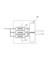
- FIG. 1 shows an FPGA (Field Programmable Gate Array) 10 used in this embodiment.
- FPGA Field Programmable Gate Array
- the FPGA 10 is a device that can change arithmetic functions such as a communication processing function, an encryption processing function, and an image processing function.
- the FPGA 10 includes a basic logic block 11, a DSP block 12, a block RAM 13, an IO block (Input / Output block) in order to realize a desired calculation function in accordance with the type of signal to be calculated and the content of the calculation process. 14, PLL block 15 and the like are provided as circuit blocks (circuit elements).
- the FPGA 10 is provided with a configuration memory 16 and wiring resources (not shown) for connecting the circuit blocks.
- the basic logic block 11 is a basic circuit block constituting the FPGA 10, and is also referred to as a CLB (Configurable Logic Block), a logic element (Logic Element), a logic cell (Logic Cell), or the like.
- the basic logic block 11 has various configurations, but in general, a plurality of basic circuits having a LUT (Lookup table) and a register (flip-flop) as basic elements (sometimes referred to as a slice or the like). It is composed of
- the DSP block 12 is not a combination of the basic logic blocks 11, but is a circuit block that is incorporated in advance as hardware (hardware macro) in order to process operations such as multiplication and product-sum operations at high speed. Sometimes called.
- the DSP block 12 is composed of a high-speed multiplier and adder as basic elements.
- the block RAM 13 is a circuit block that can be used as a general memory. The block RAM 13 is used, for example, when temporarily storing data that is being output from other circuit blocks.
- the IO block 14 is a circuit block that provides an input function and an output function of the FPGA 10.
- the PLL block 15 generates a clock necessary for the operation of the circuit block.
- the wiring resource is composed of a wiring connecting circuit blocks and a pass transistor provided on the wiring.
- Configuration information 18 is loaded (written) into the configuration memory 16.
- the configuration information 18 defines the operation of the circuit block, the connection between the circuit blocks by wiring resources, and is called configuration data, a bit stream, or the like.
- a desired arithmetic circuit is formed in the FPGA 10 according to the configuration information 18.
- the FPGA 10 is a device in which the combination of a plurality of circuit blocks is changed in accordance with the configuration information 18 and the arithmetic function can be changed thereby.
- the FPGA 10 loads the configuration information 18 having the same calculation function and forms a plurality of calculation circuits having different combinations and connection states of circuit blocks into the configuration memory 16.
- arithmetic circuits L1 to L3 and a verification circuit 21 are formed. That is, at least a first arithmetic circuit and a second arithmetic circuit are formed in the FPGA 10. Further, in the arithmetic circuits L1 to L3, output units L1a to L3a for outputting the operation results of the corresponding operation circuits are formed in the verification circuit 21 for verifying the operation results, respectively.
- the configuration information 18 may be loaded into the configuration memory 16 from an external computer, or may be automatically loaded from a nonvolatile memory in which the configuration information 18 is written in advance.
- p (p ⁇ 1) -bit input data X (x 1 to x p ) is input to the FPGA 10 in this example.
- the input data X is not limited to representing one value.
- a plurality of detection values may be combined into the input data X.
- the total number of bits of the plurality of detection values is p bits.
- the input data X may be, for example, one or more sets of numerical values generated by a computer, data received via a network, timing signals for controlling driving of various devices, and the like.
- the above input data X is input to the arithmetic circuits L1 to L3 in the FPGA 10, respectively.
- the arithmetic circuit L1 performs a predetermined operation and outputs q (q ⁇ 1) bits of operation result data V1 (v 11 to v 1q ).
- a predetermined calculation is performed, and calculation result data V2 (v 21 to v 2q ) and V3 (v 31 to v 3q ) are output. .
- the arithmetic circuits L1 to L3 have the same arithmetic function, but in order to improve the error detection rate, the combinations and connection states of the circuit blocks are different from each other. That is, the arithmetic circuits L1 to L3 have different types and numbers of circuit blocks to be used, how to use LUTs and registers in the circuit blocks, and the connection states of these circuit blocks in the arithmetic circuits L1 to L3. However, when no error occurs in the arithmetic circuits L1 to L3, the arithmetic circuits L1 to L3 are configured to output the same arithmetic result data V1 to V3 in response to the input of the same input data X. . From the viewpoint that the combination and connection state of the circuit blocks are different from each other, the arithmetic circuits L1 to L3 are in a relationship between the first arithmetic circuit and the second arithmetic circuit.
- the arithmetic circuits L1 and L3 have a circuit configuration in which at least one DSP block 12 is included in a plurality of circuit blocks to be combined.
- the arithmetic circuit L2 has a circuit configuration in which circuit blocks other than the DSP block 12 are combined (for example, a circuit configuration mainly including the basic logic block 11 including the LUT). Therefore, from the viewpoint of whether or not the circuit configuration includes the DSP block 12, the arithmetic circuits L1 and L3 correspond to the first arithmetic circuit, and the arithmetic circuit L2 corresponds to the second arithmetic circuit.
- the arithmetic circuit L1 and the arithmetic circuit L2 use, for example, a block RAM 13 as a memory for holding data being calculated (hereinafter referred to as a data holding memory), whereas the arithmetic circuit L3 has a basic logic block 11 configuration.
- a block RAM 13 as a memory for holding data being calculated
- the arithmetic circuit L3 has a basic logic block 11 configuration.
- This is a combination of circuit blocks using a so-called distributed RAM using flip-flops. In this way, the arithmetic circuits L1 to L3 use different types of circuit blocks, and the combinations of the circuit blocks are different from each other.
- the DSP block 12 When the DSP block 12 is used like the arithmetic circuits L1 and L3, the number of the basic logic blocks 11 used is greatly reduced compared to the case where the DSP block 12 is not used like the arithmetic circuit L2.
- the combination of the circuit blocks 11 forming the arithmetic circuit including the length of the wiring connecting the circuit blocks can be greatly varied. That is, the arithmetic circuits L1 and L3 and the arithmetic circuit L2 have the same logical arithmetic function, but the operation at the gate level (physical process of signal processing, behavior inside the element at the physical property level, etc.) is greatly different.
- the verification circuit 21 is formed in the FPGA 10 by combining a plurality of circuit blocks.
- the output units L1a to L3a send the operation result data V1 to V3 to the verification circuit 21.
- the verification circuit 21 verifies the operation result data V1 to V3, and generates verification data R as the verification result. Further, when the verification circuit 21 estimates that there is no error among the calculation result data V1 to V3, the verification circuit 21 generates output data Y (y 1 to y q ) as calculation result data.
- the verification circuit 21 outputs verification data R and output data Y to a system controller (not shown) of the control system.
- the verification circuit 21 determines the output data Y by, for example, a majority method. That is, the values of the operation result data V1 to V3 are compared to determine whether they match or not, and the operation result data with the largest number of operation result data having the same value is set as a normal value, and the normal value is output data Y Output as.
- the arithmetic result data V1 to V3 obtained from the arithmetic circuits L1 to L3 all match. Further, when an error occurs only in the arithmetic circuit L1 among the arithmetic circuits L1 to L3, for example, the arithmetic result data V2 and V3 obtained from the arithmetic circuits L2 and L3, and the arithmetic result data V1 obtained from the arithmetic circuit L1 Will be different.
- the arithmetic result data V2 and V3 obtained from the arithmetic circuits L2 and L3 and the arithmetic result data obtained from the arithmetic circuit L1 V1 is different.
- the FPGA 10 has a circuit configuration in which the combinations of the circuit blocks are different from each other in the arithmetic circuits L1 to L3 as described above, so that even if an error occurs due to a common factor of temperature fluctuation, voltage fluctuation, and clock fluctuation, Since the operation states in the operation circuits L1 to L3 with respect to the factors are different, the operation result data V1 to V3 obtained from the operation circuits L1 to L3 are different from each other.
- the FPGA 10 can determine that no error has occurred in the FPGA 10 when all the operation result data V1 to V3 obtained from the operation circuits L1 to L3 match, and each operation obtained from the operation circuits L1 to L3. When the result data V1 to V3 do not match, it can be determined that an error has occurred in the FPGA 10.
- the verification data R is information that serves as an index for determining the error occurrence status and the accuracy of the output data Y.
- the verification data R includes individual verification data R1 to R3 corresponding to the operation result data V1 to V3.
- the individual verification data R1 to R3 indicate in the output data Y, for example, the number of error bits in the corresponding operation result data V1 to V3 and the number of error bits when the output data Y is a normal value. It has information such as the difference between the calculated value and the calculation result data.
- the system controller estimates that the number of calculation result data that does not match the normal value, the number of bits in the mismatch calculation result data, and an error have occurred. Any of the operation circuits to be obtained can acquire information such as the difference between the value of the calculation result data and the normal value that are inconsistent, and the maximum value, minimum value, width, etc. of the difference.
- the configuration information 18 loaded into the FPGA 10 is generated by the configuration information generation device 24.
- the configuration information generation device 24 generates configuration information 18 from the circuit description information 26.
- the circuit description information 26 is a description of arithmetic function specifications abstracted at a register transfer level (Register transfer level, RTL) using a hardware description language (HDL).
- the circuit description information 26 includes verification circuit description information 26a described corresponding to the verification circuit 21 and arithmetic circuit description information 26b.
- the circuit description information 26b For the plurality of arithmetic circuits L1 to L3 (FIG. 2), For example, one arithmetic circuit description information 26b is commonly used. It is described using FBD (Function Block Diagram) language used for industrial applications, etc., and high-level synthesis is performed on hardware description information with higher abstraction level (behavioral level). Then, the circuit description information 26 at the register transfer level may be generated.
- FBD Field Block Diagram
- the configuration information generation device 24 includes a logic synthesis unit 24a, a synthesis parameter setting unit 24b, a combining unit 24c, and a mapping unit 24d.
- the logic synthesis unit 24a, the coupling unit 24c, and the mapping unit 24d are realized by installing an application program known as a logic synthesis tool or the like in a computer.
- the synthesis parameter setting unit 24b is configured to change a synthesis parameter related to logic synthesis of the logic synthesis tool.
- the synthesis parameter specifies conditions for forming the arithmetic circuits L1 to L3 in the FPGA 10, and the conditions regarding the combination of circuit blocks can be changed by the synthesis parameters.
- the logic synthesis unit 24 a performs logic synthesis for generating a net list from the circuit description information 26.
- the netlist describes the wiring and the like for connecting the circuit blocks.
- the synthesis parameter setting unit 24b sets parameter sets P 0 to P 3 when the logic synthesis unit 24a performs logic synthesis.
- the parameter set P 0 is a set of a plurality of synthesis parameters set so that the combination of circuit blocks is optimized for the verification circuit 21. This parameter set P 0 is used when generating the net list N 0 of the verification circuit 21 from the verification circuit description information 26a.
- each of the parameter sets P 1 to P 3 is a set of a plurality of synthesis parameters when the arithmetic circuit description information 26b is embodied in a combination of circuit blocks.
- These parameter sets P 1 to P 3 include several synthesis parameters in order to generate the arithmetic circuits L1 to L3 having different combinations of circuit blocks as described above from the same arithmetic circuit description information 26b. The settings are different.
- the parameter sets P 1 to P 3 include synthesis parameters relating to the use of the DSP block 12 (hereinafter referred to as DSP parameters) and synthesis parameters relating to the data holding memory (hereinafter referred to as memory parameters).
- DSP parameters synthesis parameters relating to the use of the DSP block 12
- memory parameters synthesis parameters relating to the data holding memory
- Parameter set P 1 is for generating the netlist N 1 arithmetic circuit L1.
- the DSP parameter of the parameter set P 1 is a setting value that uses the DSP block 12 to the maximum extent.
- the memory parameter in the parameter set P 1 is adapted to set value using the block RAM13 as data memory.
- Parameter set P 2 is for generating a netlist N 2 arithmetic circuit L2.
- DSP parameters of this parameter set P 2 is the set value without using the DSP block 12, also a memory parameter is adapted to set value using the block RAM13 as data memory.
- the parameter set P 3 is for generating a netlist N 3 of the arithmetic circuit L3.
- DSP parameters of this parameter set P 3 is a set value for maximum use of the DSP block 12, also a memory parameter is adapted to set value using distributed RAM as data memory.
- the synthesis parameter setting unit 24b sets the parameter sets P 1 to P 3 in the logic synthesis unit 24a during logic synthesis for the operation circuits L1 to L3, thereby forming the operation circuits L1 to L3.
- Conditions relating to the combination of circuit blocks (FPGA resources) are given, and the circuit blocks of the arithmetic circuits L1 to L3 are made different from each other to give diversity to the arithmetic circuits L1 to L3.
- Logic synthesis unit 24a by performing logic synthesis under composition parameter set P 0, to generate a net list N 0 from the verification circuit description information 26a.
- the logic synthesis unit 24a generates netlists N 1 to N 3 by performing logic synthesis using the operation circuit description information 26b under the synthesis parameter sets P 1 to P 3 , respectively.
- the arithmetic circuits L1 to L3 have different combinations of circuit blocks, even if the input data X is input at the same timing between the arithmetic circuits L1 to L3, the operation result data V1 to V3 are output. Timing may be different. In such a case, for example, a delay circuit may be formed so that the input timing of the operation result data V1 to V3 to the verification circuit 21 is the same.
- the combining unit 24c combines the four net lists N 0 to N 3 obtained from the logic synthesis unit 24a into one net list. At the time of this combination, the combining unit 24c generates a net list in which three sets of output terminals shown in the net lists N 1 to N 3 are connected to three sets of input terminals of the net list N 0 .
- the mapping unit 24d performs so-called mapping (placement wiring) that allocates connections shown in the net list to circuit blocks and input / output pins of the FPGA 10 according to the net list from the coupling unit 24c.
- the mapping unit 24 d outputs the mapped information as configuration information 18 to the configuration memory 16 of the FPGA 10.
- the configuration information 18 includes verification circuit configuration information C 0 for forming the verification circuit 21 and arithmetic circuit configuration information C 1 to C 3 for forming the arithmetic circuits L1 to L3.
- the verification circuit description information 26a and the arithmetic circuit description information 26b common to the arithmetic circuits L1 to L3 are prepared, and the configuration information generation device 24 generates the configuration information 18 based on these.
- synthesis parameter setting unit 24b sets a parameter set P 0 to the first logical combining unit 24a.
- logic synthesis unit 24a reads the verification circuit description information 26a, performs logical synthesis under the parameter set P 0, to generate a net list N 0 from the verification circuit description information 26a.
- the synthesis parameter setting unit 24b sets a parameter set P 1 to the logic synthesizing section 24a. Thereafter, logic synthesis unit 24a reads the arithmetic circuit description information 26b, by performing logic synthesis under parameter set P 1, to generate a net list N 1 from the arithmetic circuit description information 26b.
- the DSP parameter of the parameter set P 1 is a setting value that uses the DSP block 12 as much as possible
- the memory parameter is a setting value that uses the block RAM 13 as a data holding memory. Accordingly, the arithmetic circuit description information 26b to realize a predetermined calculation function, the parameters under set P 1, the DSP block 12 maximally used, and the net combination of circuit blocks using block RAM13 as data memory It is converted to a list N 1.
- the parameter set P 2 is set by the synthesis parameter setting unit 24b. Thereafter, logic synthesis unit 24a reads the arithmetic circuit description information 26b, by performing logic synthesis under the parameter set P 2, to produce a netlist N 2 from the arithmetic circuit description information 26b.
- the DSP parameter is a setting value that does not use the DSP block 12
- the memory parameter is a setting value that uses the block RAM 13 as a data holding memory.
- the arithmetic circuit description information 26b to realize a predetermined calculation function, under the parameter set P 2, without using the DSP block 12, and the net list of the combinations of circuit blocks using block RAM13 as a data holding memory N Is converted to 2 .
- the parameter set P 3 is set in the logic synthesis unit 24 a by the synthesis parameter setting unit 24 b. Thereafter, logic synthesis unit 24a, the arithmetic circuit description information 26b is read into the logic synthesis unit 24a, under the parameter set P 3, to produce a netlist N 3 from the arithmetic circuit description information 26b.
- the DSP parameter is a setting value that uses the DSP block 12 as much as possible
- the memory parameter is a setting value that uses the distributed RAM as the data holding memory.
- the configuration information 18 from the mapping unit 24d is loaded into the configuration memory 16 of the FPGA 10.
- arithmetic circuits L1 to L3 and a verification circuit 21 are formed in the FPGA 10.
- the arithmetic circuits L1 to L3 have the same arithmetic function, but the combinations of circuit blocks are different from each other.
- the arithmetic circuits L1 and L3 are combinations of circuit blocks that use the DSP block 12 to the maximum, whereas the arithmetic circuit L2 is a combination of circuit blocks other than the DSP block 12.
- the arithmetic circuits L1 and L2 use a block RAM 13 as a data holding memory, whereas the arithmetic circuit L3 is a combination of circuit blocks using a distributed RAM as a data holding memory.
- the configuration information generation device 24 performs logic synthesis under the synthesis parameters, and uses the same arithmetic circuit description information 26b.
- Netlists N 1 to N 3 corresponding to the arithmetic circuits L1 to L3 are generated, and configuration information 18 including the arithmetic circuit configuration information C 1 to C 3 is generated using the net lists N 1 to N 3 .
- the arithmetic circuits L1 to L3 and the verification circuit 21 are formed as described above, when input data X is input, the input data X is input to the arithmetic circuits L1 to L3, respectively.
- the arithmetic circuit L1 performs an operation on the input data X, and outputs the operation result data V1 obtained as a result to the verification circuit 21.
- the operation circuits L2 and L3 perform operations on the input data X, and output the operation result data V2 and V3 obtained as a result to the verification circuit 21, respectively.
- the FPGA 10 generates a plurality of calculation result data V 1 to V 3 for one input data X, and inputs these calculation result data V 1 to V 3 to the verification circuit 21.
- the verification circuit 21 compares the operation result data V1 to V3 each time the operation result data V1 to V3 are input as described above. Then, when all the operation result data V1 to V3 match, the verification circuit 21 outputs any one of the operation result data as output data Y to the system controller. Further, the verification circuit 21 generates individual verification data R1 to R3 indicating that the calculation result data V1 to V3 are the same data as the output data Y, and the individual verification data R1. The verification data R including .about.R3 is also output to the system controller.
- the verification circuit 21 when only two of the operation result data V1 to V3 match, the verification circuit 21 outputs one of the two calculated operation result data as output data Y to the system controller. For example, if the calculation result data V1 and V3 match and the calculation result data V2 does not match, one of the calculation result data V1 and V3 is output as output data Y from the verification circuit 21 to the system controller. . At this time, the verification circuit 21 generates individual verification data R1 and R3 indicating that the calculation result data V1 and V3 are the same data as the output data Y, and the calculation result data V2 is different from the output data Y. Individual verification data R2 having information indicating bits to be generated is generated, and verification data R including the individual verification data R1 to R3 is output to the system controller.
- the verification circuit 21 If all of the operation result data V1 to V3 do not match, the verification circuit 21 outputs a specified value as output data Y to the system controller, for example. In this case, the verification circuit 21 generates individual verification data R1 to R3 indicating that the operation result data V1 to V3 do not match, and the verification data R including the individual verification data R1 to R3 is generated. Output to the system controller.
- a plurality of arithmetic circuits having the same arithmetic function and the combination of the same circuit blocks are formed to perform error verification. If an error has occurred in each arithmetic circuit due to a common cause of voltage fluctuation and clock fluctuation, the operation status of each arithmetic circuit for the common factor will be the same. The state will be the same. For this reason, in the conventional FPGA error verification method, each arithmetic circuit generates the same operation result data, and therefore, it is difficult to detect that an error has occurred because all of the operation result data match. It was.
- the FPGA 10 of this embodiment although the arithmetic circuits L1 to L3 have the same arithmetic function as described above, the combinations of circuit blocks constituting the arithmetic circuits L1 to L3 are different from each other.
- the operation states of the arithmetic circuits L1 to L3 are different, and the occurrence states of errors occurring in the arithmetic circuits L1 to L3 are also different.
- the arithmetic circuits L1 to L3 may simultaneously generate the same arithmetic result data V1 to V3.
- the calculation result data V1 to V3 are very unlikely to be inconsistent. Therefore, the FPGA 10 can detect an error based on the determination result of the verification circuit 21 that the operation result data V1 to V3 do not match.
- errors may occur in all the arithmetic circuits L1 to L3 as described above, or combinations of circuit blocks constituting the arithmetic circuits L1 to L3 are different from each other.
- An error may occur in one or two of the arithmetic circuits L1 to L3, and no error may occur in other arithmetic circuits.
- the arithmetic circuits L1 to L3 do not generate the same arithmetic result data V1 to V3 at the same time, so that the arithmetic result data V1 to V3 are inconsistent, and the verification circuit 21 is based on this result. Can detect errors.
- the FPGA 10 can detect an error based on the determination result of the verification circuit 21 that the operation result data V1 to V3 do not match.
- the error detection rate based on the calculation result data V1 to V3 from the plurality of calculation circuits L1 to L3 having the same calculation function and various combinations of circuit blocks is the same as the conventional calculation. This is higher than when redundancy is provided by a plurality of arithmetic circuits having functions and combining the same circuit blocks.
- the mode for making the combination of the circuit blocks of the plurality of arithmetic circuits L1 to L3 described above different from each other is an example and is not limited to the above.
- the DSP block 12 when there are two arithmetic circuits, only whether or not the DSP block 12 is used may be different as in the relation between the arithmetic circuit L1 and the arithmetic circuit L2.
- the number of DSP blocks 12 used in each of the plurality of arithmetic circuits L1 to L3 and the ratio of the number of DSP blocks 12 to the total number of circuit blocks forming the arithmetic circuits L1 to L3 may be different.
- the present invention is not limited to the DSP block 12, and for example, whether or not a specific hard macro such as a multiplier is used, the number and ratio thereof may be different.
- the verification circuit 21 is formed in the FPGA 10, but without the verification circuit 21 being formed in the FPGA 10, the operation result data of each of the operation circuits L1 to L3 is directly output from the FPGA 10 to an external device. You may comprise. In this case, verification similar to that performed by the verification circuit 21 may be performed in an external device.
- the method of determining the output data Y in the verification circuit 21 is an example. For example, the operation result data having the largest value may be used as the output data Y (high value selection). Conversely, the operation result data having a small value may be used as the output data Y (low value selection).
- an average value or an intermediate value of each calculation result data may be set as the output data Y, or a value of calculation result data exceeding a certain number, for example, a majority, may be set as the output data Y (conditional majority decision).
- the distribution of the values of each calculation result data is calculated, and high value selection, low value selection, average value, intermediate value, majority vote, conditional majority vote, etc. are calculated from the calculation result data out of the specific deviation range. You may go. Further, the above methods may be combined when determining the output data Y. In the case of conditional majority, if there is no calculation result data exceeding a certain number, a specified value can be output as output data Y.
- the selected bit value may be assigned to the bit of the output data Y by performing a majority vote, a conditional majority vote or the like between corresponding bits of each operation result data. Also, a reference bit string obtained by performing majority vote, conditional majority vote, etc. between corresponding bits of each operation result data is generated, and the corresponding bits of the reference bit string and the bit string of each operation result data are compared with each other. A small amount of calculation result data may be output data Y.
- the operation description information of the multiplication function described in the FBD language which is a control description language compliant with IEC-61131, mounted on the plant control apparatus is synthesized at a high level, and the arithmetic circuit description information by Verilog HDL was generated.
- logic synthesis was performed using two different parameter sets to generate net lists N 1 and N 2 corresponding to the two arithmetic circuits L1 and L2, respectively.
- the netlists N 1 and N 2 were combined into one netlist and mapped based on the netlist to obtain configuration information 18.
- the timing simulation is performed on the simulation tool using the configuration information 18 and the propagation delay information of the FPGA 10 to be simulated.
- ISE registered trademark
- FPGA 10 is XC7K325T-2 (Kintex-7, manufactured by Xilinx).
- the calculation performed by the calculation circuits L1 and L2 in the verification example is a multiplication of two input values (integers).
- the two input values are generated by random numbers, and these two input values are input to the arithmetic circuits L1 and L2 as one input data X, respectively.
- the calculation result data V1 and V2 obtained from the calculation circuits L1 and L2 are 32 bits, respectively.
- the DSP parameter of the setting value that uses the DSP block 12 to the maximum is used, and in the logic synthesis for generating the netlist N 2 , the DSP parameter of the setting value that does not use the DSP block 12 is used.
- the netlists N 1 and N 2 were generated without any particular setting.
- the arithmetic circuit L1 of the verification example has a circuit configuration in which the DSP block 12 is used to the maximum extent.
- the arithmetic circuit L2 of the verification example has a circuit configuration in which circuit blocks other than the DSP block 12 are combined.
- Table 1 shows the usage state of the circuit blocks of the arithmetic circuits L1 and L2 as a verification example.
- Table 1 shows, as another verification example, the use state of the circuit block in the case where the arithmetic circuits L1 and L2 are configured to perform proportional-integral calculation with the same synthesis parameter setting.
- the “slice” is a basic circuit that constitutes the above-described basic configuration block, and includes a LUT and a register (flip-flop) as basic elements.
- the error occurrence situation in the actual environment resembles the situation where the operating frequency of the FPGA 10 fluctuated.
- a state similar to a state in which a signal propagation delay occurs between each circuit block due to temperature variation or voltage variation is generated by changing the operating frequency of the FPGA 10 on the simulation.
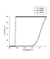
- the operating frequency is changed by 2 MHz from 160 MHz to 258 MHz, and the multiplication operation is executed by the arithmetic circuits L1 and L2 at each operating frequency.
- Fig. 4 shows the relationship between the error rate and the operating frequency in the above verification example.
- the horizontal axis of the graph of FIG. 4 is the operating frequency of the FPGA 10, and the vertical axis is the error occurrence rate.
- the number of error occurrences is counted when at least one of the operation result data V1 and V2 becomes an incorrect value, and the error occurrence rate is calculated based on the input data X for each operating frequency.
- the ratio (%) of the number of error occurrences to the number of inputs (10,000 times). Whether or not the calculation result data V1 and V2 have incorrect values is determined by comparing the true value calculated separately and the calculation result data V1 and V2.
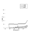
- FIG. 5 shows the error detection rate due to the mismatch between the calculation result data V1 and V2.
- the horizontal axis of the graph of FIG. 5 is the operating frequency of the FPGA 10, and the vertical axis is the error detection rate.
- the number of times of error detection is counted assuming that the calculation result data V1 and V2 do not coincide with each other, and the error detection rate is the number of inputs of the input data X for each operating frequency (1 The ratio (%) of error detection times to (10,000 times).
- FIG. 5 shows the result of verification at an operating frequency of 178 MHz or higher in which an error was detected in Comparative Example 1 described later.
- FIG. 6 shows the distance between the calculation result data V1 and V2 (hereinafter referred to as the mismatch distance).
- the mismatch distance (D) is obtained by dividing the sum of error bits normalized by 32 bits by the number of times of error detection at the operating frequency for each operating frequency. Indicated by The mismatch distance increases when the difference between the calculation result data V1 and V2 is large.
- E (i, f) in the above equation (1) is the number of bits that do not match between the operation result data V1 and V2 for the i-th input data X at the operating frequency f.
- S (f) is the number of times of error detection at the operating frequency f.
- Comparative Example 1 a timing simulation for an FPGA in which two arithmetic circuits L1 in which the DSP block 12 is used to the maximum is formed is referred to as Comparative Example 1.
- Comparative Example 2 A timing simulation of an FPGA in which two arithmetic circuits L2 formed by combining circuit blocks are formed is referred to as Comparative Example 2.
- the configuration information for forming the arithmetic circuits L1 and L2 in the FPGAs of Comparative Example 1 and Comparative Example 2 was generated in the same manner as in the verification example. And also about the comparative example 1 and the comparative example 2, the timing simulation was performed on the simulation tool similarly to the verification example.
- the verification results of Comparative Example 1 and Comparative Example 2 are also shown in FIGS.
- Comparative Example 1 From the above, in Comparative Example 1, it can be seen that the operation result data output from at least one of the two operation circuits L1 has an incorrect value at an operating frequency of 178 MHz or higher. However, as shown in FIG. 5, in Comparative Example 1, errors are detected at several operating frequencies of 178 MHz or higher, but errors are not detected at other operating frequencies. This is because, in Comparative Example 1, two arithmetic circuits L1 composed of the same circuit block combination are used, so that the same error occurs in each of the two arithmetic circuits L1, and the respective arithmetic operations to be output This is because the result data is exactly the same and as a result cannot be detected as an error. In Comparative Example 2, the error detection rate is almost 100%, but at the operating frequency above 218 MHz, a decrease in the error detection rate of about 1 to 2% was observed.
- the error detection rate of the verification example according to the present invention was 100% at all operating frequencies. That is, rather than a configuration in which a plurality of arithmetic circuits having the same combination of circuit blocks are made redundant as in Comparative Example 1 and Comparative Example 2, a plurality of arithmetic circuits L1 having different combinations of circuit blocks as in the verification example of the present invention. L2, that is, by using a configuration in which a plurality of arithmetic circuits having diversity are formed, it has been confirmed that errors can be detected more reliably, thus improving the error detection rate. Further, as shown in FIG. 6, it was confirmed that the mismatch distance in the verification example was three times or more larger than that in Comparative Example 1 and Comparative Example 2.
Abstract
The present invention forms arithmetic-operation circuits (L1-L3) and a verification circuit (21) by loading configuration information into configuration memory of an FPGA (10). Although the arithmetic-operation circuits (L1-L3) have the same arithmetic operating function, they differ from one another in their circuit block combinations. The arithmetic-operation circuits (L1 and L3) have a combination of circuit blocks in which the maximum number of DSP blocks (12) are used, and the arithmetic-operation circuit (L2) has a combination of circuit blocks including no DSP blocks (12). The arithmetic-operation circuits (L1 and L2) use a block RAM (13) as data storage memory, and the arithmetic-operation circuit (L3) uses a distributed RAM as the data storage memory. Input data (X) is input to each of the arithmetic-operation circuits (L1-L3), which output arithmetic-operation result data (V1-V3). The verification circuit (21) compares the arithmetic-operation result data (V1-V3) and verifies whether there is an error.
Description
本発明は、プログラマブルロジックデバイス、プログラマブルロジックデバイスのエラー検証方法、及びプログラマブルロジックデバイスの回路形成方法に関するものである。
The present invention relates to a programmable logic device, a programmable logic device error verification method, and a programmable logic device circuit formation method.
近年において、プログラマブルロジックデバイス、特にFPGA(Field Programmable Gate Array)は、制御や通信の分野で多く使われるようになってきた。FPGAは、FPGA内の構成メモリに構成情報をロードすることにより、基本論理ブロック(CLB(Configurable Logic Block)、LE(Logic Element)等とも称される)等の回路ブロックを組み合わせることによって演算回路を形成する。演算回路としては、単純な数値演算を行うものからCPU(Central Processing Unit)に相当する機能を有するものまで様々なものを実現可能である(例えば、特許文献1参照)。
In recent years, programmable logic devices, especially FPGA (Field Programmable Gate Array) have come to be widely used in the field of control and communication. The FPGA loads the configuration information into the configuration memory in the FPGA, thereby combining arithmetic circuit by combining circuit blocks such as basic logic blocks (also called CLB (Configurable Logic Block), LE (Logic Element), etc.). Form. Various arithmetic circuits can be realized, ranging from those that perform simple numerical operations to those that have a function corresponding to a CPU (Central Processing Unit) (for example, see Patent Document 1).
FPGAでは、演算機能を実現する1つ1つの演算が回路ブロックに対応しており、当該回路ブロックの組み合わせが変更されることにより様々な演算機能が実現されている。このため、FPGAでは、演算機能の演算数の増大にともなって、演算回路に使用される回路ブロックの数も多くなる。この結果、FPGAでは、回路ブロックの数が多い複雑な演算回路が形成されると、当該演算回路に使用する回路ブロックの数の増加に伴い、演算回路に使用される回路ブロック内のANDゲートやORゲート等の回路素子の数も多くなる。
In the FPGA, each calculation that realizes a calculation function corresponds to a circuit block, and various calculation functions are realized by changing the combination of the circuit blocks. For this reason, in the FPGA, the number of circuit blocks used in the arithmetic circuit increases as the number of arithmetic functions increases. As a result, in a FPGA, when a complex arithmetic circuit having a large number of circuit blocks is formed, an AND gate in the circuit block used for the arithmetic circuit is increased as the number of circuit blocks used for the arithmetic circuit increases. The number of circuit elements such as OR gates also increases.
ここで、これらANDゲートやORゲート等の回路素子は、大気中の荷電粒子等の影響を受けて誤作動することもある。そして、例えば演算回路に組み込まれた回路素子が誤作動した場合には、当該演算回路の演算結果がエラーとなる。そのため、FPGAでは、演算回路に使用する回路素子の数が多くなると、当該回路素子の数が多くなる分、大気中の荷電粒子等の影響を受ける確率も高くなり、エラーが発生する恐れが高くなるという問題がある。
Here, circuit elements such as AND gates and OR gates may malfunction due to the influence of charged particles in the atmosphere. For example, when a circuit element incorporated in the arithmetic circuit malfunctions, an arithmetic result of the arithmetic circuit becomes an error. Therefore, in an FPGA, when the number of circuit elements used in an arithmetic circuit increases, the number of circuit elements increases, so the probability of being affected by charged particles in the atmosphere increases, and there is a high risk of errors. There is a problem of becoming.
また、上記のようなFPGAでは、例えばFPGAを駆動するクロックの変動や、FPGAの電源の電圧変動、FPGA自体の温度変動に対するロバスト性が、回路ブロック間を接続する配線の状態(接続状態)によって左右されることが知られており、演算回路を構成する回路ブロック間の接続状態によっては、エラーが発生し易くなるという問題もある。
Further, in the FPGA as described above, for example, robustness against fluctuations in the clock driving the FPGA, voltage fluctuations in the power supply of the FPGA, and temperature fluctuations in the FPGA itself depends on the state of the wiring (connection state) connecting the circuit blocks. It is known that it depends on each other, and there is a problem that an error is likely to occur depending on the connection state between circuit blocks constituting the arithmetic circuit.
そこで、従来では、同じ種類の回路ブロックを組み合わせて同じ演算処理を行う演算回路を2重、3重にFPGA内に設け、このように冗長化された各演算回路で同時に同じ演算を行って、各演算回路の演算結果を比較し、いずれかの演算回路で回路ブロックが誤作動しているか否か、すなわち演算結果にエラーがあるか否かを検証するエラー検証方法を行うことが考えられている。
Therefore, conventionally, arithmetic circuits that perform the same arithmetic processing by combining the same types of circuit blocks are provided in the FPGA in double and triple, and the same arithmetic is simultaneously performed in each redundant arithmetic circuit in this manner, It is conceivable to perform an error verification method that compares the calculation results of each calculation circuit and verifies whether the circuit block is malfunctioning in any calculation circuit, that is, whether the calculation result has an error. Yes.
ところで、従来のエラー検証方法では、同じ種類の回路ブロックを組み合わせて同じ演算処理を行う複数の演算回路で、演算回路を冗長化している。このため、FPGA自体の温度変動や、FPGAの電源の電圧変動、FPGAを駆動するクロックの変動等、FPGA全体で共通する要因(以下、共通要因と呼ぶ)に起因したエラーが生じた場合、FPGAの各演算回路から得られる演算結果にエラーが発生しているにもかかわらず、同じ演算結果が得られてしまい、エラーの発生を検知することができない場合もあるという問題があった。そのため、従来のエラー検証方法では、エラー検知率が十分に高いとはいえなかった。
Incidentally, in the conventional error verification method, the arithmetic circuit is made redundant with a plurality of arithmetic circuits that combine the same types of circuit blocks and perform the same arithmetic processing. For this reason, when an error due to a factor common to the entire FPGA (hereinafter referred to as a common factor) such as a temperature variation of the FPGA itself, a voltage variation of the FPGA power supply, a clock variation for driving the FPGA, or the like occurs, In spite of an error occurring in the calculation result obtained from each of the calculation circuits, there is a problem that the same calculation result is obtained and the occurrence of the error cannot be detected in some cases. Therefore, the conventional error verification method cannot be said to have a sufficiently high error detection rate.
本発明は、上記事情に鑑みてなされたものであり、従来よりもエラー検知率を向上させることができるプログラマブルロジックデバイス、プログラマブルロジックデバイスのエラー検証方法、及びプログラマブルロジックデバイスの回路形成方法を提供することを目的とする。
The present invention has been made in view of the above circumstances, and provides a programmable logic device, an error verification method for a programmable logic device, and a circuit formation method for a programmable logic device capable of improving the error detection rate as compared with the conventional technology. For the purpose.
本発明は、複数の回路ブロックの組み合わせを変えることにより、演算機能が変更可能なプログラマブルロジックデバイスにおいて、回路ブロックの組み合わせ及び接続状態が互いに異なり、かつ互いに同じ演算をする第1演算回路及び第2演算回路と、第1演算回路及び第2演算回路のそれぞれに設けられており、演算結果を検証する検証回路に第1演算回路及び第2演算回路の演算結果を出力する出力部とを備えるものである。
The present invention provides a first arithmetic circuit and a second arithmetic circuit that are different in combination and connection state of circuit blocks and perform the same operation in a programmable logic device that can change an arithmetic function by changing a combination of a plurality of circuit blocks. Arithmetic circuit, and provided in each of the first arithmetic circuit and the second arithmetic circuit, the verification circuit for verifying the arithmetic result includes an output unit for outputting the arithmetic result of the first arithmetic circuit and the second arithmetic circuit It is.
また、本発明は、複数の回路ブロックの組み合わせを変えることにより、演算機能が変更可能なプログラマブルロジックデバイスのエラー検証方法において、回路ブロックの組み合わせ及び接続状態が互いに異なり、かつ互いに同じ演算をする第1演算回路及び第2演算回路を形成する回路形成ステップと、第1演算回路及び第2演算回路でそれぞれ演算を行う演算ステップと、第1演算回路及び第2演算回路からの演算結果を検証する検証ステップとを有するものである。
The present invention also relates to an error verification method for a programmable logic device that can change an arithmetic function by changing a combination of a plurality of circuit blocks. A circuit formation step for forming one arithmetic circuit and a second arithmetic circuit, an arithmetic step for performing arithmetic operations in the first arithmetic circuit and the second arithmetic circuit, respectively, and the arithmetic results from the first arithmetic circuit and the second arithmetic circuit are verified. And a verification step.
さらに、本発明は、構成情報にしたがって複数の回路ブロックの組み合わせを変えることにより、演算機能が変更可能なプログラマブルロジックデバイスの回路形成方法において、回路ブロックの組み合わせに関する条件が異なる合成パラメータを順次設定する合成パラメータ設定ステップと、合成パラメータ設定ステップで合成パラメータが設定されるごとに、設定された合成パラメータの下で論理合成を行い、ハードウェア記述言語で記述された同一の演算回路記述情報から複数の演算回路に対応した複数のネットリストを生成する論理合成ステップと、複数のネットリストから構成情報を生成する構成情報生成ステップと、構成情報をプログラマブルロジックデバイスに書き込み、複数のネットリストに対応して、回路ブロックの組み合わせ及び接続状態が互いに異なり、かつ互いに同じ演算をする第1演算回路及び第2演算回路と、第1演算回路及び第2演算回路にそれぞれ設けられ、演算結果を検証する検証回路に第1演算回路及び第2演算回路の演算結果を出力する出力部とをプログラマブルロジックデバイスに形成する形成ステップとを有するものである。
Furthermore, the present invention sequentially sets synthesis parameters having different conditions regarding the combination of circuit blocks in a circuit formation method for a programmable logic device capable of changing an arithmetic function by changing a combination of a plurality of circuit blocks according to configuration information. Each time a synthesis parameter is set in the synthesis parameter setting step and the synthesis parameter setting step, logic synthesis is performed under the set synthesis parameter, and a plurality of arithmetic circuit description information described in the hardware description language are used. A logic synthesis step for generating a plurality of netlists corresponding to the arithmetic circuit, a configuration information generation step for generating configuration information from the plurality of netlists, and writing the configuration information to the programmable logic device, corresponding to the plurality of netlists. A set of circuit blocks The first arithmetic circuit and the second arithmetic circuit that are different from each other in the combination and connection state and perform the same arithmetic operation, and the first arithmetic circuit and the second arithmetic circuit are provided in the first arithmetic circuit and the second arithmetic circuit, respectively. Forming a circuit and an output unit for outputting a calculation result of the second calculation circuit in a programmable logic device.
本発明のプログラマブルロジックデバイス、及びそのエラー検証方法によれば、回路ブロックの組み合わせに応じて、温度変動や電圧変動、クロック変動の共通要因に対する各演算回路での動作状況が異なるため、各演算回路で発生するエラーの発生状態も異なってくることから、従来の単に冗長化した複数の演算回路から得られる演算結果を比較する場合に比べ、各演算回路から得られた演算結果を比較する際に、共通要因に起因したエラーをも検知でき、かくして、従来よりもエラー検知率を向上させることができる。
According to the programmable logic device and the error verification method of the present invention, each arithmetic circuit has different operation states for common factors of temperature fluctuation, voltage fluctuation, and clock fluctuation depending on the combination of circuit blocks. Since the error occurrence state that occurs at the same time also differs, when comparing the calculation results obtained from each calculation circuit, compared to the conventional calculation results obtained from a plurality of redundant calculation circuits. Thus, errors caused by common factors can be detected, and thus the error detection rate can be improved as compared with the conventional case.
また、本発明のプログラマブルロジックデバイスの回路形成方法によれば、複数のネットリストから生成された構成情報をプログラマブルロジックデバイスに適用することによって、同じ演算機能を持ち、かつ回路ブロックの組み合わせが異なる複数の演算回路をそのプログラマブルロジックデバイスに形成できる。これにより、上述した構成情報が適用されたプログラマブルロジックデバイスでは、回路ブロックの組み合わせに応じて、温度変動や電圧変動、クロック変動の共通要因に対する各演算回路での動作状況が異なるため、各演算回路で発生するエラーの発生状態も異なってくることから、従来の単に冗長化した複数の演算回路から得られる演算結果を比較する場合に比べ、各演算回路から得られた演算結果を比較する際に、共通要因に起因したエラーをも検知でき、かくして、従来よりもエラー検知率を向上させることができる。
Further, according to the circuit formation method of the programmable logic device of the present invention, by applying the configuration information generated from a plurality of netlists to the programmable logic device, the plurality of combinations having the same arithmetic function and different circuit blocks are provided. Can be formed in the programmable logic device. As a result, in the programmable logic device to which the above-described configuration information is applied, the operation state of each arithmetic circuit for common factors of temperature fluctuation, voltage fluctuation, and clock fluctuation differs depending on the combination of circuit blocks. Since the error occurrence state that occurs at the same time also differs, when comparing the calculation results obtained from each calculation circuit, compared to the conventional calculation results obtained from a plurality of redundant calculation circuits. Thus, errors caused by common factors can be detected, and thus the error detection rate can be improved as compared with the conventional case.
図1に本実施形態に用いるFPGA(Field Programmable Gate Array)10を示す。本実施形態では、プログラマブルロジックデバイス(PLD)の一例として、一般的なFPGA10に本発明を適用した場合について説明する。FPGA10は、例えば通信処理機能や、暗号化処理機能、画像処理機能等のような演算機能の変更が可能なデバイスである。FPGA10には、演算処理の対象となる信号の種類や演算処理の内容に合わせて所望の演算機能を実現するため、基本論理ブロック11、DSPブロック12、ブロックRAM13、IOブロック(Input/Output Block)14、PLLブロック15等が回路ブロック(回路要素)として設けられている。また、回路ブロックの他に、FPGA10には、構成メモリ16や、回路ブロックの間を繋ぐ配線リソース(図示省略)が設けられている。
FIG. 1 shows an FPGA (Field Programmable Gate Array) 10 used in this embodiment. In the present embodiment, a case where the present invention is applied to a general FPGA 10 will be described as an example of a programmable logic device (PLD). The FPGA 10 is a device that can change arithmetic functions such as a communication processing function, an encryption processing function, and an image processing function. The FPGA 10 includes a basic logic block 11, a DSP block 12, a block RAM 13, an IO block (Input / Output block) in order to realize a desired calculation function in accordance with the type of signal to be calculated and the content of the calculation process. 14, PLL block 15 and the like are provided as circuit blocks (circuit elements). In addition to the circuit blocks, the FPGA 10 is provided with a configuration memory 16 and wiring resources (not shown) for connecting the circuit blocks.
基本論理ブロック11は、FPGA10を構成する基本的な回路ブロックであり、CLB(Configurable Logic Block)、ロジックエレメント(Logic Element)、ロジックセル(Logic Cell)等とも称されるものである。基本論理ブロック11は、種々の構成のものがあるが、一般的にはLUT(Lookup table)とレジスタ(フリップフロップ)を基本要素とする複数の基本回路(スライス等と称される場合もある)から構成されている。
The basic logic block 11 is a basic circuit block constituting the FPGA 10, and is also referred to as a CLB (Configurable Logic Block), a logic element (Logic Element), a logic cell (Logic Cell), or the like. The basic logic block 11 has various configurations, but in general, a plurality of basic circuits having a LUT (Lookup table) and a register (flip-flop) as basic elements (sometimes referred to as a slice or the like). It is composed of
DSPブロック12は、基本論理ブロック11の組み合わせではなく、乗算や積和演算等の演算を高速に処理するためにハードウェア(ハードマクロ)として予め組み込まれている回路ブロックであり、DSPスライス12等と称される場合もある。このDSPブロック12は、高速な乗算器と加算器を基本要素として構成されている。ブロックRAM13は、一般的なメモリとして利用可能な回路ブロックである。ブロックRAM13は、例えば他の回路ブロックから出力される演算途中のデータを一時的に保持する際に利用される。IOブロック14は、FPGA10の入力機能及び出力機能を提供する回路ブロックである。PLLブロック15は、回路ブロックの動作に必要なクロックを発生する。配線リソースは、回路ブロック同士を接続する配線及び配線上に設けられたパストランジスタで構成されている。
The DSP block 12 is not a combination of the basic logic blocks 11, but is a circuit block that is incorporated in advance as hardware (hardware macro) in order to process operations such as multiplication and product-sum operations at high speed. Sometimes called. The DSP block 12 is composed of a high-speed multiplier and adder as basic elements. The block RAM 13 is a circuit block that can be used as a general memory. The block RAM 13 is used, for example, when temporarily storing data that is being output from other circuit blocks. The IO block 14 is a circuit block that provides an input function and an output function of the FPGA 10. The PLL block 15 generates a clock necessary for the operation of the circuit block. The wiring resource is composed of a wiring connecting circuit blocks and a pass transistor provided on the wiring.
構成メモリ16には、構成情報18がロード(書き込み)される。構成情報18は、回路ブロックの動作や、配線リソースによる回路ブロック間の接続等を定義するものであり、コンフィギュレーション・データ、ビットストリーム等と称されるものである。FPGA10には、この構成情報18にしたがって、所望する演算回路が形成される。すなわち、FPGA10は、構成情報18にしたがって複数の回路ブロックの組み合わせが変更され、これにより演算機能が変更可能なデバイスとなっている。
Configuration information 18 is loaded (written) into the configuration memory 16. The configuration information 18 defines the operation of the circuit block, the connection between the circuit blocks by wiring resources, and is called configuration data, a bit stream, or the like. A desired arithmetic circuit is formed in the FPGA 10 according to the configuration information 18. In other words, the FPGA 10 is a device in which the combination of a plurality of circuit blocks is changed in accordance with the configuration information 18 and the arithmetic function can be changed thereby.
FPGA10は、同じ演算機能を持ち、かつ回路ブロックの組み合わせ及び接続状態が異なる複数の演算回路を形成させる構成情報18が構成メモリ16にロードされることにより、当該構成情報18にしたがって、図2に示すように、例えば演算回路L1~L3と検証回路21とが形成される。すなわち、FPGA10には、少なくとも第1演算回路と第2演算回路とが形成される。また、演算回路L1~L3には、演算結果を検証する検証回路21に、対応する演算回路の演算結果を出力する出力部L1a~L3aがそれぞれ形成される。なお、この例では、3個の演算回路L1~L3の場合について説明するが、演算回路は2個以上あればよい。また、構成情報18は、外部のコンピュータから構成メモリ16にロードしたり、構成情報18が予め書き込まれた不揮発性メモリから自動的にロードしたりしてもよい。
The FPGA 10 loads the configuration information 18 having the same calculation function and forms a plurality of calculation circuits having different combinations and connection states of circuit blocks into the configuration memory 16. As shown, for example, arithmetic circuits L1 to L3 and a verification circuit 21 are formed. That is, at least a first arithmetic circuit and a second arithmetic circuit are formed in the FPGA 10. Further, in the arithmetic circuits L1 to L3, output units L1a to L3a for outputting the operation results of the corresponding operation circuits are formed in the verification circuit 21 for verifying the operation results, respectively. In this example, the case of three arithmetic circuits L1 to L3 will be described, but two or more arithmetic circuits may be used. The configuration information 18 may be loaded into the configuration memory 16 from an external computer, or may be automatically loaded from a nonvolatile memory in which the configuration information 18 is written in advance.
図2に示すように、この例におけるFPGA10には、p(p≧1)ビットの入力データX(x1~xp)が入力される。例えば機器(図示省略)の動作を制御する制御システムにFPGA10が設けられ、機器の動作を監視するセンサ(図示省略)からの検出値等が入力データXとしてFPGA10に入力される場合について以下に説明する。なお、入力データXは、1つの値を表すものに限定されない。例えば、複数の検出値をまとめて入力データXとしてもよい、この場合には複数の検出値のビット数の合計がpビットとなる。また、入力データXは、例えばコンピュータ等で生成された1組あるいは複数組の数値、ネットワークを介して受信したデータ、各種機器の駆動を制御するタイミング信号等であってもよい。
As shown in FIG. 2, p (p ≧ 1) -bit input data X (x 1 to x p ) is input to the FPGA 10 in this example. For example, a case where the FPGA 10 is provided in a control system that controls the operation of a device (not shown), and a detection value from a sensor (not shown) that monitors the operation of the device is input to the FPGA 10 as input data X will be described below. To do. The input data X is not limited to representing one value. For example, a plurality of detection values may be combined into the input data X. In this case, the total number of bits of the plurality of detection values is p bits. Further, the input data X may be, for example, one or more sets of numerical values generated by a computer, data received via a network, timing signals for controlling driving of various devices, and the like.
上述の入力データXは、FPGA10内で演算回路L1~L3にそれぞれ入力される。演算回路L1は、入力データXが入力されると、所定の演算を行って、q(q≧1)ビットの演算結果データV1(v11~v1q)を出力する。演算回路L2、L3についても同じであり、入力データXが入力されると、所定の演算を行って、演算結果データV2(v21~v2q)、V3(v31~v3q)を出力する。
The above input data X is input to the arithmetic circuits L1 to L3 in the FPGA 10, respectively. When the input data X is input, the arithmetic circuit L1 performs a predetermined operation and outputs q (q ≧ 1) bits of operation result data V1 (v 11 to v 1q ). The same applies to the arithmetic circuits L2 and L3. When the input data X is input, a predetermined calculation is performed, and calculation result data V2 (v 21 to v 2q ) and V3 (v 31 to v 3q ) are output. .
演算回路L1~L3は、同じ演算機能を持つが、エラー検知率を向上させるために、回路ブロックの組み合わせ及び接続状態を互いに異なるものにしている。すなわち、演算回路L1~L3は、使用する回路ブロックの種類や数、回路ブロック内でのLUTやレジスタの使われ方、これら回路ブロックの接続状態が演算回路L1~L3では互いに異なったものになっているが、演算回路L1~L3にエラーが発生しない状態では、演算回路L1~L3は、同一の入力データXの入力に応答して同じ演算結果データV1~V3を出力するよう構成されている。回路ブロックの組み合わせ及び接続状態が互いに異なるという観点からは、演算回路L1~L3は、相互に第1演算回路と第2演算回路の関係にある。
The arithmetic circuits L1 to L3 have the same arithmetic function, but in order to improve the error detection rate, the combinations and connection states of the circuit blocks are different from each other. That is, the arithmetic circuits L1 to L3 have different types and numbers of circuit blocks to be used, how to use LUTs and registers in the circuit blocks, and the connection states of these circuit blocks in the arithmetic circuits L1 to L3. However, when no error occurs in the arithmetic circuits L1 to L3, the arithmetic circuits L1 to L3 are configured to output the same arithmetic result data V1 to V3 in response to the input of the same input data X. . From the viewpoint that the combination and connection state of the circuit blocks are different from each other, the arithmetic circuits L1 to L3 are in a relationship between the first arithmetic circuit and the second arithmetic circuit.
上記のように演算回路L1~L3の回路ブロックの組み合わせを互いに異なるものにすることによって、演算回路L1~L3が同時にエラーを発生させる可能性を低くするとともに、また演算回路L1~L3が同時にエラーを発生させても各演算結果データV1~V3が同じになる可能性を極めて低くしている。
By making the combinations of the circuit blocks of the arithmetic circuits L1 to L3 different from each other as described above, it is possible to reduce the possibility that the arithmetic circuits L1 to L3 will generate errors at the same time, and the arithmetic circuits L1 to L3 will simultaneously generate errors. Even if this occurs, the possibility that the calculation result data V1 to V3 are the same is extremely reduced.
例えば、演算回路L1、L3は、組み合わされる複数の回路ブロックの中に少なくとも1つ以上のDSPブロック12が含まれた回路構成を有している。一方、演算回路L2は、DSPブロック12以外の回路ブロックが組み合わされた回路構成(例えば、LUTを含む基本論理ブロック11を主体とした回路構成)を有している。したがって、DSPブロック12を含む回路構成であるか否かの観点からは、演算回路L1、L3は、第1演算回路に相当し、演算回路L2は、第2演算回路に相当する。また、演算回路L1と演算回路L2とは、例えば演算中のデータを保持するメモリ(以下、データ保持メモリ)として、ブロックRAM13を使用するのに対して、演算回路L3は、基本論理ブロック11のフリップフロップを利用したいわゆる分散RAMを使用する回路ブロックの組み合わせである。このようにして、演算回路L1~L3は、種類の異なる回路ブロックを用い、相互に回路ブロックの組み合わせが異なるものになっており、多様性のあるものとなっている。
For example, the arithmetic circuits L1 and L3 have a circuit configuration in which at least one DSP block 12 is included in a plurality of circuit blocks to be combined. On the other hand, the arithmetic circuit L2 has a circuit configuration in which circuit blocks other than the DSP block 12 are combined (for example, a circuit configuration mainly including the basic logic block 11 including the LUT). Therefore, from the viewpoint of whether or not the circuit configuration includes the DSP block 12, the arithmetic circuits L1 and L3 correspond to the first arithmetic circuit, and the arithmetic circuit L2 corresponds to the second arithmetic circuit. The arithmetic circuit L1 and the arithmetic circuit L2 use, for example, a block RAM 13 as a memory for holding data being calculated (hereinafter referred to as a data holding memory), whereas the arithmetic circuit L3 has a basic logic block 11 configuration. This is a combination of circuit blocks using a so-called distributed RAM using flip-flops. In this way, the arithmetic circuits L1 to L3 use different types of circuit blocks, and the combinations of the circuit blocks are different from each other.
演算回路L1、L3のようにDSPブロック12を使用した場合には、演算回路L2のようにDSPブロック12を使用しない場合に比べて、使用される基本論理ブロック11の個数を大幅に少なくさせることもでき、回路ブロック間を接続した配線の長さも含め演算回路を形成する回路ブロック11の組み合わせを大きく異ならせることができる。すなわち、演算回路L1、L3と演算回路L2とは、論理的な演算機能は同じであるが、ゲートレベルにおける動作(信号処理の物理的プロセスや、物性レベルの素子内部の振る舞い等)が大きく異なり、FPGA10の温度変動や電圧変動、クロック変動等の共通要因がゲートレベルにおける動作に与える影響も大きく異なってくる。このため、FPGA10では、上記共通要因に対する演算回路L1、L3と演算回路L2とのゲートレベルにおける動作状況が大きく異なるため、エラー発生時の演算結果データの不一致の程度も大きくなることが期待できる。したがって、DSPブロック12の使用の有無によって回路ブロック11の組み合わせを異なったものとすることは、エラーの発生を演算結果データの不一致によって検知する際に非常に有利である。
When the DSP block 12 is used like the arithmetic circuits L1 and L3, the number of the basic logic blocks 11 used is greatly reduced compared to the case where the DSP block 12 is not used like the arithmetic circuit L2. In addition, the combination of the circuit blocks 11 forming the arithmetic circuit including the length of the wiring connecting the circuit blocks can be greatly varied. That is, the arithmetic circuits L1 and L3 and the arithmetic circuit L2 have the same logical arithmetic function, but the operation at the gate level (physical process of signal processing, behavior inside the element at the physical property level, etc.) is greatly different. The influence of common factors such as temperature fluctuation, voltage fluctuation and clock fluctuation of the FPGA 10 on the operation at the gate level is also greatly different. For this reason, in the FPGA 10, the operation states at the gate levels of the arithmetic circuits L1 and L3 and the arithmetic circuit L2 with respect to the common factor are greatly different, so that it can be expected that the degree of inconsistency of the arithmetic result data at the time of error occurrence also increases. Therefore, making the combination of the circuit blocks 11 different depending on whether or not the DSP block 12 is used is very advantageous when detecting the occurrence of an error based on the mismatch of operation result data.
この実施の形態の場合、FPGA10には、複数の回路ブロックが組み合わされることにより検証回路21が形成されている。演算回路L1~L3は、出力部L1a~L3aが演算結果データV1~V3を検証回路21に送る。検証回路21は、演算結果データV1~V3を検証し、その検証結果として検証データRを生成する。また、検証回路21は、演算結果データV1~V3のうちエラーがないと推測すると、演算結果データとして出力データY(y1~yq)を生成する。この検証回路21は、検証データRと出力データYとを制御システムのシステムコントローラ(図示省略)に出力する。
In the case of this embodiment, the verification circuit 21 is formed in the FPGA 10 by combining a plurality of circuit blocks. In the arithmetic circuits L1 to L3, the output units L1a to L3a send the operation result data V1 to V3 to the verification circuit 21. The verification circuit 21 verifies the operation result data V1 to V3, and generates verification data R as the verification result. Further, when the verification circuit 21 estimates that there is no error among the calculation result data V1 to V3, the verification circuit 21 generates output data Y (y 1 to y q ) as calculation result data. The verification circuit 21 outputs verification data R and output data Y to a system controller (not shown) of the control system.
上記検証回路21は、例えば多数決方式によって出力データYを決定する。すなわち、演算結果データV1~V3の値を比較して一致、不一致を判定し、同じ値となっている演算結果データの個数が最も多い演算結果データを正常値とし、その正常値を出力データYとして出力する。
The verification circuit 21 determines the output data Y by, for example, a majority method. That is, the values of the operation result data V1 to V3 are compared to determine whether they match or not, and the operation result data with the largest number of operation result data having the same value is set as a normal value, and the normal value is output data Y Output as.
FPGA10は、例えば演算回路L1~L3のいずれもがエラーを発生していないときには、演算回路L1~L3から得られる各演算結果データV1~V3が全て一致する。また、演算回路L1~L3のうち例えば演算回路L1だけにエラーが発生しているときには、演算回路L2,L3から得られる演算結果データV2、V3と、演算回路L1から得られる演算結果データV1とが異なるものとなる。また、演算回路L1~L3のうち例えば演算回路L2,L3にだけエラーが発生しているとき、演算回路L2,L3から得られる演算結果データV2、V3と、演算回路L1から得られる演算結果データV1とが異なるものとなる。
In the FPGA 10, for example, when none of the arithmetic circuits L1 to L3 generates an error, the arithmetic result data V1 to V3 obtained from the arithmetic circuits L1 to L3 all match. Further, when an error occurs only in the arithmetic circuit L1 among the arithmetic circuits L1 to L3, for example, the arithmetic result data V2 and V3 obtained from the arithmetic circuits L2 and L3, and the arithmetic result data V1 obtained from the arithmetic circuit L1 Will be different. Further, for example, when an error occurs only in the arithmetic circuits L2 and L3 among the arithmetic circuits L1 to L3, the arithmetic result data V2 and V3 obtained from the arithmetic circuits L2 and L3 and the arithmetic result data obtained from the arithmetic circuit L1 V1 is different.
さらに、FPGA10は、前述のように演算回路L1~L3を回路ブロックの組み合わせが互いに異なる回路構成とすることによって、温度変動や電圧変動、クロック変動の共通要因でエラーが発生しても、当該共通要因に対する各演算回路L1~L3での動作状況が異なるので、演算回路L1~L3から得られる各演算結果データV1~V3が互いに異なるものとなる。
Further, the FPGA 10 has a circuit configuration in which the combinations of the circuit blocks are different from each other in the arithmetic circuits L1 to L3 as described above, so that even if an error occurs due to a common factor of temperature fluctuation, voltage fluctuation, and clock fluctuation, Since the operation states in the operation circuits L1 to L3 with respect to the factors are different, the operation result data V1 to V3 obtained from the operation circuits L1 to L3 are different from each other.
これにより、FPGA10では、演算回路L1~L3から得られる各演算結果データV1~V3が全て一致するときFPGA10にエラーが発生していないと判断でき、一方、演算回路L1~L3から得られる各演算結果データV1~V3が不一致のときFPGA10にエラーが発生していると判断し得る。
As a result, the FPGA 10 can determine that no error has occurred in the FPGA 10 when all the operation result data V1 to V3 obtained from the operation circuits L1 to L3 match, and each operation obtained from the operation circuits L1 to L3. When the result data V1 to V3 do not match, it can be determined that an error has occurred in the FPGA 10.
検証データRは、エラーの発生状況や出力データYの確からしさの判断の指標となる情報である。この例では、検証データRは、演算結果データV1~V3に対応した個別検証データR1~R3を含んでいる。個別検証データR1~R3は、例えば出力データYを正常値としたときに、対応する演算結果データV1~V3の誤りビットの個数、何ビット目が誤りビットになっているか、出力データYに示される値と演算結果データとの差等の情報を有したものとなっている。システムコントローラは、このような個別検証データR1~R3を含む検証データRにより、正常値と不一致となっている演算結果データの個数や不一致の演算結果データ中のビット数、エラーが発生したと推測される演算回路がいずれか、不一致となっている演算結果データの値と正常値との差や、その差の最大値、最小値、幅等の情報を取得できる。
The verification data R is information that serves as an index for determining the error occurrence status and the accuracy of the output data Y. In this example, the verification data R includes individual verification data R1 to R3 corresponding to the operation result data V1 to V3. The individual verification data R1 to R3 indicate in the output data Y, for example, the number of error bits in the corresponding operation result data V1 to V3 and the number of error bits when the output data Y is a normal value. It has information such as the difference between the calculated value and the calculation result data. Based on the verification data R including the individual verification data R1 to R3, the system controller estimates that the number of calculation result data that does not match the normal value, the number of bits in the mismatch calculation result data, and an error have occurred. Any of the operation circuits to be obtained can acquire information such as the difference between the value of the calculation result data and the normal value that are inconsistent, and the maximum value, minimum value, width, etc. of the difference.
図3において、FPGA10にロードされる構成情報18は、構成情報生成装置24によって生成される。この構成情報生成装置24は、回路記述情報26から構成情報18を生成する。回路記述情報26は、レジスタ転送レベル(Register transfer level, RTL)で抽象化した演算機能の仕様を、ハードウェア記述言語(HDL)を用いて記述したものである。この例においては、回路記述情報26は、検証回路21に対応して記述された検証回路記述情報26aと、演算回路記述情報26bとがあり、複数の演算回路L1~L3(図2)に対しては1つの演算回路記述情報26bを共通に使用している。なお、産業用アプリケーションとして使われているFBD(ファンクション ブロック ダイアグラム:Function Block Diagram)言語等を用いて記述され、抽象度をより高くした動作レベル(behavioral level)のハードウェア記述情報に高位合成を行って、レジスタ転送レベルの回路記述情報26を生成してもよい。
3, the configuration information 18 loaded into the FPGA 10 is generated by the configuration information generation device 24. The configuration information generation device 24 generates configuration information 18 from the circuit description information 26. The circuit description information 26 is a description of arithmetic function specifications abstracted at a register transfer level (Register transfer level, RTL) using a hardware description language (HDL). In this example, the circuit description information 26 includes verification circuit description information 26a described corresponding to the verification circuit 21 and arithmetic circuit description information 26b. For the plurality of arithmetic circuits L1 to L3 (FIG. 2), For example, one arithmetic circuit description information 26b is commonly used. It is described using FBD (Function Block Diagram) language used for industrial applications, etc., and high-level synthesis is performed on hardware description information with higher abstraction level (behavioral level). Then, the circuit description information 26 at the register transfer level may be generated.
構成情報生成装置24は、論理合成部24a、合成パラメータ設定部24b、結合部24c、及びマッピング部24dを備えている。例えば、論理合成部24a、結合部24c、及びマッピング部24dは、論理合成ツール等として知られているアプリケーションプログラムをコンピュータにインストールすることで実現される。合成パラメータ設定部24bは、論理合成ツールの論理合成に関する合成パラメータを変更するように構成されている。合成パラメータは、FPGA10に演算回路L1~L3を形成させる際の条件を指定するものであり、この合成パラメータにより回路ブロックの組み合わせに関する条件を変えることができる。
The configuration information generation device 24 includes a logic synthesis unit 24a, a synthesis parameter setting unit 24b, a combining unit 24c, and a mapping unit 24d. For example, the logic synthesis unit 24a, the coupling unit 24c, and the mapping unit 24d are realized by installing an application program known as a logic synthesis tool or the like in a computer. The synthesis parameter setting unit 24b is configured to change a synthesis parameter related to logic synthesis of the logic synthesis tool. The synthesis parameter specifies conditions for forming the arithmetic circuits L1 to L3 in the FPGA 10, and the conditions regarding the combination of circuit blocks can be changed by the synthesis parameters.
論理合成部24aは、回路記述情報26からネットリストを生成する論理合成を行う。ネットリストは、回路ブロック間を接続する配線等を記述したものである。合成パラメータ設定部24bは、論理合成部24aが論理合成する際に、パラメータセットP0~P3を設定する。パラメータセットP0は、検証回路21について回路ブロックの組み合わせが最適になるように設定された複数の合成パラメータを1セットにしたものである。このパラメータセットP0は、検証回路記述情報26aから検証回路21のネットリストN0を生成する際に使用される。
The logic synthesis unit 24 a performs logic synthesis for generating a net list from the circuit description information 26. The netlist describes the wiring and the like for connecting the circuit blocks. The synthesis parameter setting unit 24b sets parameter sets P 0 to P 3 when the logic synthesis unit 24a performs logic synthesis. The parameter set P 0 is a set of a plurality of synthesis parameters set so that the combination of circuit blocks is optimized for the verification circuit 21. This parameter set P 0 is used when generating the net list N 0 of the verification circuit 21 from the verification circuit description information 26a.
また、パラメータセットP1~P3は、いずれも演算回路記述情報26bを回路ブロックの組み合わせに具現化する際の複数の合成パラメータを1セットにしたものである。これらパラメータセットP1~P3は、上述のように回路ブロックの組み合わせが互いに異なる演算回路L1~L3を、同一の演算回路記述情報26bから生成されるようにするために、いくつかの合成パラメータの設定が異なったものになっている。
Also, each of the parameter sets P 1 to P 3 is a set of a plurality of synthesis parameters when the arithmetic circuit description information 26b is embodied in a combination of circuit blocks. These parameter sets P 1 to P 3 include several synthesis parameters in order to generate the arithmetic circuits L1 to L3 having different combinations of circuit blocks as described above from the same arithmetic circuit description information 26b. The settings are different.
この例においては、パラメータセットP1~P3は、DSPブロック12の使用に関する合成パラメータ(以下、DSPパラメータという)とデータ保持メモリに関する合成パラメータ(以下、メモリパラメータという)とを含んでおり、これらの設定値の組み合わせが互いに異なるものになっている。
In this example, the parameter sets P 1 to P 3 include synthesis parameters relating to the use of the DSP block 12 (hereinafter referred to as DSP parameters) and synthesis parameters relating to the data holding memory (hereinafter referred to as memory parameters). The combinations of setting values are different from each other.
パラメータセットP1は、演算回路L1のネットリストN1を生成するためのものである。このパラメータセットP1のDSPパラメータは、DSPブロック12を最大限使用する設定値になっている。また、パラメータセットP1のメモリパラメータは、データ保持メモリとしてブロックRAM13を使用する設定値になっている。パラメータセットP2は、演算回路L2のネットリストN2を生成するためのものである。このパラメータセットP2のDSPパラメータは、DSPブロック12を使用しない設定値であり、またメモリパラメータは、データ保持メモリとしてブロックRAM13を使用する設定値になっている。さらに、パラメータセットP3は、演算回路L3のネットリストN3を生成するためのものである。このパラメータセットP3のDSPパラメータは、DSPブロック12を最大限使用する設定値であり、またメモリパラメータは、データ保持メモリとして分散RAMを使用する設定値になっている。
Parameter set P 1 is for generating the netlist N 1 arithmetic circuit L1. The DSP parameter of the parameter set P 1 is a setting value that uses the DSP block 12 to the maximum extent. The memory parameter in the parameter set P 1 is adapted to set value using the block RAM13 as data memory. Parameter set P 2 is for generating a netlist N 2 arithmetic circuit L2. DSP parameters of this parameter set P 2 is the set value without using the DSP block 12, also a memory parameter is adapted to set value using the block RAM13 as data memory. Furthermore, the parameter set P 3 is for generating a netlist N 3 of the arithmetic circuit L3. DSP parameters of this parameter set P 3 is a set value for maximum use of the DSP block 12, also a memory parameter is adapted to set value using distributed RAM as data memory.
上記のように合成パラメータ設定部24bは、演算回路L1~L3についての論理合成の際に、パラメータセットP1~P3を論理合成部24aに設定することによって、演算回路L1~L3を形成する回路ブロック(FPGAのリソース)の組み合わせに関する条件を与え、演算回路L1~L3の回路ブロックの組み合わせを互いに異なるものとして、演算回路L1~L3に多様性を付与する。
As described above, the synthesis parameter setting unit 24b sets the parameter sets P 1 to P 3 in the logic synthesis unit 24a during logic synthesis for the operation circuits L1 to L3, thereby forming the operation circuits L1 to L3. Conditions relating to the combination of circuit blocks (FPGA resources) are given, and the circuit blocks of the arithmetic circuits L1 to L3 are made different from each other to give diversity to the arithmetic circuits L1 to L3.
論理合成部24aは、合成パラメータセットP0の下で論理合成を行うことによって、検証回路記述情報26aからネットリストN0を生成する。また、論理合成部24aは、合成パラメータセットP1~P3の下で、演算回路記述情報26bを用いた論理合成をそれぞれ行うことによって、ネットリストN1~N3を生成する。
Logic synthesis unit 24a, by performing logic synthesis under composition parameter set P 0, to generate a net list N 0 from the verification circuit description information 26a. In addition, the logic synthesis unit 24a generates netlists N 1 to N 3 by performing logic synthesis using the operation circuit description information 26b under the synthesis parameter sets P 1 to P 3 , respectively.
なお、演算回路L1~L3は、回路ブロックの組み合わせが互いに異なっているため、演算回路L1~L3の相互間で、同じタイミングで入力データXを入力しても、演算結果データV1~V3の出力タイミングが異なる場合がある。このような場合には、検証回路21に対する演算結果データV1~V3の入力タイミングが同時になるように、例えば遅延回路を形成すればよい。
Since the arithmetic circuits L1 to L3 have different combinations of circuit blocks, even if the input data X is input at the same timing between the arithmetic circuits L1 to L3, the operation result data V1 to V3 are output. Timing may be different. In such a case, for example, a delay circuit may be formed so that the input timing of the operation result data V1 to V3 to the verification circuit 21 is the same.
結合部24cは、論理合成部24aから得られる4個のネットリストN0~N3を1つのネットリストに結合する。この結合の際には、結合部24cによって、ネットリストN1~N3に示される3組の出力端子を、ネットリストN0の3組の入力端子に接続したネットリストを生成する。
The combining unit 24c combines the four net lists N 0 to N 3 obtained from the logic synthesis unit 24a into one net list. At the time of this combination, the combining unit 24c generates a net list in which three sets of output terminals shown in the net lists N 1 to N 3 are connected to three sets of input terminals of the net list N 0 .
マッピング部24dは、結合部24cからのネットリストにしたがい、ネットリストに示される接続をFPGA10の回路ブロックや入出力ピンに割り当てるいわゆるマッピング(配置配線)を行う。このマッピング部24dは、マッピングした情報を構成情報18としてFPGA10の構成メモリ16に出力する。構成情報18には、検証回路21を形成するための検証回路構成情報C0と、演算回路L1~L3を形成するための演算回路構成情報C1~C3とが含まれる。
The mapping unit 24d performs so-called mapping (placement wiring) that allocates connections shown in the net list to circuit blocks and input / output pins of the FPGA 10 according to the net list from the coupling unit 24c. The mapping unit 24 d outputs the mapped information as configuration information 18 to the configuration memory 16 of the FPGA 10. The configuration information 18 includes verification circuit configuration information C 0 for forming the verification circuit 21 and arithmetic circuit configuration information C 1 to C 3 for forming the arithmetic circuits L1 to L3.
次に上記構成の作用について説明する。まず、検証回路記述情報26aと、演算回路L1~L3に共通な演算回路記述情報26bとを用意し、これらに基づいて構成情報生成装置24で構成情報18を生成する。例えば、合成パラメータ設定部24bは、最初に論理合成部24aにパラメータセットP0を設定する。この後に、論理合成部24aは、検証回路記述情報26aを読み込み、パラメータセットP0の下で論理合成を行い、検証回路記述情報26aからネットリストN0を生成する。
Next, the operation of the above configuration will be described. First, the verification circuit description information 26a and the arithmetic circuit description information 26b common to the arithmetic circuits L1 to L3 are prepared, and the configuration information generation device 24 generates the configuration information 18 based on these. For example, synthesis parameter setting unit 24b sets a parameter set P 0 to the first logical combining unit 24a. Thereafter, logic synthesis unit 24a reads the verification circuit description information 26a, performs logical synthesis under the parameter set P 0, to generate a net list N 0 from the verification circuit description information 26a.
ネットリストN0の生成後、合成パラメータ設定部24bは、論理合成部24aにパラメータセットP1を設定する。この後、論理合成部24aは、演算回路記述情報26bを読み込み、パラメータセットP1の下で論理合成を行って、演算回路記述情報26bからネットリストN1を生成する。このときに、パラメータセットP1のDSPパラメータは、DSPブロック12を最大限使用する設定値であり、メモリパラメータは、データ保持メモリとしてブロックRAM13を使用する設定値になっている。したがって、所定の演算機能を実現させる演算回路記述情報26bは、パラメータセットP1の下で、DSPブロック12を最大限使用し、かつデータ保持メモリとしてブロックRAM13を使用するする回路ブロックの組み合わせのネットリストN1に変換される。
After generating the netlist N 0, the synthesis parameter setting unit 24b, sets a parameter set P 1 to the logic synthesizing section 24a. Thereafter, logic synthesis unit 24a reads the arithmetic circuit description information 26b, by performing logic synthesis under parameter set P 1, to generate a net list N 1 from the arithmetic circuit description information 26b. At this time, the DSP parameter of the parameter set P 1 is a setting value that uses the DSP block 12 as much as possible, and the memory parameter is a setting value that uses the block RAM 13 as a data holding memory. Accordingly, the arithmetic circuit description information 26b to realize a predetermined calculation function, the parameters under set P 1, the DSP block 12 maximally used, and the net combination of circuit blocks using block RAM13 as data memory It is converted to a list N 1.
ネットリストN1の生成後、論理合成部24aには、合成パラメータ設定部24bによってパラメータセットP2が設定される。この後、論理合成部24aは、演算回路記述情報26bを読み込み、パラメータセットP2の下で論理合成を行って、この演算回路記述情報26bからネットリストN2を生成する。パラメータセットP2の場合は、DSPパラメータがDSPブロック12を使用しない設定値であり、メモリパラメータがデータ保持メモリとしてブロックRAM13を使用する設定値になっている。したがって、所定の演算機能を実現させる演算回路記述情報26bは、パラメータセットP2の下で、DSPブロック12を使用せず、かつデータ保持メモリとしてブロックRAM13を使用する回路ブロックの組み合わせのネットリストN2に変換される。
After generating the netlist N 1, the logic synthesis section 24a, the parameter set P 2 is set by the synthesis parameter setting unit 24b. Thereafter, logic synthesis unit 24a reads the arithmetic circuit description information 26b, by performing logic synthesis under the parameter set P 2, to produce a netlist N 2 from the arithmetic circuit description information 26b. In the case of the parameter set P2, the DSP parameter is a setting value that does not use the DSP block 12, and the memory parameter is a setting value that uses the block RAM 13 as a data holding memory. Accordingly, the arithmetic circuit description information 26b to realize a predetermined calculation function, under the parameter set P 2, without using the DSP block 12, and the net list of the combinations of circuit blocks using block RAM13 as a data holding memory N Is converted to 2 .
さらに、ネットリストN2の生成後、論理合成部24aには、合成パラメータ設定部24bによってパラメータセットP3が設定される。この後、論理合成部24aは、演算回路記述情報26bが論理合成部24aに読み込み、パラメータセットP3の下、演算回路記述情報26bからネットリストN3を生成する。この場合には、DSPパラメータがDSPブロック12を最大限使用する設定値になっており、メモリパラメータがデータ保持メモリとして分散RAMを使用する設定値になっている。したがって、所定の演算機能を実現させる演算回路記述情報26bは、パラメータセットP3の下、DSPブロック12を最大限使用し、かつデータ保持メモリとして分散RAMを使用する回路ブロックの組み合わせのネットリストN3に変換される。
Further, after the generation of the netlist N 2, the parameter set P 3 is set in the logic synthesis unit 24 a by the synthesis parameter setting unit 24 b. Thereafter, logic synthesis unit 24a, the arithmetic circuit description information 26b is read into the logic synthesis unit 24a, under the parameter set P 3, to produce a netlist N 3 from the arithmetic circuit description information 26b. In this case, the DSP parameter is a setting value that uses the DSP block 12 as much as possible, and the memory parameter is a setting value that uses the distributed RAM as the data holding memory. Accordingly, the arithmetic circuit description information 26b to realize a predetermined calculation function, a parameter set under P 3, the DSP block 12 maximally used, and the net list of a combination of the circuit blocks that use distributed RAM as data memory N Is converted to 3 .
上記のようにして、ネットリストN0~N3が生成されると、これらネットリストN0~N3が、結合部24cで結合されて1つのネットリストにされる。続いて、結合部24cから得られるネットリストは、マッピング部24dによってマッピングされて、構成情報18として出力される。
When the netlists N 0 to N 3 are generated as described above, these net lists N 0 to N 3 are combined into one net list by the combining unit 24c. Subsequently, the net list obtained from the combining unit 24 c is mapped by the mapping unit 24 d and output as the configuration information 18.
マッピング部24dからの構成情報18は、FPGA10の構成メモリ16にロードされる。構成メモリ16に構成情報18がロードされると、FPGA10には演算回路L1~L3及び検証回路21が形成される。演算回路L1~L3は、同じ演算機能を有しているが、回路ブロックの組み合わせが互いに異なっている。上述のように、演算回路L1、L3は、DSPブロック12を最大限使用する回路ブロックの組み合わせであるのに対し、演算回路L2は、DSPブロック12以外の回路ブロックの組み合わせになっている。また、演算回路L1、L2は、データ保持メモリとして、ブロックRAM13を使用するのに対して、演算回路L3は、データ保持メモリとして分散RAMを使用する回路ブロックの組み合わせになっている。
The configuration information 18 from the mapping unit 24d is loaded into the configuration memory 16 of the FPGA 10. When the configuration information 18 is loaded into the configuration memory 16, arithmetic circuits L1 to L3 and a verification circuit 21 are formed in the FPGA 10. The arithmetic circuits L1 to L3 have the same arithmetic function, but the combinations of circuit blocks are different from each other. As described above, the arithmetic circuits L1 and L3 are combinations of circuit blocks that use the DSP block 12 to the maximum, whereas the arithmetic circuit L2 is a combination of circuit blocks other than the DSP block 12. The arithmetic circuits L1 and L2 use a block RAM 13 as a data holding memory, whereas the arithmetic circuit L3 is a combination of circuit blocks using a distributed RAM as a data holding memory.
上記のように、構成情報生成装置24では、パラメータセットP1~P3(合成パラメータ)が設定されるごとに、その合成パラメータの下で論理合成を行って、同一の演算回路記述情報26bから演算回路L1~L3に対応したネットリストN1~N3を生成し、そのネットリストN1~N3を用いて、演算回路構成情報C1~C3を含む構成情報18を生成する。これにより、演算機能の同一性を担保しつつ回路ブロックの組み合わせが異なる複数の演算回路L1~L3の構成情報18を容易に生成することができ、またその構成情報18を適用してFPGA10に演算機能が同一であり、かつ回路ブロックの組み合わせ異なる演算回路L1~L3を容易に形成できる。
As described above, each time the parameter sets P 1 to P 3 (synthesis parameters) are set, the configuration information generation device 24 performs logic synthesis under the synthesis parameters, and uses the same arithmetic circuit description information 26b. Netlists N 1 to N 3 corresponding to the arithmetic circuits L1 to L3 are generated, and configuration information 18 including the arithmetic circuit configuration information C 1 to C 3 is generated using the net lists N 1 to N 3 . This makes it possible to easily generate the configuration information 18 of the plurality of arithmetic circuits L1 to L3 having different combinations of circuit blocks while ensuring the same arithmetic function, and applying the configuration information 18 to the FPGA 10 Arithmetic circuits L1 to L3 having the same function and different combinations of circuit blocks can be easily formed.
上記のように演算回路L1~L3及び検証回路21が形成されたFPGA10では、入力データXが入力されると、この入力データXが演算回路L1~L3にそれぞれ入力される。演算回路L1に入力データXが入力されると、この演算回路L1は、入力データXに対して演算を行い、その結果得られた演算結果データV1を検証回路21に出力する。同様に、演算回路L2、L3は、入力データXに対して演算をそれぞれ行い、その結果得られた各演算結果データV2、V3を検証回路21に出力する。このときに、演算回路L1~L3が行う演算は、いずれも演算回路記述情報26bにより示される特定の演算機能を実現するものである。このようにして、FPGA10では、1つの入力データXに対して複数の演算結果データV1~V3を生成し、これら演算結果データV1~V3を検証回路21に入力する。
In the FPGA 10 in which the arithmetic circuits L1 to L3 and the verification circuit 21 are formed as described above, when input data X is input, the input data X is input to the arithmetic circuits L1 to L3, respectively. When the input data X is input to the arithmetic circuit L1, the arithmetic circuit L1 performs an operation on the input data X, and outputs the operation result data V1 obtained as a result to the verification circuit 21. Similarly, the operation circuits L2 and L3 perform operations on the input data X, and output the operation result data V2 and V3 obtained as a result to the verification circuit 21, respectively. At this time, all the operations performed by the arithmetic circuits L1 to L3 realize a specific arithmetic function indicated by the arithmetic circuit description information 26b. In this way, the FPGA 10 generates a plurality of calculation result data V 1 to V 3 for one input data X, and inputs these calculation result data V 1 to V 3 to the verification circuit 21.
検証回路21は、上記のようにして演算結果データV1~V3が入力されるごとに演算結果データV1~V3を比較する。そして、検証回路21は、演算結果データV1~V3が全て一致している場合、そのうちのいずれか1つの演算結果データを出力データYとしてシステムコントローラに出力する。また、検証回路21は、演算結果データV1~V3が出力データYとの間で各ビットに相違がなく、同じデータであることを示す個別検証データR1~R3を生成し、これら個別検証データR1~R3を含んだ検証データRもシステムコントローラに出力する。
The verification circuit 21 compares the operation result data V1 to V3 each time the operation result data V1 to V3 are input as described above. Then, when all the operation result data V1 to V3 match, the verification circuit 21 outputs any one of the operation result data as output data Y to the system controller. Further, the verification circuit 21 generates individual verification data R1 to R3 indicating that the calculation result data V1 to V3 are the same data as the output data Y, and the individual verification data R1. The verification data R including .about.R3 is also output to the system controller.
一方、演算結果データV1~V3のうち2つだけが一致する場合、検証回路21は、一致する2つの演算結果データの一方を出力データYとしてシステムコントローラに出力する。例えば、演算結果データV1、V3が一致し、これらと演算結果データV2が一致しない場合には、演算結果データV1、V3のうちの一方が出力データYとして検証回路21からシステムコントローラに出力される。この際、検証回路21は、演算結果データV1、V3が出力データYと同じデータであることを示す個別検証データR1、R3を生成するとともに、演算結果データV2が出力データYと相違し、相違するビット等を示す情報を有する個別検証データR2を生成し、これら個別検証データR1~R3を含んだ検証データRをシステムコントローラに出力する。
On the other hand, when only two of the operation result data V1 to V3 match, the verification circuit 21 outputs one of the two calculated operation result data as output data Y to the system controller. For example, if the calculation result data V1 and V3 match and the calculation result data V2 does not match, one of the calculation result data V1 and V3 is output as output data Y from the verification circuit 21 to the system controller. . At this time, the verification circuit 21 generates individual verification data R1 and R3 indicating that the calculation result data V1 and V3 are the same data as the output data Y, and the calculation result data V2 is different from the output data Y. Individual verification data R2 having information indicating bits to be generated is generated, and verification data R including the individual verification data R1 to R3 is output to the system controller.
なお、演算結果データV1~V3の全てが一致しない場合、検証回路21は、例えば規定値を出力データYとしてシステムコントローラに出力する。また、この場合、検証回路21は、演算結果データV1~V3がいずれもが一致しないこと等を示す個別検証データR1~R3を生成し、これら個別検証データR1~R3を含んだ検証データRをシステムコントローラに出力する。
If all of the operation result data V1 to V3 do not match, the verification circuit 21 outputs a specified value as output data Y to the system controller, for example. In this case, the verification circuit 21 generates individual verification data R1 to R3 indicating that the operation result data V1 to V3 do not match, and the verification data R including the individual verification data R1 to R3 is generated. Output to the system controller.
ところで、従来のFPGAでは、同じ演算機能を持ち、かつ同じ回路ブロックの組み合わせで構成された複数の演算回路を形成してエラー検証を行っているため、これら複数の演算回路に共通する温度変動や電圧変動、クロック変動の共通要因に起因して各演算回路にエラーが発生している場合、共通要因に対する各演算回路の動作状況が同じになってしまうので、各演算回路で発生するエラーの発生状態も同じものとなる。このため、従来のFPGAのエラー検証方法では、各演算回路が同じ演算結果データを生成することから、それら演算結果データが全て一致してしまい、エラーが発生したことを検知することが困難であった。
By the way, in a conventional FPGA, a plurality of arithmetic circuits having the same arithmetic function and the combination of the same circuit blocks are formed to perform error verification. If an error has occurred in each arithmetic circuit due to a common cause of voltage fluctuation and clock fluctuation, the operation status of each arithmetic circuit for the common factor will be the same. The state will be the same. For this reason, in the conventional FPGA error verification method, each arithmetic circuit generates the same operation result data, and therefore, it is difficult to detect that an error has occurred because all of the operation result data match. It was.
しかしながら、本実施形態のFPGA10では、上記のように演算回路L1~L3が同じ演算機能を持つものの、演算回路L1~L3を構成する回路ブロックの組み合わせが互いに異なっていることから、共通要因に対する各演算回路L1~L3の動作状況が異なり、各演算回路L1~L3で発生するエラーの発生状態も異なるものとなる。これにより、FPGA10では、例えば演算回路L1~L3に共通する共通要因で何らかの理由でエラーが発生しているときでも、演算回路L1~L3が同時に同じ演算結果データV1~V3を生成する可能性が低くなり、演算結果データV1~V3が不一致になる可能性が非常に高くなる。したがって、FPGA10では、演算結果データV1~V3が不一致であるとの検証回路21の判断結果を基にエラーを検知できる。
However, in the FPGA 10 of this embodiment, although the arithmetic circuits L1 to L3 have the same arithmetic function as described above, the combinations of circuit blocks constituting the arithmetic circuits L1 to L3 are different from each other. The operation states of the arithmetic circuits L1 to L3 are different, and the occurrence states of errors occurring in the arithmetic circuits L1 to L3 are also different. As a result, in the FPGA 10, for example, even when an error occurs for some reason due to a common factor common to the arithmetic circuits L1 to L3, the arithmetic circuits L1 to L3 may simultaneously generate the same arithmetic result data V1 to V3. As a result, the calculation result data V1 to V3 are very unlikely to be inconsistent. Therefore, the FPGA 10 can detect an error based on the determination result of the verification circuit 21 that the operation result data V1 to V3 do not match.
因みに、FPGA10では、共通要因によって、上記のように全ての演算回路L1~L3でエラーが発生することもあれば、演算回路L1~L3を構成する回路ブロックの組み合わせが互いに異なっていることから、演算回路L1~L3のうちの1つまたは2つの演算回路でエラーが発生し、他の演算回路ではエラーが発生しないこともある。このような場合でも、FPGA10では、演算回路L1~L3が同時に同じ演算結果データV1~V3を生成することがないため、演算結果データV1~V3の不一致が生じ、この結果を基に検証回路21によってエラーを検知できる。
Incidentally, in the FPGA 10, due to common factors, errors may occur in all the arithmetic circuits L1 to L3 as described above, or combinations of circuit blocks constituting the arithmetic circuits L1 to L3 are different from each other. An error may occur in one or two of the arithmetic circuits L1 to L3, and no error may occur in other arithmetic circuits. Even in such a case, in the FPGA 10, the arithmetic circuits L1 to L3 do not generate the same arithmetic result data V1 to V3 at the same time, so that the arithmetic result data V1 to V3 are inconsistent, and the verification circuit 21 is based on this result. Can detect errors.
演算回路L1~L3でエラーが生じる要因は様々であり、共通要因以外の要因によってもエラーが発生することもある。しかしながら、FPGA10の演算回路L1~L3は、上記のように回路ブロックの組み合わせが互いに異なっていることから、各演算回路L1~L3が同時にエラーを発生させたとしても、演算回路L1~L3が同時に同じ演算結果データV1~V3を生成する可能性が低くなる。したがって、FPGA10では、演算結果データV1~V3が不一致であるとの検証回路21の判断結果を基にエラーを検知できる。
There are various factors that cause errors in the arithmetic circuits L1 to L3, and errors may occur due to factors other than common factors. However, since the arithmetic circuits L1 to L3 of the FPGA 10 have different combinations of circuit blocks as described above, even if the arithmetic circuits L1 to L3 simultaneously generate errors, the arithmetic circuits L1 to L3 are simultaneously The possibility of generating the same calculation result data V1 to V3 is reduced. Therefore, the FPGA 10 can detect an error based on the determination result of the verification circuit 21 that the operation result data V1 to V3 do not match.
以上のようにして、同じ演算機能を持ち、かつ回路ブロックの組み合わせが異なる多様性を有する複数の演算回路L1~L3からの演算結果データV1~V3に基づいたエラー検知率は、従来の同じ演算機能を持ち、かつ同じ回路ブロックの組み合わせた複数の演算回路によって冗長性を持たせた場合よりも高くなる。
As described above, the error detection rate based on the calculation result data V1 to V3 from the plurality of calculation circuits L1 to L3 having the same calculation function and various combinations of circuit blocks is the same as the conventional calculation. This is higher than when redundancy is provided by a plurality of arithmetic circuits having functions and combining the same circuit blocks.
なお、上述した実施形態においては、3つの演算回路L1~L3を形成した場合について述べたが、本発明はこれに限らず、少なくとも2つ以上の演算回路を形成できれば、その他種々の数の演算回路を形成するようにしてもよい。
In the above-described embodiment, the case where the three arithmetic circuits L1 to L3 are formed has been described. However, the present invention is not limited to this, and various other numbers of arithmetic operations can be performed as long as at least two arithmetic circuits can be formed. A circuit may be formed.
また、上記に説明した複数の演算回路L1~L3の回路ブロックの組み合わせが互いに異なるものとするための態様は、一例であり上記のものに限定されない。例えば演算回路が2個の場合には、上記の演算回路L1と演算回路L2との関係のように、DSPブロック12の使用の有無だけが異なるようにしてもよい。また、複数の演算回路L1~L3のそれぞれに使用されるDSPブロック12の個数や、演算回路L1~L3を形成する回路ブロックの全数に対するDSPブロック12の個数の比率が異なるようにしてもよい。DSPブロック12に限らず、例えば乗算器等の特定のハードマクロの使用の有無、その個数や比率等が異なるようにしてもよい。
Further, the mode for making the combination of the circuit blocks of the plurality of arithmetic circuits L1 to L3 described above different from each other is an example and is not limited to the above. For example, when there are two arithmetic circuits, only whether or not the DSP block 12 is used may be different as in the relation between the arithmetic circuit L1 and the arithmetic circuit L2. Further, the number of DSP blocks 12 used in each of the plurality of arithmetic circuits L1 to L3 and the ratio of the number of DSP blocks 12 to the total number of circuit blocks forming the arithmetic circuits L1 to L3 may be different. The present invention is not limited to the DSP block 12, and for example, whether or not a specific hard macro such as a multiplier is used, the number and ratio thereof may be different.
また、上記実施形態では、検証回路21をFPGA10に形成しているが、FPGA10に検証回路21を形成せずに、FPGA10からは各演算回路L1~L3の演算結果データをそのまま外部の機器に出力するように構成してもよい。この場合、外部の機器において検証回路21と同様な検証を行えばよい。検証回路21において、出力データYを決定する手法は一例である。例えば最も大きな値の演算結果データを出力データYとしてもよい(高値選択)。逆に、小さな値の演算結果データを出力データYとしてもよい(低値選択)。また、各演算結果データの平均値や中間値を出力データYとしたり、一定数例えば過半数を超えた演算結果データの値を出力データYとしたりしてもよい(条件付き多数決)。さらに、各演算結果データの値の分布を算出し、特定の偏差の範囲外を排除したうちの演算結果データから、高値選択、低値選択、平均値、中間値、多数決、条件付き多数決等を行ってもよい。また、出力データYを決定する際に、上記手法を組み合わせてもよい。なお、条件付き多数決の場合に、一定数を超えた演算結果データがない場合には、規定値を出力データYとして出力することができる。
In the above embodiment, the verification circuit 21 is formed in the FPGA 10, but without the verification circuit 21 being formed in the FPGA 10, the operation result data of each of the operation circuits L1 to L3 is directly output from the FPGA 10 to an external device. You may comprise. In this case, verification similar to that performed by the verification circuit 21 may be performed in an external device. The method of determining the output data Y in the verification circuit 21 is an example. For example, the operation result data having the largest value may be used as the output data Y (high value selection). Conversely, the operation result data having a small value may be used as the output data Y (low value selection). Further, an average value or an intermediate value of each calculation result data may be set as the output data Y, or a value of calculation result data exceeding a certain number, for example, a majority, may be set as the output data Y (conditional majority decision). In addition, the distribution of the values of each calculation result data is calculated, and high value selection, low value selection, average value, intermediate value, majority vote, conditional majority vote, etc. are calculated from the calculation result data out of the specific deviation range. You may go. Further, the above methods may be combined when determining the output data Y. In the case of conditional majority, if there is no calculation result data exceeding a certain number, a specified value can be output as output data Y.
また、各演算結果データの対応するビット同士で多数決、条件付き多数決等を行って、選択されたビット値を出力データYのビットに割り当ててもよい。また、各演算結果データの対応するビット同士で多数決、条件付き多数決等を行って得られる基準ビット列を生成し、基準ビット列と各演算結果データのビット列の対応するビット同士を比較し、最も違いの少ない演算結果データを出力データYとしてもよい。
Also, the selected bit value may be assigned to the bit of the output data Y by performing a majority vote, a conditional majority vote or the like between corresponding bits of each operation result data. Also, a reference bit string obtained by performing majority vote, conditional majority vote, etc. between corresponding bits of each operation result data is generated, and the corresponding bits of the reference bit string and the bit string of each operation result data are compared with each other. A small amount of calculation result data may be output data Y.
[検証]
次に、本発明のFPGA10におけるエラーの検知率の向上について、FPGAのシミュレーションツール(アプリケーションプログラム)により検証試験を行った。この検証試験では、同じ演算機能を持ち、かつ回路ブロックの組み合わせが互いに異なる2つの演算回路L1、L2をFPGA10に形成したFPGAについてのタイミングシミュレーションを検証例とし、得られた演算結果データV1、V2を基にエラーの検知率について検証した。 [Verification]
Next, a verification test was performed using an FPGA simulation tool (application program) to improve the error detection rate in theFPGA 10 of the present invention. In this verification test, a timing simulation of an FPGA in which two arithmetic circuits L1 and L2 having the same arithmetic function and different combinations of circuit blocks are formed in the FPGA 10 is used as a verification example, and the obtained arithmetic result data V1 and V2 are obtained. Based on this, the error detection rate was verified.
次に、本発明のFPGA10におけるエラーの検知率の向上について、FPGAのシミュレーションツール(アプリケーションプログラム)により検証試験を行った。この検証試験では、同じ演算機能を持ち、かつ回路ブロックの組み合わせが互いに異なる2つの演算回路L1、L2をFPGA10に形成したFPGAについてのタイミングシミュレーションを検証例とし、得られた演算結果データV1、V2を基にエラーの検知率について検証した。 [Verification]
Next, a verification test was performed using an FPGA simulation tool (application program) to improve the error detection rate in the
また、この検証例では、プラント制御装置に搭載され、IEC-61131に準拠した制御記述言語であるFBD言語で記述された乗算関数の動作記述情報を高位合成して、Verilog HDLによる演算回路記述情報を生成した。この生成した1つの演算回路記述情報を基に、異なる2セットのパラメータセットを用いて論理合成を行い、2つの演算回路L1、L2に対応するネットリストN1、N2をそれぞれ生成した。ネットリストN1、N2を1つのネットリストに結合し、そのネットリストを基にマッピングして構成情報18を得た。検証例では、この構成情報18と、シミュレートするFPGA10の伝搬遅延情報等とを用いて、シミュレーションツール上にてタイミングシミュレーションを行った。論理合成からマッピングまでの処理、及びタイミングシミュレーションは、ISE(登録商標)14.7(XilinX社製)を用いた。また、FPGA10としては、XC7K325T-2(Kintex-7、Xilinx社製)を想定してタイミングシミュレーションを行った。
In this verification example, the operation description information of the multiplication function described in the FBD language, which is a control description language compliant with IEC-61131, mounted on the plant control apparatus is synthesized at a high level, and the arithmetic circuit description information by Verilog HDL Was generated. Based on the generated one arithmetic circuit description information, logic synthesis was performed using two different parameter sets to generate net lists N 1 and N 2 corresponding to the two arithmetic circuits L1 and L2, respectively. The netlists N 1 and N 2 were combined into one netlist and mapped based on the netlist to obtain configuration information 18. In the verification example, the timing simulation is performed on the simulation tool using the configuration information 18 and the propagation delay information of the FPGA 10 to be simulated. For processing from logic synthesis to mapping and timing simulation, ISE (registered trademark) 14.7 (manufactured by XilinX) was used. In addition, timing simulation was performed assuming that FPGA 10 is XC7K325T-2 (Kintex-7, manufactured by Xilinx).
検証例における演算回路L1、L2が行う演算は、2つの入力値(整数)を乗算するものである。2つの入力値は、乱数で発生させ、これら2つの入力値を1つの入力データXとして演算回路L1、L2にそれぞれ入力した。また、演算回路L1、L2から得られる演算結果データV1、V2は、それぞれ32ビットとした。
The calculation performed by the calculation circuits L1 and L2 in the verification example is a multiplication of two input values (integers). The two input values are generated by random numbers, and these two input values are input to the arithmetic circuits L1 and L2 as one input data X, respectively. The calculation result data V1 and V2 obtained from the calculation circuits L1 and L2 are 32 bits, respectively.
ネットリストN1を生成する論理合成では、DSPブロック12を最大限使用する設定値のDSPパラメータを用い、ネットリストN2を生成する論理合成では、DSPブロック12を使用しない設定値のDSPパラメータを用いた。なお、DSPパラメータ以外の合成パラメータについては、特に設定を行わずにネットリストN1、N2を生成した。これにより、検証例の演算回路L1はDSPブロック12が最大限使用された回路構成とした。一方、検証例の演算回路L2は、DSPブロック12以外の回路ブロックが組み合わされた回路構成とした。ここで、検証例とした演算回路L1、L2の回路ブロックの使用状態を表1に示す。なお、表1には、別の検証例として、同じ合成パラメータの設定で演算回路L1、L2が比例積分演算を行うように構成した場合における回路ブロックの使用状態を参考に示す。
In the logic synthesis for generating the netlist N 1 , the DSP parameter of the setting value that uses the DSP block 12 to the maximum is used, and in the logic synthesis for generating the netlist N 2 , the DSP parameter of the setting value that does not use the DSP block 12 is used. Using. For the synthesis parameters other than the DSP parameters, the netlists N 1 and N 2 were generated without any particular setting. Thus, the arithmetic circuit L1 of the verification example has a circuit configuration in which the DSP block 12 is used to the maximum extent. On the other hand, the arithmetic circuit L2 of the verification example has a circuit configuration in which circuit blocks other than the DSP block 12 are combined. Here, Table 1 shows the usage state of the circuit blocks of the arithmetic circuits L1 and L2 as a verification example. In addition, Table 1 shows, as another verification example, the use state of the circuit block in the case where the arithmetic circuits L1 and L2 are configured to perform proportional-integral calculation with the same synthesis parameter setting.

表1の「PHYSICAL PARAMETER OF FPGA」の欄の各項目の意味は次の通りである。
[Slice Logic Utilization]
(1)Number of Slice Registers:スライス中の使用するレジスタの個数
(2)Number used as Flip Flops: (1)のレジスタのうちフリップフロップとして使用する個数
(3)Number of Slice LUTs:スライス中の使用するLUTの個数
(4)Number used as logic:(3)のうち論理関数を実現するために使用したLUTの個数(LUTは、O6出力とO5出力とを有する)
(5)Number using O6 output only:(4)のうちO6出力のみを使用したLUTの個数(6)Number using O5 output only:(4)のうちO5出力のみを使用したLUTの個数
(7)Number using O5 and O6:(4)のうちO6出力とO5出力の双方を使用したLUTの個数
(8)Number used exclusive as route-thrus:(3)のうちルートスルーとして(入力をレジスタ等に接続する配線の目的ためだけに)使用するLUTの個数
(9)Number with same-slice carry load:(8)のうちキャリー信号線(接続先が同一スライス内)とされるLUTの個数
[Slice Logic Distribution]
(10)Number of occupied Slices: 演算回路に使用したスライスの個数
(11)Number of LUT Flip Flop pairs used:(10)のスライスに含まれるLUTとフリップフロップのペアのうち実際に使われた個数
(12)Number with an unused Flip Flop:(11)のペアのうちフリップフロップが使われない個数
(13)Number with an unused LUT: (11)のペアのうちLUTが使われない個数
(14)Number of fully used LUT-FF pairs: (11)のペアのうちLUTとフリップフロップの双方が使われた個数
[Specific Feature Utilization]
(15)Number of DSP48E1s:DSPブロック12の使用個数
(16)Average Fanout of Non-Clock Nets:クロック以外の配線の平均ファンアウト(1本の信号線が平均何本に分岐しているか) The meaning of each item in the column “PHYSICAL PARAMETER OF FPGA” in Table 1 is as follows.
[Slice Logic Utilization]
(1) Number of Slice Registers: Number of registers used in a slice (2) Number used as Flip Flops: Number of registers used as flip-flops in (1) (3) Number of Slice LUTs: Usage in slices Number of LUTs to be performed (4) Number used as logic: Number of LUTs used to realize a logical function in (3) (LUT has O6 output and O5 output)
(5) Number using O6 output only: Number of LUTs using only O6 output in (4) (6) Number using O5 output only: Number of LUTs using only O5 output in (4) (7) Number using O5 and O6: Number of LUTs using both O6 output and O5 output in (4) (8) Number used exclusive as route-thrus: Route through in (3) (connecting inputs to registers, etc.) Number of LUTs to be used (for wiring purposes only) (9) Number with same-slice carry load: Number of LUTs to be used as carry signal lines (within the same slice) in (8) [Slice Logic Distribution]
(10) Number of occupied Slices: Number of slices used in the arithmetic circuit (11) Number of LUT Flip Flop pairs used: Number of LUT and flip-flop pairs actually used in the slice of (10) ( 12) Number with an unused Flip Flop: Number of flip-flops not used in the pair of (11) (13) Number with an unused LUT: Number of pairs of (11) in which the LUT is not used (14) Number of fully used LUT-FF pairs: Number of (11) pairs in which both LUT and flip-flop are used [Specific Feature Utilization]
(15) Number of DSP48E1s: Number of DSP blocks 12 used (16) Average Fanout of Non-Clock Nets: Average fanout of wiring other than clocks (how many average one signal line branches)
[Slice Logic Utilization]
(1)Number of Slice Registers:スライス中の使用するレジスタの個数
(2)Number used as Flip Flops: (1)のレジスタのうちフリップフロップとして使用する個数
(3)Number of Slice LUTs:スライス中の使用するLUTの個数
(4)Number used as logic:(3)のうち論理関数を実現するために使用したLUTの個数(LUTは、O6出力とO5出力とを有する)
(5)Number using O6 output only:(4)のうちO6出力のみを使用したLUTの個数(6)Number using O5 output only:(4)のうちO5出力のみを使用したLUTの個数
(7)Number using O5 and O6:(4)のうちO6出力とO5出力の双方を使用したLUTの個数
(8)Number used exclusive as route-thrus:(3)のうちルートスルーとして(入力をレジスタ等に接続する配線の目的ためだけに)使用するLUTの個数
(9)Number with same-slice carry load:(8)のうちキャリー信号線(接続先が同一スライス内)とされるLUTの個数
[Slice Logic Distribution]
(10)Number of occupied Slices: 演算回路に使用したスライスの個数
(11)Number of LUT Flip Flop pairs used:(10)のスライスに含まれるLUTとフリップフロップのペアのうち実際に使われた個数
(12)Number with an unused Flip Flop:(11)のペアのうちフリップフロップが使われない個数
(13)Number with an unused LUT: (11)のペアのうちLUTが使われない個数
(14)Number of fully used LUT-FF pairs: (11)のペアのうちLUTとフリップフロップの双方が使われた個数
[Specific Feature Utilization]
(15)Number of DSP48E1s:DSPブロック12の使用個数
(16)Average Fanout of Non-Clock Nets:クロック以外の配線の平均ファンアウト(1本の信号線が平均何本に分岐しているか) The meaning of each item in the column “PHYSICAL PARAMETER OF FPGA” in Table 1 is as follows.
[Slice Logic Utilization]
(1) Number of Slice Registers: Number of registers used in a slice (2) Number used as Flip Flops: Number of registers used as flip-flops in (1) (3) Number of Slice LUTs: Usage in slices Number of LUTs to be performed (4) Number used as logic: Number of LUTs used to realize a logical function in (3) (LUT has O6 output and O5 output)
(5) Number using O6 output only: Number of LUTs using only O6 output in (4) (6) Number using O5 output only: Number of LUTs using only O5 output in (4) (7) Number using O5 and O6: Number of LUTs using both O6 output and O5 output in (4) (8) Number used exclusive as route-thrus: Route through in (3) (connecting inputs to registers, etc.) Number of LUTs to be used (for wiring purposes only) (9) Number with same-slice carry load: Number of LUTs to be used as carry signal lines (within the same slice) in (8) [Slice Logic Distribution]
(10) Number of occupied Slices: Number of slices used in the arithmetic circuit (11) Number of LUT Flip Flop pairs used: Number of LUT and flip-flop pairs actually used in the slice of (10) ( 12) Number with an unused Flip Flop: Number of flip-flops not used in the pair of (11) (13) Number with an unused LUT: Number of pairs of (11) in which the LUT is not used (14) Number of fully used LUT-FF pairs: Number of (11) pairs in which both LUT and flip-flop are used [Specific Feature Utilization]
(15) Number of DSP48E1s: Number of DSP blocks 12 used (16) Average Fanout of Non-Clock Nets: Average fanout of wiring other than clocks (how many average one signal line branches)
なお、「スライス」は、上述の基本構成ブロックを構成する基本回路であり、LUTとレジスタ(フリップフロップ)を基本要素とするものである。
Note that the “slice” is a basic circuit that constitutes the above-described basic configuration block, and includes a LUT and a register (flip-flop) as basic elements.
検証試験では、現実の環境におけるエラーの発生状況が、FPGA10の動作周波数が変動した状況に似ているものと仮定した。具体的には、温度変動や電圧変動の各回路ブロック間における信号の伝搬遅延が発生する状態と同様な状態を、シミュレーション上でFPGA10の動作周波数を変化させることで発生させた。このため、検証例のタイミングシミュレーションでは、動作周波数を160MHzから258MHzまで2MHzずつ変化させ、各動作周波数において、演算回路L1、L2で乗算演算を実行した。
In the verification test, it was assumed that the error occurrence situation in the actual environment resembles the situation where the operating frequency of the FPGA 10 fluctuated. Specifically, a state similar to a state in which a signal propagation delay occurs between each circuit block due to temperature variation or voltage variation is generated by changing the operating frequency of the FPGA 10 on the simulation. For this reason, in the timing simulation of the verification example, the operating frequency is changed by 2 MHz from 160 MHz to 258 MHz, and the multiplication operation is executed by the arithmetic circuits L1 and L2 at each operating frequency.
各々の動作周波数では、10000個の入力データXを入力し、演算回路L1、L2のそれぞれで10000回の乗算演算を実行した。1個の入力データXに対して演算回路L1、L2から出力される演算結果データV1、V2を、シミュレーションツールとは別のプログラムで取り込み、エラーの発生状況等を検証した。
10000 input data X were input at each operating frequency, and 10,000 multiplication operations were executed in each of the arithmetic circuits L1 and L2. The operation result data V1 and V2 output from the operation circuits L1 and L2 with respect to one input data X are taken in by a program different from the simulation tool, and the error occurrence status and the like are verified.
上記の検証例におけるエラー発生率と動作周波数との関係を図4に示す。図4のグラフの横軸は、FPGA10の動作周波数であり、縦軸は、エラー発生率である。入力データXの1回の入力について、演算結果データV1、V2の少なくとも一方が誤った値となったときを1回としてエラー発生回数をカウントし、エラー発生率は、動作周波数ごとの入力データXの入力回数(1万回)に対するエラー発生回数の割合(%)とした。演算結果データV1、V2が誤った値となっているか否かは、別途計算された真値と演算結果データV1、V2とを比較することによって判別した。
Fig. 4 shows the relationship between the error rate and the operating frequency in the above verification example. The horizontal axis of the graph of FIG. 4 is the operating frequency of the FPGA 10, and the vertical axis is the error occurrence rate. For one input of the input data X, the number of error occurrences is counted when at least one of the operation result data V1 and V2 becomes an incorrect value, and the error occurrence rate is calculated based on the input data X for each operating frequency. The ratio (%) of the number of error occurrences to the number of inputs (10,000 times). Whether or not the calculation result data V1 and V2 have incorrect values is determined by comparing the true value calculated separately and the calculation result data V1 and V2.
また、図5には、演算結果データV1、V2の不一致によるエラー検知率を示す。図5のグラフの横軸は、FPGA10の動作周波数であり、縦軸は、エラー検知率である。入力データXの1回の入力について、演算結果データV1、V2が不一致になったときを1回としてエラー検知回数をカウントし、エラー検知率は、動作周波数ごとの入力データXの入力回数(1万回)に対するエラー検知回数の割合(%)とした。なお、図5では、後述する比較例1でエラーを検知した178MHz以上の動作周波数での検証結果について示した。
FIG. 5 shows the error detection rate due to the mismatch between the calculation result data V1 and V2. The horizontal axis of the graph of FIG. 5 is the operating frequency of the FPGA 10, and the vertical axis is the error detection rate. For a single input of the input data X, the number of times of error detection is counted assuming that the calculation result data V1 and V2 do not coincide with each other, and the error detection rate is the number of inputs of the input data X for each operating frequency (1 The ratio (%) of error detection times to (10,000 times). FIG. 5 shows the result of verification at an operating frequency of 178 MHz or higher in which an error was detected in Comparative Example 1 described later.
さらに、図6には、演算結果データV1、V2の違いの距離(以下、不一致距離という)を示す。不一致距離(D)は、次の式(1)に示されるように、動作周波数ごとに、32ビットで正規化したエラービットの合計を当該動作周波数におけるエラー検知回数で除したものであり、百分率で示される。この不一致距離は、演算結果データV1、V2の違いが大きいときにその値が大きくなる。
Furthermore, FIG. 6 shows the distance between the calculation result data V1 and V2 (hereinafter referred to as the mismatch distance). As shown in the following equation (1), the mismatch distance (D) is obtained by dividing the sum of error bits normalized by 32 bits by the number of times of error detection at the operating frequency for each operating frequency. Indicated by The mismatch distance increases when the difference between the calculation result data V1 and V2 is large.
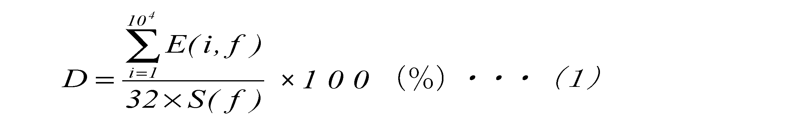
上記式(1)中の値E(i,f)は、動作周波数fにおけるi番目の入力データXについて、演算結果データV1、V2の間で不一致となるビット数である。また、S(f)は、動作周波数fにおけるエラー検知回数である。
The value E (i, f) in the above equation (1) is the number of bits that do not match between the operation result data V1 and V2 for the i-th input data X at the operating frequency f. S (f) is the number of times of error detection at the operating frequency f.
さらに、この検証試験では、検証例と比較するために、DSPブロック12が最大限使用された演算回路L1を2個形成したFPGAについてのタイミングシミュレーションを比較例1とし、さらに、DSPブロック12以外の回路ブロックを組み合わせた演算回路L2を2個形成したFPGAについてのタイミングシミュレーションを比較例2とした。これら比較例1および比較例2のFPGAにそれぞれ演算回路L1、L2を形成する各構成情報は、検証例と同様にしてそれぞれ生成した。そして、比較例1及び比較例2についても、検証例と同様にシミュレーションツール上にてタイミングシミュレーションを行った。それら比較例1及び比較例2の検証結果についても図4~図6に併せて示す。
Further, in this verification test, for comparison with the verification example, a timing simulation for an FPGA in which two arithmetic circuits L1 in which the DSP block 12 is used to the maximum is formed is referred to as Comparative Example 1. A timing simulation of an FPGA in which two arithmetic circuits L2 formed by combining circuit blocks are formed is referred to as Comparative Example 2. The configuration information for forming the arithmetic circuits L1 and L2 in the FPGAs of Comparative Example 1 and Comparative Example 2 was generated in the same manner as in the verification example. And also about the comparative example 1 and the comparative example 2, the timing simulation was performed on the simulation tool similarly to the verification example. The verification results of Comparative Example 1 and Comparative Example 2 are also shown in FIGS.
図4に示すように、DSPブロック12を使用した演算回路L1を2個形成した比較例1では、176MHzよりも上の動作周波数で、エラー発生率がほぼ100%になった。DSPブロック12を使用しない演算回路L2を2個形成した比較例2では、動作周波数が204MHzからエラーが発生し、動作周波数の上昇とともにエラーの発生率が100%に近づくように上昇した。このことから、エラーの発生状況は回路ブロックの組み合わせによって互いに異なることがわかる。なお、本発明を適用した検証例では、178MHzよりも上の動作周波数でエラー発生率がほぼ100%となり、比較例1と同様なエラーの発生状況となった。
As shown in FIG. 4, in Comparative Example 1 in which two arithmetic circuits L1 using the DSP block 12 were formed, the error rate was almost 100% at an operating frequency higher than 176 MHz. In Comparative Example 2 in which two arithmetic circuits L2 that do not use the DSP block 12 were formed, an error occurred from an operating frequency of 204 MHz, and the error rate increased so as to approach 100% as the operating frequency increased. From this, it can be seen that error occurrence states differ depending on the combination of circuit blocks. In the verification example to which the present invention was applied, the error occurrence rate was almost 100% at an operating frequency higher than 178 MHz, and the same error occurrence situation as in Comparative Example 1 was obtained.
上記から比較例1では、178MHz以上の動作周波数のとき、2個の演算回路L1のうち少なくとも一方から出力された演算結果データが誤った値となっていることが分かる。しかしながら、図5に示されるように、比較例1では、178MHz以上のいくつかの動作周波数でエラーを検知しているが、その他の動作周波数ではエラーを検知していない。この理由として、比較例1では、同じ回路ブロックの組み合わせでなる2個の演算回路L1を用いていることから、2個の演算回路L1でそれぞれ同じエラーが発生してしまい、それぞれ出力される演算結果データが全く同じとなり、その結果、エラーとして検知できないためである。比較例2では、エラー検知率がほぼ100%であるが、218MHzよりも上の動作周波数では、1~2%程度のエラー検知率の低下が見られた。
From the above, in Comparative Example 1, it can be seen that the operation result data output from at least one of the two operation circuits L1 has an incorrect value at an operating frequency of 178 MHz or higher. However, as shown in FIG. 5, in Comparative Example 1, errors are detected at several operating frequencies of 178 MHz or higher, but errors are not detected at other operating frequencies. This is because, in Comparative Example 1, two arithmetic circuits L1 composed of the same circuit block combination are used, so that the same error occurs in each of the two arithmetic circuits L1, and the respective arithmetic operations to be output This is because the result data is exactly the same and as a result cannot be detected as an error. In Comparative Example 2, the error detection rate is almost 100%, but at the operating frequency above 218 MHz, a decrease in the error detection rate of about 1 to 2% was observed.
これらに対して本発明による検証例のエラー検知率は、すべての動作周波数において100%となった。すなわち、比較例1及び比較例2のように回路ブロックの組み合わせが同じ複数の演算回路が冗長化した構成よりも、本発明の検証例のように、回路ブロックの組み合わせが異なる複数の演算回路L1、L2、すなわち多様性を持った複数の演算回路を形成した構成とすることにより、一段と確実にエラーを検知でき、かくして、エラーの検知率が向上することが確認できた。また、図6に示すように、検証例における不一致距離は、比較例1及び比較例2よりも3倍以上大きいことが確認できた。すなわち、比較例1及び比較例2のように同じ回路構成を有する複数の演算回路によって冗長化した構成を形成するよりも、本発明の検証例のように、互いに回路ブロックの組み合わせが異なる多様性を持った複数の演算回路を形成するほうが、エラーの検知能力が高いことが示された。
In contrast, the error detection rate of the verification example according to the present invention was 100% at all operating frequencies. That is, rather than a configuration in which a plurality of arithmetic circuits having the same combination of circuit blocks are made redundant as in Comparative Example 1 and Comparative Example 2, a plurality of arithmetic circuits L1 having different combinations of circuit blocks as in the verification example of the present invention. L2, that is, by using a configuration in which a plurality of arithmetic circuits having diversity are formed, it has been confirmed that errors can be detected more reliably, thus improving the error detection rate. Further, as shown in FIG. 6, it was confirmed that the mismatch distance in the verification example was three times or more larger than that in Comparative Example 1 and Comparative Example 2. In other words, rather than forming a redundant configuration with a plurality of arithmetic circuits having the same circuit configuration as in Comparative Example 1 and Comparative Example 2, the diversity of combinations of circuit blocks differing from each other as in the verification example of the present invention. It was shown that the error detection capability is higher when a plurality of arithmetic circuits having the above are formed.
10 FPGA(プログラマブルロジックデバイス)
11 基本論理ブロック
12 DSPブロック
21 検証回路
L1~L3 演算回路 10 FPGA (Programmable Logic Device)
11basic logic block 12 DSP block 21 verification circuit L1 to L3 arithmetic circuit
11 基本論理ブロック
12 DSPブロック
21 検証回路
L1~L3 演算回路 10 FPGA (Programmable Logic Device)
11
Claims (6)
- 複数の回路ブロックの組み合わせを変えることにより、演算機能が変更可能なプログラマブルロジックデバイスにおいて、
前記回路ブロックの組み合わせ及び接続状態が互いに異なり、かつ互いに同じ演算をする第1演算回路及び第2演算回路と、
前記第1演算回路及び前記第2演算回路のそれぞれに設けられており、演算結果を検証する検証回路に前記第1演算回路及び前記第2演算回路の演算結果を出力する出力部と、
を備えることを特徴とするプログラマブルロジックデバイス。 In programmable logic devices that can change the calculation function by changing the combination of multiple circuit blocks,
A first arithmetic circuit and a second arithmetic circuit in which the combination and connection state of the circuit blocks are different from each other and perform the same operation;
An output unit that is provided in each of the first arithmetic circuit and the second arithmetic circuit, and outputs an arithmetic result of the first arithmetic circuit and the second arithmetic circuit to a verification circuit that verifies the arithmetic result;
A programmable logic device comprising: - 前記第1演算回路は、前記回路ブロックの1つであるDSPブロックを含み、
前記第2演算回路は、前記DSPブロック以外の前記回路ブロックで構成される
ことを特徴とする請求項1に記載のプログラマブルロジックデバイス。 The first arithmetic circuit includes a DSP block which is one of the circuit blocks,
The programmable logic device according to claim 1, wherein the second arithmetic circuit includes the circuit blocks other than the DSP block. - 前記回路ブロックの組み合わせにより形成された前記検証回路を備えることを特徴とする請求項1または2に記載のプログラマブルロジックデバイス。 The programmable logic device according to claim 1 or 2, further comprising the verification circuit formed by a combination of the circuit blocks.
- 複数の回路ブロックの組み合わせを変えることにより、演算機能が変更可能なプログラマブルロジックデバイスのエラー検証方法において、
前記回路ブロックの組み合わせ及び接続状態が互いに異なり、かつ互いに同じ演算をする第1演算回路及び第2演算回路を形成する回路形成ステップと、
前記第1演算回路及び前記第2演算回路でそれぞれ演算を行う演算ステップと、
前記第1演算回路及び前記第2演算回路からの演算結果を検証する検証ステップと
を有することを特徴とするプログラマブルロジックデバイスのエラー検証方法。 In an error verification method for a programmable logic device in which an arithmetic function can be changed by changing a combination of a plurality of circuit blocks,
A circuit forming step for forming a first arithmetic circuit and a second arithmetic circuit in which the combination and connection state of the circuit blocks are different from each other and perform the same operation;
A calculation step of performing calculation in each of the first calculation circuit and the second calculation circuit;
An error verification method for a programmable logic device, comprising: a verification step for verifying a calculation result from the first calculation circuit and the second calculation circuit. - 前記回路形成ステップは、
前記第1演算回路を、前記回路ブロックの1つであるDSPブロックを含む構成とし、
前記第2演算回路を、前記DSPブロック以外の前記回路ブロックで構成する
ことを特徴とする請求項4に記載のプログラマブルロジックデバイスのエラー検証方法。 The circuit forming step includes
The first arithmetic circuit includes a DSP block that is one of the circuit blocks,
The error verification method for a programmable logic device according to claim 4, wherein the second arithmetic circuit is configured by the circuit block other than the DSP block. - 構成情報にしたがって複数の回路ブロックの組み合わせを変えることにより、演算機能が変更可能なプログラマブルロジックデバイスの回路形成方法において、
前記回路ブロックの組み合わせに関する条件が異なる合成パラメータを順次設定する合成パラメータ設定ステップと、
前記合成パラメータ設定ステップで前記合成パラメータが設定されるごとに、設定された前記合成パラメータの下で論理合成を行い、ハードウェア記述言語で記述された同一の演算回路記述情報から複数の演算回路に対応した複数のネットリストを生成する論理合成ステップと、
前記複数のネットリストから前記構成情報を生成する構成情報生成ステップと、
前記構成情報をプログラマブルロジックデバイスに書き込み、前記複数のネットリストに対応して、前記回路ブロックの組み合わせ及び接続状態が互いに異なり、かつ互いに同じ演算をする第1演算回路及び第2演算回路と、前記第1演算回路及び前記第2演算回路にそれぞれ設けられ、演算結果を検証する検証回路に前記第1演算回路及び前記第2演算回路の演算結果を出力する出力部とを前記プログラマブルロジックデバイスに形成する形成ステップと
を有することを特徴とするプログラマブルロジックデバイスの回路形成方法。 In a circuit formation method of a programmable logic device in which an arithmetic function can be changed by changing a combination of a plurality of circuit blocks according to configuration information,
A synthesis parameter setting step for sequentially setting synthesis parameters having different conditions regarding the combination of the circuit blocks;
Each time the synthesis parameter is set in the synthesis parameter setting step, logic synthesis is performed under the set synthesis parameter, and the same arithmetic circuit description information described in a hardware description language is used to generate a plurality of arithmetic circuits. A logic synthesis step for generating a plurality of corresponding netlists;
A configuration information generating step for generating the configuration information from the plurality of netlists;
Writing the configuration information into a programmable logic device, corresponding to the plurality of netlists, a combination of the circuit blocks and a connection state are different from each other, and a first arithmetic circuit and a second arithmetic circuit that perform the same arithmetic operation; Provided in each of the first arithmetic circuit and the second arithmetic circuit, and in the programmable logic device, an output unit for outputting the arithmetic result of the first arithmetic circuit and the second arithmetic circuit is formed in a verification circuit for verifying the arithmetic result A circuit forming method for a programmable logic device, comprising: a forming step.
Priority Applications (2)
| Application Number | Priority Date | Filing Date | Title |
|---|---|---|---|
| US15/572,140 US10067742B2 (en) | 2015-05-07 | 2016-02-24 | Programmable logic device, method for verifying error of programmable logic device, and method for forming circuit of programmable logic device |
| EP16789468.2A EP3293883B1 (en) | 2015-05-07 | 2016-02-24 | Programmable logic device, method for verifying error of programmable logic device, and method for forming circuit of programmable logic device |
Applications Claiming Priority (2)
| Application Number | Priority Date | Filing Date | Title |
|---|---|---|---|
| JP2015094970A JP5807887B1 (en) | 2015-05-07 | 2015-05-07 | Programmable logic device, programmable logic device error verification method, and programmable logic device circuit formation method |
| JP2015-094970 | 2015-05-07 |
Publications (1)
| Publication Number | Publication Date |
|---|---|
| WO2016178332A1 true WO2016178332A1 (en) | 2016-11-10 |
Family
ID=54545798
Family Applications (1)
| Application Number | Title | Priority Date | Filing Date |
|---|---|---|---|
| PCT/JP2016/055389 WO2016178332A1 (en) | 2015-05-07 | 2016-02-24 | Programmable logic device, method for verifying error of programmable logic device, and method for forming circuit of programmable logic device |
Country Status (4)
| Country | Link |
|---|---|
| US (1) | US10067742B2 (en) |
| EP (1) | EP3293883B1 (en) |
| JP (1) | JP5807887B1 (en) |
| WO (1) | WO2016178332A1 (en) |
Families Citing this family (2)
| Publication number | Priority date | Publication date | Assignee | Title |
|---|---|---|---|---|
| JP6696352B2 (en) * | 2016-08-18 | 2020-05-20 | 富士通株式会社 | Programmable logic device, information processing device, processing method, and processing program |
| CN110096397B (en) * | 2019-03-27 | 2022-10-25 | 天津大学 | Multi-ring oscillator FPGA configuration circuit robustness detection method |
Citations (2)
| Publication number | Priority date | Publication date | Assignee | Title |
|---|---|---|---|---|
| JP2001099627A (en) * | 1999-07-23 | 2001-04-13 | Matsushita Electric Works Ltd | Image processing system and its constituting method |
| JP2011216020A (en) * | 2010-04-01 | 2011-10-27 | Mitsubishi Electric Corp | Information processing apparatus and circuit reconfiguration device |
Family Cites Families (8)
| Publication number | Priority date | Publication date | Assignee | Title |
|---|---|---|---|---|
| JP5310036B2 (en) * | 2009-01-30 | 2013-10-09 | 富士通株式会社 | Verification support program and verification support apparatus |
| JP5532048B2 (en) * | 2009-07-13 | 2014-06-25 | 日本電気株式会社 | Anonymous authentication signature system, user device, verification device, signature method, verification method and program thereof |
| NL1037275C2 (en) * | 2009-09-11 | 2011-03-14 | Advanced Public Transp Systems B V | DRIVING DEVICE FOR A PRE-DEFINED TRAVEL MOBILE VEHICLE, AUTOMATICALLY DRIVEN AND THROUGH AT LEAST A FIRST AXLE, AND A VEHICLE EQUIPPED WITH SUCH STEERING DEVICE. |
| US8365131B2 (en) * | 2010-01-11 | 2013-01-29 | Empire Technology Development Llc | Hardware synthesis using thermally aware scheduling and binding |
| JP2012043197A (en) * | 2010-08-19 | 2012-03-01 | Toshiba Tec Corp | Information processor and program |
| US20140237263A1 (en) * | 2013-02-19 | 2014-08-21 | Kabushiki Kaisha Toshiba | Nonvolatile semiconductor memory device and memory system using the same |
| US8769450B1 (en) * | 2013-06-28 | 2014-07-01 | Xilinx, Inc. | Synthesis flow for formal verification |
| JP6528612B2 (en) * | 2015-08-31 | 2019-06-12 | 株式会社ソシオネクスト | POWER SUPPLY VOLTAGE CONTROL CIRCUIT, POWER SUPPLY VOLTAGE CONTROL METHOD, AND POWER SUPPLY VOLTAGE CONTROL PROGRAM |
-
2015
- 2015-05-07 JP JP2015094970A patent/JP5807887B1/en active Active
-
2016
- 2016-02-24 EP EP16789468.2A patent/EP3293883B1/en active Active
- 2016-02-24 US US15/572,140 patent/US10067742B2/en active Active
- 2016-02-24 WO PCT/JP2016/055389 patent/WO2016178332A1/en active Application Filing
Patent Citations (2)
| Publication number | Priority date | Publication date | Assignee | Title |
|---|---|---|---|---|
| JP2001099627A (en) * | 1999-07-23 | 2001-04-13 | Matsushita Electric Works Ltd | Image processing system and its constituting method |
| JP2011216020A (en) * | 2010-04-01 | 2011-10-27 | Mitsubishi Electric Corp | Information processing apparatus and circuit reconfiguration device |
Non-Patent Citations (1)
| Title |
|---|
| See also references of EP3293883A4 * |
Also Published As
| Publication number | Publication date |
|---|---|
| EP3293883A1 (en) | 2018-03-14 |
| EP3293883A4 (en) | 2018-12-19 |
| US20180129471A1 (en) | 2018-05-10 |
| JP2016213637A (en) | 2016-12-15 |
| EP3293883B1 (en) | 2020-11-18 |
| JP5807887B1 (en) | 2015-11-10 |
| US10067742B2 (en) | 2018-09-04 |
Similar Documents
| Publication | Publication Date | Title |
|---|---|---|
| US10289483B2 (en) | Methods and apparatus for embedding an error correction code in storage circuits | |
| US8997033B1 (en) | Techniques for generating a single configuration file for multiple partial reconfiguration regions | |
| JP6363297B2 (en) | Simulator, design support system and method for semiconductor circuit device | |
| EP3324317B1 (en) | Methods for verifying retimed circuits with delayed initialization | |
| Moreira et al. | Impact of C-elements in asynchronous circuits | |
| US20100313176A1 (en) | Delay library, delay library creation method, and delay calculation method | |
| US8977998B1 (en) | Timing analysis with end-of-life pessimism removal | |
| US20170328951A1 (en) | Embedded built-in self-test (bist) circuitry for digital signal processor (dsp) validation | |
| US11748548B2 (en) | Hierarchical clock tree implementation | |
| CN102460582B (en) | Embedded digital ip strip chip | |
| WO2016178332A1 (en) | Programmable logic device, method for verifying error of programmable logic device, and method for forming circuit of programmable logic device | |
| US10162916B1 (en) | Timing verification in a programmable circuit design using variation factors | |
| US7603646B1 (en) | Method and apparatus for power optimization using don't care conditions of configuration bits in lookup tables | |
| US8813018B1 (en) | Method and apparatus for automatically configuring memory size | |
| US8893068B1 (en) | Techniques to generate a more accurate simulation model | |
| KR20180051708A (en) | Layout method for semiconductor device based on swiching activity and manufacturing | |
| US10302698B1 (en) | Estimation of power consumed by combinatorial circuitry | |
| US9152756B2 (en) | Group based routing in programmable logic device | |
| US8881082B2 (en) | FEC decoder dynamic power optimization | |
| US9672307B2 (en) | Clock placement for programmable logic devices | |
| JP7051151B2 (en) | Numerical information generator, numerical information generation method and program | |
| US9268891B1 (en) | Compact and efficient circuit implementation of dynamic ranges in hardware description languages | |
| US10565334B1 (en) | Targeted delay optimization through programmable clock delays | |
| US7681160B1 (en) | Weight based look up table collapsing for programmable logic devices | |
| US9053271B1 (en) | Integrated circuit reset system modification tool |
Legal Events
| Date | Code | Title | Description |
|---|---|---|---|
| 121 | Ep: the epo has been informed by wipo that ep was designated in this application |
Ref document number: 16789468 Country of ref document: EP Kind code of ref document: A1 |
|
| WWE | Wipo information: entry into national phase |
Ref document number: 15572140 Country of ref document: US |
|
| NENP | Non-entry into the national phase |
Ref country code: DE |