WO2016175262A1 - 光学フィルタ部材を生産する方法、光学フィルタ部材及び光測定装置 - Google Patents
光学フィルタ部材を生産する方法、光学フィルタ部材及び光測定装置 Download PDFInfo
- Publication number
- WO2016175262A1 WO2016175262A1 PCT/JP2016/063278 JP2016063278W WO2016175262A1 WO 2016175262 A1 WO2016175262 A1 WO 2016175262A1 JP 2016063278 W JP2016063278 W JP 2016063278W WO 2016175262 A1 WO2016175262 A1 WO 2016175262A1
- Authority
- WO
- WIPO (PCT)
- Prior art keywords
- dye
- optical filter
- filter member
- silicone resin
- light
- Prior art date
- Legal status (The legal status is an assumption and is not a legal conclusion. Google has not performed a legal analysis and makes no representation as to the accuracy of the status listed.)
- Ceased
Links
Images






Classifications
-
- G—PHYSICS
- G01—MEASURING; TESTING
- G01N—INVESTIGATING OR ANALYSING MATERIALS BY DETERMINING THEIR CHEMICAL OR PHYSICAL PROPERTIES
- G01N21/00—Investigating or analysing materials by the use of optical means, i.e. using sub-millimetre waves, infrared, visible or ultraviolet light
- G01N21/62—Systems in which the material investigated is excited whereby it emits light or causes a change in wavelength of the incident light
- G01N21/63—Systems in which the material investigated is excited whereby it emits light or causes a change in wavelength of the incident light optically excited
- G01N21/64—Fluorescence; Phosphorescence
-
- G—PHYSICS
- G02—OPTICS
- G02B—OPTICAL ELEMENTS, SYSTEMS OR APPARATUS
- G02B5/00—Optical elements other than lenses
- G02B5/20—Filters
- G02B5/22—Absorbing filters
Definitions
- the present invention relates to a method for producing an optical filter member, an optical filter member, and an optical measurement device.
- the inventors previously proposed a light-induced fluorescence measurement device that can meet the demand for point-of-care testing (POCT) in the life science field.
- This measuring apparatus is a small and portable device that has a short inspection time and high-precision evaluation analysis in the field where analysis is required.
- a measuring method for example, laser induced fluorescence (Laser Induced Fluorescence: LIF) is used.
- LIF is caused by exciting a measurement target (atom or molecule) by irradiating a laser beam that matches the excitation level (tuned wavelength) using the resonance transition of the target atom or molecule.
- This is a technique for measuring emitted luminescence (fluorescence).
- the concentration of the measurement object is calculated from the intensity of the fluorescence, and the temperature of the measurement object is calculated from the spectrum distribution of the fluorescence.
- the inventors replaced the colored glass filter that absorbs light other than the fluorescence emitted from the sample with an organic optical functional material (resin or the like) having optical performance equivalent to that of the colored glass filter. It was proposed to use an optical material in which an organic optical functional material is dispersed in a polymer substance.
- Patent Document 1 proposes a solid dye laser medium in which polydimethylsiloxane (hereinafter also referred to as PDMS) contains, for example, a pyromethene dye.
- PDMS polydimethylsiloxane
- Patent Document 2 in a microfluidic device in which an excitation light source and a detector are provided on a microchip having a flow path (microchannel) through which a sample is injected and discharged, an optical that selectively transmits only a necessary wavelength.
- an organic light functional material in which a pigment belonging to, for example, the Sudan dye family is dispersed in PDMS is used.
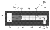
- FIG. 12 shows a configuration example of the light-induced fluorescence measuring apparatus 101 proposed by the inventors (see Patent Document 3). Note that the photoinduced fluorescence measurement apparatus 101 shown in FIG. 12 is not known at the time of filing this application.
- the light-induced fluorescence measurement apparatus 101 includes a solid-state light source 103 such as a laser light source, a sample holding unit 105 that holds a sample to be measured, a fluorescence collection optical system including a lens and an optical filter, and a fluorescence measuring instrument 109 such as a photomultiplier tube. Including.
- the light emitting surface 107 of the laser light source (solid light source 103) and the light receiving surface 111 of the photomultiplier tube (fluorescence measuring instrument 109) emit excitation light from the solid light source 103 and fluorescence emitted from the sample. It is embedded in or is in contact with a resin such as PDMS that is transparent to the light it contains. Further, the fluorescence collecting optical system formed in the optical path from the light emitting surface 107 to the light receiving surface 111 is also embedded in a transparent resin such as PDMS, and the transparent resin itself constitutes the fluorescence collecting optical system. That is, the light emitting surface 107 of the laser light source, the sample holder 105, the fluorescence collecting optical system, and the light receiving surface 111 of the photomultiplier tube are integrally held and positioned by a transparent resin.
- the fluorescence collecting optical system includes a first silicone resin 165, a first air chamber 167, a second silicone resin 169, a notch filter 171, a third silicone resin 173, a second air chamber 175, and an optical filter 151 (structure). 1).
- the optical filter 151 removes light other than fluorescence, which is a measurement target, from autofluorescent stray light and Raman light, and includes a dye diffusion suppression member 177 and a dye-containing silicone resin 179.
- the transparent resin structure that holds each component integrally is generated from the resin when the excitation light, autofluorescence generated when the sample case is irradiated with the excitation light, and excitation light travel through the resin. It is surrounded by a resin containing a pigment having wavelength characteristics that absorbs Raman light substantially uniformly. That is, the resin containing the pigment constitutes a housing 113 that holds the sample holder 105, the fluorescence measuring instrument 109, the fluorescence collection optical system, and the like.
- the solid light source 103 and the fluorescence measuring device 109 are embedded as necessary, and power is supplied to the solid light source 103 and the fluorescence measuring device 109 which are not shown. Power source to be buried. For this reason, the position of the optical element or the like hardly changes and is stable against an external impact, and a holder for holding the optical element is not required. Therefore, the light-induced fluorescence measuring apparatus 101 is small and portable.
- the silicone resin that surrounds the light guide space through which light passes is generated from the resin when the excitation light, autofluorescence generated when the sample case is irradiated with excitation light, and excitation light travels through the resin. Because it contains a pigment with wavelength characteristics that absorbs Raman light almost uniformly, the excitation light and measurement light fluorescence are not emitted to the outside of the device, and light from the outside is inside the fluorescence collection optical system etc. There is no entry. Therefore, highly accurate measurement is possible. Further, stray light such as excitation light and its reflected / scattered light is once absorbed into the pigment-containing resin, and the complex multiple reflection of stray light hardly occurs. Therefore, the fluorescence collecting optical system does not need to cope with the complex reflection of stray light and is simplified, and as a result, the light-induced fluorescence measuring apparatus 101 is downsized.
- An object of the present invention is to provide an optical filter that prevents stray light from propagating through a dye diffusion suppressing portion while preventing the dye from flowing out from the dye-containing silicone resin to the outside (black pigment-containing silicone resin).
- a first aspect of the present invention is a method for producing an optical filter member, wherein an excitation light or an exciter that excites oxygen molecules is applied to a silicone resin, whereby the dye is dispersed from the silicone resin to which the dye is dispersed. It is the method of producing an optical filter member including the excitation step which forms the pigment
- a second aspect of the present invention is a method for producing the optical filter member according to the first aspect, further comprising a dye dispersion step of dispersing the dye in the silicone resin before the excitation step.
- a method for producing a member is a method for producing the optical filter member according to the first aspect, further comprising a dye dispersion step of dispersing the dye in the silicone resin before the excitation step.
- a third aspect of the present invention is a method for producing the optical filter member according to the first aspect, wherein the dye diffusion suppression part is formed around a dye dispersion part that is a silicone resin in which the dye is dispersed, Or it is the method of producing the optical filter member which forms the said pigment dispersion part in the space which the said pigment
- a fourth aspect of the present invention is a method for producing an optical filter member according to any one of the first to third aspects, wherein, in the excitation step, vacuum ultraviolet light is applied to the silicone resin as the excitation light. This is a method for producing an optical filter member.
- a method for producing an optical filter member according to the fourth aspect wherein in the excitation step, the optical filter member is irradiated with at least 1.8 J / cm 2 of the vacuum ultraviolet light. Is the method.
- a method for producing an optical filter member according to any one of the first to third aspects, wherein, in the excitation step, the silicone resin is plasma with atmospheric pressure plasma as the exciter.
- This is a method for producing an optical filter member by applying a process gas.
- a method for producing an optical filter member according to the sixth aspect wherein an optical filter member is applied in which at least 146 J / cm 2 of the plasma process gas is applied in the excitation step. Is the method.
- An eighth aspect of the present invention is an optical filter member, which is a dye diffusion that suppresses diffusion of the dye from the dye dispersion part to the outside around the dye dispersion part in which the dye is dispersed inside the silicone resin. It is an optical filter member provided with the suppression part, and in the said pigment
- a ninth aspect of the present invention is the optical filter member according to the eighth aspect, wherein in the dye diffusion suppression unit, there are three or more silicon atoms at a depth of 1 ⁇ m from the surface of the dye diffusion suppression unit.
- the ratio of bonding to oxygen atoms is an optical filter member that is higher than the ratio of bonding a plurality of silicon atoms at a depth of 2 ⁇ m from the surface to three or more oxygen atoms.
- a tenth aspect of the present invention is the optical filter member according to the ninth aspect, wherein in the dye diffusion suppression unit, the closer to the surface, the higher the proportion of silicon atoms bonded to three or more oxygen atoms.
- the optical filter member in the dye diffusion suppression unit, the closer to the surface, the higher the proportion of silicon atoms bonded to three or more oxygen atoms.
- An eleventh aspect of the present invention is an optical measurement device including the optical filter member according to any one of the eighth to tenth aspects.
- the ratio of silicon atoms bonded to three or more oxygen atoms inside the dye diffusion suppressing portion continuously changes. Therefore, it is possible to form a dye diffusion suppression portion whose refractive index continuously changes.
- the dye diffusion suppression unit has a weak light confinement function and becomes a light guide with a large loss. As a result, it is possible to suppress the propagation of stray light through the dye diffusion suppression unit while preventing the dye from flowing out from the dye-containing silicone resin to the outside (black pigment-containing silicone resin).
- the reflection of light on both surfaces of the dye diffusion suppression member 201 interferes, and thus shows wavelength-dependent reflection characteristics.
- a clear boundary between the portion having a quartz glass (SiO 2 ) -like bond and the silicone resin is one of the surfaces of the pigment dispersion portion (the surface of the pigment diffusion suppression portion). Only exists. Therefore, interference between the two surfaces does not occur, and scattering of a specific wavelength due to the etalon effect or the like can be suppressed.
- an optical filter member can be produced based on a plurality of specific manufacturing processes.
- At least a part of silicon atoms are bonded to two oxygen atoms in the dye diffusion suppressing part having a thickness of at least 2 ⁇ m or more from the surface of the dye dispersing part. Since the dye diffusion suppressing member does not allow the dye to pass therethrough, it is possible to produce an optical filter member including a dye diffusion suppressing unit having an appropriate thickness.
- FIG. 3 is a graph showing the degree of pigment dispersion in Example 1.
- FIG. 6 is a cross-sectional view of an example of a pressure plasma apparatus in Embodiment 2.
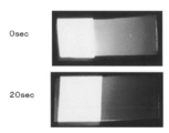
- FIG. It is a figure which shows the change by the irradiation time of the contact angle of water on the resin surface. It is a figure which shows the dispersion
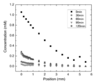
- FIG. 6 is a graph showing the degree of dispersion of a dye in Example 2.
- 1 is an overall view of a conventional light-induced fluorescence measuring apparatus previously proposed by the inventors of the present invention.
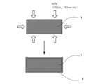
- FIG. 1 shows an example of a method for producing an optical filter member according to the present invention (an example of “an optical filter member” in the claims of the present application) (an example of an “method of producing an optical filter member” in the claims of the present application).
- a cured transparent silicone resin (an example of “silicone resin” in the claims) is immersed in a dye solution such as Sudan (an example of “dye” in the claims). Disperse the dye inside the silicone resin.
- a liquid silicone resin in which a pigment is dispersed may be cured.
- the dye-containing silicone resin 1 (an example of the “dye dispersion part” in the claims) is produced (an example of the “dye dispersion step” in the claims).
- VUV vacuum ultraviolet light having a wavelength of 200 nm or less as excitation light for exciting oxygen molecules on the surface of the dye-containing silicone resin 1
- excitation step an example of “excitation step” in claims of this application.
- the phrase “irradiate” in the present embodiment is an example of “apply” in the claims of the present application.
- the VUV is, for example, light having a wavelength of 172 nm emitted from a Xe excimer lamp or light having a wavelength of 157 nm emitted from an F 2 excimer laser device.
- oxygen existing near the surface of the dye-containing silicone resin 1 is considered to be an oxygen atom in an excited state by the following mechanism.
- oxygen molecules in the air absorb ultraviolet rays to be in an excited state (Equation 1), and next, excited oxygen molecules become excited oxygen atoms (Equation 2).
- oxygen molecules in the air absorb ultraviolet rays and become two excited oxygen atoms (Formula 3).
- PDMS silicon atoms are bonded to two methyl groups on the resin surface 5 (an example of “surface” in the claims).
- the resin surface 5 is irradiated with VUV, the methyl group bonded to the silicon atom is released and bonded to the excited oxygen atom generated by the above mechanism.
- the methyl group of the siloxane structure is substituted with an oxygen atom, and the dye diffusion suppression unit 3 having a silicon dioxide (SiO 2 ) -like bond on the resin surface 5 is generated.
- the dye diffusion suppression unit 3 at least some of the plurality of silicon atoms are bonded to three or four oxygen atoms.
- the substitution rate to the quartz glass (SiO 2 ) -like bond formed on the surface of the dye-containing silicone resin 1 gradually decreases as the depth increases from the surface to the inside.
- a structure in which the refractive index is continuously changed is manufactured.
- the PDMS internal absorption of light having a wavelength of 172 nm is about 2.4 ⁇ m, and that it is replaced with SiO 2 at a depth of about 2 ⁇ m.
- the refractive index changes exponentially from 1.45 to 1.41 in the depth direction from the surface to the inside.
- the clear boundary surface between the portion having a quartz glass (SiO 2 ) -like bond and the silicone resin is an asymmetric waveguide limited to one layer.
- the dye diffusion suppression unit 3 is a waveguide having a weak light confinement function and a large loss. Accordingly, it is possible to effectively suppress the light from being guided and detoured as compared with the conventional dye diffusion suppressing member having a thick film structure.
- the tolerance for bending that the waveguide can propagate is as large as about 10 mm in radius of curvature. Therefore, when the dye diffusion suppression unit 3 is used as a resin shell surrounding the optical element, light does not propagate even with a slight bend. That is, it is easy to suppress detouring of light.
- the number of reflections at the interface per unit length of the optical waveguide is inversely proportional to the film thickness.
- the thickness of the conventional dye diffusion suppressing member is 0.5 mm and the thickness of the dye diffusion suppressing portion 3 of this embodiment is 2 ⁇ m
- the intensity of the propagating light is attenuated to 1/250. In this embodiment, even if the loss per reflection at the boundary is slightly increased, it is easy to lose the function as a substantial waveguide.
- the dye dispersed in the dye-containing silicone resin 1 is blocked by the dye diffusion suppression unit 3 according to this embodiment (black) and does not move to the pigment-containing silicone resin. Therefore, the optical performance equivalent to the colored glass filter included in the optical filter according to the present embodiment does not deteriorate. Therefore, it becomes easy to maintain the measurement accuracy of the measurement target light (an example of “measurement target light” in the claims) by the optical measurement device.
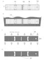
- FIGS. 3 and 4 an example of a method for manufacturing the light measurement device 31 of the present invention (an example of “light measurement device” in the claims of the present application) will be described with reference to FIGS. 3 and 4.
- a structure in which a first air chamber 9, a second air chamber 11, a sample case holder 13 and a notch filter 15 are embedded in a transparent silicone resin (PDMS) 7 is manufactured (FIG. 3).
- PDMS transparent silicone resin
- FIG. 3C is irradiated with VUV to form the dye diffusion suppression portion 21 on the surface of the dye-containing silicone resin 19 (FIG. 3D); An example of “step”). Further, the photomultiplier tube 23 and the DPSS laser 25 are arranged at predetermined positions in the optical system in which the dye diffusion suppression portion 21 on the surface of the dye-containing silicone resin 19 shown in FIG. e)). Subsequently, a set of optical systems shown in FIG. 4E is placed in the mold 27, and a liquid black pigment-containing silicone resin 29 is poured and cured (FIG. 4F). Finally, the mold member 27 is removed, and the light measuring device 31 is completed as shown in FIG.
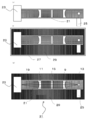
- FIG. 5 is a diagram showing an outline of an experiment for examining the relationship between the degree of dispersion of the dye in PDMS and the light irradiation treatment conditions.
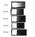
- FIG. 6 is a diagram showing the result of dispersing the dye in PDMS when the irradiation conditions are changed.
- FIG. 7 is a graph showing the degree of pigment dispersion.
- a dye-dispersed PDMS 51 in which a dye P597 (pyromethene 597) is dispersed in PDMS (SIM-360: manufactured by Shin-Etsu Silicone (registered trademark)) is used.
- the degree of dispersion of the dye from the dye-dispersed PDMS 51 to the dye-undispersed PDMS 53 was observed by contacting with the dispersed PDMS 53.
- the dye-dispersed PDMS 51 has a cubic shape with a side of 3 mm.
- the pigment non-dispersed PDMS 53 has a rectangular parallelepiped shape with a height of 1 mm, a depth of 4 mm, and a width of 5 mm or more. Further, of 6 surfaces of the pigment-undispersed PDMS 53, the contact surface 55 with the pigment-dispersed PDMS 51 is irradiated with 10 mW / cm 2 of vacuum ultraviolet light for 30, 60, 90, 120 minutes to perform vitrification treatment. Compared with the degree of dispersion when not.
- FIG. 6 shows the observation results of the degree of dispersion of the pigment in the pigment-undispersed PDMS 53 after the pigment-dispersed PDMS 51 is brought into contact with the contact surface 55 subjected to the vitrification treatment of the pigment-undispersed PDMS 53 and allowed to stand for 72 hours.
- the vacuum ultraviolet light was not irradiated at all, the dye was easily dispersed inside the dye-undispersed PDMS 53.
- the vacuum ultraviolet light was irradiated for 30 minutes or more, the pigment dispersion inside the pigment non-dispersed PDMS 53 was clearly suppressed.
- the graph shown in FIG. 7 also shows that the concentration of the dye dispersed in the dye-undispersed PDMS 53 was suppressed by irradiation with vacuum ultraviolet light.
- the light applied to the surface of the pigment dispersion portion may be light other than vacuum ultraviolet light as long as it is excitation light that excites oxygen molecules.
- Example 1 the surface of the dye-containing silicone resin 1 is irradiated with VUV to excite oxygen present in the vicinity of the surface of the dye-containing silicone resin 1 to generate excited oxygen atoms. It was.
- Example 2 instead of irradiating the surface of the dye-containing silicone resin 1 with VUV, atmospheric pressure plasma particles (processed as “excited substance” and “plasmaized” in the claims of the present application), which is a process gas converted into plasma with atmospheric pressure plasma, are used.
- An example of “process gas” is irradiated on the surface of the dye-containing silicone resin 1 (an example of “excitation step” in the claims of the present application).
- the phrase “irradiate” in the present embodiment is an example of “apply” in the claims of the present application.
- FIG. 8 is a cross-sectional view of an example of the atmospheric pressure plasma apparatus 59 used in the second embodiment.
- the atmospheric pressure plasma device 59 includes a rectangular parallelepiped casing 60 made of, for example, aluminum.
- a plate-like electrode 61 that is electrically connected to a high-frequency power source 65 is disposed horizontally.
- a dielectric layer 62 is formed on the lower surface of the electrode 61.
- the electrode 61 is a high voltage side electrode
- the casing 60 is a ground side electrode.
- a gas supply port 63 for supplying the process gas G1 into the casing 60 is provided on the upper surface of the casing 60.
- a plurality of nozzles 64 are formed on the lower surface of the casing 60 to discharge the process gas G2 plasmatized by atmospheric pressure plasma in the casing 60 to the outside.
- the process gas G1 is supplied from the gas supply port 63 into the casing 60 under atmospheric pressure or a pressure in the vicinity thereof.
- a high frequency electric field is applied between the electrode 61 and the casing 60 via the dielectric layer 62 by the high frequency power supply 65
- a dielectric barrier discharge is generated between the electrode 61 and the casing 60.
- the process gas G1 existing between the casing 60 and the dielectric layer 62 is ionized or excited to be turned into plasma.
- the plasma-processed process gas G2 is discharged to the outside from the nozzle 64 of the casing 60 and comes into contact with the surface of the dye-containing silicone resin 1 (not shown) disposed below the casing 60.
- a process gas G1 containing nitrogen gas, argon gas or the like as a main component and containing 0.01 to 5% by volume of oxygen gas.
- a mixed gas of nitrogen gas and clean dry air (CDA) can be used.
- the power supplied from the high frequency power supply 65 has a frequency of 20 to 70 kHz and a voltage of 5 to 15 kVp-p.
- processing time by the plasma gas processing is, for example, 20 to 100 seconds.
- a cured transparent silicone resin (an example of “silicone resin” in the claims) is immersed in a dye solution such as Sudan (an example of “dye” in the claims). Disperse the dye inside the silicone resin.
- a liquid silicone resin in which a pigment is dispersed may be cured.
- the dye-containing silicone resin 1 (an example of the “dye dispersion part” in the claims) is produced (an example of the “dye dispersion step” in the claims).
- Plasmaized process gas released from the atmospheric pressure plasma apparatus as an exciter for exciting oxygen molecules on the surface of the dye-containing silicone resin 1 G2 is irradiated (an example of “excitation step” in the claims of the present application).
- the process gas G2 that has been converted to plasma is, for example, the process gas G1 that has been converted into plasma by atmospheric pressure plasma.
- the arrow in FIG. 1 corresponds to the process gas G2 in the second embodiment.
- oxygen existing in the vicinity of the surface of the dye-containing silicone resin 1 is in an excited state as in the case of irradiation with VUV. Become an atom.
- FIG. 9 is a graph in which measured values of the contact angle of water obtained are plotted in a coordinate system indicating the cumulative irradiation time of the process gas G2 (atmospheric pressure plasma) whose vertical axis represents the contact angle and whose horizontal axis represents plasma. .
- the specification of the atmospheric pressure plasma apparatus 59 used is as follows.
- Casing material Aluminum Electrode material: Super Invar with 500 ⁇ m thick alumina coating formed on the surface by spraying
- the irradiation conditions of the plasma process gas G2 are as follows.
- a sheet made of PDMS is disposed below the atmospheric pressure plasma device 59 at a position 3 mm away from the nozzle 64 so that the surface thereof faces the nozzle 64.
- nitrogen gas having a flow rate of 150 L / min and clean dry air having a flow rate of 1 L / min are supplied into the casing 60 while atmospheric pressure plasma is supplied.
- atmospheric pressure plasma gas treatment was performed on the surface of the PDMS sheet.
- the contact angle value becomes the lower limit when the integrated irradiation time is 20 seconds, and the contact angle value gradually increases.
- This is excited by irradiation of the process gas G2 in which the methyl group bonded to the silicon atom is separated from the resin surface 5 and oxygen existing in the vicinity of the resin surface 5 is turned into plasma instead of the decomposition / removal reaction of the organic matter.
- This is probably because the reaction that binds to the excited oxygen atoms becomes dominant. That is, a reaction in which the methyl group of the siloxane structure is substituted with an oxygen atom proceeds, and the dye diffusion suppression unit 3 having a silicon dioxide (SiO 2 ) -like bond on the resin surface 5 is generated.
- Example 1 Based on the above findings, as in Example 1, the relationship between the degree of pigment dispersion in PDMS and the plasma process gas irradiation treatment conditions was investigated. The outline of the experiment is shown in FIG.
- a dye-dispersed PDMS 51 in which a dye P597 (pyromethene 597) is dispersed in PDMS (SIM-360: manufactured by Shin-Etsu Silicone (registered trademark)) is used.
- the degree of dispersion of the dye from the dye-dispersed PDMS 51 to the dye-undispersed PDMS 53 was observed by contacting with the dispersed PDMS 53.
- the dye-dispersed PDMS 51 has a cubic shape with a side of 3 mm.
- the non-dispersed PDMS 53 has a rectangular parallelepiped shape with a height of 1 mm, a depth of 4 mm, and a width of 5 mm or more.
- the contact surface 55 with the pigment-dispersed PDMS 51 is irradiated with the above-described plasma process gas G2 for 20 seconds to perform the vitrification treatment. Compared with degree.
- FIG. 10 shows the observation results of the degree of dispersion of the pigment in the pigment-undispersed PDMS 53 after leaving the pigment-dispersed PDMS 51 in contact with the contact surface 55 subjected to the vitrification treatment of the pigment-undispersed PDMS 53 and allowing it to stand for 72 hours.
- the dye was easily dispersed inside the dye-undispersed PDMS 53.
- the plasma-processed process gas G2 was irradiated for 20 seconds or more, the dye dispersion inside the dye-undispersed PDMS 53 was clearly suppressed.
- FIG. 11 which is a graph showing the degree of dispersion of the dye, it is shown that the concentration of the dye dispersed in the dye non-dispersed PDMS 53 is suppressed by irradiation with vacuum ultraviolet light.
- the effect of suppressing pigment dispersion could be confirmed by irradiating plasma-processed process gas G2 for 20 seconds or more.
- the dye diffusion suppression part was formed by irradiating the surface of the dye dispersion part with vacuum ultraviolet light or plasma-processed process gas G2.
- the same effect can be obtained by making the dye diffusion suppression part in advance on the surface of the surrounding transparent silicone resin surrounding the dye dispersion part.
- a silicone resin surrounding a hole into which a pigment dispersion part is fitted or a hole into which a silicone resin to be a pigment dispersion part is poured is irradiated with 172 nm vacuum ultraviolet light or plasma-processed process gas G2.
- a diffusion suppressing part may be formed.
- the dye diffusion suppression unit may be irradiated with vacuum ultraviolet light or plasma-processed process gas G2 from the inside of the hole.
- the substitution rate to the quartz glass (SiO 2 ) -like bond is higher as the distance from the dye dispersion part is closer.
- the silicone resin that forms the hole is divided into two or more parts, and the part that forms the inside of the hole is irradiated with vacuum ultraviolet light or plasma-processed process gas G2. It is good also as a pigment
- Solid light source 105 ... Sample holding part, 107 ... Light emission surface, 109 ... Fluorescence measuring device, 111 ... Light receiving surface, 113 ... ..Housing, 151... Optical filter, 165... First silicone resin, 167... First air chamber, 169... Second silicone resin, 171. ... 3rd silicone resin, 175 ... 2nd air chamber, 177 ... Dye diffusion suppression member, 179 ... Dye containing silicone resin, 201 ... Dye diffusion suppression member, 203 ... Stray light, 205 ... Dye-containing silicone resin, 207 ... Black pigment-containing silicone resin
Landscapes
- Physics & Mathematics (AREA)
- Health & Medical Sciences (AREA)
- General Physics & Mathematics (AREA)
- Chemical & Material Sciences (AREA)
- Nuclear Medicine, Radiotherapy & Molecular Imaging (AREA)
- Life Sciences & Earth Sciences (AREA)
- Optics & Photonics (AREA)
- Analytical Chemistry (AREA)
- Biochemistry (AREA)
- General Health & Medical Sciences (AREA)
- Immunology (AREA)
- Pathology (AREA)
- Investigating, Analyzing Materials By Fluorescence Or Luminescence (AREA)
- Optical Filters (AREA)
Abstract
本発明は、色素含有シリコーン樹脂から外部(黒色顔料含有シリコーン樹脂)への色素の流出を防止しつつ、色素拡散抑制部を介して迷光が伝播しない光学フィルタの提供を目的とする。 光学フィルタ部材を生産する方法であって、シリコーン樹脂の内部に色素を分散させた色素分散部の表面に酸素分子を励起させる励起光又は励起体を当てることにより、色素を分散させたシリコーン樹脂から外部への色素の拡散を抑制する色素拡散抑制部を形成する励起ステップを含む、光学フィルタ部材を生産する方法である。
Description
本発明は、光学フィルタ部材を生産する方法、光学フィルタ部材及び光測定装置に関する。
先に発明者らは、ライフサイエンス分野におけるポイントオブケア検査(POCT)の要請に対応可能である光誘起蛍光測定装置を提案した。本測定装置は、分析が必要な現場において、検査時間が短く、かつ高精度な評価分析であるような小型かつ携帯可能なものであり、測定法としては例えばレーザ誘起蛍光法(Laser Induced Fluorescence:LIF)が利用される。
LIFは、計測する対象である原子や分子の共鳴遷移を利用して励起準位に合致した(波長をチューニングした)レーザ光を照射して計測対象(原子や分子)を励起し、それによって引き起こされる発光(蛍光)を測定する手法である。蛍光の強度から測定対象の濃度が算定され、蛍光のスペクトル分布から測定対象の温度が算定される。
更に発明者らは、光誘起蛍光測定装置において、試料から放出される蛍光以外の光を吸収する色ガラスフィルタに換えて、色ガラスフィルタと同等の光学性能を有する有機光機能材(樹脂等の高分子物質に有機光機能材料を分散させた光学材料)を使用することを提案した。
従来より、オプトエレクトロニクス分野において、有機光機能材は、例えば、レーザ媒質、光学フィルタ、光デバイス等に用いられている。特許文献1においては、ポリジメチルシロキサン(以下、PDMSとも言う)に、例えばピロメテン系色素を含有させた固体色素レーザ媒質が提案されている。また、特許文献2においては、試料が注入・排出される流路(マイクロチャンネル)を有するマイクロチップに励起光源、検出器を設けたマイクロ流体装置において、必要な波長のみを選択的に透過させる光学フィルタ領域として、PDMSに例えばスダン色素ファミリー(Sudan dye family)に属する色素を分散させた有機光機能材が使用されている。
図12に、発明者らが提案した光誘起蛍光測定装置101の構成例を示す(特許文献3参照)。なお、本願出願時点で図12に示す光誘起蛍光測定装置101は、非公知である。光誘起蛍光測定装置101は、レーザ光源等の固体光源103、被測定試料を保持する試料保持部105、レンズや光学フィルタ等からなる蛍光収集光学系、光電子増倍管などの蛍光測定器109を含む。
具体的には、少なくともレーザ光源(固体光源103)の光出射面107、光電子増倍管(蛍光測定器109)の受光面111は、固体光源103からの励起光、試料から放出される蛍光を含む光に対して透明なPDMS等の樹脂に埋設されるか、もしくは接触する。さらに、光出射面107から受光面111までの光路に形成される蛍光収集光学系も同じく透明なPDMS等の樹脂に埋設されており、また透明な樹脂自体が蛍光収集光学系を構成する。すなわち、透明な樹脂によりレーザ光源の光出射面107、試料保持部105、蛍光収集光学系、光電子増倍管の受光面111が一体化して保持され、かつ、位置決めされる。
蛍光収集光学系は、第1のシリコーン樹脂165、第1の空気室167、第2のシリコーン樹脂169、ノッチフィルタ171、第3のシリコーン樹脂173、第2の空気室175、光学フィルタ151(構造物1)を有する。また、光学フィルタ151は、自家蛍光の迷光、ラマン光のうち測定対象である蛍光以外の光を除去するものであり、色素拡散抑制部材177と色素含有シリコーン樹脂179とを有する。
そして、各構成要素を一体化して保持する透明な樹脂構造は、励起光、試料ケースに励起光が照射される際に発生する自家蛍光及び励起光が樹脂内を進行する際、樹脂から発生するラマン光を吸収する波長特性を有する顔料がほぼ一様に含有している樹脂により包囲される。すなわち、この顔料が含有されている樹脂は、試料保持部105、蛍光測定器109、及び、蛍光収集光学系等を保持する筐体113を構成する。
この顔料が含有されている樹脂には、必要に応じて、固体光源103や蛍光測定器109の少なくとも一部が埋設されるとともに、図示を省略した固体光源103及び蛍光測定器109に電力を供給する電力源が埋設される。そのため、光学素子等の位置変動が起こりにくく外部からの衝撃に対して安定であり、また光学素子を保持するホルダも不要なので、光誘起蛍光測定装置101は小型かつ携帯可能である。
また、光が透過する導光空間を包囲するシリコーン樹脂は、励起光、試料ケースに励起光が照射される際に発生する自家蛍光、及び励起光が樹脂内を進行する際、樹脂から発生するラマン光を吸収する波長特性を有する顔料をほぼ一様に含有しているので、装置外部に励起光や測定光である蛍光は放出されず、外部からの光が蛍光収集光学系等の内部に入ることもない。従って、高精度な測定が可能となる。また、励起光やその反射光・散乱光等の迷光は、一旦、顔料含有樹脂に入射すると吸収され、迷光の複雑な多重反射は殆ど発生しない。よって、蛍光収集光学系は、複雑な迷光の多重反射に対応する必要がなく簡便化され、結果的に光誘起蛍光測定装置101は小型化される。
さらに、顔料含有シリコーン樹脂113と色素含有シリコーン樹脂179との界面に、色素を通過させない色素拡散抑制部177を設けることで、光学フィルタ部151からの色素の外部(顔料含有シリコーン樹脂)へ拡散が抑制され、光学フィルタ部151の当初のフィルタ機能が維持される。
しかしながら、図13に示すように、色素拡散抑制部材201に迷光203が入射した場合、色素含有シリコーン樹脂205と色素拡散抑制部材201との境界面、および、色素拡散抑制部材201と黒色顔料含有シリコーン樹脂207との境界面で光反射・散乱が発生する。そのため、迷光203の一部は、色素拡散抑制部材201の内部を進行する。すなわち、色素拡散抑制部材201が、迷光203に対して導光路として機能し、色素含有シリコーン樹脂205と色素拡散抑制部材201とからなる光学フィルタの光出射側に不所望な光(迷光)が伝播してしまう。
本発明は、色素含有シリコーン樹脂から外部(黒色顔料含有シリコーン樹脂)への色素の流出を防止しつつ、色素拡散抑制部を介して迷光が伝播しない光学フィルタの提供を目的とする。
本発明の第1の観点は、光学フィルタ部材を生産する方法であって、シリコーン樹脂に酸素分子を励起させる励起光又は励起体を当てることにより、色素を分散させたシリコーン樹脂から外部への色素の拡散を抑制する色素拡散抑制部を形成する励起ステップを含む、光学フィルタ部材を生産する方法である。
本発明の第2の観点は、第1の観点の光学フィルタ部材を生産する方法であって、前記励起ステップの前に、前記シリコーン樹脂に前記色素を分散させる色素分散ステップをさらに含む、光学フィルタ部材を生産する方法である。
本発明の第3の観点は、第1の観点の光学フィルタ部材を生産する方法であって、前記色素を分散させたシリコーン樹脂である色素分散部の周囲に前記色素拡散抑制部を形成し、又は、前記色素拡散抑制部が囲む空間に前記色素分散部を形成する、光学フィルタ部材を生産する方法である。
本発明の第4の観点は、第1から第3のいずれかの観点の光学フィルタ部材を生産する方法であって、前記励起ステップにおいて、前記シリコーン樹脂に前記励起光として、真空紫外光を当てる、光学フィルタ部材を生産する方法である。
本発明の第5の観点は、第4の観点の光学フィルタ部材を生産する方法であって、前記励起ステップにおいて、前記真空紫外光を少なくとも1.8J/cm2当てる、光学フィルタ部材を生産する方法である。
本発明の第6の観点は、第1から第3のいずれかの観点の光学フィルタ部材を生産する方法であって、前記励起ステップにおいて、前記シリコーン樹脂に前記励起体として、大気圧プラズマでプラズマ化したプロセスガスを当てる、光学フィルタ部材を生産する方法である。
本発明の第7の観点は、第6の観点の光学フィルタ部材を生産する方法であって、前記励起ステップにおいて、前記プラズマ化したプロセスガスを少なくとも146J/cm2当てる、光学フィルタ部材を生産する方法である。
本発明の第8の観点は、光学フィルタ部材であって、シリコーン樹脂の内部に色素を分散させた色素分散部の周囲に、前記色素分散部から外部への前記色素の拡散を抑制する色素拡散抑制部を備え、前記色素拡散抑制部において、複数のケイ素原子が3つ以上の酸素原子と結合している割合が、連続的に変化している、光学フィルタ部材である。
本発明の第9の観点は、第8の観点の光学フィルタ部材であって、前記色素拡散抑制部において、前記色素拡散抑制部の表面から1μmの深さにある複数のケイ素原子が3つ以上の酸素原子と結合している割合は、前記表面から2μmの深さにある複数のケイ素原子が3つ以上の酸素原子と結合している割合よりも高い、光学フィルタ部材である。
本発明の第10の観点は、第9の観点の光学フィルタ部材であって、前記色素拡散抑制部において、前記表面に近いほどケイ素原子が3つ以上の酸素原子と結合している割合が高い、光学フィルタ部材である。
本発明の第11の観点は、第8から第10のいずれかの観点の光学フィルタ部材を備える、光測定装置である。
本発明の各観点によれば、色素拡散抑制部の内部でケイ素原子が3つ以上の酸素原子と結合している割合は連続的に変化している。そのため、屈折率が連続的に変化している色素拡散抑制部を形成可能となる。こうした構造では、色素拡散抑制部は、光閉じ込め機能が弱く、損失の大きな導光路となる。結果として、色素含有シリコーン樹脂から外部(黒色顔料含有シリコーン樹脂)への色素の流出を防止しつつ、色素拡散抑制部を介した迷光の伝播を抑制することが可能となる。
また、従来の色素拡散抑制部材201の厚みによっては、色素拡散抑制部材201の両面での光の反射が干渉することにより、波長依存の反射特性を示してしまう。
これに対して、本発明の各観点によれば、石英ガラス(SiO2)様の結合を有する部分とシリコーン樹脂の明確な境界が色素分散部の表面(色素拡散抑制部の表面)の1つしか存在しない。そのため、2つの面での干渉は生じず、エタロン効果等による特定波長の散乱を抑制することも可能となる。
また、本発明の第2又は第3の観点によれば、複数の具体的な製造プロセスに基づいて、光学フィルタ部材を生産することが可能となる。
また、本発明の第5又は第7の観点によれば、色素分散部の表面から少なくとも2μm以上の厚さの色素拡散抑制部において、少なくとも一部のケイ素原子が2つの酸素と結合する。色素拡散抑制部材が色素を通過させないために適当な厚みの色素拡散抑制部を備える光学フィルタ部材を生産することが可能となる。
以下、図面を参照して、本発明の実施例について述べる。なお、本発明の実施の形態は、以下の実施例に限定されるものではない。
本発明に係る光学フィルタ部材(本願請求項における「光学フィルタ部材」の一例)の作製方法(本願請求項における「光学フィルタ部材を生産する方法」の一例)の一例を図1に示す。
1.色素含有シリコーン樹脂1の作製
まず、硬化させた透明なシリコーン樹脂(本願請求項における「シリコーン樹脂」の一例)をSudan(本願請求項における「色素」の一例)等の色素溶液に浸漬させて色素をシリコーン樹脂の内部に分散する。あるいは、色素を分散させた液状のシリコーン樹脂を硬化してもよい。こうして、色素含有シリコーン樹脂1(本願請求項における「色素分散部」の一例)が作製される(本願請求項における「色素分散ステップ」の一例)。
まず、硬化させた透明なシリコーン樹脂(本願請求項における「シリコーン樹脂」の一例)をSudan(本願請求項における「色素」の一例)等の色素溶液に浸漬させて色素をシリコーン樹脂の内部に分散する。あるいは、色素を分散させた液状のシリコーン樹脂を硬化してもよい。こうして、色素含有シリコーン樹脂1(本願請求項における「色素分散部」の一例)が作製される(本願請求項における「色素分散ステップ」の一例)。
2.真空紫外光の照射による色素拡散抑制部3の作製
続いて、図1に示すように、色素含有シリコーン樹脂1の表面に、酸素分子を励起させる励起光として、波長200nm以下の真空紫外光(VUV;本願請求項における「励起光」及び「真空紫外光」の一例)を照射する(本願請求項における「励起ステップ」の一例)。また、本実施例における「照射する」という語句は、本願請求項における「当てる」の一例である。VUVは、例えば、Xeエキシマランプから放出される波長172nmの光、あるいは、F2エキシマレーザ装置から放出される波長157nmの光等である。
続いて、図1に示すように、色素含有シリコーン樹脂1の表面に、酸素分子を励起させる励起光として、波長200nm以下の真空紫外光(VUV;本願請求項における「励起光」及び「真空紫外光」の一例)を照射する(本願請求項における「励起ステップ」の一例)。また、本実施例における「照射する」という語句は、本願請求項における「当てる」の一例である。VUVは、例えば、Xeエキシマランプから放出される波長172nmの光、あるいは、F2エキシマレーザ装置から放出される波長157nmの光等である。
VUVが照射されると、色素含有シリコーン樹脂1の表面(本願請求項における「表面」の一例)の近傍に存在する酸素が、以下のようなメカニズムで励起状態の酸素原子となると考えられる。
まず、空気中の酸素分子が紫外線を吸収し励起状態となり(式1)、次に、励起状態の酸素分子が励起状態の酸素原子となる(式2)。あるいは、空気中の酸素分子が紫外線を吸収し、2つの励起状態の酸素原子となる(式3)。

色素含有シリコーン樹脂として例えばPDMSを用いると、図2(a)に示される通り、樹脂表面5(本願請求項における「表面」の一例)ではケイ素原子は2つのメチル基と結合している。樹脂表面5にVUVが照射されると、ケイ素原子と結合しているメチル基が離れ、上記のメカニズムで生成された励起状態の酸素原子と結合する。よって、図2(b)に示されるように、シロキサン構造のメチル基が酸素原子に置換され、樹脂表面5上に二酸化ケイ素(SiO2)様の結合を有する色素拡散抑制部3が生成される。色素拡散抑制部3においては、複数のケイ素原子の少なくとも一部が、3つ又は4つの酸素原子と結合している。
3.色素拡散抑制部3の効果
本実施例における色素拡散抑制部3の効果について述べる。
本実施例における色素拡散抑制部3の効果について述べる。
色素含有シリコーン樹脂1の表面に形成される石英ガラス(SiO2)様の結合への置換率は、表面から内部に深くなるにつれて次第に低下する。このように深さ1~2μmにわたり結合が置換されることで、屈折率を連続的に変えた構造が作製される。例えば、波長172nmの光のPDMS内部吸収は、2.4μm程度とされ、2μm程度の深さまではSiO2に置換されるという研究報告がある。この場合、表面から内部に向かって深さ方向へ屈折率が1.45から1.41に指数関数的に変化する。
こうした構造では、石英ガラス(SiO2)様の結合を有する部分とシリコーン樹脂との明確な境界面は、1層に限定された非対称導波路となっている。色素拡散抑制部3は、光閉じ込め機能が弱く損失が大きい導波路となる。これにより、従来の厚い膜構造を持つ色素拡散抑制部材に比べ、光が導波して迂回することを効果的に抑制することが可能となる。
本実施例のように、1~2μmの深さの屈折率分布型の非対称導波路では、導波路が伝播しうる曲げに対する許容度は、曲率半径10mm程度と大きい。そのため、光学素子を囲む樹脂製の殻として色素拡散抑制部3を用いた場合、少しの曲がりでも光を伝播しなくなる。すなわち、光の迂回を抑制することが容易である。
また、光導波路の単位長さ当たりの境界面での反射の数は、膜厚に反比例する。従来の色素拡散抑制部材の厚さが0.5mm、本実施例の色素拡散抑制部3の厚さが2μmとすると、反射による損失が起こる回数は、500(μm)/2(μm)=250(倍)にもなる。仮に同じ長さを伝播したとしても伝播光の強度は、250乗分の1にまで減衰する。本実施例においては、境界での反射当たりの損失がわずかに大きくなるだけでも、実質的な導波路としての機能を失わせることが容易となる。
色素拡散抑制部材3の内部を光が導波しないようにする工夫としては、PDMS側を黒くする、境界を粗面化する、色素を導入するなどが考えられる。
また、エタロン効果等による特定波長の散乱も抑制される。このことは、石英ガラス(SiO2)様の結合を有する部分とPDMSの明確な境界が1つしか存在しないため、2つの面での干渉が生じないことから明白である。
さらに、色素含有シリコーン樹脂1に分散した色素は、本実施例に係る色素拡散抑制部3に阻まれて(黒色)顔料含有シリコーン樹脂に移動しない。よって、本実施例に係る光学フィルタが有する色ガラスフィルタと同等の光学性能が劣化しない。したがって、光測定装置による測定対象光(本願請求項における「測定対象光」の一例)の測定精度を維持することが容易となる。
続いて、図3及び図4を参照して、本発明の光測定装置31(本願請求項における「光測定装置」の一例)の製造方法の一例を示す。まず、透明シリコーン樹脂(PDMS)7に、第1の空気室9、第2の空気室11、試料ケース保持部13が設けられ、かつ、ノッチフィルタ15が埋設された構造を作製する(図3(a))。次に、上記構造体をSudan等の色素溶液17に浸漬し、透明のシリコーン樹脂7内に色素(染料)を注入する(図3(b))。そして、図3(c)に示す色素含有シリコーン樹脂19表面にVUVを照射し、色素含有シリコーン樹脂19表面に色素拡散抑制部21を形成させる(図3(d);本願請求項における「光照射ステップ」の一例)。さらに、図3(d)に示す色素含有シリコーン樹脂19表面の色素拡散抑制部21が硬化された状態の光学系に、光電子増倍管23、DPSSレーザ25を所定位置に配置する(図4(e))。続いて、型材27の中に、図4(e)に示す光学系一式を配置し、液状の黒色顔料含有シリコーン樹脂29を流し込み、硬化する(図4(f))。最後に、型材27を外し、図4(g)に示す通り、光測定装置31が完成する。
4.真空紫外光の照射条件の検討
ここで、図5~図7を参照して、真空紫外光の照射条件について述べる。図5は、PDMSへの色素の分散度合と光照射処理条件との関係を調べる実験の概要を示す図である。図6は、照射条件を変えたときのPDMSへの色素の分散結果を示す図である。図7は、色素の分散度合いを示すグラフである。
ここで、図5~図7を参照して、真空紫外光の照射条件について述べる。図5は、PDMSへの色素の分散度合と光照射処理条件との関係を調べる実験の概要を示す図である。図6は、照射条件を変えたときのPDMSへの色素の分散結果を示す図である。図7は、色素の分散度合いを示すグラフである。
図5に示すように、本実験では、PDMS(SIM-360:信越シリコーン(登録商標)社製)に色素P597(ピロメテン597)を分散させた色素分散PDMS51を、色素を分散させていない色素未分散PDMS53に接触させて色素分散PDMS51から色素未分散PDMS53への色素の分散度合いを観察した。色素分散PDMS51は、一辺3mmの立方体形状である。他方、色素未分散PDMS53は、高さ1mm、奥行き4mm、横5mm以上の直方体形状とした。また、色素未分散PDMS53の6面のうち、色素分散PDMS51との接触面55に10mW/cm2の真空紫外光を30,60,90,120分照射してガラス化処理を行い、ガラス化処理していない場合の分散度合いと比較した。
図6に、色素分散PDMS51を色素未分散PDMS53のガラス化処理した接触面55に接触させて72時間静置後の、色素未分散PDMS53への色素の分散度合いの観察結果を示す。真空紫外光を全く照射していない場合、色素が容易に色素未分散PDMS53の内部に分散した。他方、真空紫外光を30分以上照射した場合、色素未分散PDMS53の内部への色素分散が明らかに抑制された。図7に示すグラフにも、色素未分散PDMS53に分散した色素の濃度が、真空紫外光の照射によって抑制されたことが示されている。
本実験では、10mW/cm2の強度の真空紫外光を30分以上照射することにより、色素分散を抑制する効果が確認できた。したがって、ドーズ量に換算して1.8J/cm2以上の真空紫外光を照射することにより、同様の効果を有する色素拡散抑制部の形成が期待できる。
なお、色素分散部の表面に照射する光は、酸素分子を励起する励起光であれば真空紫外光以外の光であってもよい。
上記の実施例1においては、色素含有シリコーン樹脂1の表面にVUVを照射することにより、前記色素含有シリコーン樹脂1の表面の近傍に存在する酸素を励起して、励起状態の酸素原子を生成していた。実施例2においては、色素含有シリコーン樹脂1の表面にVUVを照射する代わりに、大気圧プラズマでプラズマ化したプロセスガスである大気圧プラズマ粒子(本願請求項における「励起体」及び「プラズマ化したプロセスガス」の一例)を色素含有シリコーン樹脂1の表面に照射するものである(本願請求項における「励起ステップ」の一例)。また、本実施例における「照射する」という語句は、本願請求項における「当てる」の一例である。
図8は、実施例2に用いられる大気圧プラズマ装置59の一例の断面図である。この大気圧プラズマ装置59は、例えば、アルミニウムからなる直方体状のケーシング60を有する。このケーシング60内には、高周波電源65に電気的に接続された板状の電極61が水平に配置されている。この電極61の下面には、誘電体層62が形成されている。この例の大気圧プラズマ装置においては、電極61が高圧側電極とされ、ケーシング60が接地側電極とされている。
ケーシング60の上面には、ケーシング60内にプロセスガスG1を供給するガス供給口63が設けられている。また、ケーシング60の下面には、ケーシング60内において大気圧プラズマによってプラズマ化したプロセスガスG2を外部に放出する複数のノズル64が形成されている。
このような大気圧プラズマ装置59においては、大気圧またはその近傍の圧力下にプロセスガスG1がガス供給口63からケーシング60内に供給される。この状態で高周波電源65によって電極61とケーシング60との間に誘電体層62を介して高周波電界が印加されると、電極61とケーシング60との間には誘電体バリア放電が生じる。その結果、ケーシング60と誘電体層62との間に存在するプロセスガスG1が電離または励起されてプラズマ化する。そして、プラズマ化したプロセスガスG2は、ケーシング60のノズル64から外部に放出され、ケーシング60の下方に配置された不図示の色素含有シリコーン樹脂1の表面に接触する。
以上において、プロセスガスG1としては、窒素ガス、アルゴンガスなどを主成分とし、酸素ガスが0.01~5体積%含有してなるものを使用することが好ましい。または、窒素ガスとクリーンドライエア(CDA)との混合ガスを用いることも可能である。
また、高周波電源65から供給される電力は、周波数20~70kHz、電圧5~15kVp-pである。
また、プラズマガス処理による処理時間は、例えば20~100秒間である。
以下、実施例2に基づく、光学フィルタ部材(本願請求項における「光学フィルタ部材」の一例)の作製方法(本願請求項における「光学フィルタ部材を生産する方法」の一例)の一例を示す。
1.色素含有シリコーン樹脂1の作製
まず、硬化させた透明なシリコーン樹脂(本願請求項における「シリコーン樹脂」の一例)をSudan(本願請求項における「色素」の一例)等の色素溶液に浸漬させて色素をシリコーン樹脂の内部に分散する。あるいは、色素を分散させた液状のシリコーン樹脂を硬化してもよい。こうして、色素含有シリコーン樹脂1(本願請求項における「色素分散部」の一例)が作製される(本願請求項における「色素分散ステップ」の一例)。
まず、硬化させた透明なシリコーン樹脂(本願請求項における「シリコーン樹脂」の一例)をSudan(本願請求項における「色素」の一例)等の色素溶液に浸漬させて色素をシリコーン樹脂の内部に分散する。あるいは、色素を分散させた液状のシリコーン樹脂を硬化してもよい。こうして、色素含有シリコーン樹脂1(本願請求項における「色素分散部」の一例)が作製される(本願請求項における「色素分散ステップ」の一例)。
2.プラズマ化したプロセスガスの照射による色素拡散抑制部3の作製
色素含有シリコーン樹脂1の表面に、酸素分子を励起させる励起体として、前記した大気圧プラズマ装置から放出されるプラズマ化したプロセスガスG2(本願請求項における「励起体」及び「プラズマ化したプロセスガス」の一例)を照射する(本願請求項における「励起ステップ」の一例)。プラズマ化したプロセスガスG2は、例えば、前記したようなプロセスガスG1が大気圧プラズマでプラズマ化したものである。図1における矢印が、実施例2においてはプロセスガスG2に相当する。
色素含有シリコーン樹脂1の表面に、酸素分子を励起させる励起体として、前記した大気圧プラズマ装置から放出されるプラズマ化したプロセスガスG2(本願請求項における「励起体」及び「プラズマ化したプロセスガス」の一例)を照射する(本願請求項における「励起ステップ」の一例)。プラズマ化したプロセスガスG2は、例えば、前記したようなプロセスガスG1が大気圧プラズマでプラズマ化したものである。図1における矢印が、実施例2においてはプロセスガスG2に相当する。
プラズマ化したプロセスガスG2が照射されると、色素含有シリコーン樹脂1の表面(本願請求項における「表面」の一例)の近傍に存在する酸素が、VUVを照射したときと同様、励起状態の酸素原子となる。
色素含有シリコーン樹脂として例えばPDMSを用いると、樹脂表面5ではケイ素原子は2つのメチル基と結合している(図2(a)参照)。樹脂表面5にプラズマ化したプロセスガスG2が照射されると、ケイ素原子と結合しているメチル基が離れ、樹脂表面5の近傍に存在する酸素がプラズマ化したプロセスガスG2の照射によって励起された励起状態の酸素原子と結合する。よって、シロキサン構造のメチル基が酸素原子に置換され、樹脂表面5上に二酸化ケイ素(SiO2)様の結合を有する色素拡散抑制部3が生成される(図2(b)参照。なお、同図の172nmのVUVは、実施例2ではプラズマ化したプロセスガスG2となる)。色素拡散抑制部3においては、複数のケイ素原子の少なくとも一部が、3つ又は4つの酸素原子と結合している。
3.色素拡散抑制部3の効果
色素拡散抑制部3の効果は、実施例1のときと同じである。
色素拡散抑制部3の効果は、実施例1のときと同じである。
4. プラズマ化したプロセスガスの照射条件の検討
図8に示す大気圧プラズマ装置59のノズル64から放出されたプラズマ化したプロセスガスG2を、PDMSからなる樹脂シートの表面に接触させ、所定の処理時間が経過する毎に、当該表面の純水の接触角を測定した。図9は、得られた水の接触角の測定値を、縦軸が接触角、横軸がプラズマ化したプロセスガスG2(大気圧プラズマ)の積算照射時間を示す座標系にプロットしたグラフである。
図8に示す大気圧プラズマ装置59のノズル64から放出されたプラズマ化したプロセスガスG2を、PDMSからなる樹脂シートの表面に接触させ、所定の処理時間が経過する毎に、当該表面の純水の接触角を測定した。図9は、得られた水の接触角の測定値を、縦軸が接触角、横軸がプラズマ化したプロセスガスG2(大気圧プラズマ)の積算照射時間を示す座標系にプロットしたグラフである。
ここで、使用した大気圧プラズマ装置59の仕様は、以下の通りである。
ケーシングの材質:アルミニウム
電極の材質:表面に溶射によって厚みが500μmのアルミナよりなる被膜が形成されたスーパーインバー
電極の寸法:50mm×300mm
ケーシングと誘電体層との離間距離:0.5mm
電圧 7.0kVp-p
周波数:60kHz
定格電力:1100VA
ケーシングの材質:アルミニウム
電極の材質:表面に溶射によって厚みが500μmのアルミナよりなる被膜が形成されたスーパーインバー
電極の寸法:50mm×300mm
ケーシングと誘電体層との離間距離:0.5mm
電圧 7.0kVp-p
周波数:60kHz
定格電力:1100VA
プラズマ化したプロセスガスG2の照射条件は以下の通りである。
上記の大気圧プラズマ装置59の下方においてノズル64から3mm離間した位置に、PDMSからなるシートをその表面がノズル64に対向するように配置した。プロセスガスG1として、流量が150L/minの窒素ガスおよび流量が1L/minのクリーンドライエア(プロセスガスG1中の酸素濃度が約0.14体積%)をケーシング60内に供給しながら、大気圧プラズマ装置59を作動させることにより、PDMSシートの表面に対して大気圧プラズマガス処理を行った。
上記の大気圧プラズマ装置59の下方においてノズル64から3mm離間した位置に、PDMSからなるシートをその表面がノズル64に対向するように配置した。プロセスガスG1として、流量が150L/minの窒素ガスおよび流量が1L/minのクリーンドライエア(プロセスガスG1中の酸素濃度が約0.14体積%)をケーシング60内に供給しながら、大気圧プラズマ装置59を作動させることにより、PDMSシートの表面に対して大気圧プラズマガス処理を行った。
図9から明らかなように、PDMSシート上の純水の接触角は、プラズマ化したプロセスガスG2の照射を開始することにより、徐々に減衰する。これはPDMSの表面に付着した有機物が分解・除去されるためと考えられる。
更に、プラズマ化したプロセスガスG2の照射を継続すると、積算照射時間が20秒のところで、接触角の値が下限値となり、やがて接触角の値は徐々に増加する。これは、有機物の分解・除去反応に代わって、樹脂表面5においてケイ素原子と結合しているメチル基が離れ、樹脂表面5の近傍に存在する酸素がプラズマ化したプロセスガスG2の照射によって励起された励起状態の酸素原子と結合する反応が支配的になるためと考えられる。すなわち、シロキサン構造のメチル基が酸素原子に置換される反応が進行し、樹脂表面5上に二酸化ケイ素(SiO2)様の結合を有する色素拡散抑制部3が生成される。
よって、プラズマ化したプロセスガスG2の色素含有シリコーン樹脂1への照射は、少なくとも20秒行うことが好ましい。
以上の知見に基づき、実施例1のときと同様、PDMSへの色素の分散度合とプラズマ化したプロセスガス照射処理条件との関係を調査した。実験の概要は、実施例1のときと同様、図5に示す。
図5に示すように、本実験では、PDMS(SIM-360:信越シリコーン(登録商標)社製)に色素P597(ピロメテン597)を分散させた色素分散PDMS51を、色素を分散させていない色素未分散PDMS53に接触させて色素分散PDMS51から色素未分散PDMS53への色素の分散度合いを観察した。色素分散PDMS51は、一辺3mmの立方体形状である。他方、色素未分散PDMS53は、高さ1mm、奥行き4mm、横5mm以上の直方体形状とした。また、色素未分散PDMS53の6面のうち、色素分散PDMS51との接触面55に上記したプラズマ化したプロセスガスG2を20秒照射してガラス化処理を行い、ガラス化処理していない場合の分散度合いと比較した。
図10に、色素分散PDMS51を色素未分散PDMS53のガラス化処理した接触面55に接触させて72時間静置後の、色素未分散PDMS53への色素の分散度合いの観察結果を示す。プラズマ化したプロセスガスG2を全く照射していない場合、色素が容易に色素未分散PDMS53の内部に分散した。他方、プラズマ化したプロセスガスG2を20秒以上照射した場合、色素未分散PDMS53の内部への色素分散が明らかに抑制された。色素の分散度合いを示すグラフである図11においても、色素未分散PDMS53に分散した色素の濃度が、真空紫外光の照射によって抑制されたことが示されている。
本実験では、プラズマ化したプロセスガスG2を20秒以上照射することにより、色素分散を抑制する効果が確認できた。
プラズマ化したプロセスガスG2の能力は、電極への投入電力を電極面積で除した値で定義できる。本実験の場合、定格電力:1100VA、電極面積=50mm×300mmであるので、上記能力は、1100/(5×30)=7.3W/cm2となる。
この能力を有するプラズマ化したプラズマガスG2を20秒以上照射するとよいので、
7.3×20=146J/cm2以上のエネルギー密度のプラズマ化したプロセスガスG2を照射することにより、色素分散を抑制する効果が得られることになる。
プラズマ化したプロセスガスG2の能力は、電極への投入電力を電極面積で除した値で定義できる。本実験の場合、定格電力:1100VA、電極面積=50mm×300mmであるので、上記能力は、1100/(5×30)=7.3W/cm2となる。
この能力を有するプラズマ化したプラズマガスG2を20秒以上照射するとよいので、
7.3×20=146J/cm2以上のエネルギー密度のプラズマ化したプロセスガスG2を照射することにより、色素分散を抑制する効果が得られることになる。
上記の実施例1及び2では、色素分散部の表面に真空紫外光又はプラズマ化したプロセスガスG2を照射して色素拡散抑制部を形成した。しかし、逆に、色素分散部を囲む周囲の透明シリコーン樹脂の表面に事前に色素拡散抑制部を作ることで、同じ効果を得ることができる。例えば、色素分散部を嵌め込む穴、又は、色素分散部となる予定のシリコーン樹脂を流し込む穴を囲むシリコーン樹脂に対して、172nmの真空紫外光又はプラズマ化したプロセスガスG2を照射して、色素拡散抑制部を形成してもよい。また、このとき、色素拡散抑制部に対して穴の内側から真空紫外光又はプラズマ化したプロセスガスG2を照射してもよい。この場合は、色素拡散抑制部の内部において、色素分散部に近いほど石英ガラス(SiO2)様の結合への置換率が高いこととなる。さらに、このとき、穴を形成するシリコーン樹脂を2つ又はそれ以上の部位に分割した上で、穴の内側を形成する箇所に真空紫外光又はプラズマ化したプロセスガスG2を照射した上で、色素分散部を照射後のシリコーン樹脂で挟み込んで色素拡散抑制部としてもよい。
1・・・色素含有シリコーン樹脂、5・・・樹脂表面、3・・・色素拡散抑制部、19・・・色素含有シリコーン樹脂、21・・・色素拡散抑制部、31・・・光測定装置、51・・・色素分散PDMS、53・・・色素未分散PDMS、55・・・接触面、59・・・大気圧プラズマ装置、60・・・ケーシング、61・・・電極、62・・・誘電体層、63・・・ガス供給口、64・・・ノズル、G1・・・プロセスガス、G2・・・プラズマ化したプロセスガス、
101・・・光誘起蛍光測定装置,103・・・固体光源、105・・・試料保持部、107・・・光出射面、109・・・蛍光測定器、111・・・受光面、113・・・筐体、151・・・光学フィルタ、165・・・第1のシリコーン樹脂、167・・・第1の空気室、169・・・第2のシリコーン樹脂、171・・・ノッチフィルタ、173・・・第3のシリコーン樹脂、175・・・第2の空気室、177・・・色素拡散抑制部材、179・・・色素含有シリコーン樹脂、201・・・色素拡散抑制部材、203・・・迷光、205・・・色素含有シリコーン樹脂、207・・・黒色顔料含有シリコーン樹脂
101・・・光誘起蛍光測定装置,103・・・固体光源、105・・・試料保持部、107・・・光出射面、109・・・蛍光測定器、111・・・受光面、113・・・筐体、151・・・光学フィルタ、165・・・第1のシリコーン樹脂、167・・・第1の空気室、169・・・第2のシリコーン樹脂、171・・・ノッチフィルタ、173・・・第3のシリコーン樹脂、175・・・第2の空気室、177・・・色素拡散抑制部材、179・・・色素含有シリコーン樹脂、201・・・色素拡散抑制部材、203・・・迷光、205・・・色素含有シリコーン樹脂、207・・・黒色顔料含有シリコーン樹脂
Claims (11)
- 光学フィルタ部材を生産する方法であって、
シリコーン樹脂に酸素分子を励起させる励起光又は励起体を当てることにより、色素を分散させたシリコーン樹脂から外部への色素の拡散を抑制する色素拡散抑制部を形成する励起ステップを含む、光学フィルタ部材を生産する方法。 - 前記励起ステップの前に、
前記シリコーン樹脂に前記色素を分散させる色素分散ステップをさらに含む、
請求項1記載の光学フィルタ部材を生産する方法。 - 前記色素を分散させたシリコーン樹脂である色素分散部の周囲に前記色素拡散抑制部を形成し、又は、前記色素拡散抑制部が囲む空間に前記色素分散部を形成する、請求項1記載の光学フィルタ部材を生産する方法。
- 前記励起ステップにおいて、前記シリコーン樹脂に前記励起光として、真空紫外光を当てる、請求項1から3のいずれかに記載の光学フィルタ部材を生産する方法。
- 前記励起ステップにおいて、前記真空紫外光を少なくとも1.8J/cm2当てる、請求項4記載の光学フィルタ部材を生産する方法。
- 前記励起ステップにおいて、前記シリコーン樹脂に前記励起体として、大気圧プラズマでプラズマ化したプロセスガスを当てる、請求項1から3のいずれかに記載の光学フィルタ部材を生産する方法。
- 前記励起ステップにおいて、前記プラズマ化したプロセスガスを少なくとも146J/cm2当てる、請求項6記載の光学フィルタ部材を生産する方法。
- 光学フィルタ部材であって、
シリコーン樹脂の内部に色素を分散させた色素分散部の周囲に、前記色素分散部から外部への前記色素の拡散を抑制する色素拡散抑制部を備え、
前記色素拡散抑制部において、複数のケイ素原子が3つ以上の酸素原子と結合している割合が、連続的に変化している、光学フィルタ部材。 - 前記色素拡散抑制部において、前記色素拡散抑制部の表面から1μmの深さにある複数のケイ素原子が3つ以上の酸素原子と結合している割合は、前記表面から2μmの深さにある複数のケイ素原子が3つ以上の酸素原子と結合している割合よりも高い、請求項8記載の光学フィルタ部材。
- 前記色素拡散抑制部において、前記表面に近いほどケイ素原子が3つ以上の酸素原子と結合している割合が高い、請求項9記載の光学フィルタ部材。
- 測定対象からの特定の波長の光である測定対象光の光強度を測定する測定部を備える光測定装置であって、
請求項8から10のいずれかに記載の光学フィルタ部材を備える、光測定装置。
Priority Applications (1)
| Application Number | Priority Date | Filing Date | Title |
|---|---|---|---|
| JP2017515593A JPWO2016175262A1 (ja) | 2015-04-28 | 2016-04-27 | 光学フィルタ部材を生産する方法、光学フィルタ部材及び光測定装置 |
Applications Claiming Priority (2)
| Application Number | Priority Date | Filing Date | Title |
|---|---|---|---|
| JP2015-092044 | 2015-04-28 | ||
| JP2015092044 | 2015-04-28 |
Publications (1)
| Publication Number | Publication Date |
|---|---|
| WO2016175262A1 true WO2016175262A1 (ja) | 2016-11-03 |
Family
ID=57199121
Family Applications (1)
| Application Number | Title | Priority Date | Filing Date |
|---|---|---|---|
| PCT/JP2016/063278 Ceased WO2016175262A1 (ja) | 2015-04-28 | 2016-04-27 | 光学フィルタ部材を生産する方法、光学フィルタ部材及び光測定装置 |
Country Status (2)
| Country | Link |
|---|---|
| JP (1) | JPWO2016175262A1 (ja) |
| WO (1) | WO2016175262A1 (ja) |
Citations (4)
| Publication number | Priority date | Publication date | Assignee | Title |
|---|---|---|---|---|
| JP2005062506A (ja) * | 2003-08-13 | 2005-03-10 | Asahi Glass Co Ltd | 近赤外線吸収性粘着剤組成物および光学フィルム |
| US20130065167A1 (en) * | 2011-09-08 | 2013-03-14 | Chang-Hun KWAK | Photoresist composition for color filter and method for forming color filter |
| JP2014032064A (ja) * | 2012-08-02 | 2014-02-20 | Kyushu Univ | 光誘起蛍光測定器 |
| JP2014163818A (ja) * | 2013-02-26 | 2014-09-08 | Kyushu Univ | マイクロチップを用いた光分析方法および光分析装置、ならびに光分析装置用マイクロチップおよび光分析用処理装置 |
-
2016
- 2016-04-27 WO PCT/JP2016/063278 patent/WO2016175262A1/ja not_active Ceased
- 2016-04-27 JP JP2017515593A patent/JPWO2016175262A1/ja not_active Abandoned
Patent Citations (4)
| Publication number | Priority date | Publication date | Assignee | Title |
|---|---|---|---|---|
| JP2005062506A (ja) * | 2003-08-13 | 2005-03-10 | Asahi Glass Co Ltd | 近赤外線吸収性粘着剤組成物および光学フィルム |
| US20130065167A1 (en) * | 2011-09-08 | 2013-03-14 | Chang-Hun KWAK | Photoresist composition for color filter and method for forming color filter |
| JP2014032064A (ja) * | 2012-08-02 | 2014-02-20 | Kyushu Univ | 光誘起蛍光測定器 |
| JP2014163818A (ja) * | 2013-02-26 | 2014-09-08 | Kyushu Univ | マイクロチップを用いた光分析方法および光分析装置、ならびに光分析装置用マイクロチップおよび光分析用処理装置 |
Also Published As
| Publication number | Publication date |
|---|---|
| JPWO2016175262A1 (ja) | 2018-02-15 |
Similar Documents
| Publication | Publication Date | Title |
|---|---|---|
| US9606047B2 (en) | Waveguide structure | |
| CN111282606B (zh) | 表面增强拉曼散射的光流芯片及其清洗方法 | |
| US10989867B2 (en) | Microsphere based patterning of metal optic/plasmonic sensors including fiber based sensors | |
| CN102713563B (zh) | 小型化的在线痕量分析 | |
| Wang et al. | Review of optical fibre probes for enhanced Raman sensing | |
| CN105006729B (zh) | 随机激光器、随机谐振腔制造及探测微小颗粒浓度的方法 | |
| CN104024895B (zh) | 集成式光学传感器 | |
| CN104538828B (zh) | 一种拉伸法调谐波长的固体随机激光器 | |
| CN114166823B (zh) | 基于光热效应的表面增强拉曼散射微流芯片及其检测方法 | |
| JP6399520B2 (ja) | 光測定装置及び光測定方法 | |
| CN102684043A (zh) | 一种基于pdms的多波段回音壁模式光纤激光器及其加工方法 | |
| TW201608226A (zh) | 一種測量奈米碳管手性的方法及裝置 | |
| Wienhold et al. | Diffusion driven optofluidic dye lasers encapsulated into polymer chips | |
| JPWO2016175262A1 (ja) | 光学フィルタ部材を生産する方法、光学フィルタ部材及び光測定装置 | |
| US20150138543A1 (en) | Sample analysis device, testing apparatus, and sensor cartridge | |
| Gorelik et al. | Optical properties of mesoporous photonic crystals, filled with dielectrics, ferroelectrics and piezoelectrics | |
| CN110892249B (zh) | 光测定装置、导光部件以及光测定方法 | |
| JP2001269781A (ja) | 近接場光プローブを用いたレーザ光励起エッチング加工装置及び加工方法 | |
| Miyashita et al. | Autofluorescence of electrophoresis chip grooved by excimer laser | |
| da Silva Maia | Fabrication of optofluidic systems by femtosecond laser micromachining | |
| Holmes | Integration of micropore and nanopore features with optofluidic waveguides for single particle sensing | |
| Pawlat et al. | Low concentration gas measurement using photonic bandgap fiber cell sensor | |
| JP2016004018A (ja) | ラマン分光装置および電子機器 | |
| Chang et al. | KeV High Harmonic Generation Enhanced by Mid-IR Surface Plasmon | |
| CN104267020B (zh) | 光纤拉曼雷达及其设计方法 |
Legal Events
| Date | Code | Title | Description |
|---|---|---|---|
| 121 | Ep: the epo has been informed by wipo that ep was designated in this application |
Ref document number: 16786538 Country of ref document: EP Kind code of ref document: A1 |
|
| ENP | Entry into the national phase |
Ref document number: 2017515593 Country of ref document: JP Kind code of ref document: A |
|
| NENP | Non-entry into the national phase |
Ref country code: DE |
|
| 122 | Ep: pct application non-entry in european phase |
Ref document number: 16786538 Country of ref document: EP Kind code of ref document: A1 |