WO2016163196A1 - 液晶表示装置 - Google Patents
液晶表示装置 Download PDFInfo
- Publication number
- WO2016163196A1 WO2016163196A1 PCT/JP2016/057331 JP2016057331W WO2016163196A1 WO 2016163196 A1 WO2016163196 A1 WO 2016163196A1 JP 2016057331 W JP2016057331 W JP 2016057331W WO 2016163196 A1 WO2016163196 A1 WO 2016163196A1
- Authority
- WO
- WIPO (PCT)
- Prior art keywords
- liquid crystal
- light
- blue
- color
- filter
- Prior art date
- Legal status (The legal status is an assumption and is not a legal conclusion. Google has not performed a legal analysis and makes no representation as to the accuracy of the status listed.)
- Ceased
Links
Images


Classifications
-
- G—PHYSICS
- G02—OPTICS
- G02B—OPTICAL ELEMENTS, SYSTEMS OR APPARATUS
- G02B5/00—Optical elements other than lenses
- G02B5/20—Filters
-
- G—PHYSICS
- G02—OPTICS
- G02F—OPTICAL DEVICES OR ARRANGEMENTS FOR THE CONTROL OF LIGHT BY MODIFICATION OF THE OPTICAL PROPERTIES OF THE MEDIA OF THE ELEMENTS INVOLVED THEREIN; NON-LINEAR OPTICS; FREQUENCY-CHANGING OF LIGHT; OPTICAL LOGIC ELEMENTS; OPTICAL ANALOGUE/DIGITAL CONVERTERS
- G02F1/00—Devices or arrangements for the control of the intensity, colour, phase, polarisation or direction of light arriving from an independent light source, e.g. switching, gating or modulating; Non-linear optics
- G02F1/01—Devices or arrangements for the control of the intensity, colour, phase, polarisation or direction of light arriving from an independent light source, e.g. switching, gating or modulating; Non-linear optics for the control of the intensity, phase, polarisation or colour
- G02F1/13—Devices or arrangements for the control of the intensity, colour, phase, polarisation or direction of light arriving from an independent light source, e.g. switching, gating or modulating; Non-linear optics for the control of the intensity, phase, polarisation or colour based on liquid crystals, e.g. single liquid crystal display cells
- G02F1/133—Constructional arrangements; Operation of liquid crystal cells; Circuit arrangements
- G02F1/1333—Constructional arrangements; Manufacturing methods
- G02F1/1335—Structural association of cells with optical devices, e.g. polarisers or reflectors
Definitions
- the present invention relates to a liquid crystal display device.
- Liquid crystal display devices are widely used in various electronic devices such as television sets, personal computers, and portable terminals because they are lightweight, thin, and have low power consumption. *
- AM active matrix
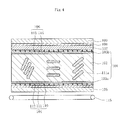
- Non-Patent Document 1 an AM type liquid crystal display device as shown in FIG. 4 is described.
- the liquid crystal layer 101 includes a liquid crystal molecular phase 102 formed of nematic liquid crystal, and a pair of alignment films 103a and 103b formed on the upper and lower ends of the liquid crystal molecular phase 102. Further, the AM substrate 104 and the first polarizing plate 105 are disposed on one main surface side of the liquid crystal layer 101, and the color filter 106, the second polarizing plate 107, and the transparent electrode 108 are disposed on the other main surface side. The transparent substrate 109 is sequentially arranged.
- pixel electrodes 111 are formed in a matrix on a transparent substrate 110, and a switching element 112 such as a thin film transistor (hereinafter referred to as “TFT”) is provided for each pixel electrode 111. It is configured to be able to be turned on / off.
- TFT thin film transistor
- the color filter 106 includes an RGB filter unit 114 that is divided into a red (R) filter unit, a green (G) filter unit, and a blue (B) filter unit for each pixel through a shielding layer 113 called a black matrix. have.
- the backlight unit 115 is arranged on the back side of the first polarizing plate 105 and is configured such that light is directly incident on the first polarizing plate 105.
- a white light source such as a cold cathode fluorescent tube, a white light emitting diode, or a mercury lamp is usually used.
- the white light source from the backlight unit 115 is linearly polarized by the first polarizing plate 105, the amount of light transmitted is controlled by the liquid crystal layer 101 according to the on / off operation of the switching element 112, and then Passing through the color filter 106 and the second polarizing plate 107, a color image is displayed on the display screen.
- polymer dispersed liquid crystal is also known as the liquid crystal constituting the liquid crystal molecular phase.
- the liquid crystal display device using this polymer dispersed liquid crystal disperses and scatters the liquid crystal in the polymer and electrically controls the scattering state.
- Patent Document 1 has a pixel including a polymer layer, a plurality of liquid crystal droplets dispersed in the polymer layer, and a plurality of quantum dots mixed in the liquid crystal droplets.
- the plurality of quantum dots of the pixel are excited by blue excitation light supplied from the outside of the polymer layer to generate light of a specific color corresponding to each of the quantum dots. Display panels have been proposed.
- each pixel has red, green, and blue sub-pixels, and the liquid crystal droplets of the red sub-pixels have quantum dots that are excited by blue light to generate red light.
- the liquid crystal droplets of the green sub-pixel have quantum dots that are excited by blue light to generate green light, and the liquid crystal droplets of the blue sub-pixel have no quantum dots.
- Patent Document 1 when a voltage is applied to a liquid crystal droplet, the liquid crystal in the liquid crystal droplet is aligned in a certain direction, and accordingly, the refractive index of the liquid crystal droplet and the refractive index of the polymer layer are the same. . When the light passes through the liquid crystal droplet, the quantum dots in the liquid crystal droplet are excited.
- the quantum dot is excited by blue wavelength light to generate red wavelength light
- the quantum dot is excited by blue wavelength light to generate green wavelength light. Therefore, only red light is radiated through the red sub-pixel, only green light is radiated through the green sub-pixel, and no blue dot is present in the blue sub-pixel, so that blue wavelength light is passed through and blue light is radiated. .
- Patent Document 1 since the liquid crystal droplets contain quantum dots that generate light of a specific color, color display is performed even without the color filter described in Non-Patent Document 1 (FIG. 4). In addition, since it is controlled based on the light scattering effect, it can operate as an optical shutter without the first polarizing plate. That is, in Patent Document 1, it is possible to omit a color filter and a polarizing plate.
- Patent Document 2 proposes a backlight unit member using quantum dots including a frame on which a blue light emitting element is mounted and a light transmission layer formed on the frame and containing quantum dots. Yes.
- blue LED a blue light emitting diode
- a light transmission layer containing quantum dots whereby blue light is white. It is trying to obtain a backlight unit member which is converted into light and is inexpensive and has good color reproducibility.
- JP 2010-191424 A (Claims 1 to 3, paragraphs [0033], [0038], [0039], etc.)
- JP 2013-539170 A (Claim 1, paragraph [0018], FIG. 3, 4 etc.)
- Non-Patent Document 1 (FIG. 4), only necessary color components of white light used as a light source pass through the color filter 106, and unnecessary color components are cut, so that light use efficiency is low. That is, for example, when the required color component is a blue component, only the blue component passes through the color filter 106, and the color gamut of the red component and the green component is cut and removed. It was.
- the color purity of the color filter 106 is usually increased to improve the color purity. .
- Non-Patent Document 1 since a white light source is used as the light source output from the backlight unit 115, the polarization control by the first polarizing plate 102 is not specialized for a specific color component, For this reason, the difference in contrast for each color component may be large.
- Non-Patent Document 1 since the light from the color filter 106 is polarized and output by the second polarizing plate 107, the viewing angle may be narrowed.
- polarized sunglasses are used in car navigation such as an automobile, there is a possibility that the user may recognize the image as a color tone different from the actual image.
- the conventional liquid crystal display device as described in Non-Patent Document 1 uses a white light source for the backlight unit 115, so that the light use efficiency is extremely low, and a desired contrast cannot be obtained. There are various problems such as narrow corners and inferior color visibility.
- Patent Document 1 does not require a color filter or a polarizing plate by configuring the liquid crystal molecular phase with a polymer-dispersed liquid crystal.
- the polarizing plate is omitted, there is a risk of lowering the contrast. That is, by omitting the polarizing plate, an image with sufficient brightness can be obtained when the switching element is on, but on the other hand, since the shutter effect by the polarizing plate cannot be obtained, it is difficult to control when the switching element is off, It is difficult to obtain a desired contrast, which may cause a decrease in contrast.
- Patent Document 2 uses a blue LED as a light source of a backlight unit, and converts blue light into white light in a light transmission layer. Therefore, white light is incident on the polarizing plate. It has the same problem as Non-Patent Document 1.
- a liquid crystal display device polarizes light output from a backlight unit with a first polarizing plate, supplies the light to a liquid crystal layer, and transmits light whose transmission is controlled by the liquid crystal layer.
- a liquid crystal display device that processes with a color filter and displays a color on a display screen, wherein the liquid crystal layer has a liquid crystal molecular phase composed of a nematic liquid crystal, and the backlight unit has a blue light emission source,
- the color filter includes a B filter portion, an R filter portion, and a G filter portion for each pixel, and the B filter portion is formed of a transparent polymer material in which a light scattering promoting material that promotes light scattering is dispersed.
- the R filter part and the G filter part are formed of a polymer material in which quantum dots emitting red and green light are dispersed, respectively, and the liquid crystal layer and the color filter
- the second polarizing plate is characterized by being interposed between.
- the blue component from the blue light source is output as it is from the B filter section, but is sufficiently scattered by the light scattering accelerator, so that almost no light loss due to polarized light occurs, and it is output in a state close to non-polarized light.
- the red component and the green component are color-converted (wavelength-converted) by the quantum dots contained in the R filter unit and the G filter unit, and are output from the R filter unit and the G filter unit.
- the second polarizing plate is interposed between the liquid crystal layer and the color filter, the light incident on the R filter unit and the G filter unit is polarized. Polarized light is absorbed by the quantum dots. Since light is emitted from the quantum dots at a solid angle of 4 ⁇ by photoluminescence, the light output from the R filter unit and the G filter unit has no polarization component and is output in a non-polarized state.
- the blue light emitting source is a blue LED.
- the light scattering accelerator is silica beads, titanium oxide, zirconium oxide, zinc oxide, aluminum oxide, barium sulfate, mica, diamond, glass, polymethyl methacrylate, It preferably contains at least one of poly (n-butyl methacrylate), polystyrene, silicone resin, and acrylic urethane.
- the quantum dots may include at least one element selected from the group consisting of Cd, Zn, Ga, In, Al, Sn, Ag, and Cu, and S, Se, Te, It is preferably composed of a combination of two or more elements including at least one selected from the group of O, P, As and N.
- the liquid crystal layer has a liquid crystal molecular phase made of nematic liquid crystal
- the backlight unit has a blue light emission source
- the color filter has a B filter for each pixel.
- Part, R filter part, and G filter part, and the B filter part is formed of a transparent polymer material in which a light scattering promoting material that promotes light scattering is dispersed
- the R filter part and the G filter part Is formed of a polymer material in which quantum dots emitting red and green light are dispersed
- a second polarizing plate is interposed between the liquid crystal layer and the color filter.
- the blue component from is directly output from the B filter unit, and the red and green components are color-converted (wavelength converted) by the quantum dots contained in the R and G filter units. It is outputted from the R filter unit and the G filter section.
- the blue component the blue light from the blue light source is used as it is, and for the red component or the green component, the blue component is changed to the red component or green via the respective quantum dots in the R filter unit or the G filter unit. Since color is output after being converted to component wavelengths, it is not necessary to remove color components in unnecessary wavelength ranges, and it is possible to improve light utilization efficiency even when nematic liquid crystal is used. Become. As a result, it is possible to obtain a liquid crystal display device having a desired brightness even when the light amount of the light source from the backlight unit is reduced as compared with the conventional liquid crystal display device as in Non-Patent Document 1, and lower consumption. An electric power liquid crystal display device can be realized.
- the wavelength band of light passing through the liquid crystal layer is only the blue component
- the retardation amount defining the phase difference between the first polarizing plate and the second polarizing plate to the blue component is increased. Can be improved.
- each color component passes through the color filter after passing through the second polarizing plate, the output light has no polarization component and is not polarized, has a good viewing angle, and uses polarized sunglasses. Even in this case, an image having good color visibility can be obtained.
- the liquid crystal has good contrast, is bright, has a sufficient viewing angle, good color visibility, and low power consumption.
- a display device can be obtained.
- FIG. 1 is a cross-sectional view schematically showing an embodiment of a liquid crystal display device according to the present invention. It is sectional drawing which shows an example of a blue light emitting diode. It is sectional drawing which shows the detail of a color filter. It is sectional drawing which shows the prior art example of a liquid crystal display device.
- FIG. 1 is a sectional view schematically showing one embodiment of an active matrix liquid crystal display (hereinafter referred to as “AM-LCD”) as a liquid crystal display device according to the present invention.
- A-LCD active matrix liquid crystal display
- the AM-LCD includes a backlight unit 1 that outputs a blue light source, and a polarizer (first polarization) that controls polarization so that only linearly polarized light passes through the blue light source output from the backlight unit 1.
- Plate) 2 an AM substrate 3 configured to be turned on / off for each pixel, a liquid crystal layer 4 that controls the transmission amount of light whose polarization is controlled by the polarizer 2, and a polarization axis that is the polarizer.
- An analyzer (second polarizing plate) 5 disposed so as to be orthogonal or parallel to the polarization axis 2, a color filter 6 that filters light transmitted through the liquid crystal layer 4, and an AM substrate 3.
- the counter substrate 7 is provided.
- the polarization axes of the polarizer 2 and the analyzer 5 are parallel to each other, it is a normally white type, which displays white when no electric field is applied to the liquid crystal layer 4 and displays black when an electric field is applied.
- normally black type and normally white type are liquid crystal operation modes (for example, TN (twisted nematic) mode, VA (vertical alignment) mode, IPS (in-plane switching) mode, STN (super twisted nematic) mode).
- TN twisted nematic
- VA vertical alignment
- IPS in-plane switching
- STN super twisted nematic
- Any type can be selected according to the present invention, and the present invention can be adapted to any type.
- the AM substrate 3 includes a first transparent substrate 9 made of alkali-free glass, extremely low alkali glass, or the like, and a pixel electrode 10 made of a transparent conductive film such as ITO is formed on the first transparent substrate 9.
- a switching element 11 is connected to each pixel electrode 10 in a matrix.
- TFTs or MIM (metal-insulator-metal) type thin film diodes (TFDs) usually made of amorphous silicon, polycrystalline silicon, oxide semiconductors mainly composed of In-Ga-Zn, or the like are used. Is used.
- the AM substrate 3 can be easily manufactured by repeatedly using a well-known CVD method, sputtering method, or photolithography technique.
- the liquid crystal layer 4 includes a liquid crystal molecular phase 12 made of nematic liquid crystal such as TN liquid crystal, VA liquid crystal, IPS liquid crystal, STN liquid crystal, and an alignment film 13a made of soluble polyimide formed on the upper and lower ends of the liquid crystal molecular phase 12. , 13b.
- a liquid crystal molecular phase 12 made of nematic liquid crystal such as TN liquid crystal, VA liquid crystal, IPS liquid crystal, STN liquid crystal
- an alignment film 13a made of soluble polyimide formed on the upper and lower ends of the liquid crystal molecular phase 12. , 13b.
- the counter substrate 7 includes a second transparent substrate 14 disposed to face the first transparent substrate 9, and a transparent electrode made of a transparent conductive film such as ITO formed on the back surface side of the second transparent substrate 14. 15.
- the backlight unit 1 is arranged on the back side of the polarizer 2 so that light from the blue light source is directly incident on the polarizer 2.
- the backlight unit 1 is an edge light system suitable for energy saving and thinning.
- the backlight unit 1 includes a light source unit 16 and a light guide mainly composed of an acrylic resin formed in a wedge shape that converts a point light source or a line light source output from the light source unit 16 into a surface light source.
- the light source unit 16 has a plurality of blue LEDs as blue light emitting sources. Specifically, blue LEDs are embedded in a package filled with resin and mounted on a substrate, and a plurality of such blue LEDs are provided in a row, thereby forming a light source unit 16.
- FIG. 2 is a cross-sectional view schematically showing an example of a blue LED.
- a buffer layer 21 made of GaN is formed on a substrate 20 such as Al 2 O 3 , and an n-type cladding layer 22 in which GaN is doped with Si is formed on the surface of the buffer layer 21.
- An active layer 23 and an n-type electrode 27 such as ITO are formed on the surface of the n-type cladding layer 22.
- a p-type cladding layer 24 in which GaN is doped with Mg is formed on the surface of the active layer 23, and a conductive layer 25 made of Ni, Au, or the like is formed on the surface of the p-type cladding layer 24, and A p-type electrode 26 made of Al or the like is formed on the conductive layer 25.
- the active layer 23 has a multiple quantum well type structure, in which barrier layers 28a to 28e made of GaN and well layers 29a to 29d made of In x Ga 1-x N are alternately stacked.
- the blue LED configured as described above, when a voltage is applied between the p-type electrode 26 and the n-type electrode 27, electrons and holes are generated in the well layers 29a to 29d sandwiched between the barrier layers 28a to 28e. It is confined and electron-hole recombination occurs, and emits blue light having a wavelength corresponding to the band gap of the well layers 29a to 29e, that is, a wavelength of about 470 nm.
- the color filter 6 includes an R filter unit, a G filter unit, and a B filter unit for each pixel, and enables RGB color display by these filtering operations.
- FIG. 3 is a cross-sectional view showing the configuration of the color filter 6 in units of pixels.
- the color filter 6 has a filtering portion 31 formed on a transparent substrate 30 such as a glass substrate.
- a black shielding layer 32 is arranged in a matrix to form a black matrix, and an R filter unit 33a, a G filter unit 33b, and a B filter 33c are divided through the shielding layer 32.
- the R filter unit 33a, the B filter unit 33b, and the G filter unit 33c form an RGB filter 33 in units of pixels.
- an overcoat layer 34 made of a transparent material such as an acrylic resin is formed on the surface of the filtering part 31, and the filtering part 31 is protected by the overcoat layer 34.
- the liquid crystal layer 4 is controlled with high accuracy so that the thickness including the overcoat layer 34 does not vary.
- the R filter part 33a and the G filter part 33b are such that quantum dots exhibiting red (wavelength: about 630 to 660 nm) and green (wavelength: about 520 to 540 nm) emission colors are dispersed in a polymer material.
- the quantum dot has a nano-order crystal grain size, and the wavelength varies depending on the crystal grain size due to the quantum size effect. Therefore, by using two types of quantum dots having different crystal grain sizes, the blue light output from the blue LED is color-converted (wavelength converted), and red light and green light can be output.
- Such a quantum dot is not particularly limited as long as it has a light emitting property.
- at least selected from the group of Cd, Zn, Ga, In, Al, Sn, Pb, Ag, and Cu at least selected from the group of Cd, Zn, Ga, In, Al, Sn, Pb, Ag, and Cu.
- a compound composed of one element and two or more elements including at least one element selected from the group of S, Se, Te, P, As, O, and N, such as CdS, CdSe, ZnSe, InGaSe or the like can be used.
- a light scattering promoting material that promotes light scattering is dispersed in a transparent polymer material, whereby the B filter portion 33c uses a blue light emitting source emitted from a blue LED as a blue component as it is. Output.
- the transparent polymer material for example, a methacrylic ester polymer material can be used.
- the light scattering promoting material is not particularly limited.
- inorganic materials such as silica beads, titanium oxide, zirconia oxide, zinc oxide, aluminum oxide, barium sulfate, mica, diamond, glass, etc.
- Fine scatterers made of materials and organic materials such as polymethyl methacrylate, poly-n-butyl methacrylate, polystyrene, silicone resin, and acrylic urethane can be used.
- silica beads can be preferably used.
- the color filter 6 can be easily manufactured using a well-known photolithography technique. That is, a photosensitive resist containing a black pigment is applied to the transparent substrate 30, exposed and developed using a photomask having a predetermined pattern, and patterned to form a matrix-shaped shielding layer 32. After that, similarly to the above, patterning is performed repeatedly using photolithography technology, sequentially forming the R filter portion 33a, the G filter portion 33b, and the B filter portion 33c, thereby forming the filtering portion 31, and thereafter An overcoat layer 34 is formed of an acrylic resin or the like on the surface of the filtering unit 31, whereby the color filter 6 can be easily manufactured.
- the display principle of the color filter 6 will be described in detail for the normally black type in which the liquid crystal operation mode is the TN mode. Note that even if the operation mode of the liquid crystal is the VA mode or the IPS mode, only the polarization control method is different, and the principle of making the polarized light incident on the liquid crystal layer 4 and outputting the unpolarized light is the same.
- the liquid crystal molecules corresponding to the R filter unit 33a are The liquid crystal molecules aligned in the horizontal direction and corresponding to the G filter portion 33b and the B filter portion 33 are aligned in the vertical direction.
- the blue light incident from the polarizer 2 is rotated along the liquid crystal molecules in the liquid crystal layer 4, and the polarization plane is rotated by 90 °. It is cut off and the display is black.
- the blue light incident from the polarizer 2 reaches the analyzer 5 while the polarization state is maintained by applying a voltage to the liquid crystal layer 4, and the blue light enters the polarization axis of the analyzer 5.
- the linearly polarized light is incident. Therefore, the light is transmitted through the analyzer 5 with almost no light loss, and is subjected to color conversion (wavelength conversion) by the R filter unit 33, whereby red is displayed on the display screen.
- the liquid crystal molecules corresponding to the G filter unit 33b when a voltage is applied to the liquid crystal molecules corresponding to the G filter unit 33b and no voltage is applied to the liquid crystal molecules corresponding to the R filter unit 33a and the B filter unit 33c, the liquid crystal molecules corresponding to the G filter unit 33b. Are aligned in the horizontal direction, and the liquid crystal molecules corresponding to the R filter portion 33a and the B filter portion 33c are aligned in the vertical direction.
- the blue light incident from the polarizer 2 rotates along the liquid crystal molecules in the liquid crystal layer 4, and the polarization plane rotates by 90 °. It is cut off and the display is black.
- the blue light incident from the polarizer 2 reaches the analyzer 5 while the polarization state is maintained by applying a voltage to the liquid crystal layer 4, and the polarization axis of the analyzer 5
- the linearly polarized light is incident. Therefore, the light is transmitted through the analyzer 5 with almost no light loss, and the G filter section 33b performs color conversion (wavelength conversion) so that blue light becomes green light, thereby displaying green on the display screen. .
- the liquid crystal molecules corresponding to the B filter unit 33c are The liquid crystal molecules aligned in the horizontal direction and corresponding to the R filter portion 33a and the B filter portion 33c are aligned in the vertical direction.
- the blue light incident from the polarizer 2 rotates along the liquid crystal molecules in the liquid crystal layer 4, and the polarization plane rotates by 90 °. It is cut off and the display is black.
- the blue light incident from the polarizer 2 reaches the analyzer 5 while the polarization state is maintained by applying a voltage to the liquid crystal layer 4, and the polarization axis of the analyzer 5 The linearly polarized light is incident. Therefore, the light is transmitted through the analyzer 5 and the B filter unit 33c with almost no light loss, whereby blue is displayed on the display screen.
- the backlight unit 1 includes the light source unit 16 having the blue LED
- the color filter 6 includes the R filter unit 33a, the G filter unit 33b, and the B filter unit 33c for each pixel.
- the B filter portion 33c is formed of a transparent polymer material in which a light scattering promoting material is dispersed
- the R filter portion 33a and the G filter portion 33b are dispersed with quantum dots that emit light in red and green, respectively.
- the analyzer 5 is formed between the liquid crystal layer 4 and the color filter 6 and is formed of a polymer material
- the blue component from the blue LED is directly transmitted from the B filter unit 33 c via the analyzer 5. Is output.
- the red component and the green component are color-converted (wavelength-converted) by the quantum dots contained in the R filter unit 33a and the G filter unit 33b, and are output from the R filter unit 33a and the G filter unit 33b.
- the B filter unit 33c outputs the blue light from the blue light source as it is, and for the red component or the green component, it passes through the respective quantum dots in the R filter unit 33a or the G filter unit 33b. Since the blue component is output after being converted to the red or green component wavelength, there is no need to remove unnecessary color components in the wavelength range unlike conventional white light sources, and this is the case when nematic liquid crystal is used. However, the light utilization efficiency can be improved at low cost.
- the contrast can be further improved by optimizing the retardation amount defining the phase difference generated between the polarizer 2 and the analyzer 5 to the blue component.
- the output light since the light passes through the color filter 6 after passing through the analyzer 5, the output light has no polarization component and is not polarized, has a good viewing angle, and has polarized sunglasses. Even if it is used, it is possible to obtain a desired image having good color visibility.
- Non-Patent Document 1 when the light utilization efficiency is compared between the present invention using a blue LED and the conventional example using a white light source, it is as follows.
- the light source output from the backlight unit is 50% of the amount of light cut by the polarizer, and the light loss caused when the light passing through the polarizer 2 passes through the liquid crystal layer 4 and the analyzer 5 Is 90%, and the aperture ratio of the liquid crystal layer is 50%.
- the light utilization efficiency about 2.5 ( ⁇ 11.3 / 4.45) times that of the conventional example can be obtained, and the power consumption of the backlight unit 1 can be greatly reduced. Therefore, for example, a secondary battery used in a smartphone or the like can be used continuously for a long time without frequently charging and discharging.
- the present invention is not limited to the above-described embodiment, and various modifications can be made without departing from the scope of the invention.
- the backlight unit 1 is configured by the edge light method, but it is needless to say that the present invention is not limited to this.
- the light utilization efficiency of the light source emitted from the backlight unit can be improved, the contrast is good, a sufficient viewing angle can be obtained, the color visibility is good, and A liquid crystal display device with low power consumption can be realized.
- Polarizer (first polarizing plate) 4 Liquid crystal layer 5 Analyzer (second polarizing plate) 6 Color filter 12 Liquid crystal molecular phase 16
- Light source part blue light source, blue LED
- R filter part 33b G filter part 33c B filter part
Landscapes
- Physics & Mathematics (AREA)
- General Physics & Mathematics (AREA)
- Optics & Photonics (AREA)
- Nonlinear Science (AREA)
- Liquid Crystal (AREA)
- Mathematical Physics (AREA)
- Chemical & Material Sciences (AREA)
- Crystallography & Structural Chemistry (AREA)
Abstract
光源部16から出力された光を偏光子2で偏光させて液晶層4に供給し、液晶層4で透過制御された光をカラーフィルタ6で処理し、表示画面上にカラー表示する。液晶層4はネマティック系液晶からなる液晶分子相12を有する。光源部16は青色LEDを有し、カラーフィルタ6は、画素毎に青色フィルタ部、赤色フィルタ部、及び緑色フィルタ部を備えている。青色フィルタ部は光の散乱を促進する光散乱促進材を分散させた透明性高分子材料で形成され、赤色フィルタ部及び緑色フィルタ部は赤色及び緑色にそれぞれ発光する量子ドットを分散させた高分子材料で形成されている。液晶層4とカラーフィルタ6との間に検光子5が介在されている。これにより低コストで光利用効率を向上させることができ、コントラストが良好で十分な視野角を有し、カラー視認性も良好な液晶表示装置を実現する。
Description
本発明は、液晶表示装置に関する。
液晶表示装置は、軽量で薄型化が可能であり、低消費電力であることから、テレビ受像機、パーソナルコンピュータ、携帯端末等の各種電子機器に広く使用されている。
この種の液晶表示装置のうち、アクティブマトリックス(以下、「AM」という。)タイプと呼称される液晶表示装置が、今日では広く普及している。このAMタイプの液晶表示装置は、印加電圧の保持機能を有するスイッチング素子を画素毎に配し、これら各画素をオン・オフ駆動させて画像をカラー表示するものであり、コントラストやレスポンス等が良好で大容量表示が可能である。
そして、非特許文献1には、図4に示すようなAMタイプの液晶表示装置が記載されている。
この液晶表示装置は、液晶層101が、ネマティック液晶で形成された液晶分子相102と、該液晶分子相102の上端及び下端に形成された一対の配向膜103a、103bとを有している。また、液晶層101の一方の主面側にはAM基板104及び第1の偏光板105が配されると共に、他方の主面側にはカラーフィルタ106、第2の偏光板107、透明電極108及び透明基板109が順次配されている。
AM基板104は、透明基板110上に画素電極111がマトリックス状に形成されると共に、薄膜トランジスタ(以下、「TFT」という。)等のスイッチング素子112が前記画素電極111毎に設けられ、画素毎にオン・オフ駆動可能となるように構成されている。
また、カラーフィルタ106は、ブラックマトリックスと称される遮蔽層113を介して画素毎に赤色(R)フィルタ部、緑色(G)フィルタ部、青色(B)フィルタ部に区分されたRGBフィルタ部114を有している。
バックライトユニット115は、第1の偏光板105の裏面側に配され、光が第1の偏光板105に直接入射するように構成されている。バックライトユニット115から発する光源には、通常、冷陰極蛍光管、白色発光ダイオード、水銀ランプ等の白色光源が使用されている。
すなわち、バックライトユニット115からの白色光源は、第1の偏光板105で直線偏光に偏光され、液晶層101でスイッチング素子112のオン・オフ動作に応じて光の透過量が制御され、その後、カラーフィルタ106及び第2の偏光板107を通過し、これにより表示画面にはカラー画像が表示される。
また、液晶分子相を構成する液晶としては、上述したネマテッィク液晶の他、高分子分散型液晶も知られている。
この高分子分散型液晶を使用した液晶表示装置は、高分子中に液晶を分散させて散乱させ、その散乱状態を電気的に制御している。
例えば、特許文献1には、高分子層と、前記高分子層内に分散された複数の液晶液滴と、前記液晶液滴の内部に混合されている複数の量子ドットとを備える画素を有し、当該画素の前記複数の量子ドットは、前記高分子層の外部から供給される青色の励起光により励起されてそれぞれの前記量子ドットに応じた特定の色の光を発生させる高分子分散型ディスプレイパネルが提案されている。
この特許文献1では、1つの画素毎に赤色、緑色、青色の各サブ画素をそれぞれ有し、赤色サブ画素の液晶液滴は、青色光により励起されて赤色光を発生させる量子ドットを有し、緑色サブ画素の液晶液滴は、青色光により励起されて緑色光を発生させる量子ドットを有し、青色サブ画素の液晶液滴は、量子ドットを有さないように構成されている。この特許文献1では、液晶液滴に電圧が印加されると、液晶液滴内の液晶が一定の方向に整列され、それに伴い液晶液滴の屈折率とポリマー層の屈折率とが同一になる。そして、光が液晶液滴を通過する際に液晶液滴内の量子ドットが励起される。例えば、赤色サブ画素では、量子ドットが青色波長の光により励起されて赤色波長の光を発生させ、緑色サブ画素では、量子ドットが青色波長の光により励起されて緑色波長光を発生させる。したがって、赤色サブ画素を通じては赤色光のみ放射され、緑色サブ画素を通じては緑色光のみ放射され、青色サブ画素には量子ドットが存在しないことから青色波長光がそのまま通過し、青色光が放射される。
このように特許文献1では、特定色の光を発生させる量子ドットが液晶液滴に含有されていることから、非特許文献1(図4)に記載されたカラーフィルタがなくてもカラー表示することができ、また光散乱効果に基づいて制御しているので第1の偏光板を有さなくても光シャッタとして動作できる。すなわち、特許文献1では、カラーフィルタや偏光板を省略することが可能である。
一方、バックライトユニットに内蔵される光源についても、上述した白色光源の他、青色光源を使用した技術が、従来より知られている。
例えば、特許文献2には、青色発光素子が実装されたフレームと、前記フレーム上に形成され、量子ドットが含有された光透過層を含む量子ドットを用いたバックライトユニット用部材が提案されている。
この特許文献2では、青色発光ダイオード(以下、「青色LED」という。)を光源に使用し、青色LEDからの青色光を量子ドットを含有した光透過層に透過させ、これにより青色光を白色光に変換し、安価で色再現性の良好なバックライトユニット用部材を得ようとしている。
松本正一著、「液晶ディスプレイ技術-アクティブマトリクスLCD-」、産業図書株式会社、1997年11月14日第2版、pp.179~180等
非特許文献1(図4)では、光源に使用される白色光のうち、必要な色成分のみがカラーフィルタ106を通過し、不必要な色成分はカットされるため、光利用効率が低い。すなわち、例えば必要な色成分が青色成分の場合、青色成分のみがカラーフィルタ106を通過し、赤色成分や緑色成分の色域はカットされて除去されるため、光利用効率が低いという問題があった。
また、非特許文献1のような従来の液晶表示装置では、各画素を通過する光の波長域が広いことから、通常、カラーフィルタ106の色材濃度を高くして色純度を向上させている。
しかしながら一方で、色材濃度を高くすると光透過率の低下を招き、このため光利用効率の更なる低下を招き、消費電力も大きくなる。
また、非特許文献1では、バックライトユニット115から出力する光源に白色光源を使用していることから、第1の偏光板102による偏光制御についても特定の色成分に特化したものでなく、このため色成分毎のコントラストの差が大きくなるおそれがある。
さらに、非特許文献1では、カラーフィルタ106からの光が、第2の偏光板107により偏光して出力されることから、視野角が狭くなるおそれがある。また、自動車等のカーナビゲーションで偏光サングラスを使用した場合は、ユーザには実際の画像と色調が異なる画像として認識されてしまうおそれがある。
このように非特許文献1のような従来の液晶表示装置は、バックライトユニット115に白色光源を使用しているため、光利用効率が極めて低く、所望のコントラストを得ることができず、また視野角も狭く、カラー視認性にも劣るおそれがある等、種々の問題がある。
一方、特許文献1は、液晶分子相を高分子分散型液晶で構成することにより、カラーフィルタや偏光板を不要としているが、偏光板を省略した場合にはコントラストの低下を招くおそれがある。すなわち、偏光板を省略することによりスイッチング素子のオン時には十分な明度の画像を得ることができるが、一方で偏光板によるシャッタ効果を得ることができないため、スイッチング素子のオフ時の制御が難しく、所望のコントラストを得るのが困難であり、コントラストの低下を招くおそれがある。
また、特許文献2は、バックライトユニットの光源に青色LEDを使用し、光透過層で青色光を白色光に変換しているため、偏光板には白色光が入射されることとなり、したがって上述した非特許文献1と同様の課題を有する。
本発明はこのような事情に鑑みなされたものであって、低コストで光利用効率を向上させることができ、コントラストが良好で明るく、十分な視野角を有し、カラー視認性も良好で、かつ消費電力の低い液晶表示装置を提供することを目的とする。
上記目的を達成するために本発明に係る液晶表示装置は、バックライトユニットから出力された光を第1の偏光板で偏光させて液晶層に供給し、該液晶層で透過制御された光をカラーフィルタで処理し、表示画面上にカラー表示する液晶表示装置であって、前記液晶層が、ネマティック系液晶からなる液晶分子相を有すると共に、前記バックライトユニットが、青色発光源を有し、前記カラーフィルタは、画素毎にBフィルタ部、Rフィルタ部、及びGフィルタ部を備え、前記Bフィルタ部は光の散乱を促進する光散乱促進材を分散させた透明性高分子材料で形成されると共に、Rフィルタ部及びGフィルタ部は、赤色及び緑色にそれぞれ発光する量子ドットを分散させた高分子材料で形成され、かつ、前記液晶層と前記カラーフィルタとの間に第2の偏光板が介在されていることを特徴としている。
これにより青色発光源からの青色成分は、そのままBフィルタ部から出力されるが、光散乱促進材により十分に散乱されることから、偏光による光損失は殆ど生じず、無偏光に近い状態で出力される。また、赤色成分及び緑色成分はRフィルタ部及びGフィルタ部に含有された量子ドットにより色変換(波長変換)され、Rフィルタ部及びGフィルタ部から出力される。さらに、液晶層とカラーフィルタとの間に第2の偏光板を介在させているので、Rフィルタ部及びGフィルタ部に入射する光は偏光しているが、これらRフィルタ部及びGフィルタ部内の量子ドットにより偏光が吸収される。そして、フォトルミネッセンスによって、立体角4πで量子ドットから光が放出されることから、Rフィルタ部及びGフィルタ部から出力される光は、偏光成分を有さず、無偏光状態で出力される。
また、本発明の液晶表示装置は、前記青色発光源が、青色LEDであるのが好ましい。
さらに、本発明の液晶表示装置は、前記光散乱促進材が、シリカビーズ、チタン酸化物、ジルコニウム酸化物、亜鉛酸化物、アルミニウム酸化物、硫酸バリウム、マイカ、ダイヤモンド、ガラス、ポリメタクリル酸メチル、ポリメタクリル酸n-ブチル、ポリスチレン、シリコーン樹脂、アクリルウレタンのうちの少なくとも1種を含むのが好ましい。
また、本発明の液晶表示装置は、前記量子ドットが、Cd、Zn、Ga、In、Al、Sn、Ag、及びCuの群から選択された少なくとも1種の元素と、S、Se、Te、O、P、As及びNの群から選択された少なくとも1種とを含む2種以上の元素の組み合わせからなるのが好ましい。
本発明の液晶表示装置によれば、前記液晶層が、ネマティック系液晶からなる液晶分子相を有すると共に、前記バックライトユニットが、青色発光源を有し、前記カラーフィルタは、画素毎にBフィルタ部、Rフィルタ部、及びGフィルタ部を備え、前記Bフィルタ部は光の散乱を促進する光散乱促進材を分散させた透明性高分子材料で形成されると共に、Rフィルタ部及びGフィルタ部は、赤色及び緑色にそれぞれ発光する量子ドットを分散させた高分子材料で形成され、かつ、前記液晶層と前記カラーフィルタとの間に第2の偏光板が介在されているので、青色発光源からの青色成分は、そのままBフィルタ部から出力され、赤色成分及び緑色成分はRフィルタ部及びGフィルタ部に含有された量子ドットにより色変換(波長変換)され、Rフィルタ部及びGフィルタ部からそれぞれ出力される。
このように青色成分については、青色発光源からの青色光をそのまま使用し、赤色成分又は緑色成分については、Rフィルタ部又はGフィルタ部におけるそれぞれの量子ドットを介して青色成分から赤色成分又は緑色成分の波長に変換して色出力していることから、不要な波長域の色成分を除去する必要がなく、ネマテッィク系液晶を使用した場合であっても光利用効率を向上させることが可能となる。その結果、非特許文献1のような従来の液晶表示装置に比べ、バックライトユニットからの光源の光量を低下させても、所望の明るさを有する液晶表示装置を得ることができ、より低消費電力の液晶表示装置を実現することが可能となる。
また、液晶層を通過する光の波長帯が青色成分のみであることから、第1の偏光板と第2の偏光板の間の位相差を規定するリタデーション量を青色成分に最適化することにより、コントラストを改善することができる。
また、第2の偏光板を通過した後、各色成分はカラーフィルタを通過するので、出力される光は偏光成分を有さず無偏光となり、良好な視野角を有し、偏光サングラスを使用した場合であっても、良好なカラー視認性を有する画像を得ることができる。
このように本発明によれば、低コストで光利用効率を向上させることができるので、コントラストが良好で明るく、十分な視野角を有し、カラー視認性も良好で、かつ消費電力も低い液晶表示装置を得ることができる。
次に、本発明の実施の形態を詳説する。
図1は、本発明に係る液晶表示装置としてのアクティブマトリックス液晶ディスプレイ(以下、「AM-LCD」という。)の一実施の形態を模式的に示す断面図である。
このAM-LCDは、青色発光源を出力するバックライトユニット1と、該バックライトユニット1から出力された青色発光源のうち直線偏光のみが通過するように偏光制御する偏光子(第1の偏光板)2と、各画素毎にオン・オフ駆動するように構成されたAM基板3と、偏光子2により偏光制御された光の透過量を制御する液晶層4と、偏光軸が前記偏光子2の偏光軸と直交又は平行となるように配された検光子(第2の偏光板)5と、液晶層4を透過した光をフィルタリングするカラーフィルタ6と、AM基板3と対向状に配された対向基板7とを備えている。
尚、偏光子2と検光子5の偏光軸が直交している場合は、ノーマリーブラックタイプとなり、液晶層4に電界が印加されない時は黒表示となり、電界が印加されると白表示となる。
一方、偏光子2と検光子5の偏光軸が平行している場合は、ノーマリーホワイトタイプとなり、液晶層4に電界が印加されない時に白表示となり、電界が印加されると黒表示となる。
これらノーマリーブラックタイプ及びノーマリーホワイトタイプは、液晶の動作モード(例えば、TN(ねじれネマティック)モード、VA(垂直配向)モード、IPS(面内スイッチング)モード、STN(超ねじれネマティック)モード等)に応じて任意に選ぶことができ、本発明ではいずれのタイプにも対応可能となるように構成されている。
AM基板3は、無アルカリガラスや極低アルカリガラス等で形成された第1の透明基板9を備えると共に、前記第1の透明基板9上にはITO等の透明導電膜からなる画素電極10がマトリックス状に配され、かつ各画素電極10にはスイッチング素子11がそれぞれ接続されている。スイッチング素子11には、通常、非晶質シリコンや多結晶シリコン、In-Ga-Znを主成分とした酸化物半導体等からなるTFTやMIM(metal-insulator-metal)形の薄膜ダイオード(TFD)が使用される。
尚、このAM基板3は、周知のCVD法やスパッタリング法、更にはフォトリソグラフィ技術を繰り返し使用することにより容易に作製することができる。
液晶層4は、TN液晶、VA液晶、IPS液晶、STN液晶等のネマティック系液晶からなる液晶分子相12と、該液晶分子相12の上端及び下端に形成された可溶性ポリイミド等からなる配向膜13a、13bとを有している。
対向基板7は、第1の透明基板9と対向状に配された第2の透明基板14と、該第2の透明基板14の裏面側に形成されたITO等の透明導電膜からなる透明電極15とを有している。
そして、バックライトユニット1は、青色発光源からの光が偏光子2に直接入射されるように偏光子2の裏面側に配されている。
本実施の形態では、バックライトユニット1は、省エネ・薄型化に適したエッジライト方式とされている。
具体的には、このバックライトユニット1は、光源部16と、該光源部16から出力される点光源又は線光源を面光源に変換する楔形状に形成されたアクリル樹脂等を主体とした導光板17と、光源部16からの光を反射させて導光板17側に案内する反射板18と、導光板17に案内された光を拡散させるアクリル樹脂等で形成された拡散板19とを備えている。
そして、光源部16は、青色発光源としての青色LEDを複数有している。具体的には、青色LEDは、樹脂が充填されたパッケージ内に埋め込まれて基板上に実装されており、斯かる青色LEDが複数列設され、これにより光源部16が形成されている。
図2は、青色LEDの一例を模式的に示す断面図である。
青色LEDは、Al2O3等の基板20上にGaNからなるバッファ層21が形成され、該バッファ層21の表面にはGaNにSiをドープしたn型クラッド層22が形成されている。n型クラッド層22の表面には活性層23及びITO等のn型電極27が形成されている。さらに、活性層23の表面にはGaNにMgをドープしたp型クラッド層24が形成されると共に、該p型クラッド層24の表面にはNiやAu等からなる導電層25が形成され、かつ、導電層25上にはAl等のp型電極26が形成されている。
また、活性層23は、多重量子井戸型構造とされ、GaNからなる障壁層28a~28eと、InxGa1-xNからなる井戸層29a~29dとが交互に積層されている。
このように構成された青色LEDでは、p型電極26とn型電極27との間に電圧が印加されると、障壁層28a~28eに挟まれた井戸層29a~29dに電子及び正孔が閉じ込められ、電子-正孔の再結合が生じ、井戸層29a~29eのバンドギャップに相当する波長、すなわち約470nmの波長を有する青色光を発する。
また、カラーフィルタ6は、1つの画素毎にRフィルタ部、Gフィルタ部、及びBフィルタ部を備えており、これらのフィルタリング作用によりRGBのカラー表示を可能にしている。
図3は、カラーフィルタ6の画素単位の構成を示す断面図である。
すなわち、カラーフィルタ6は、ガラス基板等の透明基板30上にフィルタリング部31が形成されている。このフィルタリング部31は、黒色の遮蔽層32がマトリックス状に配されてブラックマトリックスを形成すると共に、Rフィルタ部33a、Gフィルタ部33b、及びBフィルタ33cが遮蔽層32を介して区分され、これらRフィルタ部33a、Bフィルタ部33b、及びGフィルタ部33cにより画素単位でRGBフィルタ33を形成している。
また、フィルタリング部31の表面には、アクリル樹脂等の透明材料からなるオーバーコート層34が形成されており、フィルタリング部31はオーバーコート層34によって保護されている。液晶層4は、オーバーコート層34を含む厚みにバラツキが生じないように高精度に制御される。
RGBフィルタ33のうち、Rフィルタ部33a及びGフィルタ部33bは、赤色(波長:約630~660nm)及び緑色(波長:約520~540nm)の発光色を示す量子ドットが高分子材料中に分散されている。すなわち、量子ドットはナノオーダーの結晶粒径を有しており、量子サイズ効果により結晶粒径の大きさに応じて波長が変動する。したがって、結晶粒径の異なる2種類の量子ドットを使用することにより、青色LEDから出力される青色光が色変換(波長変換)され、赤色光や緑色光を出力することができる。
このような量子ドットとしては、発光性を有していれば特に限定されるものではなく、例えば、Cd、Zn、Ga、In、Al、Sn、Pb、Ag、Cuの群から選択された少なくとも1種の元素と、S、Se、Te、P、As、O、Nの群から選択された少なくとも1種の元素を含む2種以上の元素で構成された化合物、例えばCdS、CdSe、ZnSe、InGaSe等を使用することができる。
また、Bフィルタ部33cは、光散乱を促進させる光散乱促進材が透明性高分子材料に分散されており、これによりBフィルタ部33cは、青色LEDから発せられる青色発光源をそのまま青色成分として出力している。
ここで、透明性高分子材料としては、例えば、メタアクリル酸エステル系高分子材料を使用することができる。
また、光散乱促進材についても、特に限定されるものではなく、例えば、シリカビーズ、チタン酸化物、ジルコニア酸化物、亜鉛酸化物、アルミニウム酸化物、硫酸バリウム、マイカ、ダイヤモンド、ガラス等の無機系材料や、ポリメタクリル酸メチル、ポリメタクリル酸n-ブチル、ポリスチレンン、シリコーン樹脂、アクリルウレタンなどの有機系材料等からなる微小散乱体を使用することができる。これら微小散乱体の中ではシリカビーズを好んで使用することができる。
尚、このカラーフィルタ6は、周知のフォトリソグラフィ技術を使用して容易に作製することができる。すなわち、透明基板30に黒色顔料を含有した感光性レジストを塗布し、所定パターンのフォトマスクを使用して露光・現像を行い、パターニングしてマトリックス状の遮蔽層32を形成する。その後、上述と同様、フォトリソグラフィ技術を繰り返し使用してパターンニングし、順次Rフィルタ部33a、Gフィルタ部33b、Bフィルタ部33cを形成し、これによりフィルタリング部31を形成する、そしてこの後、フィルタリング部31の表面にアクリル樹脂等でオーバーコート層34を形成し、これによりカラーフィルタ6を容易に作製することができる。
次に、液晶の動作モードがTNモードのノーマリーブラックタイプについて、カラーフィルタ6の表示原理を詳述する。尚、液晶の動作モードがVAモードやIPSモードであっても、偏光の制御方法が異なるのみであり、偏光を液晶層4に入射し、無偏光状態の光を出力させる原理は同様である。
例えば、Rフィルタ部33aに対応する液晶分子に電圧が印加され、Gフィルタ部33b及びBフィルタ部33に対応する液晶分子に電圧が印加されなかった場合、Rフィルタ部33aに対応する液晶分子は水平方向に配向し、Gフィルタ部33b及びBフィルタ部33に対応する液晶分子は垂直方向に配向する。そして、Gフィルタ部33b及びBフィルタ部33cでは、偏光子2から入射した青色光は、液晶層4で液晶分子に沿って偏光が旋回し、偏光面が90°回転することによって検光子5で遮断され、黒表示となる。一方、Rフィルタ部33aでは、偏光子2から入射した青色光は、液晶層4に電圧が印加されることで偏光状態が維持されたまま検光子5に到達し、検光子5の偏光軸に沿った直線偏光が入射される。したがって、光損失が殆ど生じることなく検光子5を透過し、Rフィルタ部33で色変換(波長変換)され、これにより表示画面には赤色が表示される。
同様に、Gフィルタ部33bに対応する液晶分子に電圧が印加され、Rフィルタ部33a及びBフィルタ部33cに対応する液晶分子に電圧が印加されなかった場合、Gフィルタ部33bに対応する液晶分子は水平方向に配向し、Rフィルタ部33a及びBフィルタ部33cに対応する液晶分子は垂直方向に配向する。そして、Rフィルタ部33a及びBフィルタ部33cでは、偏光子2から入射した青色光は、液晶層4で液晶分子に沿って偏光が旋回し、偏光面が90°回転することによって検光子5で遮断され、黒表示となる。一方、Gフィルタ部33bでは、偏光子2から入射した青色光は、液晶層4に電圧が印加されることで偏光状態が維持されたまま検光子5に到達し、検光子5の偏光軸に沿った直線偏光が入射される。したがって、光損失が殆ど生じることなく検光子5を透過し、前記Gフィルタ部33bで青色光が緑色光となるように色変換(波長変換)され、これにより表示画面には緑色が表示される。
また、Bフィルタ部33cに対応する液晶分子に電圧が印加され、Rフィルタ部33a及びGフィルタ部33bに対応する液晶分子に電圧が印加されなかった場合、Bフィルタ部33cに対応する液晶分子は水平方向に配向し、Rフィルタ部33a及びBフィルタ部33cに対応する液晶分子は垂直方向に配向する。そして、Rフィルタ部33a及びBフィルタ部33cでは、偏光子2から入射した青色光は、液晶層4で液晶分子に沿って偏光が旋回し、偏光面が90°回転することによって検光子5で遮断され、黒表示となる。一方、Bフィルタ部33cでは、偏光子2から入射した青色光は、液晶層4に電圧が印加されることで偏光状態が維持されたまま検光子5に到達し、検光子5の偏光軸に沿った直線偏光が入射される。したがって、光損失が殆ど生じることなく検光子5及びBフィルタ部33cを透過し、これにより表示画面には青色が表示される。
このように本実施の形態では、バックライトユニット1が、青色LEDを有する光源部16を備え、カラーフィルタ6は、画素毎にRフィルタ部33a、Gフィルタ部33b、及びBフィルタ部33cを有し、Bフィルタ部33cは光散乱促進材を分散させた透明性高分子材料で形成されると共に、Rフィルタ部33a及びGフィルタ部33bは、赤色及び緑色にそれぞれ発光する量子ドットを分散させた高分子材料で形成され、かつ、液晶層4とカラーフィルタ6との間に検光子5が介在されているので、青色LEDからの青色成分は、検光子5を介してBフィルタ部33cからそのまま出力される。また、赤色成分及び緑色成分はRフィルタ部33a及びGフィルタ部33bに含有された量子ドットにより色変換(波長変換)され、Rフィルタ部33a及びGフィルタ部33bから出力される。
すなわち、青色成分については、Bフィルタ部33cは、青色発光源からの青色光をそのまま出力し、赤色成分又は緑色成分については、Rフィルタ部33a又はGフィルタ部33bにおけるそれぞれの量子ドットを介して青色成分から赤色成分又は緑色成分の波長に変換して出力されることから、従来の白色光源のように不要な波長域の色成分を除去する必要がなく、ネマテッィク系液晶を使用した場合であっても低コストで光利用効率を向上させることが可能となる。
また、本実施の形態では、液晶層4を透過する光の波長帯が青色成分のみであることから、VA液晶、IPS液晶などの複屈折が直接的に遮光・透光性能に影響を及ぼす動作モードでは、偏光子2と検光子5との間で生じる位相差を規定するリタデーション量を青色成分に最適化することにより、コントラストをより改善することができる。
また、本実施の形態では、検光子5を通過した後、カラーフィルタ6を通過するので、出力される光は偏光成分を有さず無偏光となり、良好な視野角を有し、偏光サングラスを使用した場合であっても、良好なカラー視認性を有する所望の画像を得ることができる。
因みに、青色LEDを使用した本発明と白色光源を使用した従来例(非特許文献1)とで光利用効率を比較すると、以下のようになる。
本発明及び従来例において、バックライトユニットから出力される光源が偏光子でカットされる光量を50%、偏光子2を通過した光が液晶層4及び検光子5を通過する際に生じる光損失を90%、液晶層の開口率を50%と仮定する。
白色光源を使用した従来例に特有の損失として、カラーフィルタに使用される色素の吸収による光損失、及び白色光からRGB各色への色変換時における他成分のカットによる光損失がある。後者は33%であるから、前者を60%とすると、RGBの各色成分当たりの光利用効率は、4.45%(=(0.50×0.90×0.50×0.60×0.33)×100)となる。
一方、本発明の場合、青色成分については、青色LEDの発光源をそのまま使用することから、色変換による損失は生じず、光散乱促進剤による散乱損失のみである。したがって、この散乱損失を80%としても、青色成分に対する光利用効率は、18%(=(0.50×0.90×0.50×0.80)×100)となる。
また、赤色成分及び緑色成分については、フォトルミネッセンスにより立体角4πで光が放出されることから、カラーフィルタによる損失は、反射損失を含めても50%程度と推測される。したがって、量子ドットの青色から赤色及び緑色への色変換(波長変換)による損失を70%とすると、赤色成分及び緑色成分に対する光利用効率は、それぞれ7.9%(=(0.50×0.90×0.50×0.50×0.70)×100)となる。
したがって、本発明では、光利用効率は、平均値で11.3%(=(18+7.9+7.9)/3)となる。
このように本発明は、従来例の約2.5(≒11.3/4.45)倍の光利用効率を得ることができ、バックライトユニット1の消費電力を大幅に低減できる。したがって、例えば、スマートフォン等で使用される二次電池の充放電を頻繁に行なうことなく長時間連続して使用することが可能となる。
尚、本発明は上記実施の形態に限定されるものではなく、要旨を逸脱しない範囲で種々の変形が可能であるのはいうまでもない。例えば、上記実施の形態では、バックライトユニット1をエッジライト方式で構成しているが、これに限定されるものでないのはいうまでもない。
ネマティック系液晶を使用しても、バックライトユニットから発せられる光源の光利用効率を向上させることができ、コントラストが良好で、十分な視野角を得ることができ、カラー視認性も良好で、かつ消費電力も低い液晶表示装置を実現できる。
1 バックライトユニット
2 偏光子(第1の偏光板)
4 液晶層
5 検光子(第2の偏光板)
6 カラーフィルタ
12 液晶分子相
16 光源部(青色発光源、青色LED)
33a Rフィルタ部
33b Gフィルタ部
33c Bフィルタ部
2 偏光子(第1の偏光板)
4 液晶層
5 検光子(第2の偏光板)
6 カラーフィルタ
12 液晶分子相
16 光源部(青色発光源、青色LED)
33a Rフィルタ部
33b Gフィルタ部
33c Bフィルタ部
Claims (4)
- バックライトユニットから出力された光を第1の偏光板で偏光させて液晶層に供給し、該液晶層で透過制御された光をカラーフィルタで処理し、表示画面上にカラー表示する液晶表示装置であって、
前記液晶層が、ネマティック系液晶からなる液晶分子相を有すると共に、
前記バックライトユニットが、青色発光源を有し、
前記カラーフィルタは、画素毎に青色フィルタ部、赤色フィルタ部、及び緑色フィルタ部を備え、前記青色フィルタ部は光の散乱を促進する光散乱促進材を分散させた透明性高分子材料で形成されると共に、赤色フィルタ部及び緑色フィルタ部は、赤色及び緑色にそれぞれ発光する量子ドットを分散させた高分子材料で形成され、
かつ、前記液晶層と前記カラーフィルタとの間に第2の偏光板が介在されていることを特徴とする液晶表示装置。 - 前記青色発光源は、青色発光ダイオードであることを特徴とする請求項1記載の液晶表示装置。
- 前記光散乱促進材は、シリカビーズ、チタン酸化物、ジルコニウム酸化物、亜鉛酸化物、アルミニウム酸化物、硫酸バリウム、マイカ、ダイヤモンド、ガラス、ポリメタクリル酸メチル、ポリメタクリル酸n-ブチル、ポリスチレン、シリコーン樹脂、アクリルウレタンのうちの少なくとも1種を含むことを特徴とする請求項1又は請求項2記載の液晶表示装置。
- 前記量子ドットは、Cd、Zn、Ga、In、Al、Sn、Ag、及びCuの群から選択された少なくとも1種の元素と、S、Se、Te、O、P、As及びNの群から選択された少なくとも1種の元素を含む2種以上の元素の組み合わせで構成されていることを特徴とする請求項1乃至請求項3のいずれかに記載の液晶表示装置。
Applications Claiming Priority (2)
| Application Number | Priority Date | Filing Date | Title |
|---|---|---|---|
| JP2015078368 | 2015-04-07 | ||
| JP2015-078368 | 2015-04-07 |
Publications (1)
| Publication Number | Publication Date |
|---|---|
| WO2016163196A1 true WO2016163196A1 (ja) | 2016-10-13 |
Family
ID=57072535
Family Applications (1)
| Application Number | Title | Priority Date | Filing Date |
|---|---|---|---|
| PCT/JP2016/057331 Ceased WO2016163196A1 (ja) | 2015-04-07 | 2016-03-09 | 液晶表示装置 |
Country Status (1)
| Country | Link |
|---|---|
| WO (1) | WO2016163196A1 (ja) |
Cited By (1)
| Publication number | Priority date | Publication date | Assignee | Title |
|---|---|---|---|---|
| JP2019168511A (ja) * | 2018-03-22 | 2019-10-03 | Dic株式会社 | 液晶表示素子及び液晶表示装置 |
Citations (2)
| Publication number | Priority date | Publication date | Assignee | Title |
|---|---|---|---|---|
| JP2014026167A (ja) * | 2012-07-27 | 2014-02-06 | Sharp Corp | 光学基板の製造方法、光学基板、光出射装置、表示装置および照明装置。 |
| WO2015045735A1 (ja) * | 2013-09-30 | 2015-04-02 | 富士フイルム株式会社 | 表示装置 |
-
2016
- 2016-03-09 WO PCT/JP2016/057331 patent/WO2016163196A1/ja not_active Ceased
Patent Citations (2)
| Publication number | Priority date | Publication date | Assignee | Title |
|---|---|---|---|---|
| JP2014026167A (ja) * | 2012-07-27 | 2014-02-06 | Sharp Corp | 光学基板の製造方法、光学基板、光出射装置、表示装置および照明装置。 |
| WO2015045735A1 (ja) * | 2013-09-30 | 2015-04-02 | 富士フイルム株式会社 | 表示装置 |
Cited By (1)
| Publication number | Priority date | Publication date | Assignee | Title |
|---|---|---|---|---|
| JP2019168511A (ja) * | 2018-03-22 | 2019-10-03 | Dic株式会社 | 液晶表示素子及び液晶表示装置 |
Similar Documents
| Publication | Publication Date | Title |
|---|---|---|
| KR102373327B1 (ko) | 액정 표시 장치 및 그 구동 방법 | |
| US9170453B2 (en) | Liquid crystal display panel including photo conversion layer and liquid crystal display device | |
| CN106291943B (zh) | 一种显示面板及显示装置 | |
| CN103135281B (zh) | 液晶显示装置 | |
| CN107918233B (zh) | 一种显示装置 | |
| US9995964B2 (en) | Liquid crystal display panel and display device | |
| CN106990604B (zh) | 一种液晶面板、显示模组及显示装置 | |
| CN104360540A (zh) | 一种显示装置 | |
| WO2018076948A1 (zh) | 显示面板和显示装置 | |
| CN107817629A (zh) | 一种液晶显示装置 | |
| CN104330918A (zh) | 一种显示面板和显示装置 | |
| WO2019218984A1 (zh) | 透明显示面板和透明显示装置 | |
| US20160209706A1 (en) | Display device | |
| US9857642B2 (en) | Display device and liquid crystal display device | |
| JP2016070949A (ja) | 表示装置 | |
| CN204188921U (zh) | 一种显示面板和显示装置 | |
| WO2017041345A1 (zh) | 液晶显示器 | |
| KR20180114979A (ko) | 표시 장치 및 이의 제조 방법 | |
| KR20180129024A (ko) | 표시 장치 | |
| US10203545B2 (en) | Display panels and polarizers thereof | |
| US20200133053A1 (en) | Color filter substrate and liquid crystal display device | |
| KR20140113463A (ko) | 액정 표시 장치 및 전자 기기 | |
| CN206096710U (zh) | 一种显示装置 | |
| CN107918229A (zh) | 液晶显示面板、显示装置和显示方法 | |
| CN206096638U (zh) | 一种显示面板及显示装置 |
Legal Events
| Date | Code | Title | Description |
|---|---|---|---|
| 121 | Ep: the epo has been informed by wipo that ep was designated in this application |
Ref document number: 16776365 Country of ref document: EP Kind code of ref document: A1 |
|
| NENP | Non-entry into the national phase |
Ref country code: DE |
|
| 122 | Ep: pct application non-entry in european phase |
Ref document number: 16776365 Country of ref document: EP Kind code of ref document: A1 |
|
| NENP | Non-entry into the national phase |
Ref country code: JP |