WO2016161617A1 - Encapsulated electrical device and method of fabrication - Google Patents
Encapsulated electrical device and method of fabrication Download PDFInfo
- Publication number
- WO2016161617A1 WO2016161617A1 PCT/CN2015/076260 CN2015076260W WO2016161617A1 WO 2016161617 A1 WO2016161617 A1 WO 2016161617A1 CN 2015076260 W CN2015076260 W CN 2015076260W WO 2016161617 A1 WO2016161617 A1 WO 2016161617A1
- Authority
- WO
- WIPO (PCT)
- Prior art keywords
- inner shell
- cte
- outer shell
- shell
- electrical assembly
- Prior art date
Links
Images


Classifications
-
- G—PHYSICS
- G01—MEASURING; TESTING
- G01B—MEASURING LENGTH, THICKNESS OR SIMILAR LINEAR DIMENSIONS; MEASURING ANGLES; MEASURING AREAS; MEASURING IRREGULARITIES OF SURFACES OR CONTOURS
- G01B11/00—Measuring arrangements characterised by the use of optical techniques
- G01B11/24—Measuring arrangements characterised by the use of optical techniques for measuring contours or curvatures
-
- H—ELECTRICITY
- H05—ELECTRIC TECHNIQUES NOT OTHERWISE PROVIDED FOR
- H05K—PRINTED CIRCUITS; CASINGS OR CONSTRUCTIONAL DETAILS OF ELECTRIC APPARATUS; MANUFACTURE OF ASSEMBLAGES OF ELECTRICAL COMPONENTS
- H05K5/00—Casings, cabinets or drawers for electric apparatus
- H05K5/0026—Casings, cabinets or drawers for electric apparatus provided with connectors and printed circuit boards [PCB], e.g. automotive electronic control units
- H05K5/0034—Casings, cabinets or drawers for electric apparatus provided with connectors and printed circuit boards [PCB], e.g. automotive electronic control units having an overmolded housing covering the PCB
-
- G—PHYSICS
- G01—MEASURING; TESTING
- G01D—MEASURING NOT SPECIALLY ADAPTED FOR A SPECIFIC VARIABLE; ARRANGEMENTS FOR MEASURING TWO OR MORE VARIABLES NOT COVERED IN A SINGLE OTHER SUBCLASS; TARIFF METERING APPARATUS; MEASURING OR TESTING NOT OTHERWISE PROVIDED FOR
- G01D11/00—Component parts of measuring arrangements not specially adapted for a specific variable
- G01D11/24—Housings ; Casings for instruments
-
- H—ELECTRICITY
- H05—ELECTRIC TECHNIQUES NOT OTHERWISE PROVIDED FOR
- H05K—PRINTED CIRCUITS; CASINGS OR CONSTRUCTIONAL DETAILS OF ELECTRIC APPARATUS; MANUFACTURE OF ASSEMBLAGES OF ELECTRICAL COMPONENTS
- H05K3/00—Apparatus or processes for manufacturing printed circuits
- H05K3/22—Secondary treatment of printed circuits
- H05K3/28—Applying non-metallic protective coatings
- H05K3/284—Applying non-metallic protective coatings for encapsulating mounted components
-
- H—ELECTRICITY
- H05—ELECTRIC TECHNIQUES NOT OTHERWISE PROVIDED FOR
- H05K—PRINTED CIRCUITS; CASINGS OR CONSTRUCTIONAL DETAILS OF ELECTRIC APPARATUS; MANUFACTURE OF ASSEMBLAGES OF ELECTRICAL COMPONENTS
- H05K2201/00—Indexing scheme relating to printed circuits covered by H05K1/00
- H05K2201/06—Thermal details
- H05K2201/068—Thermal details wherein the coefficient of thermal expansion is important
-
- H—ELECTRICITY
- H05—ELECTRIC TECHNIQUES NOT OTHERWISE PROVIDED FOR
- H05K—PRINTED CIRCUITS; CASINGS OR CONSTRUCTIONAL DETAILS OF ELECTRIC APPARATUS; MANUFACTURE OF ASSEMBLAGES OF ELECTRICAL COMPONENTS
- H05K2203/00—Indexing scheme relating to apparatus or processes for manufacturing printed circuits covered by H05K3/00
- H05K2203/13—Moulding and encapsulation; Deposition techniques; Protective layers
- H05K2203/1305—Moulding and encapsulation
- H05K2203/1316—Moulded encapsulation of mounted components
-
- H—ELECTRICITY
- H05—ELECTRIC TECHNIQUES NOT OTHERWISE PROVIDED FOR
- H05K—PRINTED CIRCUITS; CASINGS OR CONSTRUCTIONAL DETAILS OF ELECTRIC APPARATUS; MANUFACTURE OF ASSEMBLAGES OF ELECTRICAL COMPONENTS
- H05K2203/00—Indexing scheme relating to apparatus or processes for manufacturing printed circuits covered by H05K3/00
- H05K2203/13—Moulding and encapsulation; Deposition techniques; Protective layers
- H05K2203/1305—Moulding and encapsulation
- H05K2203/1322—Encapsulation comprising more than one layer
-
- H—ELECTRICITY
- H05—ELECTRIC TECHNIQUES NOT OTHERWISE PROVIDED FOR
- H05K—PRINTED CIRCUITS; CASINGS OR CONSTRUCTIONAL DETAILS OF ELECTRIC APPARATUS; MANUFACTURE OF ASSEMBLAGES OF ELECTRICAL COMPONENTS
- H05K2203/00—Indexing scheme relating to apparatus or processes for manufacturing printed circuits covered by H05K3/00
- H05K2203/13—Moulding and encapsulation; Deposition techniques; Protective layers
- H05K2203/1305—Moulding and encapsulation
- H05K2203/1327—Moulding over PCB locally or completely
Abstract
Description
Claims (20)
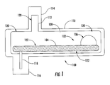
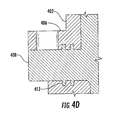
- A device, comprising:an electrical assembly having at least one electrical component;an inner shell comprising a first polymeric material disposed around the electrical assembly and in contact with the electrical assembly, the inner shell comprising a first mechanical strength; andan outer shell comprising a second polymeric material conformally disposed around the inner shell and in contact with the inner shell, the outer shell comprising a second mechanical strength greater than the first mechanical strength,wherein the electrical component comprises a first coefficient of thermal expansion (CTE) , the inner shell comprises a second CTE, and the outer shell comprises a third CTE, and wherein a difference between the first CTE and second CTE is less than a difference between the first CTE and third CTE.
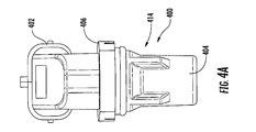
- The device of claim 1 wherein the electrical assembly has a first outer surface defining a first outer shape, the inner shell comprises a second outer surface defining a second outer shape different than the first outer shape; and wherein the outer shell comprises a third outer surface defining a third outer shape different than the first outer shape.
- The device of claim 1, wherein the inner shell comprises a thermoset material and the outer shell comprises a thermoplastic material.
- The device of claim 1, wherein the electrical assembly comprises a printed circuit board (PCB) and at least one electrical component disposed thereon.
- The device of claim 1, wherein the inner shell and outer shell are configured to operate over a temperature range of -50℃ to 150℃.
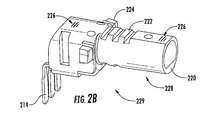
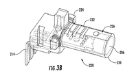
- The device of claim 2, wherein the second outer surface of the inner shell comprises a sealing rib assembly configured to increase sealing between the inner shell and outer shell by mechanically coupling to the outer shell.
- The device of claim 2, wherein the third outer shape is different than the second outer shape.
- The device of claim 1, wherein the inner shell comprises a post portion configured to couple to the outer shell.
- The device of claim 1, the outer shell comprising a second mechanical strength greater than the first mechanical strength.
- A method of forming an electrical device, comprising:providing an electrical assembly having at least one electrical component;forming an inner shell comprising a first polymeric material around the electrical assembly, the inner shell being in contact with the electrical assembly; andforming an outer shell comprising a second polymeric material around the inner shell and in contact with the inner shell,wherein the electrical assembly comprises a first coefficient of thermal expansion (CTE) , the inner shell comprises a second CTE, and the outer shell comprises a third CTE, and wherein a difference between the second CTE and first CTE is less than a difference between the third CTE and first CTE.
- The method of claim 10, wherein the forming the inner shell comprises:providing the electrical assembly in a first mold;dispensing a first liquid precursor of the inner shell into the first mold; andperforming a first injection molding process on the first liquid precursor and electrical component at a first temperature and a first pressure, wherein a singly encapsulated device is formed comprising the inner shell and electrical assembly.
- The method of claim 11, wherein the forming the outer shell comprises:providing the singly encapsulated device in a second mold;dispensing a second liquid precursor of the second polymeric material into the second mold; andperforming a second injection molding process on the singly encapsulated device at a second temperature and a second pressure greater than the first pressure.
- The method of claim 12, wherein the second temperature is higher than the first temperature.
- The method of claim 10, wherein the inner shell comprises a thermoset material, and wherein the outer shell comprises a thermoplastic material.
- The method of claim 12, wherein the first temperature is between 150℃ and 200℃ and the first pressure is between 20 kgf/cm2 and 100 kgf/cm2.
- The method of claim 12, wherein the second temperature is between 275 and 315℃ and the second pressure is between 700 kgf/cm2 and 1100 kgf/cm2.
- A sensor device, comprising:a printed circuit board;at least one sensor attached to the printed circuit board;an inner shell comprising a first polymeric material disposed around the printed circuit board and at least one electrical device, and in contact with the printed circuit board and at least one electrical device; andan outer shell comprising a second polymeric material disposed around the inner shell and in contact with the inner shell,wherein the printed circuit board comprises a first coefficient of thermal expansion (CTE) , the inner shell comprises a second CTE, and the outer shell comprises a third CTE, and wherein a difference between the first CTE and second CTE is less than a difference between the first CTE and third CTE.
- The device of claim 17, wherein the inner shell comprises a thermoset material and the outer shell comprises a thermoplastic material.
- The sensor device of claim 17, wherein the inner shell and outer shell are configured to operate over a temperature range of -50℃ to 150℃.
- The sensor device of claim 17, wherein the inner shell comprises:a sealing rib assembly configured to increase sealing between the inner shell and outer shell by mechanically coupling to the outer shell; anda post portion configured to couple to the outer shell.
Priority Applications (6)
| Application Number | Priority Date | Filing Date | Title |
|---|---|---|---|
| JP2017553073A JP6533594B2 (en) | 2015-04-10 | 2015-04-10 | Encapsulated electrical device and method of manufacture |
| CN201580078408.3A CN107532926B (en) | 2015-04-10 | 2015-04-10 | Packaged electrical device and method of manufacturing the same |
| US15/565,234 US10362692B2 (en) | 2015-04-10 | 2015-04-10 | Encapsulated electrical device and method of fabrication |
| KR1020177028076A KR102076961B1 (en) | 2015-04-10 | 2015-04-10 | Encapsulated Electrical Device and Manufacturing Method |
| EP15888174.8A EP3280979A4 (en) | 2015-04-10 | 2015-04-10 | Encapsulated electrical device and method of fabrication |
| PCT/CN2015/076260 WO2016161617A1 (en) | 2015-04-10 | 2015-04-10 | Encapsulated electrical device and method of fabrication |
Applications Claiming Priority (1)
| Application Number | Priority Date | Filing Date | Title |
|---|---|---|---|
| PCT/CN2015/076260 WO2016161617A1 (en) | 2015-04-10 | 2015-04-10 | Encapsulated electrical device and method of fabrication |
Publications (1)
| Publication Number | Publication Date |
|---|---|
| WO2016161617A1 true WO2016161617A1 (en) | 2016-10-13 |
Family
ID=57073026
Family Applications (1)
| Application Number | Title | Priority Date | Filing Date |
|---|---|---|---|
| PCT/CN2015/076260 WO2016161617A1 (en) | 2015-04-10 | 2015-04-10 | Encapsulated electrical device and method of fabrication |
Country Status (6)
| Country | Link |
|---|---|
| US (1) | US10362692B2 (en) |
| EP (1) | EP3280979A4 (en) |
| JP (1) | JP6533594B2 (en) |
| KR (1) | KR102076961B1 (en) |
| CN (1) | CN107532926B (en) |
| WO (1) | WO2016161617A1 (en) |
Families Citing this family (1)
| Publication number | Priority date | Publication date | Assignee | Title |
|---|---|---|---|---|
| US11395414B1 (en) * | 2020-04-09 | 2022-07-19 | General Atomics | Method to manufacture potted electronic assemblies for extreme mechanical and thermal environments |
Citations (11)
| Publication number | Priority date | Publication date | Assignee | Title |
|---|---|---|---|---|
| US6034421A (en) * | 1996-12-09 | 2000-03-07 | Denso Corporation | Semiconductor device including molded IC fixed to casing |
| US6307749B1 (en) | 2000-10-23 | 2001-10-23 | Delphi Technologies, Inc. | Overmolded electronic module with underfilled surface-mount components |
| CN1508516A (en) * | 2002-12-18 | 2004-06-30 | ��ʽ�����װ | Sensor with resin moulded casing and its producing method |
| US20060054901A1 (en) | 2004-09-16 | 2006-03-16 | Sharp Kabushiki Kaisha | Optical semiconductor device, method for fabricating the same, lead frame and electronic equipment |
| US20060125497A1 (en) | 2004-12-13 | 2006-06-15 | Richard Bond | Sanitary probe seal |
| US20060272150A1 (en) | 2003-07-03 | 2006-12-07 | Syuuji Eguchi | Module and method for fabricating the same |
| US20070139044A1 (en) | 2005-12-20 | 2007-06-21 | Honeywell International | Thermoplastic overmolding for small package turbocharger speed sensor |
| US20090004557A1 (en) | 2007-06-26 | 2009-01-01 | Nokia Corporation | Protecting a functional component and a protected functional component |
| US20110229702A1 (en) | 2005-10-18 | 2011-09-22 | Finisar Corporation | Reducing thermal expansion effects in semiconductor packages |
| DE102014212720A1 (en) * | 2013-07-01 | 2015-01-08 | Continental Teves Ag & Co. Ohg | Sensor with sealing coating |
| US20150092360A1 (en) | 2013-10-01 | 2015-04-02 | Nike, Inc. | Battery overmolding |
Family Cites Families (19)
| Publication number | Priority date | Publication date | Assignee | Title |
|---|---|---|---|---|
| JPH04307760A (en) | 1991-04-04 | 1992-10-29 | Mitsubishi Electric Corp | Resin-sealed semiconductor device |
| JP3316449B2 (en) * | 1997-07-03 | 2002-08-19 | 三洋電機株式会社 | Hybrid integrated circuit device and method of manufacturing the same |
| JP4585828B2 (en) * | 2004-10-06 | 2010-11-24 | 日立オートモティブシステムズ株式会社 | Control device and manufacturing method thereof |
| US7589401B2 (en) | 2006-08-09 | 2009-09-15 | Sri Hermetics Inc. | Lightweight, hermetically sealed package having auxiliary, selectively contoured, low mass, pseudo wall insert for surface-mounting and dissipating heat from electronic circuit components |
| US7819004B2 (en) * | 2006-09-27 | 2010-10-26 | Tk Holdings, Inc. | Vehicle sensor |
| CN101231933A (en) | 2007-01-25 | 2008-07-30 | 台达电子工业股份有限公司 | Cold cathode light tube |
| JP4518127B2 (en) * | 2007-10-01 | 2010-08-04 | 株式会社デンソー | Electronic circuit device manufacturing method and electronic circuit device |
| US7739791B2 (en) * | 2007-10-26 | 2010-06-22 | Delphi Technologies, Inc. | Method of producing an overmolded electronic module with a flexible circuit pigtail |
| CN201149495Y (en) | 2008-01-04 | 2008-11-12 | 潘劲松 | Sensing device for measuring relative humiture |
| CN101307773B (en) | 2008-05-26 | 2010-09-08 | 北京航空航天大学 | Aviation electronic oil fuel pump sealing method |
| JP5038273B2 (en) * | 2008-09-17 | 2012-10-03 | 三菱電機株式会社 | Resin molded semiconductor sensor and manufacturing method |
| US8234034B2 (en) * | 2009-06-26 | 2012-07-31 | Autoliv Asp, Inc. | Enhanced electronic assembly |
| US8578770B2 (en) * | 2010-11-02 | 2013-11-12 | Cantolino Industries, Inc. | Encapsulated liquid level sensor device |
| KR101449271B1 (en) * | 2013-04-19 | 2014-10-08 | 현대오트론 주식회사 | Electronic control apparatus for vehicle using overmolding and manufacturing method thereof |
| CN203375991U (en) | 2013-07-29 | 2014-01-01 | 杭州瑞利声电技术公司 | Combined sound pressure and hydraulic pressure sensor |
| CN103529311B (en) | 2013-09-30 | 2015-09-30 | 清华大学 | A kind of hydrophobic double seal optical electric field sensor being applicable to high humidity atmosphere |
| JP6373390B2 (en) * | 2013-10-10 | 2018-08-15 | インテル・コーポレーション | Use of materials to improve structural rigidity, reduce size, improve safety, and improve thermal performance and fast charging in small form factor devices |
| US9284981B2 (en) * | 2014-05-15 | 2016-03-15 | GM Global Technology Operations LLC | Expansion reduction of metal component assemblies using composites |
| EP3203818A4 (en) * | 2014-09-29 | 2018-04-25 | NGK Insulators, Ltd. | Sensor node package |
-
2015
- 2015-04-10 KR KR1020177028076A patent/KR102076961B1/en active IP Right Grant
- 2015-04-10 JP JP2017553073A patent/JP6533594B2/en active Active
- 2015-04-10 EP EP15888174.8A patent/EP3280979A4/en not_active Withdrawn
- 2015-04-10 CN CN201580078408.3A patent/CN107532926B/en active Active
- 2015-04-10 WO PCT/CN2015/076260 patent/WO2016161617A1/en active Application Filing
- 2015-04-10 US US15/565,234 patent/US10362692B2/en active Active
Patent Citations (12)
| Publication number | Priority date | Publication date | Assignee | Title |
|---|---|---|---|---|
| US6034421A (en) * | 1996-12-09 | 2000-03-07 | Denso Corporation | Semiconductor device including molded IC fixed to casing |
| US6307749B1 (en) | 2000-10-23 | 2001-10-23 | Delphi Technologies, Inc. | Overmolded electronic module with underfilled surface-mount components |
| CN1508516A (en) * | 2002-12-18 | 2004-06-30 | ��ʽ�����װ | Sensor with resin moulded casing and its producing method |
| US20060272150A1 (en) | 2003-07-03 | 2006-12-07 | Syuuji Eguchi | Module and method for fabricating the same |
| US20060054901A1 (en) | 2004-09-16 | 2006-03-16 | Sharp Kabushiki Kaisha | Optical semiconductor device, method for fabricating the same, lead frame and electronic equipment |
| US20060125497A1 (en) | 2004-12-13 | 2006-06-15 | Richard Bond | Sanitary probe seal |
| US7279910B2 (en) * | 2004-12-13 | 2007-10-09 | Anderson Instruments Co., Inc. | Sanitary probe seal |
| US20110229702A1 (en) | 2005-10-18 | 2011-09-22 | Finisar Corporation | Reducing thermal expansion effects in semiconductor packages |
| US20070139044A1 (en) | 2005-12-20 | 2007-06-21 | Honeywell International | Thermoplastic overmolding for small package turbocharger speed sensor |
| US20090004557A1 (en) | 2007-06-26 | 2009-01-01 | Nokia Corporation | Protecting a functional component and a protected functional component |
| DE102014212720A1 (en) * | 2013-07-01 | 2015-01-08 | Continental Teves Ag & Co. Ohg | Sensor with sealing coating |
| US20150092360A1 (en) | 2013-10-01 | 2015-04-02 | Nike, Inc. | Battery overmolding |
Non-Patent Citations (1)
| Title |
|---|
| See also references of EP3280979A4 |
Also Published As
| Publication number | Publication date |
|---|---|
| CN107532926B (en) | 2021-03-30 |
| KR102076961B1 (en) | 2020-02-13 |
| CN107532926A (en) | 2018-01-02 |
| JP2018512592A (en) | 2018-05-17 |
| EP3280979A4 (en) | 2018-12-05 |
| JP6533594B2 (en) | 2019-06-19 |
| US10362692B2 (en) | 2019-07-23 |
| US20180084657A1 (en) | 2018-03-22 |
| KR20170135852A (en) | 2017-12-08 |
| EP3280979A1 (en) | 2018-02-14 |
Similar Documents
| Publication | Publication Date | Title |
|---|---|---|
| US10349540B2 (en) | Mechatronic component and method for the production thereof | |
| US6320128B1 (en) | Environmentally-sealed electronic assembly and method of making same | |
| JP5038271B2 (en) | Electrical and electronic control device and manufacturing method thereof | |
| JP2013239660A5 (en) | ||
| JP7078003B2 (en) | Connector device | |
| US10362692B2 (en) | Encapsulated electrical device and method of fabrication | |
| US20080124987A1 (en) | Overmolded electronic assembly | |
| JP2009147014A (en) | Resin sealed type electronic control unit and sealing molding method thereof | |
| US20120043116A1 (en) | Interconnection Structure Of Interposer With Low CTE And Packaging Component Having The Same | |
| US7390551B2 (en) | System and method for encapsulation and protection of components | |
| JP6003897B2 (en) | Hollow sealing structure | |
| KR20140030889A (en) | Semiconductor chip package and manufacturing method thereof | |
| CN105675165A (en) | Temperature sensor and Method for manufacturing the same | |
| US7667978B2 (en) | Electronic package encapsulating electronic components therein | |
| US20230309237A1 (en) | Packaging structure, lens module, and electronic device | |
| JP2000133665A (en) | Method for sealing printed wiring board mounted with electronic component | |
| JP2008028017A (en) | Resin sealed semiconductor device | |
| US6506328B1 (en) | Process for producing an electronic component | |
| US10950563B2 (en) | Chip packages and methods for forming the same | |
| US9165794B1 (en) | Partial glob-top encapsulation technique | |
| CN111755874A (en) | Connector device | |
| US20050122697A1 (en) | Enhancement of underfill physical properties by the addition of a thermotropic cellulose | |
| WO2012019774A1 (en) | Fibre reinforced insulation material for embedded vacuum interrupters | |
| KR101179196B1 (en) | Wire Type Electronic Device Encapsulated by Transparent Material | |
| CN117043907A (en) | Electronic assembly with improved protection concept |
Legal Events
| Date | Code | Title | Description |
|---|---|---|---|
| 121 | Ep: the epo has been informed by wipo that ep was designated in this application |
Ref document number: 15888174 Country of ref document: EP Kind code of ref document: A1 |
|
| REEP | Request for entry into the european phase |
Ref document number: 2015888174 Country of ref document: EP |
|
| ENP | Entry into the national phase |
Ref document number: 20177028076 Country of ref document: KR Kind code of ref document: A |
|
| WWE | Wipo information: entry into national phase |
Ref document number: 15565234 Country of ref document: US |
|
| ENP | Entry into the national phase |
Ref document number: 2017553073 Country of ref document: JP Kind code of ref document: A |
|
| NENP | Non-entry into the national phase |
Ref country code: DE |