WO2016158641A1 - アンテナ装置、伝送モジュール、電子機器および伝送システム - Google Patents
アンテナ装置、伝送モジュール、電子機器および伝送システム Download PDFInfo
- Publication number
- WO2016158641A1 WO2016158641A1 PCT/JP2016/059309 JP2016059309W WO2016158641A1 WO 2016158641 A1 WO2016158641 A1 WO 2016158641A1 JP 2016059309 W JP2016059309 W JP 2016059309W WO 2016158641 A1 WO2016158641 A1 WO 2016158641A1
- Authority
- WO
- WIPO (PCT)
- Prior art keywords
- coil
- magnetic layer
- antenna device
- antenna
- disposed
- Prior art date
- Legal status (The legal status is an assumption and is not a legal conclusion. Google has not performed a legal analysis and makes no representation as to the accuracy of the status listed.)
- Ceased
Links
Images








Classifications
-
- G—PHYSICS
- G06—COMPUTING OR CALCULATING; COUNTING
- G06K—GRAPHICAL DATA READING; PRESENTATION OF DATA; RECORD CARRIERS; HANDLING RECORD CARRIERS
- G06K19/00—Record carriers for use with machines and with at least a part designed to carry digital markings
- G06K19/06—Record carriers for use with machines and with at least a part designed to carry digital markings characterised by the kind of the digital marking, e.g. shape, nature, code
- G06K19/067—Record carriers with conductive marks, printed circuits or semiconductor circuit elements, e.g. credit or identity cards also with resonating or responding marks without active components
- G06K19/07—Record carriers with conductive marks, printed circuits or semiconductor circuit elements, e.g. credit or identity cards also with resonating or responding marks without active components with integrated circuit chips
- G06K19/077—Constructional details, e.g. mounting of circuits in the carrier
-
- H—ELECTRICITY
- H01—ELECTRIC ELEMENTS
- H01Q—ANTENNAS, i.e. RADIO AERIALS
- H01Q21/00—Antenna arrays or systems
- H01Q21/30—Combinations of separate antenna units operating in different wavebands and connected to a common feeder system
-
- H—ELECTRICITY
- H01—ELECTRIC ELEMENTS
- H01Q—ANTENNAS, i.e. RADIO AERIALS
- H01Q7/00—Loop antennas with a substantially uniform current distribution around the loop and having a directional radiation pattern in a plane perpendicular to the plane of the loop
- H01Q7/06—Loop antennas with a substantially uniform current distribution around the loop and having a directional radiation pattern in a plane perpendicular to the plane of the loop with core of ferromagnetic material
-
- H—ELECTRICITY
- H02—GENERATION; CONVERSION OR DISTRIBUTION OF ELECTRIC POWER
- H02J—ELECTRIC POWER NETWORKS; CIRCUIT ARRANGEMENTS OR SYSTEMS FOR SUPPLYING OR DISTRIBUTING ELECTRIC POWER; SYSTEMS FOR STORING ELECTRIC ENERGY
- H02J50/00—Circuit arrangements or systems for wireless supply or distribution of electric power
- H02J50/10—Circuit arrangements or systems for wireless supply or distribution of electric power using inductive coupling
Definitions
- the present invention relates to an antenna device having two types of coils and a magnetic layer, and a transmission module, an electronic device, and a transmission system provided with such an antenna device.
- mobile terminal devices such as mobile phone terminals including smartphones and tablet PCs (Personal Computers), NFC (Near Field Communication), that is, devices equipped with a non-contact (wireless) communication function are widely used.
- NFC Near Field Communication
- portable terminal devices those equipped with a non-contact power feeding function for charging a battery by transmitting (transmitting) electric power in a non-contact (wireless) manner are being used.
- Patent Document 1 discloses an antenna device in which a plurality of types of coils such as a non-contact communication coil and a non-contact power supply coil coexist in a housing.
- such an antenna device is generally required to improve its characteristics (transmission characteristics, etc.). Therefore, a proposal of a method for improving such characteristics is desired.
- an antenna device capable of improving characteristics, and a transmission module, an electronic device, and a transmission system provided with such an antenna device.
- a first antenna device includes a first coil, a first magnetic layer disposed so as to overlap at least a part of the first coil, and a first coil
- a second coil disposed on the outside and a second magnetic layer disposed so as to overlap at least a part of the second coil are provided.
- the cross-sectional area per turn of the winding in the first coil is larger than the cross-sectional area per turn of the winding in the second coil.
- the second coil and the second magnetic layer have a gap between them.
- a first transmission module includes an antenna device and an electronic component.
- the antenna device includes a first coil, a first magnetic layer disposed so as to overlap at least a part of the first coil, a second coil disposed outside the first coil, And a second magnetic layer disposed so as to overlap at least a part of the second coil.
- the cross-sectional area per turn of the winding in the first coil is larger than the cross-sectional area per turn of the winding in the second coil.
- the second coil and the second magnetic layer have a gap between them.
- a first electronic device includes a transmission module having an antenna device and an electronic component.
- the antenna device includes a first coil, a first magnetic layer disposed so as to overlap at least a part of the first coil, a second coil disposed outside the first coil, And a second magnetic layer disposed so as to overlap at least a part of the second coil.
- the cross-sectional area per turn of the winding in the first coil is larger than the cross-sectional area per turn of the winding in the second coil.
- the second coil and the second magnetic layer have a gap between them.
- a first transmission system includes a first transmission module, and a second transmission module that transmits power and signals to the first transmission module in a contactless manner. It is equipped with.
- Each of the first and second transmission modules includes an antenna device and an electronic component.
- the antenna device in at least one of the first and second transmission modules includes a first coil, a first magnetic layer disposed so as to overlap at least a part of the first coil, It has the 2nd coil arrange
- the cross-sectional area per turn of the winding in the first coil is larger than the cross-sectional area per turn of the winding in the second coil.
- the second coil and the second magnetic layer have a gap between them.
- a second antenna device includes a first coil, a first magnetic layer disposed so as to overlap at least part of the first coil, and a first coil
- a second coil disposed on the outside and a second magnetic layer disposed so as to overlap at least a part of the second coil are provided.
- the cross-sectional area per turn of the winding in the first coil is larger than the cross-sectional area per turn of the winding in the second coil.
- the inner edge of the second magnetic layer is disposed inside the inner edge of the second coil, and the outer edge of the second magnetic layer is It arrange
- a second transmission module includes an antenna device and an electronic component.
- the antenna device includes a first coil, a first magnetic layer disposed so as to overlap at least a part of the first coil, a second coil disposed outside the first coil, And a second magnetic layer disposed so as to overlap at least a part of the second coil.
- the cross-sectional area per turn of the winding in the first coil is larger than the cross-sectional area per turn of the winding in the second coil.
- the inner edge of the second magnetic layer is disposed inside the inner edge of the second coil, and the outer edge of the second magnetic layer is It arrange
- a second electronic device includes a transmission module having an antenna device and an electronic component.
- the antenna device includes a first coil, a first magnetic layer disposed so as to overlap at least a part of the first coil, a second coil disposed outside the first coil, And a second magnetic layer disposed so as to overlap at least a part of the second coil.
- the cross-sectional area per turn of the winding in the first coil is larger than the cross-sectional area per turn of the winding in the second coil.
- the inner edge of the second magnetic layer is disposed inside the inner edge of the second coil, and the outer edge of the second magnetic layer is It arrange
- a second transmission system includes a first transmission module, a second transmission module that transmits power and signals to the first transmission module in a contactless manner, and It is equipped with.
- Each of the first and second transmission modules includes an antenna device and an electronic component.
- the antenna device in at least one of the first and second transmission modules includes a first coil, a first magnetic layer disposed so as to overlap at least a part of the first coil, It has the 2nd coil arrange
- the cross-sectional area per turn of the winding in the first coil is larger than the cross-sectional area per turn of the winding in the second coil.
- the inner edge of the second magnetic layer is disposed inside the inner edge of the second coil, and the outer edge of the second magnetic layer is It arrange
- first magnetic layer “second magnetic layer”, “winding”, “electronic component”, “antenna device” and “(first and second) transmission module” (of The “number” is a concept including both one and plural (any two or more).
- the antenna device According to the antenna device, the transmission module, the electronic device, and the transmission system according to the embodiment of the present invention, it is possible to improve the characteristics.
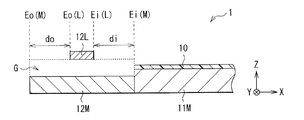
- FIG. 2 is a schematic diagram illustrating an enlarged cross-sectional configuration example in the vicinity of an end of the antenna device illustrated in FIG. 1.
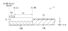
- FIG. 5 is a schematic diagram illustrating an enlarged view of another cross-sectional configuration example near the end of the antenna device illustrated in FIG. 1.
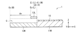
- FIG. 5 is a schematic diagram illustrating an enlarged view of another cross-sectional configuration example near the end of the antenna device illustrated in FIG. 1.
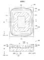
- 5 is a schematic diagram illustrating a planar configuration and a cross-sectional configuration of an antenna device according to Comparative Example 1.
- FIG. 6 is a schematic diagram illustrating a planar configuration and a cross-sectional configuration of an antenna device according to Comparative Example 2.
- FIG. FIG. 10 is a diagram illustrating values of parameters according to Experimental Examples 1-1 to 1-12. It is a figure showing the correspondence of the gap
- FIG. 10 is a diagram illustrating values of parameters according to Experimental Examples 2-1 to 2-5. It is a figure showing the correspondence of distance do shown in Drawing 6A, and standardized Q value. It is a schematic diagram showing the example of a plane structure of the antenna device which concerns on the modification 1 of this invention. It is a schematic diagram showing the example of a plane structure of the antenna device which concerns on the modification 2 of this invention.
- Embodiment Example of basic configuration of antenna device having gap between coil and magnetic layer for communication
- Modified example Modified example 1 (an example in which a communication magnetic layer is superimposed on three sides of a communication coil)
- Modified examples 2 to 4 an example in which the magnetic layer is also superimposed on a part of the remaining one side in modified example 1)
- Modification 5 example in which a nonmagnetic dielectric layer is inserted in the gap
- Modification 6 example in which a coil for non-contact power feeding is embedded in a magnetic resin layer
- Modified example 7 example in which the magnetic layer for communication is also disposed below the magnetic layer for non-contact power feeding
- Application examples Application examples 1 to 4: Application examples to transmission modules, electronic devices, and transmission systems) 4).
- Other variations Application examples 1 to 4: Application examples to transmission modules, electronic devices, and transmission systems
- FIG. 1 schematically shows an antenna device (antenna device 1) according to an embodiment of the present invention.
- FIG. 1A illustrates a planar configuration example (XY top surface configuration example) of the antenna device 1
- FIG. 1B illustrates a cross-sectional configuration example of the antenna device 1
- FIG. 2 illustrates a ZX cross-sectional configuration example along the line II-II in FIG.
- the antenna device 1 has both a non-contact power feeding function (non-contact power transmission function) and a non-contact communication function (non-contact signal transmission function), which will be described later, and is a so-called “combo type” antenna. Device. As shown in FIG. 1A and FIG. 1B, the antenna device 1 includes two types of antenna units (the antenna unit 11 and the antenna unit 12).
- the antenna unit 11 is an antenna unit having a non-contact power feeding function (an antenna unit for non-contact power feeding).
- the frequency band of the antenna unit 11 is, for example, about 100 kHz to 200 kHz (kilohertz band) in the case of the Qi standard that is an international standard established by WPC (Wireless Power Consortium).
- the antenna unit 11 may be used for either power transmission or power reception during such non-contact power feeding.
- the antenna unit 11 includes a coil 11L and a magnetic layer 11M.
- the antenna unit 11 corresponds to a specific example of “first antenna unit” in the present invention.
- the coil 11L corresponds to a specific example of “first coil” in the present invention
- the magnetic layer 11M corresponds to a specific example of “first magnetic layer” in the present invention.
- the coil 11L has one or a plurality of windings w1 having a predetermined cross-sectional area S1 wound on the magnetic layer 11M described later a predetermined number of times (number of turns). It is a coil.
- the coil 11L includes a pair of long sides extending along the Y-axis direction and a pair of short sides extending along the X-axis direction, as shown in FIG. A substantially rectangular winding structure is included.
- the ends of the winding w1 in the coil 11L are each pulled out of the antenna device 1 in the -Y-axis direction in this example.
- the length ranges of the long side portion and the short side portion are not particularly limited.
- the winding w1 in the coil 11L is made of a conductive material such as Cu (copper) or Al (aluminum), for example.
- the magnetic layer 11M is a magnetic layer disposed so as to overlap at least a part of the coil 11L.
- the entire coil 11L (the entire region) is overlapped. Has been placed.
- the magnetic layer 11M is disposed below the coil 11L with the adhesive 10 (adhesive layer) interposed therebetween.
- the coil 11L and the magnetic layer 11M are bonded to each other by the adhesive 10.
- an adhesive 10 for example, a general inorganic adhesive or organic adhesive, a double-sided tape, or the like is used.
- the magnetic layer 11M has a rectangular planar shape having a major axis (Y-axis direction) and a minor axis (X-axis direction), as shown in FIGS. It has a sheet shape having a predetermined thickness (length in the Z-axis direction).
- the length of the major axis of the magnetic layer 11M is, for example, longer than the length of the long side portions LLp and LLn of the coil 12L described later.
- the length of the short axis in the magnetic layer 11M is, for example, approximately longer than the length of the short side portion in the coil 11L.
- Such a magnetic layer 11M is made of a magnetic material having a magnetic permeability suitable for non-contact power feeding using a coil 11L described later, and includes, for example, various metal magnetic materials.
- metal magnetic bodies include amorphous magnetic bodies and crystalline magnetic bodies (eg, Sendust (Fe (iron) -Si (silicon) -Al alloy), Fe-Si alloys, Fe-Ni alloys, etc.)). Is mentioned.
- the thickness d1 (see FIG. 1B) of the entire antenna unit 11 (in this example, a structure in which the coil 11L, the magnetic layer 11M, and the adhesive 10 are stacked) will be described in detail later. It is desirable to satisfy a predetermined magnitude relationship with the thickness d2 of the entire antenna unit 12 to be described.
- the antenna unit 12 is an antenna unit (non-contact communication antenna unit) having a non-contact communication function such as NFC, and the frequency band thereof is, for example, about 13.56 MHz (megahertz band) in the NFC standard.
- the antenna unit 12 may be used for transmission, reception, and transmission / reception in such non-contact communication.
- the antenna unit 12 includes a coil 12L and a magnetic layer 12M.
- the antenna unit 12 corresponds to a specific example of “second antenna unit” in the present invention.
- the coil 12L corresponds to a specific example of the “second coil” in the present invention
- the magnetic layer 12M corresponds to a specific example of the “second magnetic layer” in the present invention.
- the coil 12L has one or a plurality of windings w2 having a predetermined cross-sectional area S2 wound around the magnetic layer 12M described later a predetermined number of times (number of turns). It is a coil.
- the coil 12L includes a pair of long side portions LLp and LLn extending along the Y-axis direction and a pair of short sides extending along the X-axis direction, as shown in FIG. It has a substantially rectangular winding structure including the parts LSp and LSn.
- the coil 12L has a winding structure similar to that of the coil 11L described above, and is arranged concentrically around the coil 11L on the outer side (outer peripheral side) of the coil 11L.
- the end of the winding w2 in the coil 12L is also similar to the end of the winding w1 described above, in this example, toward the ⁇ Y axis direction, the antenna device 1 It is designed to be pulled out outside.
- the lengths (length in the Y-axis direction) of the long side portions LLp and LLn in the coil 12L are longer than the length of the long side portion (the length in the Y-axis direction) in the coil 11L described above. If it is, those ranges are not specifically limited. Also, the lengths (length in the X-axis direction) of the short side portions LSp and LSn are also longer than the length of the short side portion (length in the X-axis direction) of the coil 11L described above. For example, those ranges are not particularly limited.
- the winding w2 in the coil 12L is made of a conductive material such as Cu or Al, for example, like the winding w1 described above.
- the (effective) cross-sectional area S2 per turn in the winding w2 is, for example, as follows. That is, as schematically shown in FIG. 1B, the cross-sectional area S1 per turn in the winding w1 is larger than the cross-sectional area S2 per turn in the winding w2. (Cross-sectional area S1> cross-sectional area S2). This is because the non-contact power supply coil 11L requires a larger amount of power than the non-contact communication coil 12L.
- the magnetic layer 12M is a magnetic layer disposed so as to overlap at least a part of the coil 12L.
- the magnetic layer 12M is disposed below the coil 12L so as to overlap a part of the coil 12L.
- the magnetic layer 12M is disposed so as to overlap two sides (each of the pair of long side portions LLp and LLn) of the coil 12L.
- the remaining two sides (each of the pair of short sides LSp and LSn) in the coil 12L, that is, the non-overlapping region of the magnetic layer 12M in the coil 12L are as shown in FIG.
- the magnetic layer 11M in the antenna unit 11 is arranged so as to overlap.
- the magnetic layer 12M has a rectangular planar shape having a long axis (Y-axis direction) and a short axis (X-axis direction) in this example. It has a sheet shape having a predetermined thickness (length in the Z-axis direction).
- Such a sheet-like magnetic layer 12M is disposed outside the magnetic layer 11M (on the outer edge sides at both ends along the X-axis direction).
- the antenna unit 12 including such a magnetic layer 12M is disposed outside the antenna unit 11 including the magnetic layer 11M.
- the length of the major axis in the magnetic layer 12M is, for example, approximately longer than the length of the long side portions LLp and LLn in the coil 12L.
- the length of the short axis in the magnetic layer 12M is, for example, approximately larger than the winding width of the winding w2 in the coil 12L.
- Such a magnetic layer 12M is configured using a magnetic material having a magnetic permeability suitable for non-contact communication using a coil 12L described later, and includes, for example, various oxide magnetic materials.
- a magnetic oxide include Ni (nickel) -Zn (zinc) based ferrite and Mn (manganese) -Zn based ferrite.
- the coil 12L and the magnetic layer 12M have a gap G (a space having a predetermined interlayer distance) between them. ing.
- a gap G is realized, for example, by using a predetermined spacer (for example, double-sided tape) to secure the coil 12L and the magnetic layer 12M with a predetermined interval therebetween.
- the length of the gap G (the length in the Z-axis direction) is, for example, a magnitude relationship between the thickness d1 of the entire antenna portion 11 and the thickness d2 of the entire antenna portion 12 (thickness d2 ⁇ thickness d1) described below. It is set within the range that satisfies.
- the thickness d2 (see FIG. 1B) of the entire antenna unit 12 is, for example, as follows. That is, as shown in FIG. 1B, in this example, the thickness d2 of the antenna portion 12 is smaller than the thickness d1 of the antenna portion 11 described above (thickness d2 ⁇ thickness d1). In other words, the antenna unit 12 has a structure that is thinner than the antenna unit 11.
- the periphery of the overlapping region of the coil 12L and the magnetic layer 12M (this) In the example, it is as follows in the vicinity of both end portions along the X-axis direction in the antenna device 1.
- the cross-sectional configuration example shown in FIG. 2A is more preferable around the overlapping region than the cross-sectional configuration example shown in FIGS. 2B and 2C.
- the inner edge Ei (M) of the magnetic layer 12M is disposed on the inner side (by the distance di) than the inner edge Ei (L) of the coil 12L.
- the outer edge Eo (M) of the magnetic layer 12M is arranged outside the outer edge Eo (L) of the coil 12L (by the distance do).
- the inner edge Ei (M) of the magnetic layer 12M is disposed on the inner side (by the distance di) than the inner edge Ei (L) of the coil 12L.
- the outer edge Eo (M) of the magnetic layer 12M is disposed outside the outer edge Eo (L) of the coil 12L (by the distance do).
- a non-contact power transmission operation (feed operation) is performed between the coil 11L and the non-contact power supply coil (not shown) in the other antenna device. Is called. That is, a non-contact power transmission operation or power reception operation is performed.
- a non-contact signal transmission operation (communication operation) is performed between the antenna 12 and the coil for non-contact communication in the other antenna device. That is, non-contact transmission operation, reception operation, or transmission / reception operation is performed.
- FIG. 3 schematically illustrates the antenna device (antenna device 100) according to Comparative Example 1. Specifically, FIG. 3A illustrates a planar configuration example (XY top surface configuration example) of the antenna device 100, and FIG. 3B illustrates a cross-sectional configuration example of the antenna device 100 ( FIG. 4 illustrates a ZX cross-sectional configuration example taken along line III-III in FIG.
- the antenna device 100 of Comparative Example 1 is an antenna device having both a non-contact power feeding function and a non-contact communication function, and includes two types of coils 11L and 12L and one type of magnetic layer 100M. And. That is, the antenna device 100 corresponds to the antenna device 1 in which the magnetic layer 100M is provided instead of the magnetic layers 11M and 12M, and other configurations are basically the same.
- the magnetic layer 100M is a magnetic layer common to the two types of coils 11L and 12L. As shown in FIG. 3B, the magnetic layer 100M is disposed below the coils 11L and 12L via the adhesive 10 so as to overlap the entire area of the coils 11L and 12L.
- the magnetic layer 100M is a magnetic layer common to the coils 11L and 12L, the following problems occur. That is, since the frequency band to be used is different between contactless power supply (kilohertz band) and contactless communication (megahertz band), this magnetic layer 100M is suitable for both contactless power supply and contactless communication. A magnetic material (magnetic material) (having a magnetic permeability) cannot be used. For this reason, in Comparative Example 1, the characteristics of the antenna device 100 as a whole are degraded.
- the power transmission characteristic in the coil 11L is lowered, while a magnetic material suitable for non-contact power feeding is used in the magnetic layer 100M. In this case, the communication characteristics in the coil 12L are deteriorated.
- FIG. 4 schematically shows an antenna device (antenna device 200) according to Comparative Example 2.
- FIG. 4A illustrates a planar configuration example (XY top surface configuration example) of the antenna device 200
- FIG. 4B illustrates a cross-sectional configuration example of the antenna device 200
- FIG. 5 illustrates a ZX cross-sectional configuration example along line IV-IV in FIG.
- the antenna device 200 of the comparative example 2 is also an antenna device having both a non-contact power feeding function and a non-contact communication function, as with the antenna device 1, and includes an antenna unit 201 and an antenna unit 202. That is, the antenna device 200 corresponds to the antenna device 1 in which the antenna units 201 and 202 are provided instead of the antenna units 11 and 12, and the other configurations are basically the same.
- the antenna unit 201 is an antenna unit having a non-contact power feeding function (an antenna unit for non-contact power feeding), and includes a coil 11L and a magnetic layer 11M.
- the antenna unit 202 is an antenna unit (non-contact communication antenna unit) having a non-contact communication function, and includes a coil 12L and a magnetic layer 12M.
- the magnetic layer 11M is disposed on the entire surface of the antenna device 200 so as to overlap the entire region of the coil 12L.
- the antenna unit 202 has a magnetic layer 12 ⁇ / b> M disposed on the magnetic layer 11 ⁇ / b> M so as to overlap the entire four sides (long side portions LLp and LLn and short side portions LSp and LSn) of the coil 12 ⁇ / b> L.
- a coil 12L is disposed immediately above the magnetic layer 12M (no gap G is provided).
- the communication characteristics (for example, the antenna unit 202) are caused by the proximity effect between the coil 12L and the magnetic layer 12M. Q value) will decrease. This can be said to be particularly susceptible to such a proximity effect because the frequency band during non-contact communication in the antenna unit 202 is high (megahertz band).
- the thickness d202 of the antenna portion 202 is larger than the thickness d201 of the antenna portion 201 as shown in FIG. (Thickness d202> thickness d201). Therefore, the antenna unit 202 is not thinner than the antenna unit 201, and it is difficult to reduce the thickness of the antenna device 200 as a whole.
- the following can be said because there is a large demand for thinning. That is, it is not preferable to increase the thickness of the entire antenna device 200 by adding the antenna unit 202 for non-contact communication in order to function as a so-called “combo type” antenna device.
- the antenna device 1 according to the present embodiment is as follows, unlike the first and second comparative examples.
- the antenna unit 11 includes a magnetic layer 11M using a magnetic material having a magnetic permeability suitable for non-contact power feeding. It is included.
- the antenna unit 12 includes a magnetic layer 12M using a magnetic material having a magnetic permeability suitable for non-contact communication. Therefore, appropriate magnetic layers 11M and 12M are individually provided in the antenna units 11 and 12, and unlike the first comparative example, the characteristic degradation of the antenna device 1 as a whole is avoided. That is, in this antenna device 1, compared with the antenna device 100 of the comparative example 1, the power transmission characteristics and the communication characteristics are improved.
- the thickness d2 of the antenna unit 12 is smaller than the thickness d1 of the antenna unit 11 (thickness d2 ⁇ thickness d1). Therefore, in the present embodiment, unlike Comparative Example 2, obstruction of the overall thickness reduction of the antenna device 1 due to the non-contact communication antenna unit 12 is avoided. As a result, the antenna device 1 can be made thinner as a whole as compared with the antenna device 200 of the comparative example 2.
- the inner edge Ei (M) of the magnetic layer 12M is disposed inside the inner edge Ei (L) of the coil 12L in the periphery of the overlapping region of the coil 12M and the magnetic layer 12L.
- the outer edge Eo (M) of the magnetic layer 12M is arranged outside the outer edge Eo (L) of the coil 12L, the following occurs.
- the antenna device 1 is compared with the case where the outer edge Eo (M) of the magnetic layer 12M and the outer edge Eo (L) of the coil 12L are arranged to coincide with each other.
- Adverse effects from outside a metal member disposed in the periphery; for example, a housing
- the communication characteristics of the antenna unit 12 are improved.
- it is easy to receive such a bad influence from the outside so that a frequency band is high, it can be said that the merit which suppresses such a bad influence is large in the high frequency band to use (megahertz band).
- the antenna for non-contact power feeding is compared with the case where the inner edge Ei (M) of the magnetic layer 12M and the inner edge Ei (L) of the coil 12L are arranged to coincide with each other.
- the adverse effect from the magnetic layer 11M in the part 11 is suppressed, and this also contributes to the improvement of the communication characteristics in the antenna part 12.
- the magnetic layer 12M is disposed so as to overlap the long side portions LLp and LLn in the coil 12L.
- the magnetic layer 12M is arrange
- the gap G is provided between the coil 12L and the magnetic layer 12M in the antenna unit 12, the influence of the proximity effect between the coil 12L and the magnetic layer 12M can be suppressed. it can. Therefore, the communication characteristics (for example, Q value) in the antenna unit 12 are improved, and the characteristics (transmission characteristics and the like) of the antenna device 1 as a whole can be improved.
- the inner edge Ei (M) of the magnetic layer 12M is arranged on the inner side of the inner edge Ei (L) of the coil 12L, and the outer edge Eo (M) of the magnetic layer 12M is more than the outer edge Eo (L) of the coil 12L.
- the communication characteristics (for example, Q value) in the antenna unit 12 are further improved, and the characteristics of the antenna device 1 as a whole can be further improved.
- the antenna device 1 as a whole can be thinned.
- the antenna device since the so-called “combo type” antenna device as in the present embodiment is generally often mounted on a mobile terminal device, the antenna device needs to be thin (downsized). Therefore, it is required to maintain (improve) characteristics (transmission efficiency, communication performance, etc.) above a certain level. In the antenna device 1 according to the present embodiment, it is possible to contribute to both the improvement of the characteristics and the reduction in thickness.
- the arrangement structure of the present embodiment does not cause an adverse effect (side effect) on the original performance (communication performance) of the antenna device 1.
- FIG. 5A is a table summarizing the values of the parameters according to Experimental Examples 1-1 to 1-12.
- the value of the gap G (length in the Z-axis direction) between the coil 12L and the magnetic layer 12M is set to 0 ⁇ m (Experimental Example 1-1) to 300 ⁇ m (Experimental Example 1-12).
- the correspondence between the measured Q value and the normalized Q value (relative value based on the Q value in Experimental Example 1-1) when changing by 25 ⁇ m is shown. Yes.
- the Q value was measured using Agilent 4294A (manufactured by Keysight Technologies Inc.) under the condition that the frequency band at the antenna unit 12 was 13.56 MHz. This also applies to Experimental Examples 2-1 to 2-5 described later.
- the detailed configurations of the antenna unit 11 (the coil 11L and the magnetic layer 11M) and the antenna unit 12 (the coil 12L and the magnetic layer 12M) in each of the experimental examples 1-1 to 1-12 are as follows. is there. -Number of turns of coil 11L: 16 turns (two in parallel) -Inner diameter of coil 11L: 18 mm x 23 mm -Wire diameter of the coil 11L: 0.22mm -Size of magnetic layer 11M (metal magnetic sheet): (52mm x 35mm) x 0.3mm (thickness) -Number of turns of coil 12L: 3 turns (winding width: 1mm) -Inner diameter of coil 12L: 43mm x 48mm -Wire diameter of coil 12L: 0.10mm -Size of magnetic layer 12M (Ni-Zn ferrite magnetic sheet): (52mm x 5mm) x 0.2mm (thickness) ⁇ Spacer to secure each numerical gap G: Use double-sided tape with a thickness of
- FIG. 5B is a graph showing the correspondence between the gap G and the standardized Q value for each of the experimental examples 1-1 to 1-12 shown in FIG. 5A.
- the Q value gradually increases (almost monotonously increases).
- the Q value hardly changes and is saturated.
- the influence of the proximity effect between the coil 12L and the magnetic layer 12M can be suppressed (current distribution in the coil 12L).
- the Q value at the antenna unit 12 increased. This is presumably because the proximity effect appears prominently because the frequency band at the antenna unit 12 is as high as 13.56 MHz.
- the frequency band is relatively low at about 200 KHz at the maximum, so it can be said that it is hardly affected by the proximity effect.
- FIG. 6A is a table summarizing the values of the parameters according to Experimental Examples 2-1 to 2-5. Specifically, in FIG. 6A, the value of the distance do (the distance from the outer edge Eo (M) of the magnetic layer 12M to the outer edge Eo (L) of the coil 12L) is 0 mm (Experimental Example 2-1) to The measured Q value and the normalized Q value (relative values based on the Q value in Experimental Example 2-3) when changing by 1 mm in the range of 4 mm (Experimental Example 2-5) ).
- the detailed configurations of the antenna unit 11 (the coil 11L and the magnetic layer 11M) and the antenna unit 12 (the coil 12L and the magnetic layer 12M) in each of the experimental examples 2-1 to 2-5 are as follows.
- FIG. 6B is a graph showing the correspondence between the distance do and the standardized Q value for each of the experimental examples 2-1 to 2-5 shown in FIG. 6A.
- the inner edge Ei (M) of the magnetic layer 12M is disposed on the inner side of the inner edge Ei (L) of the coil 12L, and the outer edge Eo (M) of the magnetic layer 12M is the outer edge Eo (L) of the coil 12L.
- the Q value in the antenna unit 12 is increased by being arranged outside the).
- FIG. 7 schematically illustrates a planar configuration example (XY top surface configuration example) of the antenna device (antenna device 1A) according to the first modification.
- a cross-sectional configuration example (ZX cross-sectional configuration example) in the antenna device 1A is basically the same as the cross-sectional configuration example in the antenna device 1 shown in FIG.
- the antenna device 1A of the present modification is an antenna device having both a non-contact power feeding function and a non-contact communication function, as with the antenna device 1 of the embodiment, and includes an antenna unit 11A and an antenna unit 12A. That is, the antenna device 1A corresponds to the antenna device 1 in which the antenna units 11A and 12A are provided instead of the antenna units 11 and 12, and other configurations are basically the same.
- the antenna unit 11A is an antenna unit having a non-contact power feeding function (an antenna unit for non-contact power feeding), and includes a coil 11L and a magnetic layer 11M.
- the antenna unit 12A is an antenna unit having a non-contact communication function (an antenna unit for non-contact communication), and includes a coil 12L and a magnetic layer 12M.
- the magnetic layer 12M is provided on the three sides of the coil 12L (in addition to the pair of long side portions LLp and LLn). It arrange
- the magnetic layer 12M is arranged so as to overlap with the short side portion LSp in addition to the long side portions LLp and LLn, so that the inductance in the coil 12L can be further increased, and Compared to the form, it is possible to further improve the communication characteristics in the antenna unit 12A.
- FIG. 8 illustrates a planar configuration example of the antenna device 1B according to Modification Example 2
- FIG. 9 illustrates a planar configuration example of the antenna device 1C according to Modification Example 3
- FIG. 2 shows a planar configuration example of the antenna device 1D according to FIG.
- the cross-sectional configuration example (ZX cross-sectional configuration example) in these antenna devices 1B to 1D is basically the same as the cross-sectional configuration example in the antenna device 1 shown in FIG. Omitted.
- antenna devices 1B to 1D are antenna devices having both a non-contact power feeding function and a non-contact communication function, as with the antenna device 1 of the embodiment. Further, in each of the antenna devices 1B to 1D, similarly to the antenna device 1A of the first modification, the magnetic layer 12M is disposed so as to overlap each of the long side portions LLp, LLn and the short side portion LSp.
- the magnetic layer 12M is further arranged so as to overlap with a part of the other short side portion LSn of the pair of short side portions LSp and LSn. Then, the winding w1 in at least the coil 11L among the windings w1 and w2 in the coils 11L and 12L is connected to the antenna device 1B via the remaining region (the non-arrangement region of the magnetic layer 12M) in the short side LSn. It is designed to be pulled out to 1D.
- Modification 2 Specifically, the antenna device 1B of Modification 2 shown in FIG. 8 corresponds to the antenna device 1 in which the antenna units 11B and 12B are provided instead of the antenna units 11 and 12, and the other configuration is basically the same. Are similar.
- the antenna unit 11B is an antenna unit having a non-contact power feeding function (an antenna unit for non-contact power feeding), and includes a coil 11L and a magnetic layer 11M.
- the antenna unit 12B is an antenna unit having a non-contact communication function (antenna unit for non-contact communication), and includes a coil 12L and a magnetic layer 12M.
- the short side portion LSn in addition to the long side portions LLp and LLn and the short side portion LSp, a part of the short side portion LSn (in this example, the vicinity of the central region in the short side portion LSn)
- the magnetic layer 12M is disposed so as to overlap with the other region.
- the ends of the windings w1 and w2 of the coils 11L and 12L are drawn out of the antenna device 1B from the vicinity of the central region of the short side LSn (the non-arrangement region of the magnetic layer 12M). ing.
- the antenna device 1C of the third modification shown in FIG. 9 corresponds to the antenna device 1 in which the antenna units 11B and 12C are provided instead of the antenna units 11 and 12, and other configurations are basically the same. ing.
- the antenna unit 12C is an antenna unit having a non-contact communication function (an antenna unit for non-contact communication), and includes a coil 12L and a magnetic layer 12M.
- each end of the winding w1 of the coil 11L is connected to the other region from the one region.
- Each end of the winding w2 of the coil 12L is pulled out from the region to the outside of the antenna device 1C.
- Modification 4 The antenna device 1D of Modification 4 shown in FIG. 10 corresponds to the antenna device 1 in which the antenna units 11B and 12D are provided instead of the antenna units 11 and 12, and other configurations are basically the same. ing.
- the antenna unit 12D is an antenna unit having a non-contact communication function (an antenna unit for non-contact communication), and includes a coil 12L and a magnetic layer 12M.
- the magnetic layer 12M is disposed so as to overlap with the region.
- the non-arrangement region of the magnetic layer 12M located between the three divided regions in the short side portion LSn, one end portion of the winding w1 of the coil 11L from one region is The other end of the winding w1 in the coil 11L is drawn out of the antenna device 1D.
- each end of the winding w2 in the coil 12L is drawn out of the antenna device 1D via the arrangement region (on the magnetic layer 12M) of the magnetic layer 12M.
- the magnetic layer 12M It may be drawn to the outside through the arrangement region (on the magnetic layer 12M).
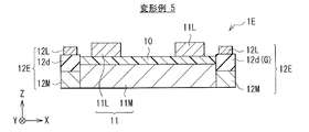
- FIGS. 11 to 13 schematically show cross-sectional configuration examples (ZX cross-sectional configuration examples) of antenna devices (antenna devices 1E to 1G) according to Modifications 5 to 7.
- the antenna device 1E of Modification 5 shown in FIG. 11 corresponds to the antenna device 1 in which the antenna unit 12E is provided instead of the antenna unit 12, and the other configurations are basically the same.
- This antenna portion 12E is the antenna portion 12 shown in FIG. 1B, and further has a nonmagnetic dielectric layer 12d inserted in the gap G between the coil 12L and the magnetic layer 12M.
- the other configurations are basically the same.
- the nonmagnetic dielectric layer 12d is made of a nonmagnetic and nonconductive material (nonmagnetic dielectric) such as PET (polyethylene terephthalate) resin, acrylic resin, or epoxy resin. Further, the thickness of the nonmagnetic dielectric layer 12d is, for example, the thickness d1 of the entire antenna portion 11 and the thickness d2 of the entire antenna portion 12E, similar to the length of the gap G (the length in the Z-axis direction) described above. It is set within a range satisfying the magnitude relationship (thickness d2 ⁇ thickness d1).
- the nonmagnetic dielectric layer 12d is inserted in the gap G.
- a layer made of a magnetic material or a conductive material is inserted in the gap G.
- the antenna device 1F of Modification 6 shown in FIG. 12 corresponds to the antenna device 1 in which the antenna unit 11F is provided instead of the antenna unit 11, and the other configurations are basically the same.
- This antenna portion 11F corresponds to the antenna portion 11 shown in FIG. 1B in which a magnetic resin layer 11R is further provided, and other configurations are basically the same.
- the magnetic resin layer 11R is arranged so that at least a part of the coil 11L (in this example, the side surface and the lower surface of the coil 11L) is embedded (embedded). In other words, the magnetic resin layer 11R is disposed so as to cover the side surface and the lower surface of the coil 11L.
- a magnetic resin layer 11R is made of, for example, a resin or the like (magnetic resin) containing magnetic powder such as amorphous magnetic powder or Sendust.
- the magnetic resin layer 11R is disposed so that at least a part of the coil 11L is embedded, the following effects can also be obtained. That is, first, it is possible to increase the inductance of the coil 11L and improve the power transmission characteristics in the antenna unit 11F. Further, the heat dissipation from the coil 11L can be improved. Furthermore, the adhesiveness with the magnetic layer 11M can be improved, and the adhesive 10 becomes unnecessary.
- the antenna device 1G of the modified example 7 shown in FIG. 13 corresponds to the antenna device 1 in which the antenna units 11G and 12G are provided instead of the antenna units 11 and 12, and other configurations are basically the same. ing.
- the antenna unit 11G is an antenna unit having a non-contact power feeding function (an antenna unit for non-contact power feeding), and includes a coil 11L and a magnetic layer 11M.
- the antenna unit 12G is an antenna unit (non-contact communication antenna unit) having a non-contact communication function, and includes a coil 12L and a magnetic layer 12M.
- the magnetic layer 12M is disposed so as to overlap below the antenna portion 11G (entire region).
- the coil 12L is arrange
- the thickness of the antenna unit 12G is smaller than the thickness of the antenna unit 11G, as in the above-described embodiment and the like. Therefore, also in this modified example, the antenna device 1G as a whole can be thinned.
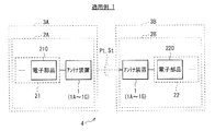
- FIGS. 14A to 14D schematically show block configuration examples of transmission systems (transmission systems 4, 4A to 4C) according to application examples 1 to 4 of the present invention.
- FIG. 14A illustrates a block configuration example of the transmission system 4 according to Application Example 1
- FIG. 14B illustrates a block configuration example of the transmission system 4A according to Application Example 2.
- 14C illustrates a block configuration example of the transmission system 4B according to Application Example 3
- FIG. 14D illustrates a block configuration example of the transmission system 4C according to Application Example 4.
- the transmission system 4 of Application Example 1 illustrated in FIG. 14A includes one or a plurality (one in this example) of electronic devices 3A and one electronic device 3B.
- the transmission system 4 can transmit the electric power Pt and the signal St from the electronic device 3A to the electronic device 3B in a non-contact manner (using the above-described electromagnetic induction method, magnetic field resonance method, etc.). System.
- the electronic device 3A is, for example, an electronic device such as a non-contact charging tray with a non-contact communication function, and has one or a plurality of (in this example, one) transmission module 2A.
- the transmission module 2A has a function (a contactless power feeding function and a contactless communication function described above) that sends power Pt and a signal St in a contactless manner to a transmission module 2B in an electronic device 3B described later ( Transmission module on the sending side).
- the transmission module 2A includes one or more (one in this example) antenna device 1 described in the above embodiment (or any one of the antenna devices 1A to 1G described in the first to seventh modifications), one or And a functional unit 21 including a plurality of electronic components 210.
- the transmission module 2A corresponds to a specific example of “second transmission module” in the present invention.
- the functional unit 21 is a part for exercising each function (such as a non-contact power feeding function using the coil 11L and a non-contact communication function using the coil 12L) in the antenna device 1 (1A to 1G) in the transmission module 2A ( Circuit part).
- the electronic component 210 included in the functional unit 21 is a variety of electronic components that constitute such a circuit unit, such as various capacitors (capacitance elements), transistors, power supply units, voltage or current detection units, and control units. IC (Integrated (Circuit) etc.
- the electronic device 3B is, for example, an electronic device (mainly a portable electronic device) including a rechargeable battery (battery) such as a mobile phone or a digital camera, and one or a plurality (in this example, one) of transmission modules. 2B.
- the transmission module 2B is a module (reception-side transmission module) having a function of receiving the electric power Pt and the signal St transmitted from the transmission module 2A in the electronic device 3A in a contactless manner.
- the transmission module 2B includes one or a plurality (one in this example) of the antenna device 1 described in the above embodiment (or any one of the antenna devices 1A to 1G described in the modified examples 1 to 7), 1 or And a functional unit 22 including a plurality of electronic components 220.
- the transmission module 2B corresponds to a specific example of “first transmission module” in the present invention.
- the function unit 22 is a part (for example, a non-contact power supply function using the coil 11L and a non-contact communication function using the coil 12L) in the antenna device 1 (1A to 1G) in the transmission module 2B. Circuit part).
- the electronic component 220 included in the functional unit 22 is various electronic components that constitute such a circuit unit, and includes, for example, various capacitors (capacitance elements), transistors, rectifying elements, smoothing elements, control ICs, and the like. .
- the transmission system 4A of the application example 2 illustrated in FIG. 14B includes one or a plurality (one in this example) of electronic devices 3A and a plurality (two in this example) of electronic devices 3B1 and 3B2.
- the transmission system 4A is a system that can transmit the electric power Pt and the signal St from the electronic device 3A to each of the electronic devices 3B1 and 3B2 in a non-contact manner, for example, by time division or simultaneous parallel.
- the transmission system 4 of the application example 1 is a so-called “1: 1” system (a system in which the sending side and the receiving side have a 1: 1 configuration), whereas the transmission system 4A of the application example.
- Each of the electronic devices 3B1 and 3B2 has the same configuration as the above-described electronic device 3B, and has one or a plurality of (in this example, one) transmission module 2B.
- the transmission system 4B of the application example 3 illustrated in FIG. 14C includes one or more (one in this example) electronic device 3A and one electronic device 303B.
- the transmission system 4B is a system that can transmit the power Pt and the signal St from the electronic device 3A to the electronic device 303B in a non-contact manner.
- the electronic device 303B has one or a plurality of (in this example, one) transmission module 302B. Similar to the transmission module 2B, the transmission module 302B is a module (reception-side transmission module) having a function of receiving the power Pt and the signal St transmitted in a non-contact manner from the transmission module 2A in the electronic device 3A. .
- the transmission module 302 ⁇ / b> B includes a conventional antenna device 300 (for example, the antenna devices 100 and 200 of Comparative Examples 1 and 2 described above) and a functional unit 22 including one or more electronic components 220. That is, the transmission module 302B corresponds to the transmission module 2B in which the antenna device 300 having the conventional configuration is provided instead of the antenna device 1 (1A to 1G), and the other configurations are basically the same.
- the transmission system 4C of the application example 4 illustrated in FIG. 14D includes one or more (one in this example) electronic device 303A and one electronic device 3B.
- the transmission system 4C is a system that can transmit the power Pt and the signal St from the electronic device 303A to the electronic device 3B in a non-contact manner.
- the electronic device 303A has one or a plurality of (in this example, one) transmission module 302A. Similar to the transmission module 2A, the transmission module 302A is a module (a transmission module on the sending side) having a function of sending the power Pt and the signal St without contact to the transmission module 2B in the electronic device 3B. .
- the transmission module 302 ⁇ / b> A includes the antenna device 300 (for example, the antenna devices 100 and 200) having the above-described conventional configuration and the functional unit 21 including one or more electronic components 210. That is, the transmission module 302A corresponds to the transmission module 2A in which the antenna device 300 having the conventional configuration is provided instead of the antenna device 1 (1A to 1G), and other configurations are basically the same.
- the antenna device 1 (1A to 1G) of the above-described embodiment or the like is provided only on one side of the transmission module on the sending side and the transmission module on the receiving side. You may do it.
- the antenna device 1 (1A to 4A) is provided on at least one of the transmission module on the transmission side and the transmission module on the reception side. 1G) is provided. Accordingly, in a system that transmits the power Pt and the signal St in a non-contact manner, it is possible to improve the transmission characteristics of the power Pt and the signal St, and to realize a reduction in size and thickness of the entire system. It becomes possible.
- each member described in the above embodiment is not limited, and other shapes, arrangement positions, materials, etc. may be used.
- each magnetic layer may be disposed so as to overlap with at least a part of the coil, and does not necessarily overlap with the entire region of the coil.
- the present invention is not limited to this. That is, for example, in a configuration in which such a gap G is not provided, the inner edge Ei (M) of the magnetic layer 12M is disposed on the inner side of the inner edge Ei (L) of the coil 12L, and the magnetic The outer edge Eo (M) of the layer 12M may be arranged outside the outer edge Eo (L) of the coil 12L.
- the thickness of the antenna part for non-contact communication is smaller than the thickness of the antenna part for non-contact power feeding has been described as an example, but the present invention is not limited thereto. . That is, for example, the thickness of the non-contact communication antenna unit may be equal to or greater than the thickness of the non-contact power supply antenna unit.
- transmission modules, electronic devices, and transmission systems have been described as application examples of the antenna device according to the present invention.
- the present invention is not limited thereto, and the antenna device according to the present invention You may make it apply to an apparatus, a module, and a system.
Landscapes
- Engineering & Computer Science (AREA)
- Computer Hardware Design (AREA)
- Microelectronics & Electronic Packaging (AREA)
- Physics & Mathematics (AREA)
- General Physics & Mathematics (AREA)
- Theoretical Computer Science (AREA)
- Computer Networks & Wireless Communication (AREA)
- Power Engineering (AREA)
- Details Of Aerials (AREA)
- Variable-Direction Aerials And Aerial Arrays (AREA)
Abstract
アンテナ装置は、第1のコイルと、この第1のコイルの少なくとも一部分に重畳するように配置された第1の磁性層と、第1のコイルの外側に配置された第2のコイルと、この第2のコイルの少なくとも一部分に重畳するように配置された第2の磁性層とを備えている。第1のコイルにおける巻線の1ターン当りの断面積は、第2のコイルにおける巻線の1ターン当りの断面積よりも大きくなっている。第2のコイルおよび第2の磁性層は、それらの間に間隙を有している。
Description
本発明は、2種類のコイルおよび磁性層を有するアンテナ装置、ならびに、そのようなアンテナ装置を備えた伝送モジュール、電子機器および伝送システムに関する。
スマートフォンを含む携帯電話端末やタブレットPC(Personal Computer)等の携帯端末機器では、NFC(Near Field Communication)、すなわち、非接触(無線)通信機能を搭載したものが普及している。このような携帯端末機器ではまた、非接触(ワイヤレス)で電力を伝達(伝送)することによって電池への充電を行う、非接触給電機能を搭載したものが用いられつつある。
加えて、これら2つの機能の双方を搭載した携帯端末機器も普及し始めている。具体的には、そのような携帯端末機器では、非接触通信用のアンテナ部と非接触給電用のアンテナ部との双方が内蔵されるようになっている。また、例えば特許文献1には、非接触通信用コイルおよび非接触給電用コイルなどの複数種類のコイルが筐体内に共存されるようにしたアンテナ装置が開示されている。
ところで、このようなアンテナ装置では一般に、その特性(伝送特性等)を向上させることが求められている。したがって、そのような特性を向上させる手法の提案が望まれる。
したがって、特性を向上させることが可能なアンテナ装置、ならびに、そのようなアンテナ装置を備えた伝送モジュール、電子機器および伝送システムを提供することが望ましい。
本発明の一実施の形態に係る第1のアンテナ装置は、第1のコイルと、この第1のコイルの少なくとも一部分に重畳するように配置された第1の磁性層と、第1のコイルの外側に配置された第2のコイルと、この第2のコイルの少なくとも一部分に重畳するように配置された第2の磁性層とを備えたものである。第1のコイルにおける巻線の1ターン当りの断面積は、第2のコイルにおける巻線の1ターン当りの断面積よりも大きくなっている。第2のコイルおよび第2の磁性層は、それらの間に間隙を有している。
本発明の一実施の形態に係る第1の伝送モジュールは、アンテナ装置と電子部品とを備えたものである。上記アンテナ装置は、第1のコイルと、この第1のコイルの少なくとも一部分に重畳するように配置された第1の磁性層と、第1のコイルの外側に配置された第2のコイルと、この第2のコイルの少なくとも一部分に重畳するように配置された第2の磁性層とを有している。第1のコイルにおける巻線の1ターン当りの断面積は、第2のコイルにおける巻線の1ターン当りの断面積よりも大きくなっている。第2のコイルおよび第2の磁性層は、それらの間に間隙を有している。
本発明の一実施の形態に係る第1の電子機器は、アンテナ装置と電子部品とを有する伝送モジュールを備えたものである。上記アンテナ装置は、第1のコイルと、この第1のコイルの少なくとも一部分に重畳するように配置された第1の磁性層と、第1のコイルの外側に配置された第2のコイルと、この第2のコイルの少なくとも一部分に重畳するように配置された第2の磁性層とを有している。第1のコイルにおける巻線の1ターン当りの断面積は、第2のコイルにおける巻線の1ターン当りの断面積よりも大きくなっている。第2のコイルおよび第2の磁性層は、それらの間に間隙を有している。
本発明の一実施の形態に係る第1の伝送システムは、第1の伝送モジュールと、この第1の伝送モジュールに対して、電力および信号をそれぞれ非接触にて伝送する第2の伝送モジュールとを備えたものである。第1および第2の伝送モジュールはそれぞれ、アンテナ装置と電子部品とを有している。第1および第2の伝送モジュールのうちの少なくとも一方におけるアンテナ装置は、第1のコイルと、この第1のコイルの少なくとも一部分に重畳するように配置された第1の磁性層と、第1のコイルの外側に配置された第2のコイルと、この第2のコイルの少なくとも一部分に重畳するように配置された第2の磁性層とを有している。第1のコイルにおける巻線の1ターン当りの断面積は、第2のコイルにおける巻線の1ターン当りの断面積よりも大きくなっている。第2のコイルおよび第2の磁性層は、それらの間に間隙を有している。
本発明の一実施の形態に係る第2のアンテナ装置は、第1のコイルと、この第1のコイルの少なくとも一部分に重畳するように配置された第1の磁性層と、第1のコイルの外側に配置された第2のコイルと、この第2のコイルの少なくとも一部分に重畳するように配置された第2の磁性層とを備えたものである。第1のコイルにおける巻線の1ターン当りの断面積は、第2のコイルにおける巻線の1ターン当りの断面積よりも大きくなっている。第2のコイルと第2の磁性層との重畳領域の周辺において、第2の磁性層の内縁が第2のコイルの内縁よりも内側に配置されていると共に、第2の磁性層の外縁が第2のコイルの外縁よりも外側に配置されている。
本発明の一実施の形態に係る第2の伝送モジュールは、アンテナ装置と電子部品とを備えたものである。上記アンテナ装置は、第1のコイルと、この第1のコイルの少なくとも一部分に重畳するように配置された第1の磁性層と、第1のコイルの外側に配置された第2のコイルと、この第2のコイルの少なくとも一部分に重畳するように配置された第2の磁性層とを有している。第1のコイルにおける巻線の1ターン当りの断面積は、第2のコイルにおける巻線の1ターン当りの断面積よりも大きくなっている。第2のコイルと第2の磁性層との重畳領域の周辺において、第2の磁性層の内縁が第2のコイルの内縁よりも内側に配置されていると共に、第2の磁性層の外縁が第2のコイルの外縁よりも外側に配置されている。
本発明の一実施の形態に係る第2の電子機器は、アンテナ装置と電子部品とを有する伝送モジュールを備えたものである。上記アンテナ装置は、第1のコイルと、この第1のコイルの少なくとも一部分に重畳するように配置された第1の磁性層と、第1のコイルの外側に配置された第2のコイルと、この第2のコイルの少なくとも一部分に重畳するように配置された第2の磁性層とを有している。第1のコイルにおける巻線の1ターン当りの断面積は、第2のコイルにおける巻線の1ターン当りの断面積よりも大きくなっている。第2のコイルと第2の磁性層との重畳領域の周辺において、第2の磁性層の内縁が第2のコイルの内縁よりも内側に配置されていると共に、第2の磁性層の外縁が第2のコイルの外縁よりも外側に配置されている。
本発明の一実施の形態に係る第2の伝送システムは、第1の伝送モジュールと、この第1の伝送モジュールに対して、電力および信号をそれぞれ非接触にて伝送する第2の伝送モジュールとを備えたものである。第1および第2の伝送モジュールはそれぞれ、アンテナ装置と電子部品とを有している。第1および第2の伝送モジュールのうちの少なくとも一方におけるアンテナ装置は、第1のコイルと、この第1のコイルの少なくとも一部分に重畳するように配置された第1の磁性層と、第1のコイルの外側に配置された第2のコイルと、この第2のコイルの少なくとも一部分に重畳するように配置された第2の磁性層とを有している。第1のコイルにおける巻線の1ターン当りの断面積は、第2のコイルにおける巻線の1ターン当りの断面積よりも大きくなっている。第2のコイルと第2の磁性層との重畳領域の周辺において、第2の磁性層の内縁が第2のコイルの内縁よりも内側に配置されていると共に、第2の磁性層の外縁が第2のコイルの外縁よりも外側に配置されている。
なお、本発明における「第1の磁性層」、「第2の磁性層」、「巻線」、「電子部品」、「アンテナ装置」および「(第1および第2の)伝送モジュール」(の個数)はそれぞれ、1または複数(2以上のいずれか)のいずれをも含む概念のものである。
本発明の一実施の形態に係るアンテナ装置、伝送モジュール、電子機器および伝送システムによれば、特性を向上させることが可能となる。
以下、本発明の実施の形態について、図面を参照して詳細に説明する。なお、説明は以下の順序で行う。
1.実施の形態(通信用のコイル・磁性層間に間隙を有するアンテナ装置の基本構成例)
2.変形例
変形例1(通信用のコイルの3辺に通信用の磁性層が重畳されている例)
変形例2~4(変形例1において残り1辺の一部にも磁性層が重畳されている例)
変形例5(間隙に非磁性誘電体層が挿設されている例)
変形例6(非接触給電用のコイルが磁性樹脂層に埋設されている例)
変形例7(通信用の磁性層が非接触給電用の磁性層の下部にも配置されている例)
3.適用例(適用例1~4:伝送モジュール、電子機器および伝送システムへの適用例)
4.その他の変形例
1.実施の形態(通信用のコイル・磁性層間に間隙を有するアンテナ装置の基本構成例)
2.変形例
変形例1(通信用のコイルの3辺に通信用の磁性層が重畳されている例)
変形例2~4(変形例1において残り1辺の一部にも磁性層が重畳されている例)
変形例5(間隙に非磁性誘電体層が挿設されている例)
変形例6(非接触給電用のコイルが磁性樹脂層に埋設されている例)
変形例7(通信用の磁性層が非接触給電用の磁性層の下部にも配置されている例)
3.適用例(適用例1~4:伝送モジュール、電子機器および伝送システムへの適用例)
4.その他の変形例
<1.実施の形態>
[構成]
図1は、本発明の一実施の形態に係るアンテナ装置(アンテナ装置1)を模式的に表したものである。具体的には、図1(A)は、このアンテナ装置1の平面構成例(X-Y上面構成例)を表したものであり、図1(B)は、アンテナ装置1の断面構成例(図1(A)中のII-II線に沿ったZ-X断面構成例)を表したものである。なお、図1(A)の平面構成例においては、便宜上、後述する接着剤10の図示は省略されており、以降の他の平面構成例の図においても同様である。
[構成]
図1は、本発明の一実施の形態に係るアンテナ装置(アンテナ装置1)を模式的に表したものである。具体的には、図1(A)は、このアンテナ装置1の平面構成例(X-Y上面構成例)を表したものであり、図1(B)は、アンテナ装置1の断面構成例(図1(A)中のII-II線に沿ったZ-X断面構成例)を表したものである。なお、図1(A)の平面構成例においては、便宜上、後述する接着剤10の図示は省略されており、以降の他の平面構成例の図においても同様である。
このアンテナ装置1は、後述する非接触給電機能(非接触による電力の伝送機能)および非接触通信機能(非接触による信号の伝送機能)の双方を有しており、いわゆる「コンボタイプ」のアンテナ装置である。アンテナ装置1は、図1(A)および図1(B)に示したように、2種類のアンテナ部(アンテナ部11およびアンテナ部12)を備えている。
(アンテナ部11)
アンテナ部11は、非接触給電機能を有するアンテナ部(非接触給電用のアンテナ部)である。このアンテナ部11の周波数帯域は、例えば、WPC(Wireless Power Consortium)により策定された国際標準規格であるQi(チー)規格の場合、100kHz~200kHz程度(キロヘルツ帯域)となっている。なお、アンテナ部11は、そのような非接触給電の際の送電用および受電用のいずれとして使用されるものであってもよい。このアンテナ部11は、図1(A)および図1(B)に示したように、コイル11Lおよび磁性層11Mを有している。なお、アンテナ部11は、本発明における「第1のアンテナ部」の一具体例に対応する。また、コイル11Lは本発明における「第1のコイル」の一具体例に対応し、磁性層11Mは本発明における「第1の磁性層」の一具体例に対応する。
アンテナ部11は、非接触給電機能を有するアンテナ部(非接触給電用のアンテナ部)である。このアンテナ部11の周波数帯域は、例えば、WPC(Wireless Power Consortium)により策定された国際標準規格であるQi(チー)規格の場合、100kHz~200kHz程度(キロヘルツ帯域)となっている。なお、アンテナ部11は、そのような非接触給電の際の送電用および受電用のいずれとして使用されるものであってもよい。このアンテナ部11は、図1(A)および図1(B)に示したように、コイル11Lおよび磁性層11Mを有している。なお、アンテナ部11は、本発明における「第1のアンテナ部」の一具体例に対応する。また、コイル11Lは本発明における「第1のコイル」の一具体例に対応し、磁性層11Mは本発明における「第1の磁性層」の一具体例に対応する。
コイル11Lは、図1(B)に示したように、所定の断面積S1を有する1または複数の巻線w1が、後述する磁性層11M上で所定の回数(ターン数)だけ巻回されてなるコイルである。コイル11Lは、この例では図1(A)に示したように、Y軸方向に沿って延在する一対の長辺部と、X軸方向に沿って延在する一対の短辺部とを含む略矩形状の巻線構造を有している。なお、図1(A)に示したように、このコイル11Lにおける巻線w1の端部はそれぞれ、この例では-Y軸方向へ向かってアンテナ装置1の外部へ引き出されるようになっている。
このようなコイル11Lにおける上記長辺部の長さ(Y軸方向の長さ)については、上記短辺部の長さ(X軸方向の長さ)よりも長くなっているのであれば、これら長辺部および短辺部の長さの範囲はそれぞれ、特に限定されるものではない。また、このコイル11Lにおける巻線w1は、例えば、Cu(銅)やAl(アルミニウム)等の導電性材料により構成されている。
磁性層11Mは、コイル11Lの少なくとも一部分に重畳するように配置される磁性層であり、この例では図1(A)に示したように、コイル11Lの全体(全領域)を重畳するように配置されている。また、この磁性層11Mは、接着剤10(接着層)を介してコイル11Lの下方に配置されている。換言すると、コイル11Lと磁性層11Mとは、接着剤10によって互いに接着されている。なお、このような接着剤10としては、例えば、一般的な無機系接着剤もしくは有機系接着剤、または、両面テープ等が用いられるようになっている。
磁性層11Mはまた、図1(A)および図1(B)に示したように、この例では、長軸(Y軸方向)および短軸(X軸方向)を有する矩形状の平面形状を有していると共に、所定の厚み(Z軸方向の長さ)を有するシート状となっている。なお、磁性層11Mにおけるこの長軸の長さは、例えば、後述するコイル12Lにおける長辺部LLp,LLnの長さよりも長くなっている程度である。また、磁性層11Mにおける上記短軸の長さは、例えば、上記したコイル11Lにおける短辺部の長さよりも長くなっている程度である。
このような磁性層11Mは、後述するコイル11Lを用いた非接触給電に適した透磁率を有する磁性材料を用いて構成されており、例えば、各種の金属磁性体を含んで構成されている。そのような金属磁性体としては、例えば、アモルファス磁性体や結晶系磁性体(例えば、センダスト(Fe(鉄)-Si(ケイ素)-Al合金),Fe-Si合金,Fe-Ni合金等)などが挙げられる。
なお、このようなアンテナ部11全体(この例では、コイル11L、磁性層11Mおよび接着剤10が積層された構造)の厚みd1(図1(B)参照)は、詳細は後述するが、以下説明するアンテナ部12全体の厚みd2との間で、所定の大小関係を満たすようになっているのが望ましい。
(アンテナ部12)
アンテナ部12は、NFC等の非接触通信機能を有するアンテナ部(非接触通信用のアンテナ部)であり、その周波数帯域は、例えばNFC規格の場合、13.56MHz程度(メガヘルツ帯域)である。なお、アンテナ部12は、そのような非接触通信の際の送信用、受信用および送受信用のいずれとして使用されるものであってもよい。このアンテナ部12は、図1(A)および図1(B)に示したように、コイル12Lおよび磁性層12Mを有している。なお、アンテナ部12は、本発明における「第2のアンテナ部」の一具体例に対応する。また、コイル12Lは本発明における「第2のコイル」の一具体例に対応し、磁性層12Mは本発明における「第2の磁性層」の一具体例に対応する。
アンテナ部12は、NFC等の非接触通信機能を有するアンテナ部(非接触通信用のアンテナ部)であり、その周波数帯域は、例えばNFC規格の場合、13.56MHz程度(メガヘルツ帯域)である。なお、アンテナ部12は、そのような非接触通信の際の送信用、受信用および送受信用のいずれとして使用されるものであってもよい。このアンテナ部12は、図1(A)および図1(B)に示したように、コイル12Lおよび磁性層12Mを有している。なお、アンテナ部12は、本発明における「第2のアンテナ部」の一具体例に対応する。また、コイル12Lは本発明における「第2のコイル」の一具体例に対応し、磁性層12Mは本発明における「第2の磁性層」の一具体例に対応する。
コイル12Lは、図1(B)に示したように、所定の断面積S2を有する1または複数の巻線w2が、後述する磁性層12M上で所定の回数(ターン数)だけ巻回されてなるコイルである。コイル12Lは、この例では図1(A)に示したように、Y軸方向に沿って延在する一対の長辺部LLp,LLnと、X軸方向に沿って延在する一対の短辺部LSp,LSnとを含む略矩形状の巻線構造を有している。すなわち、コイル12Lは、前述したコイル11Lと同様の巻線構造を有しており、このコイル11Lの外側(外周側)においてコイル11Lを周回するように同心状に配置されている。なお、図1(A)に示したように、コイル12Lにおける巻線w2の端部もそれぞれ、前述した巻線w1の端部と同様に、この例では-Y軸方向へ向かってアンテナ装置1の外部へ引き出されるようになっている。
このようなコイル12Lにおける長辺部LLp,LLnの長さ(Y軸方向の長さ)についてはそれぞれ、前述したコイル11Lにおける長辺部の長さ(Y軸方向の長さ)よりも長くなっているのであれば、それらの範囲は特に限定されるものではない。また、短辺部LSp,LSnの長さ(X軸方向の長さ)についてもそれぞれ、前述したコイル11Lにおける短辺部の長さ(X軸方向の長さ)よりも長くなっているのであれば、それらの範囲は特に限定されるものではない。なお、このコイル12Lにおける巻線w2は、前述した巻線w1と同様に、例えば、CuやAl等の導電性材料により構成されている。
ここで、この巻線w2における1ターン当りの(実効的な)断面積S2は、例えば以下のようになっている。すなわち、図1(B)中に模式的に示したように、前述した巻線w1における1ターン当りの断面積S1のほうが、この巻線w2における1ターン当りの断面積S2よりも大きくなっている(断面積S1>断面積S2)。これは、非接触給電用のコイル11Lのほうが非接触通信用のコイル12Lよりも大きな電力を要することに起因している。
磁性層12Mは、コイル12Lの少なくとも一部分に重畳するように配置される磁性層である。この例では図1(A)および図1(B)に示したように、磁性層12Mは、コイル12Lの一部分を重畳するように、このコイル12Lの下方に配置されている。具体的には、磁性層12Mは、この例ではコイル12Lの2辺(一対の長辺部LLp,LLnの各々)に重畳するように配置されている。
なお、コイル12Lにおける残りの2辺(一対の短辺部LSp,LSnの各々)、すなわち、コイル12Lにおける磁性層12Mの非重畳領域には、この例では図1(A)に示したように、アンテナ部11における磁性層11Mが重畳するように配置されている。
磁性層12Mはまた、図1(A)および図1(B)に示したように、この例では、長軸(Y軸方向)および短軸(X軸方向)を有する矩形状の平面形状を有していると共に、所定の厚み(Z軸方向の長さ)を有するシート状となっている。そして、このようなシート状の磁性層12Mが、磁性層11Mの外側(X軸方向に沿った両端の外縁側)にそれぞれ配置されている。換言すると、このような磁性層12Mを含むアンテナ部12は、磁性層11Mを含むアンテナ部11の外側に配置されている。なお、磁性層12Mにおける上記長軸の長さは、例えば、上記したコイル12Lにおける長辺部LLp,LLnの長さよりも長くなっている程度程度である。また、磁性層12Mにおける上記短軸の長さは、例えば、このコイル12Lにおける巻線w2の巻幅よりも大きくなっている程度である。
このような磁性層12Mは、後述するコイル12Lを用いた非接触通信に適した透磁率を有する磁性材料を用いて構成されており、例えば、各種の酸化物磁性体を含んで構成されている。そのような酸化物磁性体としては、例えば、Ni(ニッケル)-Zn(亜鉛)系フェライトや、Mn(マンガン)-Zn系フェライト等が挙げられる。
ここで、このアンテナ部12では、図1(B)中に模式的に示したように、コイル12Lおよび磁性層12Mが、それらの間に間隙G(所定の層間距離を有する空間)を有している。このような間隙Gは、例えば、所定のスペーサ(例えば両面テープ等)を用いて、コイル12Lおよび磁性層12M同士を所定間隔を確保して固定することで実現されるようになっている。なお、この間隙Gの長さ(Z軸方向の長さ)は、例えば、以下説明する、アンテナ部11全体の厚みd1とアンテナ部12全体の厚みd2との大小関係(厚みd2<厚みd1)を満たす範囲内に設定されるようになっている。
また、アンテナ部12全体(この例では、間隙Gを介してコイル12Lおよび磁性層12Mが積層された構造)の厚みd2(図1(B)参照)は、例えば以下のようになっている。つまり、図1(B)に示したように、この例では、アンテナ部12における厚みd2が、前述したアンテナ部11の厚みd1よりも小さくなっている(厚みd2<厚みd1)。換言すると、このアンテナ部12は、アンテナ部11よりも薄型化された構造となっている。
ここで、例えば図2A~図2Cに模式的な断面図(Z-X断面図)で示したように、このアンテナ部12では、更に、コイル12Lと磁性層12Mとの重畳領域の周辺(この例では、アンテナ装置1におけるX軸方向に沿った両端部付近)において、以下のようになっている。
すなわち、この重畳領域の周辺では、図2Bおよび図2Cに示した断面構成例よりも、図2Aに示した断面構成例となっているほうが望ましい。具体的には、この図2Aに示した断面構成例では、磁性層12Mの内縁Ei(M)が、コイル12Lの内縁Ei(L)よりも(距離diの分だけ)内側に配置されている。また、磁性層12Mの外縁Eo(M)が、コイル12Lの外縁Eo(L)よりも(距離doの分だけ)外側に配置されている。
一方、図2Bに示した断面構成例では、磁性層12Mの内縁Ei(M)が、コイル12Lの内縁Ei(L)よりも(距離diの分だけ)内側に配置されているが、磁性層12Mの外縁Eo(M)とコイル12Lの外縁Eo(L)とが互いに一致するように配置されている(Eo(M)=Eo(L))。つまり、この例では、上記した距離do=0(ゼロ)となっている。
他方、図2Cに示した断面構成例では、磁性層12Mの外縁Eo(M)が、コイル12Lの外縁Eo(L)よりも(距離doの分だけ)外側に配置されているが、磁性層12Mの内縁Ei(M)とコイル12Lの内縁Ei(L)とが互いに一致するように配置されている(Ei(M)=Ei(L))。つまり、この例では、上記した距離di=0となっている。
[作用・効果]
(A.基本動作)
このアンテナ装置1では、外部の他のアンテナ装置(図示せず)との間で、磁界を用いた(電磁誘導方式や磁界共鳴方式等を利用した)非接触による電力および信号の伝送動作がそれぞれ行われる。
(A.基本動作)
このアンテナ装置1では、外部の他のアンテナ装置(図示せず)との間で、磁界を用いた(電磁誘導方式や磁界共鳴方式等を利用した)非接触による電力および信号の伝送動作がそれぞれ行われる。
具体的には、アンテナ部11では、コイル11Lを用いて、上記他のアンテナ装置における非接触給電用のコイル(図示せず)との間で、非接触による電力伝送動作(給電動作)が行われる。すなわち、非接触による送電動作あるいは受電動作がなされる。
一方、アンテナ部12では、コイル12Lを用いて、上記他のアンテナ装置における非接触通信用のコイルとの間で、非接触による信号伝送動作(通信動作)が行われる。すなわち、非接触による送信動作、受信動作あるいは送受信動作がなされる。
(B.アンテナ装置1における作用)
続いて、このようなアンテナ装置1における作用について、比較例(比較例1,2)と比較しつつ詳細に説明する。
続いて、このようなアンテナ装置1における作用について、比較例(比較例1,2)と比較しつつ詳細に説明する。
(B-1.比較例1)
図3は、比較例1に係るアンテナ装置(アンテナ装置100)を模式的に表したものである。具体的には、図3(A)は、このアンテナ装置100の平面構成例(X-Y上面構成例)を表したものであり、図3(B)は、アンテナ装置100の断面構成例(図3(A)中のIII-III線に沿ったZ-X断面構成例)を表したものである。
図3は、比較例1に係るアンテナ装置(アンテナ装置100)を模式的に表したものである。具体的には、図3(A)は、このアンテナ装置100の平面構成例(X-Y上面構成例)を表したものであり、図3(B)は、アンテナ装置100の断面構成例(図3(A)中のIII-III線に沿ったZ-X断面構成例)を表したものである。
この比較例1のアンテナ装置100は、アンテナ装置1と同様に、非接触給電機能および非接触通信機能の双方を有するアンテナ装置であり、2種類のコイル11L,12Lと、1種類の磁性層100Mとを備えている。すなわち、このアンテナ装置100は、アンテナ装置1において、磁性層11M,12Mの代わりに磁性層100Mを設けたものに対応し、他の構成は基本的に同様となっている。
磁性層100Mは、2種類のコイル11L,12Lに共通の磁性層である。この磁性層100Mは、図3(B)に示したように、コイル11L,12Lの全領域に重畳するように、接着剤10を介してこれらコイル11L,12Lの下方に配置されている。
このような構成のアンテナ装置100では、磁性層100Mがコイル11L,12Lに共通の磁性層となっていることから、以下のような問題が生じる。すなわち、利用する周波数帯域が、非接触給電(キロヘルツ帯域)と非接触通信(メガヘルツ帯域)とで互いに異なっていることから、この磁性層100Mにおいて、非接触給電および非接触通信の双方に適切な(透磁率を有する)磁性材料(磁性体)を用いることができないことになる。このため、この比較例1では、アンテナ装置100全体としての特性が低下してしまう。具体的には、磁性層100Mにおいて非接触通信に適した磁性材料を用いた場合には、コイル11Lにおける電力伝送特性が低下する一方、磁性層100Mにおいて非接触給電に適した磁性材料を用いた場合には、コイル12Lにおける通信特性が低下することになる。
(B-2.比較例2)
図4は、比較例2に係るアンテナ装置(アンテナ装置200)を模式的に表したものである。具体的には、図4(A)は、このアンテナ装置200の平面構成例(X-Y上面構成例)を表したものであり、図4(B)は、アンテナ装置200の断面構成例(図4(A)中のIV-IV線に沿ったZ-X断面構成例)を表したものである。
図4は、比較例2に係るアンテナ装置(アンテナ装置200)を模式的に表したものである。具体的には、図4(A)は、このアンテナ装置200の平面構成例(X-Y上面構成例)を表したものであり、図4(B)は、アンテナ装置200の断面構成例(図4(A)中のIV-IV線に沿ったZ-X断面構成例)を表したものである。
この比較例2のアンテナ装置200もまた、アンテナ装置1と同様に、非接触給電機能および非接触通信機能の双方を有するアンテナ装置であり、アンテナ部201およびアンテナ部202を備えている。すなわち、このアンテナ装置200は、アンテナ装置1において、アンテナ部11,12の代わりにアンテナ部201,202を設けたものに対応し、他の構成は基本的に同様となっている。
アンテナ部201は、アンテナ部11と同様に、非接触給電機能を有するアンテナ部(非接触給電用のアンテナ部)であり、コイル11Lおよび磁性層11Mを有している。また、アンテナ部202は、アンテナ部12と同様に、非接触通信機能を有するアンテナ部(非接触通信用のアンテナ部)であり、コイル12Lおよび磁性層12Mを有している。
ただし、アンテナ部201ではアンテナ部11とは異なり、磁性層11Mがコイル12Lの全領域にも重畳するように、アンテナ装置200の全面に配置されている。また、アンテナ部202ではアンテナ部12とは異なり、コイル12Lの4辺全体(長辺部LLp,LLnおよび短辺部LSp,LSn)を重畳するように、磁性層11M上に磁性層12Mが配置されている。更に、このアンテナ部202ではアンテナ部12とは異なり、このような磁性層12Mの直上にコイル12Lが配置されている(間隙Gが設けられていない)。
したがって、このアンテナ装置200では、コイル12Lおよび磁性層12Mの間に間隙Gが設けられていないことから、これらコイル12Lおよび磁性層12M同士での近接効果によって、アンテナ部202での通信特性(例えばQ値)が低下してしまうことになる。これは、アンテナ部202における非接触通信の際の周波数帯域が高い(メガヘルツ帯域)ことから、そのような近接効果による影響を特に受け易いとも言える。
また、アンテナ装置200では、アンテナ部202が磁性層11M上に配置されていることから、図4(B)中に示したように、アンテナ部202における厚みd202が、アンテナ部201における厚みd201よりも大きくなっている(厚みd202>厚みd201)。したがって、アンテナ部202がアンテナ部201よりも薄型化されていないこととなり、アンテナ装置200全体としての薄型化が困難となる。なお、一般に、非接触給電用のアンテナ部を電子機器内に搭載する際には、薄型化の要求が大きいことから、以下のことが言える。すなわち、いわゆる「コンボタイプ」のアンテナ装置として機能させるために、非接触通信用のアンテナ部202を付加することで、このアンテナ装置200全体の厚みを大きくしてしまうことは、好ましくないと言える。
(B-3.本実施の形態)
これに対して本実施の形態のアンテナ装置1では、上記比較例1,2とは異なり、以下のようになっている。
これに対して本実施の形態のアンテナ装置1では、上記比較例1,2とは異なり、以下のようになっている。
すなわち、まず図1(A)および図1(B)に示したように、このアンテナ装置1では、アンテナ部11には、非接触給電に適した透磁率を有する磁性材料を用いた磁性層11Mが含まれている。一方、アンテナ部12には、非接触通信に適した透磁率を有する磁性材料を用いた磁性層12Mが含まれている。したがって、各アンテナ部11,12に適切な磁性層11M,12Mが個別に設けられていることになり、上記比較例1とは異なり、アンテナ装置1全体としての特性低下が回避される。つまり、このアンテナ装置1では、比較例1のアンテナ装置100と比べ、電力伝送特性および通信特性が向上することになる。
また、図1(B)に示したように、アンテナ装置1におけるアンテナ部12では、コイル12Lおよび磁性層12Mの間に、間隙Gが設けられている。これにより本実施の形態では、上記比較例2と比べ、コイル12Lおよび磁性層12M同士での近接効果の影響が抑えられる。その結果、このアンテナ装置1では比較例2のアンテナ装置200と比べ、アンテナ部12での通信特性(例えばQ値)が向上することになる。
更に、図1(B)に示したように、アンテナ装置1では、アンテナ部12における厚みd2が、アンテナ部11における厚みd1よりも小さくなっている(厚みd2<厚みd1)。したがって、本実施の形態では上記比較例2とは異なり、非接触通信用のアンテナ部12に起因した、アンテナ装置1全体の薄型化の阻害が回避される。その結果、このアンテナ装置1では比較例2のアンテナ装置200と比べ、アンテナ装置1全体としての薄型化が実現される。
加えて、例えば図2Aに示したように、コイル12Mと磁性層12Lとの重畳領域の周辺において、磁性層12Mの内縁Ei(M)がコイル12Lの内縁Ei(L)よりも内側に配置されていると共に、磁性層12Mの外縁Eo(M)がコイル12Lの外縁Eo(L)よりも外側に配置されているようにした場合には、以下のようになる。
すなわち、まず、例えば図2Bに示したように、磁性層12Mの外縁Eo(M)とコイル12Lの外縁Eo(L)とが互いに一致するように配置されている場合と比べ、このアンテナ装置1の外部(周辺に配置された金属部材;例えば筺体等)からの悪影響が抑えられ、アンテナ部12における通信特性が向上する。なお、このような外部からの悪影響は、周波数帯域が高いほど受け易いことから、使用する周波数帯域が高い(メガヘルツ帯域)アンテナ部12においては、そのような悪影響を抑えるメリットは大きいと言える。
一方、例えば図2Cに示したように、磁性層12Mの内縁Ei(M)とコイル12Lの内縁Ei(L)とが互いに一致するように配置されている場合と比べ、非接触給電用のアンテナ部11内の磁性層11Mからの悪影響が抑えられ、この点でもアンテナ部12における通信特性の向上に寄与することになる。
また、このアンテナ装置1では、図1(A)に示したように、コイル12Lにおける各長辺部LLp,LLnに重畳するように、磁性層12Mが配置されている。これにより、例えば、各短辺部LSp,LSnに重畳されているように磁性層12Mが配置されている場合と比べ、コイル12Lにおけるインダクタンスが増加する結果、アンテナ部12における通信特性がより向上することになる。
以上のように本実施の形態では、アンテナ部12において、コイル12Lおよび磁性層12Mの間に間隙Gを設けるようにしたので、コイル12Lおよび磁性層12M同士での近接効果の影響を抑えることができる。よって、アンテナ部12での通信特性(例えばQ値)が向上し、アンテナ装置1全体としての特性(伝送特性等)を向上させることも可能となる。
また、磁性層12Mの内縁Ei(M)がコイル12Lの内縁Ei(L)よりも内側に配置されていると共に、磁性層12Mの外縁Eo(M)がコイル12Lの外縁Eo(L)よりも外側に配置されているようにした場合には、アンテナ装置1の外部および磁性層11Mによるアンテナ部12への悪影響を抑えることができる。よって、この場合には、アンテナ部12での通信特性(例えばQ値)が更に向上し、アンテナ装置1全体としての特性も更に向上させることが可能となる。
更に、アンテナ部12における厚みd2がアンテナ部11における厚みd1よりも小さくなっているようにした場合には、アンテナ装置1全体としての薄型化を図ることが可能となる。
ここで、本実施の形態のような、いわゆる「コンボタイプ」のアンテナ装置は一般に、携帯端末機器に搭載されることが多いことから、アンテナ装置の薄型化(小型化)の要求を満たしたうえで、一定以上の特性(伝送効率や通信性能等)の維持(向上)が求められている。本実施の形態のアンテナ装置1では、このような特性の向上および薄型化の双方の実現に寄与することが可能となる。
なお、本実施の形態の配置構造によって、アンテナ装置1における本来の性能(通信性能)への悪影響(副作用)は生じない。
[実験例]
ここで、本実施の形態に係る具体的な実験例(実験例1-1~1-12,実験例2-1~2-5)について説明する。
ここで、本実施の形態に係る具体的な実験例(実験例1-1~1-12,実験例2-1~2-5)について説明する。
(実験例1-1~1-12)
図5Aは、実験例1-1~1-12に係る各パラメータの値を、表としてまとめて表したものである。具体的には、この図5Aでは、コイル12Lおよび磁性層12Mの間の間隙G(Z軸方向の長さ)の値を、0μm(実験例1-1)~300μm(実験例1-12)の範囲で、25μmずつ変化させていったときの、測定されたQ値と、規格化されたQ値(実験例1-1におけるQ値を基準とした相対値)との対応関係を示している。なお、このQ値の測定は、Agilent4294A(Keysight Technologies Inc製)を用いて、アンテナ部12での周波数帯域=13.56MHzという条件下にて行った。この点は、後述する実験例2-1~2-5においても同様である。
図5Aは、実験例1-1~1-12に係る各パラメータの値を、表としてまとめて表したものである。具体的には、この図5Aでは、コイル12Lおよび磁性層12Mの間の間隙G(Z軸方向の長さ)の値を、0μm(実験例1-1)~300μm(実験例1-12)の範囲で、25μmずつ変化させていったときの、測定されたQ値と、規格化されたQ値(実験例1-1におけるQ値を基準とした相対値)との対応関係を示している。なお、このQ値の測定は、Agilent4294A(Keysight Technologies Inc製)を用いて、アンテナ部12での周波数帯域=13.56MHzという条件下にて行った。この点は、後述する実験例2-1~2-5においても同様である。
ここで、各実験例1-1~1-12における、アンテナ部11(コイル11Lおよび磁性層11M)と、アンテナ部12(コイル12Lおよび磁性層12M)との詳細な構成は、以下の通りである。
・コイル11Lの巻数:16ターン(2本並行)
・コイル11Lの内径:18mm×23mm
・コイル11Lの線径:0.22mm
・磁性層11M(金属磁性シート)のサイズ:(52mm×35mm)×0.3mm(厚み)
・コイル12Lの巻数:3ターン(巻線幅:1mm)
・コイル12Lの内径:43mm×48mm
・コイル12Lの線径:0.10mm
・磁性層12M(Ni-Zn系フェライトの磁性シート)のサイズ:(52mm×5mm)×0.2mm(厚み)
・各数値の間隙Gを確保するためのスペーサ:厚み25μmの両面テープを使用
・コイル11Lの巻数:16ターン(2本並行)
・コイル11Lの内径:18mm×23mm
・コイル11Lの線径:0.22mm
・磁性層11M(金属磁性シート)のサイズ:(52mm×35mm)×0.3mm(厚み)
・コイル12Lの巻数:3ターン(巻線幅:1mm)
・コイル12Lの内径:43mm×48mm
・コイル12Lの線径:0.10mm
・磁性層12M(Ni-Zn系フェライトの磁性シート)のサイズ:(52mm×5mm)×0.2mm(厚み)
・各数値の間隙Gを確保するためのスペーサ:厚み25μmの両面テープを使用
また、図5Bは、図5Aに示した各実験例1-1~1-12について、間隙Gと規格化されたQ値との対応関係をグラフとして表したものである。なお、図5Bにおいて、規格化されたQ値=1.0(基準値)の箇所には、便宜上、破線の矢印を示している。
この図5Bにより、以下の点が確認された。すなわち、まず、間隙G=0μm(実験例1-1)の場合と比べ、間隙G=25~300μm(実験例1-2~1-12)の場合のほうが、Q値が増加していることが分かる。また、間隙Gの値が増加してくのに従って、Q値も徐々に上昇していく(ほぼ単調増加していく)ことが分かる。更に、間隙G=75~250μm(実験例1-4~1-11)の範囲内では、規格化されたQ値=1.10~1.25の範囲内となっており、間隙G=0μm(実験例1-1)におけるQ値(基準値)と比べ、Q値が約10~25%程度上昇していることが分かる。加えて、間隙G=250μm以上(250~300μm)の範囲内では、Q値はほとんど変化せず、飽和状態となっていることが分かる。このようにして、コイル12Lおよび磁性層12Mの間に間隙Gを設けることで、前述したように、コイル12Lおよび磁性層12M同士での近接効果の影響が抑えられる(コイル12L内での電流分布が偏る)結果、アンテナ部12でのQ値が増加することが確認された。これは、アンテナ部12での周波数帯域が13.56MHzと高いため、近接効果が顕著に現れることによるものと予想される。ちなみに、非接触給電用のアンテナ部11側では、周波数帯域が最大でも200KHz程度と比較的低いため、近接効果の影響は受けにくいと言える。
ここで、このようなQ値の増加は、そのまま通信性能(通信特性)の向上に寄与するため、間隙Gを設けることで、アンテナ部12における通信特性が向上することが示される。なお、一般に、電磁誘導型の非接触通信における性能指標αは、1次側コイルと2次側コイルとの結合係数をk、1次側コイルのQ値をQ1、2次側コイルのQ値をQ2とすると、以下の式(1)により規定される。したがって、この式(1)からも、Q値の増加に伴って、非接触通信における性能指標αも増加することが分かる。
α=k2×(Q1×Q2) ……(1)
α=k2×(Q1×Q2) ……(1)
(実験例2-1~2-5)
図6Aは、実験例2-1~2-5に係る各パラメータの値を、表としてまとめて表したものである。具体的には、この図6Aでは、前述した距離do(磁性層12Mの外縁Eo(M)からコイル12Lの外縁Eo(L)までの距離)の値を、0mm(実験例2-1)~4mm(実験例2-5)の範囲で、1mmずつ変化させていったときの、測定されたQ値と、規格化されたQ値(実験例2-3におけるQ値を基準とした相対値)との対応関係を示している。
図6Aは、実験例2-1~2-5に係る各パラメータの値を、表としてまとめて表したものである。具体的には、この図6Aでは、前述した距離do(磁性層12Mの外縁Eo(M)からコイル12Lの外縁Eo(L)までの距離)の値を、0mm(実験例2-1)~4mm(実験例2-5)の範囲で、1mmずつ変化させていったときの、測定されたQ値と、規格化されたQ値(実験例2-3におけるQ値を基準とした相対値)との対応関係を示している。
なお、各実験例2-1~2-5におけるアンテナ部11(コイル11Lおよび磁性層11M)と、アンテナ部12(コイル12Lおよび磁性層12M)との詳細な構成は、以下の通りである。
・コイル11Lの巻数:16ターン(2本並行)
・コイル11Lの内径:18mm×23mm
・コイル11Lの線径:0.22mm
・磁性層11M(金属磁性シート)のサイズ:(52mm×35mm)×0.3mm(厚み)
・コイル12Lの巻数:3ターン(巻線幅:1mm)
・コイル12Lの内径:43mm×48mm
・コイル12Lの線径:0.10mm
・磁性層12M(Ni-Zn系フェライトの磁性シート)のサイズ:(52mm×5mm)×0.2mm(厚み)
・コイル11Lの巻数:16ターン(2本並行)
・コイル11Lの内径:18mm×23mm
・コイル11Lの線径:0.22mm
・磁性層11M(金属磁性シート)のサイズ:(52mm×35mm)×0.3mm(厚み)
・コイル12Lの巻数:3ターン(巻線幅:1mm)
・コイル12Lの内径:43mm×48mm
・コイル12Lの線径:0.10mm
・磁性層12M(Ni-Zn系フェライトの磁性シート)のサイズ:(52mm×5mm)×0.2mm(厚み)
図6Bは、図6Aに示した各実験例2-1~2-5について、上記した距離doと規格化されたQ値との対応関係をグラフとして表したものである。なお、図6Bにおいて、規格化されたQ値=1.00(基準値)の箇所には、便宜上、破線の矢印を示している。
この図6Bにより、以下の点が確認された。すなわち、まず、do=0mmの場合(実験例2-1:図2Bの構成例に相当)、および、do=4mmの場合(実験例2-5:図2Cの構成例に相当)の各々と比べ、do=1~3mmの場合(実験例2-2~2-4:図2Aの構成例に相当)では、Q値が増加していることが分かる。また、この例では、do=1mmの場合(実験例2-2)に、Q値が最も高い値を示していることが分かる。このようにして、磁性層12Mの内縁Ei(M)がコイル12Lの内縁Ei(L)よりも内側に配置されていると共に、磁性層12Mの外縁Eo(M)がコイル12Lの外縁Eo(L)よりも外側に配置されているようにすることで、前述したように、アンテナ部12でのQ値が増加することが確認された。これは、do=0mmの場合(実験例2-1)と比べ、アンテナ装置1の外部からのアンテナ部12への悪影響が抑えられると共に、do=4mmの場合(実験例2-5)と比べ、磁性層11Mによるアンテナ部12への悪影響が抑えられるためであると予想される。
以上のことから、これらの実験例2-1~2-5では、距離doを上記範囲内に設定することで、アンテナ部12における通信特性が向上することが確認された。
<2.変形例>
続いて、本発明の変形例(変形例1~7)について説明する。なお、上記実施の形態における構成要素と同一のものには同一の符号を付し、適宜説明を省略する。
続いて、本発明の変形例(変形例1~7)について説明する。なお、上記実施の形態における構成要素と同一のものには同一の符号を付し、適宜説明を省略する。
[変形例1]
図7は、変形例1に係るアンテナ装置(アンテナ装置1A)の平面構成例(X-Y上面構成例)を模式的に表したものである。なお、このアンテナ装置1Aにおける断面構成例(Z-X断面構成例)は、基本的には図1(B)に示したアンテナ装置1における断面構成例と同様であるため、図示を省略する。
図7は、変形例1に係るアンテナ装置(アンテナ装置1A)の平面構成例(X-Y上面構成例)を模式的に表したものである。なお、このアンテナ装置1Aにおける断面構成例(Z-X断面構成例)は、基本的には図1(B)に示したアンテナ装置1における断面構成例と同様であるため、図示を省略する。
本変形例のアンテナ装置1Aは、実施の形態のアンテナ装置1と同様に、非接触給電機能および非接触通信機能の双方を有するアンテナ装置であり、アンテナ部11Aおよびアンテナ部12Aを備えている。すなわち、このアンテナ装置1Aは、アンテナ装置1において、アンテナ部11,12の代わりにアンテナ部11A,12Aを設けたものに対応し、他の構成は基本的に同様となっている。
アンテナ部11Aは、アンテナ部11と同様に、非接触給電機能を有するアンテナ部(非接触給電用のアンテナ部)であり、コイル11Lおよび磁性層11Mを有している。また、アンテナ部12Aは、アンテナ部12と同様に、非接触通信機能を有するアンテナ部(非接触通信用のアンテナ部)であり、コイル12Lおよび磁性層12Mを有している。
ただし、これらのアンテナ部11A,12Aではアンテナ部11,12とは異なり、図7に示したように、磁性層12Mが、コイル12Lの3辺に(一対の長辺部LLp,LLnに加えて一方の短辺部LSpにも)重畳するように配置されている。
このような構成の本変形例においても、基本的には上記実施の形態と同様の作用により、同様の効果を得ることが可能である。
また、特に本変形例では、長辺部LLp,LLnに加えて短辺部LSpにも重畳するように磁性層12Mを配置したので、コイル12Lにおけるインダクタンスを更に増加させることができ、上記実施の形態と比べ、アンテナ部12Aでの通信特性を更に向上させることが可能となる。
[変形例2~4]
図8~図10は、変形例2~4に係るアンテナ装置(アンテナ装置1B~1D)の平面構成例(X-Y上面構成例)を模式的に表したものである。具体的には、図8は、変形例2に係るアンテナ装置1Bの平面構成例を示し、図9は、変形例3に係るアンテナ装置1Cの平面構成例を示し、図10は、変形例4に係るアンテナ装置1Dの平面構成例を示している。なお、これらのアンテナ装置1B~1Dにおける断面構成例(Z-X断面構成例)は、基本的には図1(B)に示したアンテナ装置1における断面構成例と同様であるため、図示を省略する。
図8~図10は、変形例2~4に係るアンテナ装置(アンテナ装置1B~1D)の平面構成例(X-Y上面構成例)を模式的に表したものである。具体的には、図8は、変形例2に係るアンテナ装置1Bの平面構成例を示し、図9は、変形例3に係るアンテナ装置1Cの平面構成例を示し、図10は、変形例4に係るアンテナ装置1Dの平面構成例を示している。なお、これらのアンテナ装置1B~1Dにおける断面構成例(Z-X断面構成例)は、基本的には図1(B)に示したアンテナ装置1における断面構成例と同様であるため、図示を省略する。
これらのアンテナ装置1B~1Dはいずれも、実施の形態のアンテナ装置1と同様に、非接触給電機能および非接触通信機能の双方を有するアンテナ装置である。また、アンテナ装置1B~1Dではそれぞれ、変形例1のアンテナ装置1Aと同様に、長辺部LLp,LLnおよび短辺部LSpの各々に重畳するように、磁性層12Mが配置されている。
ただし、これらのアンテナ装置1B~1Dでは更に、一対の短辺部LSp,LSnのうちの他方の短辺部LSnの一部分にも重畳するように、磁性層12Mが配置されている。そして、この短辺部LSnにおける残余部分の領域(磁性層12Mの非配置領域)を介して、コイル11L,12Lにおける巻線w1,w2のうちの少なくともコイル11Lにおける巻線w1が、アンテナ装置1B~1Dの外部へ引き出されるようになっている。
(変形例2)
具体的には、図8に示した変形例2のアンテナ装置1Bは、アンテナ装置1において、アンテナ部11,12の代わりにアンテナ部11B,12Bを設けたものに対応し、他の構成は基本的に同様となっている。
具体的には、図8に示した変形例2のアンテナ装置1Bは、アンテナ装置1において、アンテナ部11,12の代わりにアンテナ部11B,12Bを設けたものに対応し、他の構成は基本的に同様となっている。
アンテナ部11Bは、アンテナ部11と同様に、非接触給電機能を有するアンテナ部(非接触給電用のアンテナ部)であり、コイル11Lおよび磁性層11Mを有している。また、アンテナ部12Bは、アンテナ部12と同様に、非接触通信機能を有するアンテナ部(非接触通信用のアンテナ部)であり、コイル12Lおよび磁性層12Mを有している。
ここで、これらのアンテナ部11B,12Bでは、上記したように、長辺部LLp,LLnおよび短辺部LSpに加えて短辺部LSnの一部分(この例では、短辺部LSnにおける中央領域付近以外の領域)にも重畳するように、磁性層12Mが配置されている。そして、この短辺部LSnの中央領域付近(磁性層12Mの非配置領域)から、コイル11L,12Lにおける巻線w1,w2の各端部がそれぞれ、アンテナ装置1Bの外部へ引き出されるようになっている。
(変形例3)
図9に示した変形例3のアンテナ装置1Cは、アンテナ装置1において、アンテナ部11,12の代わりにアンテナ部11B,12Cを設けたものに対応し、他の構成は基本的に同様となっている。
図9に示した変形例3のアンテナ装置1Cは、アンテナ装置1において、アンテナ部11,12の代わりにアンテナ部11B,12Cを設けたものに対応し、他の構成は基本的に同様となっている。
アンテナ部12Cは、アンテナ部12と同様に、非接触通信機能を有するアンテナ部(非接触通信用のアンテナ部)であり、コイル12Lおよび磁性層12Mを有している。
ここで、これらのアンテナ部11B,12Cでは、上記したように、長辺部LLp,LLnおよび短辺部LSpに加えて短辺部LSnの一部分(この例では、短辺部LSnにおける3つの分割領域)にも重畳するように、磁性層12Mが配置されている。そして、この短辺部LSnにおける3つの分割領域の間に位置する2つの領域(磁性層12Mの非配置領域)のうち、一方の領域からコイル11Lの巻線w1の各端部が、他方の領域からコイル12Lの巻線w2の各端部がそれぞれ、アンテナ装置1Cの外部へ引き出されるようになっている。
(変形例4)
図10に示した変形例4のアンテナ装置1Dは、アンテナ装置1において、アンテナ部11,12の代わりにアンテナ部11B,12Dを設けたものに対応し、他の構成は基本的に同様となっている。
図10に示した変形例4のアンテナ装置1Dは、アンテナ装置1において、アンテナ部11,12の代わりにアンテナ部11B,12Dを設けたものに対応し、他の構成は基本的に同様となっている。
アンテナ部12Dは、アンテナ部12と同様に、非接触通信機能を有するアンテナ部(非接触通信用のアンテナ部)であり、コイル12Lおよび磁性層12Mを有している。
ここで、これらのアンテナ部11B,12Dでは、上記したように、長辺部LLp,LLnおよび短辺部LSpに加えて短辺部LSnの一部分(この例では、短辺部LSnにおける3つの分割領域)にも重畳するように、磁性層12Mが配置されている。そして、この短辺部LSnにおける3つの分割領域の間に位置する2つの領域(磁性層12Mの非配置領域)のうち、一方の領域からコイル11Lの巻線w1における一方の端部が、他方の領域からコイル11Lにおける巻線w1の他方の端部がそれぞれ、アンテナ装置1Dの外部へ引き出されるようになっている。
なお、コイル12Lにおける巻線w2の各端部は、磁性層12Mの配置領域(磁性層12M上)を介して、アンテナ装置1Dの外部へ引き出されるようになっている。このように、コイル12Lにおける巻線w2については、非接触通信用のアンテナ部(この例ではアンテナ部12D)の厚みを増加させない(コイル12Lの厚みを超えない)のであれば、磁性層12Mの配置領域(磁性層12M上)を介して外部へ引き出されているようにしてもよい。
このような構成の変形例2~4においても、基本的には上記実施の形態と同様の作用により、同様の効果を得ることが可能である。
また、これらの本変形例2~4ではそれぞれ、長辺部LLp,LLnおよび短辺部LSpに加えて短辺部LSnの一部分にも重畳するように磁性層12Mを配置したので、コイル12Lにおけるインダクタンスをより一層増加させることができ、上記変形例1と比べ、アンテナ部12B~12Dでの通信特性を更に向上させることが可能となる。
[変形例5~7]
図11~図13は、変形例5~7に係るアンテナ装置(アンテナ装置1E~1G)の断面構成例(Z-X断面構成例)を模式的に表したものである。具体的には、図11は、変形例5に係るアンテナ装置1Eの断面構成例を示し、図12は、変形例6に係るアンテナ装置1Fの断面構成例を示し、図13は、変形例7に係るアンテナ装置1Gの断面構成例を示している。なお、これらのアンテナ装置1E~1Gにおける平面構成例(X-Y上面構成例)については、これまでに説明したアンテナ装置1,1A~1Dのうちの任意のものを適用することが可能である。
図11~図13は、変形例5~7に係るアンテナ装置(アンテナ装置1E~1G)の断面構成例(Z-X断面構成例)を模式的に表したものである。具体的には、図11は、変形例5に係るアンテナ装置1Eの断面構成例を示し、図12は、変形例6に係るアンテナ装置1Fの断面構成例を示し、図13は、変形例7に係るアンテナ装置1Gの断面構成例を示している。なお、これらのアンテナ装置1E~1Gにおける平面構成例(X-Y上面構成例)については、これまでに説明したアンテナ装置1,1A~1Dのうちの任意のものを適用することが可能である。
(変形例5)
図11に示した変形例5のアンテナ装置1Eは、アンテナ装置1において、アンテナ部12の代わりにアンテナ部12Eを設けたものに対応し、他の構成は基本的に同様となっている。このアンテナ部12Eは、図1(B)に示したアンテナ部12において、更に、コイル12Lと磁性層12Mとの間の間隙Gに非磁性誘電体層12dが挿設されているようにしたものに対応し、他の構成は基本的に同様となっている。
図11に示した変形例5のアンテナ装置1Eは、アンテナ装置1において、アンテナ部12の代わりにアンテナ部12Eを設けたものに対応し、他の構成は基本的に同様となっている。このアンテナ部12Eは、図1(B)に示したアンテナ部12において、更に、コイル12Lと磁性層12Mとの間の間隙Gに非磁性誘電体層12dが挿設されているようにしたものに対応し、他の構成は基本的に同様となっている。
この非磁性誘電体層12dは、例えば、PET(ポリエチレンテレフタレート)樹脂やアクリル樹脂、エポキシ樹脂等の、非磁性かつ非導電性の材料(非磁性誘電体)により構成されている。また、非磁性誘電体層12dの厚みは、前述した間隙Gの長さ(Z軸方向の長さ)と同様に、例えば、アンテナ部11全体の厚みd1とアンテナ部12E全体の厚みd2との大小関係(厚みd2<厚みd1)を満たす範囲内に設定されるようになっている。
このような構成の変形例5においても、基本的には上記実施の形態と同様の作用により、同様の効果を得ることが可能である。
また、特に本変形例では、間隙Gに非磁性誘電体層12dが挿設されているようにしたので、例えば、磁性材料や導電性材料からなる層が間隙Gに挿設されている場合とは異なり、近接効果の影響による性能低下を回避することが可能となる。
(変形例6)
図12に示した変形例6のアンテナ装置1Fは、アンテナ装置1において、アンテナ部11の代わりにアンテナ部11Fを設けたものに対応し、他の構成は基本的に同様となっている。このアンテナ部11Fは、図1(B)に示したアンテナ部11において、磁性樹脂層11Rを更に設けるようにしたものに対応し、他の構成は基本的に同様となっている。
図12に示した変形例6のアンテナ装置1Fは、アンテナ装置1において、アンテナ部11の代わりにアンテナ部11Fを設けたものに対応し、他の構成は基本的に同様となっている。このアンテナ部11Fは、図1(B)に示したアンテナ部11において、磁性樹脂層11Rを更に設けるようにしたものに対応し、他の構成は基本的に同様となっている。
この磁性樹脂層11Rは、コイル11Lの少なくとも一部分(この例では、コイル11Lの側面および下面)が埋め込まれる(埋設される)ように配置されている。換言すると、磁性樹脂層11Rは、コイル11Lの側面および下面をそれぞれ覆うようにして配置されている。このような磁性樹脂層11Rは、例えば、アモルファス磁性粉やセンダストなどの磁性粉を含有する樹脂等(磁性樹脂)により構成されている。
このような構成の変形例6においても、基本的には上記実施の形態と同様の作用により、同様の効果を得ることが可能である。
また、特に本変形例では、コイル11Lの少なくとも一部分が埋め込まれるように磁性樹脂層11Rを配置したので、更に以下の効果を得ることも可能となる。すなわち、まず、コイル11Lのインダクタンスを増加させ、アンテナ部11Fでの電力伝送特性を向上させることが可能となる。また、コイル11Lからの放熱性を向上させることが可能となる。更に、磁性層11Mとの接着性を向上させることでき、接着剤10が不要となる。
(変形例7)
図13に示した変形例7のアンテナ装置1Gは、アンテナ装置1において、アンテナ部11,12の代わりにアンテナ部11G,12Gを設けたものに対応し、他の構成は基本的に同様となっている。
図13に示した変形例7のアンテナ装置1Gは、アンテナ装置1において、アンテナ部11,12の代わりにアンテナ部11G,12Gを設けたものに対応し、他の構成は基本的に同様となっている。
アンテナ部11Gは、アンテナ部11と同様に、非接触給電機能を有するアンテナ部(非接触給電用のアンテナ部)であり、コイル11Lおよび磁性層11Mを有している。また、アンテナ部12Gは、アンテナ部12と同様に、非接触通信機能を有するアンテナ部(非接触通信用のアンテナ部)であり、コイル12Lおよび磁性層12Mを有している。
ただし、これらのアンテナ部11B,12Bでは、アンテナ部11,12とは異なり、アンテナ部11Gの下方(全領域)に重畳するように、磁性層12Mが配置されている。そして、この磁性層12M上におけるアンテナ部11Gの外側の領域に、間隙Gを介してコイル12Lが配置されている。
なお、このアンテナ装置1Gにおいても、上記実施の形態等と同様に、アンテナ部12Gにおける厚みが、アンテナ部11Gにおける厚みよりも小さくなっている。したがって本変形例でも、アンテナ装置1G全体としての薄型化が実現されるようになっている。
このような構成の変形例7においても、基本的には上記実施の形態と同様の作用により、同様の効果を得ることが可能である。
なお、上記変形例5~7における構成を組み合わせて用いるようにしてもよい。
<3.適用例>
続いて、上記実施の形態および変形例1~7に係るアンテナ装置(アンテナ装置1,1A~1G)の適用例(適用例1~4)について説明する。上記実施の形態等における構成要素と同一のものには同一の符号を付し、適宜説明を省略する。
続いて、上記実施の形態および変形例1~7に係るアンテナ装置(アンテナ装置1,1A~1G)の適用例(適用例1~4)について説明する。上記実施の形態等における構成要素と同一のものには同一の符号を付し、適宜説明を省略する。
図14A~図14Dは、本発明の適用例1~4に係る伝送システム(伝送システム4,4A~4C)のブロック構成例を模式的に表したものである。具体的には、図14Aは、適用例1に係る伝送システム4のブロック構成例を示し、図14Bは、適用例2に係る伝送システム4Aのブロック構成例を示している。また、図14Cは、適用例3に係る伝送システム4Bのブロック構成例を示し、図14Dは、適用例4に係る伝送システム4Cのブロック構成例を示している。
[適用例1]
図14Aに示した適用例1の伝送システム4は、1または複数(この例では1つ)の電子機器3Aと、1つの電子機器3Bとを備えている。この伝送システム4は、電力Ptおよび信号Stをそれぞれ、電子機器3Aから電子機器3Bに対し、非接触にて(前述した電磁誘導方式や磁界共鳴方式等を利用して)伝送することが可能なシステムである。
図14Aに示した適用例1の伝送システム4は、1または複数(この例では1つ)の電子機器3Aと、1つの電子機器3Bとを備えている。この伝送システム4は、電力Ptおよび信号Stをそれぞれ、電子機器3Aから電子機器3Bに対し、非接触にて(前述した電磁誘導方式や磁界共鳴方式等を利用して)伝送することが可能なシステムである。
電子機器3Aは、例えば、非接触通信機能付きの非接触充電トレー等の電子機器であり、1または複数(この例では1つ)の伝送モジュール2Aを有している。この伝送モジュール2Aは、後述する電子機器3B内の伝送モジュール2Bに対して、電力Ptおよび信号Stをそれぞれ非接触にて送る機能(前述した非接触給電機能および非接触通信機能)を有するモジュール(送り側の伝送モジュール)である。伝送モジュール2Aは、上記実施の形態で説明した1または複数(この例では1つ)のアンテナ装置1(あるいは、変形例1~7で説明したアンテナ装置1A~1Gのいずれか)と、1または複数の電子部品210を含む機能部21とを有している。なお、この伝送モジュール2Aは、本発明における「第2の伝送モジュール」の一具体例に対応している。
機能部21は、伝送モジュール2A内のアンテナ装置1(1A~1G)における各機能(コイル11Lを用いた非接触給電機能およびコイル12Lを用いた非接触通信機能等)を発揮させるための部分(回路部)である。この機能部21に含まれる電子部品210は、このような回路部を構成する各種の電子部品であり、例えば、各種のコンデンサ(容量素子)、トランジスタ、電源部、電圧もしくは電流の検出部、制御IC(Integrated Circuit)等からなる。
電子機器3Bは、例えば、携帯電話やデジタルカメラ等の、充電池(バッテリー)を含む電子機器(主に携帯型の電子機器)等であり、1または複数(この例では1つ)の伝送モジュール2Bを有している。この伝送モジュール2Bは、電子機器3A内の伝送モジュール2Aから非接触にて伝送された電力Ptおよび信号Stをそれぞれ受け取る機能を有するモジュール(受け取り側の伝送モジュール)である。伝送モジュール2Bは、上記実施の形態で説明した1または複数(この例では1つ)のアンテナ装置1(あるいは、変形例1~7で説明したアンテナ装置1A~1Gのいずれか)と、1または複数の電子部品220を含む機能部22とを有している。なお、この伝送モジュール2Bは、本発明における「第1の伝送モジュール」の一具体例に対応している。
機能部22は、伝送モジュール2B内のアンテナ装置1(1A~1G)における各機能(コイル11Lを用いた非接触給電機能およびコイル12Lを用いた非接触通信機能等)を発揮させるための部分(回路部)である。この機能部22に含まれる電子部品220は、このような回路部を構成する各種の電子部品であり、例えば、各種のコンデンサ(容量素子)、トランジスタ、整流素子、平滑素子、制御IC等からなる。
[適用例2]
図14Bに示した適用例2の伝送システム4Aは、1または複数(この例では1つ)の電子機器3Aと、複数(この例では2つ)の電子機器3B1,3B2とを備えている。この伝送システム4Aは、電力Ptおよび信号Stをそれぞれ、電子機器3Aから電子機器3B1,3B2の各々に対し、例えば時分割や同時並行により、非接触にて伝送することが可能なシステムである。
図14Bに示した適用例2の伝送システム4Aは、1または複数(この例では1つ)の電子機器3Aと、複数(この例では2つ)の電子機器3B1,3B2とを備えている。この伝送システム4Aは、電力Ptおよび信号Stをそれぞれ、電子機器3Aから電子機器3B1,3B2の各々に対し、例えば時分割や同時並行により、非接触にて伝送することが可能なシステムである。
すなわち、上記適用例1の伝送システム4は、いわゆる「1:1」のシステム(送り側と受け取り側とが1:1の構成であるシステム)であるのに対し、本適用例の伝送システム4Aは、いわゆる「1:N」(N:2以上の整数)のシステム(送り側と受け取り側とが1:Nの構成であるシステム)となっている。
電子機器3B1,3B2はそれぞれ、上記した電子機器3Bと同様の構成となっており、1または複数(この例では1つ)の伝送モジュール2Bを有している。
[適用例3,4]
図14Cに示した適用例3の伝送システム4Bは、1または複数(この例では1つ)の電子機器3Aと、1つの電子機器303Bとを備えている。この伝送システム4Bは、電力Ptおよび信号Stをそれぞれ、電子機器3Aから電子機器303Bに対し、非接触にて伝送することが可能なシステムである。
図14Cに示した適用例3の伝送システム4Bは、1または複数(この例では1つ)の電子機器3Aと、1つの電子機器303Bとを備えている。この伝送システム4Bは、電力Ptおよび信号Stをそれぞれ、電子機器3Aから電子機器303Bに対し、非接触にて伝送することが可能なシステムである。
電子機器303Bは、1または複数(この例では1つ)の伝送モジュール302Bを有している。この伝送モジュール302Bは、伝送モジュール2Bと同様に、電子機器3A内の伝送モジュール2Aから非接触にて伝送された電力Ptおよび信号Stをそれぞれ受け取る機能を有するモジュール(受け取り側の伝送モジュール)である。伝送モジュール302Bは、従来構成のアンテナ装置300(例えば前述した比較例1,2のアンテナ装置100,200)と、1または複数の電子部品220を含む機能部22とを有している。すなわち、伝送モジュール302Bは、伝送モジュール2Bにおいて、アンテナ装置1(1A~1G)の代わりに従来構成のアンテナ装置300を設けたものに対応し、他の構成は基本的に同様となっている。
図14Dに示した適用例4の伝送システム4Cは、1または複数(この例では1つ)の電子機器303Aと、1つの電子機器3Bとを備えている。この伝送システム4Cは、電力Ptおよび信号Stをそれぞれ、電子機器303Aから電子機器3Bに対し、非接触にて伝送することが可能なシステムである。
電子機器303Aは、1または複数(この例では1つ)の伝送モジュール302Aを有している。この伝送モジュール302Aは、伝送モジュール2Aと同様に、電子機器3B内の伝送モジュール2Bに対して、電力Ptおよび信号Stをそれぞれ非接触にて送る機能を有するモジュール(送り側の伝送モジュール)である。伝送モジュール302Aは、上記した従来構成のアンテナ装置300(例えばアンテナ装置100,200)と、1または複数の電子部品210を含む機能部21とを有している。すなわち、伝送モジュール302Aは、伝送モジュール2Aにおいて、アンテナ装置1(1A~1G)の代わりに従来構成のアンテナ装置300を設けたものに対応し、他の構成は基本的に同様となっている。
このような伝送システム4B,4Cのように、送り側の伝送モジュールおよび受け取り側の伝送モジュールのうちの一方側にのみ、上記実施の形態等のアンテナ装置1(1A~1G)が設けられているようにしてもよい。
このように、これら適用例1~4の伝送システム4,4A~4Cでは、送り側の伝送モジュールおよび受け取り側の伝送モジュールのうちの少なくとも一方に、上記実施の形態等のアンテナ装置1(1A~1G)が設けられている。したがって、電力Ptおよび信号Stをそれぞれ非接触にて伝送するシステムにおいて、電力Ptおよび信号Stの伝送特性を向上させることが可能となると共に、システム全体としての小型化・薄型化を実現することも可能となる。
<4.その他の変形例>
以上、実施の形態、変形例および適用例をいくつか挙げて本発明を説明したが、本発明はこれらの実施の形態等に限定されず、種々の変形が可能である。
以上、実施の形態、変形例および適用例をいくつか挙げて本発明を説明したが、本発明はこれらの実施の形態等に限定されず、種々の変形が可能である。
例えば、上記実施の形態等において説明した各部材の構成(形状や配置位置、材料等)は限定されるものではなく、他の形状や配置位置、材料等としてもよい。具体的には、各磁性層はコイルの少なくとも一部分に重畳するように配置すればよく、必ずしもコイルの全領域に重畳するようにしなくてもよい。
また、上記実施の形態等では、コイル12Lと磁性層12Mとの間に間隙Gが設けられている場合について説明したが、これには限られない。すなわち、例えば、場合によっては、このような間隙Gが設けられていない構成において、磁性層12Mの内縁Ei(M)がコイル12Lの内縁Ei(L)よりも内側に配置されていると共に、磁性層12Mの外縁Eo(M)がコイル12Lの外縁Eo(L)よりも外側に配置されているようにしてもよい。
更に、上記実施の形態等では、非接触通信用のアンテナ部における厚みが非接触給電用のアンテナ部における厚みよりも小さくなっている場合を例に挙げて説明したが、これには限られない。すなわち、例えば、非接触通信用のアンテナ部における厚みが、非接触給電用のアンテナ部における厚みと等しいか、あるいはそれ以上となっているようにしてもよい。
加えて、上記実施の形態等では、本発明に係るアンテナ装置の適用例として、伝送モジュール、電子機器および伝送システムについて説明したが、これらには限られず、本発明に係るアンテナ装置を、他の装置やモジュール、システムに適用するようにしてもよい。
また、本発明では、これまでに説明した内容を、任意の組み合わせで適用することも可能である。
本出願は、日本国特許庁において2015年3月27日に出願された日本特許出願番号2015-67505号を基礎として優先権を主張するものであり、この出願のすべての内容を参照によって本出願に援用する。
当業者であれば、設計上の要件や他の要因に応じて、種々の修正、コンビネーション、サブコンビネーション、および変更を想到し得るが、それらは添付の請求の範囲やその均等物の範囲に含まれるものであることが理解される。
1,1A~1G,300…アンテナ装置、10…接着剤、11,11A,11B,11F,11G,12,12A,12B,12C,12D,12E,12G…アンテナ部、11L,12L…コイル、11M,12M…磁性層、11R…磁性樹脂層、12d…非磁性誘電体層、2A,2B,302A,302B…伝送モジュール、21,22…機能部、210,220…電子部品、3A,3B,3B1,3B2,303A,303B…電子機器、4,4A~4C…伝送システム、LLp,LLn…長辺部、LSp,LSn…短辺部、w1,w2…巻線、S1,S2…(1ターン当りの)断面積、G…間隙、d1,d2…厚み、Ei(L),Ei(M)…内縁、Eo(L),Eo(M)…外縁、di,do…距離、Pt…電力、St…信号。
Claims (18)
- 第1のコイルと、
前記第1のコイルの少なくとも一部分に重畳するように配置された第1の磁性層と、
前記第1のコイルの外側に配置された第2のコイルと、
前記第2のコイルの少なくとも一部分に重畳するように配置された第2の磁性層と
を備え、
前記第1のコイルにおける巻線の1ターン当りの断面積が、前記第2のコイルにおける巻線の1ターン当りの断面積よりも大きくなっており、
前記第2のコイルおよび前記第2の磁性層は、それらの間に間隙を有している
アンテナ装置。 - 前記間隙に非磁性誘電体層が挿設されている
請求項1に記載のアンテナ装置。 - 前記第2のコイルと前記第2の磁性層との重畳領域の周辺において、
前記第2の磁性層の内縁が前記第2のコイルの内縁よりも内側に配置されていると共に、
前記第2の磁性層の外縁が前記第2のコイルの外縁よりも外側に配置されている
請求項1または請求項2に記載のアンテナ装置。 - 第1のコイルと、
前記第1のコイルの少なくとも一部分に重畳するように配置された第1の磁性層と、
前記第1のコイルの外側に配置された第2のコイルと、
前記第2のコイルの少なくとも一部分に重畳するように配置された第2の磁性層と
を備え、
前記第1のコイルにおける巻線の1ターン当りの断面積が、前記第2のコイルにおける巻線の1ターン当りの断面積よりも大きくなっており、
前記第2のコイルと前記第2の磁性層との重畳領域の周辺において、
前記第2の磁性層の内縁が前記第2のコイルの内縁よりも内側に配置されていると共に、
前記第2の磁性層の外縁が前記第2のコイルの外縁よりも外側に配置されている
アンテナ装置。 - 前記第1のコイルと前記第1の磁性層とを含んで第1のアンテナ部が構成されると共に、
前記第2のコイルと前記第2の磁性層とを含んで第2のアンテナ部が構成され、
前記第2のアンテナ部の厚みが、前記第1のアンテナ部の厚みよりも小さい
請求項1ないし請求項4のいずれか1項に記載のアンテナ装置。 - 前記第1のコイルの少なくとも一部分が、磁性樹脂層に埋め込まれている
請求項1ないし請求項5のいずれか1項に記載のアンテナ装置。 - 前記第1の磁性層は金属磁性体を含み、
前記第2の磁性層は酸化物磁性体を含む
請求項1ないし請求項6のいずれか1項に記載のアンテナ装置。 - 前記第2のコイルが、一対の長辺部および一対の短辺部を有する略矩形状である
請求項1ないし請求項7のいずれか1項に記載のアンテナ装置。 - 前記第2の磁性層が、前記第2のコイルにおける少なくとも前記一対の長辺部にそれぞれ重畳するように配置されている
請求項8に記載のアンテナ装置。 - 前記第2の磁性層が、更に、前記一対の短辺部のうちの一方の短辺部にも重畳するように配置されている
請求項9に記載のアンテナ装置。 - 前記第2の磁性層が、更に、前記一対の短辺部のうちの他方の短辺部の一部分にも重畳するように配置され、
前記他方の短辺部における残余部分の領域を介して、前記第1および第2のコイルのうちの少なくとも前記第1のコイルにおける巻線が、外部へ引き出されている
請求項10に記載のアンテナ装置。 - 前記第2のコイルにおける前記第2の磁性層の非重畳領域に、前記第1の磁性層が重畳するように配置されている
請求項9または請求項10に記載のアンテナ装置。 - アンテナ装置と電子部品とを備え、
前記アンテナ装置は、
第1のコイルと、
前記第1のコイルの少なくとも一部分に重畳するように配置された第1の磁性層と、
前記第1のコイルの外側に配置された第2のコイルと、
前記第2のコイルの少なくとも一部分に重畳するように配置された第2の磁性層と
を有し、
前記第1のコイルにおける巻線の1ターン当りの断面積が、前記第2のコイルにおける巻線の1ターン当りの断面積よりも大きくなっており、
前記第2のコイルおよび前記第2の磁性層は、それらの間に間隙を有している
伝送モジュール。 - アンテナ装置と電子部品とを備え、
前記アンテナ装置は、
第1のコイルと、
前記第1のコイルの少なくとも一部分に重畳するように配置された第1の磁性層と、
前記第1のコイルの外側に配置された第2のコイルと、
前記第2のコイルの少なくとも一部分に重畳するように配置された第2の磁性層と
を有し、
前記第1のコイルにおける巻線の1ターン当りの断面積が、前記第2のコイルにおける巻線の1ターン当りの断面積よりも大きくなっており、
前記第2のコイルと前記第2の磁性層との重畳領域の周辺において、
前記第2の磁性層の内縁が前記第2のコイルの内縁よりも内側に配置されていると共に、
前記第2の磁性層の外縁が前記第2のコイルの外縁よりも外側に配置されている
伝送モジュール。 - アンテナ装置と電子部品とを有する伝送モジュールを備え、
前記アンテナ装置は、
第1のコイルと、
前記第1のコイルの少なくとも一部分に重畳するように配置された第1の磁性層と、
前記第1のコイルの外側に配置された第2のコイルと、
前記第2のコイルの少なくとも一部分に重畳するように配置された第2の磁性層と
を有し、
前記第1のコイルにおける巻線の1ターン当りの断面積が、前記第2のコイルにおける巻線の1ターン当りの断面積よりも大きくなっており、
前記第2のコイルおよび前記第2の磁性層は、それらの間に間隙を有している
電子機器。 - アンテナ装置と電子部品とを有する伝送モジュールを備え、
前記アンテナ装置は、
第1のコイルと、
前記第1のコイルの少なくとも一部分に重畳するように配置された第1の磁性層と、
前記第1のコイルの外側に配置された第2のコイルと、
前記第2のコイルの少なくとも一部分に重畳するように配置された第2の磁性層と
を有し、
前記第1のコイルにおける巻線の1ターン当りの断面積が、前記第2のコイルにおける巻線の1ターン当りの断面積よりも大きくなっており、
前記第2のコイルと前記第2の磁性層との重畳領域の周辺において、
前記第2の磁性層の内縁が前記第2のコイルの内縁よりも内側に配置されていると共に、
前記第2の磁性層の外縁が前記第2のコイルの外縁よりも外側に配置されている
電子機器。 - 第1の伝送モジュールと、
前記第1の伝送モジュールに対して、電力および信号をそれぞれ非接触にて伝送する第2の伝送モジュールと
を備え、
前記第1および第2の伝送モジュールはそれぞれ、アンテナ装置と電子部品とを有し、
前記第1および第2の伝送モジュールのうちの少なくとも一方における前記アンテナ装置が、
第1のコイルと、
前記第1のコイルの少なくとも一部分に重畳するように配置された第1の磁性層と、
前記第1のコイルの外側に配置された第2のコイルと、
前記第2のコイルの少なくとも一部分に重畳するように配置された第2の磁性層と
を有し、
前記第1のコイルにおける巻線の1ターン当りの断面積が、前記第2のコイルにおける巻線の1ターン当りの断面積よりも大きくなっており、
前記第2のコイルおよび前記第2の磁性層は、それらの間に間隙を有している
伝送システム。 - 第1の伝送モジュールと、
前記第1の伝送モジュールに対して、電力および信号をそれぞれ非接触にて伝送する第2の伝送モジュールと
を備え、
前記第1および第2の伝送モジュールはそれぞれ、アンテナ装置と電子部品とを有し、
前記第1および第2の伝送モジュールのうちの少なくとも一方における前記アンテナ装置が、
第1のコイルと、
前記第1のコイルの少なくとも一部分に重畳するように配置された第1の磁性層と、
前記第1のコイルの外側に配置された第2のコイルと、
前記第2のコイルの少なくとも一部分に重畳するように配置された第2の磁性層と
を有し、
前記第1のコイルにおける巻線の1ターン当りの断面積が、前記第2のコイルにおける巻線の1ターン当りの断面積よりも大きくなっており、
前記第2のコイルと前記第2の磁性層との重畳領域の周辺において、
前記第2の磁性層の内縁が前記第2のコイルの内縁よりも内側に配置されていると共に、
前記第2の磁性層の外縁が前記第2のコイルの外縁よりも外側に配置されている
伝送システム。
Applications Claiming Priority (2)
| Application Number | Priority Date | Filing Date | Title |
|---|---|---|---|
| JP2015067505A JP2016187165A (ja) | 2015-03-27 | 2015-03-27 | アンテナ装置、伝送モジュール、電子機器および伝送システム |
| JP2015-067505 | 2015-03-27 |
Publications (1)
| Publication Number | Publication Date |
|---|---|
| WO2016158641A1 true WO2016158641A1 (ja) | 2016-10-06 |
Family
ID=57004987
Family Applications (1)
| Application Number | Title | Priority Date | Filing Date |
|---|---|---|---|
| PCT/JP2016/059309 Ceased WO2016158641A1 (ja) | 2015-03-27 | 2016-03-24 | アンテナ装置、伝送モジュール、電子機器および伝送システム |
Country Status (2)
| Country | Link |
|---|---|
| JP (1) | JP2016187165A (ja) |
| WO (1) | WO2016158641A1 (ja) |
Families Citing this family (2)
| Publication number | Priority date | Publication date | Assignee | Title |
|---|---|---|---|---|
| CN106899090A (zh) * | 2017-03-17 | 2017-06-27 | 宁波微鹅电子科技有限公司 | 无线供电组件和电子装置 |
| JP7680264B2 (ja) * | 2021-05-24 | 2025-05-20 | Tdk株式会社 | コイル部品及びこれを備えるワイヤレス電力伝送デバイス |
Citations (4)
| Publication number | Priority date | Publication date | Assignee | Title |
|---|---|---|---|---|
| WO2013088912A1 (ja) * | 2011-12-13 | 2013-06-20 | デクセリアルズ株式会社 | アンテナ装置、電子機器 |
| JP2013138404A (ja) * | 2011-11-29 | 2013-07-11 | Panasonic Corp | 伝送コイル及び携帯無線端末 |
| WO2014017352A1 (ja) * | 2012-07-26 | 2014-01-30 | デクセリアルズ株式会社 | アンテナ装置及び通信装置 |
| WO2014057920A1 (ja) * | 2012-10-10 | 2014-04-17 | デクセリアルズ株式会社 | 複合コイルモジュール、及び携帯機器 |
-
2015
- 2015-03-27 JP JP2015067505A patent/JP2016187165A/ja active Pending
-
2016
- 2016-03-24 WO PCT/JP2016/059309 patent/WO2016158641A1/ja not_active Ceased
Patent Citations (4)
| Publication number | Priority date | Publication date | Assignee | Title |
|---|---|---|---|---|
| JP2013138404A (ja) * | 2011-11-29 | 2013-07-11 | Panasonic Corp | 伝送コイル及び携帯無線端末 |
| WO2013088912A1 (ja) * | 2011-12-13 | 2013-06-20 | デクセリアルズ株式会社 | アンテナ装置、電子機器 |
| WO2014017352A1 (ja) * | 2012-07-26 | 2014-01-30 | デクセリアルズ株式会社 | アンテナ装置及び通信装置 |
| WO2014057920A1 (ja) * | 2012-10-10 | 2014-04-17 | デクセリアルズ株式会社 | 複合コイルモジュール、及び携帯機器 |
Also Published As
| Publication number | Publication date |
|---|---|
| JP2016187165A (ja) | 2016-10-27 |
Similar Documents
| Publication | Publication Date | Title |
|---|---|---|
| US12040562B2 (en) | Electronic device including non-contact charging module and battery | |
| US11417449B2 (en) | Magnetic sheet and non-contact power receiving device, electronic apparatus and non-contact charging system using the same | |
| KR101890326B1 (ko) | 무선전력 전송모듈 및 이를 포함하는 휴대용 보조배터리 | |
| US20170310148A1 (en) | Mobile terminal | |
| US20120274148A1 (en) | Contactless power transmission device and electronic device having the same | |
| US10044195B2 (en) | Electronic device for communication | |
| JPWO2013183552A1 (ja) | アンテナ装置及び通信端末機器 | |
| WO2014148313A1 (ja) | アンテナ装置及び電子機器 | |
| US10186875B2 (en) | Coil type unit for wireless power transmission, wireless power transmission device, electronic device and manufacturing method of coil type unit for wireless power transmission | |
| US20190386389A1 (en) | Antenna device, communication system, and electronic apparatus | |
| WO2017119215A1 (ja) | 複合アンテナおよび電子機器 | |
| US10075009B2 (en) | Receiving antenna and wireless power receiving device including the same | |
| WO2016158272A1 (ja) | コイル、アンテナ装置、非接触給電モジュール、電子機器および非接触給電システム | |
| WO2016158641A1 (ja) | アンテナ装置、伝送モジュール、電子機器および伝送システム | |
| CN109510321B (zh) | 无线装置 | |
| WO2014017352A1 (ja) | アンテナ装置及び通信装置 | |
| US20200014426A1 (en) | Antenna device, antenna coil, and electronic apparatus | |
| KR102503650B1 (ko) | 무선전력 송신모듈 | |
| KR102704174B1 (ko) | 평판형 코일 및 이를 포함하는 무선전력 전송모듈 |
Legal Events
| Date | Code | Title | Description |
|---|---|---|---|
| 121 | Ep: the epo has been informed by wipo that ep was designated in this application |
Ref document number: 16772522 Country of ref document: EP Kind code of ref document: A1 |
|
| DPE1 | Request for preliminary examination filed after expiration of 19th month from priority date (pct application filed from 20040101) | ||
| NENP | Non-entry into the national phase |
Ref country code: DE |
|
| 122 | Ep: pct application non-entry in european phase |
Ref document number: 16772522 Country of ref document: EP Kind code of ref document: A1 |