WO2016147351A1 - Computer system, method, and host computer - Google Patents
Computer system, method, and host computer Download PDFInfo
- Publication number
- WO2016147351A1 WO2016147351A1 PCT/JP2015/058100 JP2015058100W WO2016147351A1 WO 2016147351 A1 WO2016147351 A1 WO 2016147351A1 JP 2015058100 W JP2015058100 W JP 2015058100W WO 2016147351 A1 WO2016147351 A1 WO 2016147351A1
- Authority
- WO
- WIPO (PCT)
- Prior art keywords
- logical
- limited
- area
- vertex
- chunk
- Prior art date
Links
Images


Classifications
-
- G—PHYSICS
- G06—COMPUTING; CALCULATING OR COUNTING
- G06F—ELECTRIC DIGITAL DATA PROCESSING
- G06F3/00—Input arrangements for transferring data to be processed into a form capable of being handled by the computer; Output arrangements for transferring data from processing unit to output unit, e.g. interface arrangements
- G06F3/06—Digital input from, or digital output to, record carriers, e.g. RAID, emulated record carriers or networked record carriers
-
- G—PHYSICS
- G06—COMPUTING; CALCULATING OR COUNTING
- G06F—ELECTRIC DIGITAL DATA PROCESSING
- G06F12/00—Accessing, addressing or allocating within memory systems or architectures
-
- G—PHYSICS
- G06—COMPUTING; CALCULATING OR COUNTING
- G06F—ELECTRIC DIGITAL DATA PROCESSING
- G06F12/00—Accessing, addressing or allocating within memory systems or architectures
- G06F12/02—Addressing or allocation; Relocation
Definitions
- the present invention relates to a computer system using a nonvolatile semiconductor memory.
- a storage device using a nonvolatile memory as a storage medium is used instead of or in addition to an HDD (Hard Disk Drive).
- a nonvolatile memory is, for example, a NAND flash memory.
- a storage device using a non-volatile memory as a storage medium is considered to be superior in power saving, access time, and the like as compared to a storage device having a plurality of small disk drives.
- Flash memory includes a plurality of blocks in a memory chip.
- a block is a storage area in a unit for erasing data collectively, and a page is a storage area in a unit for reading and writing data.
- a plurality of pages are provided in one block.
- flash memory cannot directly rewrite stored data due to its characteristics. When the stored data is rewritten, the flash memory saves the stored valid data in another block and then erases the stored data in units of blocks. Then, the flash memory writes data to the erased block. As described above, rewriting of data in the flash memory is accompanied by erasure of data for each block. By erasing data, the memory chip is consumed. For this reason, the number of erasable times is defined for each block.
- the controller specifies a physical area assigned to a logical chunk assigned to a logical page according to the logical address of the data write destination, and writes data to the specified physical area Is known (Patent Document 1).
- graph processing is known as a technique for efficiently processing objects that dramatically increase due to the development of the Internet environment (Patent Document 2).
- the number of objects processed in graph processing is increasing year by year.
- the data processed by the storage device is increasing year by year.
- a storage device including a nonvolatile memory when enormous data processing is performed, if data is written in a disorderly manner, the data rewriting operation increases, GC occurs frequently, and the lifetime of the nonvolatile memory may be reduced.
- a computer system includes a storage device and a host computer connected to the storage device.
- the storage device includes a non-volatile memory and a controller connected to the non-volatile memory and the host computer.
- the host computer includes a storage device and a processor connected to the storage device and the storage apparatus.
- the controller stores limited information related to the size of the first limited logical area that is a part of the logical storage area of the nonvolatile memory, and based on the limited information, the first physical that is a part of the physical storage area of the nonvolatile memory.
- the storage area is associated with the first limited logical area.
- the controller transmits the limited information to the host computer.
- the processor executes the first process and generates first process data by the first process.
- the processor calculates a first logical address range indicating the first limited logical area based on the limited information.
- the processor transmits the first write command specifying the first logical address within the first logical address range and the first processing data to the storage device.
- the controller assigns the first physical address in the first physical storage area to the first logical address, and writes the first processing data in the area indicated by the first physical address.
- the processor transmits a read command designating the first logical address to the storage device.
- the controller reads the first processing data from the area indicated by the first physical address.
- the processor transmits a specific command indicating that the first logical address range is unnecessary to the storage device.
- the controller erases the first processing data after receiving the specific command.
- FIG. 1 shows a configuration of a computer system according to the present embodiment. An example of information stored in the main memory 122 is shown. It is a figure which shows the structure of the program regarding a graph process.
- 3 is a diagram showing a connection state inside the nonvolatile memory device 101.
- FIG. It is a figure which shows the relationship between a logical page and a chunk. It is a figure for demonstrating the logical-physical conversion by the controller 112.
- FIG. It is a figure explaining the relationship of a chunk, a chunk set, and a chunk group. It is a figure explaining the grouping process of the vertex 1101.
- FIG. 1 shows a configuration of a computer system according to the present embodiment. An example of information stored in the main memory 122 is shown. It is a figure which shows the structure of the program regarding a graph process.
- 3 is a diagram showing a connection state inside the nonvolatile memory device 101.
- FIG. It is a figure which shows the relationship between a logical page and
- FIG. 11 is a diagram for describing grouping processing and writing processing of a message 1102.
- FIG. 10 is a diagram for explaining a message 1102 reading process. A flowchart of the write range control process according to this embodiment will be described. It is a flowchart of an initialization process. It is a flowchart of a writing process.
- information may be described in terms of “kkk list”, “kkk table”, and “kkk information”, but the information may be expressed in any data structure.
- the “kkk list”, “kkk table”, and “kkk information” can be replaced by any name to indicate that they do not depend on the data structure.
- the expressions “ID”, “number”, and “identifier” are used, but other types of identification information may be used instead of or in addition to these.
- the process may be described using “program” as a subject.
- the program is executed by the processor, so that the determined process can be appropriately performed with storage resources (for example, memory) and / or Alternatively, since the processing is performed using a communication interface device (for example, a communication port), the subject of processing may be a processor. On the contrary, the processing whose subject is the processor can be interpreted as being executed by executing one or more programs.
- a host computer performs BSP (Bulk Synchronous Parallel) graph processing as a data operation method.
- BSP Bit Synchronous Parallel
- FIG. 1 is a diagram for explaining the concept of graph processing.
- the graph is a concept showing vertices and edges representing connections between the vertices.
- processing is performed for each vertex, and a message is sent along the edge.
- an edge connecting the vertex V1 and the vertices V2 and V3 indicates that the vertex V1 notifies the vertices V2 and V3 of a message.
- vertex V2 sends a message to vertex V4
- vertex V3 sends a message to vertex V2
- vertex V4 sends a message to vertices V1 and V3.
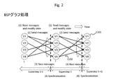
- FIG. 2 is a diagram for explaining BSP graph processing.
- the vertex 1101 includes a vertex ID for identifying the vertex 1101.
- V1 to V4 are vertex IDs.
- Data output during the processing of each vertex 1101 is a message 1102.
- the message 1102 is attached with a destination indicating one vertex 1101 that is related to the output source vertex 1101.
- the destination vertex receives the message 1102 and performs processing.
- the process from the start of the processing of the first vertex 1101 to the completion of the processing of the last vertex 1101 is called a super step. Synchronization is performed for each super step.
- the vertex inputs a message addressed to itself (read messages), and the vertex executes a process to update the state of the vertex (modify state).
- the vertex outputs a message for the next destination vertex (send message).
- the destination vertex receives the output message (Recv messages). (4)
- the super step S is completed (synchronization), and the process proceeds to the next super step S1.
- the message size is smaller than the block size of the non-volatile memory.
- data is frequently fragmented and GC is frequently performed.
- valid data in the erase block must be moved to another block. Therefore, extra fragmentation occurs when fragmentation occurs. That is, the number of block erasures increases and the lifetime of the nonvolatile storage medium is shortened.
- the computer system according to the present embodiment can reduce the number of block erasures by reducing GC by writing a plurality of messages to a specific physical storage area and erasing the plurality of messages at a time. It is possible to prevent the life of the product from being shortened. Furthermore, it is possible to prevent a decrease in the access performance of the nonvolatile memory due to the GC.
- FIG. 3 shows a configuration of a computer system according to the present embodiment.
- the computer system is a system in which a nonvolatile memory device 101 and a host computer (hereinafter referred to as a host) 102 are connected via a communication network.
- the non-volatile memory device 101 and the host 102 may communicate with the same communication protocol (for example, PCI Express (registered trademark)) as the communication protocol in the non-volatile memory device 101 and the communication protocol in the host 102 or different communication. Communication may be performed using a protocol (for example, Fiber Channel).
- the computer system may be a converged system in which the nonvolatile memory device 101 and the host 102 are housed in one housing.
- the nonvolatile memory device 101 is, for example, a storage media drive (for example, SSD; Solid State Drive) having one or more memory chips 111. Further, the nonvolatile memory device 101 may be a large-scale memory system having a plurality of nonvolatile memory devices 101. In the present embodiment, the nonvolatile memory device 101 is described as a media drive having one or more memory chips 111, a controller 112, a chunk information register 114, and a host I / F 118. These elements may be connected to each other by, for example, a bus (for example, a PCI Express bus).
- a bus for example, a PCI Express bus
- the memory chip 111 is a NAND flash memory in this embodiment. Therefore, the memory chip 111 is composed of a plurality of blocks, and each block is composed of a plurality of physical pages. Data is read / written for each physical page and data is erased for each block. That is, a physical page is a data writing unit, and a block is a data erasing unit.
- the memory chip 111 is replaced with other types of non-volatile memories (for example, MRAM (Magnetoretic Random Access Memory), ReRAM (Resistant Random Access Memory), or FeRAM (Ferroelectric Random Memory) instead of NAND flash memory. Good.
- the controller 112 is a module including a CPU (Central Processing Unit) (for example, a CPU itself or a module including a CPU and dedicated hardware such as DMA).
- the controller 112 performs processing in response to a request from the host 102.
- the controller 112 controls data transfer within the nonvolatile memory device 101.
- a CPU Central Processing Unit
- DMA dedicated hardware
- the chunk information register 114 is a storage area provided in a memory (not shown) in the nonvolatile memory device 101.
- the memory may be a volatile memory or a non-volatile memory.
- the memory is, for example, a DRAM (Dynamic Random Access Memory). Chunk information described later is stored in the chunk information register.
- the host I / F 113 is an interface device connected to the host 102.
- the host 102 includes a CPU 121, a main memory 122, and a nonvolatile memory I / F 123.
- the CPU 121 controls the operation of the host 102.
- the main memory 122 is a memory that the host 102 has.
- the main memory 122 is, for example, a DRAM, but other types of memory may be employed instead of the DRAM 122.
- the nonvolatile memory I / F 123 is an interface device connected to the host I / F 113 of the nonvolatile memory device 101.
- the host 102 may have a non-volatile memory (hereinafter, program memory) that stores a program executed by the CPU 121.
- program memory non-volatile memory
- a program may be loaded from the program memory into the main memory 122 and the program loaded into the main memory 122 may be executed by the CPU 121. There may be no program memory, and a program executed by the CPU 121 may be loaded from the memory chip 111 of the nonvolatile memory device 101 to the main memory 122.
- the host 102 may be connected to an input device (not shown) for inputting data such as a user code (to be described later) by the user and an output device (not shown) for displaying the processing result to the user.
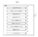
- FIG. 4 shows an example of information stored in the main memory 122 of the host 102.
- the main memory 122 includes a user code program 221, a graph framework (graph FW) program 222, a current address table 223, a previous address table 224, a chunk set allocation table 225, a free chunk set list 226, and a chunk set.
- An empty list table 227 and management middleware 228 are stored. As described above, these pieces of information may be stored in the program memory, or may be temporarily read from other places into the main memory 122 and used.
- a working area 229 for reading data necessary for graph processing is secured in the main memory 122.
- the user code program 221 is a program that specifies the contents of the graph processing by the user code input by the user.
- the graph FW program 222 is a program that executes graph processing.
- the management middleware 228 is a program that controls these programs 221 and 222, and is, for example, an OS.
- the user code program 221 specifies the size of the logical address according to the input from the user to the graph framework program 222.
- the graph framework program 222 requests the management middleware 228 for the specified logical address size.
- the management middleware 228 secures a storage area of the usable memory chip 111 based on the size of the logical address included in the request, and displays the range of usable logical addresses (start logical address and end logical address) in the graph frame.
- the work program 222 is notified. The description of each information 223 to 227 will be described later.
- FIG. 5 shows the configuration of a program related to graph processing.
- the user code program 221 and the graph framework program 222 are executed on the management middleware 228.
- the user code program 221 includes each vertex calculation processing unit 301.
- the graph framework program 222 includes a calculation processing order control unit 311, a calculation processing unit 312, a data communication processing unit 313, a writing processing unit 314, and a reading processing unit 315.
- the write processing unit 314 includes a grouping processing unit 321 and an address management unit 322. Each of these units is, for example, a program module.
- Each vertex calculation processing unit 301 is designated by a user code and indicates processing of each vertex.
- the calculation processing order control unit 311 controls the order of calculation processing in the calculation processing unit 312.
- the calculation processing unit 312 executes the processing of each vertex calculation processing unit 301.
- the data communication processing unit 313 controls message communication between 312 and 314.
- the writing processing unit 314 controls writing of data to the nonvolatile memory.
- the grouping processing unit 321 groups data.
- the address management unit 322 manages logical addresses.
- the read processing unit 315 controls reading of data from the nonvolatile memory.
- FIG. 6 is a diagram showing a connection state inside the nonvolatile memory device 101.
- the controller 112 has a plurality of DMA (Direct Memory Access) 115.
- the DMA 115 is a hardware circuit that controls data transfer.
- Each DMA 115 is connected to a plurality of memory chips 111 via a bus 116.
- a plurality of DMAs 115 in the controller 112 may be described with DMAID (#) attached.
- the controller 112 has 16 DMAs, DMA # 0 to DMA # 15.
- CEID (#) may be attached to a plurality of memory chips 111 connected to each DMA.
- 16 memory chips 111, CE # 0 to CE # 15 are connected to each DMA.
- the controller 112 may not have the DMA 115. In this case, the controller 112 controls data transfer in the nonvolatile memory device 101.
- FIG. 7 is a diagram showing the relationship between logical pages and chunks.
- the controller 112 sets a chunk 920 and a chunk group 960 including a plurality of chunks 920.
- the chunk group 960 is a matrix of a plurality of chunks 920.
- the controller 112 assigns each memory chip 111 to one chunk 920.
- the number of chunks (number of horizontal chunks) arranged in the horizontal (row) direction of the chunk group 960 corresponds to the number of DMAs 115 (16).
- the number of chunks arranged in the vertical (column) direction of the chunk group 960 corresponds to the number of memory chips 111 connected to one DMA 115 via the bus (the number of CEs, 16).
- the controller 112 defines each row in the chunk group 960 as a chunk set (see FIG. 9).
- the number of vertical chunks is the same as the number of chunk sets, and the number of horizontal chunks is the same as the number of chunks in each chunk set.
- the controller 112 sets a plurality of logical pages 922 in each chunk 920.
- the controller 112 associates a logical address with each logical page.
- the controller 112 manages the logical page 922 with the same size as the physical page in each memory chip 111, but may manage it with a different size.
- the controller 112 allocates a plurality of logical blocks 925 to each chunk 920.
- the logical block 925 is managed with the same size as the physical block 930 in each memory chip 111, but may be managed with a different size.
- the controller 112 allocates consecutive chunk numbers to the chunks 920 in the chunk group 960. For example, the controller 112 chunks chunks 960 in the chunk group 960 so that each chunk 920 in the first row is chunks # 00 to # 15 and each chunk 920 in the second row is chunks # 16 to # 31. Allocate 00 to # 255.
- the controller 112 assigns a logical block 925 to each chunk 920 in the chunk group 960. For example, the controller 112 assigns one logical block (B # 00) to the first column chunk (CHUNK # 00) in the first row, and then assigns it to the second column chunk (CHUNK # 01) in the first row. After allocating one logical block (B # 01) and allocating one logical block (B # 015) to the last column chunk (CHUNK # 015) of the first row, the first column chunk (second row) One logical block is allocated to CHUNK # 016).
- the controller 112 assigns logical blocks one by one to the last (16) column chunk (CHUNK # 225) of the last (16) row, and then again starts from the first chunk (CHUNK # 00) of the chunk group.
- a plurality of logical blocks are allocated to all the chunks 920 in the chunk group 960, such that the second logical block is allocated. That is, the controller 112 first assigns the first logical block in order of the chunk number to all chunks 920 in the chunk group 960, and then assigns the second logical block in order of the chunk number. Allocate logical blocks until each chunk is full.
- Controller 112 allocates logical page 922 to logical block 925.
- the number of chunk interleaved LPs is the number of logical pages 922 continuously allocated to each chunk 920.
- the number of chunk interleaved LPs is two.
- the controller 112 assigns two logical pages # 0 and # 1 to the first logical block (B # 00) in the first chunk in the chunk group in the order of logical page numbers.
- Logical pages # 2 and # 3 are allocated to the first logical block (B # 01) in the two-column chunk, and the first logical block (B # 15) in the fifteenth column of the first row is allocated.
- logical pages # 31 and 32 following the first logical block (B # 00) in the chunk of the first column in the first row are allocated.
- the controller 112 assigns all logical pages to the first logical block (B # 00 to 15) of each chunk in the first row, and then the first logical in the second row and each column. Assign logical pages to blocks in the same way.
- the controller 112 assigns a logical page to the first logical block of each column in the last row in the same manner, and then similarly assigns a logical page to the second logical block of each column in the first row. Assign.
- the controller 112 allocates logical pages 922 to each chunk 920 in the chunk group 960 up to a predetermined number of LPs in the chunk group.
- the number of LPs in the chunk group is, for example, a value (integer value) obtained by dividing the logical page number that can be arranged in the chunk group by the number of chunks in the chunk group in order to uniformly arrange the number of logical pages in each chunk. It may be a value obtained by multiplying the number of vertical chunks by the number of horizontal chunks.
- controller 112 identifies the corresponding chunk from the logical address.
- the controller 112 includes the page size of the logical page, the number of LPs in the chunk group 960, the number of LPs in the logical block 925, the number of horizontal chunks in the chunk group 960 (number of chunk sets, number of DMAs), chunk group The number of vertical chunks in 960 (number of chunks in chunk set, number of chunks connected to one DMA) and number of chunk interleaved LPs are stored.
- the controller 112 corresponds to each logical address, the logical page number (#), the chunk group number (#), the intra-chunk group logical page number (#), the intra-chunk group logical page number (#), The horizontal chunk number (#) and the vertical chunk number (#) are calculated.
- the calculation method of these values is as follows.
- Logical page number (#) logical address / page size
- chunk group number (#) logical page number (#) / number of LPs in chunk group
- LP number in chunk group (#) LP Number% Number of LPs in chunk group
- Vertical chunk number (#) (Number of LPs in chunk group / (Number of LPs in logical block * Number of horizontal chunks))% Number of vertical chunks in chunk group)
- Horizontal chunk number (#) (LP number in chunk / number of chunk interleaved LPs)% Number of horizontal chunks in chunk group
- the controller 112 is based on the vertical chunk number (#) and the horizontal chunk number (#). You may calculate the chunk number (#) which can specify each chunk uniquely within a chunk group.
- the controller 112 can specify a chunk from a logical address using the above formula.
- controller 112 transmits chunk information to the host 102.
- the host 102 can determine the range of logical addresses corresponding to each chunk set using the chunk information transmitted from the controller 112.
- FIG. 8 is a diagram for explaining logical-physical conversion by the controller 112.
- the memory chip 111 includes a plurality of physical blocks. Each physical block includes a plurality of physical pages.
- a logical page may be described as an L page and a physical page as a P page.
- the host 102 determines the logical address 911 based on the chunk information, designates the logical address 911, and transmits a command to the nonvolatile memory 101.
- the controller 112 receives a write command designating a logical address from the host 102, the controller 112 identifies a logical page and chunk corresponding to the logical address, and selects a free physical block from the memory chip 111 corresponding to the chunk. . Then, the controller 112 allocates a free physical page 933 from the top in the selected physical block 930 to the logical page 922. Thereby, the storage location of the write data is determined.
- the controller 112 identifies L page # 0 and chunk # 0 corresponding to LBA0x00, and an empty block in the memory chip # 0 corresponding to chunk # 0 # 00 is selected, P page # 00 in block # 00 is selected, P page # 00 is assigned to L page # 00, and write data according to the write command is written to P page # 0.
- the controller 112 assigns the memory chip 111 and the chunk 920 on a one-to-one basis.
- the present invention is not limited to this mode.
- the controller 112 erases data for each physical block 930 that is an erase unit. In this case, the controller 112 determines whether or not the number of free physical blocks has fallen below a preset threshold value, and when it falls, the valid page in the physical block having the highest invalid page rate is copied to another physical block. The GC is executed. The controller 112 erases data in the physical block that has become all invalid pages by GC, thereby making the physical page in the physical block an empty page in which data can be stored.
- the write data written in different chunks 920 is always stored in different physical blocks 930.
- the chunk information is notified from the controller 112 to the host 102.
- the host 102 can select the chunk set of the write data storage destination.
- the host 102 can store unnecessary data in a single chunk set based on preset conditions. Specifically, a plurality of data that becomes unnecessary and invalidated at the first timing are collectively stored in a plurality of physical blocks 930 corresponding to the first chunk set, erased collectively, and made into empty blocks. be able to. Thereby, GC can be reduced.
- the host 102 can store unnecessary data based on different conditions in another chunk set. Data that becomes unnecessary and invalidated at the first timing can be stored in the first chunk set, and data that becomes unnecessary and invalidated at the second timing can be stored in the second chunk set. Therefore, it is possible to prevent data that becomes unnecessary and invalidated at the first timing and data that becomes unnecessary and invalidated at the second timing from being stored in the same physical block.
- the controller 112 transfers the write data to each memory chip 111 allocated in the chunk set. Can be distributed and stored. As a result, it is possible to prevent the bias of deterioration between the memory chips 111.
- FIG. 9 is a diagram for explaining the relationship between chunks, chunk sets, and chunk groups.
- the chunk group includes a plurality of chunk sets.
- the invalidation unit is a chunk set to which a plurality of physical blocks that are data erasure units are assigned.
- data stored in the invalidation unit is, for example, a message group in BSP graph processing.
- the size of each message is smaller than the block size.
- BSP graph processing a large number of vertices are processed at each superstep. For this reason, the number of messages output from the apex also increases.
- the non-volatile memory device 101 of this embodiment can prevent data fragmentation and reduce the number of GCs by setting an invalidation unit to which a plurality of erase units are assigned. Note that a chunk set that is an invalidation unit stores a set of messages destined for one vertex set in one super step.
- a chunk set vertical chunk
- the number of DMAs 115 buses 116
- the chunk set can be changed by the user according to the usage status.
- the user may set a part of the memory chip 111 connected to each DMA 115 (bus 116) as a chunk set, or collect a plurality of chunks 920 connected to one or a plurality of DMAs 115 (bus 116).
- a chunk set may be set.
- FIG. 10 is a diagram for explaining the grouping process of the vertex 1101.
- the vertex grouping process is executed by the grouping processing unit 321.
- the grouping processing unit 321 distributes all vertices 1101 executed in each BSP graph process to the vertex group 1103.
- the vertex group 1103 is defined by the size of the working area 229 in the main memory 122 necessary for reading the vertex 1101. In other words, the total size of messages input to one vertex group in one superstep is less than or equal to the size of the working area 229.
- the host 102 determines the number of vertices belonging to the vertex group according to the vertex data read out to the working area 229 and the message size.
- a remainder value obtained by dividing the vertex ID of each vertex 1101 by the number of vertex groups (g) is set as the vertex group ID.
- the distribution method is not limited to the above method. For example, a method of assigning to vertex groups in the order of vertex IDs may be used.
- each vertex calculation processing unit 301 defines each vertex, and the calculation processing unit 312 executes processing for each vertex according to an instruction from the calculation processing order control unit 311.
- Each vertex may be processed in parallel by a plurality of CPUs 121, or may be processed in parallel by a plurality of cores in CPU 121. Further, each vertex need not be processed strictly in parallel by a plurality of CPUs 121 (or cores) as long as it is processed in batches for each super step.
- FIG. 11 is a diagram for explaining the order of processing of the vertex groups in the super step.
- the calculation processing order control unit 311 performs control so that each vertex 1101 is processed for each vertex group 1103 in the super step.
- the read size of the vertices 1101 and the message 1102 can be made smaller than the size of the working area 229 of the main memory 122. That is, the number of vertices 1101 in the vertex group 1103 can be determined so as to be equal to or smaller than the size of the working area 229.
- the calculation processing order control unit 311 stores the determined number of vertices 1101 in the working area 229 of the main memory 122.
- calculation processing order control unit 311 may determine the processing order of the vertex groups before the processing of each super step or before the execution of the graph processing. Further, the number of vertices processed in the graph processing, the number of vertices belonging to the vertex group, and the number of vertex groups may be set by the user in the user code program of the host 102.
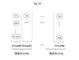
- FIG. 12 is a diagram for explaining a vertex set.
- the host 102 satisfies a preset condition, the host 102 defines a vertex set including a plurality of vertex groups 1103. For example, since one vertex group uses two chunk sets, the calculation processing order control unit 311 lacks chunk sets when the number of chunk sets is less than twice the number of vertex groups. Define. In this embodiment, a case where a vertex set is defined will be described.
- the host 102 allocates one chunk set as a storage destination of the message 1102 destined for each vertex of one vertex set.
- One vertex set may be one vertex group.
- the calculation processing order control unit 311 assigns a plurality of vertex groups to one vertex set. include.
- a read chunk set for storing a message input to one vertex set during one super step, and a message for storing a message output with each vertex of the vertex set as a destination.
- Two chunk sets can be prepared, including a built-in chunk set.
- the number of vertices included in the vertex group is set according to the size of the working area 229. For this reason, when the number of vertex groups exceeds twice the number of chunk sets, all vertex groups can be assigned to the chunk sets by defining the vertex set.
- FIG. 13 is an example of an address table.
- the host 102 has two address tables, a current address table 223 and a previous address table 224.
- the current address table 223 is a logical page that stores messages 1102 that are processed and output by each vertex group 401 in the super step (current super step) being executed and the vertex 1101 in each vertex group 1103 in the BSP graph processing.
- 10 is a table for associating an address list 402 that is a list of logical addresses of 922; For example, in the address list 402, a logical address indicating the logical page 922 included in the chunk set assigned to each vertex group 1103 is set.
- the previous address table 224 is processed at the vertex group 1103 that is the destination of the message that is output in the super step immediately before the current super step (previous super step), and each vertex 1101 in each vertex group 1103. 3 is a table that associates the logical address of the message 1102 to be processed.
- These address tables 222 and 223 have the same configuration. Hereinafter, a common configuration of these address tables will be described.
- the address table has an entry for each vertex group 1103. Each entry has a Group ID 401 that identifies the vertex group 1103 and an address list 402 that is a list of logical addresses of the logical page 922 in which a message 1102 destined for each vertex 1101 in the vertex group 1103 is stored.
- FIG. 14 is an example of the chunk set allocation table 225.
- the chunk set allocation table 225 is a table that associates a vertex set composed of a plurality of vertex groups with a chunk set composed of a plurality of chunks.
- the chunk set allocation table 225 has an entry for each vertex set. Each entry has a vertex set number (#) 501 that is an identifier of the vertex set and a chunk set number (#) 502 that is an identifier of the chunk set.
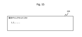
- FIG. 15 is an example of the empty chunk set list 226.
- the free chunk set list 226 is a list of chunk sets that are not assigned to the vertex set.
- FIG. 16 is an example of the chunk set empty list table 227.
- the chunk set empty list table 227 is a table that associates a chunk set with a logical address of a logical page 922 in the chunk set.
- the chunk set empty list table 227 has an entry for each chunk set. Each entry has a chunk set number (#) 701 that is an identifier of the chunk set, and a free address list 702 that is a list of logical addresses indicating logical pages that are not allocated to any chunk set.
- # chunk set number
- FIG. 17 is a diagram for explaining grouping processing and writing processing of the message 1102.
- the grouping process and the writing process for the message 1102 are executed by the writing processing unit 314.
- a message 1102 input / output during the processing of the vertex 1101 includes a destination vertex ID for identifying a destination vertex (destination vertex).
- the writing processing unit 314 calculates a group ID and a local vertex ID in the group from the destination vertex ID included in the message. For example, the write processing unit 314 calculates the group ID and the local vertex ID by dividing the destination vertex ID by the number of vertex groups.
- the method for calculating the group ID and the local vertex ID from the destination vertex ID is not limited to the method described above.
- the main memory 122 has a buffer 1502 for storing the message 1102 of the vertex group 1103.
- the buffer 1502 is provided in the working area 229 of the main memory 122.
- a buffer 1502 is provided for each vertex group indicated by the group ID.
- Gr. 2 is the group ID of the vertex group.
- the write processing unit 314 stores the message 1102 in the buffer 1502 specified by the calculated group ID.
- the write processing unit 314 executes a write process.
- the writing processing unit 314 transmits the message 1102 in the buffer 1502 to the nonvolatile memory device 101.
- the write processing unit 314 refers to the current address table 223, and issues a write instruction specifying a logical address included in the address list 402 corresponding to the calculated group ID 401 to the nonvolatile memory device 101.
- the controller 112 of the nonvolatile memory device 101 refers to the chunk information and stores the message 1102 in the physical page corresponding to the logical page indicated by the designated logical address.
- the write processing unit 314 empties the contents of the buffer 1502 that has written.
- the previous address table 224 is a table for reading a message for the destination vertex.
- the message 1102 can be collected for each destination vertex group by the message grouping process.
- each address table 223 is associated with a vertex group 1103 and a logical address indicating a logical page in the corresponding chunk set. Therefore, the message 1102 destined for each vertex in the vertex group 1103 can be stored in the chunk set assigned to the vertex set including the vertex group 1103. As a result, the vertex set messages can be collectively stored in the chunk set which is the invalidation unit.
- FIG. 18 is a diagram for explaining the message 1102 reading process.
- the message reading process is executed by the reading processing unit 315.
- the read processing unit 315 reads a message necessary for executing the vertex to the working area 229 of the main memory 122. Specifically, for example, the read processing unit 315 refers to the previous address table 224 and acquires a logical address corresponding to the vertex group 1103.
- the read processing unit 315 transmits a read command specifying the acquired logical address to the nonvolatile memory device 101. For example, when reading the message 1102 necessary for executing each vertex 1101 of the vertex group # 2 to the main memory 122, the read processing unit 315 refers to the previous address table 224 and sends a read command designating the logical addresses A to E. Transmit to the non-volatile memory device 101.
- the calculation processing order control unit 311 refers to the all address table 224 and sets logical addresses corresponding to all the vertex groups 1103 included in the vertex set.
- the designated trim command is transmitted to the nonvolatile memory device 101.
- the trim command is a command for notifying a logical address in which unnecessary data is stored.
- the host 102 of this embodiment notifies the non-volatile memory device 101 of a logical address of a message that is no longer necessary for each vertex set in one super step by a trim command.
- the controller 112 that has received the read command reads out the message 1102 stored in the physical page corresponding to the designated logical address based on the chunk information and transmits it to the host 102. Then, the controller 112 that has received the trim command cancels the allocation of the designated logical address to the target physical page, and invalidates the target physical page.
- messages 1102 necessary for the processing of the vertices of the vertex group 1103 can be collectively read.
- the physical page in which the read message 1102 is stored can be invalidated for each chunk set corresponding to the vertex set.
- messages used by one vertex set are collectively stored in one chunk set. For this reason, messages in one chunk set are invalidated together. Therefore, the number of GC can be reduced.
- the writing processing unit 314 discards the contents of the previous address table 224 and copies the contents of the current address table 223 to the previous address table 224.
- FIG. 19 illustrates a flowchart of the write range control process according to the present embodiment.
- This process is a process executed by the host 102 when the BSP graph process starts.
- initial data including the vertex 1101 necessary for the BSP graph processing is stored in a storage device (not shown) (for example, SSD, HDD; Hard disk drive, etc.) different from the nonvolatile memory device 101.
- the calculation processing order control unit 311 executes initialization processing (S901). Details of the initialization process will be described later.
- initialization processing a logical address range used for the BSP graph process is set, and the chunk group 960 that can be used and the number of chunk sets in the chunk group 960 are calculated based on this logical address range. Then, the logical address range of the chunk set is assigned to the vertex set, and the chunk set assignment table 225 is generated.
- the calculation processing order control unit 311 stores the initial data, which is the initial value of each vertex used for the BSP graph processing, in one or more chunk sets, and updates the free chunk set list 226 (S902). For example, the calculation processing order control unit 311 calculates the logical address of the logical page corresponding to each chunk set, and transmits a read command designating the logical address to the nonvolatile memory device 101. In this case, for example, the calculation processing order control unit 311 may collect initial data for each vertex group 1103 and store them in a chunk set.
- the controller 112 of the nonvolatile memory 101 receives the initial data and stores the initial data in the physical page 933 corresponding to the chunk set.
- the calculation processing order control unit 311 repeats the vertex group processing (S903 to S906).
- the vertex group process will be described below.
- a vertex group that is a target of vertex group processing is referred to as a target vertex group.
- the calculation processing order control unit 311 refers to the previous address table 224 and executes a reading process of reading a message having each vertex of the target vertex group as a destination vertex to the main memory 122 (S903).
- the reading process is as described in FIG. Specifically, for example, the calculation processing order control unit 311 refers to the previous address table 224 and acquires a logical address included in the address list 402 corresponding to the vertex group ID 401 of the target vertex group. Then, the calculation processing order control unit 311 transmits a read command specifying the acquired logical address to the nonvolatile memory device 101.
- the calculation processing order control unit 311 adds the acquired logical address to the free address list 702 of the chunk set free list table 227.
- controller 112 of the non-volatile memory device 101 transmits the message 1102 stored in the physical page corresponding to the logical address specified by the read command based on the chunk information to the host 102 by the reading process.
- the calculation processing order control unit 311 receives the message 1102 and stores the received message 1102 in the main memory 122.
- the calculation processing order control unit 311 hands over the processing to the calculation processing unit 312.
- the calculation processing unit 312 executes processing for the vertex 1101 (S904).
- the calculation processing unit 312 delivers the message 1102 generated by executing the processing of each vertex 1101 to the data communication processing unit 313.
- the data communication processing unit 313 delivers the message 1102 to the writing processing unit 314 (to S911).
- the calculation processing order control unit 311 determines whether or not the target vertex group is the last group to execute this processing in the vertex set (S905). When it is not the last vertex group (S905; No), the calculation processing order control unit 311 returns the processing to S903.
- the calculation processing order control unit 311 refers to the previous address table 224, and for each vertex group from the address list 402 corresponding to the vertex group ID 401 of each target vertex group in S903. The logical address in which the message 1102 read out is stored is acquired. Then, the calculation processing order control unit 311 transmits a trim command specifying the acquired logical address to the nonvolatile memory device 101. The calculation processing order control unit 311 adds the acquired chunk set number (#) to the free chunk set list 226, and advances the processing to S907.
- the controller 112 invalidates the physical page corresponding to the logical address specified by the trim command.
- the write processing unit 314 receives a message from the calculation processing order control unit 311 via the data communication processing unit 313 (S911).
- the write processing unit 314 executes a message grouping process for grouping the received message 1102 for each destination vertex (S912).
- the grouping process is as described with reference to FIG.
- a message with the vertex group vertex as the destination is stored in the buffer 1502 for each vertex group.
- the write processing unit 314 determines whether or not there is a buffer area 1502 filled with the message 1102 in the working area 229 (buffer full) (S913). When there is a buffer area 1502 that is filled with the message 1102 (S913; Yes), the write processing unit 314 performs a write process (S914) and advances the process to S915.
- the outline of the writing process is as described in FIG. Details of the writing process will be described later.
- the write processing unit 314 advances the process to S915.
- the writing processing unit 314 determines whether or not the super step is completed (S915). If the super step has not ended (S915; No), the write processing unit 314 returns the process to S911. On the other hand, when the super step is finished (S915; Yes), the writing processing unit 314 notifies the calculation processing order control unit 311 that the super step is finished, and waits.
- calculation processing order control unit 311 When the calculation processing order control unit 311 receives the notification from the writing processing unit 314 and completes the vertex group processing of the plurality of vertex groups 1103 in the vertex set, the calculation processing sequence control unit 311 advances the processing to S907.
- the calculation processing order control unit 311 determines whether or not the BSP graph processing is finished (S907). When it is determined that the BSP graph processing has not ended (S907; No), the calculation processing order control unit 311 updates the chunk set allocation table 225 so as to deallocate the chunk set and the vertex group (S908), and the previous address The information in the table 224 is discarded, the data in the current address table 223 is copied to the previous address table 224, and the process returns to S903. Thereby, the next super step is started.
- a physical block in which a message group destined for each vertex set is stored by storing unnecessary messages after being used for vertex processing in a chunk set for each vertex set. Can be limited. Thereby, even when a very large number of vertex processes are executed, such as a BSP graph process, frequent occurrence of GC in the nonvolatile memory device 101 can be prevented. Accordingly, it is possible to prevent a decrease in the lifetime of the nonvolatile memory and a decrease in the access performance of the nonvolatile memory.
- the message 1102 becomes unnecessary when the processing of the vertex 1101 of the destination (input destination) of the message 1102 is completed.
- the vertex set By setting the vertex set, messages 1102 that become unnecessary at a certain timing can be collectively stored in the same chunk set.
- an invalidation instruction (trim command) is transmitted to the nonvolatile memory device 101, whereby the physical block assigned to the chunk set corresponding to the vertex set is transmitted. Can be erased together. Therefore, fragmentation of data in the physical block can be prevented, the number of GCs can be reduced, and a decrease in the lifetime of the nonvolatile memory can be prevented.
- the chunk set by configuring the chunk set with a plurality of chunks based on the hardware configuration, for example, with a plurality of chunks corresponding to the memory chips 111 respectively connected to all the buses in the nonvolatile memory device 101 one by one.
- the access performance of the host 102 to the nonvolatile memory device 101 can be improved.
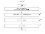
- FIG. 20 is a flowchart of the initialization process.
- the initialization process is the process of S901 in the writing range control process.
- the address range of the non-volatile memory device 101 that the user wants to use in the BSP graph processing is specified via the user code program 221, and the management middleware uses the logical address range (logical address size or start logical address-end logical address). ) Is determined, the calculation processing order control unit 311 of the framework program 222 is activated (S801).
- the calculation processing order control unit 311 determines a chunk group 960 as a range of chunks 920 that can be used for BSP graph processing based on the determined logical address range and the chunk information received from the nonvolatile memory device 101 (S802). .
- the calculation processing order control unit 311 may use the chunk group number of the chunk group 960, the chunk number (vertical chunk number and horizontal chunk number) of each chunk 920 in the chunk group 960, the number of chunks in the chunk group 960, and the like. May be calculated.
- the calculation processing order control unit 311 may generate and store logical-physical conversion information that associates the logical page in the chunk with the physical page in the memory chip based on the chunk information.
- the calculation processing order control unit 311 calculates the number of chunk sets based on the calculation result and chunk information in S802 (S803). For example, the calculation processing order control unit 311 calculates a value obtained by dividing the number of chunks in the chunk group 960 by the number of horizontal chunks (the number of DMAs in the nonvolatile memory device 101) as the number of chunk sets.
- the calculation processing order control unit 311 determines the number of vertex sets according to the number of chunk sets (S804). The method for calculating the number of vertex sets is as described with reference to FIG. The calculation processing order control unit 311 creates the determined number of vertex sets.
- the host 102 can calculate the number of chunk sets and the like based on the chunk information transmitted from the nonvolatile memory device 101, and generate a vertex set corresponding to each chunk set.
- FIG. 21 is a flowchart of the writing process.
- the writing process is the process of S914 in the writing range control process.
- the vertex group to be written is referred to as a writing vertex group.
- the write processing unit 314 calculates the vertex set ID of the vertex set (write vertex set) to which the write vertex group belongs from the vertex group ID of the write vertex group (S1002).
- the write processing unit 314 refers to the chunk set allocation table 225, (a) a chunk set (write chunk set) corresponding to the write vertex set is set, and (b) an empty address in the write chunk set It is determined whether or not exists. In the case of (a) and (b), the writing processing unit 314 advances the processing to S1007. On the other hand, if the write processing unit 314 does not satisfy at least one of the requirements (a) and (b), the process proceeds to S1004.
- the write processing unit 314 refers to the free chunk set list 226 and determines whether there is a free chunk set (S1004). If there is an empty chunk set (S1004; Yes), any empty chunk set is set in the writing vertex set, and the chunk set allocation table is updated (S1006). Then, the writing processing unit 314 advances the processing to S1007.
- the writing processing unit 314 refers to the chunk set allocation table 225 and the chunk set empty table 227, and sets a vertex set different from the vertex set of the writing vertex set.
- a chunk set that is a corresponding chunk set and has a free address is acquired (S1005).
- the writing processing unit 314 may acquire a chunk set corresponding to a vertex set having an ID close to the ID of the writing vertex set.
- the writing processing unit 314 sets the acquired chunk set as the writing vertex set (S1006), and advances the processing to S1007.
- the write processing unit 314 refers to the chunk set free list table 227, acquires a free address (logical address) corresponding to the set chunk set, and updates the free address list (S1007). Specifically, the write processing unit 314 deletes the acquired logical address from the free address list 226.
- the write processing unit 314 transmits a logical address corresponding to a message addressed to each vertex of the write vertex group to the nonvolatile memory device 101 (S1008).
- the controller 112 of the nonvolatile memory device 101 receives the logical address, and stores the message in the physical page corresponding to the received logical address based on the chunk information.
- a message can be stored in the chunk set assigned to the vertex set to which the writing vertex group belongs (writing vertex set).
- the vertex A write vertex set can be assigned to another free chunk set to which no set is assigned, and a message can be stored in that chunk set.
- the host 102 assigns one chunk set to one vertex set, and in one super step, a plurality of vertex groups in one vertex set are destined, and an input message is sent to one chunk set. Write to.
- the host 102 assigns one chunk set to one vertex set, and in one super step, a plurality of vertex groups in one vertex set are destined, and an input message is sent to one chunk set. Write to.
- it is not limited to this mode.
- the host 102 may assign one chunk to one vertex group and write a message 1102 input with one vertex group 1103 as the destination in one superstep to one chunk 920.
- the host 102 specifies a chunk number corresponding to the vertex group number using the chunk information, and writes a message in the logical address range corresponding to the chunk number.
- the write range control process can be executed in smaller units.
- the storage device corresponds to the nonvolatile memory device 101
- the processor corresponds to the CPU 121
- the storage device corresponds to the main memory 122.
- the first limited logical area and the second limited logical area correspond to different chunk sets or different chunks.
- the limited information corresponds to chunk information
- the specific command corresponds to a trim command.
- the processing data corresponds to the message.
- the limited logical area information corresponds to the chunk set allocation table 225, the empty chunk set list 226, the chunk set empty list table 227, and the like.
Abstract
According to the present invention, a storage device stores limit information about the size of a first limited logical region, which is a part of a logical storage region of a nonvolatile memory, associates a first physical storage region, which is a part of a physical storage region of the nonvolatile memory, with the first limited logical region on the basis of the limit information, and transmits the limit information to a host computer. The host computer performs a first process, thereby generating first processed data. The host computer calculates a range of first logical addresses indicating the first limited logical region, on the basis of the limit information, and transmits, to the storage device, the first processed data and a first write command specifying a particular first logical address within the range of first logical addresses. After the completion of the first process, the host computer transmits a read command specifying the particular first logical address to the storage device, and further transmits, to the storage device, a specific command indicating that the range of first logical addresses is no longer necessary.
Description
本発明は、不揮発性半導体メモリを用いた計算機システムに関する。
The present invention relates to a computer system using a nonvolatile semiconductor memory.
近年、HDD(Hard Disk Drive)に代えて又は加えて、不揮発性メモリを記憶媒体とするストレージ装置が用いられる。このような不揮発性メモリは、例えばNAND型のフラッシュメモリである。不揮発性メモリを記憶媒体とするストレージ装置は、複数の小型ディスクドライブを有するストレージ装置に比べて、省電力及びアクセス時間等に優れていると考えられている。
In recent years, a storage device using a nonvolatile memory as a storage medium is used instead of or in addition to an HDD (Hard Disk Drive). Such a nonvolatile memory is, for example, a NAND flash memory. A storage device using a non-volatile memory as a storage medium is considered to be superior in power saving, access time, and the like as compared to a storage device having a plurality of small disk drives.
フラッシュメモリは、メモリチップ内に複数のブロックが含まれる。ブロックはデータを一括消去する単位の記憶領域であり、ページはデータを読み書きする単位の記憶領域である。1つのブロック内に複数のページが設けられる。またフラッシュメモリは、特性上、記憶しているデータを直接書き換えることができない。記憶しているデータを書き換える場合、フラッシュメモリは、記憶している有効なデータを他のブロックに退避させた後、記憶しているデータをブロック単位で消去する。そして、フラッシュメモリは、消去したブロックにデータを書き込む。このように、フラッシュメモリにおけるデータの書換えは、ブロックごとのデータの消去を伴う。データの消去により、メモリチップは消耗する。このため、ブロック毎に消去可能な回数が規定されている。
Flash memory includes a plurality of blocks in a memory chip. A block is a storage area in a unit for erasing data collectively, and a page is a storage area in a unit for reading and writing data. A plurality of pages are provided in one block. Also, flash memory cannot directly rewrite stored data due to its characteristics. When the stored data is rewritten, the flash memory saves the stored valid data in another block and then erases the stored data in units of blocks. Then, the flash memory writes data to the erased block. As described above, rewriting of data in the flash memory is accompanied by erasure of data for each block. By erasing data, the memory chip is consumed. For this reason, the number of erasable times is defined for each block.
通常、フラッシュメモリに対するデータの書換え動作は、未使用領域へデータを追記する方式で行う。しかし、データの書換えが進むと、フラッシュメモリ内の未使用領域が少なくなるため、フラッシュメモリに書込まれている不要なデータを消去して記憶領域を再利用可能な状態にする必要が生ずる。旧データを含むブロック内の、有効なデータのみを未使用領域にコピーし、コピー元のブロックを消去して再利用可能な状態にするブロック再生処理が知られている。以下、これをガーベージコレクションと呼ぶ。場合によってはGCと省略して表記する。ガーベージコレクションは、無効データが多く含まれるブロックを対象に実行される。
* Normally, data rewrite operation to flash memory is performed by adding data to unused area. However, as the data rewrite progresses, the unused area in the flash memory decreases, so it becomes necessary to erase unnecessary data written in the flash memory so that the storage area can be reused. A block reproduction process is known in which only valid data in a block including old data is copied to an unused area, and the copy source block is erased to make it reusable. Hereinafter, this is called garbage collection. In some cases, it is abbreviated as GC. Garbage collection is performed on blocks that contain a lot of invalid data.
フラッシュメモリを用いたストレージ装置において、コントローラが、データのライト先の論理アドレスに従う論理ページに割り当てられている論理チャンクに割り当てられている物理領域を特定し、その特定した物理領域にデータを書き込む技術が知られている(特許文献1)。
In a storage device using flash memory, the controller specifies a physical area assigned to a logical chunk assigned to a logical page according to the logical address of the data write destination, and writes data to the specified physical area Is known (Patent Document 1).
一方、インターネット環境の発展により飛躍的に増加するオブジェクトを効率的に処理する技術として、例えば、グラフ処理が知られている(特許文献2)。グラフ処理において処理されるオブジェクトは年々増加している。
On the other hand, for example, graph processing is known as a technique for efficiently processing objects that dramatically increase due to the development of the Internet environment (Patent Document 2). The number of objects processed in graph processing is increasing year by year.
上述のように、ストレージ装置が処理するデータは、年々増加している。不揮発性メモリ含むストレージ装置において、膨大なデータ処理を行った場合、無秩序にデータを書き込めばデータの書換え動作が増加しGCが多発し、不揮発メモリの寿命が低下するおそれがある。
As described above, the data processed by the storage device is increasing year by year. In a storage device including a nonvolatile memory, when enormous data processing is performed, if data is written in a disorderly manner, the data rewriting operation increases, GC occurs frequently, and the lifetime of the nonvolatile memory may be reduced.
かかる課題を解決するために本発明に係る計算機システムは、ストレージ装置と、ストレージ装置に接続されるホスト計算機とを備える。ストレージ装置は、不揮発性メモリと、不揮発性メモリ及びホスト計算機に接続されるコントローラと、を含む。ホスト計算機は、記憶デバイスと、記憶デバイス及びストレージ装置に接続されるプロセッサと、を含む。コントローラは、不揮発性メモリの論理記憶領域の一部である第1限定論理領域のサイズに関する限定情報を記憶し、限定情報に基づいて、不揮発性メモリの物理記憶領域の一部である第1物理記憶領域を、第1限定論理領域に関連付ける。コントローラは、限定情報を、ホスト計算機に送信する。プロセッサは、第1処理を実行し、第1処理により第1処理データを生成する。プロセッサは、限定情報に基づき、第1限定論理領域を示す第1論理アドレス範囲を算出する。プロセッサは、第1論理アドレス範囲内の第1論理アドレスを指定した第1ライトコマンドと第1処理データとをストレージ装置へ送信する。コントローラは、第1ライトコマンドに応じて、第1物理記憶領域内の第1物理アドレスを、第1論理アドレスに割当て、第1物理アドレスにより示された領域に第1処理データを書き込む。プロセッサは、第1処理の後、第1論理アドレスを指定したリードコマンドをストレージ装置へ送信する。コントローラは、リードコマンドに応じて、第1物理アドレスにより示された領域から第1処理データを読出す。プロセッサは、第1論理アドレス範囲が不要であることを示す特定コマンドをストレージ装置へ送信する。コントローラは、特定コマンドの受信の後に、第1処理データを消去する。
In order to solve this problem, a computer system according to the present invention includes a storage device and a host computer connected to the storage device. The storage device includes a non-volatile memory and a controller connected to the non-volatile memory and the host computer. The host computer includes a storage device and a processor connected to the storage device and the storage apparatus. The controller stores limited information related to the size of the first limited logical area that is a part of the logical storage area of the nonvolatile memory, and based on the limited information, the first physical that is a part of the physical storage area of the nonvolatile memory. The storage area is associated with the first limited logical area. The controller transmits the limited information to the host computer. The processor executes the first process and generates first process data by the first process. The processor calculates a first logical address range indicating the first limited logical area based on the limited information. The processor transmits the first write command specifying the first logical address within the first logical address range and the first processing data to the storage device. In response to the first write command, the controller assigns the first physical address in the first physical storage area to the first logical address, and writes the first processing data in the area indicated by the first physical address. After the first process, the processor transmits a read command designating the first logical address to the storage device. In response to the read command, the controller reads the first processing data from the area indicated by the first physical address. The processor transmits a specific command indicating that the first logical address range is unnecessary to the storage device. The controller erases the first processing data after receiving the specific command.
データの書込範囲を制御することで、不揮発性半導体メモリの寿命および性能の低下を防止できる。
∙ By controlling the data writing range, it is possible to prevent the lifetime and performance of the nonvolatile semiconductor memory from deteriorating.
以下の説明では、「kkkリスト」、「kkkテーブル」、「kkk情報」の表現にて情報を説明することがあるが、情報は、どのようなデータ構造で表現されていてもよい。データ構造に依存しないことを示すため「kkkリスト」、「kkkテーブル」、「kkk情報」は、いずれの呼び方にも置換できる。さらに、各情報の内容を説明する際に、「ID」、「番号」、「識別子」という表現を用いるが、これらに代えて又は加えて他種の識別情報が使用されてよい。
In the following description, information may be described in terms of “kkk list”, “kkk table”, and “kkk information”, but the information may be expressed in any data structure. The “kkk list”, “kkk table”, and “kkk information” can be replaced by any name to indicate that they do not depend on the data structure. Furthermore, in describing the contents of each information, the expressions “ID”, “number”, and “identifier” are used, but other types of identification information may be used instead of or in addition to these.
また、以下の説明では、「プログラム」を主語として処理を説明する場合があるが、プログラムは、プロセッサによって実行されることで、定められた処理を、適宜に記憶資源(例えば、メモリ)及び/又は通信インターフェイスデバイス(例えば、通信ポート)を用いながら行うため、処理の主語がプロセッサとされてもよい。逆に、プロセッサが主語となっている処理は、1以上のプログラムを実行することにより行われると解釈することができる。
In the following description, the process may be described using “program” as a subject. However, the program is executed by the processor, so that the determined process can be appropriately performed with storage resources (for example, memory) and / or Alternatively, since the processing is performed using a communication interface device (for example, a communication port), the subject of processing may be a processor. On the contrary, the processing whose subject is the processor can be interpreted as being executed by executing one or more programs.
以下、ホスト計算機と不揮発性メモリデバイスとを有する計算機システムを例に取り、実施例を説明する。この計算機システムは、ホスト計算機が、データの演算方法としてBSP(Bulk Synchronous Parallel)グラフ処理を行う。
Hereinafter, an embodiment will be described by taking a computer system having a host computer and a nonvolatile memory device as an example. In this computer system, a host computer performs BSP (Bulk Synchronous Parallel) graph processing as a data operation method.
図1は、グラフ処理の概念を説明する図である。グラフは、頂点と、頂点間のつながりを表す辺とを示す概念である。BSPグラフ処理を実行するにあたり、処理は頂点ごとに行われ、辺に沿ってメッセージを送る。例えば、頂点V1と頂点V2及びV3を結ぶ辺は、頂点V1が頂点V2及びV3へメッセージを通知することを示す。同様に、頂点V2は頂点V4にメッセージを通知し、頂点V3は頂点V2にメッセージを通知し、頂点V4は頂点V1及びV3にメッセージを送る。
FIG. 1 is a diagram for explaining the concept of graph processing. The graph is a concept showing vertices and edges representing connections between the vertices. In executing the BSP graph processing, processing is performed for each vertex, and a message is sent along the edge. For example, an edge connecting the vertex V1 and the vertices V2 and V3 indicates that the vertex V1 notifies the vertices V2 and V3 of a message. Similarly, vertex V2 sends a message to vertex V4, vertex V3 sends a message to vertex V2, and vertex V4 sends a message to vertices V1 and V3.
図2は、BSPグラフ処理を説明する図である。BSPグラフ処理においては、全ての頂点1101が概念上並列に処理される。頂点1101には、頂点1101を識別するための頂点IDが含まれる。例えば、V1~V4が頂点IDである。各頂点1101の処理に際して出力されるデータがメッセージ1102である。メッセージ1102には、出力元の頂点1101に関係性のある1の頂点1101を示す宛先が付される。宛先の頂点(以下、宛先頂点)は、メッセージ1102を入力し、処理を行う。最初の頂点1101の処理の開始から最後の頂点1101の処理の完了までをスーパーステップという。スーパーステップ毎に同期がとられる。
FIG. 2 is a diagram for explaining BSP graph processing. In BSP graph processing, all vertices 1101 are conceptually processed in parallel. The vertex 1101 includes a vertex ID for identifying the vertex 1101. For example, V1 to V4 are vertex IDs. Data output during the processing of each vertex 1101 is a message 1102. The message 1102 is attached with a destination indicating one vertex 1101 that is related to the output source vertex 1101. The destination vertex (hereinafter referred to as the destination vertex) receives the message 1102 and performs processing. The process from the start of the processing of the first vertex 1101 to the completion of the processing of the last vertex 1101 is called a super step. Synchronization is performed for each super step.
例えば、スーパーステップSにおいて、(1)頂点が、自身を宛先とするメッセージを入力し(read messages)、頂点が、処理を実行して頂点の状態を更新する(modify state)。(2)頂点が、次の宛先の頂点に対するメッセージを出力する(send message)。(3)宛先の頂点が、出力されたメッセージを受け取る(Recv messages)。(4)全ての頂点がメッセージを受け取ったときに、スーパーステップSが完了し(同期;Synchronization)、次のスーパーステップS1に移行する。
For example, in the super step S, (1) the vertex inputs a message addressed to itself (read messages), and the vertex executes a process to update the state of the vertex (modify state). (2) The vertex outputs a message for the next destination vertex (send message). (3) The destination vertex receives the output message (Recv messages). (4) When all the vertices receive the message, the super step S is completed (synchronization), and the process proceeds to the next super step S1.
BSPグラフ処理を行う計算機がメッセージを不揮発性メモリへ格納する場合、メッセージのサイズは不揮発性メモリのブロックサイズより小さいため、不揮発性メモリに不要となったメッセージが無秩序に格納されていれば、ブロック内のデータの断片化が多発し、GCが頻繁に行われる可能性がある。GCの際には、消去ブロック内の有効データを他のブロックに移動しなければならない。従って、断片化がおきると余分な書き換えが発生してしまう。つまり、ブロックの消去回数が増加し、不揮発性記憶媒体の寿命を縮めることとなる。
When a computer that performs BSP graph processing stores a message in the non-volatile memory, the message size is smaller than the block size of the non-volatile memory. There is a possibility that data is frequently fragmented and GC is frequently performed. In the case of GC, valid data in the erase block must be moved to another block. Therefore, extra fragmentation occurs when fragmentation occurs. That is, the number of block erasures increases and the lifetime of the nonvolatile storage medium is shortened.
本実施例の計算機システムは、複数のメッセージをまとめて特定の物理記憶領域へ書き込み、複数のメッセージをまとめて消去することにより、GCを減らすことで、ブロックの消去回数を低減でき、不揮発性メモリの寿命を縮めることを防止することができる。さらに、GCによる不揮発性メモリのアクセス性能低下を防止できる。
The computer system according to the present embodiment can reduce the number of block erasures by reducing GC by writing a plurality of messages to a specific physical storage area and erasing the plurality of messages at a time. It is possible to prevent the life of the product from being shortened. Furthermore, it is possible to prevent a decrease in the access performance of the nonvolatile memory due to the GC.
図3は、本実施例に係る計算機システムの構成を示す。
FIG. 3 shows a configuration of a computer system according to the present embodiment.
計算機システムは、不揮発性メモリデバイス101とホスト計算機(以下、ホスト)102が通信ネットワークを介して接続されたシステムである。不揮発性メモリデバイス101及びホスト102は、不揮発性メモリデバイス101内での通信プロトコルとホスト102内での通信プロトコルと同じ通信プロトコル(例えばPCI Express(登録商標))で通信されてもよいし異なる通信プロトコル(例えばFibre Channel)で通信されてもよい。なお、計算機システムは、不揮発性メモリデバイス101とホスト102が1つの筐体に収納されたコンバージドシステムであってもよい。
The computer system is a system in which a nonvolatile memory device 101 and a host computer (hereinafter referred to as a host) 102 are connected via a communication network. The non-volatile memory device 101 and the host 102 may communicate with the same communication protocol (for example, PCI Express (registered trademark)) as the communication protocol in the non-volatile memory device 101 and the communication protocol in the host 102 or different communication. Communication may be performed using a protocol (for example, Fiber Channel). The computer system may be a converged system in which the nonvolatile memory device 101 and the host 102 are housed in one housing.
不揮発性メモリデバイス101は、例えば、1つ以上のメモリチップ111を有する記憶メディアドライブ(例えばSSD;Solid State Drive)である。また、不揮発性メモリデバイス101は、複数の不揮発性メモリデバイス101を有する大規模メモリシステムであってもよい。本実施例では、不揮発性メモリデバイス101は、1つ以上のメモリチップ111、コントローラ112、チャンク情報レジスタ114及びホストI/F118を有するメディアドライブであるとして説明する。これらの要素は、例えばバス(例えばPCI Expressバス)等で相互に接続されていてよい。
The nonvolatile memory device 101 is, for example, a storage media drive (for example, SSD; Solid State Drive) having one or more memory chips 111. Further, the nonvolatile memory device 101 may be a large-scale memory system having a plurality of nonvolatile memory devices 101. In the present embodiment, the nonvolatile memory device 101 is described as a media drive having one or more memory chips 111, a controller 112, a chunk information register 114, and a host I / F 118. These elements may be connected to each other by, for example, a bus (for example, a PCI Express bus).
メモリチップ111は、本実施例では、NAND型のフラッシュメモリである。従って、メモリチップ111は、複数のブロックで構成されており、各ブロックは、複数の物理ページで構成されており、物理ページ毎にデータが読み書きされ、ブロック毎にデータが消去される。つまり、物理ページがデータの書込単位であり、ブロックがデータの消去単位である。メモリチップ111は、NAND型のフラッシュメモリに代えて、他種の不揮発性メモリ(例えば、MRAM(Magnetoresistive random access memory)、ReRAM(resistance random access memory)、又は、FeRAM(Ferroelectric random access memory))でもよい。
The memory chip 111 is a NAND flash memory in this embodiment. Therefore, the memory chip 111 is composed of a plurality of blocks, and each block is composed of a plurality of physical pages. Data is read / written for each physical page and data is erased for each block. That is, a physical page is a data writing unit, and a block is a data erasing unit. The memory chip 111 is replaced with other types of non-volatile memories (for example, MRAM (Magnetoretic Random Access Memory), ReRAM (Resistant Random Access Memory), or FeRAM (Ferroelectric Random Memory) instead of NAND flash memory. Good.
コントローラ112は、CPU(Central Processing Unit)を含んだモジュール(例えば、CPUそれ自体、又は、CPUとDMA等の専用ハードウェアとを含んだモジュール)である。コントローラ112は、ホスト102からのリクエストに応答して処理を行う。コントローラ112は、不揮発性メモリデバイス101内でのデータ転送を制御する。
The controller 112 is a module including a CPU (Central Processing Unit) (for example, a CPU itself or a module including a CPU and dedicated hardware such as DMA). The controller 112 performs processing in response to a request from the host 102. The controller 112 controls data transfer within the nonvolatile memory device 101.
チャンク情報レジスタ114は、不揮発性メモリデバイス101内の図示しないメモリに設けられた記憶領域である。メモリは、揮発メモリでも不揮発性メモリでもよい。メモリは、例えばDRAM(Dynamic Random Access Memory)である。チャンク情報レジスタには、後述のチャンク情報が格納される。
The chunk information register 114 is a storage area provided in a memory (not shown) in the nonvolatile memory device 101. The memory may be a volatile memory or a non-volatile memory. The memory is, for example, a DRAM (Dynamic Random Access Memory). Chunk information described later is stored in the chunk information register.
ホストI/F113は、ホスト102に接続されるインターフェイスデバイスである。
The host I / F 113 is an interface device connected to the host 102.
ホスト102は、CPU121、主記憶122及び不揮発性メモリI/F123を有する。CPU121は、ホスト102の動作を制御する。主記憶122は、ホスト102が有するメモリである。主記憶122は、例えばDRAMであるが、DRAM122に代えて他種のメモリが採用されてもよい。不揮発性メモリI/F123は、不揮発性メモリデバイス101のホストI/F113に接続されるインターフェイスデバイスである。ホスト102は、CPU121で実行されるプログラムを記憶した不揮発性メモリ(以下、プログラムメモリ)を有していてもよい。プログラムメモリからプログラムが主記憶122にロードされ、主記憶122にロードされたプログラムがCPU121により実行されてよい。プログラムメモリが無く、CPU121で実行されるプログラムが、不揮発性メモリデバイス101のメモリチップ111から主記憶122にロードされてもよい。なお、ホスト102には、ユーザが後述のユーザコード等のデータを入力するための図示しない入力装置、及びユーザに処理の結果を表示するための図示しない出力装置が接続されてよい。
The host 102 includes a CPU 121, a main memory 122, and a nonvolatile memory I / F 123. The CPU 121 controls the operation of the host 102. The main memory 122 is a memory that the host 102 has. The main memory 122 is, for example, a DRAM, but other types of memory may be employed instead of the DRAM 122. The nonvolatile memory I / F 123 is an interface device connected to the host I / F 113 of the nonvolatile memory device 101. The host 102 may have a non-volatile memory (hereinafter, program memory) that stores a program executed by the CPU 121. A program may be loaded from the program memory into the main memory 122 and the program loaded into the main memory 122 may be executed by the CPU 121. There may be no program memory, and a program executed by the CPU 121 may be loaded from the memory chip 111 of the nonvolatile memory device 101 to the main memory 122. The host 102 may be connected to an input device (not shown) for inputting data such as a user code (to be described later) by the user and an output device (not shown) for displaying the processing result to the user.
図4は、ホスト102の主記憶122に格納される情報の一例を示す。
主記憶122は、ユーザコードプログラム221と、グラフフレームワーク(グラフFW)プログラム222と、現アドレステーブル223と、前アドレステーブル224と、チャンクセット割当テーブル225と、空きチャンクセットリスト226と、チャンクセット空きリストテーブル227と、管理ミドルウェア228を格納する。これらの情報は、前述の通り、プログラムメモリに記憶されてもよいし、他所から主記憶122に一時的に読み出されて使用されてもよい。また、主記憶122には、グラフ処理に必要なデータを読み出すためのワーキングエリア229が確保される。 FIG. 4 shows an example of information stored in themain memory 122 of the host 102.
Themain memory 122 includes a user code program 221, a graph framework (graph FW) program 222, a current address table 223, a previous address table 224, a chunk set allocation table 225, a free chunk set list 226, and a chunk set. An empty list table 227 and management middleware 228 are stored. As described above, these pieces of information may be stored in the program memory, or may be temporarily read from other places into the main memory 122 and used. In addition, a working area 229 for reading data necessary for graph processing is secured in the main memory 122.
主記憶122は、ユーザコードプログラム221と、グラフフレームワーク(グラフFW)プログラム222と、現アドレステーブル223と、前アドレステーブル224と、チャンクセット割当テーブル225と、空きチャンクセットリスト226と、チャンクセット空きリストテーブル227と、管理ミドルウェア228を格納する。これらの情報は、前述の通り、プログラムメモリに記憶されてもよいし、他所から主記憶122に一時的に読み出されて使用されてもよい。また、主記憶122には、グラフ処理に必要なデータを読み出すためのワーキングエリア229が確保される。 FIG. 4 shows an example of information stored in the
The
ユーザコードプログラム221は、ユーザが入力するユーザコードにより、グラフ処理の内容を指定するプログラムである。グラフFWプログラム222は、グラフ処理を実行するプログラムである。管理ミドルウェア228は、これらのプログラム221、222を制御するプログラムであり、例えば、OSである。
The user code program 221 is a program that specifies the contents of the graph processing by the user code input by the user. The graph FW program 222 is a program that executes graph processing. The management middleware 228 is a program that controls these programs 221 and 222, and is, for example, an OS.
例えば、ユーザコードプログラム221は、グラフフレームワークプログラム222に対して、ユーザからの入力に従った論理アドレスのサイズを指定する。グラフフレームワークプログラム222は、指定された論理アドレスサイズを管理ミドルウェア228に要求する。管理ミドルウェア228は、要求に含まれる論理アドレスのサイズに基づき、利用可能なメモリチップ111の記憶領域を確保して、利用可能な論理アドレスの範囲(開始論理アドレス及び終了論理アドレス)を、グラフフレームワークプログラム222に通知する。各情報223~227の説明は、後述する。
For example, the user code program 221 specifies the size of the logical address according to the input from the user to the graph framework program 222. The graph framework program 222 requests the management middleware 228 for the specified logical address size. The management middleware 228 secures a storage area of the usable memory chip 111 based on the size of the logical address included in the request, and displays the range of usable logical addresses (start logical address and end logical address) in the graph frame. The work program 222 is notified. The description of each information 223 to 227 will be described later.
図5は、グラフ処理に関するプログラムの構成を示す。
FIG. 5 shows the configuration of a program related to graph processing.
ユーザコードプログラム221及びグラフフレームワークプログラム222が、管理ミドルウェア228上で実行される。ユーザコードプログラム221には、各頂点計算処理部301が含まれる。グラフフレームワークプログラム222には、計算処理順制御部311、計算処理部312、データ通信処理部313、書込処理部314、及び読出処理部315が含まれる。書込処理部314には、グルーピング処理部321及びアドレス管理部322が含まれる。これら各部は、例えばプログラムモジュールである。
The user code program 221 and the graph framework program 222 are executed on the management middleware 228. The user code program 221 includes each vertex calculation processing unit 301. The graph framework program 222 includes a calculation processing order control unit 311, a calculation processing unit 312, a data communication processing unit 313, a writing processing unit 314, and a reading processing unit 315. The write processing unit 314 includes a grouping processing unit 321 and an address management unit 322. Each of these units is, for example, a program module.
各頂点計算処理部301は、ユーザコードにより指定され、各頂点の処理を示す。計算処理順制御部311は、計算処理部312における計算処理の順序を制御する。計算処理部312は、各頂点計算処理部301の処理を実行する。データ通信処理部313は、312、314間のメッセージの通信を制御する。書込処理部314は、データの不揮発性メモリへの書き込みを制御する。グルーピング処理部321は、データをグルーピングする。アドレス管理部322は、論理アドレスを管理する。読出処理部315は、不揮発性メモリからのデータの読み出しを制御する。
Each vertex calculation processing unit 301 is designated by a user code and indicates processing of each vertex. The calculation processing order control unit 311 controls the order of calculation processing in the calculation processing unit 312. The calculation processing unit 312 executes the processing of each vertex calculation processing unit 301. The data communication processing unit 313 controls message communication between 312 and 314. The writing processing unit 314 controls writing of data to the nonvolatile memory. The grouping processing unit 321 groups data. The address management unit 322 manages logical addresses. The read processing unit 315 controls reading of data from the nonvolatile memory.
図6は、不揮発性メモリデバイス101内部の接続状態を示す図である。
FIG. 6 is a diagram showing a connection state inside the nonvolatile memory device 101.
コントローラ112は、複数のDMA(Direct Memory Access)115を有する。DMA115は、データ転送を制御するハードウェア回路である。各DMA115が、バス116を介して複数のメモリチップ111に接続される。以下の説明及び図面では、コントローラ112内の複数のDMA115に対しDMAID(#)を付して説明する場合がある。図示例では、コントローラ112は、DMA#0~DMA#15の16個のDMAを有する。また、以下の説明及び図面では、各DMAに接続された複数のメモリチップ111に対してCEID(#)を付して説明する場合がある。図示例では、各DMAに16個のメモリチップ111、CE#0~CE#15が接続されている。なお、コントローラ112は、DMA115を有さなくてもよい。この場合、コントローラ112が不揮発性メモリデバイス101内のデータ転送を制御する。
The controller 112 has a plurality of DMA (Direct Memory Access) 115. The DMA 115 is a hardware circuit that controls data transfer. Each DMA 115 is connected to a plurality of memory chips 111 via a bus 116. In the following description and drawings, a plurality of DMAs 115 in the controller 112 may be described with DMAID (#) attached. In the illustrated example, the controller 112 has 16 DMAs, DMA # 0 to DMA # 15. In the following description and drawings, CEID (#) may be attached to a plurality of memory chips 111 connected to each DMA. In the illustrated example, 16 memory chips 111, CE # 0 to CE # 15 are connected to each DMA. Note that the controller 112 may not have the DMA 115. In this case, the controller 112 controls data transfer in the nonvolatile memory device 101.
図7は、論理ページとチャンクの関係を示す図である。
FIG. 7 is a diagram showing the relationship between logical pages and chunks.
コントローラ112が、チャンク920と、複数のチャンク920を含むチャンクグループ960とを設定する。チャンクグループ960は、複数のチャンク920の行列である。本実施例においてコントローラ112は、各メモリチップ111を一つのチャンク920に割り当てる。これにより、チャンクグループ960の横(行)方向に並ぶチャンクの数(横チャンク数)が、DMA115の数(16個)に対応する。チャンクグループ960の縦(列)方向に並ぶチャンクの数(縦チャンク数)が、1つのDMA115にバスを介して接続されるメモリチップ111の数(CE数、16個)に対応する。
The controller 112 sets a chunk 920 and a chunk group 960 including a plurality of chunks 920. The chunk group 960 is a matrix of a plurality of chunks 920. In this embodiment, the controller 112 assigns each memory chip 111 to one chunk 920. Thereby, the number of chunks (number of horizontal chunks) arranged in the horizontal (row) direction of the chunk group 960 corresponds to the number of DMAs 115 (16). The number of chunks arranged in the vertical (column) direction of the chunk group 960 (the number of vertical chunks) corresponds to the number of memory chips 111 connected to one DMA 115 via the bus (the number of CEs, 16).
コントローラ112は、チャンクグループ960内の各行をチャンクセットとして定義する(図9参照)。なお、縦チャンク数は、チャンクセット数と同意であり、横チャンク数は、各チャンクセット内のチャンク数と同意である。
The controller 112 defines each row in the chunk group 960 as a chunk set (see FIG. 9). The number of vertical chunks is the same as the number of chunk sets, and the number of horizontal chunks is the same as the number of chunks in each chunk set.
コントローラ112は、各チャンク920に複数の論理ページ922を設定する。コントローラ112は、各論理ページに論理アドレスを対応づける。なお、本実施例では、コントローラ112は、論理ページ922を各メモリチップ111内の物理ページと同一サイズで管理することとするが、異なるサイズで管理してもよい。
The controller 112 sets a plurality of logical pages 922 in each chunk 920. The controller 112 associates a logical address with each logical page. In this embodiment, the controller 112 manages the logical page 922 with the same size as the physical page in each memory chip 111, but may manage it with a different size.
コントローラ112は、各チャンク920に複数の論理ブロック925を割り当てる。本実施例では、論理ブロック925を各メモリチップ111内の物理ブロック930と同一サイズで管理することとするが、異なるサイズで管理してもよい。
The controller 112 allocates a plurality of logical blocks 925 to each chunk 920. In this embodiment, the logical block 925 is managed with the same size as the physical block 930 in each memory chip 111, but may be managed with a different size.
ここで、コントローラ112が設定する論理ページとチャンクの対応づけの具体例を示す。
Here, a specific example of correspondence between logical pages and chunks set by the controller 112 is shown.
例えば、コントローラ112は、チャンクグループ960内のチャンク920に連続するチャンク番号を割り振る。例えば、コントローラ112は、1行目の各チャンク920をチャンク#00~#15とし、2行目の各チャンク920をチャンク#16~#31とするように、チャンクグループ960内のチャンクにチャンク#00~#255を割り振る。
For example, the controller 112 allocates consecutive chunk numbers to the chunks 920 in the chunk group 960. For example, the controller 112 chunks chunks 960 in the chunk group 960 so that each chunk 920 in the first row is chunks # 00 to # 15 and each chunk 920 in the second row is chunks # 16 to # 31. Allocate 00 to # 255.
そして、コントローラ112は、チャンクグループ960内の各チャンク920に論理ブロック925を割り当てる。例えば、コントローラ112は、1行目の第1列のチャンク(CHUNK#00)に1つの論理ブロック(B#00)を割当て、次に1行目の第2列のチャンク(CHUNK#01)に1つの論理ブロック(B#01)を割り当て、1行目の最終列のチャンク(CHUNK#015)に1つの論理ブロック(B#015)を割り当てた後、2行目の第1列のチャンク(CHUNK#016)に1つの論理ブロックを割当てる。そして、コントローラ112は、最終(16)行の最終(16)列のチャンク(CHUNK#225)まで、1つずつ論理ブロックを割り当てた後、再び当該チャンクグループの先頭のチャンク(CHUNK#00)から、2つめの論理ブロックを割り当てていくというように、チャンクグループ960内の全てのチャンク920に複数の論理ブロックをそれぞれ割り当てる。つまり、コントローラ112は、チャンクグループ960内の全てのチャンク920に対して、まず1つ目の論理ブロックをチャンク番号順に割り当て、次いで2つ目の論理ブロックをチャンク番号順に割り当てていくというように、各チャンクの空きがなくなるまで論理ブロックを割り当てる。
Then, the controller 112 assigns a logical block 925 to each chunk 920 in the chunk group 960. For example, the controller 112 assigns one logical block (B # 00) to the first column chunk (CHUNK # 00) in the first row, and then assigns it to the second column chunk (CHUNK # 01) in the first row. After allocating one logical block (B # 01) and allocating one logical block (B # 015) to the last column chunk (CHUNK # 015) of the first row, the first column chunk (second row) One logical block is allocated to CHUNK # 016). The controller 112 assigns logical blocks one by one to the last (16) column chunk (CHUNK # 225) of the last (16) row, and then again starts from the first chunk (CHUNK # 00) of the chunk group. A plurality of logical blocks are allocated to all the chunks 920 in the chunk group 960, such that the second logical block is allocated. That is, the controller 112 first assigns the first logical block in order of the chunk number to all chunks 920 in the chunk group 960, and then assigns the second logical block in order of the chunk number. Allocate logical blocks until each chunk is full.
コントローラ112は、論理ブロック925に論理ページ922を割り当てる。ここで、チャンクインタリーブLP数は、各チャンク920に連続して割り当てられる論理ページ922の数である。この図においては、チャンクインタリーブLP数は、2である。例えば、コントローラ112は、論理ページ番号順に、当該チャンクグループ内の先頭のチャンク内の1つ目の論理ブロック(B#00)に2つの論理ページ#0、#1を割当て、1行目の第2列のチャンク内の1つ目の論理ブロック(B#01)に論理ページ#2、#3を割当て、1行目の第15列のチャンク内の1つ目の論理ブロック(B#15)に論理ページ#30、31を割り当てた後、1行目の第1列のチャンク内の1つ目の論理ブロック(B#00)の続く論理ページ#31、32を割り当てる。このようにして、コントローラ112は、1行目の各チャンクの1つ目の論理ブロック(B#00~15)に全て論理ページを割り当てた後、2行目の各列の1つ目の論理ブロックに、同じように論理ページを割り当てる。そして、コントローラ112は、最終行の各列の1つ目の論理ブロックに、同じように論理ページを割り当てた後、1行目の各列の2つ目の論理ブロックに、同じように論理ページを割り当てる。このようにして、コントローラ112は、チャンクグループ960内の各チャンク920に予め決められたチャンクグループ内LP数まで論理ページ922を割り当てる。チャンクグループ内LP数は、例えば、各チャンクに論理ページ数を均一に配置するために、チャンクグループ内に配置可能な論理ページ番号をチャンクグループ内のチャンク数で割った値(整数値)に、縦チャンク数と横チャンク数を掛けた値であってもよい。
Controller 112 allocates logical page 922 to logical block 925. Here, the number of chunk interleaved LPs is the number of logical pages 922 continuously allocated to each chunk 920. In this figure, the number of chunk interleaved LPs is two. For example, the controller 112 assigns two logical pages # 0 and # 1 to the first logical block (B # 00) in the first chunk in the chunk group in the order of logical page numbers. Logical pages # 2 and # 3 are allocated to the first logical block (B # 01) in the two-column chunk, and the first logical block (B # 15) in the fifteenth column of the first row is allocated. After logical pages # 30 and 31 are allocated, logical pages # 31 and 32 following the first logical block (B # 00) in the chunk of the first column in the first row are allocated. In this manner, the controller 112 assigns all logical pages to the first logical block (B # 00 to 15) of each chunk in the first row, and then the first logical in the second row and each column. Assign logical pages to blocks in the same way. The controller 112 assigns a logical page to the first logical block of each column in the last row in the same manner, and then similarly assigns a logical page to the second logical block of each column in the first row. Assign. In this way, the controller 112 allocates logical pages 922 to each chunk 920 in the chunk group 960 up to a predetermined number of LPs in the chunk group. The number of LPs in the chunk group is, for example, a value (integer value) obtained by dividing the logical page number that can be arranged in the chunk group by the number of chunks in the chunk group in order to uniformly arrange the number of logical pages in each chunk. It may be a value obtained by multiplying the number of vertical chunks by the number of horizontal chunks.
コントローラ112が、論理アドレスから、それに対応するチャンクを特定する方法を以下に示す。
The method by which the controller 112 identifies the corresponding chunk from the logical address is shown below.
コントローラ112は、チャンク情報として、例えば、論理ページのページサイズ、チャンクグループ960内のLP数、論理ブロック925内LP数、チャンクグループ960内の横チャンク数(チャンクセット数、DMA数)、チャンクグループ960内の縦チャンク数(チャンクセット内チャンク数、1つのDMAに接続されるチャンク数)、チャンクインタリーブLP数を記憶する。
As the chunk information, the controller 112, for example, includes the page size of the logical page, the number of LPs in the chunk group 960, the number of LPs in the logical block 925, the number of horizontal chunks in the chunk group 960 (number of chunk sets, number of DMAs), chunk group The number of vertical chunks in 960 (number of chunks in chunk set, number of chunks connected to one DMA) and number of chunk interleaved LPs are stored.
コントローラ112は、論理アドレス範囲から、各論理アドレスに対応する、論理ページ番号(#)、チャンクグループ番号(#)、チャンクグループ内論理ページ番号(#)、チャンクグループ内論理ページ番号(#)、横チャンク番号(#)及び縦チャンク番号(#)を算出する。これらの値の算出方法は、以下の通りである。
(1)論理ページ番号(#)=論理アドレス/ページサイズ
(2)チャンクグループ番号(#)=論理ページ番号(#)/チャンクグループ内LP数
(3)チャンクグループ内LP番号(#)=LP番号%チャンクグループ内LP数
(4)縦チャンク番号(#)=(チャンクグループ内LP数/(論理ブロック内LP数*横チャンク数))%チャンクグループ内縦チャンク数)
(5)横チャンク番号(#)=(チャンク内LP番号/チャンクインタリーブLP数)%チャンクグループ内横チャンク数
なお、コントローラ112は、縦チャンク番号(#)及び横チャンク番号(#)に基づき、各チャンクをチャンクグループ内で一意に特定できるチャンク番号(#)を算出してもよい。 From the logical address range, thecontroller 112 corresponds to each logical address, the logical page number (#), the chunk group number (#), the intra-chunk group logical page number (#), the intra-chunk group logical page number (#), The horizontal chunk number (#) and the vertical chunk number (#) are calculated. The calculation method of these values is as follows.
(1) Logical page number (#) = logical address / page size (2) chunk group number (#) = logical page number (#) / number of LPs in chunk group (3) LP number in chunk group (#) = LP Number% Number of LPs in chunk group (4) Vertical chunk number (#) = (Number of LPs in chunk group / (Number of LPs in logical block * Number of horizontal chunks))% Number of vertical chunks in chunk group)
(5) Horizontal chunk number (#) = (LP number in chunk / number of chunk interleaved LPs)% Number of horizontal chunks in chunk group Thecontroller 112 is based on the vertical chunk number (#) and the horizontal chunk number (#). You may calculate the chunk number (#) which can specify each chunk uniquely within a chunk group.
(1)論理ページ番号(#)=論理アドレス/ページサイズ
(2)チャンクグループ番号(#)=論理ページ番号(#)/チャンクグループ内LP数
(3)チャンクグループ内LP番号(#)=LP番号%チャンクグループ内LP数
(4)縦チャンク番号(#)=(チャンクグループ内LP数/(論理ブロック内LP数*横チャンク数))%チャンクグループ内縦チャンク数)
(5)横チャンク番号(#)=(チャンク内LP番号/チャンクインタリーブLP数)%チャンクグループ内横チャンク数
なお、コントローラ112は、縦チャンク番号(#)及び横チャンク番号(#)に基づき、各チャンクをチャンクグループ内で一意に特定できるチャンク番号(#)を算出してもよい。 From the logical address range, the
(1) Logical page number (#) = logical address / page size (2) chunk group number (#) = logical page number (#) / number of LPs in chunk group (3) LP number in chunk group (#) = LP Number% Number of LPs in chunk group (4) Vertical chunk number (#) = (Number of LPs in chunk group / (Number of LPs in logical block * Number of horizontal chunks))% Number of vertical chunks in chunk group)
(5) Horizontal chunk number (#) = (LP number in chunk / number of chunk interleaved LPs)% Number of horizontal chunks in chunk group The
コントローラ112は、上記計算式を用いて論理アドレスからチャンクを特定することができる。
The controller 112 can specify a chunk from a logical address using the above formula.
また、コントローラ112は、チャンク情報をホスト102に送信する。ホスト102は、コントローラ112から送信されたチャンク情報を用いて、各チャンクセットに対応する論理アドレスの範囲を決定することができる。
Further, the controller 112 transmits chunk information to the host 102. The host 102 can determine the range of logical addresses corresponding to each chunk set using the chunk information transmitted from the controller 112.
図8は、コントローラ112による論物変換を説明するための図である。
メモリチップ111は、複数の物理ブロックを含む。各物理ブロックは、複数の物理ページを含む。以下の説明及び図面においては、論理ページをLページ、物理ページをPページと記載する場合がある。 FIG. 8 is a diagram for explaining logical-physical conversion by thecontroller 112.
Thememory chip 111 includes a plurality of physical blocks. Each physical block includes a plurality of physical pages. In the following description and drawings, a logical page may be described as an L page and a physical page as a P page.
メモリチップ111は、複数の物理ブロックを含む。各物理ブロックは、複数の物理ページを含む。以下の説明及び図面においては、論理ページをLページ、物理ページをPページと記載する場合がある。 FIG. 8 is a diagram for explaining logical-physical conversion by the
The
ホスト102は、チャンク情報に基づいて論理アドレス911を決定し、論理アドレス911を指定して不揮発メモリ101にコマンドを送信する。コントローラ112は、ホスト102から論理アドレスを指定したライトコマンドを受信した場合、その論理アドレスに対応する論理ページ及びチャンクを特定し、そのチャンクに対応するメモリチップ111の中から空き物理ブロックを選択する。そしてコントローラ112は、選択した物理ブロック930内の先頭から空き物理ページ933を当該論理ページ922に割当てる。これにより、ライトデータの格納場所が決定する。例えば、ホスト102からLBA0x00を指定したライトコマンドを受信した場合、コントローラ112は、LBA0x00に対応するLページ#0とチャンク#0を特定し、チャンク#0に対応するメモリチップ#0内の空きブロック#00を選択し、ブロック#00内のPページ#00を選択し、Lページ#00にPページ#00を割り当て、Pページ#0にライトコマンドに従うライトデータを書き込む。
The host 102 determines the logical address 911 based on the chunk information, designates the logical address 911, and transmits a command to the nonvolatile memory 101. When the controller 112 receives a write command designating a logical address from the host 102, the controller 112 identifies a logical page and chunk corresponding to the logical address, and selects a free physical block from the memory chip 111 corresponding to the chunk. . Then, the controller 112 allocates a free physical page 933 from the top in the selected physical block 930 to the logical page 922. Thereby, the storage location of the write data is determined. For example, when a write command specifying LBA0x00 is received from the host 102, the controller 112 identifies L page # 0 and chunk # 0 corresponding to LBA0x00, and an empty block in the memory chip # 0 corresponding to chunk # 0 # 00 is selected, P page # 00 in block # 00 is selected, P page # 00 is assigned to L page # 00, and write data according to the write command is written to P page # 0.
なお、本実施例では、コントローラ112は、メモリチップ111と、チャンク920とを1対1で割り当てている。しかし、チャンク920と複数の物理ブロック930とが割り当て可能であれば、この態様に限らない。
In this embodiment, the controller 112 assigns the memory chip 111 and the chunk 920 on a one-to-one basis. However, as long as the chunk 920 and the plurality of physical blocks 930 can be allocated, the present invention is not limited to this mode.
また、コントローラ112は、消去単位である物理ブロック930毎にデータを消去する。この場合、コントローラ112は、空き物理ブロック数が予め設定された閾値を下回ったか否かを判定し、下回った場合に、最も無効ページ率が高い物理ブロック内の有効ページを他の物理ブロックにコピーするGCを実行する。コントローラ112は、GCにより、全て無効ページとなった物理ブロック内のデータを消去することにより、その物理ブロック内の物理ページをデータの格納が可能な空きページとする。
Also, the controller 112 erases data for each physical block 930 that is an erase unit. In this case, the controller 112 determines whether or not the number of free physical blocks has fallen below a preset threshold value, and when it falls, the valid page in the physical block having the highest invalid page rate is copied to another physical block. The GC is executed. The controller 112 erases data in the physical block that has become all invalid pages by GC, thereby making the physical page in the physical block an empty page in which data can be stored.
上記のように、複数の論理ページ922を含むチャンク920を設定することにより、異なるチャンク920に書き込まれたライトデータは、必ず異なる物理ブロック930に格納されることとなる。前述の通り、チャンク情報がコントローラ112からホスト102に通知される。このため、ホスト102が、ライトデータの格納先のチャンクセットを選択できる。例えば、ホスト102は、予め設定された条件に基づき不要となるデータを1つのチャンクセットに纏めて格納することができる。具体的には、第1のタイミングで不要となり無効化される複数のデータを、第1チャンクセットに対応する複数の物理ブロック930に纏めて格納し、纏めて消去し、それらを空きブロックにすることができる。これによりGCを削減することができる。
As described above, by setting the chunk 920 including a plurality of logical pages 922, the write data written in different chunks 920 is always stored in different physical blocks 930. As described above, the chunk information is notified from the controller 112 to the host 102. For this reason, the host 102 can select the chunk set of the write data storage destination. For example, the host 102 can store unnecessary data in a single chunk set based on preset conditions. Specifically, a plurality of data that becomes unnecessary and invalidated at the first timing are collectively stored in a plurality of physical blocks 930 corresponding to the first chunk set, erased collectively, and made into empty blocks. be able to. Thereby, GC can be reduced.
また、例えば、ホスト102は、異なる条件に基づき不要となるデータを別のチャンクセットに格納することができる。第1のタイミングで不要となり、無効化されるデータを第1のチャンクセットに格納し、第2のタイミングで不要となり、無効化されるデータを第2チャンクセットに格納することができる。従って、第1のタイミングで不要となり無効化されるデータと、第2のタイミングで不要となり無効化されるデータとが、同じ物理ブロックに格納されるのを防止できる。
Further, for example, the host 102 can store unnecessary data based on different conditions in another chunk set. Data that becomes unnecessary and invalidated at the first timing can be stored in the first chunk set, and data that becomes unnecessary and invalidated at the second timing can be stored in the second chunk set. Therefore, it is possible to prevent data that becomes unnecessary and invalidated at the first timing and data that becomes unnecessary and invalidated at the second timing from being stored in the same physical block.
またこの場合、行方向に連続するチャンクに、チャンクインタリーブLP数の連続する論理ページを配置することで、コントローラ112は、チャンクセット内に割り当てられた各メモリチップ111にライトデータをチャンクインタリーブLP数ずつ分散して格納できる。これにより、メモリチップ111間の劣化の偏りを防ぐことができる。
Further, in this case, by arranging the logical pages having the number of chunk interleaved LPs in consecutive chunks in the row direction, the controller 112 transfers the write data to each memory chip 111 allocated in the chunk set. Can be distributed and stored. As a result, it is possible to prevent the bias of deterioration between the memory chips 111.
図9は、チャンク、チャンクセット及びチャンクグループの関係を説明する図である。
FIG. 9 is a diagram for explaining the relationship between chunks, chunk sets, and chunk groups.
ホスト102は、チャンクグループは、複数のチャンクセットを含む。
In the host 102, the chunk group includes a plurality of chunk sets.
予め設定された条件に基づきホスト102により無効化されるデータが、同じ無効化単位に格納される。本実施例では、無効化単位は、データの消去単位である物理ブロックの複数が割り当てられたチャンクセットである。
Data that is invalidated by the host 102 based on a preset condition is stored in the same invalidation unit. In this embodiment, the invalidation unit is a chunk set to which a plurality of physical blocks that are data erasure units are assigned.
本実施例では、無効化単位に格納されるデータは、例えばBSPグラフ処理におけるメッセージ群である。各メッセージのサイズはブロックサイズより小さい。BSPグラフ処理では、各スーパーステップで多くの数の頂点が処理される。このため、頂点から出力されるメッセージの数も多くなる。もし、各メッセージを無秩序に不揮発性メモリデバイス101に書き込めば、データの断片化が多発する原因となる。これに対し、本実施例の不揮発性メモリデバイス101は、複数の消去単位を割り当てた無効化単位を設定することで、データの断片化を防止し、GCの回数を減らすことができる。なお、無効化単位であるチャンクセットには、一つのスーパーステップで一つの頂点セットを宛先としたメッセージの集合が格納される。
In this embodiment, data stored in the invalidation unit is, for example, a message group in BSP graph processing. The size of each message is smaller than the block size. In BSP graph processing, a large number of vertices are processed at each superstep. For this reason, the number of messages output from the apex also increases. If each message is written in the non-volatile memory device 101 in a random manner, data fragmentation frequently occurs. On the other hand, the non-volatile memory device 101 of this embodiment can prevent data fragmentation and reduce the number of GCs by setting an invalidation unit to which a plurality of erase units are assigned. Note that a chunk set that is an invalidation unit stores a set of messages destined for one vertex set in one super step.
また、前述のようにDMA115(バス116)の数に合わせてチャンクセット(縦チャンク)を設定することで、DMA115に接続される各メモリチップに並列にアクセスでき、入出力のバンド幅を確保することができる。なお、チャンクセットは、利用状況に合わせてユーザが変更可能である。ユーザは、各DMA115(バス116)に接続されるメモリチップ111の一部をチャンクセットと設定してもよいし、1又は複数のDMA115(バス116)に接続される複数のチャンク920を纏めてチャンクセットを設定してもよい。
Further, as described above, by setting a chunk set (vertical chunk) according to the number of DMAs 115 (buses 116), it is possible to access each memory chip connected to the DMA 115 in parallel, and to secure an input / output bandwidth. be able to. Note that the chunk set can be changed by the user according to the usage status. The user may set a part of the memory chip 111 connected to each DMA 115 (bus 116) as a chunk set, or collect a plurality of chunks 920 connected to one or a plurality of DMAs 115 (bus 116). A chunk set may be set.
図10は、頂点1101のグルーピング処理を説明する図である。
頂点のグルーピング処理は、グルーピング処理部321により実行される。グルーピング処理部321は、各BSPグラフ処理において実行される全頂点1101を、頂点グループ1103に振り分ける。頂点グループ1103は、頂点1101の読み出しに必要な主記憶122のワーキングエリア229のサイズによって定義される。換言すると、一つのスーパーステップで一つの頂点グループに入力されるメッセージの合計サイズは、ワーキングエリア229のサイズ以下である。 FIG. 10 is a diagram for explaining the grouping process of thevertex 1101.
The vertex grouping process is executed by thegrouping processing unit 321. The grouping processing unit 321 distributes all vertices 1101 executed in each BSP graph process to the vertex group 1103. The vertex group 1103 is defined by the size of the working area 229 in the main memory 122 necessary for reading the vertex 1101. In other words, the total size of messages input to one vertex group in one superstep is less than or equal to the size of the working area 229.
頂点のグルーピング処理は、グルーピング処理部321により実行される。グルーピング処理部321は、各BSPグラフ処理において実行される全頂点1101を、頂点グループ1103に振り分ける。頂点グループ1103は、頂点1101の読み出しに必要な主記憶122のワーキングエリア229のサイズによって定義される。換言すると、一つのスーパーステップで一つの頂点グループに入力されるメッセージの合計サイズは、ワーキングエリア229のサイズ以下である。 FIG. 10 is a diagram for explaining the grouping process of the
The vertex grouping process is executed by the
ホスト102は、ワーキングエリア229に読み出される頂点のデータ及びメッセージのサイズによって、頂点グループに属する頂点の数を決定する。各頂点1101の振分方法は、例えば、各頂点1101の頂点IDを頂点グループ数(g)で割ったときの余りの値を頂点グループIDとする。なお、振り分け方法は、上記の方法に限られない。例えば、頂点ID順に頂点グループに振り分ける方法でもよい。
The host 102 determines the number of vertices belonging to the vertex group according to the vertex data read out to the working area 229 and the message size. In the method of assigning each vertex 1101, for example, a remainder value obtained by dividing the vertex ID of each vertex 1101 by the number of vertex groups (g) is set as the vertex group ID. The distribution method is not limited to the above method. For example, a method of assigning to vertex groups in the order of vertex IDs may be used.
なお、各頂点計算処理部301が各頂点を定義し、計算処理順制御部311の指示により計算処理部312が、各頂点の処理を実行する。各頂点は、複数のCPU121によって並列に処理されてもよいし、CPU121内の複数のコアによって並列に処理されてもよい。また、各頂点は、スーパーステップ毎に一括りに処理されるのであれば、複数のCPU121(又はコア)により厳密に並列に処理されなくてもよい。
Note that each vertex calculation processing unit 301 defines each vertex, and the calculation processing unit 312 executes processing for each vertex according to an instruction from the calculation processing order control unit 311. Each vertex may be processed in parallel by a plurality of CPUs 121, or may be processed in parallel by a plurality of cores in CPU 121. Further, each vertex need not be processed strictly in parallel by a plurality of CPUs 121 (or cores) as long as it is processed in batches for each super step.
図11は、スーパーステップにおける頂点グループの処理の順序を説明する図である。
計算処理順制御部311は、スーパーステップにおける各頂点1101の処理を頂点グループ1103毎に行うように制御する。このように頂点1101をグルーピングし、頂点グループ1103毎に処理を行うことで、頂点1101及びメッセージ1102の読み出しサイズを、主記憶122のワーキングエリア229のサイズ以下にすることができる。つまり、ワーキングエリア229のサイズ以下となるように頂点グループ1103内の頂点1101の数を決定できる。計算処理順制御部311は、決定した数の頂点1101を主記憶122のワーキングエリア229に記憶する。 FIG. 11 is a diagram for explaining the order of processing of the vertex groups in the super step.
The calculation processingorder control unit 311 performs control so that each vertex 1101 is processed for each vertex group 1103 in the super step. By grouping the vertices 1101 and performing processing for each vertex group 1103 in this way, the read size of the vertices 1101 and the message 1102 can be made smaller than the size of the working area 229 of the main memory 122. That is, the number of vertices 1101 in the vertex group 1103 can be determined so as to be equal to or smaller than the size of the working area 229. The calculation processing order control unit 311 stores the determined number of vertices 1101 in the working area 229 of the main memory 122.
計算処理順制御部311は、スーパーステップにおける各頂点1101の処理を頂点グループ1103毎に行うように制御する。このように頂点1101をグルーピングし、頂点グループ1103毎に処理を行うことで、頂点1101及びメッセージ1102の読み出しサイズを、主記憶122のワーキングエリア229のサイズ以下にすることができる。つまり、ワーキングエリア229のサイズ以下となるように頂点グループ1103内の頂点1101の数を決定できる。計算処理順制御部311は、決定した数の頂点1101を主記憶122のワーキングエリア229に記憶する。 FIG. 11 is a diagram for explaining the order of processing of the vertex groups in the super step.
The calculation processing
なお、計算処理順制御部311は、頂点グループの処理順序を、各スーパーステップの処理前に決定してもよいし、グラフ処理の実行前に決定してもよい。また、グラフ処理で処理される頂点の数、頂点グループに属する頂点の数、頂点グループの数は、ホスト102のユーザコードプログラムに対し、ユーザが設定してよい。
Note that the calculation processing order control unit 311 may determine the processing order of the vertex groups before the processing of each super step or before the execution of the graph processing. Further, the number of vertices processed in the graph processing, the number of vertices belonging to the vertex group, and the number of vertex groups may be set by the user in the user code program of the host 102.
図12は、頂点セットを説明する図である。
ホスト102は、予め設定された条件を満たした場合、複数の頂点グループ1103を含めた頂点セットを定義する。例えば、1つの頂点グループは2つのチャンクセットを用いるので、計算処理順制御部311は、チャンクセットの数が頂点グループの数の2倍よりも少ない場合、チャンクセットが不足するので、頂点セットを定義する。本実施例では、頂点セットが定義される場合を説明する。 FIG. 12 is a diagram for explaining a vertex set.
When thehost 102 satisfies a preset condition, the host 102 defines a vertex set including a plurality of vertex groups 1103. For example, since one vertex group uses two chunk sets, the calculation processing order control unit 311 lacks chunk sets when the number of chunk sets is less than twice the number of vertex groups. Define. In this embodiment, a case where a vertex set is defined will be described.
ホスト102は、予め設定された条件を満たした場合、複数の頂点グループ1103を含めた頂点セットを定義する。例えば、1つの頂点グループは2つのチャンクセットを用いるので、計算処理順制御部311は、チャンクセットの数が頂点グループの数の2倍よりも少ない場合、チャンクセットが不足するので、頂点セットを定義する。本実施例では、頂点セットが定義される場合を説明する。 FIG. 12 is a diagram for explaining a vertex set.
When the
ホスト102は、1つの頂点セットの各頂点を宛先とするメッセージ1102の格納先として1つのチャンクセットを割り当てる。1つの頂点セットが1つの頂点グループであってもいい。チャンクセットの数が頂点グループの数の2倍よりも少なく、1つの頂点グループに2つのチャンクセットを割り当てられない場合に、計算処理順制御部311は、1つの頂点セットに複数の頂点グループを含める。
The host 102 allocates one chunk set as a storage destination of the message 1102 destined for each vertex of one vertex set. One vertex set may be one vertex group. When the number of chunk sets is less than twice the number of vertex groups and two chunk sets cannot be assigned to one vertex group, the calculation processing order control unit 311 assigns a plurality of vertex groups to one vertex set. include.
これにより、1つのスーパーステップの間に、1つの頂点セットに入力されるメッセージを格納するための読出用チャンクセットと、その頂点セットの各頂点を宛先として出力されるメッセージを格納するための書込用チャンクセットとの2つのチャンクセットを用意することができる。
Thus, a read chunk set for storing a message input to one vertex set during one super step, and a message for storing a message output with each vertex of the vertex set as a destination. Two chunk sets can be prepared, including a built-in chunk set.
なお、前述の通り、頂点グループに含まれる頂点の数は、ワーキングエリア229のサイズに合わせて設定される。このため、頂点グループの数がチャンクセットの数の2倍を超えた場合には、頂点セットを定義することで、すべての頂点グループをチャンクセットに割り当てることができる。
As described above, the number of vertices included in the vertex group is set according to the size of the working area 229. For this reason, when the number of vertex groups exceeds twice the number of chunk sets, all vertex groups can be assigned to the chunk sets by defining the vertex set.
図13は、アドレステーブルの一例である。
本実施例では、ホスト102は、現アドレステーブル223及び前アドレステーブル224の2つのアドレステーブルを有する。現アドレステーブル223は、BSPグラフ処理において、実行中のスーパーステップ(現スーパーステップ)における各頂点グループ401と、各頂点グループ1103内の頂点1101で処理され、出力されるメッセージ1102を格納する論理ページ922の論理アドレス一覧であるアドレスリスト402とを対応づけるテーブルである。例えば、アドレスリスト402は、各頂点グループ1103に割り当てられたチャンクセットに含まれる論理ページ922を示す論理アドレスが設定される。 FIG. 13 is an example of an address table.
In this embodiment, thehost 102 has two address tables, a current address table 223 and a previous address table 224. The current address table 223 is a logical page that stores messages 1102 that are processed and output by each vertex group 401 in the super step (current super step) being executed and the vertex 1101 in each vertex group 1103 in the BSP graph processing. 10 is a table for associating an address list 402 that is a list of logical addresses of 922; For example, in the address list 402, a logical address indicating the logical page 922 included in the chunk set assigned to each vertex group 1103 is set.
本実施例では、ホスト102は、現アドレステーブル223及び前アドレステーブル224の2つのアドレステーブルを有する。現アドレステーブル223は、BSPグラフ処理において、実行中のスーパーステップ(現スーパーステップ)における各頂点グループ401と、各頂点グループ1103内の頂点1101で処理され、出力されるメッセージ1102を格納する論理ページ922の論理アドレス一覧であるアドレスリスト402とを対応づけるテーブルである。例えば、アドレスリスト402は、各頂点グループ1103に割り当てられたチャンクセットに含まれる論理ページ922を示す論理アドレスが設定される。 FIG. 13 is an example of an address table.
In this embodiment, the
前アドレステーブル224は、BSPグラフ処理において、現スーパーステップの1つ前のスーパーステップ(前スーパーステップ)において出力されたメッセージの宛先の頂点グループ1103と、各頂点グループ1103内の各頂点1101で処理されるメッセージ1102の論理アドレスとを対応づけるテーブルである。これらのアドレステーブル222、223は、同様の構成である。以下、これらアドレステーブルの共通構成を説明する。アドレステーブルは、頂点グループ1103毎のエントリを有する。各エントリは、頂点グループ1103を識別するGroup ID401と、頂点グループ1103内の各頂点1101を宛先とするメッセージ1102が格納される論理ページ922の論理アドレスの一覧であるアドレスリスト402とを有する。
In the BSP graph processing, the previous address table 224 is processed at the vertex group 1103 that is the destination of the message that is output in the super step immediately before the current super step (previous super step), and each vertex 1101 in each vertex group 1103. 3 is a table that associates the logical address of the message 1102 to be processed. These address tables 222 and 223 have the same configuration. Hereinafter, a common configuration of these address tables will be described. The address table has an entry for each vertex group 1103. Each entry has a Group ID 401 that identifies the vertex group 1103 and an address list 402 that is a list of logical addresses of the logical page 922 in which a message 1102 destined for each vertex 1101 in the vertex group 1103 is stored.
図14は、チャンクセット割当テーブル225の一例である。
チャンクセット割当テーブル225は、複数の頂点グループからなる頂点セットと複数のチャンクからなるチャンクセットとを対応づけるテーブルである。チャンクセット割当テーブル225は、頂点セット毎のエントリを有する。各エントリは、頂点セットの識別子である頂点セット番号(#)501と、チャンクセットの識別子であるチャンクセット番号(#)502とを有する。 FIG. 14 is an example of the chunk set allocation table 225.
The chunk set allocation table 225 is a table that associates a vertex set composed of a plurality of vertex groups with a chunk set composed of a plurality of chunks. The chunk set allocation table 225 has an entry for each vertex set. Each entry has a vertex set number (#) 501 that is an identifier of the vertex set and a chunk set number (#) 502 that is an identifier of the chunk set.
図15は、空きチャンクセットリスト226の一例である。
空きチャンクセットリスト226は、頂点セットに割り当てられていないチャンクセットのリストである。 FIG. 15 is an example of the emptychunk set list 226.
The freechunk set list 226 is a list of chunk sets that are not assigned to the vertex set.
空きチャンクセットリスト226は、頂点セットに割り当てられていないチャンクセットのリストである。 FIG. 15 is an example of the empty
The free
図16は、チャンクセット空きリストテーブル227の一例である。
チャンクセット空きリストテーブル227は、チャンクセットと、チャンクセット内の論理ページ922の論理アドレスとを対応づけるテーブルである。チャンクセット空きリストテーブル227は、チャンクセット毎のエントリを有する。各エントリは、チャンクセットの識別子であるチャンクセット番号(#)701と、いずれのチャンクセットにも割り当てられていない論理ページを示す論理アドレスの一覧である空きアドレスリスト702とを有する。 FIG. 16 is an example of the chunk set empty list table 227.
The chunk set empty list table 227 is a table that associates a chunk set with a logical address of alogical page 922 in the chunk set. The chunk set empty list table 227 has an entry for each chunk set. Each entry has a chunk set number (#) 701 that is an identifier of the chunk set, and a free address list 702 that is a list of logical addresses indicating logical pages that are not allocated to any chunk set.
チャンクセット空きリストテーブル227は、チャンクセットと、チャンクセット内の論理ページ922の論理アドレスとを対応づけるテーブルである。チャンクセット空きリストテーブル227は、チャンクセット毎のエントリを有する。各エントリは、チャンクセットの識別子であるチャンクセット番号(#)701と、いずれのチャンクセットにも割り当てられていない論理ページを示す論理アドレスの一覧である空きアドレスリスト702とを有する。 FIG. 16 is an example of the chunk set empty list table 227.
The chunk set empty list table 227 is a table that associates a chunk set with a logical address of a
図17は、メッセージ1102のグルーピング処理及び書込処理を説明する図である。
メッセージ1102のグルーピング処理及び書込処理は、書込処理部314により実行される。頂点1101の処理に際し入出力されるメッセージ1102には、宛先となる頂点(宛先頂点)を識別するための宛先頂点IDが含まれている。書込処理部314は、メッセージに含まれる宛先頂点IDからグループIDと、グループ内のローカル頂点IDを算出する。例えば、書込処理部314は、宛先頂点IDを頂点グループ数で割ることで、グループIDとローカル頂点IDとを算出する。宛先頂点IDからグループID及びローカル頂点IDを算出する方法は、前述の方法に限られない。 FIG. 17 is a diagram for explaining grouping processing and writing processing of themessage 1102.
The grouping process and the writing process for themessage 1102 are executed by the writing processing unit 314. A message 1102 input / output during the processing of the vertex 1101 includes a destination vertex ID for identifying a destination vertex (destination vertex). The writing processing unit 314 calculates a group ID and a local vertex ID in the group from the destination vertex ID included in the message. For example, the write processing unit 314 calculates the group ID and the local vertex ID by dividing the destination vertex ID by the number of vertex groups. The method for calculating the group ID and the local vertex ID from the destination vertex ID is not limited to the method described above.
メッセージ1102のグルーピング処理及び書込処理は、書込処理部314により実行される。頂点1101の処理に際し入出力されるメッセージ1102には、宛先となる頂点(宛先頂点)を識別するための宛先頂点IDが含まれている。書込処理部314は、メッセージに含まれる宛先頂点IDからグループIDと、グループ内のローカル頂点IDを算出する。例えば、書込処理部314は、宛先頂点IDを頂点グループ数で割ることで、グループIDとローカル頂点IDとを算出する。宛先頂点IDからグループID及びローカル頂点IDを算出する方法は、前述の方法に限られない。 FIG. 17 is a diagram for explaining grouping processing and writing processing of the
The grouping process and the writing process for the
主記憶122は、頂点グループ1103のメッセージ1102を格納するためのバッファ1502を有する。例えば、バッファ1502は、主記憶122のワーキングエリア229に設けられる。バッファ1502は、グループIDで示される頂点グループ毎に設けられる。例えば、Gr.2が頂点グループのグループIDである。メッセージのグルーピング処理において、書込処理部314は、算出したグループIDで指定されるバッファ1502にメッセージ1102を格納する。
The main memory 122 has a buffer 1502 for storing the message 1102 of the vertex group 1103. For example, the buffer 1502 is provided in the working area 229 of the main memory 122. A buffer 1502 is provided for each vertex group indicated by the group ID. For example, Gr. 2 is the group ID of the vertex group. In the message grouping process, the write processing unit 314 stores the message 1102 in the buffer 1502 specified by the calculated group ID.
バッファ1502が一杯になった場合、書込処理部314は、書込処理を実行する。書込処理において、書込処理部314は、バッファ1502内のメッセージ1102を不揮発性メモリデバイス101に送信する。具体的には、例えば、書込処理部314は、現アドレステーブル223を参照し、算出したグループID401に対応するアドレスリスト402に含まれる論理アドレスを指定した書込指示を、不揮発性メモリデバイス101に送信する。不揮発性メモリデバイス101のコントローラ112は、チャンク情報を参照し、指定された論理アドレスが示す論理ページに対応する物理ページにメッセージ1102を格納する。不揮発性メモリデバイス101に書き込みが行われた後、書き込み処理部314は書き込みを行ったバッファ1502の中身を空にする。
When the buffer 1502 is full, the write processing unit 314 executes a write process. In the writing process, the writing processing unit 314 transmits the message 1102 in the buffer 1502 to the nonvolatile memory device 101. Specifically, for example, the write processing unit 314 refers to the current address table 223, and issues a write instruction specifying a logical address included in the address list 402 corresponding to the calculated group ID 401 to the nonvolatile memory device 101. Send to. The controller 112 of the nonvolatile memory device 101 refers to the chunk information and stores the message 1102 in the physical page corresponding to the logical page indicated by the designated logical address. After writing to the non-volatile memory device 101, the write processing unit 314 empties the contents of the buffer 1502 that has written.
なお、前アドレステーブル224は、宛先頂点に対するメッセージを読み出す為のテーブルである。
The previous address table 224 is a table for reading a message for the destination vertex.
メッセージのグルーピング処理により、メッセージ1102を宛先頂点グループ毎に纏めることができる。前述の通り、各アドレステーブル223には、頂点グループ1103と、これに対応するチャンクセット内の論理ページを示す論理アドレスとが対応づけられている。このため、頂点グループ1103内の各頂点を宛先とするメッセージ1102を、その頂点グループ1103を含む頂点セットに割り当てられたチャンクセットに格納することができる。これにより、無効化単位であるチャンクセットに、頂点セットのメッセージを纏めて格納できる。
The message 1102 can be collected for each destination vertex group by the message grouping process. As described above, each address table 223 is associated with a vertex group 1103 and a logical address indicating a logical page in the corresponding chunk set. Therefore, the message 1102 destined for each vertex in the vertex group 1103 can be stored in the chunk set assigned to the vertex set including the vertex group 1103. As a result, the vertex set messages can be collectively stored in the chunk set which is the invalidation unit.
従って、複数の頂点セット内の頂点宛のメッセージが1つの物理ブロック内に混在して格納されることを防ぎ、1つの頂点セット内の全頂点宛のメッセージを消去することができる。
Therefore, it is possible to prevent messages addressed to vertices in a plurality of vertex sets from being mixedly stored in one physical block, and to delete messages addressed to all vertices in one vertex set.
図18は、メッセージ1102の読出処理を説明する図である。
メッセージの読出処理は、読出処理部315により実行される。読出処理部315は、頂点の実行に必要なメッセージを主記憶122のワーキングエリア229に読み出す。具体的には、例えば、読出処理部315は、前アドレステーブル224を参照し、頂点グループ1103に対応する論理アドレスを取得する。 FIG. 18 is a diagram for explaining themessage 1102 reading process.
The message reading process is executed by thereading processing unit 315. The read processing unit 315 reads a message necessary for executing the vertex to the working area 229 of the main memory 122. Specifically, for example, the read processing unit 315 refers to the previous address table 224 and acquires a logical address corresponding to the vertex group 1103.
メッセージの読出処理は、読出処理部315により実行される。読出処理部315は、頂点の実行に必要なメッセージを主記憶122のワーキングエリア229に読み出す。具体的には、例えば、読出処理部315は、前アドレステーブル224を参照し、頂点グループ1103に対応する論理アドレスを取得する。 FIG. 18 is a diagram for explaining the
The message reading process is executed by the
読出処理部315は、取得した論理アドレスを指定したリードコマンドを不揮発性メモリデバイス101に送信する。例えば、頂点グループ#2の各頂点1101を実行に必要なメッセージ1102を主記憶122に読み出す場合、読出処理部315は、前アドレステーブル224を参照し、論理アドレスA~Eを指定したリードコマンドを不揮発性メモリデバイス101に送信する。
The read processing unit 315 transmits a read command specifying the acquired logical address to the nonvolatile memory device 101. For example, when reading the message 1102 necessary for executing each vertex 1101 of the vertex group # 2 to the main memory 122, the read processing unit 315 refers to the previous address table 224 and sends a read command designating the logical addresses A to E. Transmit to the non-volatile memory device 101.
頂点セット内の全ての頂点グループ1103の読出処理が終了した後、計算処理順制御部311は、全アドレステーブル224を参照し、その頂点セットに含まれる全ての頂点グループ1103に対応する論理アドレスを指定したトリムコマンドを不揮発性メモリデバイス101に送信する。トリムコマンドは、不要となったデータが格納された論理アドレスを通知するコマンドである。本実施例のホスト102は、1つのスーパーステップにおける頂点セット毎に不要となったメッセージの論理アドレスを、トリムコマンドにより不揮発性メモリデバイス101へ通知する。
After the reading process of all the vertex groups 1103 in the vertex set is completed, the calculation processing order control unit 311 refers to the all address table 224 and sets logical addresses corresponding to all the vertex groups 1103 included in the vertex set. The designated trim command is transmitted to the nonvolatile memory device 101. The trim command is a command for notifying a logical address in which unnecessary data is stored. The host 102 of this embodiment notifies the non-volatile memory device 101 of a logical address of a message that is no longer necessary for each vertex set in one super step by a trim command.
リードコマンドを受信したコントローラ112は、チャンク情報に基づき、指定された論理アドレスに対応する物理ページに格納されたメッセージ1102を読み出しホスト102に送信する。そして、トリムコマンドを受信したコントローラ112は、指定された論理アドレスの対象物理ページとの割当を解除し、対象物理ページを無効化する。
The controller 112 that has received the read command reads out the message 1102 stored in the physical page corresponding to the designated logical address based on the chunk information and transmits it to the host 102. Then, the controller 112 that has received the trim command cancels the allocation of the designated logical address to the target physical page, and invalidates the target physical page.
読出処理により、頂点グループ1103の頂点の処理に必要なメッセージ1102を纏めて読み出すことができる。また、頂点セット内の全ての頂点グループ1103の読出処理が終了した後、頂点セットに対応するチャンクセット毎に、読み出したメッセージ1102が格納された物理ページを無効化できる。前述の通り、1つの頂点セットが使用するメッセージが、1つのチャンクセットに纏めて格納されている。このため、1つのチャンクセット内のメッセージが纏めて無効化される。従って、GCの回数を低減することができる。
Through the reading process, messages 1102 necessary for the processing of the vertices of the vertex group 1103 can be collectively read. In addition, after the read processing of all the vertex groups 1103 in the vertex set is completed, the physical page in which the read message 1102 is stored can be invalidated for each chunk set corresponding to the vertex set. As described above, messages used by one vertex set are collectively stored in one chunk set. For this reason, messages in one chunk set are invalidated together. Therefore, the number of GC can be reduced.
なお、スーパーステップにおいて、頂点の処理が全て終了すれば、前アドレステーブル224の内容は不要となる。スーパーステップにおける全ての頂点の処理が終了したときに、書込処理部314は、前アドレステーブル224の内容を破棄し、現アドレステーブル223の内容を前アドレステーブル224にコピーする。
Note that if all vertex processing is completed in the super step, the contents of the previous address table 224 become unnecessary. When the processing of all the vertices in the super step is completed, the writing processing unit 314 discards the contents of the previous address table 224 and copies the contents of the current address table 223 to the previous address table 224.
図19は、本実施例にかかる書込範囲制御処理のフローチャートを説明する。
FIG. 19 illustrates a flowchart of the write range control process according to the present embodiment.
この処理は、BSPグラフ処理の開始を契機にホスト102が実行する処理である。このとき、BSPグラフ処理に必要な頂点1101を含む初期データを、不揮発性メモリデバイス101とは別の図示しない記憶デバイス(例えば、SSD、HDD;Hard disk driveなど)に格納されている。
This process is a process executed by the host 102 when the BSP graph process starts. At this time, initial data including the vertex 1101 necessary for the BSP graph processing is stored in a storage device (not shown) (for example, SSD, HDD; Hard disk drive, etc.) different from the nonvolatile memory device 101.
計算処理順制御部311は、初期化処理を実行する(S901)。初期化処理の詳細は、後述する。初期化処理により、BSPグラフ処理に使用する論理アドレス範囲が設定され、この論理アドレス範囲に基づき利用可能なチャンクグループ960、及びチャンクグループ960内のチャンクセット数が算出される。そして、チャンクセットの論理アドレス範囲が頂点セットに割り当てられ、チャンクセット割当テーブル225が生成される
The calculation processing order control unit 311 executes initialization processing (S901). Details of the initialization process will be described later. By the initialization process, a logical address range used for the BSP graph process is set, and the chunk group 960 that can be used and the number of chunk sets in the chunk group 960 are calculated based on this logical address range. Then, the logical address range of the chunk set is assigned to the vertex set, and the chunk set assignment table 225 is generated.
計算処理順制御部311は、BSPグラフ処理に使用する各頂点の初期値である初期データを1または複数のチャンクセットに纏めて格納し、空きチャンクセットリスト226を更新する(S902)。例えば、計算処理順制御部311は、各チャンクセットに対応する論理ページの論理アドレスを算出し、その論理アドレスを指定したリードコマンドを不揮発性メモリデバイス101に送信する。この場合、例えば、計算処理順制御部311は、初期データを頂点グループ1103毎に纏めてチャンクセットに格納してもよい。
The calculation processing order control unit 311 stores the initial data, which is the initial value of each vertex used for the BSP graph processing, in one or more chunk sets, and updates the free chunk set list 226 (S902). For example, the calculation processing order control unit 311 calculates the logical address of the logical page corresponding to each chunk set, and transmits a read command designating the logical address to the nonvolatile memory device 101. In this case, for example, the calculation processing order control unit 311 may collect initial data for each vertex group 1103 and store them in a chunk set.
これにより、不揮発メモリ101のコントローラ112は、初期データを受信し、チャンクセットに対応する物理ページ933に初期データを格納する。
Thereby, the controller 112 of the nonvolatile memory 101 receives the initial data and stores the initial data in the physical page 933 corresponding to the chunk set.
スーパーステップにおいて実行される頂点セット内の各頂点グループに対し、計算処理順制御部311は、頂点グループ処理(S903~S906)を繰り返す。以下頂点グループ処理を説明する。この説明において、頂点グループ処理の対象となる頂点グループを対象頂点グループという。
For each vertex group in the vertex set executed in the super step, the calculation processing order control unit 311 repeats the vertex group processing (S903 to S906). The vertex group process will be described below. In this description, a vertex group that is a target of vertex group processing is referred to as a target vertex group.
計算処理順制御部311は、前アドレステーブル224を参照し、対象頂点グループの各頂点を宛先頂点とするメッセージを主記憶122に読み出す読出処理を実行する(S903)。読出処理は、図18で説明した通りである。具体的には、例えば、計算処理順制御部311は、前アドレステーブル224を参照し、対象頂点グループの頂点グループID401に対応するアドレスリスト402に含まれる論理アドレスを取得する。そして、計算処理順制御部311は、取得した論理アドレスを指定したリードコマンドを不揮発性メモリデバイス101に送信する。計算処理順制御部311は、取得した論理アドレスを、チャンクセット空きリストテーブル227の空きアドレスリスト702に追加する。
The calculation processing order control unit 311 refers to the previous address table 224 and executes a reading process of reading a message having each vertex of the target vertex group as a destination vertex to the main memory 122 (S903). The reading process is as described in FIG. Specifically, for example, the calculation processing order control unit 311 refers to the previous address table 224 and acquires a logical address included in the address list 402 corresponding to the vertex group ID 401 of the target vertex group. Then, the calculation processing order control unit 311 transmits a read command specifying the acquired logical address to the nonvolatile memory device 101. The calculation processing order control unit 311 adds the acquired logical address to the free address list 702 of the chunk set free list table 227.
なお、読出処理により、不揮発性メモリデバイス101のコントローラ112は、チャンク情報に基づきリードコマンドで指定された論理アドレスに対応する物理ページに格納されたメッセージ1102をホスト102へ送信する。計算処理順制御部311は、メッセージ1102を受信し、受信したメッセージ1102を主記憶122に格納する。
Note that the controller 112 of the non-volatile memory device 101 transmits the message 1102 stored in the physical page corresponding to the logical address specified by the read command based on the chunk information to the host 102 by the reading process. The calculation processing order control unit 311 receives the message 1102 and stores the received message 1102 in the main memory 122.
計算処理順制御部311は、計算処理部312に処理を引き渡す。計算処理部312は、頂点1101の処理を実行する(S904)。計算処理部312は、各頂点1101の処理の実行により発生したメッセージ1102をデータ通信処理部313に引き渡す。データ通信処理部313は、メッセージ1102を書込処理部314に引き渡す(S911へ)。
The calculation processing order control unit 311 hands over the processing to the calculation processing unit 312. The calculation processing unit 312 executes processing for the vertex 1101 (S904). The calculation processing unit 312 delivers the message 1102 generated by executing the processing of each vertex 1101 to the data communication processing unit 313. The data communication processing unit 313 delivers the message 1102 to the writing processing unit 314 (to S911).
計算処理順制御部311は、頂点セットにおいて、対象頂点グループが、この処理を実行する最後のグループか否かを判定する(S905)。最後の頂点グループでない場合(S905;No)、計算処理順制御部311は、S903に処理を戻す。
The calculation processing order control unit 311 determines whether or not the target vertex group is the last group to execute this processing in the vertex set (S905). When it is not the last vertex group (S905; No), the calculation processing order control unit 311 returns the processing to S903.
一方、最後の頂点グループの場合(S905;Yes)、計算処理順制御部311は、前アドレステーブル224を参照し、各対象頂点グループの頂点グループID401に対応するアドレスリスト402からS903で頂点グループ毎に読み出したメッセージ1102が格納される論理アドレスを取得する。そして、計算処理順制御部311は、取得した論理アドレスを指定したトリムコマンドを不揮発性メモリデバイス101に送信する。計算処理順制御部311は、取得したチャンクセット番号(#)を、空きチャンクセットリスト226に追加し、S907に処理を進める。
On the other hand, in the case of the last vertex group (S905; Yes), the calculation processing order control unit 311 refers to the previous address table 224, and for each vertex group from the address list 402 corresponding to the vertex group ID 401 of each target vertex group in S903. The logical address in which the message 1102 read out is stored is acquired. Then, the calculation processing order control unit 311 transmits a trim command specifying the acquired logical address to the nonvolatile memory device 101. The calculation processing order control unit 311 adds the acquired chunk set number (#) to the free chunk set list 226, and advances the processing to S907.
コントローラ112は、トリムコマンドで指定された論理アドレスに対応する物理ページを無効化する。
The controller 112 invalidates the physical page corresponding to the logical address specified by the trim command.
書込処理部314は、データ通信処理部313を介して、計算処理順制御部311からメッセージを受信する(S911)。
The write processing unit 314 receives a message from the calculation processing order control unit 311 via the data communication processing unit 313 (S911).
書込処理部314は、受信したメッセージ1102を、宛先頂点毎にグルーピングするメッセージのグルーピング処理を実行する(S912)。なお、グルーピング処理は、図17において説明した通りである。メッセージのグルーピング処理により、頂点グループ毎のバッファ1502に、その頂点グループ頂点を宛先としたメッセージが格納される。
The write processing unit 314 executes a message grouping process for grouping the received message 1102 for each destination vertex (S912). The grouping process is as described with reference to FIG. By the message grouping process, a message with the vertex group vertex as the destination is stored in the buffer 1502 for each vertex group.
書込処理部314は、ワーキングエリア229内にメッセージ1102で一杯になるバッファ領域1502があるか(バッファフル)否かを判定する(S913)。メッセージ1102で一杯になるバッファ領域1502がある場合(S913;Yes)、書込処理部314は、書込処理を行い(S914)、S915に処理を進める。書込処理の概要は図17において説明した通りである。書込処理の詳細は後述する。
The write processing unit 314 determines whether or not there is a buffer area 1502 filled with the message 1102 in the working area 229 (buffer full) (S913). When there is a buffer area 1502 that is filled with the message 1102 (S913; Yes), the write processing unit 314 performs a write process (S914) and advances the process to S915. The outline of the writing process is as described in FIG. Details of the writing process will be described later.
一方、メッセージ1102で一杯になるバッファ領域1502がない場合(S913;No)、書込処理部314は、S915に処理を進める。
On the other hand, when there is no buffer area 1502 filled with the message 1102 (S913; No), the write processing unit 314 advances the process to S915.
書込処理部314は、スーパーステップが終了したか否かを判定する(S915)。スーパーステップが終了していない場合(S915;No)、書込処理部314は、S911に処理を戻す。一方、スーパーステップが終了した場合(S915;Yes)、書込処理部314は、スーパーステップが終了したことを計算処理順制御部311に通知し、待機する。
The writing processing unit 314 determines whether or not the super step is completed (S915). If the super step has not ended (S915; No), the write processing unit 314 returns the process to S911. On the other hand, when the super step is finished (S915; Yes), the writing processing unit 314 notifies the calculation processing order control unit 311 that the super step is finished, and waits.
計算処理順制御部311は、書込処理部314から通知を受信し、かつ、頂点セット内の複数の頂点グループ1103の頂点グループ処理がすべて終了したときに、S907に処理を進める。
When the calculation processing order control unit 311 receives the notification from the writing processing unit 314 and completes the vertex group processing of the plurality of vertex groups 1103 in the vertex set, the calculation processing sequence control unit 311 advances the processing to S907.
計算処理順制御部311は、BSPグラフ処理が終了したか否かを判定する(S907)。BSPグラフ処理が終了していないと判定した場合(S907;No)、計算処理順制御部311は、チャンクセットと頂点グループの割当を外すようチャンクセット割当テーブル225を更新し(S908)、前アドレステーブル224の情報を破棄して、現アドレステーブル223のデータを、前アドレステーブル224にコピーし、S903に処理を戻す。これにより、次のスーパーステップが開始される。
The calculation processing order control unit 311 determines whether or not the BSP graph processing is finished (S907). When it is determined that the BSP graph processing has not ended (S907; No), the calculation processing order control unit 311 updates the chunk set allocation table 225 so as to deallocate the chunk set and the vertex group (S908), and the previous address The information in the table 224 is discarded, the data in the current address table 223 is copied to the previous address table 224, and the process returns to S903. Thereby, the next super step is started.
書込範囲制御処理により、メッセージの書込範囲を制御することで、不揮発性メモリデバイス101の性能の低下を防止できる。具体的には、頂点の処理に使用された後に不要となるメッセージを、宛先の頂点セット毎にチャンクセットに纏めて格納することで、各頂点セットを宛先とするメッセージ群が格納される物理ブロックの範囲を限定することができる。これにより、BSPグラフ処理などのように非常に多くの頂点の処理を実行する場合であっても、不揮発性メモリデバイス101のGCが多発するのを防止できる。従って、不揮発性メモリの寿命の低下および不揮発性メモリのアクセス性能の低下を防止できる。
By controlling the message writing range by the writing range control process, it is possible to prevent the performance of the nonvolatile memory device 101 from being deteriorated. Specifically, a physical block in which a message group destined for each vertex set is stored by storing unnecessary messages after being used for vertex processing in a chunk set for each vertex set. Can be limited. Thereby, even when a very large number of vertex processes are executed, such as a BSP graph process, frequent occurrence of GC in the nonvolatile memory device 101 can be prevented. Accordingly, it is possible to prevent a decrease in the lifetime of the nonvolatile memory and a decrease in the access performance of the nonvolatile memory.
また、メッセージ1102は、そのメッセージ1102の宛先(入力先)の頂点1101の処理が終了すれば不要となる。頂点セットを設定することで、このように、あるタイミングで不要となるメッセージ1102を、同じチャンクセットに纏めて格納することができる。
Further, the message 1102 becomes unnecessary when the processing of the vertex 1101 of the destination (input destination) of the message 1102 is completed. By setting the vertex set, messages 1102 that become unnecessary at a certain timing can be collectively stored in the same chunk set.
また、頂点セット内の全ての頂点グループの読出処理が終了した後、無効化指示(トリムコマンド)を不揮発性メモリデバイス101に送信することで、頂点セットに対応するチャンクセットに割り当てられた物理ブロックを纏めて消去することができる。従って、物理ブロック内のデータの断片化を防止することができ、GCの回数を低減することができ、不揮発性メモリの寿命の低下を防止することができる。
In addition, after all the vertex groups in the vertex set are read, an invalidation instruction (trim command) is transmitted to the nonvolatile memory device 101, whereby the physical block assigned to the chunk set corresponding to the vertex set is transmitted. Can be erased together. Therefore, fragmentation of data in the physical block can be prevented, the number of GCs can be reduced, and a decrease in the lifetime of the nonvolatile memory can be prevented.
また、チャンクセットを、ハードウェア構成に基づく複数のチャンクで構成することで、例えば、不揮発性メモリデバイス101内の全てのバスにそれぞれ1つずつ接続されたメモリチップ111に対応する複数のチャンクで構成することで、不揮発性メモリデバイス101に対するデータの読出し及び書込みを並列に処理することができる。従って、不揮発性メモリデバイス101へのホスト102のアクセス性能を向上させることができる。
Further, by configuring the chunk set with a plurality of chunks based on the hardware configuration, for example, with a plurality of chunks corresponding to the memory chips 111 respectively connected to all the buses in the nonvolatile memory device 101 one by one. By configuring, reading and writing of data with respect to the nonvolatile memory device 101 can be processed in parallel. Therefore, the access performance of the host 102 to the nonvolatile memory device 101 can be improved.
また、宛先頂点を頂点グループ1103毎に纏めることで、主記憶122のワーキングエリア229に一度に読み出されるメッセージ1102を限定することができる。
Also, by gathering destination vertices for each vertex group 1103, it is possible to limit messages 1102 that are read to the working area 229 of the main memory 122 at a time.
図20は、初期化処理のフローチャートである。
初期化処理は、書込範囲制御処理におけるS901の処理である。 FIG. 20 is a flowchart of the initialization process.
The initialization process is the process of S901 in the writing range control process.
初期化処理は、書込範囲制御処理におけるS901の処理である。 FIG. 20 is a flowchart of the initialization process.
The initialization process is the process of S901 in the writing range control process.
ユーザがユーザコードプログラム221を介して、BSPグラフ処理で使用したい不揮発性メモリデバイス101のアドレス範囲が指定され、管理ミドルウェアが、使用する論理アドレス範囲(論理アドレスサイズ、又は開始論理アドレス-終了論理アドレス)を決定したとき、フレームワークプログラム222の計算処理順制御部311が起動する(S801)。
The address range of the non-volatile memory device 101 that the user wants to use in the BSP graph processing is specified via the user code program 221, and the management middleware uses the logical address range (logical address size or start logical address-end logical address). ) Is determined, the calculation processing order control unit 311 of the framework program 222 is activated (S801).
計算処理順制御部311は、決定した論理アドレス範囲、及び、不揮発性メモリデバイス101から受信したチャンク情報に基づき、BSPグラフ処理に利用可能なチャンク920の範囲としてチャンクグループ960を決定する(S802)。例えば、計算処理順制御部311は、利用可能なチャンクグループ960のチャンクグループ番号、チャンクグループ960内の各チャンク920のチャンク番号(縦チャンク番号及び横チャンク番号)、チャンクグループ960内のチャンク数などを算出してもよい。また、計算処理順制御部311は、チャンク情報に基づきから、チャンク内の論理ページとメモリチップ内の物理ページとを対応づける論理物理変換情報を生成記憶してもよい。
The calculation processing order control unit 311 determines a chunk group 960 as a range of chunks 920 that can be used for BSP graph processing based on the determined logical address range and the chunk information received from the nonvolatile memory device 101 (S802). . For example, the calculation processing order control unit 311 may use the chunk group number of the chunk group 960, the chunk number (vertical chunk number and horizontal chunk number) of each chunk 920 in the chunk group 960, the number of chunks in the chunk group 960, and the like. May be calculated. Further, the calculation processing order control unit 311 may generate and store logical-physical conversion information that associates the logical page in the chunk with the physical page in the memory chip based on the chunk information.
計算処理順制御部311は、S802の算出結果及びチャンク情報に基づき、チャンクセット数を算出する(S803)。例えば、計算処理順制御部311は、チャンクグループ960内のチャンク数を横チャンク数(不揮発性メモリデバイス101のDMAの数)で割った値をチャンクセット数として算出する。
The calculation processing order control unit 311 calculates the number of chunk sets based on the calculation result and chunk information in S802 (S803). For example, the calculation processing order control unit 311 calculates a value obtained by dividing the number of chunks in the chunk group 960 by the number of horizontal chunks (the number of DMAs in the nonvolatile memory device 101) as the number of chunk sets.
計算処理順制御部311は、チャンクセット数に合わせて頂点セット数を決定する(S804)。頂点セット数の算出方法は、図12で説明したとおりである。計算処理順制御部311は、決定した数の頂点セットを作成する。
The calculation processing order control unit 311 determines the number of vertex sets according to the number of chunk sets (S804). The method for calculating the number of vertex sets is as described with reference to FIG. The calculation processing order control unit 311 creates the determined number of vertex sets.
初期化処理により、不揮発性メモリデバイス101から送信されるチャンク情報に基づき、ホスト102が、チャンクセット数等を算出し、各チャンクセットに対応する頂点セット生成できる。
By the initialization process, the host 102 can calculate the number of chunk sets and the like based on the chunk information transmitted from the nonvolatile memory device 101, and generate a vertex set corresponding to each chunk set.
図21は、書込処理のフローチャートである。
書込処理は、書込範囲制御処理におけるS914の処理である。以下、書込対象の頂点グループを、書込頂点グループという。 FIG. 21 is a flowchart of the writing process.
The writing process is the process of S914 in the writing range control process. Hereinafter, the vertex group to be written is referred to as a writing vertex group.
書込処理は、書込範囲制御処理におけるS914の処理である。以下、書込対象の頂点グループを、書込頂点グループという。 FIG. 21 is a flowchart of the writing process.
The writing process is the process of S914 in the writing range control process. Hereinafter, the vertex group to be written is referred to as a writing vertex group.
書込処理部314は、書込頂点グループの頂点グループIDから、書込頂点グループが属する頂点セット(書込頂点セット)の頂点セットIDを算出する(S1002)。
The write processing unit 314 calculates the vertex set ID of the vertex set (write vertex set) to which the write vertex group belongs from the vertex group ID of the write vertex group (S1002).
書込処理部314は、チャンクセット割当テーブル225を参照し、(a)書込頂点セットに対応するチャンクセット(書込チャンクセット)が設定され、かつ、(b)書込チャンクセットに空きアドレスが存在するか否かを判定する。書込処理部314は、(a)かつ(b)の場合、S1007に処理を進める。一方、書込処理部314は、(a)又は(b)の少なくともいずれかの要件を満たさない場合、S1004に処理を進める。
The write processing unit 314 refers to the chunk set allocation table 225, (a) a chunk set (write chunk set) corresponding to the write vertex set is set, and (b) an empty address in the write chunk set It is determined whether or not exists. In the case of (a) and (b), the writing processing unit 314 advances the processing to S1007. On the other hand, if the write processing unit 314 does not satisfy at least one of the requirements (a) and (b), the process proceeds to S1004.
書込処理部314は、空きチャンクセットリスト226を参照し、空きチャンクセットが存在するか否かを判定する(S1004)。空きチャンクセットが存在する場合(S1004;Yes)、書込頂点セットにいずれかの空きチャンクセットを設定し、チャンクセット割当テーブルを更新する(S1006)。そして、書込処理部314は、S1007に処理を進める。
The write processing unit 314 refers to the free chunk set list 226 and determines whether there is a free chunk set (S1004). If there is an empty chunk set (S1004; Yes), any empty chunk set is set in the writing vertex set, and the chunk set allocation table is updated (S1006). Then, the writing processing unit 314 advances the processing to S1007.
一方、空きチャンクが存在しない場合(S1004;No)、書込処理部314は、チャンクセット割当テーブル225及びチャンクセット空きテーブル227を参照し、書込頂点セットの頂点セットとは別の頂点セットに対応するチャンクセットであって、かつ空きアドレスがあるチャンクセットを取得する(S1005)。なお、このステップにおいて取得可能なチャンクセットが複数ある場合、書込処理部314は、書込頂点セットのIDに近いIDの頂点セットに対応するチャンクセットを取得するとしてもよい。書込処理部314は、書込頂点セットに取得したチャンクセットを設定し(S1006)、S1007に処理を進める。
On the other hand, when there is no empty chunk (S1004; No), the writing processing unit 314 refers to the chunk set allocation table 225 and the chunk set empty table 227, and sets a vertex set different from the vertex set of the writing vertex set. A chunk set that is a corresponding chunk set and has a free address is acquired (S1005). When there are a plurality of chunk sets that can be acquired in this step, the writing processing unit 314 may acquire a chunk set corresponding to a vertex set having an ID close to the ID of the writing vertex set. The writing processing unit 314 sets the acquired chunk set as the writing vertex set (S1006), and advances the processing to S1007.
書込処理部314は、チャンクセット空きリストテーブル227を参照し、設定したチャンクセットに対応する空きアドレス(論理アドレス)を取得し、空きアドレスリストを更新する(S1007)。具体的には、書込処理部314は、取得した論理アドレスを空きアドレスリスト226から削除する。
The write processing unit 314 refers to the chunk set free list table 227, acquires a free address (logical address) corresponding to the set chunk set, and updates the free address list (S1007). Specifically, the write processing unit 314 deletes the acquired logical address from the free address list 226.
書込処理部314は、書込頂点グループの各頂点を宛先とするメッセージに対応する論理アドレスを、不揮発性メモリデバイス101に送信する(S1008)。
The write processing unit 314 transmits a logical address corresponding to a message addressed to each vertex of the write vertex group to the nonvolatile memory device 101 (S1008).
不揮発性メモリデバイス101のコントローラ112は、論理アドレスを受信し、チャンク情報に基づき受信した論理アドレスに対応する物理ページにメッセージを格納する。
The controller 112 of the nonvolatile memory device 101 receives the logical address, and stores the message in the physical page corresponding to the received logical address based on the chunk information.
書込処理により、書込頂点グループが属する頂点セット(書込頂点セット)に割り当てられたチャンクセットにメッセージを格納することができる。
By writing processing, a message can be stored in the chunk set assigned to the vertex set to which the writing vertex group belongs (writing vertex set).
すでに、書込頂点セットがチャンクセットに割り当てられている場合であって、そのチャンクセットに空きがある場合には(aandb)、そのチャンクセットにメッセージを格納できる。
If the writing vertex set has already been assigned to the chunk set and the chunk set is free (aandb), a message can be stored in the chunk set.
また、書込頂点セットがチャンクセットに割り当てられていないか、書込頂点セットがチャンクセットに割り当てられている場合であっても、そのチャンクセットに空きアドレスが割り当てられていない場合には、頂点セットが割り当てられていない別の空きチャンクセットに、書込頂点セットを割り当て、そのチャンクセットにメッセージを格納でできる。
If the writing vertex set is not assigned to a chunk set, or if the writing vertex set is assigned to a chunk set, and a free address is not assigned to that chunk set, the vertex A write vertex set can be assigned to another free chunk set to which no set is assigned, and a message can be stored in that chunk set.
これらの処理により、適切なチャンクセットにメッセージを格納することができる。
These processes enable messages to be stored in an appropriate chunk set.
以上、一実施例を説明したが、これは本発明の説明のための例示であって、本発明の範囲をこの実施例にのみ限定する趣旨ではない。本発明は、他の種々の形態でも実施することが可能である。
Although one embodiment has been described above, this is merely an example for explaining the present invention, and is not intended to limit the scope of the present invention only to this embodiment. The present invention can be implemented in various other forms.
本実施例では、ホスト102が、1つの頂点セットに1つのチャンクセットを割り当て、1つのスーパーステップで1つの頂点セット内の複数の頂点グループを宛先とし、入力されるメッセージを、1つのチャンクセットに書き込む。しかし、この態様に限られない。
In this embodiment, the host 102 assigns one chunk set to one vertex set, and in one super step, a plurality of vertex groups in one vertex set are destined, and an input message is sent to one chunk set. Write to. However, it is not limited to this mode.
例えば、ホスト102は、1つの頂点グループに1つのチャンクを割り当て、1つのスーパーステップで1つの頂点グループ1103を宛先として入力されるメッセージ1102を、1つのチャンク920へ書き込んでもよい。この場合、ホスト102は、チャンク情報を用いて、頂点グループ番号に対応するチャンク番号を特定し、チャンク番号に対応する論理アドレス範囲へメッセージを書き込む。これにより、より小さい単位で書込範囲制御処理を実行する事ができる。
For example, the host 102 may assign one chunk to one vertex group and write a message 1102 input with one vertex group 1103 as the destination in one superstep to one chunk 920. In this case, the host 102 specifies a chunk number corresponding to the vertex group number using the chunk information, and writes a message in the logical address range corresponding to the chunk number. As a result, the write range control process can be executed in smaller units.
なお、ストレージ装置は、不揮発性メモリデバイス101に対応し、プロセッサは、CPU121に対応し、記憶デバイスは主記憶122に対応する。また、第1限定論理領域及び第2限定論理領域は、それぞれ異なるチャンクセット又はそれぞれ異なるチャンクに対応する。また、限定情報は、チャンク情報に対応し、特定コマンドは、トリムコマンドに対応する。また、処理データはメッセージに対応する。また、限定論理領域情報は、チャンクセット割当テーブル225、空きチャンクセットリスト226、チャンクセット空きリストテーブル227等に対応する。
The storage device corresponds to the nonvolatile memory device 101, the processor corresponds to the CPU 121, and the storage device corresponds to the main memory 122. The first limited logical area and the second limited logical area correspond to different chunk sets or different chunks. Further, the limited information corresponds to chunk information, and the specific command corresponds to a trim command. The processing data corresponds to the message. The limited logical area information corresponds to the chunk set allocation table 225, the empty chunk set list 226, the chunk set empty list table 227, and the like.
101…不揮発性半導体 102…ホスト計算機 121…CPU 112…コントローラ 111…メモリチップ
DESCRIPTION OFSYMBOLS 101 ... Nonvolatile semiconductor 102 ... Host computer 121 ... CPU 112 ... Controller 111 ... Memory chip
DESCRIPTION OF
Claims (14)
- ストレージ装置と、前記ストレージ装置に接続されるホスト計算機と、を備え、
前記ストレージ装置は、不揮発性メモリと、前記不揮発性メモリ及び前記ホスト計算機に接続されるコントローラと、を含み、
前記ホスト計算機は、記憶デバイスと、前記記憶デバイス及び前記ストレージ装置に接続されるプロセッサと、を含み、
前記コントローラは、前記不揮発性メモリの論理記憶領域の一部である第1限定論理領域のサイズに関する限定情報を記憶し、前記限定情報に基づいて、前記不揮発性メモリの物理記憶領域の一部である第1物理記憶領域を、前記第1限定論理領域に関連付け、
前記コントローラは、前記限定情報を、前記ホスト計算機に送信し、
前記プロセッサは、第1処理を実行し、前記第1処理により第1処理データを生成し、
前記プロセッサは、前記限定情報に基づき、前記第1限定論理領域を示す第1論理アドレス範囲を算出し、
前記プロセッサは、前記第1論理アドレス範囲内の第1論理アドレスを指定した第1ライトコマンドと前記第1処理データとを前記ストレージ装置へ送信し、
前記コントローラは、前記第1ライトコマンドに応じて、前記第1物理記憶領域内の第1物理アドレスを、前記第1論理アドレスに割当て、前記第1物理アドレスにより示された領域に前記第1処理データを書き込み
前記プロセッサは、前記第1処理の後、前記第1論理アドレスを指定したリードコマンドを前記ストレージ装置へ送信し、
前記コントローラは、前記リードコマンドに応じて、前記第1物理アドレスにより示された領域から前記第1処理データを読出し、
前記プロセッサは、前記第1論理アドレス範囲が不要であることを示す特定コマンドを前記ストレージ装置へ送信し、
前記コントローラは、前記特定コマンドの受信の後に、前記第1処理データを消去する、
計算機システム。 A storage device, and a host computer connected to the storage device,
The storage device includes a nonvolatile memory, a controller connected to the nonvolatile memory and the host computer,
The host computer includes a storage device, and a processor connected to the storage device and the storage apparatus,
The controller stores limited information related to a size of a first limited logical area that is a part of the logical storage area of the nonvolatile memory, and based on the limited information, a part of the physical storage area of the nonvolatile memory Associating a first physical storage area with the first limited logical area;
The controller transmits the limited information to the host computer;
The processor executes a first process, generates first process data by the first process,
The processor calculates a first logical address range indicating the first limited logical area based on the limited information;
The processor transmits a first write command designating a first logical address within the first logical address range and the first processing data to the storage device;
In response to the first write command, the controller allocates a first physical address in the first physical storage area to the first logical address, and performs the first processing in the area indicated by the first physical address. Writing data After the first processing, the processor sends a read command designating the first logical address to the storage device,
The controller reads the first processing data from the area indicated by the first physical address in response to the read command,
The processor sends a specific command indicating that the first logical address range is unnecessary to the storage device,
The controller erases the first processing data after receiving the specific command;
Computer system. - 請求項1に記載の計算機システムであって、
前記限定情報は、さらに前記第1限定論理領域と異なる第2限定論理領域のサイズに関する情報を含み、
前記コントローラは、前記限定情報に基づいて、前記第1物理記憶領域と異なる第2物理記憶領域を、前記第2限定論理領域に関連付け、
前記プロセッサは、前記第1処理データを用いて第2処理を実行し、前記第2処理により第2処理データを生成し、
前記プロセッサは、前記限定情報に基づき、前記第2限定論理領域を示す第2論理アドレス範囲を算出し、
前記プロセッサは、前記第2論理アドレス範囲内の第2論理アドレスを指定した第2ライトコマンドと前記第2処理データとを前記ストレージ装置へ送信し、
前記コントローラは、前記第2ライトコマンドに応じて前記第2物理記憶領域内の第2物理アドレスを、前記第2論理アドレスに割り当て、
前記コントローラは、前記第2物理アドレスより示された領域に前記第2処理データを書き込む
計算機システム。 The computer system according to claim 1,
The limited information further includes information on the size of a second limited logical area different from the first limited logical area,
The controller associates a second physical storage area different from the first physical storage area with the second limited logical area based on the limited information,
The processor executes a second process using the first process data, generates second process data by the second process,
The processor calculates a second logical address range indicating the second limited logical area based on the limited information,
The processor transmits a second write command designating a second logical address within the second logical address range and the second processing data to the storage device;
The controller assigns a second physical address in the second physical storage area to the second logical address in response to the second write command;
The controller is a computer system that writes the second processing data in an area indicated by the second physical address. - 請求項2に記載の計算機システムであって、
前記コントローラは、各限定論理領域内に複数の論理ページを割当て、
前記限定情報は、前記論理ページのサイズ、前記論理記憶領域内の論理ページ数、前記論理記憶領域内の限定論理領域数、を含む、
計算機システム。 The computer system according to claim 2,
The controller allocates a plurality of logical pages in each limited logical area,
The limited information includes the size of the logical page, the number of logical pages in the logical storage area, and the number of limited logical areas in the logical storage area.
Computer system. - 請求項3に記載の計算機システムであって、
前記不揮発性メモリは、複数のメモリチップを有し、
各メモリチップは、複数のブロックを含み、
各メモリチップは、複数のバスの何れか一つを介して前記コントローラに接続され、
前記第1限定論理領域及び前記第2限定領域のそれぞれは、前記複数のメモリチップのうち、前記複数のバスに接続されたメモリチップ群に割り当てられる、
計算機システム。 The computer system according to claim 3,
The nonvolatile memory has a plurality of memory chips,
Each memory chip includes a plurality of blocks,
Each memory chip is connected to the controller via any one of a plurality of buses,
Each of the first limited logic area and the second limited area is assigned to a memory chip group connected to the plurality of buses among the plurality of memory chips.
Computer system. - 請求項4に記載の計算機システムであって、
前記第1処理は、BSPグラフ処理における第1スーパーステップであり、
前記第2処理は、前記BSPグラフ処理における第2スーパーステップであり、
前記プロセッサは、前記第1処理において複数の頂点を実行して前記第1処理データを生成し、前記第2処理において、前記第1処理データを用いて前記複数の頂点を実行し、前記第2処理データを生成し、
前記プロセッサは、前記複数の頂点の一部である第1頂点グループを前記第1限定論理領域に対応づけ、
前記プロセッサは、前記第1処理において生成された前記第1処理データのうち、前記第1頂点グループの各頂点を宛先とする第1グループ処理データを、前記第1論理アドレス範囲を指定したライトコマンドとともに送信する、
計算機システム。 A computer system according to claim 4, wherein
The first process is a first super step in the BSP graph process,
The second process is a second super step in the BSP graph process,
The processor executes the plurality of vertices in the first process to generate the first process data, and executes the plurality of vertices using the first process data in the second process. Generate processing data,
The processor associates a first vertex group, which is a part of the plurality of vertices, with the first limited logical area;
The processor uses the first process data generated in the first process to write first group process data destined for each vertex of the first vertex group as a write command specifying the first logical address range. Send with,
Computer system. - 請求項5に記載の計算機システムであって、
前記プロセッサは、限定論理領域の数が頂点グループの数の2倍よりも少ない場合に、前記第1頂点グループと、前記複数の頂点のうち前記第1頂点グループ以外の一部である第2頂点グループとを、頂点セットとして定義し、
前記プロセッサは、前記頂点セットを前記第1限定論理領域に対応づけ、
前記プロセッサは、前記第1処理において生成された前記第1処理データのうち、前記頂点セットの各頂点を宛先とする前記第1処理データを、前記第1論理アドレス範囲を指定したライトコマンドとともに送信する、
計算機システム。 The computer system according to claim 5,
The processor, when the number of limited logical regions is less than twice the number of vertex groups, the first vertex group and a second vertex that is a part of the plurality of vertices other than the first vertex group Define a group as a vertex set,
The processor associates the vertex set with the first restricted logic region,
The processor transmits the first processing data destined for each vertex of the vertex set among the first processing data generated in the first processing together with a write command designating the first logical address range. To
Computer system. - 請求項6に記載の計算機システムであって、
前記プロセッサは、前記限定情報に基づき、頂点セットと限定論理領域との対応づけと、処理データが書き込まれていない限定論理領域を示す論理アドレス範囲である空きアドレス範囲と、前記処理データが書き込まれていない限定論理領域との対応づけと、頂点セットに対応づけられていない限定論理領域と、を示す、限定論理領域情報を前記記憶デバイスに記憶し、
前記プロセッサは、前記限定論理領域情報に基づき、前記第1限定論理領域に対応する前記第1論理アドレス範囲を算出する
計算機システム。 A computer system according to claim 6, wherein
Based on the limited information, the processor associates the vertex set with the limited logical area, a free address range that is a logical address range indicating a limited logical area in which no processing data is written, and the processing data is written. Storing the limited logical area information in the storage device, indicating the association with the limited logical area that is not associated with the limited logical area that is not associated with the vertex set;
The processor system calculates the first logical address range corresponding to the first limited logical area based on the limited logical area information. - 請求項7に記載の計算機システムであって、
前記プロセッサは、前記第1グループ処理データを前記記憶デバイスに格納し、
前記プロセッサは、前記記憶デバイス内に前記第1グループ処理データが揃ったときに、前記限定論理領域情報に基づき、前記頂点セットに空きアドレス範囲を有する限定論理領域が対応づけられているかを判定し、
前記プロセッサは、前記頂点セットに空きアドレス範囲を有する限定論理領域が対応づけられている場合に、前記空きアドレス範囲を取得し、
前記プロセッサは、前記空きアドレス範囲を指定したライトコマンドと前記第1頂点処理データとを前記ストレージ装置に送信する、
計算機システム。 The computer system according to claim 7,
The processor stores the first group processing data in the storage device;
The processor determines whether or not a limited logical area having a free address range is associated with the vertex set based on the limited logical area information when the first group processing data is prepared in the storage device. ,
The processor acquires the free address range when a limited logical area having a free address range is associated with the vertex set;
The processor transmits a write command designating the empty address range and the first vertex processing data to the storage device;
Computer system. - 請求項8に記載の計算機システムであって、
前記プロセッサは、前記頂点セットに限定論理領域が対応づけられていないか、又は、前記頂点セットに対応する限定論理領域に空きアドレス範囲が存在しない場合に、前記限定論理領域情報を参照し、頂点セットに対応づけられていない空き限定論理領域が存在するか否かを判定し、
前記プロセッサは、前記空き限定論理領域が存在する場合に、前記空き限定論理領域に頂点セットを対応づけ、
前記プロセッサは、前記空き限定論理領域に対応する論理アドレスを指定したライトコマンドと前記第1グループ処理データとを前記ストレージ装置に送信する
計算機システム。 A computer system according to claim 8, wherein
The processor refers to the limited logical area information when no limited logical area is associated with the vertex set, or when a free address range does not exist in the limited logical area corresponding to the vertex set, Determine whether there is a free limited logical area that is not associated with the set,
The processor associates a vertex set with the free limited logical area when the free limited logical area exists,
The computer system is a computer system for transmitting a write command designating a logical address corresponding to the free limited logical area and the first group processing data to the storage device. - 請求項9に記載の計算機システムであって、
前記不揮発性メモリは、NAND型のフラッシュメモリである、
計算機システム。 A computer system according to claim 9, wherein
The nonvolatile memory is a NAND flash memory.
Computer system. - 請求項4に記載の計算機システムであって、
前記プロセッサは、前記第1限定論理領域及び前記第2限定論理領域のそれぞれを、前記複数のメモリチップのうち、前記複数のバスに接続されたメモリチップ群の一部に割り当てる、
計算機システム。 A computer system according to claim 4, wherein
The processor allocates each of the first limited logic area and the second limited logic area to a part of a group of memory chips connected to the plurality of buses among the plurality of memory chips.
Computer system. - 請求項に記載の計算機システムであって、
前記プロセッサは、前記第1限定論理領域及び前記第2限定論理領域のそれぞれを、各メモリチップに割り当てる、
計算機システム。 A computer system according to claim,
The processor allocates each of the first limited logical area and the second limited logical area to each memory chip.
Computer system. - 不揮発性メモリを有するストレージ装置に接続されるホスト計算機が実行する、前記ストレージ装置への書込範囲を制御する方法であって、
前記ストレージ装置は、前記不揮発性メモリの論理記憶領域の一部である第1限定論理領域のサイズに関する限定情報を記憶し、前記限定情報に基づいて、前記不揮発性メモリの物理記憶領域の一部である第1物理記憶領域を、前記第1限定論理領域に関連付け、前記限定情報を、前記ホスト計算機に送信し、
前記ホスト計算機は、
第1処理を実行し、前記第1処理により第1処理データを生成し、
前記限定情報に基づき、前記第1限定論理領域を示す第1論理アドレス範囲を算出し、
前記第1論理アドレス範囲内の第1論理アドレスを指定した第1ライトコマンドと前記第1処理データとを前記ストレージ装置へ送信し、
前記第1処理の後、前記第1論理アドレスを指定したリードコマンドを前記ストレージ装置へ送信し、
前記第1論理アドレス範囲が不要であることを示す特定コマンドを前記ストレージ装置へ送信する
方法。 A method of controlling a write range to the storage device, executed by a host computer connected to the storage device having a nonvolatile memory,
The storage device stores limited information related to a size of a first limited logical area that is a part of a logical storage area of the nonvolatile memory, and a part of a physical storage area of the nonvolatile memory based on the limited information. Associating the first physical storage area with the first limited logical area, sending the limited information to the host computer,
The host computer
Performing a first process, generating first process data by the first process,
Based on the limited information, a first logical address range indicating the first limited logical area is calculated,
Transmitting a first write command designating a first logical address within the first logical address range and the first processing data to the storage device;
After the first process, a read command designating the first logical address is transmitted to the storage device,
A method of transmitting a specific command indicating that the first logical address range is unnecessary to the storage apparatus. - 不揮発性メモリを有するストレージ装置に接続されるホスト計算機が実行する、前記ストレージ装置への書込範囲を制御する方法であって、
前記ストレージ装置は、前記不揮発性メモリの論理記憶領域の一部である第1限定論理領域のサイズに関する限定情報を記憶し、前記限定情報に基づいて、前記不揮発性メモリの物理記憶領域の一部である第1物理記憶領域を、前記第1限定論理領域に関連付け、前記限定情報を、前記ホスト計算機に送信し、
前記ホスト計算機は、
第1処理を実行し、前記第1処理により第1処理データを生成し、
前記限定情報に基づき、前記第1限定論理領域を示す第1論理アドレス範囲を算出し、
前記第1論理アドレス範囲内の第1論理アドレスを指定した第1ライトコマンドと前記第1処理データとを前記ストレージ装置へ送信し、
前記第1処理の後、前記第1論理アドレスを指定したリードコマンドを前記ストレージ装置へ送信し、
前記第1論理アドレス範囲が不要であることを示す特定コマンドを前記ストレージ装置へ送信するホスト計算機。
A method of controlling a write range to the storage device, executed by a host computer connected to the storage device having a nonvolatile memory,
The storage device stores limited information related to a size of a first limited logical area that is a part of a logical storage area of the nonvolatile memory, and a part of a physical storage area of the nonvolatile memory based on the limited information. Associating the first physical storage area with the first limited logical area, sending the limited information to the host computer,
The host computer
Performing a first process, generating first process data by the first process,
Based on the limited information, a first logical address range indicating the first limited logical area is calculated,
Transmitting a first write command designating a first logical address within the first logical address range and the first processing data to the storage device;
After the first process, a read command designating the first logical address is transmitted to the storage device,
A host computer that transmits a specific command indicating that the first logical address range is unnecessary to the storage apparatus.
Priority Applications (1)
| Application Number | Priority Date | Filing Date | Title |
|---|---|---|---|
| PCT/JP2015/058100 WO2016147351A1 (en) | 2015-03-18 | 2015-03-18 | Computer system, method, and host computer |
Applications Claiming Priority (1)
| Application Number | Priority Date | Filing Date | Title |
|---|---|---|---|
| PCT/JP2015/058100 WO2016147351A1 (en) | 2015-03-18 | 2015-03-18 | Computer system, method, and host computer |
Publications (1)
| Publication Number | Publication Date |
|---|---|
| WO2016147351A1 true WO2016147351A1 (en) | 2016-09-22 |
Family
ID=56918477
Family Applications (1)
| Application Number | Title | Priority Date | Filing Date |
|---|---|---|---|
| PCT/JP2015/058100 WO2016147351A1 (en) | 2015-03-18 | 2015-03-18 | Computer system, method, and host computer |
Country Status (1)
| Country | Link |
|---|---|
| WO (1) | WO2016147351A1 (en) |
Citations (3)
| Publication number | Priority date | Publication date | Assignee | Title |
|---|---|---|---|---|
| US6763519B1 (en) * | 1999-05-05 | 2004-07-13 | Sychron Inc. | Multiprogrammed multiprocessor system with lobally controlled communication and signature controlled scheduling |
| WO2014196055A1 (en) * | 2013-06-06 | 2014-12-11 | 株式会社日立製作所 | Information processing system and data processing method |
| WO2015008358A1 (en) * | 2013-07-18 | 2015-01-22 | 株式会社日立製作所 | Information processing device |
-
2015
- 2015-03-18 WO PCT/JP2015/058100 patent/WO2016147351A1/en active Application Filing
Patent Citations (3)
| Publication number | Priority date | Publication date | Assignee | Title |
|---|---|---|---|---|
| US6763519B1 (en) * | 1999-05-05 | 2004-07-13 | Sychron Inc. | Multiprogrammed multiprocessor system with lobally controlled communication and signature controlled scheduling |
| WO2014196055A1 (en) * | 2013-06-06 | 2014-12-11 | 株式会社日立製作所 | Information processing system and data processing method |
| WO2015008358A1 (en) * | 2013-07-18 | 2015-01-22 | 株式会社日立製作所 | Information processing device |
Non-Patent Citations (1)
| Title |
|---|
| CHEN CHEN ET AL.: "The Application of the BSP Model on DataGrid", SERVICES COMPUTING, 2004 (SCC 2004), PROCEEDINGS OF THE 2004 IEEE INTERNATIONAL CONFERENCE ON, 15 September 2004 (2004-09-15), pages 471 - 474, XP010741563, DOI: doi:10.1109/SCC.2004.1358045 * |
Similar Documents
| Publication | Publication Date | Title |
|---|---|---|
| JP7366795B2 (en) | Memory system and control method | |
| TWI682278B (en) | Memory system and control method | |
| CN109240938B (en) | Memory system and control method for controlling nonvolatile memory | |
| CN114115747B (en) | Memory system and control method | |
| JP6524039B2 (en) | Memory system and control method | |
| CN110781096B (en) | Apparatus and method for performing garbage collection by predicting demand time | |
| US10102118B2 (en) | Memory system and non-transitory computer readable recording medium | |
| TW201917580A (en) | Computing system and method for controlling storage device | |
| JP6403164B2 (en) | Memory system | |
| KR20160027805A (en) | Garbage collection method for non-volatile memory device | |
| JP7353934B2 (en) | Memory system and control method | |
| JP6455900B2 (en) | Storage system and system garbage collection method | |
| JPWO2015015611A1 (en) | Storage system and data write method | |
| JP4745465B1 (en) | Semiconductor memory device and method for controlling semiconductor memory device | |
| US20230281118A1 (en) | Memory system and non-transitory computer readable recording medium | |
| JP2022171208A (en) | Memory system and control method | |
| JP2018160189A (en) | Memory system | |
| KR20180126656A (en) | Data storage device and operating method thereof | |
| JP2022094705A (en) | Memory system and control method | |
| US11755217B2 (en) | Memory system and method of controlling nonvolatile memory | |
| JP2019148913A (en) | Memory system | |
| JP2019046238A (en) | Memory system | |
| JP2019212103A (en) | Memory system | |
| WO2016147351A1 (en) | Computer system, method, and host computer | |
| JP2011175666A (en) | Semiconductor storage device, and method for controlling the same |
Legal Events
| Date | Code | Title | Description |
|---|---|---|---|
| 121 | Ep: the epo has been informed by wipo that ep was designated in this application |
Ref document number: 15885447 Country of ref document: EP Kind code of ref document: A1 |
|
| NENP | Non-entry into the national phase |
Ref country code: DE |
|
| 122 | Ep: pct application non-entry in european phase |
Ref document number: 15885447 Country of ref document: EP Kind code of ref document: A1 |
|
| NENP | Non-entry into the national phase |
Ref country code: JP |