WO2016143207A1 - Noise filter - Google Patents
Noise filter Download PDFInfo
- Publication number
- WO2016143207A1 WO2016143207A1 PCT/JP2015/084152 JP2015084152W WO2016143207A1 WO 2016143207 A1 WO2016143207 A1 WO 2016143207A1 JP 2015084152 W JP2015084152 W JP 2015084152W WO 2016143207 A1 WO2016143207 A1 WO 2016143207A1
- Authority
- WO
- WIPO (PCT)
- Prior art keywords
- winding
- pattern
- ground
- noise filter
- conductor
- Prior art date
Links
- 238000004804 winding Methods 0.000 claims abstract description 185
- 239000004020 conductor Substances 0.000 claims abstract description 64
- 239000000758 substrate Substances 0.000 claims description 10
- 230000005855 radiation Effects 0.000 claims description 7
- 230000004907 flux Effects 0.000 claims description 5
- 238000003825 pressing Methods 0.000 claims description 5
- 239000012212 insulator Substances 0.000 claims description 2
- 230000002093 peripheral effect Effects 0.000 claims description 2
- 230000000694 effects Effects 0.000 abstract description 16
- 238000013016 damping Methods 0.000 abstract 1
- 239000003990 capacitor Substances 0.000 description 40
- 239000011347 resin Substances 0.000 description 8
- 229920005989 resin Polymers 0.000 description 8
- 229910052751 metal Inorganic materials 0.000 description 7
- 239000002184 metal Substances 0.000 description 7
- 239000004065 semiconductor Substances 0.000 description 7
- 238000009413 insulation Methods 0.000 description 5
- 238000006243 chemical reaction Methods 0.000 description 4
- 238000005520 cutting process Methods 0.000 description 4
- 125000006850 spacer group Chemical group 0.000 description 4
- 238000010586 diagram Methods 0.000 description 3
- 238000009434 installation Methods 0.000 description 3
- 230000003071 parasitic effect Effects 0.000 description 3
- 229910000859 α-Fe Inorganic materials 0.000 description 3
- 230000008859 change Effects 0.000 description 2
- 239000003989 dielectric material Substances 0.000 description 2
- 230000017525 heat dissipation Effects 0.000 description 2
- 230000020169 heat generation Effects 0.000 description 2
- 238000000034 method Methods 0.000 description 2
- 230000009467 reduction Effects 0.000 description 2
- 238000003466 welding Methods 0.000 description 2
- 230000002238 attenuated effect Effects 0.000 description 1
- 230000015556 catabolic process Effects 0.000 description 1
- 238000001816 cooling Methods 0.000 description 1
- 230000008878 coupling Effects 0.000 description 1
- 238000010168 coupling process Methods 0.000 description 1
- 238000005859 coupling reaction Methods 0.000 description 1
- 230000007423 decrease Effects 0.000 description 1
- 238000006731 degradation reaction Methods 0.000 description 1
- 238000007599 discharging Methods 0.000 description 1
- 230000001939 inductive effect Effects 0.000 description 1
- 239000011810 insulating material Substances 0.000 description 1
- 239000000696 magnetic material Substances 0.000 description 1
- WJZHMLNIAZSFDO-UHFFFAOYSA-N manganese zinc Chemical compound [Mn].[Zn] WJZHMLNIAZSFDO-UHFFFAOYSA-N 0.000 description 1
- 238000004519 manufacturing process Methods 0.000 description 1
- 230000007246 mechanism Effects 0.000 description 1
- 230000007935 neutral effect Effects 0.000 description 1
- 230000035699 permeability Effects 0.000 description 1
- 230000000644 propagated effect Effects 0.000 description 1
- 230000001902 propagating effect Effects 0.000 description 1
Images


Classifications
-
- H—ELECTRICITY
- H01—ELECTRIC ELEMENTS
- H01F—MAGNETS; INDUCTANCES; TRANSFORMERS; SELECTION OF MATERIALS FOR THEIR MAGNETIC PROPERTIES
- H01F17/00—Fixed inductances of the signal type
-
- H—ELECTRICITY
- H01—ELECTRIC ELEMENTS
- H01F—MAGNETS; INDUCTANCES; TRANSFORMERS; SELECTION OF MATERIALS FOR THEIR MAGNETIC PROPERTIES
- H01F17/00—Fixed inductances of the signal type
- H01F17/04—Fixed inductances of the signal type with magnetic core
-
- H—ELECTRICITY
- H01—ELECTRIC ELEMENTS
- H01F—MAGNETS; INDUCTANCES; TRANSFORMERS; SELECTION OF MATERIALS FOR THEIR MAGNETIC PROPERTIES
- H01F27/00—Details of transformers or inductances, in general
-
- H—ELECTRICITY
- H01—ELECTRIC ELEMENTS
- H01F—MAGNETS; INDUCTANCES; TRANSFORMERS; SELECTION OF MATERIALS FOR THEIR MAGNETIC PROPERTIES
- H01F27/00—Details of transformers or inductances, in general
- H01F27/08—Cooling; Ventilating
-
- H—ELECTRICITY
- H03—ELECTRONIC CIRCUITRY
- H03H—IMPEDANCE NETWORKS, e.g. RESONANT CIRCUITS; RESONATORS
- H03H7/00—Multiple-port networks comprising only passive electrical elements as network components
- H03H7/01—Frequency selective two-port networks
-
- H—ELECTRICITY
- H03—ELECTRONIC CIRCUITRY
- H03H—IMPEDANCE NETWORKS, e.g. RESONANT CIRCUITS; RESONATORS
- H03H7/00—Multiple-port networks comprising only passive electrical elements as network components
- H03H7/01—Frequency selective two-port networks
- H03H7/09—Filters comprising mutual inductance
Definitions
- the present invention relates to a noise filter for attenuating noise generated with a switching operation of a semiconductor element in a power conversion device.
- a power converter as a device for supplying variable frequency and variable voltage power to a load such as a motor.
- the semiconductor element of the converter part and the inverter part in the device is composed of a power semiconductor, and voltage switching is performed by switching operation of the power semiconductor, or AC voltage of variable frequency and variable voltage is created, AC power is supplied to a load such as a motor.
- Power semiconductor switching operations generally cause conductive noise due to potential fluctuations at the neutral point of the output U-phase, V-phase, and W-phase, as well as charging and discharging due to parasitic inductance and parasitic capacitance in the device. Are known.
- common mode currents currents that flow through a plurality of lines with the same phase and amplitude, and that pass through the metal enclosure or ground of the device whose return path is at the ground line or ground potential are called common mode currents.
- a countermeasure for reducing common mode current also referred to as common mode noise is indispensable.
- a common mode coil in which a conductor is wound around a magnetic core is used for the purpose of reducing common mode noise, which is conductive noise as described above, which occurs due to switching operation of a semiconductor element.
- the common mode coil has an effect as a common mode noise filter that reduces common mode noise by using a coil inductance obtained by winding a magnetic core and a resistance component of the magnetic body. Further, when used in combination with a capacitor that reduces common mode noise by utilizing a small impedance between ground, it functions as a filter that further reduces common mode noise.
- a common mode noise filter that combines an inductor and a capacitor (capacitor) has problems that the number of terminal connection points is increased, the assembly work is complicated, the installation area and the installation volume of components are increased, and the entire apparatus is enlarged.
- Patent Document 1 discloses that an E-shaped core and an I-shaped core or an E-shaped core are integrated with a dielectric material sandwiched between a winding of a common mode coil and a ground wire.
- a small common mode noise filter in which an inductor and a capacitor are integrally formed by fitting two magnetic bodies and the installation area of the entire filter is reduced.
- Patent Document 2 a dielectric is sandwiched between a winding pattern and a ground pattern, and a plurality of blocks configured by connecting the winding pattern and the ground pattern through a through hole are overlapped to form an inductor and a capacitor.
- An integrated noise filter is described.
- JP 2000-312121 A Japanese Utility Model Publication No. 62-134213
- the present invention has been made to solve the above problems, and maintains the attenuation effect of the noise filter up to a high frequency.
- a dielectric is provided between a winding conductor composed of a planar conductor, which is composed of a winding pattern arranged in layers and electrically connected between the layers, and the conductor of the winding pattern.
- a noise filter having a ground conductor that constitutes a ground pattern arranged with a winding pattern and a magnetic core around which the winding pattern is wound, wherein the ground pattern is wound at the input / output terminal position of the winding pattern.
- the ground conductor is provided with a slit that divides a portion disposed around the magnetic core.
- the noise filter of the present invention it is possible to maintain a high frequency in a frequency band where the noise filter is effective.
- FIG. 1 It is explanatory drawing for demonstrating the equivalent circuit of the common mode of a noise filter. It is explanatory drawing for demonstrating the noise current path
- FIG. 2 is a cross-sectional view taken along the cutting line (AA arrow) shown in FIG. It is a perspective view which shows the noise filter by Embodiment 3 of this invention.
- FIG. 15 is a cross-sectional view taken along the cutting line (BB arrow) shown in FIG. 14. It is a top view which shows the winding pattern of the noise filter by Embodiment 3 of this invention. It is a top view which shows the winding pattern of the noise filter by Embodiment 3 of this invention. It is a top view which shows the ground pattern of the noise filter by Embodiment 3 of this invention. It is sectional drawing which shows the cross section of the noise filter by Embodiment 4 of this invention.
- FIG. 24 is a cross-sectional view taken along the cutting line (CC arrow) shown in FIG.
- FIG. 1 is a perspective view for explaining a noise filter (also referred to as a common mode noise filter) according to Embodiment 1
- FIG. 13 is a cross-sectional view of the common mode noise filter shown in FIG.
- a noise filter 700 shown in FIG. 1 schematically includes a winding conductor 100 formed of a winding pattern, a dielectric (also referred to as dielectric resin) 200 that insulates between the winding conductors, It is comprised by the ground conductors 19 and 24 and the magnetic body core 400 which comprise a ground pattern.
- a dielectric also referred to as dielectric resin
- the winding conductor 100 is a winding made of a planar conductor.
- the winding has a substrate structure, and the winding conductor has a winding pattern formed in a substrate shape, and a dielectric resin 200 (see FIG. 13) for insulation is sandwiched between the windings.
- the edge surface of the conductor is also covered with a dielectric resin in order to improve insulation.
- the winding is wound for two turns, the two-turn winding is composed of three conductor layers, and the first and fifth layers constitute a ground layer. Yes.
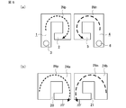
- FIG. 2 is a plan view for explaining the winding pattern of the first embodiment.
- the winding patterns 1, 7, and 13 constituting the winding patterns on the positive electrode side of the second layer, the third layer, and the fourth layer arranged as shown in FIG.
- the respective winding patterns 4, 10, and 16 constituting the line pattern are shown. That is, FIG. 2A shows a winding pattern on the second layer positive electrode side and a winding pattern on the second layer negative electrode side.
- FIG. 2B shows a winding pattern on the third layer positive electrode side and a winding pattern on the third layer negative electrode side.
- FIG. 2C shows a winding pattern on the fourth layer positive electrode side and a winding pattern on the fourth layer negative electrode side.
- Each of the winding patterns is provided with a positive side winding pattern input terminal 3, a negative side winding pattern input terminal 6, a positive side winding pattern output terminal 14, and a negative side winding pattern output terminal 18. ing. Between the winding pattern between the second layer and third layer terminals (also referred to as connection positions) 2 and end 8 or between end 5 and end 12, between the third and fourth layer terminals The end 9 and the end 15 and the end 11 and the end 17 are electrically connected by, for example, an inner via hole (IVH). At this time, since the heat generation at the via position increases as the current density in the via portion increases, it is desirable that the via has a plurality of vias having a cross-sectional area comparable to that of the winding pattern.
- the winding patterns 1 and 4 and the winding patterns 13 and 16 are formed with slits 25 and 26 and slits 27 and 28, respectively.
- FIG. 3 is a plan view for explaining the ground pattern of the first embodiment.
- FIG. 3A shows a positive-side ground pattern 24a and a negative-side ground pattern 24b constituting the first-layer ground pattern
- FIG. 3B shows a positive-side ground constituting the fifth-layer ground pattern.
- a pattern 19a and a ground pattern 19b on the negative electrode side are shown, and a ground capacitor is formed between the second layer and the fourth layer, respectively. Since the capacitance of the capacitor is proportional to the area of the opposing conductor, in order to form as large a capacitance as possible, the ground patterns 24a, 24b, and 19a are located at positions that completely face the winding patterns 1, 4, 13, and 16. , 19b provides the maximum facing area and the maximum capacitance.
- the ground patterns 24a and 24b and the ground patterns 19a and 19b are extended and arranged outside the winding pattern at positions 29, 30, 31, and 32 facing the input terminals 3 and 6 and the output terminals 14 and 18 of the winding pattern. It is installed.
- the ground patterns 24 a and 24 b are arranged to have a larger area than the opposing winding patterns 1 and 4.
- the ground patterns 24a and 24b and the ground patterns 19a and 19b are provided with slits 20 and 21 and slits 22 and 23, respectively.
- this slit is not formed, when the ground pattern is conducted around the magnetic core, the high frequency impedance of the winding is short-circuited due to magnetic coupling with the winding of the winding pattern, and the magnetic core Although the effect of high impedance at high frequency with winding is lost, such a problem does not occur by providing this slit.
- the second layer positive electrode side and negative electrode side winding pattern is the first layer ground pattern
- the fourth layer positive electrode side and negative electrode side winding pattern is the fifth layer ground pattern
- a capacitance (ground capacitor) is formed between them. Since the ground capacitor has a small impedance to the common mode high-frequency noise current, the noise current can be passed through the ground layer and only the noise current can be attenuated. Since the dielectric layer between the winding pattern and the ground layer for forming the capacitance has a higher dielectric constant or a smaller thickness, the capacitance increases and the noise attenuation effect increases.
- both the positive electrode side and negative electrode side winding patterns are wound around a magnetic core 400 having a high relative permeability at a high frequency such as a ferrite core, an amorphous core, or a crystalline metal magnetic core. Since the direction of the magnetic flux that links the cores of the common mode noise current flowing through both the positive and negative windings is the same, it is effective in attenuating the common mode noise flowing through the positive and negative electrodes.
- the magnetic core in the first embodiment is a combination of two U-shaped cores (also referred to as a UU core), or a combination of two types of U-shaped and I-shaped cores (also referred to as a UI core). However, as described in the third embodiment described later, a combination of two E-shaped cores (also referred to as an EE core), or a combination of two types of E-shaped and I-shaped cores ( (Also referred to as EI core).
- FIG. 4 is a diagram simply showing noise current paths of the positive electrode and the negative electrode flowing from the second winding pattern to the first ground pattern in the first embodiment.
- FIG. 4A shows a winding pattern on the second layer positive electrode side and a winding pattern on the second layer negative electrode side.
- FIG. 4B shows a ground pattern on the positive electrode side and a ground pattern on the negative electrode side constituting the ground pattern of the first layer.
- the ground patterns 24a and 24b are provided with slits 20 and 21 so that the pattern around the magnetic core 400 does not conduct, the ground potential passes through the forward path and the ground pattern flowing through the winding pattern.
- the slits 20 and 21 of the ground patterns 24a and 24b shown in FIG. 4 are positioned so as to overlap with the slits 25 and 26 of the winding patterns 1 and 4 facing each other through a dielectric.
- the condition in which the slits of the pattern and slits of the winding pattern overlap so that the capacitance is maximized is the largest condition, and the attenuation effect of the common mode noise filter is the greatest.
- the relationship between the slit position and the filter attenuation effect is the same for the slits 22 and 23 of the ground patterns 19a and 19b on the output side and the slits 27 and 28 of the winding patterns 13 and 16.
- FIG. 5A shows a winding pattern on the second layer positive electrode side and a winding pattern on the second layer negative electrode side.
- FIG. 5B shows a ground pattern on the positive electrode side and a ground pattern on the negative electrode side constituting the ground pattern of the first layer.
- FIG. 8A shows a winding pattern on the second layer positive electrode side and a winding pattern on the second layer negative electrode side.
- FIG. 8B shows a ground pattern on the positive electrode side and a ground pattern on the negative electrode side constituting the ground pattern of the first layer.
- FIG. 9A shows a winding pattern on the second layer positive electrode side and a winding pattern on the second layer negative electrode side.
- FIG. 9B shows a ground pattern on the positive electrode side and a ground pattern on the negative electrode side constituting the ground pattern of the first layer.
- FIGS. 10 and 11 are perspective views illustrating the grounding structure of the ground pattern according to the first embodiment.
- the power converter energy lost in the power semiconductor portion is generated as heat. Furthermore, since a large current of several tens to several hundreds of A flows in the winding in order to transmit a larger amount of power, the power converter generates a large amount of heat from the winding wiring. For this reason, the power conversion device often attaches the heat radiation fin 800 to the noise filter. On the other hand, the radiating fin 800 is used as a ground potential because it is a metal block.
- the radiating fin is used as a ground for cooling the noise filter and grounding the ground capacitor.
- the heat radiating fin 800 is provided with a groove (recessed portion) 801.
- the noise filter is attached as shown in FIGS. 10 and 11, the lower portion of the magnetic core 400 is fitted into the groove 801 and accommodated. Then, the ground pattern of the ground conductor 19 and the radiating fin 800 come into contact with each other.
- This noise filter is attached to the radiating fin 800 with a conductive screw 600 with low contact resistance with a conductor spacer 500 interposed between the ground conductor 19 and the ground conductor 24.
- the ground conductor 24 is also coupled together and grounded.
- the heat dissipating fin 800 is insulated.
- the ground pattern is extended and disposed outside the winding pattern at the input / output terminal position, and the ground pattern is not a line but a planar pattern. Can be grounded with small self-inductance.
- the self-resonant frequency is 50 MHz or more, that is, the noise attenuation effect is exhibited even if it is 50 MHz or more.
- a common mode noise filter can be realized.
- the common mode noise filter according to the first embodiment has a substrate structure, heat is easily transmitted in a direction perpendicular to the surface of the substrate, and the ground pattern is wide. I can tell you. As a result, the cross-sectional area of the winding pattern constituting the common mode noise filter can be reduced, and there is no need for a separate member that dissipates the Joule heat of the winding pattern.
- the configuration in which the winding is wound from the outside reduces the wiring inductance of the capacitor as compared to starting winding from the inside as shown in FIG. 8, so the wiring inductance of the capacitor is reduced. Can be maintained.
- the number of pattern layers when realizing the same number of patterns is smaller than winding the winding from the outside, and as a result, the total length of the winding pattern is shortened.
- the calorific value can be kept small.
- the outside described here indicates the outer peripheral side (outside) of the common mode magnetic flux that forms a closed magnetic path in the magnetic body in the UU core or UI core.
- the substrate-type winding pattern is a single phase.
- the present invention is not limited to this, and the same configuration can be achieved even in the case of a three-phase, and the winding patterns are magnetically coupled. Thus, similar effects can be obtained.
- FIG. FIG. 12 is a perspective view for explaining the common mode noise filter according to the second embodiment.
- the noise filter of the second embodiment is a two-stage noise filter 900 configured using two noise filters (common mode noise filters) 700 shown in the first embodiment. By using two stages, the noise attenuation effect is greatly improved.
- the ground pattern is extended and disposed outside the winding pattern at the input / output terminal position, as in the first embodiment.
- the common mode noise filter of the second embodiment is a substrate type that forms a winding conductor and a ground conductor by a pattern, a winding pattern and a ground pattern of a two-stage filter can be created integrally.
- the grounding area does not increase by the amount of terminal connection and is small.
- FIG. 14 is a perspective view of the noise filter according to the third embodiment, and shows a state in which the radiation fins 1800 are attached.
- FIG. 15 is a cross-sectional view taken along line BB of the common mode noise filter shown in FIG. The ground pattern is extended and disposed outside the winding pattern at the input / output terminal position, as in the first embodiment.
- a noise filter (common mode noise filter) 1700 shown in FIG. 14 is roughly similar to the first embodiment in winding conductor 1100 (see FIGS. 16 and 17) constituting the winding pattern, winding conductor. It is composed of a dielectric (also referred to as dielectric resin) 1200 that insulates between them, a ground conductor that constitutes ground patterns 119 and 124, and a magnetic core 1400.
- the radiating fin 1800 is provided with a groove, and the lower portion of the magnetic core 1400 is fitted and accommodated in the groove.
- this noise filter is attached to heat radiating fin 1800 by conductive screw 1600, and the mounting structure is the same as the mounting structure of the noise filter and heat radiating fin by conductive screw 600 in the first embodiment. Yes.
- the magnetic core 1400 has a structure in which two E-shaped cores (E-shaped core) are combined, or an E-shaped core and an I-shaped core (I-shaped core) are combined.
- the winding conductor 1100 is a winding made of a planar conductor.
- the winding has a substrate structure, and a dielectric resin 1200 (see FIG. 15) for insulation is sandwiched between the windings. Further, the edge surface of the conductor is also covered with a dielectric resin in order to enhance insulation.
- the winding is wound for two turns, and the two-turn winding is composed of three conductor layers on each of the positive electrode side and the negative electrode side. Constitutes the ground layer.
- an E-type core is used as the magnetic core 1400 and the positions of the winding pattern on the positive side and the negative side will be described.
- FIGS. 16A to 16C show the winding patterns 101, 107, and 113 constituting the winding pattern on the positive electrode side of the second, third, and fourth layers.
- 17A to 17C show the winding patterns 116, 110, and 104 constituting the winding patterns on the negative electrode side of the fifth layer, the sixth layer, and the seventh layer, respectively.
- the second to seventh winding patterns are formed in the order of the winding patterns 101, 107, 113, 116, 110, and 104.
- Each of the winding patterns is provided with a positive side winding pattern input terminal 103, a negative side winding pattern input terminal 106, a positive side winding pattern output terminal 114, and a negative side winding pattern output terminal 118.
- the end portion 117 and the end portion 112 between the terminals of the fifth and sixth layers and the terminal portion 111 and the end portion 105 between the terminals of the sixth layer and the seventh layer are, for example, inner via holes (IVH). Electrically connected.
- IVH inner via holes
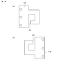
- FIG. 18 is a plan view of the ground pattern of the noise filter according to the third embodiment.
- 18A shows the ground pattern 124 of the first layer
- FIG. 18B shows the ground pattern 119 of the seventh layer.
- a ground capacitor is formed between the second layer and the sixth layer, respectively. To do. It is necessary to provide slits 120 and 122 in the ground patterns 124 and 119 as in the first embodiment.
- the grounding position of the ground layer is also the noise current (outward path noise current) flowing through the winding pattern and the noise current (flowing to the ground potential through the ground pattern) ( It is necessary to ground so that the direction of the noise current on the return path is opposite.
- the ground layer is provided at one location on the positive electrode side and one on the negative electrode side.
- FIG. 19 is a cross-sectional view of a common mode filter that is a noise filter according to the fourth embodiment.
- the cross-sectional position corresponds to the line BB in FIG. 14 showing the third embodiment.
- the positive winding 127 and the negative winding 128 are insulated by an insulating spacer 129.
- 20A and 20B are plan views of the winding pattern of the noise filter according to the fourth embodiment.
- FIG. 20A shows the positive electrode side
- FIG. 20B shows the negative electrode side.
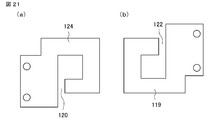
- FIG. 21 is a plan view of the ground pattern of the noise filter according to the fourth embodiment.
- FIG. 21A shows the positive electrode side
- FIG. 21B shows the negative electrode side.
- the ground pattern is extended and disposed outside the winding pattern at the input / output terminal position, as in the first embodiment.
- the ground pattern 124 on the positive electrode side and the winding pattern 101 for forming a capacitor between the ground and the ground are integrated as a substrate, for example, and a large capacitance is realized by using a dielectric between the ground pattern and the winding pattern. ing. The same applies to the capacitor on the negative electrode side.
- the configuration of the part forming the capacitor is the same as that of the third embodiment.
- the windings 127 and 128 other than the portion constituting the capacitor are not formed in the pattern as in the third embodiment but are formed in a spiral shape, for example.
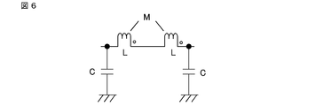
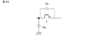
- the winding that does not face the ground pattern of the winding conductor is not a substrate pattern, but is formed of a continuous conductor, so that the dielectric does not enter between windings of the same polarity, thus reducing the capacitance between the windings. It becomes possible to do. Since the capacitance (parasitic capacitance) Cs between windings of the same polarity is parallel to the inductance (common mode inductance) L as shown in the equivalent circuit of FIG.
- the noise reduction of the noise filter is reduced as the capacitance Cs is smaller. Performance is improved.
- the relationship with the ground-to-ground capacitor Cg is expressed as shown in FIG.
- the winding patterns 101 and 104 forming the ground-to-ground capacitor Cg and the windings 127 and 128 are connected to each other at the connection positions 125 and 126 by screwing, welding, or the like.
- FIG. 23 is a perspective view of the noise filter 2000 of the fifth embodiment, and shows a state in which the radiation fins 3800 are attached. Similar to the fourth embodiment, the winding conductor is formed in a spiral shape, and since no dielectric is contained between the windings of the same polarity, the capacitance between the windings can be reduced. For this reason, the capacitance in parallel with the inductance formed by the winding and the magnetic core is small, and the noise reduction performance is improved.
- FIG. 24 is a perspective view of the capacitor member 2100 and the capacitor member 2200 constituting the capacitor of the noise filter of the fifth embodiment.
- FIG. 24A shows a capacitor member 2100 on the positive electrode side
- FIG. 24B shows a capacitor member on the negative electrode side.
- FIG. 25 is a diagram showing a winding pattern and a ground pattern of the capacitor member 2100 and the capacitor member 2200 that constitute the capacitor of the fifth embodiment.
- FIG. 25A shows a winding pattern 2201 on the positive electrode side and a ground pattern on the positive electrode side
- FIG. 25B shows a winding pattern on the negative electrode side and a ground pattern on the negative electrode side.
- the ground patterns 2104 and 2204 are extended and disposed outside the winding pattern at the input / output terminal positions 2103 and 2203, and further, slits 2105 and 2205 are formed. It is.
- the dielectric resin is sandwiched between the winding patterns 2201, 2101 and the ground patterns 2204, 2104, and a capacitor is formed between the winding pattern and the ground pattern to have a function of reducing noise. Same as 1.
- the fifth embodiment is characterized in that the ground pattern is bent, unlike the first to fourth embodiments.
- FIG. 26 shows a winding conductor formed in a spiral shape according to the fifth embodiment.
- FIG. 26A shows a winding conductor 2800 on the positive electrode side
- FIG. 26B shows a winding conductor on the negative electrode side.
- FIG. The terminal portion 2701 and the terminal portion 2801 are electrically connected to the input / output terminal positions 2202 and 2102 having the pattern shown in FIG. 25 by screwing, welding, or the like.
- FIG. 27 is a cross-sectional view taken along the cutting line (CC arrow) shown in FIG.
- a metal pressing member 2300 for pressing the magnetic core 2400 against the radiating fin 3800 is provided.
- the winding conductor 2800 is pressed against the radiating fin 3800 by, for example, screwing or the like, through the insulating sheet 2500 having high thermal conductivity, the magnetic core 2400, and the insulating spacer 3000.
- the side surface of the winding conductor 2700 is pressed against the insulating sheet 3100 having high thermal conductivity.
- the capacitor members 2100 and 2200 that use a dielectric to form a capacitor between the winding pattern and the ground pattern not only propagate the noise current but also propagate heat to the heat radiation fins. Since it becomes a route, heat dissipation is excellent. For this reason, the cross-sectional area of the winding conductor can be reduced, and as a result, the magnetic core can be reduced, so that the entire filter can be reduced in size.
- heat is propagated to the metal member 2900 connected to the heat radiating fin through the insulating sheet 3100 having a high thermoelectric property on the side surface of the winding conductor, thereby improving the heat dissipation of the filter.
- the whole can be downsized.
- the magnetic core is of a type having high electrical conductivity
- the winding conductor 2700 is pressed directly against the insulating sheet 3100 with the magnetic core, a noise current flows from the winding to the magnetic core and bypasses the noise filter.
- the reason why the insulating sheet 3100 is insulative is also the same.
- the insulating spacer 3000 has a configuration in which an insulating member and a spring are combined, the winding conductor can be pressed against the insulating sheet 3100 using elastic force, so that an allowable winding and ferrite core dimensional error is also large. Therefore, the manufacturing cost can be reduced.
- a magnetic core generally has a property that its characteristics change with temperature.
- the pressing member 2300 for pressing the magnetic core is made of metal. The method of propagating heat from the side surface of the winding conductor described in the fifth embodiment to the heat radiating fin is also effective in the noise filter of the first embodiment covered with an insulator.
- the embodiments can be freely combined within the scope of the invention, and the embodiments can be appropriately modified or omitted.
Abstract
Description
図1は、実施の形態1に係るノイズフィルタ(コモンモードノイズフィルタとも称す)を説明するための斜視図、図13は図1に示すコモンモードノイズフィルタのA-A線における断面図である。
FIG. 1 is a perspective view for explaining a noise filter (also referred to as a common mode noise filter) according to
グラウンドパターン24a、24bとグラウンドパターン19a、19bが巻線パターンの入力端子3、6および出力端子14、18に対向する位置29、30、31、32において、巻線パターンの外側に延伸されて配設されている。言い換えると、例えば、グラウンドパターン24a、24bは、それぞれ対向する巻線パターン1、4よりも面積が広く配置されていることになる。
また、グラウンドパターン24a、24bとグラウンドパターン19a、19bは、それぞれスリット20、21とスリット22、23が形成されている。本スリットが形成されていなければ、磁性体コアの周りでグラウンドパターンが導通すると巻線パターンの巻線との磁気結合により、巻線の高周波インピーダンスがショートした状態のようになり、磁性体コアに巻線を施した高周波での高いインピーダンスの効果が失われてしまうが、本スリットを設けることによりこのような問題を生じない。 FIG. 3 is a plan view for explaining the ground pattern of the first embodiment. FIG. 3A shows a positive-
The
The
このような場合は、図7の等価回路となり、ノイズ減衰効果は図6に比べて著しく低い。内側から巻き始める巻線パターンの場合でも、同様に考える必要があり、図8のように接地させると、等価回路は図6のようになるが、図9のように接地させると、等価回路は、図7のようになるため、図8のように接地させる方が図9のように接地させるよりノイズ減衰効果は高い。なお、上記メカニズムは4層目の巻線パターンと5層目のグラウンドパターンの関係にも当てはまる。なお、図8(a)は2層目正極側の巻線パターンと2層目負極側の巻線パターンを示している。図8(b)は1層目のグラウンドパターンを構成する正極側のグラウンドパターンと負極側のグラウンドパターンを示している。また、図9(a)は2層目正極側の巻線パターンと2層目負極側の巻線パターンを示している。図9(b)は1層目のグラウンドパターンを構成する正極側のグラウンドパターンと負極側のグラウンドパターンを示している。 On the other hand, if the ground pattern is grounded as shown in FIG. 5, the noise current flows to the ground potential only in the forward path, so the generated magnetic flux interlinks the core, and the winding pattern has two turns. Will be coupled with the inductance. FIG. 5A shows a winding pattern on the second layer positive electrode side and a winding pattern on the second layer negative electrode side. FIG. 5B shows a ground pattern on the positive electrode side and a ground pattern on the negative electrode side constituting the ground pattern of the first layer.
In such a case, the equivalent circuit of FIG. 7 is obtained, and the noise attenuation effect is significantly lower than that of FIG. Even in the case of a winding pattern that starts winding from the inside, it is necessary to think in the same way. When grounded as shown in FIG. 8, the equivalent circuit is as shown in FIG. 6, but when grounded as shown in FIG. 7, the noise attenuation effect is higher when grounding as shown in FIG. 8 than when grounding as shown in FIG. The above mechanism also applies to the relationship between the fourth layer winding pattern and the fifth layer ground pattern. FIG. 8A shows a winding pattern on the second layer positive electrode side and a winding pattern on the second layer negative electrode side. FIG. 8B shows a ground pattern on the positive electrode side and a ground pattern on the negative electrode side constituting the ground pattern of the first layer. FIG. 9A shows a winding pattern on the second layer positive electrode side and a winding pattern on the second layer negative electrode side. FIG. 9B shows a ground pattern on the positive electrode side and a ground pattern on the negative electrode side constituting the ground pattern of the first layer.
また、実施の形態1では、基板型巻線パターンが単相の場合を記載したが、これに限らず、三相の場合でも同様に構成することができ、巻線パターンどうしが磁気的に結合しており、同様の作用効果を得ることができる。 In the first embodiment, a description is given of a pattern in which the winding starts to be wound from the outside as shown in FIG. The configuration in which the winding is wound from the outside reduces the wiring inductance of the capacitor as compared to starting winding from the inside as shown in FIG. 8, so the wiring inductance of the capacitor is reduced. Can be maintained. On the other hand, when winding is started from the inside, the number of pattern layers when realizing the same number of patterns is smaller than winding the winding from the outside, and as a result, the total length of the winding pattern is shortened. The calorific value can be kept small. The outside described here indicates the outer peripheral side (outside) of the common mode magnetic flux that forms a closed magnetic path in the magnetic body in the UU core or UI core.
In the first embodiment, the case where the substrate-type winding pattern is a single phase has been described. However, the present invention is not limited to this, and the same configuration can be achieved even in the case of a three-phase, and the winding patterns are magnetically coupled. Thus, similar effects can be obtained.
図12は、実施の形態2に係るコモンモードノイズフィルタを説明するための斜視図である。実施の形態2のノイズフィルタは、実施の形態1で示したノイズフィルタ(コモンモードノイズフィルタ)700を2個用いて構成した2段ノイズフィルタ900である。2段にすることで、ノイズ減衰効果が大幅に向上する。グラウンドパターンが入出力端子位置において、巻線パターンの外側に延伸されて配設されていることは、実施の形態1と同様である。
FIG. 12 is a perspective view for explaining the common mode noise filter according to the second embodiment. The noise filter of the second embodiment is a two-
それに対して、本実施の形態2のコモンモードノイズフィルタは、パターンで巻線導体、グラウンド導体を構成する基板型であるので、2段のフィルタの巻線パターン、グラウンドパターンを一体で作成できるため接地面積が端子接続分増えることはなく小型である。 Furthermore, in the case of a conventional common mode noise filter configured by combining an inductor and a capacitor of individual components, it is necessary to provide a new terminal in order to electrically connect the two inductors and the inductor and the capacitor. Is simply larger than the sum of the individual parts constituting the filter.
On the other hand, since the common mode noise filter of the second embodiment is a substrate type that forms a winding conductor and a ground conductor by a pattern, a winding pattern and a ground pattern of a two-stage filter can be created integrally. The grounding area does not increase by the amount of terminal connection and is small.
図14は、実施の形態3に係るノイズフィルタの斜視図であって、放熱フィン1800を取り付けた状態を示している。図15は、図14に示すコモンモードノイズフィルタのB-B線における断面図である。グラウンドパターンが入出力端子位置において、巻線パターンの外側に延伸されて配設されていることは、実施の形態1と同様である。
FIG. 14 is a perspective view of the noise filter according to the third embodiment, and shows a state in which the
放熱フィン1800には、実施の形態1と同様に溝が設けられており、この溝に磁性体コア1400の下部が嵌まり込んで収容されている。また、導電性ねじ1600によって本ノイズフィルタが放熱フィン1800に取り付けられており、その取付構造は、実施の形態1における導電性ねじ600によるノイズフィルタと放熱フィンとの取付構造と同様に構成されている。 A noise filter (common mode noise filter) 1700 shown in FIG. 14 is roughly similar to the first embodiment in winding conductor 1100 (see FIGS. 16 and 17) constituting the winding pattern, winding conductor. It is composed of a dielectric (also referred to as dielectric resin) 1200 that insulates between them, a ground conductor that constitutes
As in the first embodiment, the radiating
図19は、実施の形態4に係るノイズフィルタであるコモンモードフィルタの断面図である。断面位置は、実施の形態3を示している図14におけるB-B線に相当するところである。正極側の巻線127と負極側の巻線128は、絶縁体製のスペーサ129で絶縁されている。
図20は、本実施の形態4に係るノイズフィルタの巻線パターンの平面図であって、図20(a)は正極側、図20(b)は負極側を表わしている。図21は本実施の形態4に係るノイズフィルタのグラウンドパターンの平面図であって、図21(a)は正極側、図21(b)は負極側を表わしている。
グラウンドパターンが入出力端子位置において、巻線パターンの外側に延伸されて配設されていることは、実施の形態1と同様である。
FIG. 19 is a cross-sectional view of a common mode filter that is a noise filter according to the fourth embodiment. The cross-sectional position corresponds to the line BB in FIG. 14 showing the third embodiment. The positive winding 127 and the negative winding 128 are insulated by an insulating
20A and 20B are plan views of the winding pattern of the noise filter according to the fourth embodiment. FIG. 20A shows the positive electrode side, and FIG. 20B shows the negative electrode side. FIG. 21 is a plan view of the ground pattern of the noise filter according to the fourth embodiment. FIG. 21A shows the positive electrode side, and FIG. 21B shows the negative electrode side.
The ground pattern is extended and disposed outside the winding pattern at the input / output terminal position, as in the first embodiment.
図25は、本実施の形態5のコンデンサを構成するコンデンサ部材2100とコンデンサ部材2200の巻線パターンとグラウンドパターンを示した図である。図25(a)は、正極側の巻線パターン2201と正極側のグラウンドパターンを、図25(b)は、負極側の巻線パターンと負極側のグラウンドパターンを示している。グラウンドパターン2104、2204が入出力端子位置2103、2203において、巻線パターンの外側に延伸されて配設されており、さらに、スリット2105、2205が形成されていることは、実施の形態1と同様である。巻線パターン2201、2101とグラウンドパターン2204、2104の間に誘電体樹脂が挟まれており、巻線パターンとグラウンドパターンの間にコンデンサを形成し、ノイズを低減する機能を有することも実施の形態1と同様である。本実施の形態5は、実施の形態1~4と異なりグラウンドパターンを折り曲げてあることが特徴である。 FIG. 24 is a perspective view of the
FIG. 25 is a diagram showing a winding pattern and a ground pattern of the
Claims (12)
- 平面状の導体からなり、層状に配置され層間を電気的に接続した巻線パターンを構成する巻線導体と、前記巻線パターンの導体との間に誘電体を挟んで配置されグラウンドパターンを構成するグラウンド導体と、前記巻線パターンが巻き回された磁性体コアを備えたノイズフィルタであって、前記グラウンドパターンが巻線パターンの入出力端子に対向する位置において、巻線パターンの外側に延伸されて配設されており、前記グラウンド導体のグラウンドパターンには、前記磁性体コアの周りに配置される部分を分断するスリットが設けられていることを特徴とするノイズフィルタ。 It is composed of a planar conductor, and a ground pattern is formed by placing a dielectric between the winding conductor that forms a winding pattern that is arranged in layers and electrically connected between the layers, and the conductor of the winding pattern. A noise filter including a ground conductor and a magnetic core around which the winding pattern is wound, wherein the ground pattern extends outside the winding pattern at a position facing the input / output terminal of the winding pattern. The noise filter is characterized in that the ground pattern of the ground conductor is provided with a slit for dividing a portion disposed around the magnetic core.
- 前記巻線導体の入出力端子が前記磁性体コアのコア内で閉磁路を形成する磁束の外周側に設けられていることを特徴とする請求項1に記載のノイズフィルタ。 2. The noise filter according to claim 1, wherein an input / output terminal of the winding conductor is provided on an outer peripheral side of a magnetic flux forming a closed magnetic path in the core of the magnetic core.
- 前記巻線導体は、基板状に前記巻線パターンが形成され、前記巻線パターンが複数相設けられており、前記巻線パターンどうしが磁気的に結合していることを特徴とする請求項1に記載のノイズフィルタ。 2. The winding conductor according to claim 1, wherein the winding pattern is formed in a substrate shape, the winding patterns are provided in a plurality of phases, and the winding patterns are magnetically coupled to each other. The noise filter described in 1.
- 前記グラウンド導体のグラウンドパターンに設けられた前記スリットの位置と前記誘電体を介して対向する前記巻線導体の巻線パターンに設けられたスリットの位置が重なりあうように前記グラウンドパターンと前記巻線パターンが配置されていることを特徴とする請求項1に記載のノイズフィルタ。 The ground pattern and the winding so that the position of the slit provided in the ground pattern of the ground conductor and the position of the slit provided in the winding pattern of the winding conductor facing each other through the dielectric overlap each other. The noise filter according to claim 1, wherein a pattern is arranged.
- 前記グラウンド導体の前記グラウンドパターンに接続された放熱フィンを備えたことを特徴とする請求項1に記載のノイズフィルタ。 The noise filter according to claim 1, further comprising a radiation fin connected to the ground pattern of the ground conductor.
- 前記放熱フィンには、前記磁性体コアを収容する溝が設けられ、前記磁性体コアが前記溝に収納された状態で前記グラウンド導体のグラウンドパターンが前記放熱フィンに接続されたことを特徴とする請求項5に記載されたノイズフィルタ。 The heat radiation fin is provided with a groove for accommodating the magnetic core, and a ground pattern of the ground conductor is connected to the heat radiation fin in a state where the magnetic core is accommodated in the groove. The noise filter according to claim 5.
- 前記巻線導体の前記グラウンドパターンと対向しない巻線が一続きの線で形成されていることを特徴とする請求項1に記載のノイズフィルタ。 The noise filter according to claim 1, wherein the winding of the winding conductor that is not opposed to the ground pattern is formed by a continuous line.
- 前記ノイズフィルタが複数組直列接続されたことを特徴とする請求項1に記載のノイズフィルタ。 The noise filter according to claim 1, wherein a plurality of the noise filters are connected in series.
- 前記巻線導体の側面と放熱フィンが絶縁物を介して接していることを特徴とする請求項7に記載のノイズフィルタ。 The noise filter according to claim 7, wherein a side surface of the winding conductor and the heat dissipating fin are in contact with each other through an insulator.
- 前記磁性体コアを前記放熱フィンに押えつける押え部材を備えたことを特徴とする請求項9に記載のノイズフィルタ。 The noise filter according to claim 9, further comprising a pressing member that presses the magnetic core against the radiating fin.
- 前記巻線導体と前記磁性体コアの間に絶縁性部材を備えていることを特徴とする請求項10に記載のノイズフィルタ。 The noise filter according to claim 10, further comprising an insulating member between the winding conductor and the magnetic core.
- 前記誘電体と放熱フィンが接していることを特徴とする請求項1に記載のノイズフィルタ。 The noise filter according to claim 1, wherein the dielectric and the radiating fin are in contact with each other.
Priority Applications (4)
| Application Number | Priority Date | Filing Date | Title |
|---|---|---|---|
| EP15884691.5A EP3270511A4 (en) | 2015-03-11 | 2015-12-04 | Noise filter |
| US15/554,159 US20180053591A1 (en) | 2015-03-11 | 2015-12-04 | Noise filter |
| JP2016515555A JP5951163B1 (en) | 2015-03-11 | 2015-12-04 | Noise filter |
| CN201580077567.1A CN107431469A (en) | 2015-03-11 | 2015-12-04 | Noise filter |
Applications Claiming Priority (4)
| Application Number | Priority Date | Filing Date | Title |
|---|---|---|---|
| JP2015-047908 | 2015-03-11 | ||
| JP2015047908 | 2015-03-11 | ||
| PCT/JP2015/063552 WO2016143149A1 (en) | 2015-03-11 | 2015-05-12 | Noise filter |
| JPPCT/JP2015/063552 | 2015-05-12 |
Publications (1)
| Publication Number | Publication Date |
|---|---|
| WO2016143207A1 true WO2016143207A1 (en) | 2016-09-15 |
Family
ID=56878586
Family Applications (1)
| Application Number | Title | Priority Date | Filing Date |
|---|---|---|---|
| PCT/JP2015/084152 WO2016143207A1 (en) | 2015-03-11 | 2015-12-04 | Noise filter |
Country Status (1)
| Country | Link |
|---|---|
| WO (1) | WO2016143207A1 (en) |
Cited By (1)
| Publication number | Priority date | Publication date | Assignee | Title |
|---|---|---|---|---|
| JP2020194884A (en) * | 2019-05-28 | 2020-12-03 | 株式会社豊田自動織機 | Transformer structure |
Citations (4)
| Publication number | Priority date | Publication date | Assignee | Title |
|---|---|---|---|---|
| JPH05234811A (en) * | 1992-02-24 | 1993-09-10 | Toho Aen Kk | Surface mount lc noise filter and manufacture thereof |
| JP2000252124A (en) * | 1999-02-24 | 2000-09-14 | Kankyo Denji Gijutsu Kenkyusho:Kk | Common mode filter |
| US6384705B1 (en) * | 1999-12-30 | 2002-05-07 | Industrial Technology Research Institute | Multilayer-type chip common mode filter |
| JP2004200826A (en) * | 2002-12-17 | 2004-07-15 | Hioki Ee Corp | Distributed constant filter element |
-
2015
- 2015-12-04 WO PCT/JP2015/084152 patent/WO2016143207A1/en active Application Filing
Patent Citations (4)
| Publication number | Priority date | Publication date | Assignee | Title |
|---|---|---|---|---|
| JPH05234811A (en) * | 1992-02-24 | 1993-09-10 | Toho Aen Kk | Surface mount lc noise filter and manufacture thereof |
| JP2000252124A (en) * | 1999-02-24 | 2000-09-14 | Kankyo Denji Gijutsu Kenkyusho:Kk | Common mode filter |
| US6384705B1 (en) * | 1999-12-30 | 2002-05-07 | Industrial Technology Research Institute | Multilayer-type chip common mode filter |
| JP2004200826A (en) * | 2002-12-17 | 2004-07-15 | Hioki Ee Corp | Distributed constant filter element |
Non-Patent Citations (1)
| Title |
|---|
| See also references of EP3270511A4 * |
Cited By (1)
| Publication number | Priority date | Publication date | Assignee | Title |
|---|---|---|---|---|
| JP2020194884A (en) * | 2019-05-28 | 2020-12-03 | 株式会社豊田自動織機 | Transformer structure |
Similar Documents
| Publication | Publication Date | Title |
|---|---|---|
| US10366826B2 (en) | Dual-mode choke coil and high-frequency filter using same, and on-board motor integrated electric power steering and on-board charging device | |
| US10491180B2 (en) | Board-type noise filter and electronic device | |
| US7642891B2 (en) | Planar inductance | |
| US8964410B2 (en) | Transformer with externally-mounted rectifying circuit board | |
| US20130027170A1 (en) | Isolated power converter with magnetics on chip | |
| TWI584310B (en) | Shield for toroidal core electromagnetic device, and toroidal core electromagnetic devices utilizing such shields | |
| WO2016143149A1 (en) | Noise filter | |
| CN112425072A (en) | Noise filter | |
| WO2018012059A1 (en) | Compound smoothing inductor and smoothing circuit | |
| WO2016143207A1 (en) | Noise filter | |
| JP3823322B2 (en) | Distributed constant structure | |
| JP5951163B1 (en) | Noise filter | |
| CN107768122B (en) | Coupled inductor for low electromagnetic interference | |
| JP6210464B2 (en) | electric circuit | |
| JP2013038935A (en) | Common-mode choke coil | |
| JP6344540B2 (en) | Power conversion module | |
| JP2012099512A (en) | Composite electronic component | |
| JP4854923B2 (en) | Magnetic coupling element | |
| JP6823130B2 (en) | Filter device | |
| CN213071122U (en) | Shielding structure and semiconductor device | |
| JP6676888B2 (en) | Power converter | |
| WO2022049695A1 (en) | Connection structure | |
| JP2019179904A (en) | Coil unit, wireless power transmission device, wireless power reception device, and wireless power transmission system | |
| JP2016213344A (en) | Noise suppressing component | |
| WO2023013343A1 (en) | Switching power supply device |
Legal Events
| Date | Code | Title | Description |
|---|---|---|---|
| ENP | Entry into the national phase |
Ref document number: 2016515555 Country of ref document: JP Kind code of ref document: A |
|
| 121 | Ep: the epo has been informed by wipo that ep was designated in this application |
Ref document number: 15884691 Country of ref document: EP Kind code of ref document: A1 |
|
| WWE | Wipo information: entry into national phase |
Ref document number: 15554159 Country of ref document: US |
|
| REEP | Request for entry into the european phase |
Ref document number: 2015884691 Country of ref document: EP |
|
| NENP | Non-entry into the national phase |
Ref country code: DE |