WO2016113936A1 - 画像補正装置、撮像装置、及び、補正テーブル作成方法 - Google Patents
画像補正装置、撮像装置、及び、補正テーブル作成方法 Download PDFInfo
- Publication number
- WO2016113936A1 WO2016113936A1 PCT/JP2015/071525 JP2015071525W WO2016113936A1 WO 2016113936 A1 WO2016113936 A1 WO 2016113936A1 JP 2015071525 W JP2015071525 W JP 2015071525W WO 2016113936 A1 WO2016113936 A1 WO 2016113936A1
- Authority
- WO
- WIPO (PCT)
- Prior art keywords
- pixel
- data
- correction
- imaging
- image sensor
- Prior art date
- Legal status (The legal status is an assumption and is not a legal conclusion. Google has not performed a legal analysis and makes no representation as to the accuracy of the status listed.)
- Ceased
Links
Images






Classifications
-
- H—ELECTRICITY
- H04—ELECTRIC COMMUNICATION TECHNIQUE
- H04N—PICTORIAL COMMUNICATION, e.g. TELEVISION
- H04N25/00—Circuitry of solid-state image sensors [SSIS]; Control thereof
- H04N25/60—Noise processing, e.g. detecting, correcting, reducing or removing noise
- H04N25/68—Noise processing, e.g. detecting, correcting, reducing or removing noise applied to defects
Definitions
- the present invention relates to an image correction apparatus, an imaging apparatus, and a correction table creation method.
- Patent Document 1 by the present applicant proposes a technique for improving SNR [signal-to-noise ratio] by forming an Al grid pattern in a uniform photoelectric conversion region.
- Patent Document 1 has a problem that the aperture ratio of the photoelectric conversion region is reduced by the Al grid pattern.
- the invention disclosed in this specification is an image correction apparatus and an imaging device that can improve SNR without reducing the aperture ratio of the photoelectric conversion region.
- An object is to provide an apparatus and a correction table creation method.
- the image correction apparatus disclosed in this specification includes a plurality of second pixels by subtracting dark noise correction data for each pixel from a plurality of first pixel data obtained by a plurality of light receiving elements forming an image sensor.
- the image correction apparatus having the first configuration further includes a defective pixel correction unit that generates fourth pixel data by interpolating defective third pixel data with adjacent pixel data (second configuration). ).
- an imaging apparatus disclosed in the present specification includes an imaging unit that generates input imaging data using an image sensor, and the first or second that generates output imaging data by correcting the input imaging data.
- the configuration (third configuration) includes the image correction apparatus configured as described above.
- the image sensor may be a CIGS image sensor (fourth configuration).
- the imaging device having the third or fourth configuration may be configured to further include a storage unit (fifth configuration) for storing the dark noise correction data and the sensor sensitivity correction data.
- the storage unit stores the dark noise correction data and the sensor sensitivity correction data in a nonvolatile manner, and has a higher access speed than the nonvolatile memory.
- a volatile memory wherein the image correction device uses the dark noise correction data and sensor sensitivity correction data loaded from the non-volatile memory to the volatile memory when the image pickup device is started up.
- a configuration for correction (sixth configuration) may be used.
- the image pickup apparatus having any one of the third to sixth configurations may have a configuration (seventh configuration) further including a temperature control unit that adjusts the temperature of the image sensor to a target value.
- the temperature control unit is configured to respond to a comparison result between a Peltier element attached to the image sensor and an output value of a light-shielding pixel included in the image sensor and a predetermined threshold value. And a driving circuit for driving the Peltier element (eighth configuration).
- the correction table creation method disclosed in this specification includes a step of performing continuous image acquisition of an image sensor in a dark room, and averaging a plurality of pieces of imaging data continuously acquired in the dark room for each pixel.
- the configuration includes a step of calculating dark noise correction data for each pixel and a step of creating a dark noise correction table by associating the coordinates of the pixel and the dark noise correction data (ninth configuration).
- the correction table creation method disclosed in the present specification includes a step of performing continuous image acquisition of an image sensor with a first luminance, and a plurality of pieces of imaging data continuously acquired with the first luminance for each pixel. Calculating a first output average value for each pixel, obtaining a continuous image of the image sensor at a second luminance different from the first luminance, and obtaining a plurality of images continuously acquired at the second luminance. Calculating the second output average value for each pixel by averaging the imaging data for each pixel, and sensor sensitivity correction data for each pixel from the first output average value and the second output average value for each pixel And a step of creating a sensor sensitivity correction table by associating the pixel coordinates with the sensor sensitivity correction data (tenth configuration).
- the block diagram which shows the example of 1 structure of the imaging system X The figure which shows the quantum efficiency and biological information imaging area
- FIG. 1 is a block diagram illustrating a configuration example of the imaging system X.
- the imaging system X of this configuration example includes an imaging device 1 and a personal computer 2.
- the imaging system X of this structural example can be utilized as an optical imaging medical system which observes a biological body noninvasively using the CIGS image sensor 11, for example.
- the imaging device 1 is a camera module that captures a subject image and generates digital imaging data.
- the imaging system X is used as an optical imaging medical system
- the imaging apparatus 1 receives reflected light returning from the living body by irradiating the living body with light source light (such as visible light or near infrared light).
- light source light such as visible light or near infrared light
- the image pickup apparatus 1 and the personal computer 2 are wired by using a USB [universal serial bus] cable, and signal transmission between the image pickup apparatus 1 and the power supply from the personal computer 2 to the image pickup apparatus 1 is performed via the USB cable. Done.
- the power supply to the imaging apparatus 1 can be performed using a separate AC adapter. Further, if a lithium ion secondary battery or the like is mounted on the imaging device 1, the imaging device 1 can be battery driven.
- the personal computer 2 is a main body that comprehensively controls the imaging system X, performs operation control of the imaging device 1 and various settings, and creates and displays a subject image based on digital imaging data obtained by the imaging device 1. Analyze or record.
- a general-purpose notebook PC or desktop PC may be employed, or a dedicated terminal optimized for the imaging system X may be employed. Or you may use the portable information terminal (a tablet terminal, a smart phone, etc.) which has spread widely widely widely.
- the imaging device 1 of this configuration example includes an imaging unit 10, a logic unit 20, an interface unit 30, a temperature control unit 40, a storage unit 50, an oscillation unit 60, and a power supply unit 70.
- the imaging unit 10 shoots a subject image using the CIGS image sensor 11 to generate input imaging data Din and output it to the logic unit 20.
- the imaging unit 10 includes an LED [light emitting emitting diode] light source for irradiating visible light or near infrared light to a living body.
- an optical member such as a C / CS mount lens for imaging the reflected light returning from the living body on the CIGS image sensor 11 may be included.
- the CIGS image sensor 11 is a kind of electronic device (photoelectric conversion device) that converts incident light into an electrical signal.
- CIGS is a compound semiconductor composed of copper (Cu), indium (In), gallium (Ga), and selenium (Se), and photoelectrically converts light having a wider wavelength than that of general silicon (Si). (Details will be described later).
- the logic unit 20 functions as an image correction device that corrects input imaging data Din in real time to generate output imaging data Dout.
- the logic unit 20 also has a function of controlling the operation of the imaging unit 10 using various control commands.
- the interface unit 30 is a front end for passing output imaging data Dout and control commands between the imaging device 1 (logic unit 20) and the personal computer 2.
- the interface unit 30 for example, it is desirable to adopt a general-purpose serial interface that conforms to the USB [universal serial bus] standard.
- the temperature control unit 40 is a means for adjusting the temperature of the CIGS image sensor 11 to a target value, and includes a Peltier element 41 and a drive circuit 42.
- the Peltier element 41 is a plate-like semiconductor element attached to the CIGS image sensor 11, and cools the CIGS image sensor 11 using the Peltier effect. Note that the amount of heat transfer can be increased by stacking a plurality of Peltier elements 41.
- the temperature control unit 40 includes, in addition to the Peltier element 41 and the drive circuit 42, a heat sink for radiating heat from the heat generating surface of the Peltier element 114, a cooling fan for cooling the CIGS image sensor 11, and the like. Also good.
- the storage unit 50 is a unit that stores various correction data (such as dark noise correction data Ad (x, y) and sensor sensitivity correction data As (x, y) described later) used in the logic unit 20 and is non-volatile.
- a memory 51 and a volatile memory 52 are included.
- the non-volatile memory 51 is a semiconductor memory for storing various correction data used in the logic unit 20 in a non-volatile manner.
- the nonvolatile memory 51 it is desirable to use a flash memory, an EEPROM [electrically erasable programmable read-only memory], or an OTPROM [one-time PROM].
- the volatile memory 52 is a semiconductor memory mainly used as a work area for the logic unit 20.
- As the volatile memory 52 it is desirable to use SDRAM [synchronous dynamic random access memory] having a higher access speed than the nonvolatile memory 51.
- the logic unit 20 corrects the input imaging data Din in real time using various correction data loaded from the non-volatile memory 51 to the volatile memory 52 when the imaging device 1 is activated (when the power is turned on), thereby outputting an output image. Data Dout is generated.
- the logic unit 20 has a sufficient register capacity, the volatile memory 52 may be omitted.
- the oscillation unit 60 is means (such as a crystal oscillator) that generates a clock signal (for example, 162 MHz) necessary for driving the logic unit 20.
- the power supply unit 70 is means (such as a DC / DC converter) for supplying power to each unit of the imaging apparatus 1.
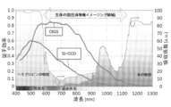
- FIG. 2 is a diagram illustrating the quantum efficiency of the CIGS image sensor 11 and the biological information imaging region.
- the horizontal axis of this figure indicates the wavelength of light.
- the vertical axis (left) of this figure shows the quantum efficiency of the image sensor (CIGS image sensor and Si-CCD image sensor), and the vertical axis (right) shows the absorption coefficient of hemoglobin and water. .
- Si-CCD Si-based CCD [charge-coupled device] element
- Si-CCD has a peak sensitivity in the visible light region and the quantum efficiency in the near infrared region is not so high.
- the CIGS image sensor 11 covers a wide wavelength region from the visible light region to the near infrared region (near 1100 nm) with high quantum efficiency.
- the CIGS image sensor 11 since the CIGS image sensor 11 has high quantum efficiency in a wide wavelength region as compared with the Si-CCD, the photoelectric conversion efficiency for converting light into electricity is high. In addition, since it has high biological permeability, it exhibits high quantum efficiency in a wavelength region around 700 nm to 1100 nm, which is suitable for biological imaging. Therefore, it can be said that the CIGS image sensor 11 is suitable for biological imaging.
- FIG. 3 is a schematic diagram showing a variation factor (deterioration factor of SNR) of input imaging data Din for each pixel.
- the CIGS image sensor 11 has high sensitivity in a wide wavelength region and is suitable for biological imaging.
- the CIGS image sensor 11 has (1) larger dark noise (dark current), (2) sensor sensitivity varies from pixel to pixel, and (3) more defective pixels than the Si-CCD image sensor. ) It has the disadvantage of being easily affected by temperature changes.
- the logic unit 20 causes the input imaging data Din to be subjected to various correction processes (dark noise correction process, sensor sensitivity correction process, defective pixel correction process, etc.). ) To generate output imaging data Dout. Further, the above-mentioned defect (4) is improved by keeping the temperature of the CIGS image sensor 11 constant by using the temperature control unit 40.
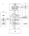
- FIG. 4 is a block diagram illustrating a configuration example of the logic unit 20.
- the logic unit 20 of this configuration example includes a dark noise correction unit 21, a sensor sensitivity correction unit 22, and a defective pixel correction unit 23.
- the correction units 21 to 23 may be implemented in hardware or software.
- the logic unit 20 may include a shutter step correction unit, a digital gain adjustment unit, a LUT [look up table] correction unit (gamma correction unit), and the like in addition to the correction units 21 to 23 described above. .
- the dark noise correction data Ad (x, y) is read from the storage unit 50 (volatile memory 52) to the logic unit 20 and used for correction calculation processing in the dark noise correction unit 21.
- dark noise correction processing here, dark noise for each pixel included in the first pixel data D1 (x, y) can be canceled.
- the sensor sensitivity correction unit 22 multiplies the plurality of second pixel data D2 (x, y) by the sensor sensitivity correction data As (x, y) for each pixel, thereby obtaining a plurality of third pixel data D3 (x, y). y) is generated.
- the sensor sensitivity correction data As (x, y) is read from the storage unit 50 (volatile memory 52) to the logic unit 20 and used for correction calculation processing in the sensor sensitivity correction unit 22.
- the third pixel data D3 (x, y) is output to the defective pixel correction unit 23 at the next stage.
- the defective pixel correction unit 23 converts the defective third pixel data D3 (a, b) out of the plurality of third pixel data D3 (x, y) with its adjacent pixel data (for example, left and right or upper and lower pixel data).
- the fourth pixel data D4 (a, b) is generated by interpolation.
- the third pixel data D3 (c, d) having no defect is directly output as the fourth pixel data D4 (c, d).
- Whether or not the third pixel data D3 (x, y) is defective is determined with reference to a defective pixel flag read from the storage unit 50 (volatile memory 52) to the logic unit 20.
- the fourth pixel data D4 (x, y) is output to the interface unit 30 as the above-described output imaging data Dout.
- the image display delay due to the above series of correction processing is preferably within one frame.
- the dark noise correction data Ad (x, y) and the sensor sensitivity correction data As (x, y) referred to by the logic unit 20 are each a correction table (for example, a correlation table for each pixel and a correction data value).
- csv [comma-separated values] file).
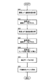
- FIG. 5 is a flowchart showing a dark noise correction table creation operation. This flow is performed before the imaging device 1 is shipped.
- step S10 continuous image acquisition (for example, 60 sheets) of the CIGS image sensor 11 is performed in a dark room.
- the imaging data acquired in this step is exactly the dark noise component itself.
- step S11 a plurality of pieces of imaging data continuously acquired in the dark room are averaged for each pixel, and dark noise correction data Ad (x, y) for each pixel is calculated.
- dark noise correction data Ad (x, y) for each pixel is calculated.
- step S12 a dark noise correction table is created by associating the coordinates P (x, y) for each pixel with the dark noise correction data Ad (x, y).
- step S13 the dark noise correction table is stored in the storage unit 50 (nonvolatile memory 51), and a series of flows is completed.
- FIG. 6 is a register map of dark noise correction data Ad (x, y).
- the lower 12 bits of 16-bit dark noise correction data Ad (x, y) are assigned as an integer part, and the most significant 1 bit is used as a defective pixel flag.
- FIG. 7 is a flowchart showing a sensor sensitivity correction table creation operation. As in the previous FIG. 5, this flow is also performed before the imaging apparatus 1 is shipped.
- step S20 continuous image acquisition (for example, 60 sheets) of the CIGS image sensor 11 is performed under uniform light having the first luminance LI1.
- step S21 the plurality of pieces of imaging data continuously acquired with the first luminance LI1 are averaged for each pixel, and the first output average value ave1 (x, y) for each pixel is calculated.
- step S22 continuous image acquisition (for example, 60 sheets) of the CIGS image sensor 11 is performed under uniform light having a second luminance LI2 different from the first luminance LI1.
- step S23 the plurality of pieces of imaging data continuously acquired with the second luminance LI2 are averaged for each pixel, and a second output average value ave2 (x, y) for each pixel is calculated.
- step S25 a sensor sensitivity correction table is created by associating the coordinates P (x, y) for each pixel with the sensor sensitivity correction data As (x, y).
- step S26 the sensor sensitivity correction table is stored in the storage unit 50 (nonvolatile memory 51), and a series of flows is completed.
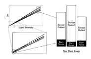
- FIG. 8 is an output characteristic diagram showing a setting example of the first luminance LI1 and the second luminance LI2 at the time of continuous image acquisition. If the brightness is too low, it may be affected by dark noise, and if the brightness is too high, the sensor output may be saturated. Further, if the first luminance LI1 and the second luminance LI2 are too close, there is a possibility that correct sensor sensitivity (tilt) cannot be obtained. In view of these, for example, the first luminance LI1 and the second luminance LI2 are desirably set to luminance levels of 1/3 and 2/3 of the input dynamic range, as shown in the figure.
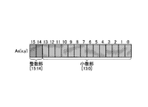
- FIG. 9 is a register map of the sensor sensitivity correction data As (x, y).
- the upper 2 bits are assigned as an integer part
- the lower 14 bits are assigned as a decimal part.
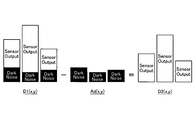
- FIG. 10 is a schematic diagram showing the calculation contents of the dark noise correction unit 21.
- the dark noise correction unit 21 subtracts the dark noise correction data Ad (x, y) for each pixel from the first pixel data D1 (x, y).
- Second pixel data D2 (x, y) is generated. If the second pixel data D2 (x, y) is equal to or lower than 0LSB as a result of the subtraction process in the dark noise correction unit 21, it is only necessary to clip at 0LSB.
- the first pixel data D1 (x, y) can be expressed by the following equation (1).
- the second pixel data D2 (x, y) obtained by subtracting the dark noise correction data Ad (x, y) for each pixel from the first pixel data D1 (x, y) is the following (2). It can be expressed by a formula.
- the dark noise correction data Ad (x, y) corresponding to the dark noise component B (x, y) for each pixel is set, the dark noise component B (x, y) for each pixel is canceled.
- the second pixel data D2 (x, y) thus obtained can be obtained.
- FIG. 11 is a schematic diagram showing the calculation contents of the sensor sensitivity correction unit 22.
- the sensor sensitivity correction unit 22 multiplies the second pixel data D2 (x, y) by the sensor sensitivity correction data As (x, y) to thereby generate the third pixel.
- Data D3 (x, y) is generated.
- the third pixel data D3 (x, y) is 4095LSB or more as a result of the multiplication process in the sensor sensitivity correction unit 22, it may be clipped at 4095LSB.
- the third pixel data D3 (x, y) obtained by multiplying the second pixel data D2 (x, y) by the sensor sensitivity correction data As (x, y) for each pixel is expressed by the following (3). It can be expressed by a formula.
- the sensor sensitivity correction data As (x, y) corresponding to the reciprocal of the sensor sensitivity A (x, y) for each pixel is set, the sensor sensitivity A (x, y) for each pixel is uniform.
- the third pixel data D3 (x, y) arranged in the above can be obtained.
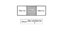
- FIG. 12 is a schematic diagram showing the calculation contents of the defective pixel correction unit 23.
- the defective pixel correction unit 23 converts the defective third pixel data D3 (a, b) out of the plurality of third pixel data D3 (x, y).
- the fourth pixel data D4 (a, b) is generated by interpolating with adjacent pixel data (for example, left and right or upper and lower pixel data).
- the fourth pixel data D4 (a, b) for interpolation is calculated by calculating the average value of (a + 1, b).
- the defective pixels of the CIGS image sensor 11 can be made inconspicuous.
- Defect pixel determination may be performed when the dark noise correction table described above with reference to FIG. 5 is created. More specifically, when the dark noise correction data Ad (x, y) for each pixel is calculated, pixels whose calculated values are higher than the upper limit value and lower than the lower limit value are defective pixels. And “1” may be set in the defective pixel flag.
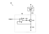
- FIG. 13 is a circuit diagram illustrating a configuration example of the temperature control unit 40.
- the drive circuit 42 includes an npn bipolar transistor 421, an operational amplifier 422, and resistors 423 and 424.
- the collector of the transistor 421 is connected to the Peltier element 41 as the output terminal of the drive current Idrv.
- the base of the transistor 421 is connected to the first end of the resistor 423.
- a second terminal of the resistor 423 is connected to the output terminal of the operational amplifier 422.
- the emitter of the transistor 421 is connected to the inverting input terminal ( ⁇ ) of the operational amplifier 422 and the first terminal of the resistor 424.
- a second end of the resistor 424 is connected to a reference potential end (ground end).
- the non-inverting input terminal (+) of the operational amplifier 422 is connected to the input terminal of the PWM signal.
- the operational amplifier 422 feedback-controls the base voltage of the transistor 421 so that an imaginary short circuit occurs between the non-inverting input terminal (+) and the inverting input terminal ( ⁇ ).
- the drive current Idrv (for example, 200 mA) is turned on / off in the Peltier element 41 according to the duty of the PWM signal.
- the PWM signal is generated in the logic unit 20. More specifically, the logic unit 20 sequentially calculates the average output value AVE of the light-shielded pixels (OPB pixels) included in the CIGS image sensor 11 for each frame, and the average output value AVE one frame before is greater than or equal to the threshold value. The logic level (high / low) of the PWM signal is switched according to whether or not there is.
- the period during which the drive current Idrv flows through the Peltier element 41 is extended, so that the temperature of the CIGS image sensor 11 is further lowered.
- the invention disclosed in the present specification can be used, for example, in an optical imaging medical system for non-invasively observing a living body.
Landscapes
- Engineering & Computer Science (AREA)
- Multimedia (AREA)
- Signal Processing (AREA)
- Transforming Light Signals Into Electric Signals (AREA)
Abstract
画像補正装置20は、イメージセンサ11を形成している複数の受光素子P(x,y)で得られる複数の第1画素データD1(x,y)から画素毎のダークノイズ補正データAd(x,y)を減算することにより複数の第2画素データD2(x,y)を生成するダークノイズ補正部21と、複数の第2画素データD2(x,y)に画素毎のセンサ感度補正データAs(x,y)を乗算することにより複数の第3画素データD3(x,y)を生成するセンサ感度補正部22と、を有する。
Description
本発明は、画像補正装置、撮像装置、及び、補正テーブル作成方法に関する。
本願出願人による特許文献1では、均一な光電変換領域にAlグリッドパターンを形成することにより、SNR[signal-to-noise ratio]を改善する技術が提案されている。
しかしながら、特許文献1の従来技術では、Alグリッドパターンにより光電変換領域の開口率が低下するという課題があった。
本明細書中に開示されている発明は、本願の発明者らにより見出された上記の課題に鑑み、光電変換領域の開口率を下げずにSNRを改善することのできる画像補正装置、撮像装置、及び、補正テーブル作成方法を提供することを目的とする。
本明細書中に開示されている画像補正装置は、イメージセンサを形成する複数の受光素子で得られる複数の第1画素データから画素毎のダークノイズ補正データを減算することにより複数の第2画素データを生成するダークノイズ補正部と、前記複数の第2画素データに画素毎のセンサ感度補正データを乗算することにより複数の第3画素データを生成するセンサ感度補正部と、を有する構成(第1の構成)とされている。
なお、上記第1の構成から成る画像補正装置は、欠陥のある第3画素データを隣接画素データで補間することにより第4画素データを生成する欠陥画素補正部をさらに有する構成(第2の構成)にするとよい。
また、本明細書中に開示されている撮像装置は、イメージセンサを用いて入力撮像データを生成する撮像部と、前記入力撮像データを補正して出力撮像データを生成する上記第1または第2の構成から成る画像補正装置とを有する構成(第3の構成)とされている。
なお、上記第3の構成から成る撮像装置において、前記イメージセンサは、CIGSイメージセンサである構成(第4の構成)にするとよい。
また、上記第3または第4の構成から成る撮像装置は、前記ダークノイズ補正データ及び前記センサ感度補正データを格納する記憶部をさらに有する構成(第5の構成)にするとよい。
また、上記第5の構成から成る撮像装置において、前記記憶部は、前記ダークノイズ補正データ及び前記センサ感度補正データを不揮発的に格納する不揮発性メモリと、前記不揮発性メモリよりもアクセス速度の速い揮発性メモリと、を含み、前記画像補正装置は、前記撮像装置の起動時に前記不揮発性メモリから前記揮発性メモリにロードされるダークノイズ補正データ及びセンサ感度補正データを用いて前記入力撮像データを補正する構成(第6の構成)にするとよい。
また、上記第3~第6いずれかの構成から成る撮像装置は、前記イメージセンサの温度を目標値に調整する温度制御部をさらに有する構成(第7の構成)にするとよい。
また、上記第7の構成から成る撮像装置において、前記温度制御部は、前記イメージセンサに取り付けられるペルチェ素子と、前記イメージセンサに含まれる遮光画素の出力値と所定の閾値との比較結果に応じて前記ペルチェ素子を駆動する駆動回路と、を含む構成(第8の構成)にするとよい。
また、本明細書中に開示されている補正テーブル作成方法は、暗室でイメージセンサの連続画像取得を行うステップと、前記暗室で連続取得された複数枚分の撮像データを画素毎に平均化して画素毎のダークノイズ補正データを算出するステップと、画素の座標とダークノイズ補正データとを関連付けることによりダークノイズ補正テーブルを作成するステップとを有する構成(第9の構成)とされている。
また、本明細書中に開示されている補正テーブル作成方法は、第1輝度でイメージセンサの連続画像取得を行うステップと、前記第1輝度で連続取得された複数枚分の撮像データを画素毎に平均化して画素毎の第1出力平均値を算出するステップと、前記第1輝度とは異なる第2輝度でイメージセンサの連続画像取得を行うステップと、前記第2輝度で連続取得された複数枚分の撮像データを画素毎に平均化して画素毎の第2出力平均値を算出するステップと、画素毎の前記第1出力平均値と前記第2出力平均値から画素毎のセンサ感度補正データを算出するステップと、画素の座標とセンサ感度補正データとを関連付けることによりセンサ感度補正テーブルを作成するステップと、を有する構成(第10の構成)とされている。
本明細書中に開示されている発明によれば、光電変換領域の開口率を下げずにSNRを改善することのできる画像補正装置、撮像装置、及び、補正テーブル作成方法を提供することが可能となる。
<撮像システム>
図1は、撮像システムXの一構成例を示すブロック図である。本構成例の撮像システムXは、撮像装置1とパソコン2を有する。なお、詳細については後述するが、本構成例の撮像システムXは、例えば、CIGSイメージセンサ11を活用して生体を非侵襲的に観察する光学的イメージング医療システムとして利用することができる。
図1は、撮像システムXの一構成例を示すブロック図である。本構成例の撮像システムXは、撮像装置1とパソコン2を有する。なお、詳細については後述するが、本構成例の撮像システムXは、例えば、CIGSイメージセンサ11を活用して生体を非侵襲的に観察する光学的イメージング医療システムとして利用することができる。
撮像装置1は、被写体像を撮影してデジタル撮像データを生成するカメラモジュールである。例えば、撮像システムXを光学的イメージング医療システムとして利用する場合、撮像装置1では、生体に光源光(可視光や近赤外光など)を照射して生体から戻ってくる反射光を受光することにより生体像の撮影が行われる。
撮像装置1とパソコン2との間は、USB[universal serial bus]ケーブルを用いて有線接続されており、当該USBケーブルを介して相互間の信号伝達やパソコン2から撮像装置1への電力供給が行われる。ただし、撮像装置1への電力供給については、別途のACアダプタを用いて行うことも可能である。また、撮像装置1にリチウムイオン二次電池などを搭載すれば、撮像装置1をバッテリ駆動とすることも可能である。
パソコン2は、撮像システムXを統括的に制御する主体であり、撮像装置1の動作制御や各種設定を行ったり、撮像装置1で得られたデジタル撮像データに基づいて被写体像の作成、表示、解析、ないしは、記録を行ったりする。なお、パソコン2としては、汎用的なノートPCやデスクトップPCを採用してもよいし、撮像システムXに最適化された専用端末を採用してもよい。或いは、広く一般に普及している携帯情報端末(タブレット端末やスマートフォンなど)を用いても構わない。
<撮像装置>
引き続き、図1を参照しながら撮像装置1の構成及び動作について説明する。本構成例の撮像装置1は、撮像部10と、ロジック部20と、インタフェイス部30と、温度制御部40と、記憶部50と、発振部60と、電源部70と、を含む。
引き続き、図1を参照しながら撮像装置1の構成及び動作について説明する。本構成例の撮像装置1は、撮像部10と、ロジック部20と、インタフェイス部30と、温度制御部40と、記憶部50と、発振部60と、電源部70と、を含む。
撮像部10は、CIGSイメージセンサ11を用いて被写体像を撮影することにより、入力撮像データDinを生成してロジック部20に出力する。例えば、撮像システムXを光学的イメージング医療システムとして利用する場合、撮像部10には、CIGSイメージセンサ11のほか、生体に可視光や近赤外光を照射するためのLED[light emitting diode]光源や、生体から戻ってくる反射光をCIGSイメージセンサ11に結像させるための光学部材(C/CSマウントレンズなど)を含めるとよい。
なお、CIGSイメージセンサ11は、入射光を電気信号に変換する電子デバイス(光電変換デバイス)の一種である。CIGSは、銅(Cu)、インジウム(In)、ガリウム(Ga)、及び、セレン(Se)から成る化合物半導体であり、一般的なシリコン(Si)よりも幅広い波長の光を電気に光電変換することが可能である(詳細は後述)。
ロジック部20は、入力撮像データDinをリアルタイムに補正して出力撮像データDoutを生成する画像補正装置として機能する。また、ロジック部20は、種々の制御コマンドを用いて撮像部10の動作制御を行う機能も備えている。なお、ロジック部20としては、FPGA[field-programmable gate array]などを用いることが望ましい。
インタフェイス部30は、撮像装置1(ロジック部20)とパソコン2との相互間で出力撮像データDoutや制御コマンドを受け渡すためのフロントエンドである。なお、インタフェイス部30としては、例えば、USB[universal serial bus]規格に準拠した汎用のシリアルインタフェイスを採用することが望ましい。
温度制御部40は、CIGSイメージセンサ11の温度を目標値に調整するための手段であり、ペルチェ素子41と駆動回路42を含む。
ペルチェ素子41は、CIGSイメージセンサ11に取り付けられた板状の半導体素子であり、ペルチェ効果を利用してCIGSイメージセンサ11を冷却する。なお、ペルチェ素子41を複数重ねることにより、熱の移動量を増やすことが可能である。
駆動回路42は、ロジック部20からの制御信号に応じてペルチェ素子41を駆動する電流ドライバである。なお、CIGSイメージセンサ11に含まれる遮光画素(いわゆるOPB[optical black]画素)の出力値は、CIGSイメージセンサ11の温度に依存して指数関数的に変動することが知られている。そこで、駆動回路42は、遮光画素の出力値と所定の閾値との比較結果に応じた制御信号(PWM[pulse width modulation]信号など)を受け取り、ペルチェ素子41の駆動電流量を調整する構成とされている。
このような温度制御部40を設けることにより、熱の影響を比較的受けやすいCIGSイメージセンサ11を一定の温度(例えば25℃)に保つことができるので、SNRを改善することが可能となる。なお、温度制御部40には、ペルチェ素子41や駆動回路42のほかに、ペルチェ素子114の発熱面から放熱を行うためのヒートシンクや、CIGSイメージセンサ11を空冷するための冷却ファンなどを含めてもよい。
記憶部50は、ロジック部20で用いられる種々の補正データ(後述のダークノイズ補正データAd(x,y)やセンサ感度補正データAs(x,y)など)を格納する手段であり、不揮発性メモリ51と揮発性メモリ52を含む。
不揮発性メモリ51は、ロジック部20で用いられる種々の補正データを不揮発的に格納するための半導体メモリである。不揮発性メモリ51としては、フラッシュメモリ、EEPROM[electrically erasable programmable read-only memory]、または、OTPROM[one-time PROM]などを用いることが望ましい。
揮発性メモリ52は、主にロジック部20の作業領域として用いられる半導体メモリである。揮発性メモリ52としては、不揮発性メモリ51よりもアクセス速度の速いSDRAM[synchronous dynamic random access memory]などを用いることが望ましい。
ロジック部20は、撮像装置1の起動時(電源投入時)に不揮発性メモリ51から揮発性メモリ52にロードされる種々の補正データを用いて入力撮像データDinをリアルタイムに補正することにより出力撮像データDoutを生成する。なお、ロジック部20が十分なレジスタ容量を持っている場合には、揮発性メモリ52を省略してもよい。
発振部60は、ロジック部20の駆動に必要なクロック信号(例えば162MHz)を生成する手段(水晶発振器など)である。
電源部70は、撮像装置1の各部に電力供給を行うための手段(DC/DCコンバータなど)である。
<CIGSイメージセンサ>
図2は、CIGSイメージセンサ11の量子効率と生体情報イメージング領域を示す図である。本図の横軸は光の波長を示している。また、本図の縦軸(左)は撮像素子(CIGSイメージセンサ、及び、Si-CCDイメージセンサ)の量子効率を示しており、縦軸(右)はヘモグロビンと水の吸収係数を示している。なお、撮像素子(受光素子)の量子効率ηは、入射光子量に対して発生するキャリア数(出力電流)の比(η=(hc/qλ)×(I/p)、ただし、h:プランク定数、c:真空中の光速度、q:電子電荷、λ:波長、I:出力電流、p:入射光子量)として定義される。
図2は、CIGSイメージセンサ11の量子効率と生体情報イメージング領域を示す図である。本図の横軸は光の波長を示している。また、本図の縦軸(左)は撮像素子(CIGSイメージセンサ、及び、Si-CCDイメージセンサ)の量子効率を示しており、縦軸(右)はヘモグロビンと水の吸収係数を示している。なお、撮像素子(受光素子)の量子効率ηは、入射光子量に対して発生するキャリア数(出力電流)の比(η=(hc/qλ)×(I/p)、ただし、h:プランク定数、c:真空中の光速度、q:電子電荷、λ:波長、I:出力電流、p:入射光子量)として定義される。
一般的な固体撮像素子としては、Si-CCD(SiベースのCCD[charge coupled device]素子)が広く利用されている。しかし、Si-CCDは、可視光領域にピーク感度を持ち、近赤外領域の量子効率はさほど高くない。一方、CIGSイメージセンサ11は、可視光領域から近赤外領域(1100nm付近)までの幅広い波長領域を高い量子効率でカバーしている。
このように、CIGSイメージセンサ11は、Si-CCDと比較して幅広い波長領域において量子効率が高いので、光を電気に変換する光電変換効率が高い。また、生体透過性が高いので、生体イメージングに適するとされる700nm~1100nm前後の波長領域で高い量子効率を示す。従って、CIGSイメージセンサ11は、生体イメージングに適していると言える。
<ばらつき要因>
図3は、画素毎における入力撮像データDinのばらつき要因(SNRの悪化要因)を示す模式図である。先に述べたように、CIGSイメージセンサ11は、幅広い波長領域で高い感度を持っており、生体イメージングに適している。ただし、CIGSイメージセンサ11は、Si-CCDイメージセンサと比べて、(1)ダークノイズ(暗電流)が大きい、(2)画素毎のセンサ感度がばらつく、(3)欠陥画素が多い、(4)温度変化の影響を受けやすい、といった欠点を持つ。
図3は、画素毎における入力撮像データDinのばらつき要因(SNRの悪化要因)を示す模式図である。先に述べたように、CIGSイメージセンサ11は、幅広い波長領域で高い感度を持っており、生体イメージングに適している。ただし、CIGSイメージセンサ11は、Si-CCDイメージセンサと比べて、(1)ダークノイズ(暗電流)が大きい、(2)画素毎のセンサ感度がばらつく、(3)欠陥画素が多い、(4)温度変化の影響を受けやすい、といった欠点を持つ。
そこで、上記の欠点(1)~(3)を解消すべく、ロジック部20には、入力撮像データDinに種々の補正処理(ダークノイズ補正処理、センサ感度補正処理、及び、欠陥画素補正処理など)を施して出力撮像データDoutを生成する画像補正機能が具備されている。また、上記の欠点(4)については、温度制御部40を用いてCIGSイメージセンサ11の温度を一定に保つことにより改善が図られている。
<ロジック部>
図4は、ロジック部20の一構成例を示すブロック図である。本構成例のロジック部20は、ダークノイズ補正部21と、センサ感度補正部22と、欠陥画素補正部23とを含む。なお、各補正部21~23については、ハードウェア的に実装してもよいし、ソフトウェア的に実装してもよい。また、ロジック部20には、上記した各補正部21~23のほか、シャッター段差補正部、デジタルゲイン調整部、及び、LUT[look up table]補正部(ガンマ補正部)などを含めてもよい。
図4は、ロジック部20の一構成例を示すブロック図である。本構成例のロジック部20は、ダークノイズ補正部21と、センサ感度補正部22と、欠陥画素補正部23とを含む。なお、各補正部21~23については、ハードウェア的に実装してもよいし、ソフトウェア的に実装してもよい。また、ロジック部20には、上記した各補正部21~23のほか、シャッター段差補正部、デジタルゲイン調整部、及び、LUT[look up table]補正部(ガンマ補正部)などを含めてもよい。
ダークノイズ補正部21は、CIGSイメージセンサ11を形成する複数の受光素子P(x,y)で各々得られる複数の第1画素データD1(x,y)(=先述の入力撮像データDinに相当、例えば12ビット)から、画素毎のダークノイズ補正データAd(x,y)を各々減算することにより、複数の第2画素データD2(x,y)を生成する。ダークノイズ補正データAd(x,y)は、記憶部50(揮発性メモリ52)からロジック部20に読み出されてダークノイズ補正部21での補正演算処理に供される。ここでのダークノイズ補正処理により、第1画素データD1(x,y)に含まれる画素毎のダークノイズをキャンセルすることができる。なお、第2画素データD2(x,y)は、次段のセンサ感度補正部22に出力される一方、CIGSイメージセンサ11の温度制御に必要となるPWM信号生成処理(=遮光画素の出力値と所定の閾値との比較処理)にも供される。
センサ感度補正部22は、複数の第2画素データD2(x,y)に画素毎のセンサ感度補正データAs(x,y)を各々乗算することにより、複数の第3画素データD3(x,y)を生成する。センサ感度補正データAs(x,y)は、記憶部50(揮発性メモリ52)からロジック部20に読み出されてセンサ感度補正部22での補正演算処理に供される。ここでのセンサ感度補正処理により、画素毎のセンサ感度(=光強度に対するセンサ出力値の傾き)を均一に揃えることができる。なお、第3画素データD3(x,y)は、次段の欠陥画素補正部23に出力される。
欠陥画素補正部23は、複数の第3画素データD3(x,y)のうち、欠陥のある第3画素データD3(a,b)をその隣接画素データ(例えば左右または上下の画素データ)で補間することにより、第4画素データD4(a,b)を生成する。一方、欠陥のない第3画素データD3(c,d)については、そのまま第4画素データD4(c,d)としてスルー出力される。第3画素データD3(x,y)に欠陥があるか否かについては、記憶部50(揮発性メモリ52)からロジック部20に読み出される欠陥画素フラグを参照して判断される。ここでの欠陥画素補正処理により、CIGSイメージセンサ11の欠陥画素を目立たなくすることができる。なお、第4画素データD4(x、y)は、先述の出力撮像データDoutとしてインターフェイス部30に出力される。
上記一連の補正処理による画像表示遅延は、1フレーム以内であることが望ましい。このような高速演算システムによるリアルタイム補正を実現することにより、動画/静止画の両方に対応することが可能となる。
なお、ロジック部20で参照されるダークノイズ補正データAd(x,y)とセンサ感度補正データAs(x,y)は、それぞれ、画素毎の座標と補正データ値とを関連付けた補正テーブル(例えばcsv[comma-separated values]ファイル)として、記憶部50に格納されている。以下、補正テーブルの作成方法について詳述する。
<ダークノイズ補正テーブル作成>
図5は、ダークノイズ補正テーブルの作成動作を示すフローチャートである。本フローは、撮像装置1の出荷前に実施される。本フローが開始されると、まず、ステップS10では、暗室でCIGSイメージセンサ11の連続画像取得(例えば60枚)が行われる。本ステップで取得される撮像データは、正にダークノイズ成分そのものである。
図5は、ダークノイズ補正テーブルの作成動作を示すフローチャートである。本フローは、撮像装置1の出荷前に実施される。本フローが開始されると、まず、ステップS10では、暗室でCIGSイメージセンサ11の連続画像取得(例えば60枚)が行われる。本ステップで取得される撮像データは、正にダークノイズ成分そのものである。
次に、ステップS11では、暗室で連続取得された複数枚分の撮像データが画素毎に平均化されて画素毎のダークノイズ補正データAd(x,y)が算出される。このように、画素毎のダークノイズ成分を平均化することにより、より正しいダークノイズ補正データAd(x,y)を取得することが可能となる。
次に、ステップS12では、画素毎の座標P(x,y)と、ダークノイズ補正データAd(x,y)とを関連付けることにより、ダークノイズ補正テーブルが作成される。
最後に、ステップS13では、ダークノイズ補正テーブルが記憶部50(不揮発性メモリ51)に格納されて、一連のフローが終了される。
図6は、ダークノイズ補正データAd(x,y)のレジスタマップである。本図の例では、16ビットのダークノイズ補正データAd(x,y)のうち、下位12ビットが整数部として割り当てられており、最上位1ビットが欠陥画素フラグとして流用されている。
<センサ感度補正テーブル作成>
図7は、センサ感度補正テーブルの作成動作を示すフローチャートである。先の図5と同様、本フローも、撮像装置1の出荷前に実施される。本フローが開始されると、まず、ステップS20では、第1輝度LI1を持つ均一な光の下でCIGSイメージセンサ11の連続画像取得(例えば60枚)が行われる。
図7は、センサ感度補正テーブルの作成動作を示すフローチャートである。先の図5と同様、本フローも、撮像装置1の出荷前に実施される。本フローが開始されると、まず、ステップS20では、第1輝度LI1を持つ均一な光の下でCIGSイメージセンサ11の連続画像取得(例えば60枚)が行われる。
次に、ステップS21では、第1輝度LI1で連続取得された複数枚分の撮像データが画素毎に平均化されて画素毎の第1出力平均値ave1(x,y)が算出される。
次に、ステップS22では、第1輝度LI1とは異なる第2輝度LI2を持つ均一な光の下でCIGSイメージセンサ11の連続画像取得(例えば60枚)が行われる。
次に、ステップS23では、第2輝度LI2で連続取得された複数枚分の撮像データが画素毎に平均化されて画素毎の第2出力平均値ave2(x,y)が算出される。
次に、ステップS24では、画素毎の第1出力平均値ave1(x,y)と第2出力平均値ave2(x,y)との差分から画素毎のセンサ感度A’(x,y)(={ave2(x,y)-ave1(x,y)}/(LI2-LI1))が算出され、さらに、その算出結果から画素毎のセンサ感度補正データAs(x,y)(=EV/A’(x,y)、ただし、EVは所定の期待値)が算出される。
次に、ステップS25では、画素毎の座標P(x,y)と、センサ感度補正データAs(x,y)とを関連付けることにより、センサ感度補正テーブルが作成される。
最後に、ステップS26では、センサ感度補正テーブルが記憶部50(不揮発性メモリ51)に格納されて、一連のフローが終了される。
図8は、連続画像取得時における第1輝度LI1と第2輝度LI2の設定例を示す出力特性図である。輝度が低過ぎる領域ではダークノイズの影響を受けるおそれがあり、輝度が高過ぎる領域ではセンサ出力が飽和してしまうおそれがある。また、第1輝度LI1と第2輝度LI2が近過ぎると、正しいセンサ感度(傾き)を得られないおそれがある。これらを鑑みると、例えば、第1輝度LI1と第2輝度LI2は、本図で示すように、入力ダイナミックレンジの1/3と2/3の輝度レベルに設定することが望ましい。
図9は、センサ感度補正データAs(x,y)のレジスタマップである。本図の例では16ビットのセンサ感度補正データAs(x,y)のうち、上位2ビットが整数部として割り当てられており、下位14ビットが小数部として割り当てられている。
<ダークノイズ補正部>
図10は、ダークノイズ補正部21の演算内容を示す模式図である。先出の図4でも概略的に説明したが、ダークノイズ補正部21は、第1画素データD1(x,y)から、画素毎のダークノイズ補正データAd(x,y)を減算することにより、第2画素データD2(x,y)を生成する。なお、ダークノイズ補正部21での減算処理により、第2画素データD2(x,y)が0LSB以下となる場合には、0LSBでクリップすればよい。
図10は、ダークノイズ補正部21の演算内容を示す模式図である。先出の図4でも概略的に説明したが、ダークノイズ補正部21は、第1画素データD1(x,y)から、画素毎のダークノイズ補正データAd(x,y)を減算することにより、第2画素データD2(x,y)を生成する。なお、ダークノイズ補正部21での減算処理により、第2画素データD2(x,y)が0LSB以下となる場合には、0LSBでクリップすればよい。
ところで、画素毎のセンサ感度をA(x,y)、画素毎のダークノイズ成分をB(x,y)、CIGSイメージセンサ11に入射される光の輝度をLIとした場合、第1画素データD1(x,y)は、次の(1)式で表すことができる。
D1(x,y)=A(x,y)×LI+B(x,y) … (1)
一方、第1画素データD1(x,y)から画素毎のダークノイズ補正データAd(x,y)を減算することにより得られる第2画素データD2(x,y)は、次の(2)式で表すことができる。
D2(x,y)=D1(x,y)-Ad(x,y)
=A(x,y)×LI+B(x,y)-Ad(x,y)
≒A(x,y)×LI … (2)
=A(x,y)×LI+B(x,y)-Ad(x,y)
≒A(x,y)×LI … (2)
このように、画素毎のダークノイズ成分B(x,y)に相当するダークノイズ補正データAd(x,y)を設定しておけば、画素毎のダークノイズ成分B(x,y)がキャンセルされた第2画素データD2(x,y)を得ることができる。
<センサ感度補正部>
図11は、センサ感度補正部22の演算内容を示す模式図である。先出の図4でも概略的に説明したが、センサ感度補正部22は、第2画素データD2(x,y)にセンサ感度補正データAs(x,y)を乗算することにより、第3画素データD3(x,y)を生成する。なお、センサ感度補正部22での乗算処理により、第3画素データD3(x,y)が4095LSB以上となる場合には、4095LSBでクリップすればよい。
図11は、センサ感度補正部22の演算内容を示す模式図である。先出の図4でも概略的に説明したが、センサ感度補正部22は、第2画素データD2(x,y)にセンサ感度補正データAs(x,y)を乗算することにより、第3画素データD3(x,y)を生成する。なお、センサ感度補正部22での乗算処理により、第3画素データD3(x,y)が4095LSB以上となる場合には、4095LSBでクリップすればよい。
ところで、第2画素データD2(x,y)に画素毎のセンサ感度補正データAs(x,y)を乗算することにより得られる第3画素データD3(x,y)は、次の(3)式で表すことができる。
D3(x,y)=D2(x,y)×As(x,y)
=A(x,y)×LI×EV/A’(x,y)
≒EV×LI … (3)
=A(x,y)×LI×EV/A’(x,y)
≒EV×LI … (3)
このように、画素毎のセンサ感度A(x,y)の逆数に相当するセンサ感度補正データAs(x,y)を設定しておけば、画素毎のセンサ感度A(x,y)を均一に揃えた第3画素データD3(x,y)を得ることができる。
<欠陥画素補正部>
図12は、欠陥画素補正部23の演算内容を示す模式図である。先出の図4でも概略的に説明したが、欠陥画素補正部23は、複数の第3画素データD3(x,y)のうち、欠陥のある第3画素データD3(a,b)をその隣接画素データ(例えば左右または上下の画素データ)で補間することにより、第4画素データD4(a,b)を生成する。
図12は、欠陥画素補正部23の演算内容を示す模式図である。先出の図4でも概略的に説明したが、欠陥画素補正部23は、複数の第3画素データD3(x,y)のうち、欠陥のある第3画素データD3(a,b)をその隣接画素データ(例えば左右または上下の画素データ)で補間することにより、第4画素データD4(a,b)を生成する。
本図の例では、次の(4)式で表されるように、欠陥のある第3画素データD3(a,b)の左右に位置する隣接画素データD3(a-1,b)及びD3(a+1,b)の平均値を求めることにより、補間用の第4画素データD4(a,b)が算出されている。
D4(a,b)={D3(a-1,b)+D3(a+1,b)}/2 … (4)
このような欠陥画素補正によれば、CIGSイメージセンサ11の欠陥画素を目立たなくすることができる。なお、欠陥画素の判定(欠陥画素フラグの設定)は、先出の図5で説明したダークノイズ補正テーブル作成時に行っておけばよい。具体的に述べると、画素毎のダークノイズ補正データAd(x,y)を算出した際、その算出値が上限値よりも高い画素と下限値よりも低い画素については、これを欠陥画素であると判定し、欠陥画素フラグに「1」を立てておけばよい。
<温度制御部>
図13は、温度制御部40の一構成例を示す回路図である。本構成例の温度制御部40において、駆動回路42は、npn型バイポーラトランジスタ421と、オペアンプ422と、抵抗423及び424と、を含む。
図13は、温度制御部40の一構成例を示す回路図である。本構成例の温度制御部40において、駆動回路42は、npn型バイポーラトランジスタ421と、オペアンプ422と、抵抗423及び424と、を含む。
トランジスタ421のコレクタは、駆動電流Idrvの出力端としてペルチェ素子41に接続されている。トランジスタ421のベースは、抵抗423の第1端に接続されている。抵抗423の第2端は、オペアンプ422の出力端に接続されている。トランジスタ421のエミッタは、オペアンプ422の反転入力端(-)と抵抗424の第1端に各々接続されている。抵抗424の第2端は、基準電位端(接地端)に接続されている。オペアンプ422の非反転入力端(+)は、PWM信号の入力端に接続されている。
上記構成から成る駆動回路42において、オペアンプ422は、非反転入力端(+)と反転入力端(-)との間がイマジナリーショートするように、トランジスタ421のベース電圧を帰還制御する。その結果、ペルチェ素子41には、PWM信号のデューティに応じて駆動電流Idrv(例えば200mA)がオン/オフされる。
なお、上記のPWM信号は、ロジック部20において生成される。より具体的に述べると、ロジック部20は、CIGSイメージセンサ11に含まれる遮光画素(OPB画素)の出力平均値AVEをフレーム毎に順次算出し、1フレーム前の出力平均値AVEが閾値以上であるか否かに応じてPWM信号の論理レベル(ハイ/ロー)を切り替える。
例えば、CIGSイメージセンサ11の温度が高いほど、遮光画素の出力平均値AVEが上昇してPWM信号のハイレベル期間が長くなる。その結果、ペルチェ素子41に駆動電流Idrvを流す期間が延びるので、CIGSイメージセンサ11の温度がより引き下げられる。このような駆動電流IdrvのPWM制御により、CIGSイメージセンサ11の温度を目標値に維持することが可能となる。
<補正効果>
図14は、補正前後の出力比較図である。なお、(a)欄には補正前のキャプチャー画像が示されており、(b)欄には補正後のキャプチャー画像が示されている。出力画像の品質(SNR=20×log(Ave/σ)、ただしAveは出力平均、σは標準偏差)は、ロジック部20での各種補正により、大幅に改善されていることが分かる(SNR=21dB→34dB)。
図14は、補正前後の出力比較図である。なお、(a)欄には補正前のキャプチャー画像が示されており、(b)欄には補正後のキャプチャー画像が示されている。出力画像の品質(SNR=20×log(Ave/σ)、ただしAveは出力平均、σは標準偏差)は、ロジック部20での各種補正により、大幅に改善されていることが分かる(SNR=21dB→34dB)。
<その他の変形例>
なお、本明細書中に開示されている種々の技術的特徴は、上記実施形態のほか、その技術的創作の主旨を逸脱しない範囲で種々の変更を加えることが可能である。すなわち、上記実施形態は、全ての点で例示であって制限的なものではないと考えられるべきであり、本発明の技術的範囲は、上記実施形態の説明ではなく、特許請求の範囲によって示されるものであり、特許請求の範囲と均等の意味及び範囲内に属する全ての変更が含まれると理解されるべきである。
なお、本明細書中に開示されている種々の技術的特徴は、上記実施形態のほか、その技術的創作の主旨を逸脱しない範囲で種々の変更を加えることが可能である。すなわち、上記実施形態は、全ての点で例示であって制限的なものではないと考えられるべきであり、本発明の技術的範囲は、上記実施形態の説明ではなく、特許請求の範囲によって示されるものであり、特許請求の範囲と均等の意味及び範囲内に属する全ての変更が含まれると理解されるべきである。
本明細書中に開示されている発明は、例えば、生体を非侵襲的に観察するための光学的イメージング医療システムに利用することが可能である。
X 撮像システム
1 撮像装置
2 パソコン
10 撮像部
11 CIGSイメージセンサ
20 ロジック部(画像補正装置)
21 ダークノイズ補正部
22 センサ感度補正部
23 欠陥画素補正部
30 インタフェイス部
40 温度制御部
41 ペルチェ素子
42 駆動回路
421 npn型バイポーラトランジスタ
422 オペアンプ
423、424 抵抗
50 記憶部
51 不揮発性メモリ
52 揮発性メモリ
60 発振部
70 電源部
1 撮像装置
2 パソコン
10 撮像部
11 CIGSイメージセンサ
20 ロジック部(画像補正装置)
21 ダークノイズ補正部
22 センサ感度補正部
23 欠陥画素補正部
30 インタフェイス部
40 温度制御部
41 ペルチェ素子
42 駆動回路
421 npn型バイポーラトランジスタ
422 オペアンプ
423、424 抵抗
50 記憶部
51 不揮発性メモリ
52 揮発性メモリ
60 発振部
70 電源部
Claims (10)
- イメージセンサを形成する複数の受光素子で得られる複数の第1画素データから画素毎のダークノイズ補正データを減算することにより複数の第2画素データを生成するダークノイズ補正部と、
前記複数の第2画素データに画素毎のセンサ感度補正データを乗算することにより複数の第3画素データを生成するセンサ感度補正部と、
を有することを特徴とする画像補正装置。 - 欠陥のある第3画素データを隣接画素データで補間することにより第4画素データを生成する欠陥画素補正部をさらに有することを特徴とする請求項1に記載の画像補正装置。
- イメージセンサを用いて入力撮像データを生成する撮像部と、
前記入力撮像データを補正して出力撮像データを生成する請求項1または請求項2に記載の画像補正装置と、
を有することを特徴とする撮像装置。 - 前記イメージセンサは、CIGSイメージセンサであることを特徴とする請求項3に記載の撮像装置。
- 前記ダークノイズ補正データ及び前記センサ感度補正データを格納する記憶部をさらに有することを特徴とする請求項3または請求項4に記載の撮像装置。
- 前記記憶部は、前記ダークノイズ補正データ及び前記センサ感度補正データを不揮発的に格納する不揮発性メモリと、前記不揮発性メモリよりもアクセス速度の速い揮発性メモリと、を含み、
前記画像補正装置は、前記撮像装置の起動時に前記不揮発性メモリから前記揮発性メモリにロードされるダークノイズ補正データ及びセンサ感度補正データを用いて前記入力撮像データを補正することを特徴とする請求項5に記載の撮像装置。 - 前記イメージセンサの温度を目標値に調整する温度制御部をさらに有することを特徴とする請求項3~請求項6のいずれか一項に記載の撮像装置。
- 前記温度制御部は、前記イメージセンサに取り付けられるペルチェ素子と、前記イメージセンサに含まれる遮光画素の出力値と所定の閾値との比較結果に応じて前記ペルチェ素子を駆動する駆動回路と、を含むことを特徴とする請求項7に記載の撮像装置。
- 暗室でイメージセンサの連続画像取得を行うステップと、
前記暗室で連続取得された複数枚分の撮像データを画素毎に平均化して画素毎のダークノイズ補正データを算出するステップと、
画素の座標とダークノイズ補正データとを関連付けることによりダークノイズ補正テーブルを作成するステップと、
を有することを特徴とする補正テーブル作成方法。 - 第1輝度でイメージセンサの連続画像取得を行うステップと、
前記第1輝度で連続取得された複数枚分の撮像データを画素毎に平均化して画素毎の第1出力平均値を算出するステップと、
前記第1輝度とは異なる第2輝度でイメージセンサの連続画像取得を行うステップと、
前記第2輝度で連続取得された複数枚分の撮像データを画素毎に平均化して画素毎の第2出力平均値を算出するステップと、
画素毎の前記第1出力平均値と前記第2出力平均値から画素毎のセンサ感度補正データを算出するステップと、
画素の座標とセンサ感度補正データとを関連付けることによりセンサ感度補正テーブルを作成するステップと、
を有することを特徴とする補正テーブル作成方法。
Applications Claiming Priority (2)
| Application Number | Priority Date | Filing Date | Title |
|---|---|---|---|
| JP2015006980A JP2016134688A (ja) | 2015-01-16 | 2015-01-16 | 画像補正装置、撮像装置、及び、補正テーブル作成方法 |
| JP2015-006980 | 2015-01-16 |
Publications (1)
| Publication Number | Publication Date |
|---|---|
| WO2016113936A1 true WO2016113936A1 (ja) | 2016-07-21 |
Family
ID=56405494
Family Applications (1)
| Application Number | Title | Priority Date | Filing Date |
|---|---|---|---|
| PCT/JP2015/071525 Ceased WO2016113936A1 (ja) | 2015-01-16 | 2015-07-29 | 画像補正装置、撮像装置、及び、補正テーブル作成方法 |
Country Status (2)
| Country | Link |
|---|---|
| JP (1) | JP2016134688A (ja) |
| WO (1) | WO2016113936A1 (ja) |
Cited By (1)
| Publication number | Priority date | Publication date | Assignee | Title |
|---|---|---|---|---|
| CN116055902A (zh) * | 2022-12-30 | 2023-05-02 | 深圳锐视智芯科技有限公司 | 一种图像生成方法、装置、图像传感器及存储介质 |
Families Citing this family (2)
| Publication number | Priority date | Publication date | Assignee | Title |
|---|---|---|---|---|
| CN117652156A (zh) * | 2021-07-08 | 2024-03-05 | 索尼半导体解决方案公司 | 固态成像设备、封装件和成像系统 |
| WO2025239256A1 (ja) * | 2024-05-15 | 2025-11-20 | ソニーセミコンダクタソリューションズ株式会社 | 固体撮像装置及び電子機器 |
Citations (7)
| Publication number | Priority date | Publication date | Assignee | Title |
|---|---|---|---|---|
| JP2004165958A (ja) * | 2002-11-13 | 2004-06-10 | Renesas Technology Corp | カメラモジュール |
| JP2005210269A (ja) * | 2004-01-21 | 2005-08-04 | Victor Co Of Japan Ltd | 撮像装置 |
| JP2010016475A (ja) * | 2008-07-01 | 2010-01-21 | Mitsubishi Electric Corp | 固体撮像装置および三板式固体撮像装置 |
| JP2010057142A (ja) * | 2008-08-29 | 2010-03-11 | Sharp Corp | キャリブレーション装置、キャリブレーション方法、センサ装置、表示装置、キャリブレーション処理プログラム、並びにキャリブレーション処理プログラムを記録した記録媒体 |
| JP2011135194A (ja) * | 2009-12-22 | 2011-07-07 | Canon Inc | 撮像装置、その補正制御方法、及び補正制御プログラム、並びに記録媒体 |
| JP2013135390A (ja) * | 2011-12-27 | 2013-07-08 | Fujifilm Corp | 放射線画像検出装置およびその駆動方法 |
| JP2014195296A (ja) * | 2009-04-07 | 2014-10-09 | Rohm Co Ltd | 画素回路およびそれを用いた光電変換装置 |
-
2015
- 2015-01-16 JP JP2015006980A patent/JP2016134688A/ja active Pending
- 2015-07-29 WO PCT/JP2015/071525 patent/WO2016113936A1/ja not_active Ceased
Patent Citations (7)
| Publication number | Priority date | Publication date | Assignee | Title |
|---|---|---|---|---|
| JP2004165958A (ja) * | 2002-11-13 | 2004-06-10 | Renesas Technology Corp | カメラモジュール |
| JP2005210269A (ja) * | 2004-01-21 | 2005-08-04 | Victor Co Of Japan Ltd | 撮像装置 |
| JP2010016475A (ja) * | 2008-07-01 | 2010-01-21 | Mitsubishi Electric Corp | 固体撮像装置および三板式固体撮像装置 |
| JP2010057142A (ja) * | 2008-08-29 | 2010-03-11 | Sharp Corp | キャリブレーション装置、キャリブレーション方法、センサ装置、表示装置、キャリブレーション処理プログラム、並びにキャリブレーション処理プログラムを記録した記録媒体 |
| JP2014195296A (ja) * | 2009-04-07 | 2014-10-09 | Rohm Co Ltd | 画素回路およびそれを用いた光電変換装置 |
| JP2011135194A (ja) * | 2009-12-22 | 2011-07-07 | Canon Inc | 撮像装置、その補正制御方法、及び補正制御プログラム、並びに記録媒体 |
| JP2013135390A (ja) * | 2011-12-27 | 2013-07-08 | Fujifilm Corp | 放射線画像検出装置およびその駆動方法 |
Cited By (1)
| Publication number | Priority date | Publication date | Assignee | Title |
|---|---|---|---|---|
| CN116055902A (zh) * | 2022-12-30 | 2023-05-02 | 深圳锐视智芯科技有限公司 | 一种图像生成方法、装置、图像传感器及存储介质 |
Also Published As
| Publication number | Publication date |
|---|---|
| JP2016134688A (ja) | 2016-07-25 |
Similar Documents
| Publication | Publication Date | Title |
|---|---|---|
| CN102985808B (zh) | 宽动态范围成像 | |
| KR102491544B1 (ko) | 화상 처리 장치 및 화상 처리 방법 | |
| CN104702850B (zh) | 一种互补金属氧化物半导体摄像机及其补光方法 | |
| CN1527591A (zh) | 摄像装置 | |
| CN107005639A (zh) | 图像拾取设备,图像拾取方法,程序和图像处理设备 | |
| US9438811B2 (en) | Exposure control apparatus, image capturing apparatus and method of controlling exposure | |
| KR20110135720A (ko) | 촬영 환경에 따른 렌즈 쉐이딩 보상 테이블을 생성하기 위한 장치 및 방법 | |
| CN1719879A (zh) | 图像摄取装置和信号处理方法 | |
| WO2016113936A1 (ja) | 画像補正装置、撮像装置、及び、補正テーブル作成方法 | |
| US10735647B2 (en) | Image processing device and image processing method | |
| TW200803537A (en) | Method and apparatus providing automatic color blancing for digital imaging systems | |
| WO2020170969A1 (ja) | 測距装置及び測距装置の制御方法、並びに、電子機器 | |
| JP2020139937A (ja) | 測距装置及び電子機器 | |
| ES2610479T3 (es) | Procedimiento para medir y evaluar pérdidas de potencia en células solares, módulos solares e instalaciones solares mediante mediciones fotográficas por termografía y luminiscencia | |
| CN116210227A (zh) | 用于成像系统和方法的真空健康检测 | |
| JP5520833B2 (ja) | 撮像方法および撮像装置 | |
| JP5375168B2 (ja) | 調整装置及び調整方法、並びに撮像装置 | |
| JP2010226632A (ja) | 撮像方法および撮像装置 | |
| US20130070088A1 (en) | Method for measuring electronic multiplication factor | |
| JP5505693B2 (ja) | 検出装置、検出方法、プログラム、及び電子機器 | |
| KR102730168B1 (ko) | 펄스폭 변조 픽셀 센서 | |
| JP5588729B2 (ja) | 画像信号処理装置 | |
| JP5528094B2 (ja) | 撮像方法および撮像装置 | |
| JP2016220037A (ja) | 高ダイナミックレンジ撮像装置及び撮像方法 | |
| US8885072B2 (en) | Solid-state imaging device, imaging method, and camera module |
Legal Events
| Date | Code | Title | Description |
|---|---|---|---|
| 121 | Ep: the epo has been informed by wipo that ep was designated in this application |
Ref document number: 15877888 Country of ref document: EP Kind code of ref document: A1 |
|
| NENP | Non-entry into the national phase |
Ref country code: DE |
|
| 122 | Ep: pct application non-entry in european phase |
Ref document number: 15877888 Country of ref document: EP Kind code of ref document: A1 |