WO2016111534A1 - 탠덤형 유기발광소자 - Google Patents
탠덤형 유기발광소자 Download PDFInfo
- Publication number
- WO2016111534A1 WO2016111534A1 PCT/KR2016/000073 KR2016000073W WO2016111534A1 WO 2016111534 A1 WO2016111534 A1 WO 2016111534A1 KR 2016000073 W KR2016000073 W KR 2016000073W WO 2016111534 A1 WO2016111534 A1 WO 2016111534A1
- Authority
- WO
- WIPO (PCT)
- Prior art keywords
- light emitting
- layer
- electrode
- emitting layer
- organic light
- Prior art date
- Legal status (The legal status is an assumption and is not a legal conclusion. Google has not performed a legal analysis and makes no representation as to the accuracy of the status listed.)
- Ceased
Links
Images




Classifications
-
- H—ELECTRICITY
- H10—SEMICONDUCTOR DEVICES; ELECTRIC SOLID-STATE DEVICES NOT OTHERWISE PROVIDED FOR
- H10K—ORGANIC ELECTRIC SOLID-STATE DEVICES
- H10K50/00—Organic light-emitting devices
- H10K50/10—OLEDs or polymer light-emitting diodes [PLED]
- H10K50/19—Tandem OLEDs
-
- H—ELECTRICITY
- H10—SEMICONDUCTOR DEVICES; ELECTRIC SOLID-STATE DEVICES NOT OTHERWISE PROVIDED FOR
- H10K—ORGANIC ELECTRIC SOLID-STATE DEVICES
- H10K50/00—Organic light-emitting devices
Definitions
- the present invention relates to a tandem organic light emitting device, and more particularly, to a tandem organic light emitting device having low operating voltage, high power efficiency and excellent color rendering index (CRI).
- CRI color rendering index
- the organic light emitting device is classified into a single type consisting of one organic light emitting layer and a tandem type in which two or more organic light emitting layers are stacked in series according to a method of forming an organic light emitting layer.
- tandem organic light emitting diodes have advantages of high stability and long life compared to single organic light emitting diodes, and thus may be used in display devices or lighting devices requiring high brightness and long lifespan.
- the white organic light emitting device has a different organic light emitting layer for emitting light of a plurality of colors between the anode and the cathode.
- a charge generation layer is formed between each organic emission layer.
- CRI color rendering index
- the present invention has been made to solve the problems of the prior art as described above, the object of the present invention is to provide a tandem organic light emitting device showing a low operating voltage, high power efficiency and excellent color rendering index (CRI).
- CRI color rendering index
- the present invention the base substrate; A first electrode formed on the base substrate; A second electrode formed to face the first electrode; A first to third organic light emitting layer sequentially formed from the first electrode between the first electrode and the second electrode, wherein the first organic light emitting layer includes a first light emitting layer emitting blue light, The second organic light emitting layer includes a second light emitting layer for emitting yellow light, and the third organic light emitting layer includes a third light emitting layer for emitting red light.
- the distance between the second light emitting layer and the third light emitting layer may be longer than the distance between the first light emitting layer and the second light emitting layer and the distance between the third light emitting layer and the second electrode.
- the distance between the second light emitting layer and the third light emitting layer may be 100 ⁇ 300nm.
- the distance between the first emission layer and the second emission layer and the distance between the third emission layer and the second electrode may be less than 100 nm.
- the distance between the first electrode and the second electrode is 500 nm or less, the distance between the first light emitting layer and the second electrode is 292 nm, and the distance between the second light emitting layer and the second electrode is 200 nm.
- the distance between the third light emitting layer and the second electrode may be 60 nm, and the distance between the first electrode and the first light emitting layer may be 95 nm.
- the display device may further include a first charge generation layer formed between the first organic emission layer and the second organic emission layer, and a second charge generation layer formed between the second organic emission layer and the third organic emission layer.
- the electronic device may further include a third charge generation layer formed between the first emission layer and the first electrode.
- a hole layer is formed on one side of each of the first to third light emitting layers, and an electron layer is formed on the other side, and the hole layer is formed in the direction of the first electrode, and the electron layer is in the direction of the second electrode. Can be formed.
- the base substrate may be made of a flexible substrate.
- the base substrate may be made of thin glass having a thickness of 1.5 mm or less.
- the arrangement order of the blue light emitting layer, the yellow light emitting layer and the red light emitting layer disposed between the anode electrode and the cathode electrode, the distance between the light emitting layers and the cathode or the light emitting layers and the anode electrode and the distance between the light emitting layers is controlled, By optimizing the arrangement of the light emitting layers, it is possible to lower the operating voltage of the tandem organic light emitting diode, thereby increasing power efficiency and improving the color rendering index (CRI) of the tandem organic light emitting diode.
- CRI color rendering index
- FIG. 1 is a schematic cross-sectional view showing the structure of a tandem organic light emitting device according to an embodiment of the present invention.
- Example 2 is a graph showing the EL spectrum of the tandem organic light emitting device according to Example 1, Comparative Example 1, Comparative Example 2 and Comparative Example 3 of the present invention.
- Example 3 is a graph showing EL spectra of tandem organic light emitting diodes according to Example 3, Comparative Example 6, and Comparative Example 7 of the present invention
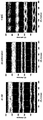
- FIG. 4 is a diagram showing simulated contour plots of normalized radiance intensity
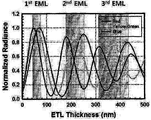
- FIG. 5 is a diagram showing normalized radiance according to an electron layer thickness. Is a diagram conceptually showing electron layer thicknesses in a three stack dendum structure.
- FIG. 7 and 8 are diagrams illustrating power efficiency and EL spectra of manufactured unit devices.
- the tandem organic light emitting device 100 includes a base substrate 110, a first electrode 120, a second electrode 130, and an organic light emitting layer. do.
- the base substrate 110 serves as a path for emitting light generated from the organic light emitting layer to the outside.
- the base substrate 110 is disposed in front of the organic light emitting layer, that is, a path through which light generated from the organic light emitting layer is emitted to the outside.
- the base substrate 110 serves to protect the first electrode 120, the second electrode 130, and the organic light emitting layer from the external environment.
- the base substrate 110 is formed along a rim thereof, for example, through a sealing material such as epoxy. It is bonded to a rear substrate (not shown) disposed on the second electrode 130 to face the second electrode 130.
- a space occupied by the first electrode 120, the second electrode 130, and the organic light emitting layer is formed among the internal spaces defined by the base substrate 110 and the rear substrate (not shown) facing each other and the sealing material formed at the edges thereof.
- the other inner space may be filled with an inert gas or be formed in a vacuum atmosphere.
- a separate external light extraction layer (not shown) is formed on the surface of the base substrate 110 in contact with the outside to improve the efficiency of extracting light emitted from the organic light emitting layer to the outside, or the surface itself forms a lens array shape. Can be.
- an internal light extraction layer (not shown) may be formed between the base substrate 110 and the first electrode 120.
- the base substrate 110 is a transparent substrate and is not limited as long as it has excellent light transmittance and excellent mechanical properties.
- a polymer-based material which is an organic film capable of thermosetting or UV curing may be used as the base substrate 110.
- the base substrate 110 is a chemically tempered glass of soda lime glass (SiO 2 -CaO-Na 2 O ) or alumino-silicate glass (SiO 2 -Al 2 O 3 -Na 2 O) may be used.
- soda-lime glass may be used as the base substrate 110.
- a substrate made of metal oxide or metal nitride may be used as the base substrate 110.
- a flexible substrate may be used as the base substrate 110.
- a thin glass having a thickness of 1.5 mm or less may be used. In this case, the thin glass may be manufactured through a fusion method or a floating method.
- a back substrate (not shown) forming encapsulation with the base substrate 110 may be made of the same or different material as that of the base substrate 110.
- the first electrode 120 is formed on the base substrate 110.
- the first electrode 120 is a transparent electrode which serves as an anode of the tandem organic light emitting diode 100 and is organic in a material having a high work function so that hole injection into the organic light emitting layer is easily performed.
- the light emitted from the light emitting layer may be made of a material that can transmit well.
- the first electrode 120 may be made of ITO.
- the second electrode 130 is formed to face the first electrode 120. Accordingly, a plurality of organic emission layers are positioned between the second electrode 130 and the first electrode 120.
- the second electrode 130 is a metal electrode serving as a cathode of the tandem organic light emitting device 100, and among the materials reflecting light emitted from the organic light emitting layer to the front, that is, the base substrate 110,
- the work function may be made of a material having a small work function to facilitate electron injection into the light emitting layer.
- the second electrode 130 may be formed of a metal thin film such as Al, Al: Li, or Mg: Ag.
- At least two organic light emitting layers are formed between the first electrode 120 and the second electrode 130 to form the tandem organic light emitting device 100.
- the tandem organic light emitting device 100 according to the embodiment of the present invention is formed including three organic light emitting layers. That is, in the tandem organic light emitting device 100 according to the embodiment of the present invention, the first organic light emitting layer 140 is sequentially formed from the first electrode 120 between the first electrode 120 and the second electrode 130. , The second organic light emitting layer 150 and the third organic light emitting layer 160 are formed.
- first organic light emitting layer 140 and the second organic light emitting layer 150 are connected through a first charge generation layer (CGL) 170 formed therebetween, and the second organic light emitting layer 150 ) And the third organic light emitting layer 160 are connected through the second charge generation layer 180 formed therebetween.
- CGL first charge generation layer
- the first organic emission layer 140 includes a first emission layer 141 that emits blue light.
- the first emission layer 141 may be formed of a material emitting blue light having a wavelength of 450 ⁇ 5 nm.
- the second organic emission layer 150 includes a second emission layer 151 emitting yellow light.
- the second light emitting layer 151 may be formed of a material emitting yellow light having a wavelength of 540 ⁇ 5 nm.
- the third organic light emitting layer 160 includes a third light emitting layer 161 emitting red light.
- the third emission layer 161 may be formed of a material that emits red light in a wavelength range of 610 ⁇ 5nm.
- the tandem organic light according to the embodiment of the present invention is produced by the mixing effect of the blue light, the yellow light, and the red light emitted from the first light emitting layer 141, the second light emitting layer 151, and the third light emitting layer 161, respectively.
- the light emitting device 100 emits white light.
- the tandem organic light emitting device 100 has a blue / yellow / red first to third light emitting layer (1) from the first electrode 120 when viewed from the first electrode 120.
- 141, 151, and 161 form a structure arranged in sequence.
- the distance between the second light emitting layer 151 and the third light emitting layer 161 is the distance between the first light emitting layer 141 and the second light emitting layer 151 and the third light emitting layer 161 and the third light emitting layer 161. It may be formed longer than the distance between the two electrodes (130).
- the distance between the second light emitting layer 151 and the third light emitting layer 161 may be 100 to 300 nm.
- each of the first light emitting layer 141, the second light emitting layer 151, the third light emitting layer 161, and the second electrode 130 may have a distance between them less than 100 nm. Further, in the embodiment of the present invention, the distance between the second electrode 130 and the first light emitting layer 141, the distance between the second electrode 130 and the second light emitting layer 151, the second electrode 130 and the third light emitting layer The distance between the 161 and the distance between the first light emitting layer 141 and the first electrode 120 is controlled to a predetermined range.
- the distance between the first electrode 120 and the second electrode 130 is 500 nm or less, the distance between the first light emitting layer 141 and the second electrode 130 is 292 nm and the second light emitting layer 151.
- the distance between the second electrode 130 is 200 nm, the distance between the third light emitting layer 161 and the second electrode 130 is 60 nm, and the distance between the first electrode 120 and the first light emitting layer 141 is 95 nm. Controlling to nm may be most desirable to improve device performance of the tandem organic light emitting device 100.
- the first light emitting layer 141 which emits blue light sequentially from the first electrode 120, and emits yellow light between the first electrode 120 and the second electrode 130.
- the second light emitting layer 151 and the third light emitting layer 161 emitting red light are arranged, and the distance between the light emitting layers 141, 151, 161 and the second electrode 130 is controlled.
- the arrangement of the light emitting layers 141, 151, and 161 is optimized, resulting in low operating voltage, high power efficiency, and excellent color rendering index (CRI). It can be implemented.
- the first organic emission layer 140 includes a hole layer 142 formed on one side of the first emission layer 141 and an electron layer 143 formed on the other side of the first emission layer 141.
- the second organic emission layer 150 includes a hole layer 152 formed on one side of the second emission layer 151 and an electron layer 153 formed on the other side of the second emission layer 151.
- the third organic emission layer 160 includes a hole layer 162 formed on one side of the third emission layer 161 and an electron layer 163 formed on the other side of the third emission layer 161.
- the hole layers 142, 152, and 162 are formed in the direction of the first electrode 120
- the electron layers 143, 153, and 163 are formed in the direction of the second electrode 130.
- each of the hole layers 142, 152, and 162 may have a stacked structure of a hole injection layer HIL and a hole transport layer HTL, and the hole transport layer HTL may be, for example, a p-type. It may be made of a multilayer structure including a hole transport layer.
- the electron layers 143, 153, and 163 may have a stacked structure of an electron injection layer EIL and an electron transport layer ETL, and the electron transport layer ETL may have a multilayer structure including, for example, an n-type electron transport layer. Can be done.
- the first organic emission layer 140 holes move from the first electrode 120 to the first emission layer 141 through the hole layer 142 and electrons from the first charge generation layer 170. Is moved to the first emission layer 141 through the electron layer 143.
- a third charge generation layer (not shown) may be formed between the first organic emission layer 140 and the first electrode 120, and between the third charge generation layer (not shown) and the first electrode 120.
- a hole injection layer HIL (not shown) may be formed therein. In this case, in the first organic emission layer 140, holes are injected from the first electrode 120 through the hole injection layer HIL, the third charge generation layer (not shown), and the hole layer 142. Will be moved to.
- the second organic light emitting layer 150 holes move from the first charge generation layer 170 to the second light emitting layer 151 through the hole layer 152, and from the second charge generation layer 180. Electrons move to the second emission layer 151 through the electron layer 153.
- the third organic emission layer 160 holes move from the second charge generation layer 180 to the third emission layer 161 through the hole layer 162, and electrons from the second electrode 130 are electrons.
- the third light emitting layer 163 is moved through the layer 163.
- Tandem organic light emitting device consisting of a laminated structure of anode electrode / hole layer / blue light emitting layer / electron layer / charge generating layer / hole layer / yellow light emitting layer / electron layer / charge generating layer / hole layer / red light emitting layer / electron layer / cathode electrode was produced.
- Tandem organic light emitting device consisting of a laminated structure of anode electrode / hole layer / yellow light emitting layer / electron layer / charge generating layer / hole layer / blue light emitting layer / electron layer / charge generating layer / hole layer / red light emitting layer / electron layer / cathode electrode was produced.
- Tandem organic light emitting device consisting of a laminated structure of anode electrode / hole layer / red light emitting layer / electron layer / charge generating layer / hole layer / yellow light emitting layer / electron layer / charge generating layer / hole layer / blue light emitting layer / electron layer / cathode electrode was produced.
- Tandem organic light emitting device consisting of a laminated structure of anode electrode / hole layer / yellow light emitting layer / electron layer / charge generating layer / hole layer / red light emitting layer / electron layer / charge generating layer / hole layer / blue light emitting layer / electron layer / cathode electrode was produced.
- Example 2 is a graph showing the EL spectrum of the tandem organic light emitting device according to Example 1, Comparative Example 1, Comparative Example 2 and Comparative Example 3 of the present invention.
- Table 1 which shows the operating voltage, power efficiency, CIE, and CRI of the tandem organic light emitting diode according to Example 1, Comparative Example 1, Comparative Example 2, and Comparative Example 3 showing such an EL spectrum
- Example 1 in which the light emitting layer, the yellow light emitting layer, and the red light emitting layer are arranged in sequence shows a slightly lower color rendering index (CRI) than Comparative Example 1 and Comparative Example 3, but the driving voltage is lower than that of Comparative Examples 1, 2, and 3, It was confirmed that the moonlight shows high power efficiency.
- CRI color rendering index
- the distance between the blue light emitting layer and the cathode electrode, the distance between the yellow light emitting layer and the cathode electrode, and the distance between the red light emitting layer and the cathode were 292 nm, 200 nm, and 60 nm, respectively. Controlled.
- the distance between the blue light emitting layer and the cathode electrode, the distance between the yellow light emitting layer and the cathode electrode, and the distance between the red light emitting layer and the cathode were 312 nm, 220 nm, and 60 nm, respectively. Controlled.
- the distance between the blue light emitting layer and the cathode electrode, the distance between the yellow light emitting layer and the cathode electrode, and the distance between the red light emitting layer and the cathode were 284 nm, 192 nm, and 60 nm, respectively. Controlled.
- the distance between the blue light emitting layer and the anode electrode was controlled to 95 nm.
- the distance between the blue light emitting layer and the anode electrode was controlled to 65 nm.
- the distance between the blue light emitting layer and the anode electrode was controlled to 125 nm.
- FIG 3 is a graph showing EL spectra of tandem organic light emitting diodes according to Example 3, Comparative Example 6, and Comparative Example 7 of the present invention.
- Table 3 which shows the operating voltage, power efficiency, CIE, and CRI of the tandem organic light emitting diode according to Example 3, Comparative Example 6, and Comparative Example 7, which show such an EL spectrum
- the distance between the blue light emitting layer and the anode electrode Example 3, which is controlled to 95 nm has a lower operating voltage than Comparative Example 6 and Comparative Example 7, and it is confirmed that there is no difference in power efficiency and color rendering index (CRI).
- the optimal arrangement of the light emitting layers in the tandem organic light emitting device is arranged from the anode electrode to the blue light emitting layer, the yellow light emitting layer and the red light emitting layer in turn, and the blue light emitting layer and the cathode electrode
- the distance between the yellow light emitting layer and the cathode, the distance between the red light emitting layer and the cathode was 292 nm, 200 nm, 60 nm and the distance between the blue light emitting layer and the anode electrode was 95 nm, respectively.
- FIG. 4 is a diagram illustrating simulated contour plots of normalized radiance intensity
- FIG. 5 is a diagram illustrating normalized radiance according to an electron layer thickness.
- phosphorescent red, yellow-green and fluorescent bluebottom emission unit devices Prior to fabricating three-stack tandem devices, phosphorescent red, yellow-green and fluorescent bluebottom emission unit devices before were fabricated. .
- the radiance distribution of the light emitting layer was simulated by varying the thickness of the electron and hole layers. As a result, it can be seen that the radiance distribution is more sensitive to the thickness of the electronic layer than the thickness of the hole layer.
- FIG. 7 and 8 are diagrams illustrating power efficiency and EL spectra of manufactured unit devices.
- Monochromatic OLEDs were produced. Their dimensions are as follows.
- ITO 150 nm
- p-hole layer 82 nm
- hole layer 43 nm
- R-light emitting layer 15 nm
- electron layer 10 nm
- n-electron layer 50 nm
- Al 100 nm
- Device YG (Yello-Green): ITO (150 nm) / p-hole layer (82 nm) / hole layer (43 nm) / YG- light emitting layer (15 nm) / electron layer (10 nm) / n-electron layer ( 40 nm) / Al (100 nm).
- Device B (Blue): ITO (150 nm) / p-hole layer (40 nm) / hole layer (25 nm) / B-light emitting layer (15 nm) / electron layer (10 nm) / n-electron layer (20 nm ) / Al (100 nm).
- the normalized unit spectra can be superimposed to calculate the EL spectrum of the tandem device.
- tandem organic light emitting device 110 base substrate
- first organic light emitting layer 141 first light emitting layer
- first charge generation layer 180 second charge generation layer
Landscapes
- Physics & Mathematics (AREA)
- Optics & Photonics (AREA)
- Electroluminescent Light Sources (AREA)
Abstract
본 발명은 탠덤형 유기발광소자에 관한 것으로서 더욱 상세하게는 낮은 동작전압 및 높은 전력효율 그리고 우수한 연색지수(CRI)를 나타내는 탠덤형 유기발광소자에 관한 것이다. 이를 위해, 본 발명은, 베이스 기판; 상기 베이스 기판 상에 형성되는 제1 전극; 상기 제1 전극과 대향되게 형성되는 제2 전극; 상기 제1 전극과 상기 제2 전극 사이에 상기 제1 전극으로부터 차례로 형성되는 제1 내지 제3 유기 발광층을 포함하되, 상기 제1 유기 발광층은 청색 광을 발광하는 제1 발광층을 포함하고, 상기 제2 유기 발광층은 황색 광을 발광하는 제2 발광층을 포함하며, 상기 제3 유기 발광층은 적색 광을 발광하는 제3 발광층을 포함하는 것을 특징으로 하는 탠덤형 유기발광소자를 제공한다.
Description
본 발명은 탠덤형 유기발광소자에 관한 것으로서 더욱 상세하게는 낮은 동작전압 및 높은 전력효율 그리고 우수한 연색지수(CRI)를 나타내는 탠덤형 유기발광소자에 관한 것이다.
최근, 디스플레이 및 조명 장치는 경량화, 박막화, 고효율화 및 친환경성 등을 요구 받고 있는데, 이러한 요구에 부흥하기 위하여, 유기발광소자를 이용한 연구가 이루어지고 있다.
이러한 유기발광소자는 유기 발광층의 구성 방법에 따라, 하나의 유기 발광층으로 구성된 단일형과 두 개 이상의 유기 발광층이 직렬로 적층된 탠덤형으로 구분된다. 이중, 탠덤형 유기발광소자는 단일형 유기발광소자에 비하여 높은 안정성과 긴 수명을 갖는 장점이 있어, 고 휘도 및 긴 수명을 요구하는 디스플레이 장치나 조명 장치에 사용될 수 있다.
한편, 백색 유기발광소자는 양극과 음극 사이에 복수의 색상의 광을 발광하는 서로 다른 유기 발광층을 구비한다. 이때, 각각의 유기 발광층 사이에는 전하 생성층(charge generation layer)이 형성된다. 이때, 별도의 기능을 갖는 구성 추가 없이 유기발광소자의 전력효율, 연색지수(CRI)와 같은 소자 특성을 향상시키기 위해서는 각각의 유기 발광층 간의 배열 순서 및 양극 또는 음극과 유기 발광층 간의 거리를 최적화할 필요가 있다.
[선행기술문헌]
일본 등록특허공보 제4649676호(2010.12.24.)
본 발명은 상술한 바와 같은 종래기술의 문제점을 해결하기 위해 안출된 것으로서, 본 발명의 목적은 낮은 동작전압 및 높은 전력효율 그리고 우수한 연색지수(CRI)를 나타내는 탠덤형 유기발광소자를 제공하는 것이다.
이를 위해, 본 발명은, 베이스 기판; 상기 베이스 기판 상에 형성되는 제1 전극; 상기 제1 전극과 대향되게 형성되는 제2 전극; 상기 제1 전극과 상기 제2 전극 사이에 상기 제1 전극으로부터 차례로 형성되는 제1 내지 제3 유기 발광층을 포함하되, 상기 제1 유기 발광층은 청색 광을 발광하는 제1 발광층을 포함하고, 상기 제2 유기 발광층은 황색 광을 발광하는 제2 발광층을 포함하며, 상기 제3 유기 발광층은 적색 광을 발광하는 제3 발광층을 포함하는 것을 특징으로 하는 탠덤형 유기발광소자를 제공한다.
여기서, 상기 제2 발광층과 상기 제3 발광층 사이의 거리는 상기 제1 발광층과 상기 제2 발광층 사이의 거리 및 상기 제3 발광층과 상기 제2 전극 사이의 거리보다 길 수 있다.
이때, 상기 제2 발광층과 상기 제3 발광층 사이의 거리는 100~300㎚일 수 있다.
또한, 상기 제1 발광층과 상기 제2 발광층 사이의 거리 및 상기 제3 발광층과 상기 제2 전극 사이의 거리는 100㎚ 미만일 수 있다.
그리고 상기 제1 전극과 상기 제2 전극 사이의 거리가 500㎚ 이하일 때, 상기 제1 발광층과 상기 제2 전극 사이의 거리는 292㎚, 상기 제2 발광층과 상기 제2 전극 사이의 거리는 200㎚, 상기 제3 발광층과 상기 제2 전극 사이의 거리는 60㎚, 상기 제1 전극과 상기 제1 발광층 사이의 거리는 95㎚일 수 있다.
아울러, 상기 제1 유기 발광층과 상기 제2 유기 발광층 사이에 형성되는 제1 전하 생성층 및 상기 제2 유기 발광층과 상기 제3 유기 발광층 사이에 형성되는 제2 전하 생성층을 더 포함할 수 있다.
이때, 상기 제1 발광층과 상기 제1 전극 사이에 형성되는 제3 전하 생성층을 더 포함할 수 있다.
또한, 상기 제1 내지 제3 발광층 각각의 일측에는 정공층이 형성되고, 타측에는 전자층이 형성되되, 상기 정공층은 상기 제1 전극 방향에 형성되고, 상기 전자층은 상기 제2 전극 방향에 형성될 수 있다.
그리고 상기 베이스 기판은 플렉서블 기판으로 이루어질 수 있다.
이때, 상기 베이스 기판은 두께 1.5㎜ 이하의 박판 유리로 이루어질 수 있다.
본 발명에 따르면, 애노드 전극과 캐소드 전극 사이에 배치되는 청색 발광층, 황색 발광층 및 적색 발광층의 배열 순서, 발광층들과 캐소드 전극 또는 발광층들과 애노드 전극 사이의 거리 및 발광층들 사이의 거리를 제어하여, 발광층들의 배치구조를 최적화함으로써, 탠덤형 유기발광소자의 동작전압을 낮출 수 있고, 이를 통해, 전력효율을 높일 수 있음과 아울러, 탠덤형 유기발광소자의 연색지수(CRI)를 향상시킬 수 있다.
도 1은 본 발명의 실시 예에 따른 탠덤형 유기발광소자의 구조를 개략적으로 나타낸 단면 모식도.
도 2는 본 발명의 실시 예1, 비교 예1, 비교 예2 및 비교 예3에 따른 탠덤형 유기발광소자의 EL 스펙트럼을 나타낸 그래프.
도 3은 본 발명의 실시 예3, 비교 예6 및 비교 예7에 따른 탠덤형 유기발광소자들의 EL 스펙트럼을 나타낸 그래프.
도 4는 정규화된 라디언스 인텐서티(normalized radiance intensity)의 시뮬레이션등고선(Simulated contour plots of normalized radiance intensity)을 보여주는 도면이고, 도 5는 전자층 두께에 따른 정규화된 라디언스를 보여주는 도면이고, 도 6은 3 스택 덴덤 구조에서 전자층 두께들을 개념적으로 보여주는 도면이다.
도 7 및 도 8은 제작된 유닛 디바이스들의 전력효율(Power efficiency) 및 EL 스펙트럼(EL spectra)을 보여주는 도면이다.
이하에서는 첨부된 도면들을 참조하여 본 발명의 실시 예에 따른 탠덤형 유기발광소자에 대해 상세히 설명한다.
아울러, 본 발명을 설명함에 있어서, 관련된 공지 기능 혹은 구성에 대한 구체적인 설명이 본 발명의 요지를 불필요하게 흐릴 수 있다고 판단된 경우 그 상세한 설명은 생략한다.
도 1에 도시한 바와 같이, 본 발명의 실시 예에 따른 탠덤형 유기발광소자(100)는 베이스 기판(110), 제1 전극(120), 제2 전극(130) 및 유기 발광층을 포함하여 형성된다.
베이스 기판(110)은 유기 발광층으로부터 발생된 광을 외부로 방출시키는 통로 역할을 한다. 이를 위해, 베이스 기판(110)은 유기 발광층의 전방, 즉, 유기 발광층으로부터 발생된 광이 외부로 방출되는 경로에 배치된다. 또한, 베이스 기판(110)은 제1 전극(120), 제2 전극(130) 및 유기 발광층을 외부 환경으로부터 보호하는 역할을 한다. 이를 위해, 즉, 제1 전극(120), 제2 전극(130) 및 유기 발광층을 인캡슐레이션 시키기 위해, 베이스 기판(110)은 이의 테두리를 따라 형성되는 예컨대, 에폭시와 같은 씰링재를 매개로, 제2 전극(130) 상부에 이와 대향되게 배치되는 후면 기판(미도시)과 접합된다. 이때, 서로 대향되는 베이스 기판(110) 및 후면 기판(미도시) 그리고 이들 테두리에 형성되는 씰링재에 의해 구획되는 내부 공간 중 제1 전극(120), 제2 전극(130) 및 유기 발광층이 차지하는 공간 이외의 내부 공간은 불활성 기체로 채워지거나 진공 분위기로 조성될 수 있다.
한편, 베이스 기판(110)에서 외기와 접하는 표면에는 유기 발광층으로부터 방출된 광을 외부로 추출하는 효율을 향상시키기 위한 별도의 외부 광추출층(미도시)이 형성되거나 표면 자체가 렌즈 어레이 형상을 이룰 수 있다. 또한, 베이스 기판(110)과 제1 전극(120) 사이에는 내부 광추출층(미도시)이 형성될 수도 있다.
이러한 베이스 기판(110)은 투명 기판으로, 광 투과율이 우수하고 기계적인 물성이 우수한 것이면 어느 것이든 제한되지 않는다. 예를 들어, 베이스 기판(110)으로는 열경화 또는 UV 경화가 가능한 유기필름인 고분자 계열의 물질이 사용될 수 있다. 또한, 베이스 기판(110)으로는 화학강화유리인 소다라임 유리(SiO2-CaO-Na2O) 또는 알루미노실리케이트계 유리(SiO2-Al2O3-Na2O)가 사용될 수 있다. 여기서, 본 발명의 실시 예에 따른 탠덤형 유기발광소자(100)가 조명용인 경우, 베이스 기판(110)으로는 소다라임 유리가 사용될 수 있다. 이외에도 베이스 기판(110)으로는 금속산화물이나 금속질화물로 이루어진 기판이 사용될 수도 있다. 그리고 본 발명의 실시 예에서는 베이스 기판(110)으로 플렉서블(flexible) 기판이 사용될 수 있는데, 특히, 두께 1.5㎜ 이하의 박판 유리가 사용될 수 있다. 이때, 이러한 박판 유리는 퓨전(fusion) 공법 또는 플로팅(floating) 공법을 통해 제조될 수 있다. 한편, 베이스 기판(110)과 인캡슐레이션을 이루는 후면 기판(미도시)은 베이스 기판(110)과 동일 또는 다른 물질로 이루어질 수 있다.
제1 전극(120)은 베이스 기판(110) 상에 형성된다. 이러한 제1 전극(120)은 탠덤형 유기발광소자(100)의 애노드(anode)로서의 역할을 하는 투명전극으로, 유기 발광층으로의 정공 주입이 잘 일어나도록 일함수(work function)가 큰 물질 중 유기 발광층에서 발광된 빛이 잘 투과될 수 있는 물질로 이루어질 수 있다. 예를 들어, 제1 전극(120)은 ITO로 이루어질 수 있다.
제2 전극(130)은 제1 전극(120)과 대향되게 형성된다. 이에 따라, 제2 전극(130)과 제1 전극(120) 사이에는 복수 개의 유기 발광층이 위치하게 된다. 이러한 제2 전극(130)은 탠덤형 유기발광소자(100)의 캐소드(cathode)로서의 역할을 하는 금속전극으로, 유기 발광층으로부터 발광된 빛을 전방 즉, 베이스 기판(110) 측으로 반사시키는 물질 중 유기 발광층으로의 전자 주입이 잘 일어나도록 일함수가 작은 물질로 이루어질 수 있다. 예를 들어, 제2 전극(130)은 Al, Al:Li 또는 Mg:Ag와 같은 금속 박막으로 이루어질 수 있다.
유기 발광층은 탠덤형 유기발광소자(100)를 이루기 위해, 제1 전극(120)과 제2 전극(130) 사이에 적어도 2개 이상 형성된다. 본 발명의 실시 예에 따른 탠덤형 유기발광소자(100)는 3개의 유기 발광층을 포함하여 형성된다. 즉, 본 발명의 실시 예에 따른 탠덤형 유기발광소자(100)는 제1 전극(120)과 제2 전극(130) 사이에 제1 전극(120)으로부터 차례로 형성되는 제1 유기 발광층(140), 제2 유기 발광층(150) 및 제3 유기 발광층(160)을 포함하여 형성된다. 이때, 제1 유기 발광층(140)과 제2 유기 발광층(150)은 이들 사이에 형성되는 제1 전하 생성층(charge generation layer; CGL)(170)을 매개로 연결되고, 제2 유기 발광층(150)과 제3 유기 발광층(160)은 이들 사이에 형성되는 제2 전하 생성층(180)을 매개로 연결된다.
본 발명의 실시 예에서, 제1 유기 발광층(140)은 청색 광을 발광하는 제1 발광층(141)을 포함한다. 이때, 제1 발광층(141)은 450±5㎚ 파장대의 청색 광을 방출하는 물질로 이루어질 수 있다. 또한, 제2 유기 발광층(150)은 황색 광을 발광하는 제2 발광층(151)을 포함한다. 이때, 제2 발광층(151)은 540±5㎚ 파장대의 황색 광을 방출하는 물질로 이루어질 수 있다. 그리고 제3 유기 발광층(160)은 적색 광을 발광하는 제3 발광층(161)을 포함한다. 이때, 제3 발광층(161)은 610±5㎚ 파장대의 적색 광을 방출하는 물질로 이루어질 수 있다. 이와 같이, 제1 발광층(141), 제2 발광층(151) 및 제3 발광층(161)으로부터 각각 방출되는 청색 광, 황색 광 및 적색 광의 혼합 효과에 의해, 본 발명의 실시 예에 따른 탠덤형 유기발광소자(100)는 백색 광을 방출하게 된다.
여기서, 본 발명의 실시 예에 따른 탠덤형 유기발광소자(100)는 제1 전극(120)을 기준으로 볼 때, 제1 전극(120)으로부터 청색/황색/적색의 제1 내지 제3 발광층(141, 151, 161)이 차례로 배열된 구조를 이룬다. 이때, 본 발명의 실시 예에서는 제2 발광층(151)과 제3 발광층(161) 사이의 거리가 제1 발광층(141)과 제2 발광층(151) 사이의 거리 및 제3 발광층(161)과 제2 전극(130) 사이의 거리보다 길게 형성될 수 있다. 예를 들어, 제2 발광층(151)과 제3 발광층(161)은, 그 사이 거리가 100~300㎚로 형성될 수 있다. 이 경우, 제1 발광층(141)과 제2 발광층(151) 및 제3 발광층(161)과 제2 전극(130) 각각은, 그 사이 거리가 100㎚ 미만으로 형성될 수 있다. 또한, 본 발명의 실시 예에서는 제2 전극(130)과 제1 발광층(141) 간의 거리, 제2 전극(130)과 제2 발광층(151) 간의 거리, 제2 전극(130)과 제3 발광층(161) 간의 거리 및 제1 발광층(141)과 제1 전극(120) 사이의 거리를 소정 범위로 제어한다. 예를 들어, 제1 전극(120)과 제2 전극(130) 사이의 거리가 500㎚ 이하인 경우, 제1 발광층(141)과 제2 전극(130) 사이의 거리는 292㎚, 제2 발광층(151)과 제2 전극(130) 사이의 거리는 200㎚, 제3 발광층(161)과 제2 전극(130) 사이의 거리는 60㎚, 제1 전극(120)과 제1 발광층(141) 사이의 거리는 95㎚로 제어되는 것이 탠덤형 유기발광소자(100)의 소자 성능을 향상시키는데 가장 바람직할 수 있다.
이와 같이, 본 발명의 실시 예에서는 제1 전극(120)과 제2 전극(130) 사이에, 제1 전극(120)으로부터 차례로 청색 광을 발광하는 제1 발광층(141), 황색 광을 발광하는 제2 발광층(151) 및 적색 광을 발광하는 제3 발광층(161)을 배열하고, 각 발광층들(141, 151, 161)과 제2 전극(130) 사이의 거리를 제어한다. 이를 통해, 본 발명의 실시 예에 따른 탠덤형 유기발광소자(100)는 발광층들(141, 151, 161)의 배치구조가 최적화되어, 낮은 동작전압, 높은 전력효율 그리고 우수한 연색지수(CRI)를 구현할 수 있게 된다.
한편, 제1 유기 발광층(140)은 제1 발광층(141)의 일측에 형성되는 정공층(142) 및 제1 발광층(141)의 타측에 형성되는 전자층(143)을 포함한다. 또한, 제2 유기 발광층(150)은 제2 발광층(151)의 일측에 형성되는 정공층(152) 및 제2 발광층(151)의 타측에 형성되는 전자층(153)을 포함한다. 그리고 제3 유기 발광층(160)은 제3 발광층(161)의 일측에 형성되는 정공층(162) 및 제3 발광층(161)의 타측에 형성되는 전자층(163)을 포함한다. 이때, 정공층(142, 152, 162)은 제1 전극(120) 방향에 형성되고, 전자층(143, 153, 163)은 제2 전극(130) 방향에 형성된다.
여기서, 구체적으로 도시하진 않았지만, 각각의 정공층(142, 152, 162)은 정공 주입층(HIL)과 정공 수송층(HTL)의 적층 구조로 이루어질 수 있고, 정공 수송층(HTL)은 예컨대, p형 정공 수송층을 포함하는 다층 구조로 이루어질 수 있다. 또한, 전자층(143, 153, 163)은 전자 주입층(EIL)과 전자 수송층(ETL)의 적층 구조로 이루어질 수 있고, 전자 수송층(ETL)은 예컨대, n형 전자 수송층을 포함하는 다층 구조로 이루어질 수 있다.
이에 따라, 제1 유기 발광층(140)의 경우에는 제1 전극(120)으로부터 정공이 정공층(142)을 통해 제1 발광층(141)으로 이동하게 되고, 제1 전하 생성층(170)으로부터 전자가 전자층(143)을 통해 제1 발광층(141)으로 이동하게 된다. 이때, 제1 유기 발광층(140)과 제1 전극(120) 사이에는 제3 전하 생성층(미도시)이 형성될 수 있고, 제3 전하 생성층(미도시)과 제1 전극(120) 사이에는 정공 주입층(HIL)(미도시)이 형성될 수 있다. 이 경우, 제1 유기 발광층(140)에서는 제1 전극(120)으로부터 정공이 정공 주입층(HIL), 제3 전하 생성층(미도시) 및 정공층(142)을 통해 제1 발광층(141)으로 이동하게 된다. 또한, 제2 유기 발광층(150)의 경우에는 제1 전하 생성층(170)으로부터 정공이 정공층(152)을 통해 제2 발광층(151)으로 이동하게 되고, 제2 전하 생성층(180)으로부터 전자가 전자층(153)을 통해 제2 발광층(151)으로 이동하게 된다. 그리고 제3 유기 발광층(160)의 경우에는 제2 전하 생성층(180)으로부터 정공이 정공층(162)을 통해 제3 발광층(161)으로 이동하게 되고, 제2 전극(130)으로부터 전자가 전자층(163)을 통해 제3 발광층(163)으로 이동하게 된다.
제1 전극(120) 및 제2 전극(130)에 순방향 전압이 인가되면, 상기와 같은 경로를 통해 전자와 정공이 각각의 발광층(141, 151, 161)으로 이동하게 된다. 이와 같이, 각각의 발광층(141, 151, 161) 내로 주입된 전자와 정공은 각각의 발광층(141, 151, 161)에서 재결합하여 엑시톤(exciton)을 생성하고, 이러한 엑시톤이 여기상태(excited state)에 기저상태(ground state)로 전이하면서 빛을 방출하게 되는데, 이때, 방출되는 빛의 밝기는 애노드 전극으로 작용하는 제1 전극(120)과 캐소드 전극으로 작용하는 제2 전극(130) 사이에 흐르는 전류량에 비례하게 된다.
실시 예1
애노드 전극/정공층/청색 발광층/전자층/전하 생성층/정공층/황색 발광층/전자층/전하 생성층/정공층/적색 발광층/전자층/캐소드 전극의 적층 구조로 이루어진 탠덤형 유기발광소자를 제작하였다.
비교 예1
애노드 전극/정공층/황색 발광층/전자층/전하 생성층/정공층/청색 발광층/전자층/전하 생성층/정공층/적색 발광층/전자층/캐소드 전극의 적층 구조로 이루어진 탠덤형 유기발광소자를 제작하였다.
비교 예2
애노드 전극/정공층/적색 발광층/전자층/전하 생성층/정공층/황색 발광층/전자층/전하 생성층/정공층/청색 발광층/전자층/캐소드 전극의 적층 구조로 이루어진 탠덤형 유기발광소자를 제작하였다.
비교 예3
애노드 전극/정공층/황색 발광층/전자층/전하 생성층/정공층/적색 발광층/전자층/전하 생성층/정공층/청색 발광층/전자층/캐소드 전극의 적층 구조로 이루어진 탠덤형 유기발광소자를 제작하였다.
| @3,000nit | 실시 예1 | 비교 예1 | 비교 예2 | 비교 예3 |
| 동작전압(V) | 10.2 | 10.9 | 10.5 | 12.3 |
| 전력효율(lm/W) | 25.6 | 14.2 | 17.5 | 6.1 |
| CIE(x, y) | (0.453, 0.463) | (0.424, 0.393) | (0.453, 0.463) | (0.362, 0.374) |
| CRI | 75.4 | 88.5 | 41.9 | 85.9 |
도 2는 본 발명의 실시 예1, 비교 예1, 비교 예2 및 비교 예3에 따른 탠덤형 유기발광소자의 EL 스펙트럼을 나타낸 그래프이다. 이와 같은 EL 스펙트럼을 나타내는 실시 예1, 비교 예1, 비교 예2 및 비교 예3에 따른 탠덤형 유기발광소자의 동작전압, 전력효율, CIE, CRI를 나타낸 상기의 표 1을 보면, 애노드로부터 청색 발광층, 황색 발광층 및 적색 발광층이 차례로 배열되어 있는 실시 예1은 비교 예1 및 비교 예3보다 연색지수(CRI)는 약간 낮은 값을 나타내지만, 비교 예1,2,3보다 구동전압이 낮고, 월등이 높은 전력효율을 나타내는 것으로 확인되었다.
실시 예2
실시 예1과 동일한 구조의 탠덤형 유기발광소자에서, 청색 발광층과 캐소드 전극 사이의 거리, 황색 발광층과 캐소드 전극 사이의 거리, 적색 발광층과 캐소드 사이의 거리를 각각, 292㎚, 200㎚, 60㎚로 제어하였다.
비교 예4
실시 예1과 동일한 구조의 탠덤형 유기발광소자에서, 청색 발광층과 캐소드 전극 사이의 거리, 황색 발광층과 캐소드 전극 사이의 거리, 적색 발광층과 캐소드 사이의 거리를 각각, 312㎚, 220㎚, 60㎚로 제어하였다.
비교 예5
실시 예1과 동일한 구조의 탠덤형 유기발광소자에서, 청색 발광층과 캐소드 전극 사이의 거리, 황색 발광층과 캐소드 전극 사이의 거리, 적색 발광층과 캐소드 사이의 거리를 각각, 284㎚, 192㎚, 60㎚로 제어하였다.
| @3,000nit | 실시 예2 | 비교 예4 | 비교 예5 |
| 동작전압(V) | 9.62 | 10.6 | 9.84 |
| 전력효율(lm/W) | 44.9 | 22.7 | 34.4 |
| CIE(x, y) | (0.465, 0.448) | (0.508, 0.438) | (0.448, 0.455) |
| CRI | 80.5 | 75.5 | 75.0 |
본 발명의 실시 예2, 비교 예4 및 비교 예5에 따른 탠덤형 유기발광소자의 동작전압, 전력효율, CIE, CRI를 나타낸 상기 표 2를 보면, 청색 발광층과 캐소드 전극 사이의 거리, 황색 발광층과 캐소드 전극 사이의 거리, 적색 발광층과 캐소드 사이의 거리를 각각, 292㎚, 200㎚, 60㎚로 제어한 실시 예1은 비교 예4 및 비교 예 5보다 구동전압이 낮고, 월등히 높은 전력효율을 나타내는 것으로 확인되었고, 연색지수(CRI) 또한 상대적으로 우수한 것으로 확인되었다.
실시 예3
실시 예2와 동일한 구조의 탠덤형 유기발광소자에서, 청색 발광층과 애노드 전극 사이의 거리를 95㎚로 제어하였다.
비교 예6
실시 예2와 동일한 구조의 탠덤형 유기발광소자에서, 청색 발광층과 애노드 전극 사이의 거리를 65㎚로 제어하였다.
비교 예7
실시 예2와 동일한 구조의 탠덤형 유기발광소자에서, 청색 발광층과 애노드 전극 사이의 거리를 125㎚로 제어하였다.
| @3,000nit | 실시 예3 | 비교 예6 | 비교 예7 |
| 동작전압(V) | 8.34 | 8.51 | 8.51 |
| 전력효율(lm/W) | 43.5 | 44.5 | 43.8 |
| CIE(x, y) | (0.427, 0.450) | (0.420, 0.465) | (0.436, 0.448) |
| CRI | 81.9 | 79.3 | 85.8 |
도 3은 본 발명의 실시 예3, 비교 예6 및 비교 예7에 따른 탠덤형 유기발광소자들의 EL 스펙트럼을 나타낸 그래프이다. 이와 같은 EL 스펙트럼을 나타내는 실시 예3, 비교 예6 및 비교 예7에 따른 탠덤형 유기발광소자의 동작전압, 전력효율, CIE, CRI를 나타낸 상기 표 3을 보면, 청색 발광층과 애노드 전극 사이의 거리를 95㎚로 제어한 실시 예3은 비교 예6 및 비교 예7보다 동작전압이 낮고, 전력효율이나 연색지수(CRI)는 별다른 차이가 없는 것으로 확인되었다.
실시 예1 내지 3 및 비교 예1 내지 7을 종합해 보면, 탠덤형 유기발광소자에서 발광층들의 최적의 배치구조는 애노드 전극으로부터 청색 발광층, 황색 발광층 및 적색 발광층이 차례로 배열되고, 청색 발광층과 캐소드 전극 사이의 거리, 황색 발광층과 캐소드 전극 사이의 거리, 적색 발광층과 캐소드 사이의 거리가 각각, 292㎚, 200㎚, 60㎚ 및 청색 발광층과 애노드 전극 사이의 거리가 95㎚인 것으로 확인되었다.
도 4는 정규화된 라디언스 인텐서티(normalized radiance intensity)의 시뮬레이션등고선(Simulated contour plots of normalized radiance intensity)을 보여주는 도면이고, 도 5는 전자층 두께에 따른 정규화된 라디언스를 보여주는 도면이다.
3-스택 텐덤 장치(three-stack tandem devices)를 제작하기에 앞서, 인광 레드, 엘로우-그린 및 형광 블루의 바텀 이미션 유닛 장치(phosphorescent red, yellow-green and fluorescent bluebottom emissionunit devices before)들을 제작하였다. 전자층 및 정공층의 두께를 변화시켜 가면서 발광층의 라디언스 분포를 시뮬레이션 하였다. 그 결과, 도시한 바와 같이, 라디언스 분포는 정공층의 두께보다 전자층의 두께에 더 민감함을 알 수 있었다.
도 6은 3-스택 덴덤 구조에서 전자층 두께들을 개념적으로 보여주는 도면이다.
도 7 및 도 8은 제작된 유닛 디바이스들의 전력효율(Power efficiency) 및 EL 스펙트럼(EL spectra)를 보여주는 도면이다.
단색 OLED들을 제작하였다. 이들의 치수는 다음과 같다.
장치 R (Red): ITO (150 nm)/ p-정공층 (82 nm)/ 정공층 (43 nm)/ R-발광층 (15 nm)/ 전자층 (10 nm)/ n-전자층 (50 nm)/ Al (100 nm).
장치 YG (Yello-Green): ITO (150 nm)/ p-정공층 (82 nm)/ 정공층 (43 nm)/ YG-발광층 (15 nm)/ 전자층 (10 nm)/ n-전자층 (40 nm)/ Al (100 nm).
장치 B (Blue): ITO (150 nm)/ p-정공층 (40 nm)/ 정공층 (25 nm)/ B-발광층 (15 nm)/ 전자층 (10 nm)/ n-전자층 (20 nm)/ Al (100 nm).
도 7에 도시한 바와 같이, 장치 R (2.5V), 장치 YG (2.5V) 및 장치 B (2.9V) 각각에 대해서, 40.6 lm/W (22.8 %), 109.4 lm/W (24.0 %), 및 8.7 lm/W (5.1 %)의 전력효율을 얻을 수 있었다. 이러한 결과로부터, 유닛들의 연결(interconnecting)에 기인하는 전기적 및 광학적 손실이 없다는 전제하에, 3-스택 텐덤 백색 장치의 전력효율을 예측할 수 있다. 3-스택 백색 장치의 계산된 PE(Power Efficiency) 및 EQE(External Quantum Efficiency)는 휘도 1000 nit (7.5V)에서 55 lm/W 및 52%이다.
도 8에 도시한 바와 같이, 정규화된 유닛 스펙트럼들을 겹치게 하여, 텐덤 장치의 EL 스펙트럼을 계산할 수 있다.
이상과 같이 본 발명은 비록 한정된 실시 예와 도면에 의해 설명되었으나, 본 발명은 상기의 실시 예에 한정되는 것은 아니며, 본 발명이 속하는 분야에서 통상의 지식을 가진 자라면 이러한 기재로부터 다양한 수정 및 변형이 가능하다.
그러므로 본 발명의 범위는 설명된 실시 예에 국한되어 정해져서는 아니 되며, 후술하는 특허청구범위뿐만 아니라 특허청구범위와 균등한 것들에 의해 정해져야 한다.
[부호의 설명]
100: 탠덤형 유기발광소자 110: 베이스 기판
120: 제1 전극 130: 제2 전극
140: 제1 유기 발광층 141: 제1 발광층
150: 제2 유기 발광층 151: 제2 발광층
160: 제3 유기 발광층 161: 제3 발광층
170: 제1 전하 생성층 180: 제2 전하 생성층
142, 152, 162: 정공층 143, 153, 163: 전자층
Claims (10)
- 베이스 기판;상기 베이스 기판 상에 형성되는 제1 전극;상기 제1 전극과 대향되게 형성되는 제2 전극;상기 제1 전극과 상기 제2 전극 사이에 상기 제1 전극으로부터 차례로 형성되는 제1 내지 제3 유기 발광층을 포함하되,상기 제1 유기 발광층은 청색 광을 발광하는 제1 발광층을 포함하고, 상기 제2 유기 발광층은 황색 광을 발광하는 제2 발광층을 포함하며, 상기 제3 유기 발광층은 적색 광을 발광하는 제3 발광층을 포함하는 것을 특징으로 하는 탠덤형 유기발광소자.
- 제1항에 있어서,상기 제2 발광층과 상기 제3 발광층 사이의 거리는 상기 제1 발광층과 상기 제2 발광층 사이의 거리 및 상기 제3 발광층과 상기 제2 전극 사이의 거리보다 긴 것을 특징으로 하는 탠덤형 유기발광소자.
- 제2항에 있어서,상기 제2 발광층과 상기 제3 발광층 사이의 거리는 100~300㎚인 것을 특징으로 하는 탠덤형 유기발광소자.
- 제3항에 있어서,상기 제1 발광층과 상기 제2 발광층 사이의 거리 및 상기 제3 발광층과 상기 제2 전극 사이의 거리는 100㎚ 미만인 것을 특징으로 하는 탠덤형 유기발광소자.
- 제1항에 있어서,상기 제1 전극과 상기 제2 전극 사이의 거리가 500㎚ 이하일 때, 상기 제1 발광층과 상기 제2 전극 사이의 거리는 292㎚, 상기 제2 발광층과 상기 제2 전극 사이의 거리는 200㎚, 상기 제3 발광층과 상기 제2 전극 사이의 거리는 60㎚, 상기 제1 전극과 상기 제1 발광층 사이의 거리는 95㎚인 것을 특징으로 하는 탠덤형 유기발광소자.
- 제1항에 있어서,상기 제1 유기 발광층과 상기 제2 유기 발광층 사이에 형성되는 제1 전하 생성층 및 상기 제2 유기 발광층과 상기 제3 유기 발광층 사이에 형성되는 제2 전하 생성층을 더 포함하는 것을 특징으로 하는 탠덤형 유기발광소자.
- 제6항에 있어서,상기 제1 유기 발광층과 상기 제1 전극 사이에 형성되는 제3 전하 생성층을 더 포함하는 것을 특징으로 하는 탠덤형 유기발광소자.
- 제1항에 있어서,상기 제1 내지 제3 발광층 각각의 일측에는 정공층이 형성되고, 타측에는 전자층이 형성되되,상기 정공층은 상기 제1 전극 방향에 형성되고, 상기 전자층은 상기 제2 전극 방향에 형성되는 것을 특징으로 하는 탠덤형 유기발광소자.
- 제1항에 있어서,상기 베이스 기판은 플렉서블 기판으로 이루어진 것을 특징으로 하는 탠덤형 유기발광소자.
- 제9항에 있어서,상기 베이스 기판은 두께 1.5㎜ 이하의 박판 유리로 이루어진 것을 특징으로 하는 탠덤형 유기발광소자.
Priority Applications (1)
| Application Number | Priority Date | Filing Date | Title |
|---|---|---|---|
| US15/541,647 US20180166644A1 (en) | 2015-01-05 | 2016-01-05 | Tandem type organic light emitting device |
Applications Claiming Priority (4)
| Application Number | Priority Date | Filing Date | Title |
|---|---|---|---|
| KR10-2015-0000399 | 2015-01-05 | ||
| KR20150000399 | 2015-01-05 | ||
| KR1020150071976A KR20160084282A (ko) | 2015-01-05 | 2015-05-22 | 탠덤형 유기발광소자 |
| KR10-2015-0071976 | 2015-05-22 |
Publications (1)
| Publication Number | Publication Date |
|---|---|
| WO2016111534A1 true WO2016111534A1 (ko) | 2016-07-14 |
Family
ID=56356166
Family Applications (1)
| Application Number | Title | Priority Date | Filing Date |
|---|---|---|---|
| PCT/KR2016/000073 Ceased WO2016111534A1 (ko) | 2015-01-05 | 2016-01-05 | 탠덤형 유기발광소자 |
Country Status (1)
| Country | Link |
|---|---|
| WO (1) | WO2016111534A1 (ko) |
Cited By (1)
| Publication number | Priority date | Publication date | Assignee | Title |
|---|---|---|---|---|
| CN112242429A (zh) * | 2020-10-20 | 2021-01-19 | 安徽熙泰智能科技有限公司 | 一种顶发射硅基oled器件结构以及显示方法 |
Citations (5)
| Publication number | Priority date | Publication date | Assignee | Title |
|---|---|---|---|---|
| JP2006332049A (ja) * | 2005-05-20 | 2006-12-07 | Lg Phillips Lcd Co Ltd | 積層型oled構造 |
| JP2009093981A (ja) * | 2007-10-11 | 2009-04-30 | Seiko Epson Corp | 有機エレクトロルミネッセンス装置及び電子機器 |
| KR20110035048A (ko) * | 2009-09-29 | 2011-04-06 | 엘지디스플레이 주식회사 | 백색 유기 발광 소자 |
| KR20130070771A (ko) * | 2011-12-20 | 2013-06-28 | 엘지디스플레이 주식회사 | 유기발광소자 |
| WO2014185075A1 (ja) * | 2013-05-17 | 2014-11-20 | パナソニックIpマネジメント株式会社 | 有機エレクトロルミネッセンス素子 |
-
2016
- 2016-01-05 WO PCT/KR2016/000073 patent/WO2016111534A1/ko not_active Ceased
Patent Citations (5)
| Publication number | Priority date | Publication date | Assignee | Title |
|---|---|---|---|---|
| JP2006332049A (ja) * | 2005-05-20 | 2006-12-07 | Lg Phillips Lcd Co Ltd | 積層型oled構造 |
| JP2009093981A (ja) * | 2007-10-11 | 2009-04-30 | Seiko Epson Corp | 有機エレクトロルミネッセンス装置及び電子機器 |
| KR20110035048A (ko) * | 2009-09-29 | 2011-04-06 | 엘지디스플레이 주식회사 | 백색 유기 발광 소자 |
| KR20130070771A (ko) * | 2011-12-20 | 2013-06-28 | 엘지디스플레이 주식회사 | 유기발광소자 |
| WO2014185075A1 (ja) * | 2013-05-17 | 2014-11-20 | パナソニックIpマネジメント株式会社 | 有機エレクトロルミネッセンス素子 |
Cited By (1)
| Publication number | Priority date | Publication date | Assignee | Title |
|---|---|---|---|---|
| CN112242429A (zh) * | 2020-10-20 | 2021-01-19 | 安徽熙泰智能科技有限公司 | 一种顶发射硅基oled器件结构以及显示方法 |
Similar Documents
| Publication | Publication Date | Title |
|---|---|---|
| KR102277563B1 (ko) | 백색 유기 발광 소자 | |
| KR101135541B1 (ko) | 유기 발광 장치 | |
| KR101942571B1 (ko) | 유기 디바이스 상의 비공통 캡핑 층 | |
| EP2330651A2 (en) | Organic light emitting diode device | |
| WO2012033322A2 (ko) | 유기전자소자용 기판 및 이를 포함하는 유기전자소자 | |
| US7906900B2 (en) | White organic light emitting device | |
| KR102059601B1 (ko) | 유기 발광 장치 | |
| CN102097456A (zh) | 有机发光二极管装置 | |
| KR102797907B1 (ko) | 패턴화되지 않은 발광 스택을 갖는 oled 디스플레이 패널 | |
| WO2015105381A1 (ko) | 유기 발광 소자 및 이를 포함하는 조명 장치 | |
| KR20110031960A (ko) | 전자발광 스크린을 갖는 다색 전자 디스플레이 장치 | |
| WO2015065074A1 (ko) | 유기 발광 소자, 및 이를 포함하는 디스플레이 장치 및 조명 | |
| KR102065366B1 (ko) | 유기 발광 소자 | |
| US20180166644A1 (en) | Tandem type organic light emitting device | |
| KR101686718B1 (ko) | 유기 발광 장치 및 디스플레이 장치 | |
| WO2017073915A1 (ko) | Pn 접합 소자 및 이를 이용한 전자장치 | |
| KR102101202B1 (ko) | 유기발광다이오드 및 이를 포함하는 유기발광다이오드 표시장치 | |
| JP2009076528A (ja) | 有機el装置及び電子機器 | |
| WO2016111534A1 (ko) | 탠덤형 유기발광소자 | |
| KR101759294B1 (ko) | 탠덤형 유기발광소자 | |
| US10103202B2 (en) | Organic element | |
| WO2016111535A1 (ko) | 탠덤형 유기발광소자 | |
| WO2020017772A1 (ko) | 유기발광소자 | |
| CN101388437B (zh) | 电激发光元件 | |
| CN115720475B (zh) | 一种显示面板和显示装置 |
Legal Events
| Date | Code | Title | Description |
|---|---|---|---|
| 121 | Ep: the epo has been informed by wipo that ep was designated in this application |
Ref document number: 16735155 Country of ref document: EP Kind code of ref document: A1 |
|
| WWE | Wipo information: entry into national phase |
Ref document number: 15541647 Country of ref document: US |
|
| NENP | Non-entry into the national phase |
Ref country code: DE |
|
| 122 | Ep: pct application non-entry in european phase |
Ref document number: 16735155 Country of ref document: EP Kind code of ref document: A1 |