WO2016111196A1 - 化合物、混合物、発光層、有機発光素子およびアシストドーパント - Google Patents
化合物、混合物、発光層、有機発光素子およびアシストドーパント Download PDFInfo
- Publication number
- WO2016111196A1 WO2016111196A1 PCT/JP2015/086196 JP2015086196W WO2016111196A1 WO 2016111196 A1 WO2016111196 A1 WO 2016111196A1 JP 2015086196 W JP2015086196 W JP 2015086196W WO 2016111196 A1 WO2016111196 A1 WO 2016111196A1
- Authority
- WO
- WIPO (PCT)
- Prior art keywords
- general formula
- compound
- light emitting
- represented
- emitting layer
- Prior art date
- Legal status (The legal status is an assumption and is not a legal conclusion. Google has not performed a legal analysis and makes no representation as to the accuracy of the status listed.)
- Ceased
Links
- YTBTWDOOWACKNM-UHFFFAOYSA-N Cc1c(C)c(N(c2ccccc2)c2c(C(c3ccccc3)(c3ccccc3)O)cccc2)c(C)c(C)c1C#N Chemical compound Cc1c(C)c(N(c2ccccc2)c2c(C(c3ccccc3)(c3ccccc3)O)cccc2)c(C)c(C)c1C#N YTBTWDOOWACKNM-UHFFFAOYSA-N 0.000 description 1
- UNUZWZUOPMETKT-UHFFFAOYSA-N Cc1c(C)c(N(c2ccccc2)c2ccccc2C(OC)=O)c(C)c(C)c1C#N Chemical compound Cc1c(C)c(N(c2ccccc2)c2ccccc2C(OC)=O)c(C)c(C)c1C#N UNUZWZUOPMETKT-UHFFFAOYSA-N 0.000 description 1
- STXAVEHFKAXGOX-UHFFFAOYSA-N N#Cc1cc(Br)ccc1 Chemical compound N#Cc1cc(Br)ccc1 STXAVEHFKAXGOX-UHFFFAOYSA-N 0.000 description 1
- OOIMKDNPQMRLFO-UHFFFAOYSA-N N#Cc1cccc(N2c3ccccc3C(c3ccccc3)(c3ccccc3)c3c2cccc3)c1 Chemical compound N#Cc1cccc(N2c3ccccc3C(c3ccccc3)(c3ccccc3)c3c2cccc3)c1 OOIMKDNPQMRLFO-UHFFFAOYSA-N 0.000 description 1
- FXKMXDQBHDTQII-UHFFFAOYSA-N c(cc1)ccc1-[n]1c(ccc(-c(cc2)cc(c3cc(-c(cc4)cc(c5c6cccc5)c4[n]6-c4ccccc4)ccc33)c2[n]3-c2ccccc2)c2)c2c2ccccc12 Chemical compound c(cc1)ccc1-[n]1c(ccc(-c(cc2)cc(c3cc(-c(cc4)cc(c5c6cccc5)c4[n]6-c4ccccc4)ccc33)c2[n]3-c2ccccc2)c2)c2c2ccccc12 FXKMXDQBHDTQII-UHFFFAOYSA-N 0.000 description 1
Images


Classifications
-
- H—ELECTRICITY
- H10—SEMICONDUCTOR DEVICES; ELECTRIC SOLID-STATE DEVICES NOT OTHERWISE PROVIDED FOR
- H10K—ORGANIC ELECTRIC SOLID-STATE DEVICES
- H10K50/00—Organic light-emitting devices
- H10K50/10—OLEDs or polymer light-emitting diodes [PLED]
- H10K50/11—OLEDs or polymer light-emitting diodes [PLED] characterised by the electroluminescent [EL] layers
- H10K50/12—OLEDs or polymer light-emitting diodes [PLED] characterised by the electroluminescent [EL] layers comprising dopants
-
- C—CHEMISTRY; METALLURGY
- C07—ORGANIC CHEMISTRY
- C07D—HETEROCYCLIC COMPOUNDS
- C07D219/00—Heterocyclic compounds containing acridine or hydrogenated acridine ring systems
- C07D219/14—Heterocyclic compounds containing acridine or hydrogenated acridine ring systems with hydrocarbon radicals, substituted by nitrogen atoms, attached to the ring nitrogen atom
-
- C—CHEMISTRY; METALLURGY
- C09—DYES; PAINTS; POLISHES; NATURAL RESINS; ADHESIVES; COMPOSITIONS NOT OTHERWISE PROVIDED FOR; APPLICATIONS OF MATERIALS NOT OTHERWISE PROVIDED FOR
- C09K—MATERIALS FOR MISCELLANEOUS APPLICATIONS, NOT PROVIDED FOR ELSEWHERE
- C09K11/00—Luminescent materials, e.g. electroluminescent or chemiluminescent
- C09K11/06—Luminescent materials, e.g. electroluminescent or chemiluminescent containing organic luminescent materials
Definitions
- the present invention relates to a compound useful as an assist dopant, a mixture using the compound, a light emitting layer, and an organic light emitting device.
- organic light emitting devices such as organic electroluminescence devices (organic EL devices)
- organic EL devices organic electroluminescence devices
- various studies have been made to increase the light emission efficiency by devising materials used for the light emitting layer.
- research on organic light-emitting devices using delayed phosphors as the material of the light-emitting layer can also be found.
- the delayed phosphor is an organic material that can cross back from the excited triplet state to the excited singlet state when transitioning to the excited triplet state, and emits fluorescence when returning from the excited singlet state to the ground state.
- the lifetime of light generated by the reverse intersystem crossing from the excited triplet state to the excited singlet state is longer than normal fluorescence (immediate fluorescence) or phosphorescence, and thus is observed as fluorescence delayed from these.
- the formation probability of singlet excitons and triplet excitons formed by current excitation of the light emitting layer is statistically 25% for singlet excitons and 75% for triplet excitons.
- organic light-emitting devices that utilize singlet exciton fluorescence radiation are said to have a limit in improving luminous efficiency because triplet exciton energy, which accounts for 75% of the total, is not effectively used for light emission. ing.
- a carbazole structure is included in an aromatic six-membered ring containing nitrogen such as a pyrimidine ring or a pyrazine ring.
- an aromatic six-membered ring containing nitrogen such as a pyrimidine ring or a pyrazine ring.
- compounds having a structure in which 10H-9,9-dimethylacridine structures are linked are described.
- the use of a delayed phosphor as a host material is described in Patent Document 1.
- the delayed phosphor specifically described in Patent Document 1 is only a limited compound as described above, and the same document confirms the usefulness of the other delayed phosphor as a host material. It has not been. That is, the host (delayed phosphor) specifically described in Patent Document 1 has a carbazole structure or 10H-9,9-dimethylacridine structure linked to a nitrogen-containing aromatic six-membered ring such as a pyrimidine ring. This is only a compound having a structure.
- Patent Document 1 does not describe any use of the delayed phosphor as an assist dopant for the light emitting layer. Under such circumstances, the present inventors have intensively studied for the purpose of developing a delayed phosphor useful as a host or assist dopant.
- the inventors of the present invention combined various delayed phosphors with a light emitting material and evaluated the performance as a host.
- a delayed phosphors in particular, a benzene ring substituted with a cyano group has a substituted amino group or a binding site. It has been found that a compound having a structure in which a heterocyclic ring having a nitrogen atom is bonded is highly useful as a host.
- the present inventors have evaluated the light emission characteristics by doping a normal host with various delayed phosphors and light emitting materials. As a result, the benzene ring substituted with the cyano group has a substituted amino group or a nitrogen atom.
- R 1 to R 5 each independently represents a hydrogen atom or a substituent other than a cyano group, and at least one of R 1 to R 5 independently represents the following General Formula (2) or It is group represented by following General formula (3).
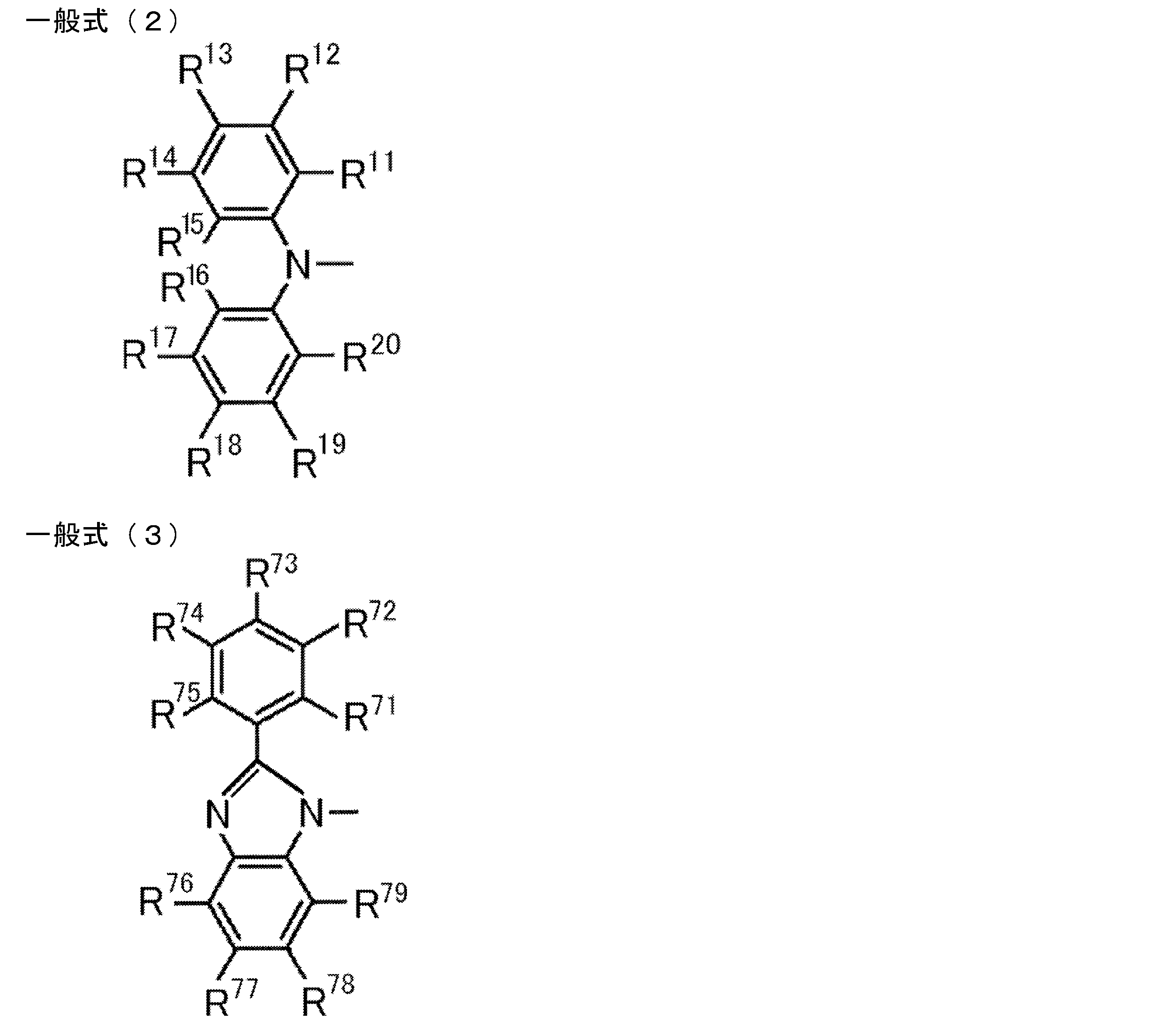
- R 11 to R 20 each independently represents a hydrogen atom or a substituent.
- R 11 and R 12 , R 12 and R 13 , R 13 and R 14 , R 14 and R 15 , R 15 and R 16 , R 16 and R 17 , R 17 and R 18 , R 18 and R 19 , R 19 And R 20 may be bonded to each other to form a cyclic structure.
- R 71 to R 79 each independently represents a hydrogen atom or a substituent.
- R 71 and R 72 , R 72 and R 73 , R 73 and R 74 , R 74 and R 75 , R 76 and R 77 , R 77 and R 78 , R 78 and R 79 are bonded to each other to form a cyclic structure You may do it.
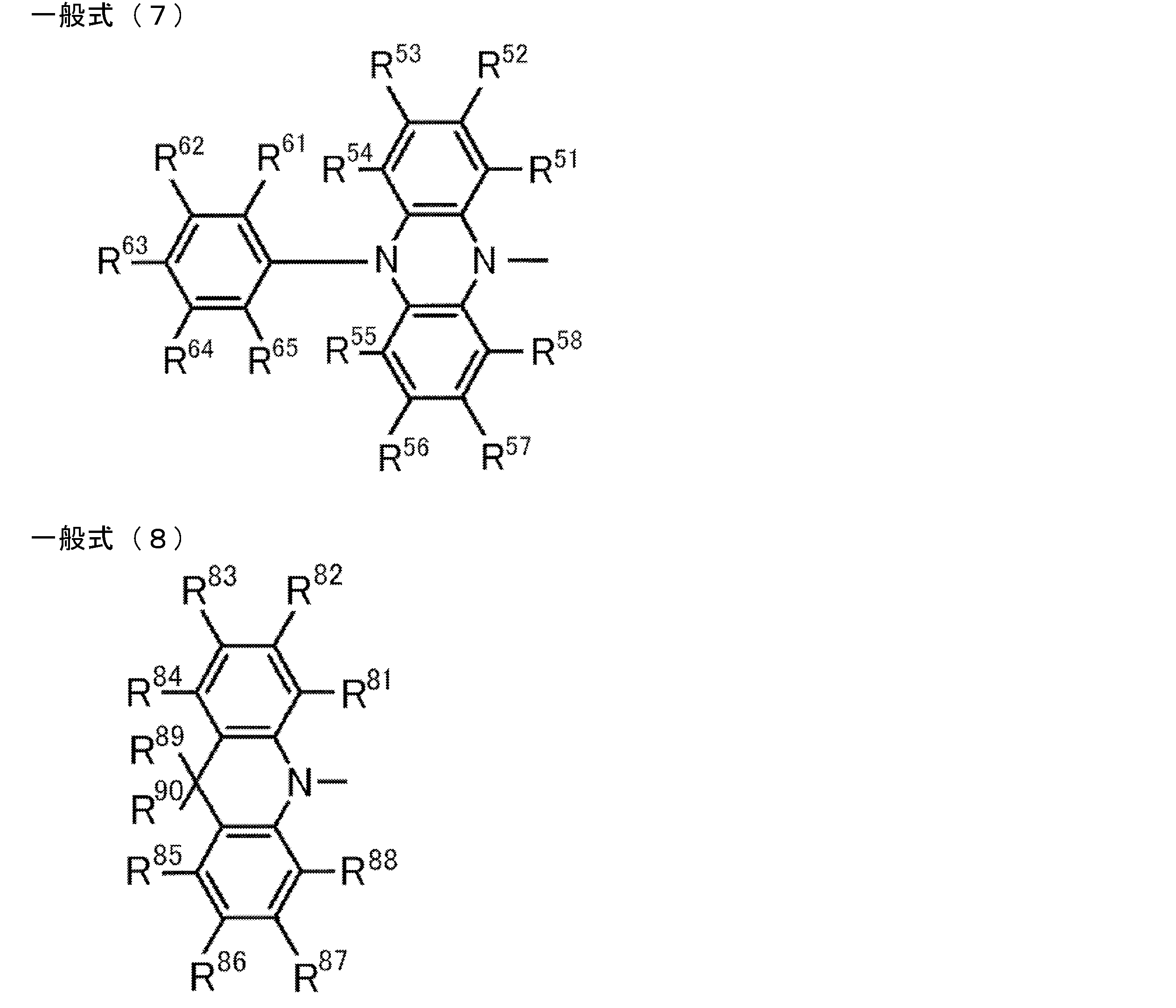
- [2] The compound according to [1], wherein the group represented by the general formula (2) is a group represented by any one of the following general formulas (4) to (8).
- R 21 to R 24 , R 27 to R 38 , R 41 to R 48 , R 51 to R 58 , R 61 to R 65 , R 81 to R 90 are Independently represents a hydrogen atom or a substituent.
- a mixture comprising a material composed of the compound represented by the general formula (1) and a light emitting material doped in the material.
- a light emitting layer comprising a material represented by the general formula (1) and a light emitting material doped in the material.
- the compound represented by the general formula (1) is an organic compound having the highest lowest excited singlet energy level among the organic compounds contained in the light emitting layer. Light emitting layer.
- the compound represented by the general formula (1), the difference Delta] E st in energy between the lowest excited triplet state of lowest excited singlet state and 77K are equal to or less than 0.3 eV
- the light emitting layer of description [13] The light emitting layer according to [9], further comprising a host.
- An assist dopant comprising a compound represented by the following general formula (1).
- R 1 to R 5 each independently represents a hydrogen atom or a substituent other than a cyano group, and at least one of R 1 to R 5 independently represents the following General Formula (2) or It is group represented by following General formula (3).
- R 11 to R 20 each independently represents a hydrogen atom or a substituent.
- R 11 and R 12 , R 12 and R 13 , R 13 and R 14 , R 14 and R 15 , R 15 and R 16 , R 16 and R 17 , R 17 and R 18 , R 18 and R 19 , R 19 And R 20 may be bonded to each other to form a cyclic structure.
- R 71 to R 79 each independently represents a hydrogen atom or a substituent.
- R 71 and R 72 , R 72 and R 73 , R 73 and R 74 , R 74 and R 75 , R 76 and R 77 , R 77 and R 78 , R 78 and R 79 are bonded to each other to form a cyclic structure You may do it.
- R 71 and R 72 , R 72 and R 73 , R 73 and R 74 , R 74 and R 75 , R 76 and R 77 , R 77 and R 78 , R 78 and R 79 are bonded to each other to form a cyclic structure You may do it.
- R 71 to R 79 each independently represents a hydrogen atom or a substituent.
- the compound of the present invention is useful as a host and assist dopant.
- An organic light emitting device using the compound of the present invention as a host or assist dopant can realize high luminous efficiency.
- 2 is an absorption emission spectrum of a toluene solution of Compound 1 of Test Example 1.
- 2 is a transient decay curve of a toluene solution of Compound 1 of Test Example 1.
- 2 is a transient decay curve of a thin film of Compound 1 of Test Example 1.
- 2 shows an immediate emission spectrum and a delayed emission spectrum of a thin film of Compound 1 of Test Example 1.
- 2 is an absorption emission spectrum of a toluene solution of Compound 2 of Test Example 2.
- 3 is a transient decay curve of a toluene solution of Compound 2 of Test Example 2.
- 3 is a transient decay curve of a thin film of Compound 2 of Test Example 2.
- 2 shows an immediate emission spectrum and a delayed emission spectrum of a thin film of Compound 2 of Test Example 2.
- 2 is an absorption emission spectrum of a toluene solution of Compound 3 of Test Example 3.
- 4 is a transient decay curve of a toluene solution of Compound 3 of Test Example 3.
- 4 is a transient decay curve of a thin film of Compound 3 of Test Example 3.
- 2 shows an immediate emission spectrum and a delayed emission spectrum of a thin film of Compound 3 of Test Example 3.
- 4 is an absorption emission spectrum of a toluene solution of Compound 4 of Test Example 4.
- 6 is a transient decay curve of a toluene solution of Compound 4 of Test Example 4.
- 6 is a transient decay curve of a thin film of Compound 4 of Test Example 4.
- 6 is an absorption emission spectrum of a toluene solution of Compound 5 of Test Example 5.
- 6 is a transient decay curve of a toluene solution of Compound 5 of Test Example 5.
- 2 is an absorption emission spectrum of a toluene solution of Compound 6 of Test Example 6.
- 7 is a transient decay curve of a toluene solution of Compound 6 of Test Example 6.
- 7 is a transient decay curve of a thin film of Compound 6 of Test Example 6.
- 2 shows an immediate emission spectrum and a delayed emission spectrum of a thin film of Compound 6 of Test Example 6.
- 2 is a transient decay curve of the organic electroluminescence device of the compound 2 of Example 1. It is the immediate fluorescence spectrum and delayed fluorescence spectrum of the organic electroluminescent element of the compound 2 of Example 1. It is the immediate fluorescence spectrum and delayed fluorescence spectrum of the thin film of the compound 2 of Example 1.
- a numerical range represented by using “to” means a range including numerical values described before and after “to” as a lower limit value and an upper limit value.
- the isotope species of the hydrogen atom present in the molecule of the compound used in the present invention is not particularly limited. For example, all the hydrogen atoms in the molecule may be 1 H, or a part or all of the hydrogen atoms are 2 H. (Deuterium D) may be used.
- the compound of the present invention is a compound represented by the following general formula (1).
- R 1 to R 5 each independently represents a hydrogen atom or a substituent other than a cyano group, and at least one of R 1 to R 5 is each independently the following general formula (2) or It is group represented by General formula (3).
- the group represented by the general formula (2) or (3) may be only one of R 1 to R 5 or 2 to 5, but one or two It is preferable that When the group represented by the general formula (2) or (3) is only one of R 1 to R 5 , R 2 or R 3 is represented by the general formula (2) or (3) It is preferably a group, and R 3 is preferably a group represented by the general formula (2) or (3).
- R 1 to R 5 are groups represented by the general formula (2) or (3), R 1 or R 2 and R 4 or R 5 are represented by the general formula (2) or (3 ), And R 1 and R 5 are more preferably groups represented by the general formula (2) or (3).
- R 1 , R 3 and R 5 are represented by the general formula (2) or (3). It is preferable that it is group represented.
- R 1 , R 2 , R 4 , R 5 are represented by the general formula (2) or ( The group represented by 3) is preferable.
- R 11 to R 20 and R 71 to R 79 each independently represent a hydrogen atom or a substituent.
- the number of substituents is not particularly limited, and all of R 11 to R 20 and R 71 to R 79 may be unsubstituted (that is, a hydrogen atom).
- the plurality of substituents may be the same or different from each other. May be.
- the substituent is preferably any one of R 72 to R 74 , R 77 and R 78 .
- R 11 to R 20 and R 71 to R 79 can take include, for example, a hydroxy group, a halogen atom, a cyano group, an alkyl group having 1 to 20 carbon atoms, an alkoxy group having 1 to 20 carbon atoms, and 1 to 20 alkylthio groups, alkyl substituted amino groups having 1 to 20 carbon atoms, acyl groups having 2 to 20 carbon atoms, aryl groups having 6 to 40 carbon atoms, heteroaryl groups having 3 to 40 carbon atoms, and 2 to 10 carbon atoms Alkenyl group, alkynyl group having 2 to 10 carbon atoms, alkoxycarbonyl group having 2 to 10 carbon atoms, alkylsulfonyl group having 1 to 10 carbon atoms, haloalkyl group having 1 to 10 carbon atoms, amide group, 2 to 10 carbon atoms Alkylamide group, trialkylsilyl group having 3 to 20 carbon atoms, trial
- substituents are a halogen atom, a cyano group, a substituted or unsubstituted alkyl group having 1 to 20 carbon atoms, an alkoxy group having 1 to 20 carbon atoms, a substituted or unsubstituted aryl group having 6 to 40 carbon atoms, carbon A substituted or unsubstituted heteroaryl group having 3 to 40 carbon atoms, and a dialkyl-substituted amino group having 1 to 20 carbon atoms.
- substituents are a halogen atom, a cyano group, a substituted or unsubstituted alkyl group having 1 to 20 carbon atoms, an alkoxy group having 1 to 20 carbon atoms, a substituted or unsubstituted aryl group having 6 to 40 carbon atoms, carbon A substituted or unsubstituted heteroaryl group having 3 to 40 carbon atoms, and a dialkyl-substituted amino group having 1 to 20 carbon
- substituents are a fluorine atom, a chlorine atom, a cyano group, a substituted or unsubstituted alkyl group having 1 to 10 carbon atoms, a substituted or unsubstituted alkoxy group having 1 to 10 carbon atoms, and a substituted group having 6 to 15 carbon atoms.
- it is an unsubstituted aryl group or a substituted or unsubstituted heteroaryl group having 3 to 12 carbon atoms.
- An annular structure may be formed.
- the cyclic structure may be an aromatic ring or an alicyclic ring, may contain a hetero atom, and the cyclic structure may be a condensed ring of two or more rings.
- the hetero atom here is preferably selected from the group consisting of a nitrogen atom, an oxygen atom and a sulfur atom.
- cyclic structures formed include benzene ring, naphthalene ring, pyridine ring, pyridazine ring, pyrimidine ring, pyrazine ring, pyrrole ring, imidazole ring, pyrazole ring, triazole ring, imidazoline ring, oxazole ring, isoxazole ring, thiazole And a ring, an isothiazole ring, a cyclohexadiene ring, a cyclohexene ring, a cyclopentaene ring, a cycloheptatriene ring, a cycloheptadiene ring, and a cycloheptaene ring.
- the group represented by the general formula (2) is preferably a group represented by any one of the following general formulas (4) to (8), and is preferably a group represented by the general formula (8). More preferred.
- R 21 to R 24 , R 27 to R 38 , R 41 to R 48 , R 51 to R 58 , R 61 to R 65 , and R 81 to R 90 are each independent.
- the explanation and preferred ranges of the substituents that can be taken by the above R 11 to R 20 can be referred to.
- the number of substituents in the general formulas (4) to (8) is not particularly limited.
- R 21 to R 24 , R 27 to R 38 , R 41 to R 48 , R 51 to R 58 , R 61 to R 65 , R 81 to R 90 and the above R 71 to R 79 are each independently A group represented by any one of formulas (3) to (8) is also preferred. It is also preferred that all are unsubstituted (ie hydrogen atoms). Further, when each of the general formulas (4) to (8) has two or more substituents, these substituents may be the same or different. Further, when a substituent is present in the general formulas (4) to (8), the substituent is any one of R 22 to R 24 and R 27 to R 29 in the case of the general formula (4).
- R 23 and R 28 is preferably at least one of R 23 and R 28. If it is general formula (5), it is preferably any one of R 32 to R 37 , and if it is general formula (6), R 42 to R 47 are preferred, and in the case of the general formula (7), any of R 52 , R 53 , R 56 , R 57 , R 62 to R 64 is preferred. preferably if 8) R 82 is either ⁇ R 87, R 89, R 90, is preferably R 89 and R 90.
- the substituent represented by R 89 and R 90 is preferably a substituted or unsubstituted aryl group having 6 to 40 carbon atoms, and more preferably a substituted or unsubstituted phenyl group. Moreover, it is preferable that the substituent which R89 and R90 represent is the same.
- All the groups represented by the general formula (2) present in the general formula (1) are preferably groups represented by any one of the general formulas (4) to (8).
- the group which all is represented by General formula (8) can be illustrated preferably.
- R 1 to R 5 other than the group represented by the general formula (2) or (3) are each independently a hydrogen atom or a substituent other than a cyano group.
- the number of substituents taken by R 1 to R 5 other than the group represented by the general formula (2) or (3) is not particularly limited, and all the groups other than the group represented by the general formula (2) or (3) are used. It may be unsubstituted (that is, a hydrogen atom).
- the plurality of substituents may be the same as or different from each other.
- R 1 to R 5 For the description and preferred ranges of the substituents that R 1 to R 5 can take, reference can be made to the explanations and preferred ranges of the substituents that can be taken by the above R 11 to R 20 excluding the cyano group.
- R 3 is a group represented by the general formula (2) or a group represented by (3)
- at least one of R 1 , R 2 , R 4 , and R 5 has 1 to 20 carbon atoms.
- all of R 1 , R 2 , R 4 , and R 5 are more preferably alkyl groups having 1 to 20 carbon atoms.
- the alkyl group preferably has 1 to 10 carbon atoms, more preferably 1 to 6 carbon atoms, and still more preferably 1 to 3 carbon atoms.
- the molecular weight of the compound represented by the general formula (1) is, for example, 1500 or less when the organic layer containing the compound represented by the general formula (1) is intended to be formed by vapor deposition. Preferably, it is preferably 1200 or less, more preferably 1000 or less, and even more preferably 800 or less.
- the lower limit of the molecular weight is the molecular weight of the minimum compound represented by the general formula (1).
- the compound represented by the general formula (1) may be formed by a coating method regardless of the molecular weight. If a coating method is used, a film can be formed even with a compound having a relatively large molecular weight.
- the compound represented by the general formula (1) is useful as a host and assist dopant in the light emitting layer.
- a compound containing a plurality of structures represented by the general formula (1) in the molecule may be used as a host or assist dopant.
- a polymer obtained by previously polymerizing a polymerizable group in the structure represented by the general formula (1) and polymerizing the polymerizable group as a host and an assist dopant.
- a monomer containing a polymerizable functional group in any of R 1 to R 5 of the general formula (1) and polymerizing it alone or copolymerizing with other monomers, It is conceivable to obtain a polymer having a repeating unit and use the polymer as a host and an assist dopant.
- dimers and trimers are obtained by reacting compounds having a structure represented by the general formula (1) and used as a host and assist dopant.
- the polymer having a repeating unit containing a structure represented by the general formula (1) include a polymer containing a structure represented by the following general formula (9) or (10).
- Q represents a group including the structure represented by General Formula (1)
- L 1 and L 2 represent a linking group.
- the linking group preferably has 0 to 20 carbon atoms, more preferably 1 to 15 carbon atoms, and still more preferably 2 to 10 carbon atoms. And preferably has a structure represented by - linking group -X 11 -L 11.
- X 11 represents an oxygen atom or a sulfur atom, and is preferably an oxygen atom.
- L 11 represents a linking group, and is preferably a substituted or unsubstituted alkylene group, or a substituted or unsubstituted arylene group, and is a substituted or unsubstituted alkylene group having 1 to 10 carbon atoms, or a substituted or unsubstituted group A phenylene group is more preferable.
- R 101 , R 102 , R 103 and R 104 each independently represent a substituent.
- it is a substituted or unsubstituted alkyl group having 1 to 6 carbon atoms, a substituted or unsubstituted alkoxy group having 1 to 6 carbon atoms, or a halogen atom, more preferably an unsubstituted alkyl group having 1 to 3 carbon atoms.
- An unsubstituted alkoxy group having 1 to 3 carbon atoms, a fluorine atom, and a chlorine atom and more preferably an unsubstituted alkyl group having 1 to 3 carbon atoms and an unsubstituted alkoxy group having 1 to 3 carbon atoms.
- the linking group represented by L 1 and L 2 is any one of R 1 to R 5 in the structure of the general formula (1) constituting Q, any of R 11 to R 20 in the general formula (2), Any of R 71 to R 78 having the structure of the formula (3), any of R 21 to R 24 and R 27 to R 30 having the structure of the general formula (4), and R 31 to having the structure of the general formula (5) Any of R 38 , any of R 41 to R 48 having the structure of the general formula (6), any of R 51 to R 58 and R 61 to R 65 having the structure of the general formula (7), ) To any one of R 81 to R 90 of the structure.
- Two or more linking groups may be linked to one Q to form a crosslinked structure or a network structure.
- repeating unit examples include structures represented by the following formulas (11) to (14).
- a hydroxy group is introduced into any one of R 1 to R 5 in the structure of the general formula (1), and this is used as a linker as described below. It can be synthesized by reacting a compound to introduce a polymerizable group and polymerizing the polymerizable group.
- the polymer containing the structure represented by the general formula (1) in the molecule may be a polymer composed only of repeating units having the structure represented by the general formula (1), or other structures may be used. It may be a polymer containing repeating units.
- the repeating unit having a structure represented by the general formula (1) contained in the polymer may be a single type or two or more types. Examples of the repeating unit not having the structure represented by the general formula (1) include those derived from monomers used in ordinary copolymerization. Examples thereof include a repeating unit derived from a monomer having an ethylenically unsaturated bond such as ethylene and styrene.
- the compound represented by the general formula (1) can be synthesized by combining known reactions.
- a compound in which R 3 in the general formula (1) is a group represented by the general formula (2) can be synthesized by reacting the following two compounds.
- R 1 , R 2 , R 4 , R 5 , R 11 to R 20 in the above reaction formula the corresponding description in general formula (1) can be referred to.
- X represents a halogen atom, and examples thereof include a fluorine atom, a chlorine atom, a bromine atom, and an iodine atom, and a chlorine atom, a bromine atom, and an iodine atom are preferable.
- the above reaction is an application of a known coupling reaction, and known reaction conditions can be appropriately selected and used. The details of the above reaction can be referred to the synthesis examples described below.
- the compound represented by the general formula (1) can also be synthesized by combining other known synthesis reactions.
- the compound represented by the general formula (1) of the present invention can constitute a mixture in which a material made of the compound is doped with a light emitting material. Such a mixture can be suitably used as a material for a light emitting layer of an organic light emitting device, for example. In the mixture, one type of the compound represented by the general formula (1) may be used alone, or two or more types may be used in combination.
- the light emitting material may be any of a red light emitting material, a green light emitting material, and a blue light emitting material, and may be a mixture of two or three color light emitting materials.
- each of the red light emitting material, the green light emitting material, and the blue light emitting material may be composed of one kind of organic compound, or may be a combination of two or more kinds of organic compounds.
- the content of the compound represented by the general formula (1) in the mixture is larger than the content of the light emitting material.
- the mixture may contain an organic compound other than the compound represented by the general formula (1) and the light emitting material. Specific examples of the light emitting material, specific examples of the organic compound that can be used other than the compound represented by the general formula (1) and the light emitting material, specific examples of the light emitting material and other organic compounds used in the following light emitting layer Can be referred to.
- the compound represented by the general formula (1) of the present invention is useful as a host and assist dopant in an organic light-emitting device. Therefore, the compound represented by the general formula (1) of the present invention can be effectively used as a host or assist dopant in the light emitting layer of the organic light emitting device, thereby realizing an organic light emitting device with high light emission efficiency. be able to.
- the “host” is an organic compound contained in the light emitting layer together with the light emitting material, and is an organic compound having the highest lowest excited singlet energy level among the organic compounds contained in the light emitting layer.
- the “assist dopant” means that the light emitting material including at least the assist dopant, the host, and the light emitting material has higher luminous efficiency than the light emitting layer having the same composition except that the assist dopant is not included.
- An organic compound An organic compound.
- an organic light-emitting device organic light-emitting device of the present invention containing a compound represented by the general formula (1) and a light-emitting material in a light-emitting layer will be specifically described.
- the organic light-emitting device of the present invention may be an organic photoluminescence device (organic PL device) or an organic electroluminescence device (organic EL device).
- the organic photoluminescence element has a structure in which at least a light emitting layer is formed on a substrate.
- the organic electroluminescence element has a structure in which an organic layer is formed at least between an anode, a cathode, and an anode and a cathode.
- the organic layer includes at least a light emitting layer, and may consist of only the light emitting layer, or may have one or more organic layers in addition to the light emitting layer.
- Examples of such other organic layers include a hole transport layer, a hole injection layer, an electron blocking layer, a hole blocking layer, an electron injection layer, an electron transport layer, and an exciton blocking layer.
- the hole transport layer may be a hole injection / transport layer having a hole injection function
- the electron transport layer may be an electron injection / transport layer having an electron injection function.
- FIG. 1 A specific example of the structure of an organic electroluminescence element is shown in FIG. In FIG. 1, 1 is a substrate, 2 is an anode, 3 is a hole injection layer, 4 is a hole transport layer, 5 is a light emitting layer, 6 is an electron transport layer, and 7 is a cathode. Below, each member and each layer of an organic electroluminescent element are demonstrated. In addition, description of a board
- the light emitting layer is a layer that emits light after excitons are generated by recombination of holes and electrons injected from the anode and the cathode, respectively.
- the light emitting layer contains the compound represented by the general formula (1) and a light emitting material.
- the compound represented by the general formula (1) may be used as a host or an assist dopant. (System using a compound represented by the general formula (1) as a host)
- the light emitting layer using the compound represented by the general formula (1) as a host is formed by doping a host composed of the compound represented by the general formula (1) with a light emitting material, and represented by the general formula (1).
- the compound to be formed is configured such that the lowest excited singlet energy level is the highest among the organic compounds constituting the light emitting layer.
- the excited singlet energy generated by the compound represented by the general formula (1) by recombination of holes and electrons easily moves to the light emitting material and is confined in the light emitting material. It is estimated that it contributes effectively. As a result, high luminous efficiency can be obtained.
- the compound represented by the general formula (1) used as a host is preferably a delayed phosphor.
- the term “delayed phosphor” refers to a state in which, after transitioning to the excited triplet state, the excited singlet state can cross between the reverse terms, and the excited singlet state returns to the ground state.
- An organic compound that emits fluorescence Note that the lifetime of light generated by reverse intersystem crossing from the excited triplet state to the excited singlet state is longer than normal fluorescence (immediate fluorescence) or phosphorescence, and thus is observed as fluorescence delayed from these.
- the compound represented by the general formula (1) is a delayed phosphor
- high luminous efficiency is obtained for the following reason. That is, when holes and electrons recombine on the host molecules in the light-emitting layer, the host is excited from the ground state to the excited singlet state and excited triplet state, but when the host is a delayed phosphor, the excited triplet A host molecule excited to a state transitions to an excited singlet state through reverse intersystem crossing. For this reason, in addition to the excited singlet energy directly generated by recombination of holes and electrons, the excited triplet energy can also be used as excited singlet energy through reverse intersystem crossing. Since both excited singlet energies move to the light emitting material to cause the light emitting material to emit light, it is estimated that high light emission efficiency can be obtained.
- the content of the compound represented by the general formula (1) and the light emitting material contained in the light emitting layer is not particularly limited, but the content of the compound represented by the general formula (1) as a host is more than the content of the light emitting material. Is also preferably large. Specifically, when the total mass of the content of the compound represented by the general formula (1) and the content of the light emitting material is 100% by mass, the content of the compound represented by the general formula (1) is: The content is preferably 50% by mass or more and 99.9% by mass or less, and the content of the light emitting material is more preferably 0.1% by mass or more and 50% by mass or less.
- the light emitting layer using the compound represented by the general formula (1) as an assist dopant is configured by doping a host with an assist dopant made of the compound represented by the general formula (1) and a light emitting material.
- the host is an organic compound other than the compound represented by the general formula (1) and the light emitting material, and is the organic compound having the highest lowest excited singlet energy level among the organic compounds contained in the light emitting layer. .
- the compound represented by the general formula (1) is a delayed phosphor, and the host material and the compound represented by the general formula (1) It is preferable that the light emitting material satisfies the following formula (A).
- E S1 (A)> E S1 (B)> E S1 (C) In the above formula, E S1 (A) represents the lowest excited singlet energy level of the host, and E S1 (B) represents the lowest excited singlet energy level of the compound represented by the general formula (1) which is an assist dopant. E S1 (C) represents the lowest excited singlet energy level of the luminescent material.
- the compound represented by General formula (1) can be effectively functioned as an assist dopant, and luminous efficiency can be further increased. This is presumably due to the following reasons. That is, when excitation energy is generated by recombination of holes and electrons in the light emitting layer, each compound contained in the light emitting layer is excited from the ground state to the excited singlet state and the excited triplet state. At this time, when the compound represented by the general formula (1) which is the host and the assist dopant and the light emitting material satisfy the formula (A), the excited singlet of the compound represented by the host and the general formula (1). The energy easily moves to the light emitting material, and the light emitting material in the ground state transitions to the excited singlet state.
- the light emitting material that has been in an excited singlet state emits fluorescence (radiation deactivation) when it subsequently returns to the ground state.
- a molecule excited to an excited triplet state transitions to an excited singlet state through reverse intersystem crossing.
- the excited triplet energy can also be used as excited singlet energy through reverse intersystem crossing. Since both of these excited singlet energies and the excited singlet energy generated by the host move to the light emitting material and contribute to light emission of the light emitting material, it is presumed that higher luminous efficiency can be obtained.
- E T1 (A) represents the lowest excited triplet energy level of the host at 77K
- E T1 (B) represents the lowest excited triplet of the compound represented by the general formula (1) as an assist dopant at 77K. It represents the term energy level.
- the relationship between the lowest excited triplet energy level E T1 (B) at 77K of the compound represented by the general formula (1) and the lowest excited triplet energy level E T1 (C) at 77K of the light emitting material is not particularly limited. May be selected so that, for example, E T1 (B)> E T1 (C).
- E T1 (B)> E T1 (C) When the host and the compound represented by the general formula (1) satisfy the formula (B), the excited triplet energy generated by the host easily moves to the compound represented by the general formula (1), The compound is excited to the excited triplet state.
- the molecule excited to the excited triplet state transitions to the excited singlet state through the intersystem crossing, and as a result
- the excited triplet energy generated by the host is also presumed to contribute effectively to the light emission of the light emitting material as excited singlet energy. Thereby, higher luminous efficiency can be obtained.
- the content of the host, the compound represented by the general formula (1) and the light emitting material are not particularly limited, but the content of the compound represented by the general formula (1) is more than the content of the host. Small is preferable. Thereby, higher luminous efficiency can be obtained.
- the content W1 of the host is 15
- the content W2 of the compound represented by the general formula (1) is preferably 5.0% by weight or more and 50% by weight or less, preferably the light emitting material.
- the content W3 of is preferably 0.5% by weight or more and 5.0% by weight or less.
- the compound represented by the general formula (1) is a delayed phosphor in both cases where it is used as a host and when it is used as an assist dopant.
- This delayed phosphor is preferably a thermally activated delayed phosphor that reversely crosses from the excited singlet state to the excited triplet state by absorption of thermal energy.
- Thermally activated delayed phosphor absorbs the heat generated by the device and crosses the reverse triplet from the excited triplet state to the excited singlet relatively easily and efficiently contributes to the emission of the excited triplet energy. Can do.
- the difference ⁇ E st between the energy level E s1 in the lowest excited singlet state and the energy level E T1 in the lowest excited triplet state of 77K is 0. 0.3 eV or less is preferable, 0.2 eV or less is more preferable, 0.1 eV or less is further preferable, and 0.08 eV or less is even more preferable.
- the delayed phosphor having the energy difference ⁇ E st in the above range the back-to-back crossing from the excited triplet state to the excited singlet state occurs relatively easily, and the excited triplet energy can efficiently contribute to light emission. .
- the light emitting material used in the system using the compound represented by the general formula (1) as a host and the system using the compound represented by the general formula (1) as an assist dopant a known light emitting material can be used, and at least A luminescent material that can emit fluorescence is preferable, and delayed fluorescence or phosphorescence may be emitted together with fluorescence.
- the following compounds can be preferably used.
- the host used in the system using the compound represented by the general formula (1) as assist dopan is not particularly limited except that the lowest excited singlet energy level is the highest among the organic compounds contained in the light emitting layer.
- a host generally used in the light emitting layer can be used.
- an organic compound that has a hole transporting ability and an electron transporting ability, prevents emission of longer wavelengths, and has a high glass transition temperature is preferable.
- light emission mainly occurs from the light emitting material, but it may be a part or part of the light emission from the compound or host represented by the general formula (1). Further, this light emission is at least fluorescent light emission, and may include delayed fluorescent light emission or phosphorescent light emission.
- the light emitting layer may be composed of only the compound represented by the general formula (1) and a light emitting material, or may contain other organic compounds. May be.
- the light emitting layer may be composed only of the compound represented by the general formula (1), a light emitting material, and a host.
- An organic compound may be included. Examples of other organic compounds include organic compounds having a hole transport ability, organic compounds having an electron transport ability, and the like. As the organic compound having a hole transport ability and the organic compound having an electron transport ability, the following hole transport material and electron transport material can be referred to.
- the organic electroluminescence device of the present invention is preferably supported on a substrate.
- the substrate is not particularly limited and may be any substrate conventionally used for organic electroluminescence elements.
- a substrate made of glass, transparent plastic, quartz, silicon, or the like can be used.
- an electrode material made of a metal, an alloy, an electrically conductive compound, or a mixture thereof having a high work function (4 eV or more) is preferably used.
- electrode materials include metals such as Au, and conductive transparent materials such as CuI, indium tin oxide (ITO), SnO 2 and ZnO.
- conductive transparent materials such as CuI, indium tin oxide (ITO), SnO 2 and ZnO.
- an amorphous material such as IDIXO (In 2 O 3 —ZnO) capable of forming a transparent conductive film may be used.
- a thin film may be formed by vapor deposition or sputtering of these electrode materials, and a pattern of a desired shape may be formed by photolithography, or when pattern accuracy is not so high (about 100 ⁇ m or more) ), A pattern may be formed through a mask having a desired shape at the time of vapor deposition or sputtering of the electrode material.
- wet film-forming methods such as a printing system and a coating system, can also be used.
- the transmittance be greater than 10%, and the sheet resistance as the anode is preferably several hundred ⁇ / ⁇ or less.
- the film thickness depends on the material, it is usually selected in the range of 10 to 1000 nm, preferably 10 to 200 nm.
- cathode a material having a low work function (4 eV or less) metal (referred to as an electron injecting metal), an alloy, an electrically conductive compound, and a mixture thereof as an electrode material is used.
- electrode materials include sodium, sodium-potassium alloy, magnesium, lithium, magnesium / copper mixture, magnesium / silver mixture, magnesium / aluminum mixture, magnesium / indium mixture, aluminum / aluminum oxide (Al 2 O 3 ) Mixtures, indium, lithium / aluminum mixtures, rare earth metals and the like.
- a mixture of an electron injecting metal and a second metal which is a stable metal having a larger work function value than this for example, a magnesium / silver mixture, Magnesium / aluminum mixtures, magnesium / indium mixtures, aluminum / aluminum oxide (Al 2 O 3 ) mixtures, lithium / aluminum mixtures, aluminum and the like are preferred.
- the cathode can be produced by forming a thin film of these electrode materials by a method such as vapor deposition or sputtering.
- the sheet resistance as the cathode is preferably several hundred ⁇ / ⁇ or less, and the film thickness is usually selected in the range of 10 nm to 5 ⁇ m, preferably 50 to 200 nm.
- the emission luminance is advantageously improved.
- a transparent or semi-transparent cathode can be produced. By applying this, an element in which both the anode and the cathode are transparent is used. Can be produced.
- the injection layer is a layer provided between the electrode and the organic layer for lowering the driving voltage and improving the luminance of light emission.
- the injection layer can be provided as necessary.
- the blocking layer is a layer that can prevent diffusion of charges (electrons or holes) and / or excitons existing in the light emitting layer to the outside of the light emitting layer.
- the electron blocking layer can be disposed between the light emitting layer and the hole transport layer and blocks electrons from passing through the light emitting layer toward the hole transport layer.
- a hole blocking layer can be disposed between the light emitting layer and the electron transporting layer to prevent holes from passing through the light emitting layer toward the electron transporting layer.
- the blocking layer can also be used to block excitons from diffusing outside the light emitting layer. That is, each of the electron blocking layer and the hole blocking layer can also function as an exciton blocking layer.
- the term “electron blocking layer” or “exciton blocking layer” as used herein is used in the sense of including a layer having the functions of an electron blocking layer and an exciton blocking layer in one layer.
- the hole blocking layer has a function of an electron transport layer in a broad sense.
- the hole blocking layer has a role of blocking holes from reaching the electron transport layer while transporting electrons, thereby improving the recombination probability of electrons and holes in the light emitting layer.
- the material for the hole blocking layer the material for the electron transport layer described later can be used as necessary.
- the electron blocking layer has a function of transporting holes in a broad sense.
- the electron blocking layer has a role to block electrons from reaching the hole transport layer while transporting holes, thereby improving the probability of recombination of electrons and holes in the light emitting layer. .
- the exciton blocking layer is a layer for preventing excitons generated by recombination of holes and electrons in the light emitting layer from diffusing into the charge transport layer. It becomes possible to efficiently confine in the light emitting layer, and the light emission efficiency of the device can be improved.
- the exciton blocking layer can be inserted on either the anode side or the cathode side adjacent to the light emitting layer, or both can be inserted simultaneously.
- the layer when the exciton blocking layer is provided on the anode side, the layer can be inserted adjacent to the light emitting layer between the hole transport layer and the light emitting layer, and when inserted on the cathode side, the light emitting layer and the cathode Between the luminescent layer and the light-emitting layer.
- a hole injection layer, an electron blocking layer, or the like can be provided between the anode and the exciton blocking layer adjacent to the anode side of the light emitting layer, and the excitation adjacent to the cathode and the cathode side of the light emitting layer can be provided.
- an electron injection layer, an electron transport layer, a hole blocking layer, and the like can be provided.
- the blocking layer is disposed, at least one of the excited singlet energy and the excited triplet energy of the material used as the blocking layer is preferably higher than the excited singlet energy and the excited triplet energy of the light emitting material.
- the hole transport layer is made of a hole transport material having a function of transporting holes, and the hole transport layer can be provided as a single layer or a plurality of layers.
- the hole transport material has any one of hole injection or transport and electron barrier properties, and may be either organic or inorganic.
- hole transport materials that can be used include, for example, triazole derivatives, oxadiazole derivatives, imidazole derivatives, carbazole derivatives, indolocarbazole derivatives, polyarylalkane derivatives, pyrazoline derivatives and pyrazolone derivatives, phenylenediamine derivatives, arylamine derivatives, Examples include amino-substituted chalcone derivatives, oxazole derivatives, styrylanthracene derivatives, fluorenone derivatives, hydrazone derivatives, stilbene derivatives, silazane derivatives, aniline copolymers, and conductive polymer oligomers, particularly thiophene oligomers.
- An aromatic tertiary amine compound and an styrylamine compound are preferably used, and an aromatic tertiary amine compound is more preferably used.
- the electron transport layer is made of a material having a function of transporting electrons, and the electron transport layer can be provided as a single layer or a plurality of layers.
- the electron transport material (which may also serve as a hole blocking material) may have a function of transmitting electrons injected from the cathode to the light emitting layer.
- Examples of the electron transport layer that can be used include nitro-substituted fluorene derivatives, diphenylquinone derivatives, thiopyran dioxide oxide derivatives, carbodiimides, fluorenylidenemethane derivatives, anthraquinodimethane and anthrone derivatives, oxadiazole derivatives, and the like.
- a thiadiazole derivative in which the oxygen atom of the oxadiazole ring is substituted with a sulfur atom, and a quinoxaline derivative having a quinoxaline ring known as an electron withdrawing group can also be used as an electron transport material.
- a polymer material in which these materials are introduced into a polymer chain or these materials are used as a polymer main chain can also be used.
- the compound represented by the general formula (1) may be used not only for the light emitting layer but also for layers other than the light emitting layer.
- the compound represented by General formula (1) used for a light emitting layer and the compound represented by General formula (1) used for layers other than a light emitting layer may be same or different.
- the compound represented by the general formula (1) may be used for the injection layer, blocking layer, hole blocking layer, electron blocking layer, exciton blocking layer, hole transporting layer, electron transporting layer, and the like. .
- the method for forming these layers is not particularly limited, and the layer may be formed by either a dry process or a wet process.
- the preferable material which can be used for an organic electroluminescent element is illustrated concretely.
- the material that can be used in the present invention is not limited to the following exemplary compounds.
- R and R 2 to R 7 in the structural formulas of the following exemplary compounds each independently represent a hydrogen atom or a substituent.
- n represents an integer of 3 to 5.
- the organic electroluminescence device produced by the above-described method emits light by applying an electric field between the anode and the cathode of the obtained device. At this time, if the light is emitted by excited singlet energy, light having a wavelength corresponding to the energy level is confirmed as fluorescence emission and delayed fluorescence emission. Further, in the case of light emission by excited triplet energy, a wavelength corresponding to the energy level is confirmed as phosphorescence. Since normal fluorescence has a shorter fluorescence lifetime than delayed fluorescence, the emission lifetime can be distinguished from fluorescence and delayed fluorescence.
- the excited triplet energy is unstable and is converted into heat or the like, and the lifetime is short and it is immediately deactivated.
- the excited triplet energy of a normal organic compound it can be measured by observing light emission under extremely low temperature conditions.
- the organic electroluminescence element of the present invention can be applied to any of a single element, an element having a structure arranged in an array, and a structure in which an anode and a cathode are arranged in an XY matrix.
- an organic light emitting device having greatly improved light emission efficiency can be obtained by incorporating the compound represented by the general formula (1) into the light emitting layer as a host or assist dopant.
- the organic light emitting device such as the organic electroluminescence device of the present invention can be further applied to various uses. For example, it is possible to produce an organic electroluminescence display device using the organic electroluminescence element of the present invention.
- organic electroluminescence device of the present invention can be applied to organic electroluminescence illumination and backlights that are in great demand.
- Photonics C11347), source meter (Ceethley: 2400 series), semiconductor parameter analyzer (Agilent Technology: E5273A), optical power meter measuring device (Newport: 1930C), optical spectrometer ( The measurement was carried out using a spectroradiometer (manufactured by Topcon Co., Ltd .: SR-3) and a streak camera (C4334, manufactured by Hamamatsu Photonics Co., Ltd.).
- the lowest excited singlet energy level E S1 and the lowest excited triplet energy level E T1 of the compounds used in Examples and Comparative Examples were determined by the following procedure.
- the energy difference ⁇ E st between the lowest excited singlet state and the lowest excited triplet state of 77K was obtained by calculating the difference between E S1 and E T1 .
- (1) Lowest excited singlet energy level E S1 The sample to be measured was deposited on a Si substrate to prepare a sample, and the fluorescence spectrum of this sample was measured at room temperature (300K). In the fluorescence spectrum, the vertical axis represents light emission and the horizontal axis represents wavelength.
- the maximum point having a peak intensity of 10% or less of the maximum peak intensity of the spectrum is not included in the above-mentioned maximum value on the shortest wavelength side, and has the maximum slope value closest to the maximum value on the shortest wavelength side.
- the tangent drawn at the point where the value was taken was taken as the tangent to the rising edge of the phosphorescence spectrum on the short wavelength side.
- Synthesis Example 1 Synthesis of Compound 1 4-bromobenzonitrile (0.5 g, 2.75 mmol), 9,9-diphenylacridine (0.99 g, 3.0 mmol), tris (dibenzylideneacetone) dipalladium (0.76 g, 0.825 mmol), tri -Tert-butylphosphonium tetrafluoroborate (0.96 g, 3.3 mmol) and sodium tert-butoxide (0.53 g, 5.5 mmol) were added to a 100 ml container, and nitrogen substitution was performed three times. Thereafter, 30 ml of toluene was added, and the mixture was heated and stirred at 110 ° C. for 24 hours.
- the reaction mixture was cooled to room temperature, diluted with toluene, filtered through celite, and concentrated.
- the yield was 0.987 g, and the yield was 83%.
- Synthesis Example 2 Synthesis of Compound 2 The same procedure as in Synthesis Example 1 was conducted except that 4-bromobenzonitrile was changed to 3-bromobenzonitrile (0.5 g, 2.75 mmol), whereby 3- (10H-9, 9-Diphenylacridin-10-yl) benzonitrile was obtained in a yield of 0.861 g and a yield of 72%.
- Synthesis Example 3 Synthesis of Compound 3 The same procedure as in Synthesis Example 1 was carried out except that 4-bromobenzonitrile was changed to 2-bromobenzonitrile (0.5 g, 2.75 mmol), whereby 2- (10H-9, 9-Diphenylacridin-10-yl) benzonitrile was obtained in a yield of 1.022 g and a yield of 86%.
- Table 1 shows the characteristic values of the compounds 1 to 6 synthesized as described above. Note that HOMO is a value determined by measurement by atmospheric photoelectron spectroscopy, and LUMO is a value determined by using the energy gap obtained by the absorption spectrum edge.
- Test Example 1 Preparation and Evaluation of Compound 1 Solution and Thin Film
- a toluene solution of Compound 1 (concentration 10 ⁇ 4 to 10 ⁇ 5 mol / L) was prepared in a glove box under an Ar atmosphere. Further, a thin film of Compound 1 having a thickness of 100 nm was formed on a quartz substrate by a vacuum deposition method at a degree of vacuum of 5 ⁇ 10 ⁇ 4 Pa or less.
- FIG. 2 shows the result of measuring the absorption emission spectrum of the toluene solution of Compound 1 with 353 nm excitation light. The photoluminescence quantum efficiency was 24% for the toluene solution before bubbling with nitrogen and 29% for the toluene solution bubbled with nitrogen.
- FIG. 4 shows a transient attenuation curve of the thin film of Compound 1 measured at 300K and 5K with 337 nm excitation light. From FIG. 4, it was confirmed that the delayed fluorescence component was a thermally activated delayed fluorescence with an increase in temperature. Moreover, the photoluminescence quantum efficiency of the thin film of Compound 1 was 12.2%.
- FIG. 5 shows the immediate emission spectrum (Prompt) and delayed emission spectrum (Delay) of the thin film of Compound 1 measured at each temperature of 300K and 5K.
- a fast component is an immediate emission spectrum (Prompt)
- a slow component is a delayed emission spectrum (Delay).
- the immediate emission spectrum at 300K corresponds to the fluorescence spectrum
- the delayed emission spectrum at 300K corresponds to the delayed fluorescence spectrum.
- the immediate emission spectrum at 5K corresponds to the fluorescence spectrum
- the delayed emission spectrum corresponds to the phosphorescence spectrum.
- FIG. 6 shows the result of measuring the absorption emission spectrum of the toluene solution of Compound 2 with excitation light at 340 nm.
- the photoluminescence quantum efficiency was 4% with the toluene solution before bubbling with nitrogen, and 10% with the toluene solution bubbled with nitrogen.
- the result of measuring the transient decay curve for the toluene solution of Compound 2 is shown in FIG. In addition, FIG.
- FIG. 8 shows a transient decay curve by 337 nm excitation light measured at 300K, 200K, 100K, and 5K for the thin film of Compound 2. From FIG. 8, it was confirmed that the delayed fluorescence component is a thermally activated delayed fluorescence that increases with increasing temperature. Further, the photoluminescence quantum efficiency of the thin film of Compound 2 was 9.8%.
- FIG. 9 shows the immediate emission spectrum (Prompt) and delayed emission spectrum (Delay) of the thin film of Compound 2 measured at temperatures of 300K and 5K.
- the immediate emission spectrum at 300K corresponds to the fluorescence spectrum
- the delayed emission spectrum at 300K corresponds to the delayed fluorescence spectrum.
- the immediate emission spectrum at 5K corresponds to the fluorescence spectrum
- the delayed emission spectrum corresponds to the phosphorescence spectrum.
- FIG. 10 shows the result of measuring the absorption emission spectrum of the compound 3 in toluene solution using 340 nm excitation light. The photoluminescence quantum efficiency was 5.5% with the toluene solution before bubbling with nitrogen and 33% with the toluene solution bubbled with nitrogen. The results of measuring the transient decay curve for the toluene solution of Compound 3 are shown in FIG. In addition, FIG.
- FIG. 12 shows a transient decay curve by 337 nm excitation light measured at 300K, 200K, 100K, and 5K for the compound 3 thin film. From FIG. 12, it was confirmed that it was a thermally activated delayed fluorescence in which the delayed fluorescence component increased with increasing temperature. Moreover, the photoluminescence quantum efficiency of the thin film of Compound 3 was 27%.
- FIG. 13 shows the immediate emission spectrum (Prompt) and delayed emission spectrum (Delay) of the thin film of Compound 3 measured at 5K. In FIG. 13, the immediate emission spectrum corresponds to the fluorescence spectrum, and the delayed emission spectrum corresponds to the phosphorescence spectrum.
- the energy level E s1 in the lowest excited singlet state of Compound 3 is 3.18 eV
- the energy level E T1 in the lowest excited triplet state is 3.07 eV
- the difference ⁇ E st is 0.11 eV. It was.
- FIG. 14 shows the result of measuring the absorption emission spectrum of the toluene solution of compound 4 by excitation light at 340 nm.
- the photoluminescence quantum efficiency was 4% with the toluene solution before bubbling with nitrogen and 7% with the toluene solution bubbled with nitrogen.
- the result of measuring the transient decay curve for the toluene solution of Compound 4 is shown in FIG. In addition, FIG.
- FIG. 16 shows a transient attenuation curve by 337 nm excitation light measured at each temperature of 300K, 200K, 100K, and 5K for the thin film of Compound 4. From FIG. 16, it was confirmed that the delayed fluorescence component is a thermally activated delayed fluorescence with an increase in temperature. Further, the photoluminescence quantum efficiency of the thin film of Compound 4 was 6.1%.
- FIG. 17 shows the immediate emission spectrum (Prompt) and delayed emission spectrum (Delay) of the thin film of Compound 4 measured at 5K. In FIG. 17, the immediate emission spectrum corresponds to the fluorescence spectrum, and the delayed emission spectrum corresponds to the phosphorescence spectrum. The difference ⁇ E st between the energy level E s1 in the lowest excited singlet state and the energy level E T1 in the lowest excited triplet state of Compound 4 was 0.18 eV.
- FIG. 18 shows the result of measuring the absorption emission spectrum of the toluene solution of compound 5 with 322 nm excitation light.
- the photoluminescence quantum efficiency was 1% with the toluene solution before bubbling with nitrogen, and 2% with the toluene solution bubbled with nitrogen.
- the result of measuring the transient decay curve for the toluene solution of compound 5 is shown in FIG. Referring to FIG. 19, the emission lifetime was longer after nitrogen bubbling than before nitrogen bubbling, and the characteristics of delayed fluorescence in which the emission intensity increased under conditions of low oxygen concentration could be observed.
- FIG. 20 shows the result of measuring the absorption emission spectrum of the toluene solution of compound 6 by excitation light at 360 nm.
- the photoluminescence quantum efficiency was 6.7% with a toluene solution bubbled with air and 64% with a toluene solution bubbled with nitrogen.
- the results of measuring the transient decay curve for the toluene solution of Compound 6 are shown in FIG.
- FIG. 22 shows transient attenuation curves for the thin film of Compound 6 measured at 300K, 200K, 100K, and 8K using 337 nm excitation light.
- FIG. 23 shows the immediate emission spectrum (Prompt) and delayed emission spectrum (Delay) of the thin film of Compound 6 measured at 5K.
- the immediate emission spectrum corresponds to the fluorescence spectrum
- the delayed emission spectrum corresponds to the phosphorescence spectrum.
- the difference ⁇ E st between the energy level E s1 in the lowest excited singlet state and the energy level E T1 in the lowest excited triplet state of Compound 6 was 0.04 eV.
- Example 1 Production and evaluation of organic electroluminescence device using compound 2 Each thin film was formed by vacuum deposition on a glass substrate on which an anode made of indium tin oxide (ITO) having a thickness of 100 nm was formed. And a degree of vacuum of 5 ⁇ 10 ⁇ 4 Pa. First, ⁇ -NPD was formed on ITO to a thickness of 35 nm, and mCP was formed thereon to a thickness of 10 nm. Next, Compound 2 and TBPe were co-evaporated from different vapor deposition sources to form a layer having a thickness of 15 nm as a light emitting layer. At this time, the concentration of TBPe was 1.0% by weight.
- ITO indium tin oxide
- DPEPO was formed to a thickness of 10 nm, and TPBi was formed thereon to a thickness of 30 nm.
- lithium fluoride (LiF) was vacuum-deposited at 0.8 nm, and then aluminum (Al) was evaporated at a thickness of 100 nm to form a cathode, thereby obtaining an organic electroluminescence device.
- a transient decay curve of the manufactured organic electroluminescence device is shown in FIG. 24, and an immediate emission spectrum (Prompt) and a delayed emission spectrum (Delay) are shown in FIG.
- the external quantum efficiency of the organic electroluminescence device using Compound 2 as a host was 2.8%.
- a thin film of Compound 2 doped with 1% by weight of TBPe was formed on a quartz substrate, and this thin film was subjected to an immediate emission spectrum (Prompt) and a delayed emission spectrum (Delay) in the same manner as in the above organic electroluminescence device. ) was measured. The result is shown in FIG.
- the thin film of Compound 2 had a photoluminescence quantum efficiency (total emission quantum yield) of 72.2%.
- the compound of the present invention is useful as a host and assist dopant. For this reason, the compound of this invention is effectively used as a host and assist dopant for organic light emitting elements, such as an organic electroluminescent element, By this, it is also possible to provide an organic light emitting element with high luminous efficiency. For this reason, this invention has high industrial applicability.
Landscapes
- Chemical & Material Sciences (AREA)
- Organic Chemistry (AREA)
- Physics & Mathematics (AREA)
- Optics & Photonics (AREA)
- Engineering & Computer Science (AREA)
- Materials Engineering (AREA)
- Electroluminescent Light Sources (AREA)
Abstract
一般式(1)で表される化合物は、ホストおよびアシストドーパントとして有用である。R1~R5は水素原子またはシアノ基以外の置換基を表し、R1~R5の少なくとも1つは一般式(2)または一般式(3)で表される基である。R11~R20、R71~R79は水素原子または置換基を表す。
Description
本発明は、アシストドーパントとして有用な化合物と、それを用いた混合物、発光層および有機発光素子に関する。
有機エレクトロルミネッセンス素子(有機EL素子)などの有機発光素子の発光効率を高める研究が盛んに行われている。特に、発光層に用いる材料を工夫することにより、発光効率を高める研究が種々なされてきている。その中には、遅延蛍光体を発光層の材料に利用する有機発光素子に関する研究も見受けられる。
遅延蛍光体は、励起三重項状態に遷移した場合に、励起三重項状態から励起一重項状態に逆項間交差することができ、励起一重項状態から基底状態に戻るときに蛍光を放射する有機化合物である。励起三重項状態から励起一重項状態への逆項間交差により生じる光の寿命は、通常の蛍光(即時蛍光)や燐光よりも長くなるため、これらよりも遅延した蛍光として観察される。
ここで、発光層の電流励起によって形成される一重項励起子と三重項励起子の形成確率は、統計的に一重項励起子が25%、三重項励起子が75%である。このため、一般に、一重項励起子の蛍光放射を利用する有機発光素子は、全体の75%を占める三重項励起子のエネルギーが発光に有効利用されないため、発光効率の向上に限界があるとされている。これに対して、遅延蛍光体は、三重項励起子が逆項間交差を通じて励起一重項状態に遷移するため、原理的に100%の励起子のエネルギーを蛍光発光に利用することができる。このため、遅延蛍光体を発光層の材料に用いた有機エレクトロルミネッセンス素子は、通常の蛍光材料を用いたものに比べて格段に高い発光効率が得られることになる。こうした点から、遅延蛍光体を発光材料として利用することを前提とした研究が盛んに行われており、最近では、遅延蛍光体をホストとして利用した有機エレクトロルミネッセンス素子に関する提案も見受けられる。
例えば、特許文献1には、発光層のホストとして遅延蛍光体を用いることが記載され、遅延蛍光体の具体例として、ピリミジン環やピラジン環等の窒素を含有する芳香族六員環にカルバゾール構造や10H-9,9-ジメチルアクリジン構造が連結した構造の化合物が記載されている。
遅延蛍光体は、励起三重項状態に遷移した場合に、励起三重項状態から励起一重項状態に逆項間交差することができ、励起一重項状態から基底状態に戻るときに蛍光を放射する有機化合物である。励起三重項状態から励起一重項状態への逆項間交差により生じる光の寿命は、通常の蛍光(即時蛍光)や燐光よりも長くなるため、これらよりも遅延した蛍光として観察される。
ここで、発光層の電流励起によって形成される一重項励起子と三重項励起子の形成確率は、統計的に一重項励起子が25%、三重項励起子が75%である。このため、一般に、一重項励起子の蛍光放射を利用する有機発光素子は、全体の75%を占める三重項励起子のエネルギーが発光に有効利用されないため、発光効率の向上に限界があるとされている。これに対して、遅延蛍光体は、三重項励起子が逆項間交差を通じて励起一重項状態に遷移するため、原理的に100%の励起子のエネルギーを蛍光発光に利用することができる。このため、遅延蛍光体を発光層の材料に用いた有機エレクトロルミネッセンス素子は、通常の蛍光材料を用いたものに比べて格段に高い発光効率が得られることになる。こうした点から、遅延蛍光体を発光材料として利用することを前提とした研究が盛んに行われており、最近では、遅延蛍光体をホストとして利用した有機エレクトロルミネッセンス素子に関する提案も見受けられる。
例えば、特許文献1には、発光層のホストとして遅延蛍光体を用いることが記載され、遅延蛍光体の具体例として、ピリミジン環やピラジン環等の窒素を含有する芳香族六員環にカルバゾール構造や10H-9,9-ジメチルアクリジン構造が連結した構造の化合物が記載されている。
上記のように、遅延蛍光体をホスト材料に利用することについては、特許文献1に記載されている。しかしながら、特許文献1に具体的に記載されている遅延蛍光体は、上記のように限られた化合物のみであり、同文献には、この他の遅延蛍光体のホスト材料としての有用性は確認されていない。
すなわち、特許文献1に具体的に記載されているホスト(遅延蛍光体)は、ピリミジン環等の窒素を含有する芳香族六員環にカルバゾール構造や10H-9,9-ジメチルアクリジン構造が連結した構造の化合物のみであり、同文献には例えばシアノ基で置換されたベンゼン環に置換アミノ基や窒素原子を有する複素環が結合した構造を有する化合物をホストとして用いた例は記載されていない。また、特許文献1には、遅延蛍光体を発光層のアシストドーパントに用いることについては全く記載されていない。
このような状況下において、本発明者らは、ホストやアシストドーパントとして有用な遅延蛍光体を開発することを目的として鋭意検討を進めた。
すなわち、特許文献1に具体的に記載されているホスト(遅延蛍光体)は、ピリミジン環等の窒素を含有する芳香族六員環にカルバゾール構造や10H-9,9-ジメチルアクリジン構造が連結した構造の化合物のみであり、同文献には例えばシアノ基で置換されたベンゼン環に置換アミノ基や窒素原子を有する複素環が結合した構造を有する化合物をホストとして用いた例は記載されていない。また、特許文献1には、遅延蛍光体を発光層のアシストドーパントに用いることについては全く記載されていない。
このような状況下において、本発明者らは、ホストやアシストドーパントとして有用な遅延蛍光体を開発することを目的として鋭意検討を進めた。
本発明者らは、種々の遅延蛍光体を発光材料と組み合わせ、そのホストとしての性能を評価したところ、遅延蛍光体の中でも特に、シアノ基で置換されたベンゼン環に置換アミノ基や結合部位に窒素原子を有する複素環が結合した構造を有する化合物がホストとしての有用性が高いことを見出した。さらに、本発明者らは、通常のホストに種々の遅延蛍光体と発光材料をドープして発光特性を評価したところ、上記のシアノ基で置換されたベンゼン環に置換アミノ基や窒素原子を有する複素環が置換した化合物は、発光材料の発光を促進するアシストドーパントとしても極めて有用であることを見出した。また、そのような化合物を発光層の材料に用いることにより、発光効率が高い有機発光素子を安価に提供しうることを明らかにした。本発明者らは、これらの知見に基づいて、上記の課題を解決する手段として、以下の本発明を提供するに至った。
[1] 下記一般式(1)で表される化合物。

[一般式(1)において、R1~R5は各々独立に水素原子、またはシアノ基以外の置換基を表し、R1~R5の少なくとも1つは各々独立に下記一般式(2)または下記一般式(3)で表される基である。]
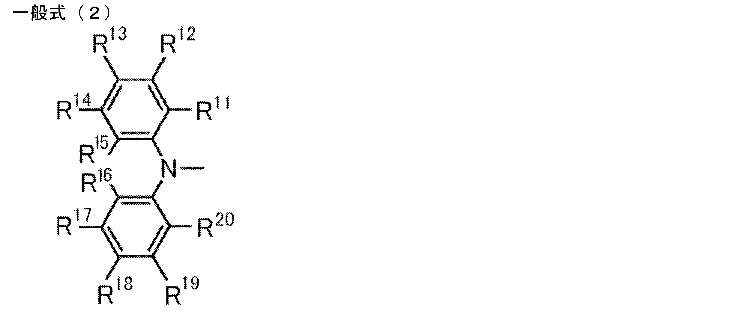
[一般式(2)において、R11~R20は各々独立に水素原子または置換基を表す。R11とR12、R12とR13、R13とR14、R14とR15、R15とR16、R16とR17、R17とR18、R18とR19、R19とR20は互いに結合して環状構造を形成していてもよい。]

[一般式(3)において、R71~R79は各々独立に水素原子または置換基を表す。R71とR72、R72とR73、R73とR74、R74とR75、R76とR77、R77とR78、R78とR79は互いに結合して環状構造を形成していてもよい。]
[2] 前記一般式(2)で表される基が、下記一般式(4)~(8)のいずれかで表される基であることを特徴とする[1]に記載の化合物。
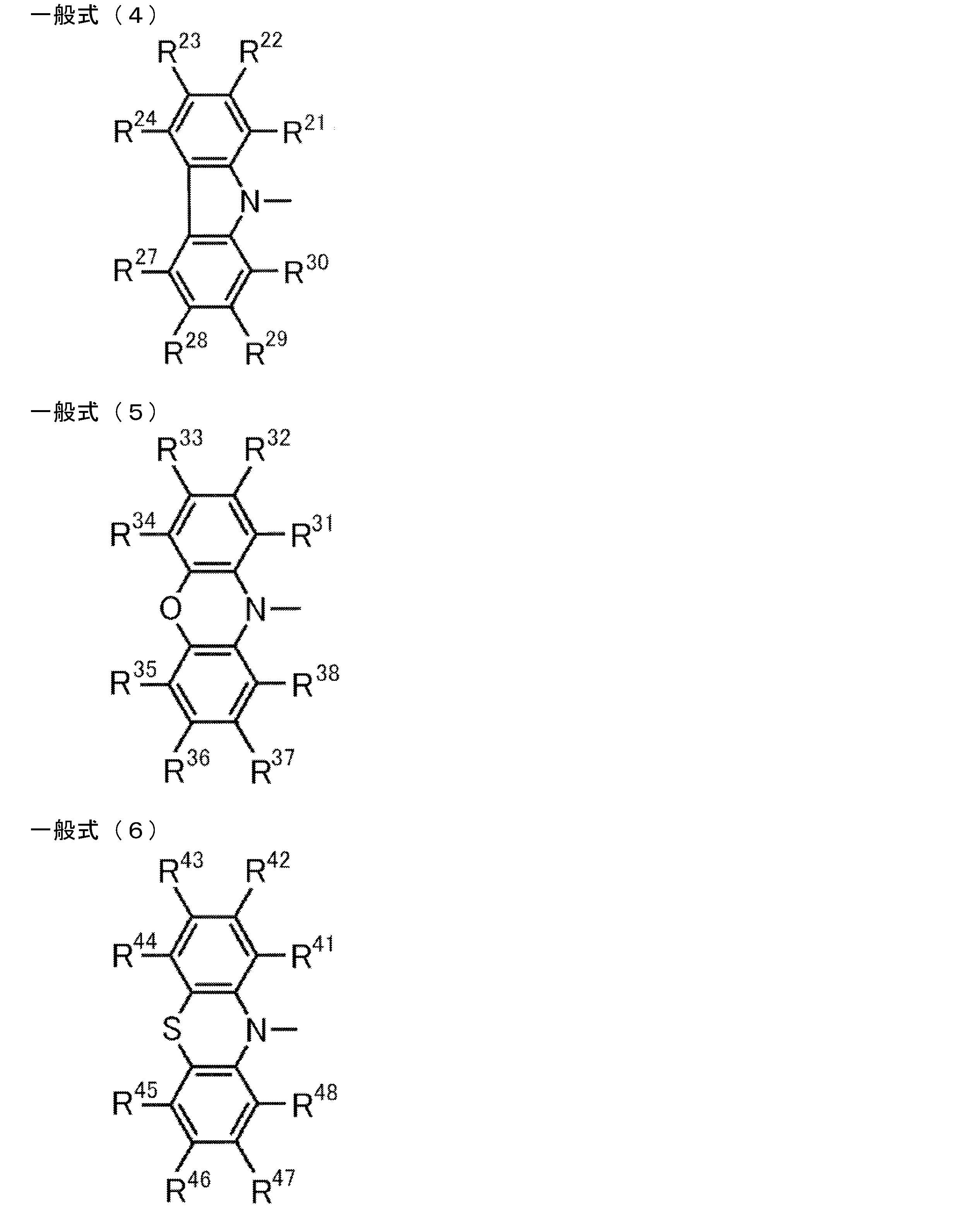
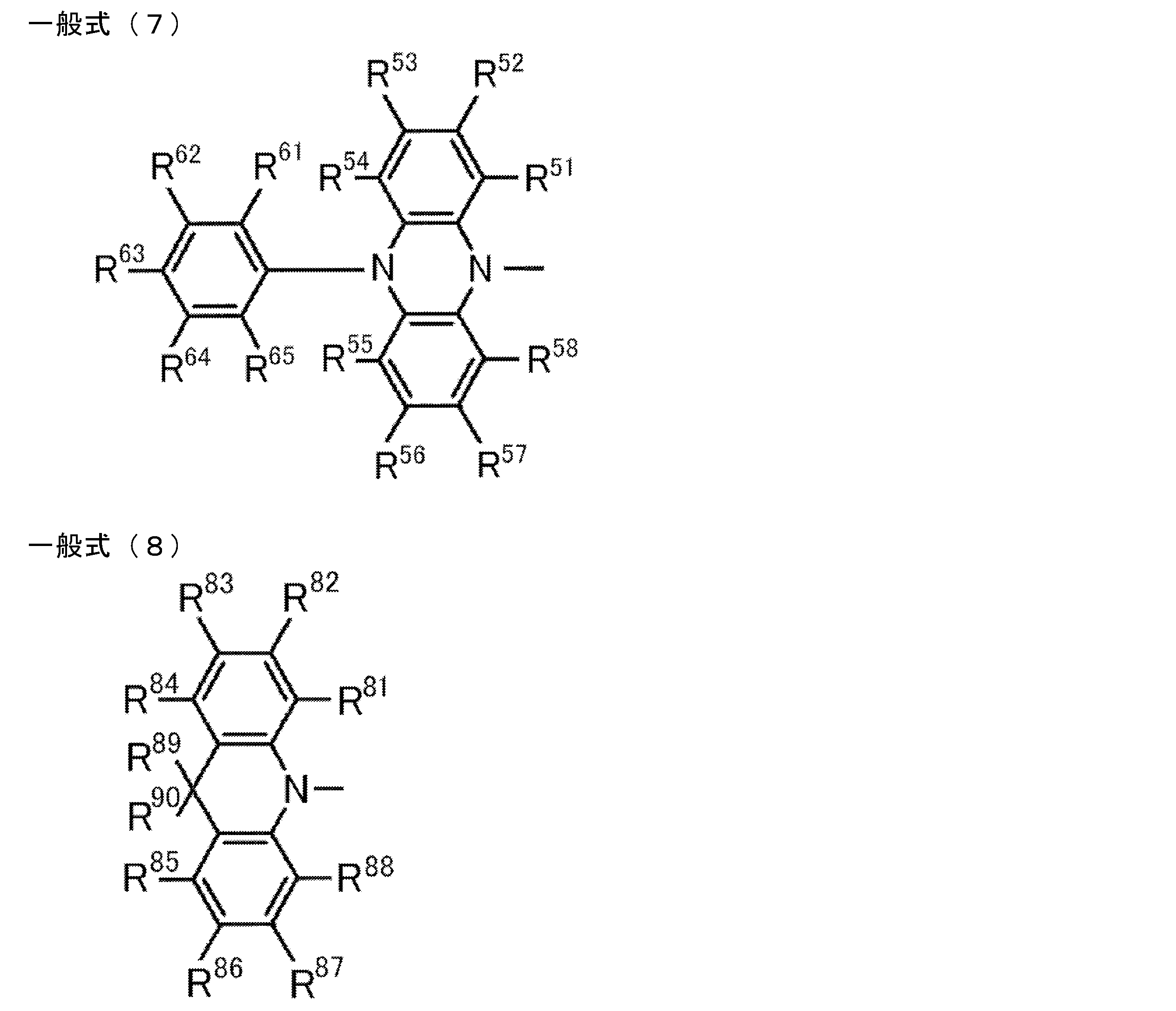
[一般式(4)~(8)において、R21~R24、R27~R38、R41~R48、R51~R58、R61~R65、R81~R90は、各々独立に水素原子または置換基を表す。R21とR22、R22とR23、R23とR24、R27とR28、R28とR29、R29とR30、R31とR32、R32とR33、R33とR34、R35とR36、R36とR37、R37とR38、R41とR42、R42とR43、R43とR44、R45とR46、R46とR47、R47とR48、R51とR52、R52とR53、R53とR54、R55とR56、R56とR57、R57とR58、R61とR62、R62とR63、R63とR64、R64とR65、R54とR61、R55とR65、R81とR82、R82とR83、R83とR84、R85とR86、R86とR87、R87とR88、R89とR90は互いに結合して環状構造を形成していてもよい。]
[3] 前記一般式(1)のR3が、前記一般式(2)で表される基であることを特徴とする[1]または[2]に記載の化合物。
[4] 前記一般式(1)のR1、R2、R4、R5の少なくとも1つは、各々独立に炭素数1~3のアルキル基であることを特徴とする[3]に記載の化合物。
[5] 前記一般式(1)のR1とR5が、前記一般式(2)で表される基であることを特徴とする[1]または[2]に記載の化合物。
[6] 前記一般式(2)で表される基が、前記一般式(8)で表される基であることを特徴とする[1]~[5]のいずれか1項に記載の化合物。
[7] 前記一般式(8)のR89およびR90が、ともに置換もしくは無置換のアリール基であることを特徴とする[6]に記載の化合物。
[2] 前記一般式(2)で表される基が、下記一般式(4)~(8)のいずれかで表される基であることを特徴とする[1]に記載の化合物。
[3] 前記一般式(1)のR3が、前記一般式(2)で表される基であることを特徴とする[1]または[2]に記載の化合物。
[4] 前記一般式(1)のR1、R2、R4、R5の少なくとも1つは、各々独立に炭素数1~3のアルキル基であることを特徴とする[3]に記載の化合物。
[5] 前記一般式(1)のR1とR5が、前記一般式(2)で表される基であることを特徴とする[1]または[2]に記載の化合物。
[6] 前記一般式(2)で表される基が、前記一般式(8)で表される基であることを特徴とする[1]~[5]のいずれか1項に記載の化合物。
[7] 前記一般式(8)のR89およびR90が、ともに置換もしくは無置換のアリール基であることを特徴とする[6]に記載の化合物。
[8] 前記一般式(1)で表される化合物からなる材料と、前記材料にドープされた発光材料を含むことを特徴とする混合物。
[9] 前記一般式(1)で表されるからなる材料と、前記材料にドープされた発光材料を含むことを特徴とする発光層。
[10] 前記一般式(1)で表される化合物は、発光層に含まれる有機化合物の中で最低励起一重項エネルギー準位が最も高い有機化合物であることを特徴とする[9]に記載の発光層。
[11] 前記一般式(1)で表される化合物は、遅延蛍光体であることを特徴とする[9]または[10]に記載の発光層。
[12] 前記一般式(1)で表される化合物は、最低励起一重項状態と77Kの最低励起三重項状態とのエネルギーの差ΔEstが0.3eV以下であることを特徴とする[11]に記載の発光層。
[13] さらに、ホストを含むことを特徴とする[9]に記載の発光層。
[14] 前記ホストと前記一般式(1)で表される化合物と前記発光材料が下記式(A)を満たし、且つ前記一般式(1)で表される化合物が遅延蛍光体であることを特徴とする[13]に記載の発光層。
式(A) ES1(A)>ES1(B)>ES1(C)
[上式において、ES1(A)はホストの最低励起一重項エネルギー準位を表し、ES1(B)は一般式(1)で表される化合物の最低励起一重項エネルギー準位を表し、ES1(C)は発光材料の最低励起一重項エネルギー準位を表す。]
[15] 前記一般式(1)で表される化合物は、最低励起一重項状態と77Kの最低励起三重項状態とのエネルギーの差ΔEstが0.3eV以下であることを特徴とする[14]に記載の発光層。
[10] 前記一般式(1)で表される化合物は、発光層に含まれる有機化合物の中で最低励起一重項エネルギー準位が最も高い有機化合物であることを特徴とする[9]に記載の発光層。
[11] 前記一般式(1)で表される化合物は、遅延蛍光体であることを特徴とする[9]または[10]に記載の発光層。
[12] 前記一般式(1)で表される化合物は、最低励起一重項状態と77Kの最低励起三重項状態とのエネルギーの差ΔEstが0.3eV以下であることを特徴とする[11]に記載の発光層。
[13] さらに、ホストを含むことを特徴とする[9]に記載の発光層。
[14] 前記ホストと前記一般式(1)で表される化合物と前記発光材料が下記式(A)を満たし、且つ前記一般式(1)で表される化合物が遅延蛍光体であることを特徴とする[13]に記載の発光層。
式(A) ES1(A)>ES1(B)>ES1(C)
[上式において、ES1(A)はホストの最低励起一重項エネルギー準位を表し、ES1(B)は一般式(1)で表される化合物の最低励起一重項エネルギー準位を表し、ES1(C)は発光材料の最低励起一重項エネルギー準位を表す。]
[15] 前記一般式(1)で表される化合物は、最低励起一重項状態と77Kの最低励起三重項状態とのエネルギーの差ΔEstが0.3eV以下であることを特徴とする[14]に記載の発光層。
[16] [9]~[15]のいずれか1項に記載の発光層を有することを特徴とする有機発光素子。
[17] 有機エレクトロルミネッセンス素子であることを特徴とする[16]に記載の有機発光素子。
[17] 有機エレクトロルミネッセンス素子であることを特徴とする[16]に記載の有機発光素子。
[18] 下記一般式(1)で表される化合物からなることを特徴とするアシストドーパント。
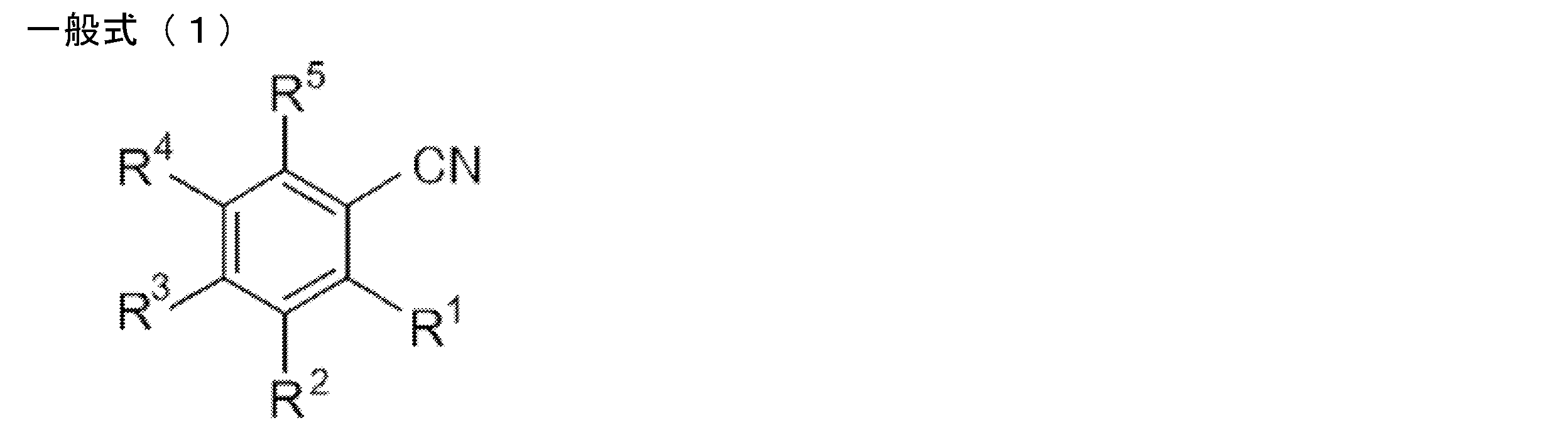
[一般式(1)において、R1~R5は各々独立に水素原子、またはシアノ基以外の置換基を表し、R1~R5の少なくとも1つは各々独立に下記一般式(2)または下記一般式(3)で表される基である。]

[一般式(2)において、R11~R20は各々独立に水素原子または置換基を表す。R11とR12、R12とR13、R13とR14、R14とR15、R15とR16、R16とR17、R17とR18、R18とR19、R19とR20は互いに結合して環状構造を形成していてもよい。]
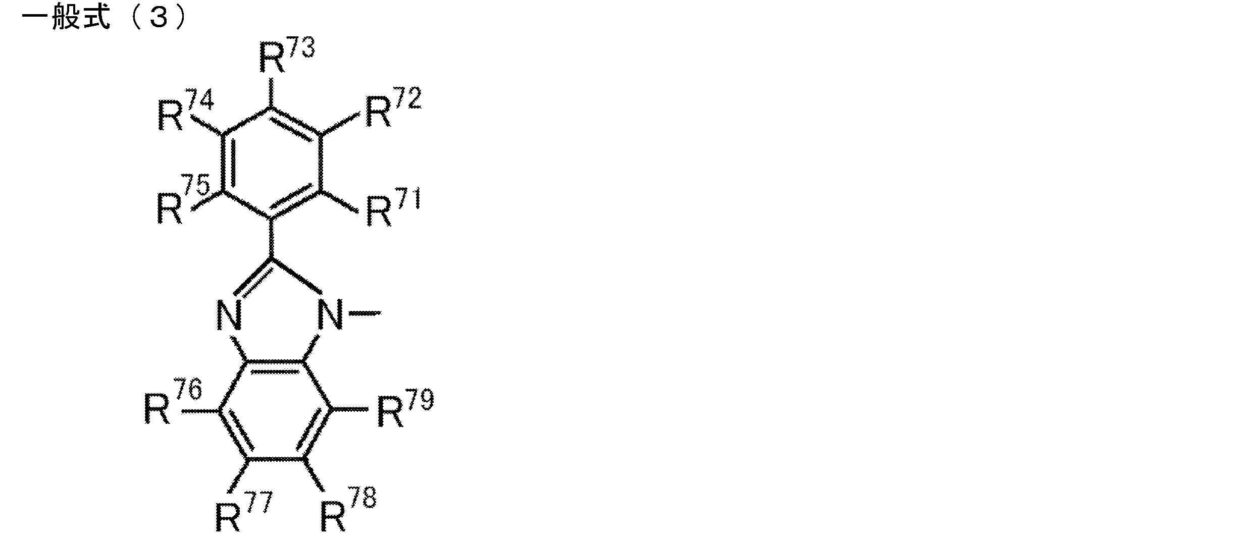
[一般式(3)において、R71~R79は各々独立に水素原子または置換基を表す。R71とR72、R72とR73、R73とR74、R74とR75、R76とR77、R77とR78、R78とR79は互いに結合して環状構造を形成していてもよい。]
本発明の化合物は、ホストおよびアシストドーパントとして有用である。本発明の化合物をホストまたはアシストドーパントとして用いた有機発光素子は、高い発光効率を実現しうる。
以下において、本発明の内容について詳細に説明する。以下に記載する構成要件の説明は、本発明の代表的な実施態様や具体例に基づいてなされることがあるが、本発明はそのような実施態様や具体例に限定されるものではない。なお、本明細書において「~」を用いて表される数値範囲は、「~」の前後に記載される数値を下限値および上限値として含む範囲を意味する。また、本発明に用いられる化合物の分子内に存在する水素原子の同位体種は特に限定されず、例えば分子内の水素原子がすべて1Hであってもよいし、一部または全部が2H(デューテリウムD)であってもよい。
[一般式(1)で表される化合物]
本発明の化合物は、下記一般式(1)で表される化合物である。
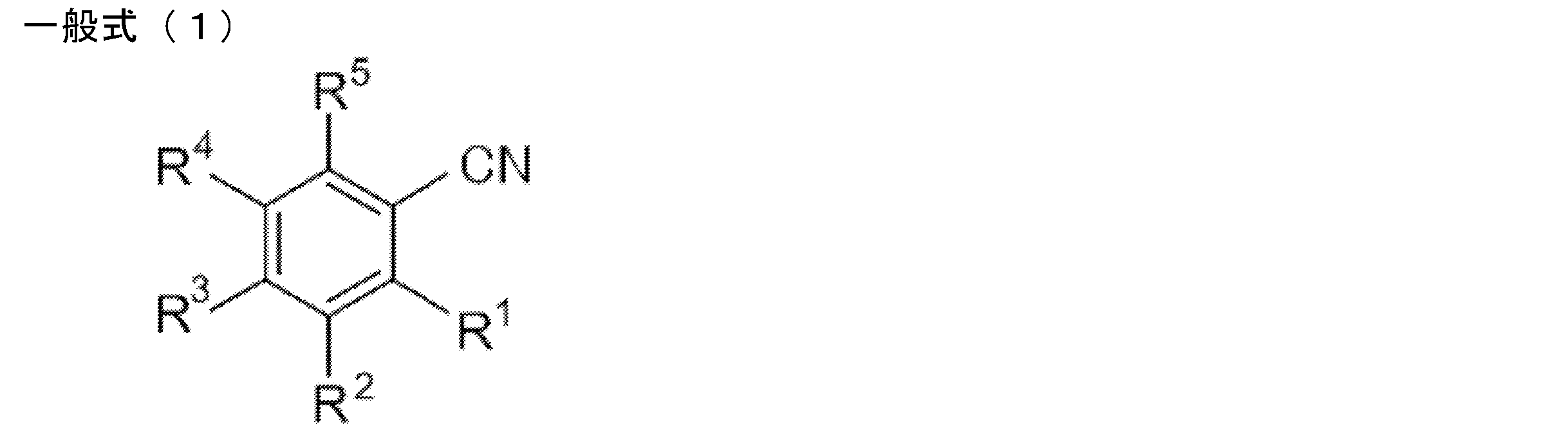
本発明の化合物は、下記一般式(1)で表される化合物である。
一般式(1)において、R1~R5は各々独立に水素原子、またはシアノ基以外の置換基を表し、R1~R5の少なくとも1つは各々独立に下記一般式(2)または下記一般式(3)で表される基である。
一般式(2)または(3)で表される基は、R1~R5のうちの1つのみであってもよいし、2~5つであってもよいが、1つまたは2つであることが好ましい。
一般式(2)または(3)で表される基がR1~R5のうちの1つのみであるときは、R2またはR3が一般式(2)または(3)で表される基であることが好ましく、R3が一般式(2)または(3)で表される基であることが好ましい。
R1~R5のうちの2つが一般式(2)または(3)で表される基であるときは、R1またはR2と、R4またはR5が一般式(2)または(3)で表される基であることが好ましく、R1とR5が一般式(2)または(3)で表される基であることがより好ましい。また、R1~R5のうちの3つが一般式(2)または(3)で表される基であるときは、R1、R3、R5が一般式(2)または(3)で表される基であることが好ましい。また、R1~R5のうちの4つが一般式(2)または(3)で表される基であるときは、R1、R2、R4、R5が一般式(2)または(3)で表される基であることが好ましい。
一般式(2)または(3)で表される基は、R1~R5のうちの1つのみであってもよいし、2~5つであってもよいが、1つまたは2つであることが好ましい。
一般式(2)または(3)で表される基がR1~R5のうちの1つのみであるときは、R2またはR3が一般式(2)または(3)で表される基であることが好ましく、R3が一般式(2)または(3)で表される基であることが好ましい。
R1~R5のうちの2つが一般式(2)または(3)で表される基であるときは、R1またはR2と、R4またはR5が一般式(2)または(3)で表される基であることが好ましく、R1とR5が一般式(2)または(3)で表される基であることがより好ましい。また、R1~R5のうちの3つが一般式(2)または(3)で表される基であるときは、R1、R3、R5が一般式(2)または(3)で表される基であることが好ましい。また、R1~R5のうちの4つが一般式(2)または(3)で表される基であるときは、R1、R2、R4、R5が一般式(2)または(3)で表される基であることが好ましい。
R11~R20、R71~R79がとりうる置換基として、例えばヒドロキシ基、ハロゲン原子、シアノ基、炭素数1~20のアルキル基、炭素数1~20のアルコキシ基、炭素数1~20のアルキルチオ基、炭素数1~20のアルキル置換アミノ基、炭素数2~20のアシル基、炭素数6~40のアリール基、炭素数3~40のヘテロアリール基、炭素数2~10のアルケニル基、炭素数2~10のアルキニル基、炭素数2~10のアルコキシカルボニル基、炭素数1~10のアルキルスルホニル基、炭素数1~10のハロアルキル基、アミド基、炭素数2~10のアルキルアミド基、炭素数3~20のトリアルキルシリル基、炭素数4~20のトリアルキルシリルアルキル基、炭素数5~20のトリアルキルシリルアルケニル基、炭素数5~20のトリアルキルシリルアルキニル基およびニトロ基等が挙げられる。これらの具体例のうち、さらに置換基により置換可能なものは置換されていてもよい。より好ましい置換基は、ハロゲン原子、シアノ基、炭素数1~20の置換もしくは無置換のアルキル基、炭素数1~20のアルコキシ基、炭素数6~40の置換もしくは無置換のアリール基、炭素数3~40の置換もしくは無置換のヘテロアリール基、炭素数1~20のジアルキル置換アミノ基である。さらに好ましい置換基は、フッ素原子、塩素原子、シアノ基、炭素数1~10の置換もしくは無置換のアルキル基、炭素数1~10の置換もしくは無置換のアルコキシ基、炭素数6~15の置換もしくは無置換のアリール基、炭素数3~12の置換もしくは無置換のヘテロアリール基である。
R11とR12、R12とR13、R13とR14、R14とR15、R15とR16、R16とR17、R17とR18、R18とR19、R19とR20、R71とR72、R72とR73、R73とR74、R74とR75、R76とR77、R77とR78、R78とR79は互いに結合して環状構造を形成していてもよい。環状構造は芳香環であっても脂肪環であってもよく、またヘテロ原子を含むものであってもよく、さらに環状構造は2環以上の縮合環であってもよい。ここでいうヘテロ原子としては、窒素原子、酸素原子および硫黄原子からなる群より選択されるものであることが好ましい。形成される環状構造の例として、ベンゼン環、ナフタレン環、ピリジン環、ピリダジン環、ピリミジン環、ピラジン環、ピロール環、イミダゾール環、ピラゾール環、トリアゾール環、イミダゾリン環、オキサゾール環、イソオキサゾール環、チアゾール環、イソチアゾール環、シクロヘキサジエン環、シクロヘキセン環、シクロペンタエン環、シクロヘプタトリエン環、シクロヘプタジエン環、シクロヘプタエン環などを挙げることができる。
一般式(2)で表される基は、下記一般式(4)~(8)のいずれかで表される基であることが好ましく、一般式(8)で表される基であることがより好ましい。
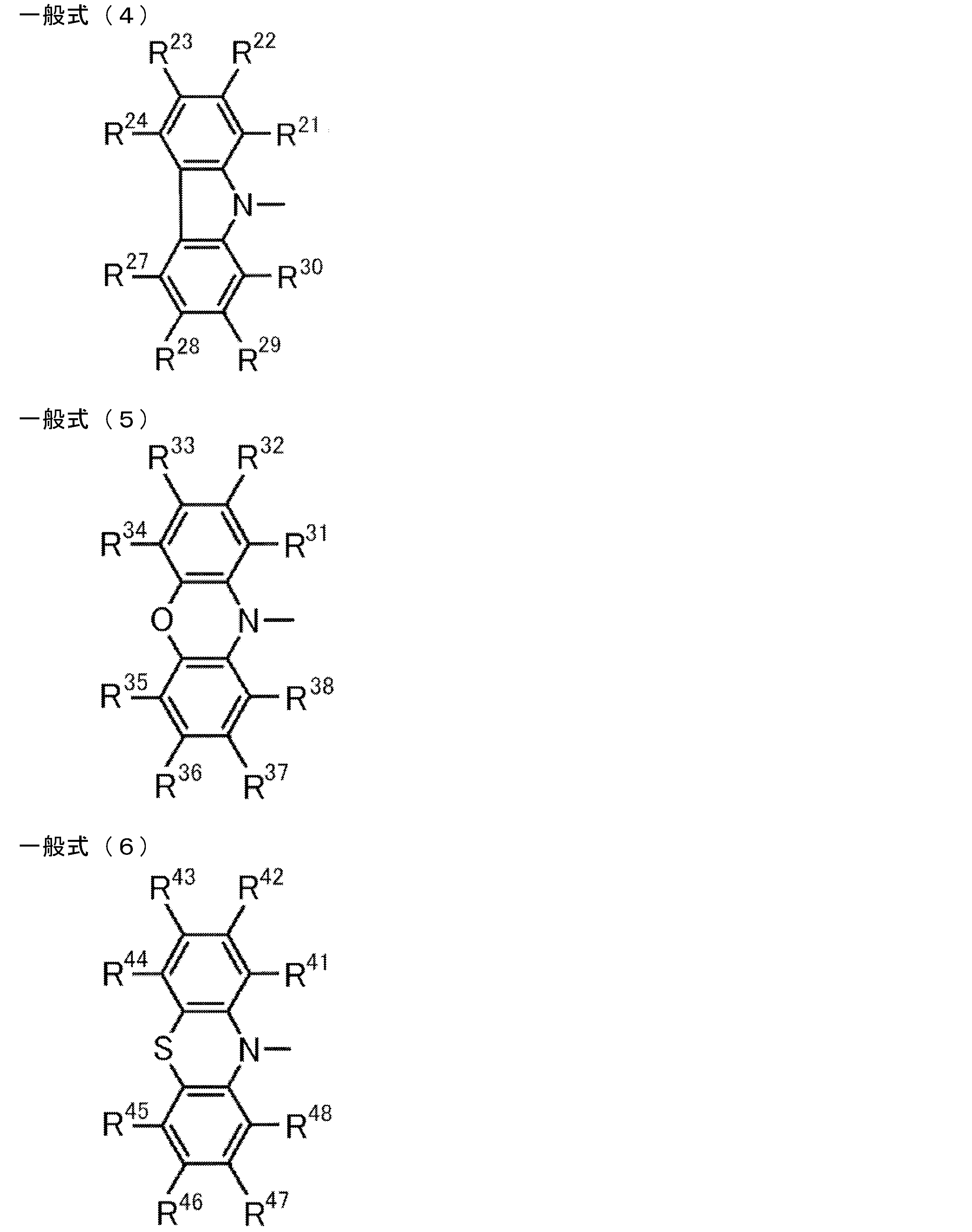
一般式(4)~(8)において、R21~R24、R27~R38、R41~R48、R51~R58、R61~R65、R81~R90は、各々独立に水素原子または置換基を表す。ここでいう置換基の説明と好ましい範囲については、上記のR11~R20がとりうる置換基の説明と好ましい範囲を参照することができる。一般式(4)~(8)における置換基の数は特に制限されない。R21~R24、R27~R38、R41~R48、R51~R58、R61~R65、R81~R90と上記のR71~R79は、各々独立に上記一般式(3)~(8)のいずれかで表される基であることも好ましい。すべてが無置換(すなわち水素原子)である場合も好ましい。また、一般式(4)~(8)のそれぞれにおいて置換基が2つ以上ある場合、それらの置換基は同一であっても異なっていてもよい。
また、一般式(4)~(8)に置換基が存在している場合、その置換基は一般式(4)であればR22~R24、R27~R29のいずれかであることが好ましく、R23およびR28の少なくとも1つであることがより好ましく、一般式(5)であればR32~R37のいずれかであることが好ましく、一般式(6)であればR42~R47のいずれかであることが好ましく、一般式(7)であればR52、R53、R56、R57、R62~R64のいずれかであることが好ましく、一般式(8)であればR82~R87、R89、R90のいずれかであることが好ましく、R89およびR90であることが好ましい。R89およびR90が表す置換基は、炭素数6~40の置換もしくは無置換のアリール基であることが好ましく、置換もしくは無置換のフェニル基であることがより好ましい。また、R89およびR90が表す置換基は同一であることが好ましい。
また、一般式(4)~(8)に置換基が存在している場合、その置換基は一般式(4)であればR22~R24、R27~R29のいずれかであることが好ましく、R23およびR28の少なくとも1つであることがより好ましく、一般式(5)であればR32~R37のいずれかであることが好ましく、一般式(6)であればR42~R47のいずれかであることが好ましく、一般式(7)であればR52、R53、R56、R57、R62~R64のいずれかであることが好ましく、一般式(8)であればR82~R87、R89、R90のいずれかであることが好ましく、R89およびR90であることが好ましい。R89およびR90が表す置換基は、炭素数6~40の置換もしくは無置換のアリール基であることが好ましく、置換もしくは無置換のフェニル基であることがより好ましい。また、R89およびR90が表す置換基は同一であることが好ましい。
一般式(4)~(8)において、R21とR22、R22とR23、R23とR24、R27とR28、R28とR29、R29とR30、R31とR32、R32とR33、R33とR34、R35とR36、R36とR37、R37とR38、R41とR42、R42とR43、R43とR44、R45とR46、R46とR47、R47とR48、R51とR52、R52とR53、R53とR54、R55とR56、R56とR57、R57とR58、R61とR62、R62とR63、R63とR64、R64とR65、R54とR61、R55とR65、R81とR82、R82とR83、R83とR84、R85とR86、R86とR87、R87とR88、R89とR90は互いに結合して環状構造を形成していてもよい。環状構造の説明と好ましい例については、上記の一般式(2)において、R11とR12等が互いに結合して形成する環状構造の説明と好ましい例を参照することができる。
一般式(1)中に存在する一般式(2)で表される基は、すべてが一般式(4)~(8)のいずれか1つの一般式で表される基であることが好ましい。例えば、すべてが一般式(8)で表される基を好ましく例示することができる。
R1~R5のうち一般式(2)または(3)で表される基以外は各々独立に水素原子、またはシアノ基以外の置換基である。一般式(2)または(3)で表される基以外にR1~R5がとる置換基の数は特に制限されず、一般式(2)または(3)で表される基以外はすべて無置換(すなわち水素原子)であってもよい。一般式(2)または(3)で表される基以外にR1~R5の2つ以上が置換基をとる場合、複数の置換基は互いに同一であっても異なっていてもよい。
R1~R5がとりうる置換基の説明と好ましい範囲については、シアノ基を除いた上記のR11~R20がとりうる置換基の説明と好ましい範囲を参照することができる。このうち、R3が一般式(2)で表される基または(3)で表される基であるとき、R1、R2、R4、R5の少なくとも1つは炭素数1~20のアルキル基であることが好ましく、R1、R2、R4、R5の全てが炭素数1~20のアルキル基であることがより好ましい。このアルキル基の炭素数は、1~10であることが好ましく、1~6であることがより好ましく、1~3であることがさらに好ましい。
R1~R5がとりうる置換基の説明と好ましい範囲については、シアノ基を除いた上記のR11~R20がとりうる置換基の説明と好ましい範囲を参照することができる。このうち、R3が一般式(2)で表される基または(3)で表される基であるとき、R1、R2、R4、R5の少なくとも1つは炭素数1~20のアルキル基であることが好ましく、R1、R2、R4、R5の全てが炭素数1~20のアルキル基であることがより好ましい。このアルキル基の炭素数は、1~10であることが好ましく、1~6であることがより好ましく、1~3であることがさらに好ましい。
以下において、一般式(1)で表される化合物の具体例を例示する。ただし、本発明において用いることができる一般式(1)で表される化合物はこれらの具体例によって限定的に解釈されるべきものではない。
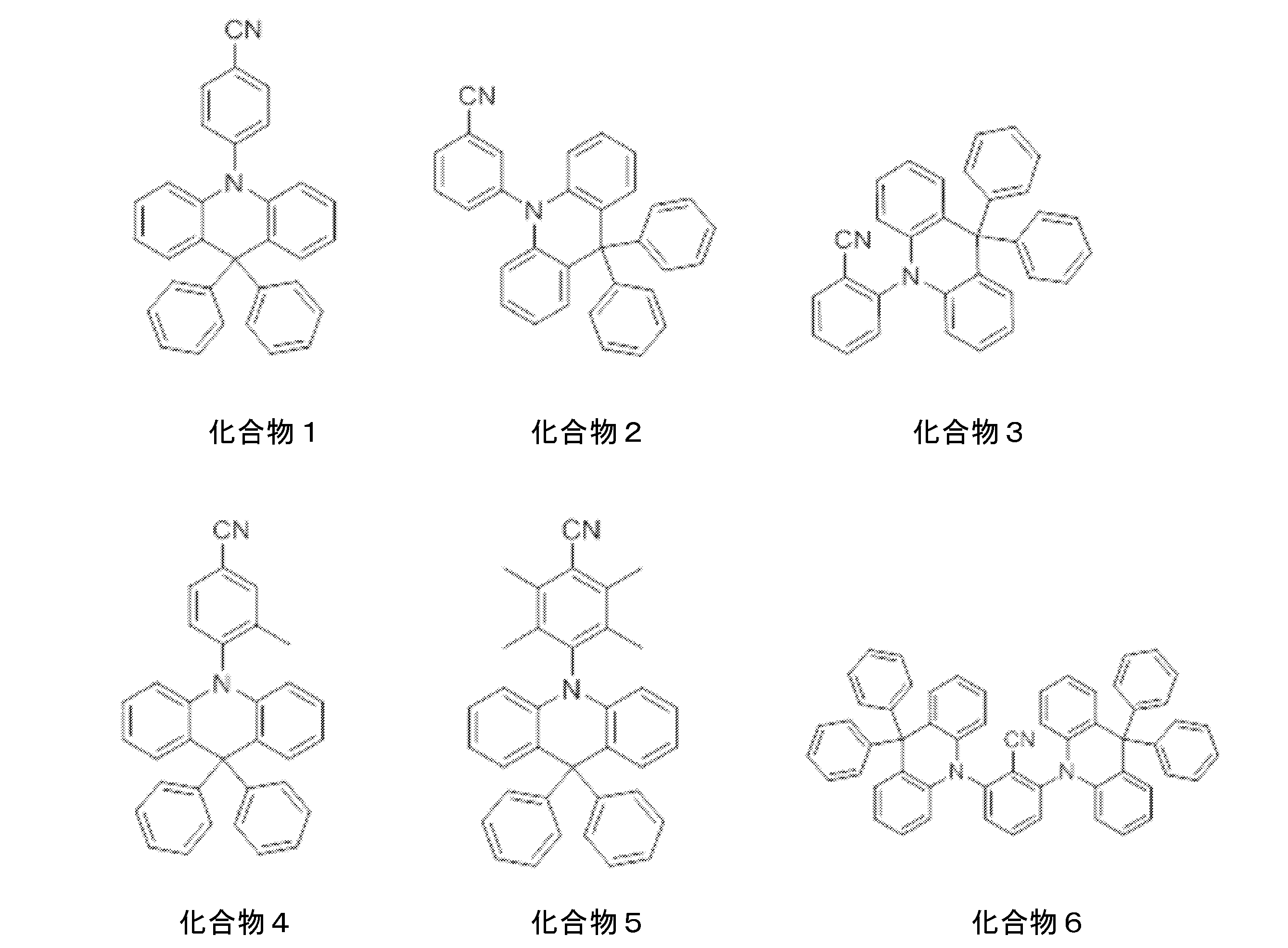
一般式(1)で表される化合物の分子量は、例えば一般式(1)で表される化合物を含む有機層を蒸着法により製膜して利用することを意図する場合には、1500以下であることが好ましく、1200以下であることがより好ましく、1000以下であることがさらに好ましく、800以下であることがさらにより好ましい。分子量の下限値は、一般式(1)で表される最小化合物の分子量である。
一般式(1)で表される化合物は、分子量にかかわらず塗布法で成膜してもよい。塗布法を用いれば、分子量が比較的大きな化合物であっても成膜することが可能である。
一般式(1)で表される化合物は、発光層のホストおよびアシストドーパントとして有用である。また、本発明を応用して、分子内に一般式(1)で表される構造を複数個含む化合物を、ホストまたはアシストドーパントとして用いることも考えられる。
一般式(1)で表される化合物は、分子量にかかわらず塗布法で成膜してもよい。塗布法を用いれば、分子量が比較的大きな化合物であっても成膜することが可能である。
一般式(1)で表される化合物は、発光層のホストおよびアシストドーパントとして有用である。また、本発明を応用して、分子内に一般式(1)で表される構造を複数個含む化合物を、ホストまたはアシストドーパントとして用いることも考えられる。
例えば、一般式(1)で表される構造中にあらかじめ重合性基を存在させておいて、その重合性基を重合させることによって得られる重合体を、ホストおよびアシストドーパントとして用いることが考えられる。具体的には、一般式(1)のR1~R5のいずれかに重合性官能基を含むモノマーを用意して、これを単独で重合させるか、他のモノマーとともに共重合させることにより、繰り返し単位を有する重合体を得て、その重合体をホストおよびアシストドーパントとして用いることが考えられる。あるいは、一般式(1)で表される構造を有する化合物どうしを反応させることにより、二量体や三量体を得て、それらをホストおよびアシストドーパントとして用いることも考えられる。
一般式(1)で表される構造を含む繰り返し単位を有する重合体の例として、下記一般式(9)または(10)で表される構造を含む重合体を挙げることができる。

一般式(1)で表される構造を含む繰り返し単位を有する重合体の例として、下記一般式(9)または(10)で表される構造を含む重合体を挙げることができる。
一般式(9)または(10)において、Qは一般式(1)で表される構造を含む基を表し、L1およびL2は連結基を表す。連結基の炭素数は、好ましくは0~20であり、より好ましくは1~15であり、さらに好ましくは2~10である。連結基は-X11-L11-で表される構造を有するものであることが好ましい。ここで、X11は酸素原子または硫黄原子を表し、酸素原子であることが好ましい。L11は連結基を表し、置換もしくは無置換のアルキレン基、または置換もしくは無置換のアリーレン基であることが好ましく、炭素数1~10の置換もしくは無置換のアルキレン基、または置換もしくは無置換のフェニレン基であることがより好ましい。
一般式(9)または(10)において、R101、R102、R103およびR104は、各々独立に置換基を表す。好ましくは、炭素数1~6の置換もしくは無置換のアルキル基、炭素数1~6の置換もしくは無置換のアルコキシ基、ハロゲン原子であり、より好ましくは炭素数1~3の無置換のアルキル基、炭素数1~3の無置換のアルコキシ基、フッ素原子、塩素原子であり、さらに好ましくは炭素数1~3の無置換のアルキル基、炭素数1~3の無置換のアルコキシ基である。
L1およびL2で表される連結基は、Qを構成する一般式(1)の構造のR1~R5のいずれか、一般式(2)のR11~R20のいずれか、一般式(3)の構造のR71~R78のいずれか、一般式(4)の構造のR21~R24、R27~R30のいずれか、一般式(5)の構造のR31~R38のいずれか、一般式(6)の構造のR41~R48のいずれか、一般式(7)の構造のR51~R58、R61~R65のいずれか、一般式(8)の構造のR81~R90のいずれかに結合することができる。1つのQに対して連結基が2つ以上連結して架橋構造や網目構造を形成していてもよい。
一般式(9)または(10)において、R101、R102、R103およびR104は、各々独立に置換基を表す。好ましくは、炭素数1~6の置換もしくは無置換のアルキル基、炭素数1~6の置換もしくは無置換のアルコキシ基、ハロゲン原子であり、より好ましくは炭素数1~3の無置換のアルキル基、炭素数1~3の無置換のアルコキシ基、フッ素原子、塩素原子であり、さらに好ましくは炭素数1~3の無置換のアルキル基、炭素数1~3の無置換のアルコキシ基である。
L1およびL2で表される連結基は、Qを構成する一般式(1)の構造のR1~R5のいずれか、一般式(2)のR11~R20のいずれか、一般式(3)の構造のR71~R78のいずれか、一般式(4)の構造のR21~R24、R27~R30のいずれか、一般式(5)の構造のR31~R38のいずれか、一般式(6)の構造のR41~R48のいずれか、一般式(7)の構造のR51~R58、R61~R65のいずれか、一般式(8)の構造のR81~R90のいずれかに結合することができる。1つのQに対して連結基が2つ以上連結して架橋構造や網目構造を形成していてもよい。
繰り返し単位の具体的な構造例として、下記式(11)~(14)で表される構造を挙げることができる。

これらの式(11)~(14)を含む繰り返し単位を有する重合体は、一般式(1)の構造のR1~R5のいずれかにヒドロキシ基を導入しておき、それをリンカーとして下記化合物を反応させて重合性基を導入し、その重合性基を重合させることにより合成することができる。
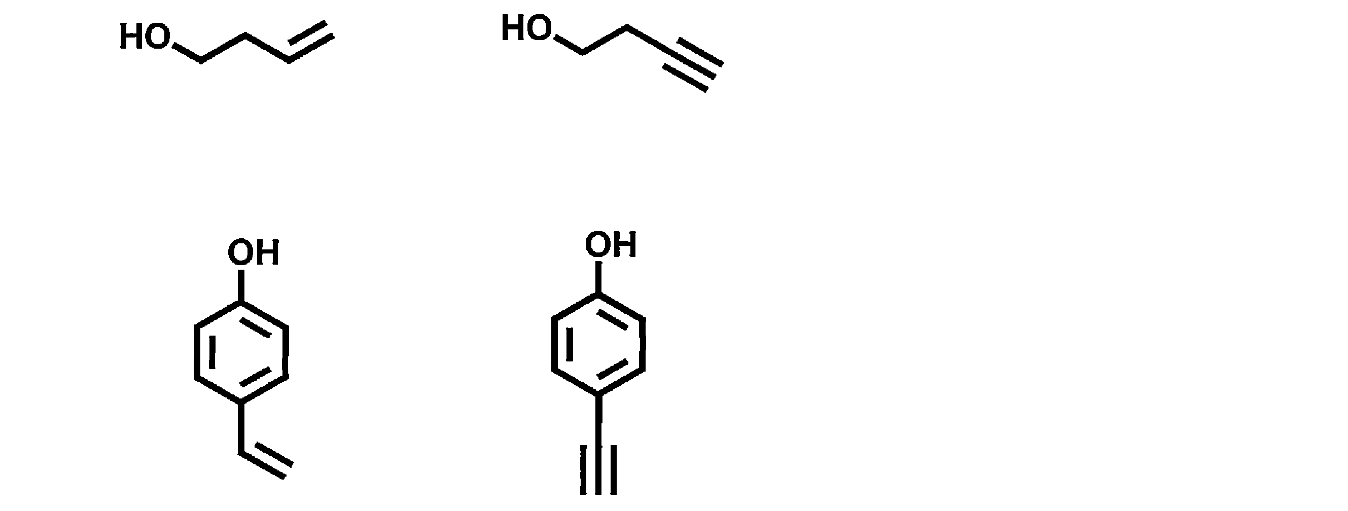
分子内に一般式(1)で表される構造を含む重合体は、一般式(1)で表される構造を有する繰り返し単位のみからなる重合体であってもよいし、それ以外の構造を有する繰り返し単位を含む重合体であってもよい。また、重合体の中に含まれる一般式(1)で表される構造を有する繰り返し単位は、単一種であってもよいし、2種以上であってもよい。一般式(1)で表される構造を有さない繰り返し単位としては、通常の共重合に用いられるモノマーから誘導されるものを挙げることができる。例えば、エチレン、スチレンなどのエチレン性不飽和結合を有するモノマーから誘導される繰り返し単位を挙げることができる。
[一般式(1)で表される化合物の合成方法]
一般式(1)で表される化合物は、既知の反応を組み合わせることによって合成することができる。例えば、一般式(1)のR3が一般式(2)で表される基である化合物は、以下の2つの化合物を反応させることにより合成することが可能である。

一般式(1)で表される化合物は、既知の反応を組み合わせることによって合成することができる。例えば、一般式(1)のR3が一般式(2)で表される基である化合物は、以下の2つの化合物を反応させることにより合成することが可能である。
上記の反応式におけるR1、R2、R4、R5、R11~R20の説明については、一般式(1)における対応する記載を参照することができる。Xはハロゲン原子を表し、フッ素原子、塩素原子、臭素原子、ヨウ素原子を挙げることができ、塩素原子、臭素原子、ヨウ素原子が好ましい。
上記の反応は、公知のカップリング反応を応用したものであり、公知の反応条件を適宜選択して用いることができる。上記の反応の詳細については、後述の合成例を参考にすることができる。また、一般式(1)で表される化合物は、その他の公知の合成反応を組み合わせることによっても合成することができる。
上記の反応は、公知のカップリング反応を応用したものであり、公知の反応条件を適宜選択して用いることができる。上記の反応の詳細については、後述の合成例を参考にすることができる。また、一般式(1)で表される化合物は、その他の公知の合成反応を組み合わせることによっても合成することができる。
[混合物]
本発明の一般式(1)で表される化合物は、該化合物からなる材料に発光材料がドープされた混合物を構成することができる。こうした混合物は、例えば有機発光素子の発光層の材料として好適に用いることができる。
混合物において、一般式(1)で表される化合物は1種類を単独で用いてもよいし、2種類以上を組み合わせて用いてもよい。
発光材料は、赤色発光材料、緑色発光材料、青色発光材料のいずれであってもよく、2色または3色の発光材料を混合したものであってもよい。また、赤色発光材料、緑色発光材料、青色発光材料は、それぞれ1種類の有機化合物からなっていてもよいし、2種類以上の有機化合物を組み合わせたものであってもよい。
混合物における一般式(1)で表される化合物の含有量は、発光材料の含有量よりも大きな量とされる。これらの含有量の好ましい範囲については、下記の発光層における一般式(1)で表される化合物と発光材料の含有量についての記載を参照することができる。
混合物は、一般式(1)で表される化合物および発光材料以外の有機化合物を含んでいてもよい。
発光材料の具体例、一般式(1)で表される化合物および発光材料以外に用いることができる有機化合物の具体例については、下記の発光層に用いられる発光材料およびその他の有機化合物の具体例を参照することができる。
本発明の一般式(1)で表される化合物は、該化合物からなる材料に発光材料がドープされた混合物を構成することができる。こうした混合物は、例えば有機発光素子の発光層の材料として好適に用いることができる。
混合物において、一般式(1)で表される化合物は1種類を単独で用いてもよいし、2種類以上を組み合わせて用いてもよい。
発光材料は、赤色発光材料、緑色発光材料、青色発光材料のいずれであってもよく、2色または3色の発光材料を混合したものであってもよい。また、赤色発光材料、緑色発光材料、青色発光材料は、それぞれ1種類の有機化合物からなっていてもよいし、2種類以上の有機化合物を組み合わせたものであってもよい。
混合物における一般式(1)で表される化合物の含有量は、発光材料の含有量よりも大きな量とされる。これらの含有量の好ましい範囲については、下記の発光層における一般式(1)で表される化合物と発光材料の含有量についての記載を参照することができる。
混合物は、一般式(1)で表される化合物および発光材料以外の有機化合物を含んでいてもよい。
発光材料の具体例、一般式(1)で表される化合物および発光材料以外に用いることができる有機化合物の具体例については、下記の発光層に用いられる発光材料およびその他の有機化合物の具体例を参照することができる。
[有機発光素子]
本発明の一般式(1)で表される化合物は、有機発光素子のホストおよびアシストドーパントとして有用である。このため、本発明の一般式(1)で表される化合物は、有機発光素子の発光層にホストまたはアシストドーパントとして効果的に用いることができ、これにより発光効率が高い有機発光素子を実現することができる。
ここで、本発明において「ホスト」とは、発光材料とともに発光層に含まれる有機化合物であって、発光層に含まれる有機化合物のうち最低励起一重項エネルギー準位が最も高い有機化合物のことをいう。また、「アシストドーパント」とは、少なくとも該アシストドーパントとホストと発光材料を含む発光層において、アシストドーパントを含まないこと以外は同じ組成の発光層よりも発光材料の発光効率が高くなるように作用する有機化合物のことをいう。
以下において、一般式(1)で表される化合物と発光材料を発光層に含む有機発光素子(本発明の有機発光素子)について具体的に説明する。
本発明の一般式(1)で表される化合物は、有機発光素子のホストおよびアシストドーパントとして有用である。このため、本発明の一般式(1)で表される化合物は、有機発光素子の発光層にホストまたはアシストドーパントとして効果的に用いることができ、これにより発光効率が高い有機発光素子を実現することができる。
ここで、本発明において「ホスト」とは、発光材料とともに発光層に含まれる有機化合物であって、発光層に含まれる有機化合物のうち最低励起一重項エネルギー準位が最も高い有機化合物のことをいう。また、「アシストドーパント」とは、少なくとも該アシストドーパントとホストと発光材料を含む発光層において、アシストドーパントを含まないこと以外は同じ組成の発光層よりも発光材料の発光効率が高くなるように作用する有機化合物のことをいう。
以下において、一般式(1)で表される化合物と発光材料を発光層に含む有機発光素子(本発明の有機発光素子)について具体的に説明する。
本発明の有機発光素子は、有機フォトルミネッセンス素子(有機PL素子)であってもよいし、有機エレクトロルミネッセンス素子(有機EL素子)であってもよい。
有機フォトルミネッセンス素子は、基板上に少なくとも発光層を形成した構造を有する。また、有機エレクトロルミネッセンス素子は、少なくとも陽極、陰極、および陽極と陰極の間に有機層を形成した構造を有する。有機層は、少なくとも発光層を含むものであり、発光層のみからなるものであってもよいし、発光層の他に1層以上の有機層を有するものであってもよい。そのような他の有機層として、正孔輸送層、正孔注入層、電子阻止層、正孔阻止層、電子注入層、電子輸送層、励起子阻止層などを挙げることができる。正孔輸送層は正孔注入機能を有した正孔注入輸送層でもよく、電子輸送層は電子注入機能を有した電子注入輸送層でもよい。具体的な有機エレクトロルミネッセンス素子の構造例を図1に示す。図1において、1は基板、2は陽極、3は正孔注入層、4は正孔輸送層、5は発光層、6は電子輸送層、7は陰極を表わす。
以下では、有機エレクトロルミネッセンス素子の各部材および各層について説明する。なお、基板と発光層の説明は有機フォトルミネッセンス素子の基板と発光層にも該当する。
有機フォトルミネッセンス素子は、基板上に少なくとも発光層を形成した構造を有する。また、有機エレクトロルミネッセンス素子は、少なくとも陽極、陰極、および陽極と陰極の間に有機層を形成した構造を有する。有機層は、少なくとも発光層を含むものであり、発光層のみからなるものであってもよいし、発光層の他に1層以上の有機層を有するものであってもよい。そのような他の有機層として、正孔輸送層、正孔注入層、電子阻止層、正孔阻止層、電子注入層、電子輸送層、励起子阻止層などを挙げることができる。正孔輸送層は正孔注入機能を有した正孔注入輸送層でもよく、電子輸送層は電子注入機能を有した電子注入輸送層でもよい。具体的な有機エレクトロルミネッセンス素子の構造例を図1に示す。図1において、1は基板、2は陽極、3は正孔注入層、4は正孔輸送層、5は発光層、6は電子輸送層、7は陰極を表わす。
以下では、有機エレクトロルミネッセンス素子の各部材および各層について説明する。なお、基板と発光層の説明は有機フォトルミネッセンス素子の基板と発光層にも該当する。
[発光層]
発光層は、陽極および陰極のそれぞれから注入された正孔および電子が再結合することにより励起子が生成した後、発光する層である。
本発明の有機発光素子では、発光層は、一般式(1)で表される化合物と発光材料を含有する。一般式(1)で表される化合物は、ホストとして用いてもよいし、アシストドーパントとして用いてもよい。
(一般式(1)で表される化合物をホストとして用いる系)
一般式(1)で表される化合物をホストとして用いる発光層は、一般式(1)で表される化合物からなるホストに発光材料がドープされて形成され、且つ、一般式(1)で表される化合物が、発光層を構成する有機化合物のうちで最低励起一重項エネルギー準位が最も高くなるように構成される。これにより、正孔と電子の再結合によって一般式(1)で表される化合物で生成された励起一重項エネルギーが、発光材料に容易に移動して発光材料中に閉じ込められ、発光材料の発光に効果的に寄与するものと推測される。その結果、高い発光効率を得ることができる。
発光層は、陽極および陰極のそれぞれから注入された正孔および電子が再結合することにより励起子が生成した後、発光する層である。
本発明の有機発光素子では、発光層は、一般式(1)で表される化合物と発光材料を含有する。一般式(1)で表される化合物は、ホストとして用いてもよいし、アシストドーパントとして用いてもよい。
(一般式(1)で表される化合物をホストとして用いる系)
一般式(1)で表される化合物をホストとして用いる発光層は、一般式(1)で表される化合物からなるホストに発光材料がドープされて形成され、且つ、一般式(1)で表される化合物が、発光層を構成する有機化合物のうちで最低励起一重項エネルギー準位が最も高くなるように構成される。これにより、正孔と電子の再結合によって一般式(1)で表される化合物で生成された励起一重項エネルギーが、発光材料に容易に移動して発光材料中に閉じ込められ、発光材料の発光に効果的に寄与するものと推測される。その結果、高い発光効率を得ることができる。
ホストとして用いる一般式(1)で表される化合物は、遅延蛍光体であることが好ましい。これにより、発光効率をより高くすることができる。ここで、本明細書中において「遅延蛍光体」とは、励起三重項状態に遷移した後、励起一重項状態に逆項間交差することができ、励起一重項状態から基底状態に戻るときに蛍光を放射する有機化合物のことを言う。なお、励起三重項状態から励起一重項状態への逆項間交差により生じる光の寿命は、通常の蛍光(即時蛍光)や燐光よりも長くなるため、これらよりも遅延した蛍光として観察される。一般式(1)で表される化合物が遅延蛍光体である場合に、高い発光効率が得られるのは下記の理由によるものと推測される。
すなわち、発光層のホスト分子上で正孔と電子が再結合すると、ホストが基底状態から励起一重項状態と励起三重項状態に励起されるが、ホストが遅延蛍光体である場合、励起三重項状態に励起されたホスト分子は逆項間交差を通じて励起一重項状態に遷移する。このため、正孔と電子の再結合によって直接生成された励起一重項エネルギーとともに、励起三重項エネルギーも逆項間交差を通じて励起一重項エネルギーとして利用することができる。そして、この両方の励起一重項エネルギーが発光材料に移動して発光材料を発光させるため、高い発光効率が得られるものと推測される。
すなわち、発光層のホスト分子上で正孔と電子が再結合すると、ホストが基底状態から励起一重項状態と励起三重項状態に励起されるが、ホストが遅延蛍光体である場合、励起三重項状態に励起されたホスト分子は逆項間交差を通じて励起一重項状態に遷移する。このため、正孔と電子の再結合によって直接生成された励起一重項エネルギーとともに、励起三重項エネルギーも逆項間交差を通じて励起一重項エネルギーとして利用することができる。そして、この両方の励起一重項エネルギーが発光材料に移動して発光材料を発光させるため、高い発光効率が得られるものと推測される。
発光層に含まれる一般式(1)で表される化合物と発光材料の含有量は特に限定されないが、ホストである一般式(1)で表される化合物の含有量は発光材料の含有量よりも大きいことが好ましい。具体的には、一般式(1)で表される化合物の含有量と発光材料の含有量の合計質量を100質量%としたとき、一般式(1)で表される化合物の含有量は、50質量%以上、99.9質量%以下であることが好ましく、発光材料の含有量は、0.1質量%以上、50質量%以下であることがより好ましい。
(一般式(1)で表される化合物をアシストドーパントとして用いる系)
一般式(1)で表される化合物をアシストドーパントとして用いる発光層は、ホストに、一般式(1)で表される化合物からなるアシストドーパントと発光材料がドープされて構成される。ここで、ホストは、一般式(1)で表される化合物および発光材料以外の有機化合物であって、発光層に含まれる有機化合物のうち最低励起一重項エネルギー準位が最も高い有機化合物である。
一般式(1)で表される化合物をアシストドーパントとして用いる発光層は、ホストに、一般式(1)で表される化合物からなるアシストドーパントと発光材料がドープされて構成される。ここで、ホストは、一般式(1)で表される化合物および発光材料以外の有機化合物であって、発光層に含まれる有機化合物のうち最低励起一重項エネルギー準位が最も高い有機化合物である。
一般式(1)で表される化合物をアシストドーパントとして用いる系では、一般式(1)で表される化合物が遅延蛍光体であって、ホスト材料と一般式(1)で表される化合物と発光材料とが下記式(A)を満たすことが好ましい。
式(A) ES1(A)>ES1(B)>ES1(C)
上式において、ES1(A)はホストの最低励起一重項エネルギー準位を表し、ES1(B)はアシストドーパントである一般式(1)で表される化合物の最低励起一重項エネルギー準位を表し、ES1(C)は発光材料の最低励起一重項エネルギー準位を表す。
これにより、一般式(1)で表される化合物を効果的にアシストドーパントとして機能させることができ、発光効率をさらに高くすることができる。これは、以下の理由によるものと推測される。
すなわち、発光層において、正孔と電子の再結合によって励起エネルギーが発生すると、発光層に含まれる各化合物が基底状態から励起一重項状態と励起三重項状態に励起される。このとき、ホストとアシストドーパントである一般式(1)で表される化合物と発光材料とが式(A)を満たしていると、ホストと一般式(1)で表される化合物の励起一重項エネルギーが容易に発光材料に移動し、基底状態の発光材料が励起一重項状態に遷移する。励起一重項状態になった発光材料は、その後基底状態に戻るときに蛍光を放射(放射失活)する。
ここで、遅延蛍光体である一般式(1)で表される化合物では、励起三重項状態に励起された分子が逆項間交差を通じて励起一重項状態に遷移する。このため、正孔と電子の再結合によって直接生成された励起一重項エネルギーとともに、励起三重項エネルギーも逆項間交差を通じて励起一重項エネルギーとして利用することができる。そして、この両方の励起一重項エネルギーとホストで生成された励起一重項エネルギーが発光材料に移動して発光材料の発光に寄与するため、さらに高い発光効率が得られるものと推測される。
式(A) ES1(A)>ES1(B)>ES1(C)
上式において、ES1(A)はホストの最低励起一重項エネルギー準位を表し、ES1(B)はアシストドーパントである一般式(1)で表される化合物の最低励起一重項エネルギー準位を表し、ES1(C)は発光材料の最低励起一重項エネルギー準位を表す。
これにより、一般式(1)で表される化合物を効果的にアシストドーパントとして機能させることができ、発光効率をさらに高くすることができる。これは、以下の理由によるものと推測される。
すなわち、発光層において、正孔と電子の再結合によって励起エネルギーが発生すると、発光層に含まれる各化合物が基底状態から励起一重項状態と励起三重項状態に励起される。このとき、ホストとアシストドーパントである一般式(1)で表される化合物と発光材料とが式(A)を満たしていると、ホストと一般式(1)で表される化合物の励起一重項エネルギーが容易に発光材料に移動し、基底状態の発光材料が励起一重項状態に遷移する。励起一重項状態になった発光材料は、その後基底状態に戻るときに蛍光を放射(放射失活)する。
ここで、遅延蛍光体である一般式(1)で表される化合物では、励起三重項状態に励起された分子が逆項間交差を通じて励起一重項状態に遷移する。このため、正孔と電子の再結合によって直接生成された励起一重項エネルギーとともに、励起三重項エネルギーも逆項間交差を通じて励起一重項エネルギーとして利用することができる。そして、この両方の励起一重項エネルギーとホストで生成された励起一重項エネルギーが発光材料に移動して発光材料の発光に寄与するため、さらに高い発光効率が得られるものと推測される。
一般式(1)で表される化合物をアシストドーパントとして用いる系では、ホストと一般式(1)で表される化合物は、さらに、下記の式(B)を満たすことが好ましい。これにより、一段と高い発光効率を実現することができる。
式(B) ET1(A)>ET1(B)
上式において、ET1(A)はホストの77Kにおける最低励起三重項エネルギー準位を表し、ET1(B)はアシストドーパントである一般式(1)で表される化合物の77Kにおける最低励起三重項エネルギー準位を表す。一般式(1)で表される化合物の77Kにおける最低励起三重項エネルギー準位ET1(B)と、発光材料の77Kにおける最低励起三重項エネルギー準位ET1(C)の関係は特に制限されないが、例えばET1(B)>ET1(C)となるように選択してもよい。
ホストと一般式(1)で表される化合物が式(B)を満たしていると、ホストで生成された励起三重項エネルギーが一般式(1)で表される化合物に容易に移動し、該化合物が励起三重項状態に励起される。そして、上記のように、遅延蛍光体である一般式(1)で表される化合物では、励起三重項状態に励起された分子が逆項間交差を通じて励起一重項状態に遷移するため、結果として、ホストで生成された励起三重項エネルギーも励起一重項エネルギーとして発光材料の発光に効果的に寄与するものと推測される。これにより、さらに高い発光効率を得ることができる。
式(B) ET1(A)>ET1(B)
上式において、ET1(A)はホストの77Kにおける最低励起三重項エネルギー準位を表し、ET1(B)はアシストドーパントである一般式(1)で表される化合物の77Kにおける最低励起三重項エネルギー準位を表す。一般式(1)で表される化合物の77Kにおける最低励起三重項エネルギー準位ET1(B)と、発光材料の77Kにおける最低励起三重項エネルギー準位ET1(C)の関係は特に制限されないが、例えばET1(B)>ET1(C)となるように選択してもよい。
ホストと一般式(1)で表される化合物が式(B)を満たしていると、ホストで生成された励起三重項エネルギーが一般式(1)で表される化合物に容易に移動し、該化合物が励起三重項状態に励起される。そして、上記のように、遅延蛍光体である一般式(1)で表される化合物では、励起三重項状態に励起された分子が逆項間交差を通じて励起一重項状態に遷移するため、結果として、ホストで生成された励起三重項エネルギーも励起一重項エネルギーとして発光材料の発光に効果的に寄与するものと推測される。これにより、さらに高い発光効率を得ることができる。
発光層に含まれるホストと一般式(1)で表される化合物と発光材料の含有量は、特に限定されないが、一般式(1)で表される化合物の含有量はホストの含有量よりも小さいことが好ましい。これにより、より高い発光効率を得ることができる。具体的には、ホストの含有量W1と一般式(1)で表される化合物の含有量W2と発光材料の含有量W3の合計重量を100重量%としたとき、ホストの含有量W1は15重量%以上、99.9重量%以下であることが好ましく、一般式(1)で表される化合物の含有量W2は5.0重量%以上、50重量%以下であることが好ましく、発光材料の含有量W3は0.5重量%以上、5.0重量%以下であることが好ましい。
上記のように、一般式(1)で表される化合物は、ホストとして用いる場合とアシストドーパントとして用いる場合のいずれにおいても遅延蛍光体であることが好ましい。この遅延蛍光体は、熱エネルギーの吸収によって励起一重項状態から励起三重項状態に逆項間交差する熱活性化型の遅延蛍光体であることが好ましい。熱活性化型の遅延蛍光体は、デバイスが発する熱を吸収して励起三重項状態から励起一重項へ比較的容易に逆項間交差し、その励起三重項エネルギーを効率よく発光に寄与させることができる。
遅延蛍光体である一般式(1)で表される化合物は、最低励起一重項状態でのエネルギー準位Es1と77Kの最低励起三重項状態でのエネルギー準位ET1の差ΔEstが0.3eV以下であることが好ましく、0.2eV以下であることがより好ましく、0.1eV以下であることがさらに好ましく、0.08eV以下であることがさらにより好ましい。エネルギー差ΔEstが前記範囲の遅延蛍光体は、励起三重項状態から励起一重項状態への逆項間交差が比較的容易に起こり、その励起三重項エネルギーを効率よく発光に寄与させることができる。
遅延蛍光体である一般式(1)で表される化合物は、最低励起一重項状態でのエネルギー準位Es1と77Kの最低励起三重項状態でのエネルギー準位ET1の差ΔEstが0.3eV以下であることが好ましく、0.2eV以下であることがより好ましく、0.1eV以下であることがさらに好ましく、0.08eV以下であることがさらにより好ましい。エネルギー差ΔEstが前記範囲の遅延蛍光体は、励起三重項状態から励起一重項状態への逆項間交差が比較的容易に起こり、その励起三重項エネルギーを効率よく発光に寄与させることができる。
一般式(1)で表される化合物をホストとして用いる系と一般式(1)で表される化合物をアシストドーパントとして用いる系で使用する発光材料は、公知の発光材料を用いることができ、少なくとも蛍光を放射し得る発光材料であることが好ましく、蛍光とともに遅延蛍光や燐光を放射するものであってもよい。例えば、下記の化合物を好ましく用いることができる。

一般式(1)で表される化合物をアシストドーパンとして用いる系で使用するホストは、発光層に含まれる有機化合物の中で最低励起一重項エネルギー準位が最も高いということ以外は特に制限されず、発光層で一般的に用いられているホストを用いることができる。中でも、正孔輸送能、電子輸送能を有し、かつ発光の長波長化を防ぎ、なおかつ高いガラス転移温度を有する有機化合物であることが好ましい。
なお、本発明の有機エレクトロルミネッセンス素子において、発光は主として発光材料から生じるが、発光の一部あるいは部分的に一般式(1)で表される化合物やホストからの発光であってもかまわない。また、この発光は、少なくとも蛍光発光であり、遅延蛍光発光や燐光発光を含んでいてもよい。
(その他の有機化合物)
一般式(1)で表される化合物をホストとして用いる系では、発光層は一般式(1)で表される化合物と発光材料のみから構成されていてもよいし、その他の有機化合物を含んでいてもよい。
また、一般式(1)で表される化合物をアシストドーパントとして用いる系では、発光層は一般式(1)で表される化合物と発光材料とホストのみから構成されていてもよいし、その他の有機化合物を含んでいてもよい。その他の有機化合物としては、例えば正孔輸送能を有する有機化合物、電子輸送能を有する有機化合物等を挙げることができる。正孔輸送能を有する有機化合物、電子輸送能を有する有機化合物としては、下記の正孔輸送材料、電子輸送材料をそれぞれ参照することができる。
一般式(1)で表される化合物をホストとして用いる系では、発光層は一般式(1)で表される化合物と発光材料のみから構成されていてもよいし、その他の有機化合物を含んでいてもよい。
また、一般式(1)で表される化合物をアシストドーパントとして用いる系では、発光層は一般式(1)で表される化合物と発光材料とホストのみから構成されていてもよいし、その他の有機化合物を含んでいてもよい。その他の有機化合物としては、例えば正孔輸送能を有する有機化合物、電子輸送能を有する有機化合物等を挙げることができる。正孔輸送能を有する有機化合物、電子輸送能を有する有機化合物としては、下記の正孔輸送材料、電子輸送材料をそれぞれ参照することができる。
[基板]
本発明の有機エレクトロルミネッセンス素子は、基板に支持されていることが好ましい。この基板については、特に制限はなく、従来から有機エレクトロルミネッセンス素子に慣用されているものであればよく、例えば、ガラス、透明プラスチック、石英、シリコンなどからなるものを用いることができる。
本発明の有機エレクトロルミネッセンス素子は、基板に支持されていることが好ましい。この基板については、特に制限はなく、従来から有機エレクトロルミネッセンス素子に慣用されているものであればよく、例えば、ガラス、透明プラスチック、石英、シリコンなどからなるものを用いることができる。
[陽極]
有機エレクトロルミネッセンス素子における陽極としては、仕事関数の大きい(4eV以上)金属、合金、電気伝導性化合物およびこれらの混合物を電極材料とするものが好ましく用いられる。このような電極材料の具体例としてはAu等の金属、CuI、インジウムチンオキシド(ITO)、SnO2、ZnO等の導電性透明材料が挙げられる。また、IDIXO(In2O3-ZnO)等非晶質で透明導電膜を作製可能な材料を用いてもよい。陽極はこれらの電極材料を蒸着やスパッタリング等の方法により、薄膜を形成させ、フォトリソグラフィー法で所望の形状のパターンを形成してもよく、あるいはパターン精度をあまり必要としない場合は(100μm以上程度)、上記電極材料の蒸着やスパッタリング時に所望の形状のマスクを介してパターンを形成してもよい。あるいは、有機導電性化合物のように塗布可能な材料を用いる場合には、印刷方式、コーティング方式等湿式成膜法を用いることもできる。この陽極より発光を取り出す場合には、透過率を10%より大きくすることが望ましく、また陽極としてのシート抵抗は数百Ω/□以下が好ましい。さらに膜厚は材料にもよるが、通常10~1000nm、好ましくは10~200nmの範囲で選ばれる。
有機エレクトロルミネッセンス素子における陽極としては、仕事関数の大きい(4eV以上)金属、合金、電気伝導性化合物およびこれらの混合物を電極材料とするものが好ましく用いられる。このような電極材料の具体例としてはAu等の金属、CuI、インジウムチンオキシド(ITO)、SnO2、ZnO等の導電性透明材料が挙げられる。また、IDIXO(In2O3-ZnO)等非晶質で透明導電膜を作製可能な材料を用いてもよい。陽極はこれらの電極材料を蒸着やスパッタリング等の方法により、薄膜を形成させ、フォトリソグラフィー法で所望の形状のパターンを形成してもよく、あるいはパターン精度をあまり必要としない場合は(100μm以上程度)、上記電極材料の蒸着やスパッタリング時に所望の形状のマスクを介してパターンを形成してもよい。あるいは、有機導電性化合物のように塗布可能な材料を用いる場合には、印刷方式、コーティング方式等湿式成膜法を用いることもできる。この陽極より発光を取り出す場合には、透過率を10%より大きくすることが望ましく、また陽極としてのシート抵抗は数百Ω/□以下が好ましい。さらに膜厚は材料にもよるが、通常10~1000nm、好ましくは10~200nmの範囲で選ばれる。
[陰極]
一方、陰極としては、仕事関数の小さい(4eV以下)金属(電子注入性金属と称する)、合金、電気伝導性化合物およびこれらの混合物を電極材料とするものが用いられる。このような電極材料の具体例としては、ナトリウム、ナトリウム-カリウム合金、マグネシウム、リチウム、マグネシウム/銅混合物、マグネシウム/銀混合物、マグネシウム/アルミニウム混合物、マグネシウム/インジウム混合物、アルミニウム/酸化アルミニウム(Al2O3)混合物、インジウム、リチウム/アルミニウム混合物、希土類金属等が挙げられる。これらの中で、電子注入性および酸化等に対する耐久性の点から、電子注入性金属とこれより仕事関数の値が大きく安定な金属である第二金属との混合物、例えば、マグネシウム/銀混合物、マグネシウム/アルミニウム混合物、マグネシウム/インジウム混合物、アルミニウム/酸化アルミニウム(Al2O3)混合物、リチウム/アルミニウム混合物、アルミニウム等が好適である。陰極はこれらの電極材料を蒸着やスパッタリング等の方法により薄膜を形成させることにより、作製することができる。また、陰極としてのシート抵抗は数百Ω/□以下が好ましく、膜厚は通常10nm~5μm、好ましくは50~200nmの範囲で選ばれる。なお、発光した光を透過させるため、有機エレクトロルミネッセンス素子の陽極または陰極のいずれか一方が、透明または半透明であれば発光輝度が向上し好都合である。
また、陽極の説明で挙げた導電性透明材料を陰極に用いることで、透明または半透明の陰極を作製することができ、これを応用することで陽極と陰極の両方が透過性を有する素子を作製することができる。
一方、陰極としては、仕事関数の小さい(4eV以下)金属(電子注入性金属と称する)、合金、電気伝導性化合物およびこれらの混合物を電極材料とするものが用いられる。このような電極材料の具体例としては、ナトリウム、ナトリウム-カリウム合金、マグネシウム、リチウム、マグネシウム/銅混合物、マグネシウム/銀混合物、マグネシウム/アルミニウム混合物、マグネシウム/インジウム混合物、アルミニウム/酸化アルミニウム(Al2O3)混合物、インジウム、リチウム/アルミニウム混合物、希土類金属等が挙げられる。これらの中で、電子注入性および酸化等に対する耐久性の点から、電子注入性金属とこれより仕事関数の値が大きく安定な金属である第二金属との混合物、例えば、マグネシウム/銀混合物、マグネシウム/アルミニウム混合物、マグネシウム/インジウム混合物、アルミニウム/酸化アルミニウム(Al2O3)混合物、リチウム/アルミニウム混合物、アルミニウム等が好適である。陰極はこれらの電極材料を蒸着やスパッタリング等の方法により薄膜を形成させることにより、作製することができる。また、陰極としてのシート抵抗は数百Ω/□以下が好ましく、膜厚は通常10nm~5μm、好ましくは50~200nmの範囲で選ばれる。なお、発光した光を透過させるため、有機エレクトロルミネッセンス素子の陽極または陰極のいずれか一方が、透明または半透明であれば発光輝度が向上し好都合である。
また、陽極の説明で挙げた導電性透明材料を陰極に用いることで、透明または半透明の陰極を作製することができ、これを応用することで陽極と陰極の両方が透過性を有する素子を作製することができる。
[注入層]
注入層とは、駆動電圧低下や発光輝度向上のために電極と有機層間に設けられる層のことで、正孔注入層と電子注入層があり、陽極と発光層または正孔輸送層の間、および陰極と発光層または電子輸送層との間に存在させてもよい。注入層は必要に応じて設けることができる。
注入層とは、駆動電圧低下や発光輝度向上のために電極と有機層間に設けられる層のことで、正孔注入層と電子注入層があり、陽極と発光層または正孔輸送層の間、および陰極と発光層または電子輸送層との間に存在させてもよい。注入層は必要に応じて設けることができる。
[阻止層]
阻止層は、発光層中に存在する電荷(電子もしくは正孔)および/または励起子の発光層外への拡散を阻止することができる層である。電子阻止層は、発光層および正孔輸送層の間に配置されることができ、電子が正孔輸送層の方に向かって発光層を通過することを阻止する。同様に、正孔阻止層は発光層および電子輸送層の間に配置されることができ、正孔が電子輸送層の方に向かって発光層を通過することを阻止する。阻止層はまた、励起子が発光層の外側に拡散することを阻止するために用いることができる。すなわち電子阻止層、正孔阻止層はそれぞれ励起子阻止層としての機能も兼ね備えることができる。本明細書でいう電子阻止層または励起子阻止層は、一つの層で電子阻止層および励起子阻止層の機能を有する層を含む意味で使用される。
阻止層は、発光層中に存在する電荷(電子もしくは正孔)および/または励起子の発光層外への拡散を阻止することができる層である。電子阻止層は、発光層および正孔輸送層の間に配置されることができ、電子が正孔輸送層の方に向かって発光層を通過することを阻止する。同様に、正孔阻止層は発光層および電子輸送層の間に配置されることができ、正孔が電子輸送層の方に向かって発光層を通過することを阻止する。阻止層はまた、励起子が発光層の外側に拡散することを阻止するために用いることができる。すなわち電子阻止層、正孔阻止層はそれぞれ励起子阻止層としての機能も兼ね備えることができる。本明細書でいう電子阻止層または励起子阻止層は、一つの層で電子阻止層および励起子阻止層の機能を有する層を含む意味で使用される。
[正孔阻止層]
正孔阻止層とは広い意味では電子輸送層の機能を有する。正孔阻止層は電子を輸送しつつ、正孔が電子輸送層へ到達することを阻止する役割があり、これにより発光層中での電子と正孔の再結合確率を向上させることができる。正孔阻止層の材料としては、後述する電子輸送層の材料を必要に応じて用いることができる。
正孔阻止層とは広い意味では電子輸送層の機能を有する。正孔阻止層は電子を輸送しつつ、正孔が電子輸送層へ到達することを阻止する役割があり、これにより発光層中での電子と正孔の再結合確率を向上させることができる。正孔阻止層の材料としては、後述する電子輸送層の材料を必要に応じて用いることができる。
電子阻止層]
電子阻止層とは、広い意味では正孔を輸送する機能を有する。電子阻止層は正孔を輸送しつつ、電子が正孔輸送層へ到達することを阻止する役割があり、これにより発光層中での電子と正孔が再結合する確率を向上させることができる。
電子阻止層とは、広い意味では正孔を輸送する機能を有する。電子阻止層は正孔を輸送しつつ、電子が正孔輸送層へ到達することを阻止する役割があり、これにより発光層中での電子と正孔が再結合する確率を向上させることができる。
[励起子阻止層]
励起子阻止層とは、発光層内で正孔と電子が再結合することにより生じた励起子が電荷輸送層に拡散することを阻止するための層であり、本層の挿入により励起子を効率的に発光層内に閉じ込めることが可能となり、素子の発光効率を向上させることができる。励起子阻止層は発光層に隣接して陽極側、陰極側のいずれにも挿入することができ、両方同時に挿入することも可能である。すなわち、励起子阻止層を陽極側に有する場合、正孔輸送層と発光層の間に、発光層に隣接して該層を挿入することができ、陰極側に挿入する場合、発光層と陰極との間に、発光層に隣接して該層を挿入することができる。また、陽極と、発光層の陽極側に隣接する励起子阻止層との間には、正孔注入層や電子阻止層などを有することができ、陰極と、発光層の陰極側に隣接する励起子阻止層との間には、電子注入層、電子輸送層、正孔阻止層などを有することができる。阻止層を配置する場合、阻止層として用いる材料の励起一重項エネルギーおよび励起三重項エネルギーの少なくともいずれか一方は、発光材料の励起一重項エネルギーおよび励起三重項エネルギーよりも高いことが好ましい。
励起子阻止層とは、発光層内で正孔と電子が再結合することにより生じた励起子が電荷輸送層に拡散することを阻止するための層であり、本層の挿入により励起子を効率的に発光層内に閉じ込めることが可能となり、素子の発光効率を向上させることができる。励起子阻止層は発光層に隣接して陽極側、陰極側のいずれにも挿入することができ、両方同時に挿入することも可能である。すなわち、励起子阻止層を陽極側に有する場合、正孔輸送層と発光層の間に、発光層に隣接して該層を挿入することができ、陰極側に挿入する場合、発光層と陰極との間に、発光層に隣接して該層を挿入することができる。また、陽極と、発光層の陽極側に隣接する励起子阻止層との間には、正孔注入層や電子阻止層などを有することができ、陰極と、発光層の陰極側に隣接する励起子阻止層との間には、電子注入層、電子輸送層、正孔阻止層などを有することができる。阻止層を配置する場合、阻止層として用いる材料の励起一重項エネルギーおよび励起三重項エネルギーの少なくともいずれか一方は、発光材料の励起一重項エネルギーおよび励起三重項エネルギーよりも高いことが好ましい。
[正孔輸送層]
正孔輸送層とは正孔を輸送する機能を有する正孔輸送材料からなり、正孔輸送層は単層または複数層設けることができる。
正孔輸送材料としては、正孔の注入または輸送、電子の障壁性のいずれかを有するものであり、有機物、無機物のいずれであってもよい。使用できる公知の正孔輸送材料としては例えば、トリアゾール誘導体、オキサジアゾール誘導体、イミダゾール誘導体、カルバゾール誘導体、インドロカルバゾール誘導体、ポリアリールアルカン誘導体、ピラゾリン誘導体およびピラゾロン誘導体、フェニレンジアミン誘導体、アリールアミン誘導体、アミノ置換カルコン誘導体、オキサゾール誘導体、スチリルアントラセン誘導体、フルオレノン誘導体、ヒドラゾン誘導体、スチルベン誘導体、シラザン誘導体、アニリン系共重合体、また導電性高分子オリゴマー、特にチオフェンオリゴマー等が挙げられるが、ポルフィリン化合物、芳香族第3級アミン化合物およびスチリルアミン化合物を用いることが好ましく、芳香族第3級アミン化合物を用いることがより好ましい。
正孔輸送層とは正孔を輸送する機能を有する正孔輸送材料からなり、正孔輸送層は単層または複数層設けることができる。
正孔輸送材料としては、正孔の注入または輸送、電子の障壁性のいずれかを有するものであり、有機物、無機物のいずれであってもよい。使用できる公知の正孔輸送材料としては例えば、トリアゾール誘導体、オキサジアゾール誘導体、イミダゾール誘導体、カルバゾール誘導体、インドロカルバゾール誘導体、ポリアリールアルカン誘導体、ピラゾリン誘導体およびピラゾロン誘導体、フェニレンジアミン誘導体、アリールアミン誘導体、アミノ置換カルコン誘導体、オキサゾール誘導体、スチリルアントラセン誘導体、フルオレノン誘導体、ヒドラゾン誘導体、スチルベン誘導体、シラザン誘導体、アニリン系共重合体、また導電性高分子オリゴマー、特にチオフェンオリゴマー等が挙げられるが、ポルフィリン化合物、芳香族第3級アミン化合物およびスチリルアミン化合物を用いることが好ましく、芳香族第3級アミン化合物を用いることがより好ましい。
[電子輸送層]
電子輸送層とは電子を輸送する機能を有する材料からなり、電子輸送層は単層または複数層設けることができる。
電子輸送材料(正孔阻止材料を兼ねる場合もある)としては、陰極より注入された電子を発光層に伝達する機能を有していればよい。使用できる電子輸送層としては例えば、ニトロ置換フルオレン誘導体、ジフェニルキノン誘導体、チオピランジオキシド誘導体、カルボジイミド、フレオレニリデンメタン誘導体、アントラキノジメタンおよびアントロン誘導体、オキサジアゾール誘導体等が挙げられる。さらに、上記オキサジアゾール誘導体において、オキサジアゾール環の酸素原子を硫黄原子に置換したチアジアゾール誘導体、電子吸引基として知られているキノキサリン環を有するキノキサリン誘導体も、電子輸送材料として用いることができる。さらにこれらの材料を高分子鎖に導入した、またはこれらの材料を高分子の主鎖とした高分子材料を用いることもできる。
電子輸送層とは電子を輸送する機能を有する材料からなり、電子輸送層は単層または複数層設けることができる。
電子輸送材料(正孔阻止材料を兼ねる場合もある)としては、陰極より注入された電子を発光層に伝達する機能を有していればよい。使用できる電子輸送層としては例えば、ニトロ置換フルオレン誘導体、ジフェニルキノン誘導体、チオピランジオキシド誘導体、カルボジイミド、フレオレニリデンメタン誘導体、アントラキノジメタンおよびアントロン誘導体、オキサジアゾール誘導体等が挙げられる。さらに、上記オキサジアゾール誘導体において、オキサジアゾール環の酸素原子を硫黄原子に置換したチアジアゾール誘導体、電子吸引基として知られているキノキサリン環を有するキノキサリン誘導体も、電子輸送材料として用いることができる。さらにこれらの材料を高分子鎖に導入した、またはこれらの材料を高分子の主鎖とした高分子材料を用いることもできる。
有機エレクトロルミネッセンス素子を作製する際には、一般式(1)で表される化合物を発光層に用いるだけでなく、発光層以外の層にも用いてもよい。その際、発光層に用いる一般式(1)で表される化合物と、発光層以外の層に用いる一般式(1)で表される化合物は、同一であっても異なっていてもよい。例えば、上記の注入層、阻止層、正孔阻止層、電子阻止層、励起子阻止層、正孔輸送層、電子輸送層などにも一般式(1)で表される化合物を用いてもよい。これらの層の製膜方法は特に限定されず、ドライプロセス、ウェットプロセスのどちらで作製してもよい。
以下に、有機エレクトロルミネッセンス素子に用いることができる好ましい材料を具体的に例示する。ただし、本発明において用いることができる材料は、以下の例示化合物によって限定的に解釈されることはない。また、特定の機能を有する材料として例示した化合物であっても、その他の機能を有する材料として転用することも可能である。なお、以下の例示化合物の構造式におけるR、R2~R7は、各々独立に水素原子または置換基を表す。nは3~5の整数を表す。
まず、一般式(1)で表される化合物をアシストドーパントとして用いる系において、発光層のホストとして用いることができる好ましい化合物を挙げる。

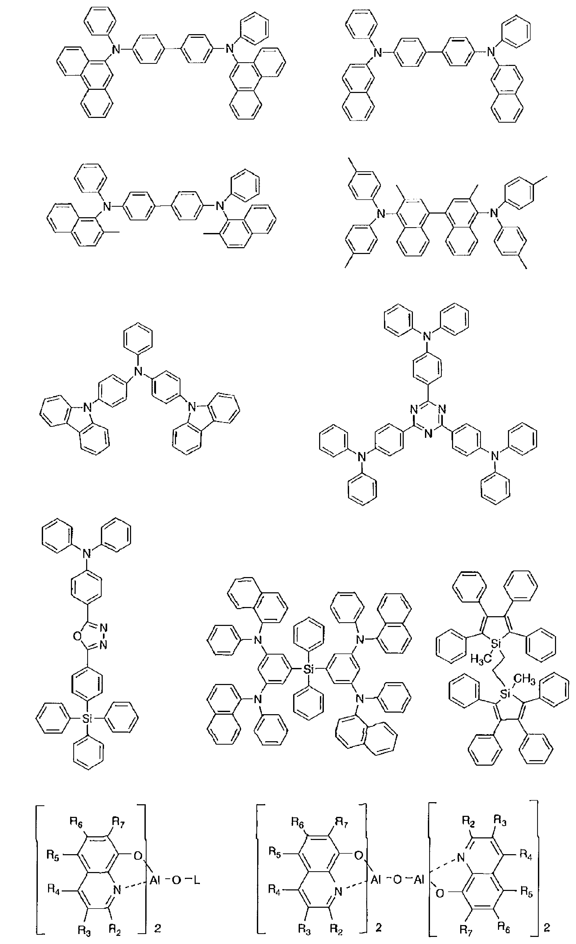

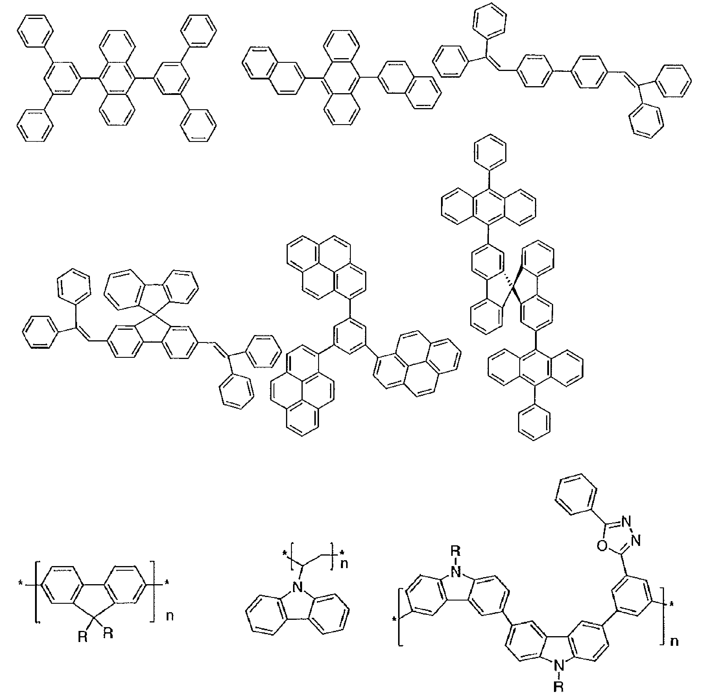
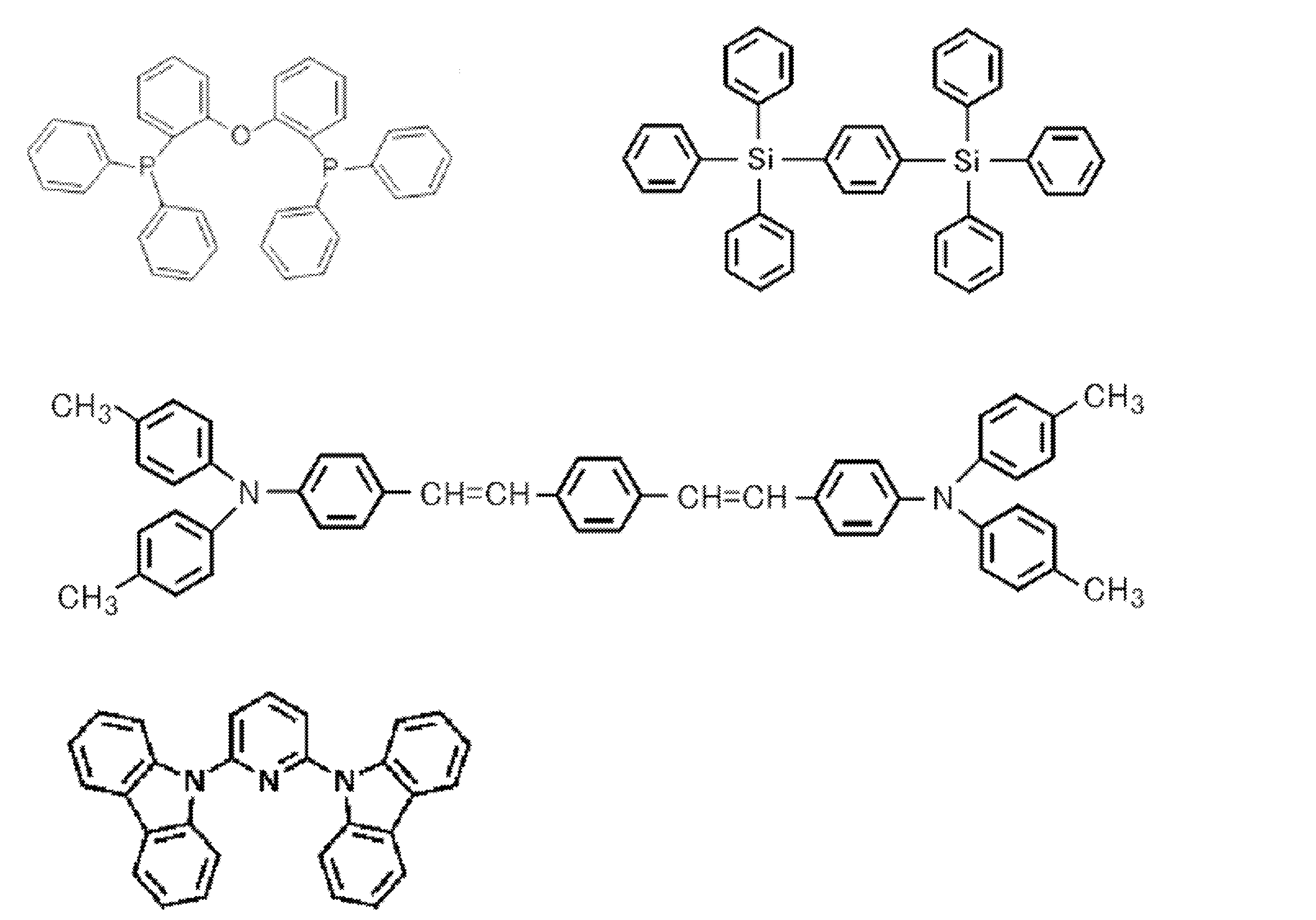
次に、正孔注入材料として用いることができる好ましい化合物例を挙げる。

次に、正孔輸送材料として用いることができる好ましい化合物例を挙げる。
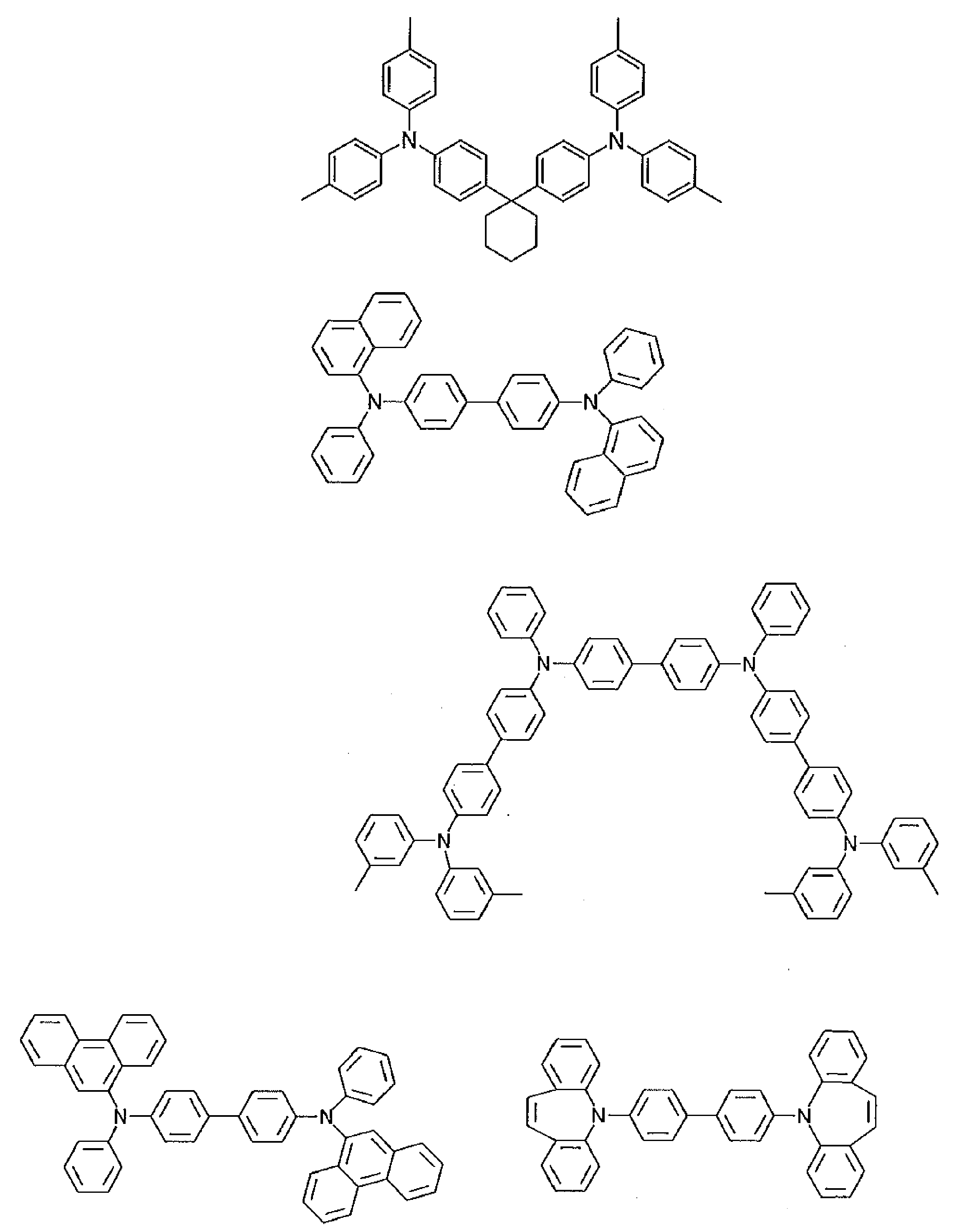

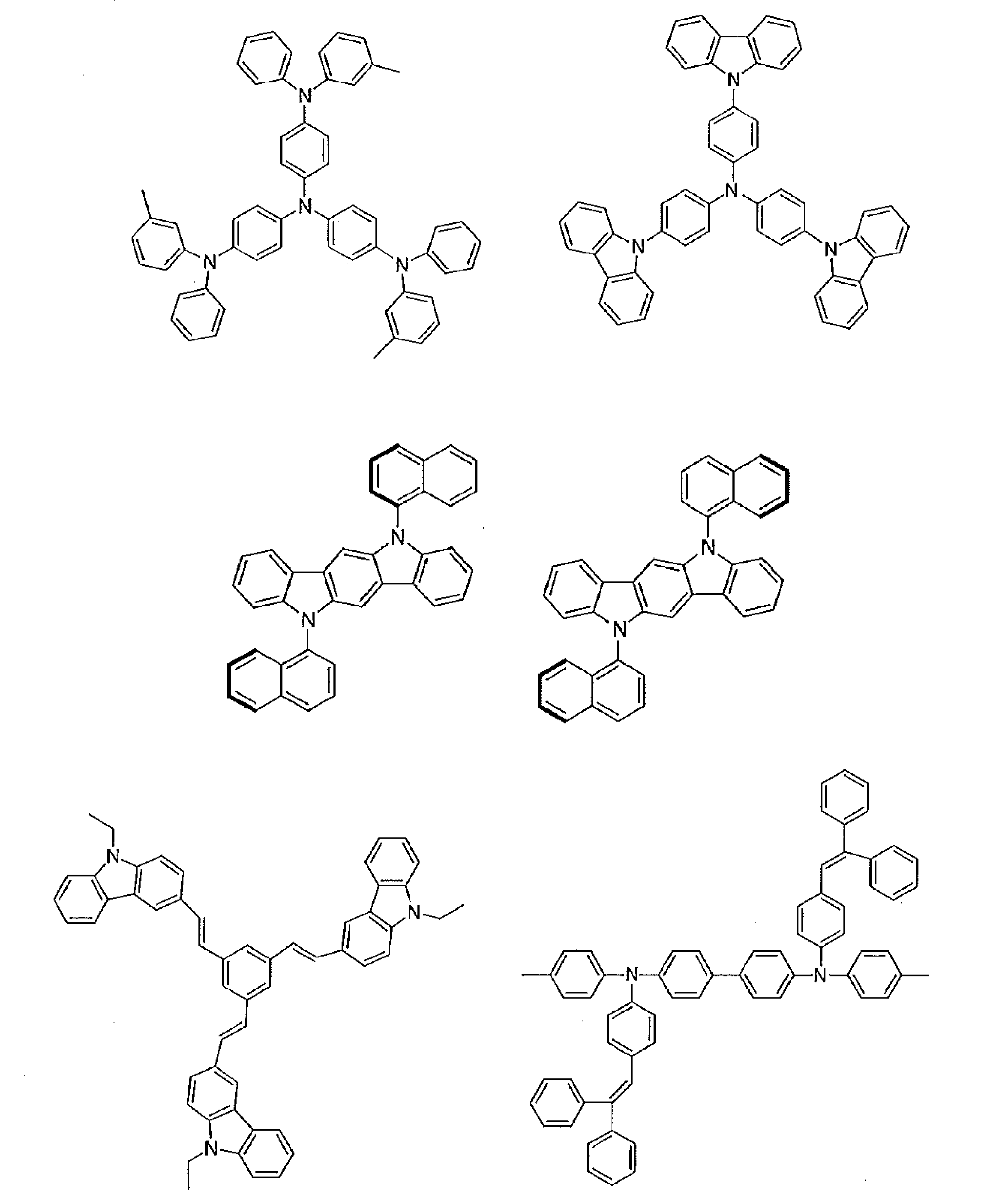


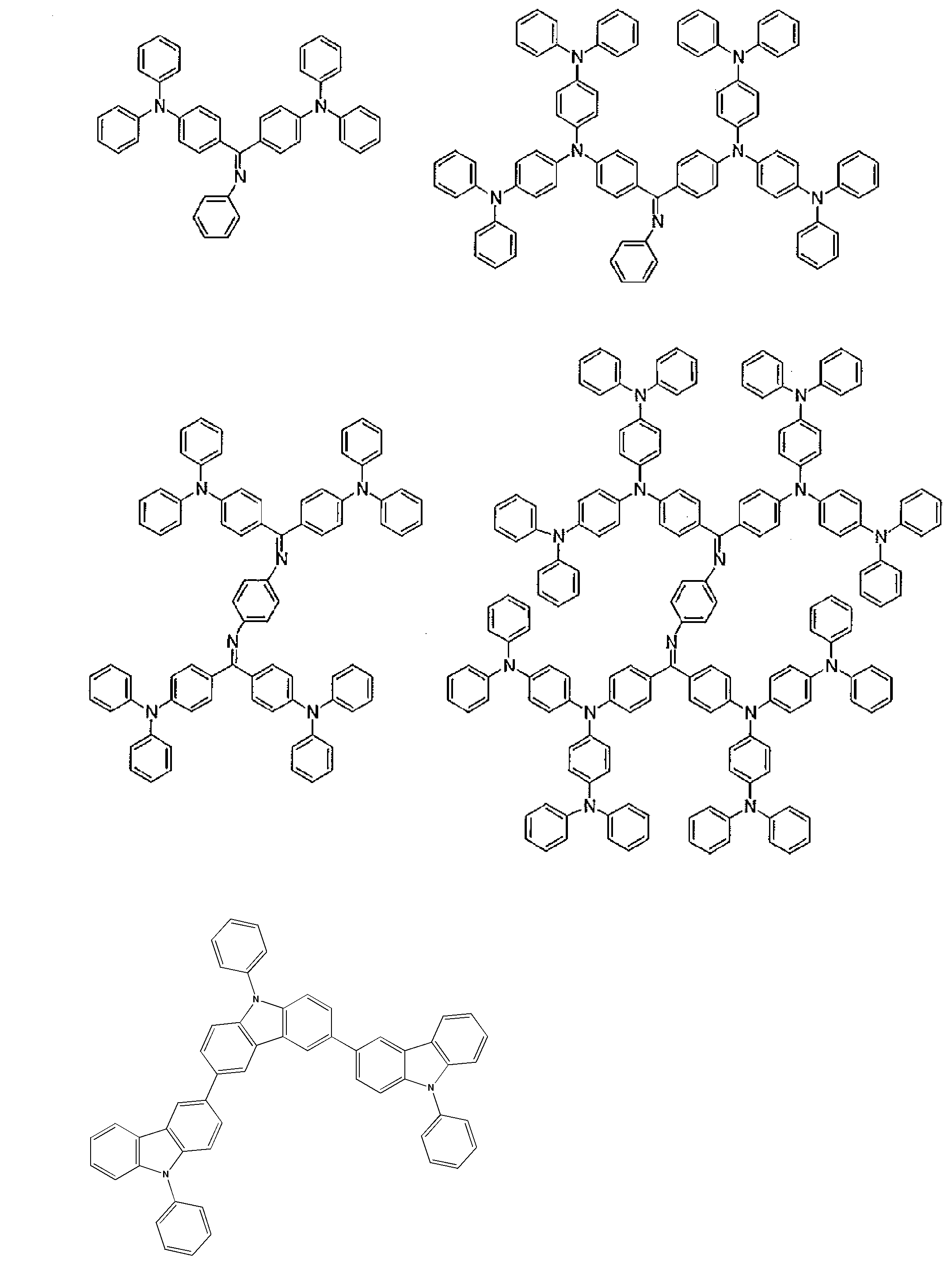
次に、電子阻止材料として用いることができる好ましい化合物例を挙げる。

次に、正孔阻止材料として用いることができる好ましい化合物例を挙げる。
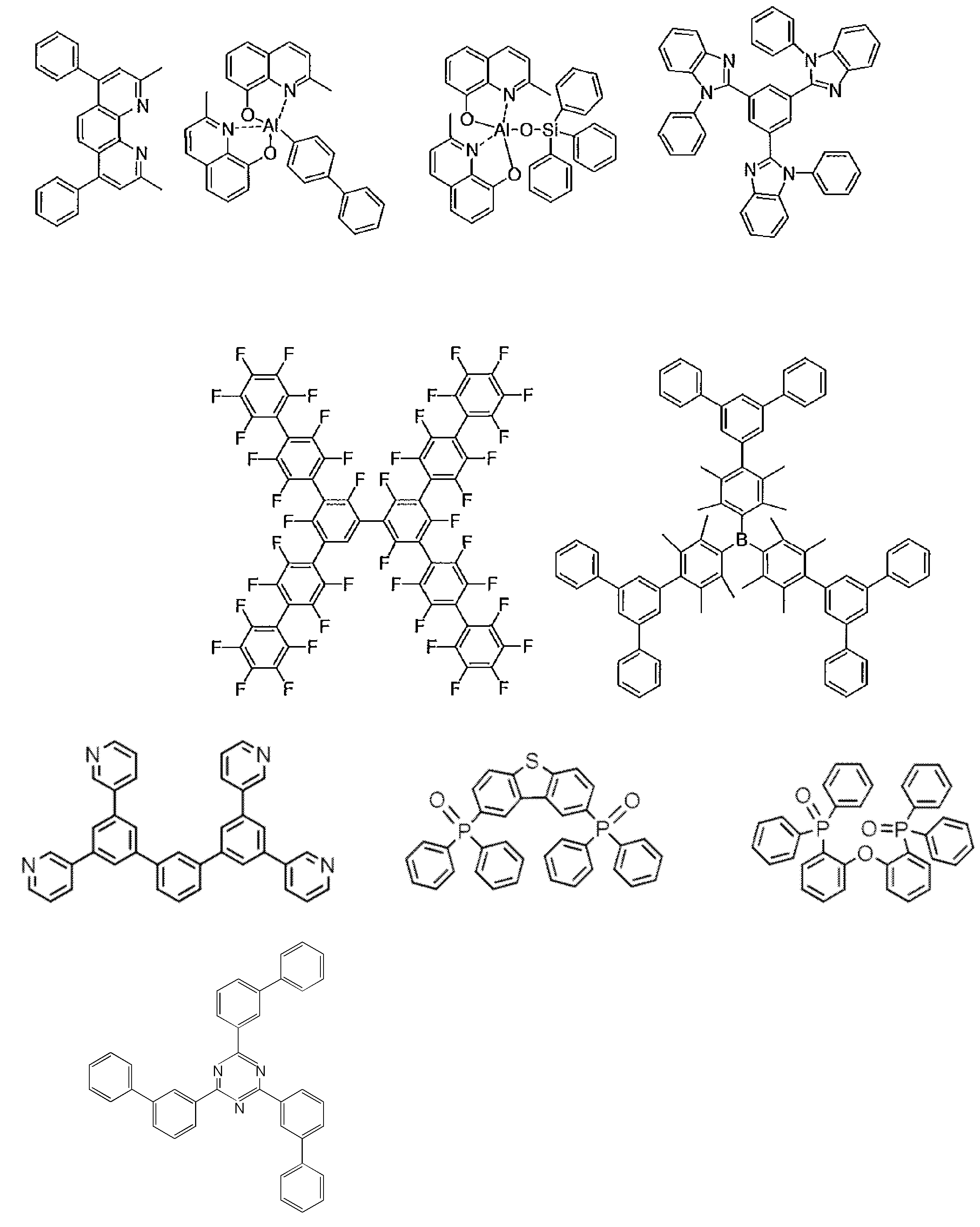
次に、電子輸送材料として用いることができる好ましい化合物例を挙げる。


次に、電子注入材料として用いることができる好ましい化合物例を挙げる。

さらに添加可能な材料として好ましい化合物例を挙げる。例えば、安定化材料として添加すること等が考えられる。
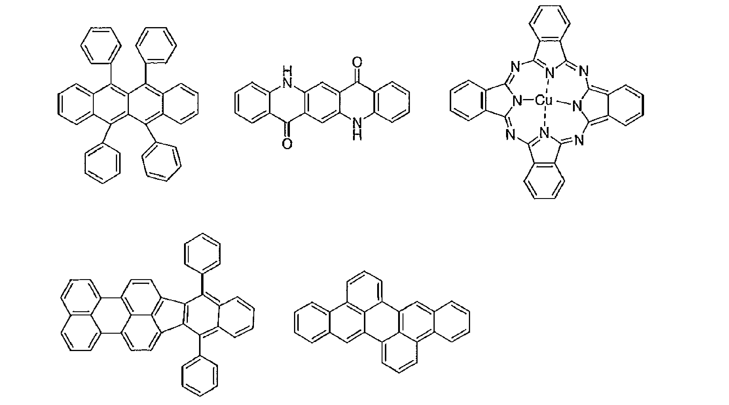
上述の方法により作製された有機エレクトロルミネッセンス素子は、得られた素子の陽極と陰極の間に電界を印加することにより発光する。このとき、励起一重項エネルギーによる発光であれば、そのエネルギーレベルに応じた波長の光が、蛍光発光および遅延蛍光発光として確認される。また、励起三重項エネルギーによる発光であれば、そのエネルギーレベルに応じた波長が、燐光として確認される。通常の蛍光は、遅延蛍光発光よりも蛍光寿命が短いため、発光寿命は蛍光と遅延蛍光で区別できる。
一方、燐光については、通常の有機化合物では、励起三重項エネルギーは不安定で熱等に変換され、寿命が短く直ちに失活するため、室温では殆ど観測できない。通常の有機化合物の励起三重項エネルギーを測定するためには、極低温の条件での発光を観測することにより測定可能である。
一方、燐光については、通常の有機化合物では、励起三重項エネルギーは不安定で熱等に変換され、寿命が短く直ちに失活するため、室温では殆ど観測できない。通常の有機化合物の励起三重項エネルギーを測定するためには、極低温の条件での発光を観測することにより測定可能である。
本発明の有機エレクトロルミネッセンス素子は、単一の素子、アレイ状に配置された構造からなる素子、陽極と陰極がX-Yマトリックス状に配置された構造のいずれにおいても適用することができる。本発明によれば、一般式(1)で表される化合物をホストまたはアシストドーパントとして発光層に含有させることにより、発光効率が大きく改善された有機発光素子が得られる。本発明の有機エレクトロルミネッセンス素子などの有機発光素子は、さらに様々な用途へ応用することが可能である。例えば、本発明の有機エレクトロルミネッセンス素子を用いて、有機エレクトロルミネッセンス表示装置を製造することが可能であり、詳細については、時任静士、安達千波矢、村田英幸共著「有機ELディスプレイ」(オーム社)を参照することができる。また、特に本発明の有機エレクトロルミネッセンス素子は、需要が大きい有機エレクトロルミネッセンス照明やバックライトに応用することもできる。
以下に実施例を挙げて本発明の特徴をさらに具体的に説明する。以下に示す材料、処理内容、処理手順等は、本発明の趣旨を逸脱しない限り適宜変更することができる。したがって、本発明の範囲は以下に示す具体例により限定的に解釈されるべきものではない。なお、発光特性の評価は、ハイパフォーマンス紫外可視近赤外分光光度計(パーキンエルマー社製:Lambda950)、蛍光分光光度計(堀場製作所社製:FluoroMax-4)、絶対PL量子収率測定装置(浜松ホトニクス社製:C11347)、ソースメータ(ケースレー社製:2400シリーズ)、半導体パラメータ・アナライザ(アジレント・テクノロジー社製:E5273A)、光パワーメータ測定装置(ニューポート社製:1930C)、光学分光器(オーシャンオプティクス社製:USB2000)、分光放射計(トプコン社製:SR-3)およびストリークカメラ(浜松ホトニクス(株)製C4334型)を用いて行った。
実施例および比較例で用いた化合物の最低励起一重項エネルギー準位ES1と、最低励起三重項エネルギー準位ET1は、以下の手順により求めた。また、最低励起一重項状態と77Kの最低励起三重項状態とのエネルギーの差ΔEstは、ES1とET1の差を計算することにより求めた。
(1)最低励起一重項エネルギー準位ES1
測定対象化合物をSi基板上に蒸着して試料を作製し、常温(300K)でこの試料の蛍光スペクトルを測定した。蛍光スペクトルは、縦軸を発光、横軸を波長とした。この発光スペクトルの短波側の立ち下がりに対して接線を引き、その接線と横軸との交点の波長値 λedge[nm]を求めた。この波長値を次に示す換算式でエネルギー値に換算した値をES1とした。
換算式:ES1[eV]=1239.85/λedge
発光スペクトルの測定には、励起光源に窒素レーザー(Lasertechnik Berlin社製、MNL200)を検出器には、ストリークカメラ(浜松ホトニクス社製、C4334)を用いた。
(1)最低励起一重項エネルギー準位ES1
測定対象化合物をSi基板上に蒸着して試料を作製し、常温(300K)でこの試料の蛍光スペクトルを測定した。蛍光スペクトルは、縦軸を発光、横軸を波長とした。この発光スペクトルの短波側の立ち下がりに対して接線を引き、その接線と横軸との交点の波長値 λedge[nm]を求めた。この波長値を次に示す換算式でエネルギー値に換算した値をES1とした。
換算式:ES1[eV]=1239.85/λedge
発光スペクトルの測定には、励起光源に窒素レーザー(Lasertechnik Berlin社製、MNL200)を検出器には、ストリークカメラ(浜松ホトニクス社製、C4334)を用いた。
(2)最低励起三重項エネルギー準位ET1
一重項エネルギーES1と同じ試料を77[K]に冷却し、励起光(337nm)を燐光測定用試料に照射し、ストリークカメラを用いて、燐光強度を測定した。この燐光スペクトルの短波長側の立ち上がりに対して接線を引き、その接線と横軸との交点の波長値λedge[nm]を求めた。この波長値を次に示す換算式でエネルギー値に換算した値をET1とした。
換算式:ET1[eV]=1239.85/λedge
燐光スペクトルの短波長側の立ち上がりに対する接線は以下のように引いた。燐光スペクトルの短波長側から、スペクトルの極大値のうち、最も短波長側の極大値までスペクトル曲線上を移動する際に、長波長側に向けて曲線上の各点における接線を考える。この接線は、曲線が立ち上がるにつれ(つまり縦軸が増加するにつれ)、傾きが増加する。この傾きの値が極大値をとる点において引いた接線を、当該燐光スペクトルの短波長側の立ち上がりに対する接線とした。
なお、スペクトルの最大ピーク強度の10%以下のピーク強度をもつ極大点は、上述の最も短波長側の極大値には含めず、最も短波長側の極大値に最も近い、傾きの値が極大値をとる点において引いた接線を当該燐光スペクトルの短波長側の立ち上がりに対する接線とした。
一重項エネルギーES1と同じ試料を77[K]に冷却し、励起光(337nm)を燐光測定用試料に照射し、ストリークカメラを用いて、燐光強度を測定した。この燐光スペクトルの短波長側の立ち上がりに対して接線を引き、その接線と横軸との交点の波長値λedge[nm]を求めた。この波長値を次に示す換算式でエネルギー値に換算した値をET1とした。
換算式:ET1[eV]=1239.85/λedge
燐光スペクトルの短波長側の立ち上がりに対する接線は以下のように引いた。燐光スペクトルの短波長側から、スペクトルの極大値のうち、最も短波長側の極大値までスペクトル曲線上を移動する際に、長波長側に向けて曲線上の各点における接線を考える。この接線は、曲線が立ち上がるにつれ(つまり縦軸が増加するにつれ)、傾きが増加する。この傾きの値が極大値をとる点において引いた接線を、当該燐光スペクトルの短波長側の立ち上がりに対する接線とした。
なお、スペクトルの最大ピーク強度の10%以下のピーク強度をもつ極大点は、上述の最も短波長側の極大値には含めず、最も短波長側の極大値に最も近い、傾きの値が極大値をとる点において引いた接線を当該燐光スペクトルの短波長側の立ち上がりに対する接線とした。
(合成例1) 化合物1の合成
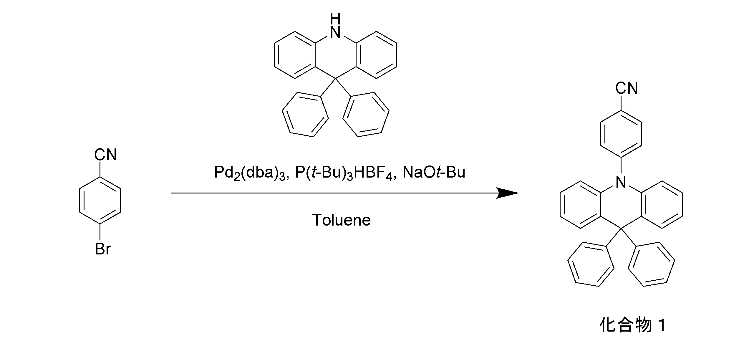
4-ブロモベンゾニトリル(0.5g,2.75mmol)、9,9-ジフェニルアクリジン(0.99g,3.0mmol)、トリス(ジベンジリデンアセトン)ジパラジウム(0.76g,0.825mmol)、トリ-tert-ブチルホスホニウムテトラフルオロボラート(0.96g,3.3mmol)、ナトリウムtert-ブトキシド(0.53g,5.5mmol)を100mlの容器に加え、三度窒素置換を行った。その後、トルエン30mlを加え、24時間110℃加熱撹拌した。この反応液を室温に冷却した後、トルエンで希釈しセライト濾過を行い、濃縮した。この濃縮物を、ジクロロメタン:ヘキサン=2:3の混合溶媒を展開溶媒に用いるシリカゲルクロマトグラフィーによって精製し、白色粉末である4-(10H-9,9-ジフェニルアクリジン-10-イル)ベンゾニトリルを収量0.987g、収率83%で得た。
(合成例2) 化合物2の合成
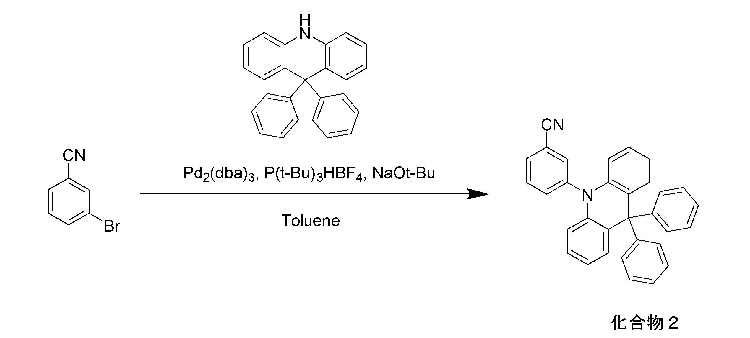
4-ブロモベンゾニトリルを3-ブロモベンゾニトリル(0.5g,2.75mmol)に変更したこと以外は、合成例1と同様の操作を行うことにより、白色粉末である3-(10H-9,9-ジフェニルアクリジン-10-イル)ベンゾニトリルを収量0.861g、収率72%で得た。
(合成例3) 化合物3の合成
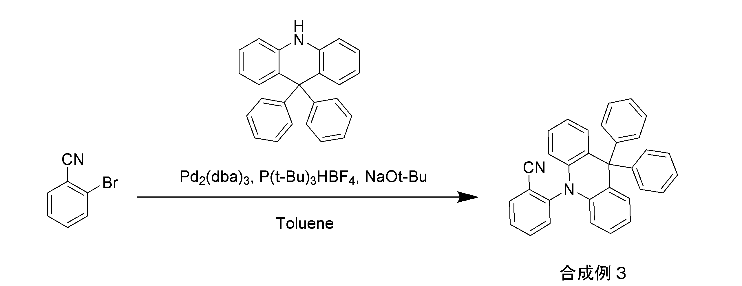
4-ブロモベンゾニトリルを2-ブロモベンゾニトリル(0.5g,2.75mmol)に変更したこと以外は、合成例1と同様の操作を行うことにより、白色粉末である2-(10H-9,9-ジフェニルアクリジン-10-イル)ベンゾニトリルを収量1.022g、収率86%で得た。
(合成例4) 化合物4の合成
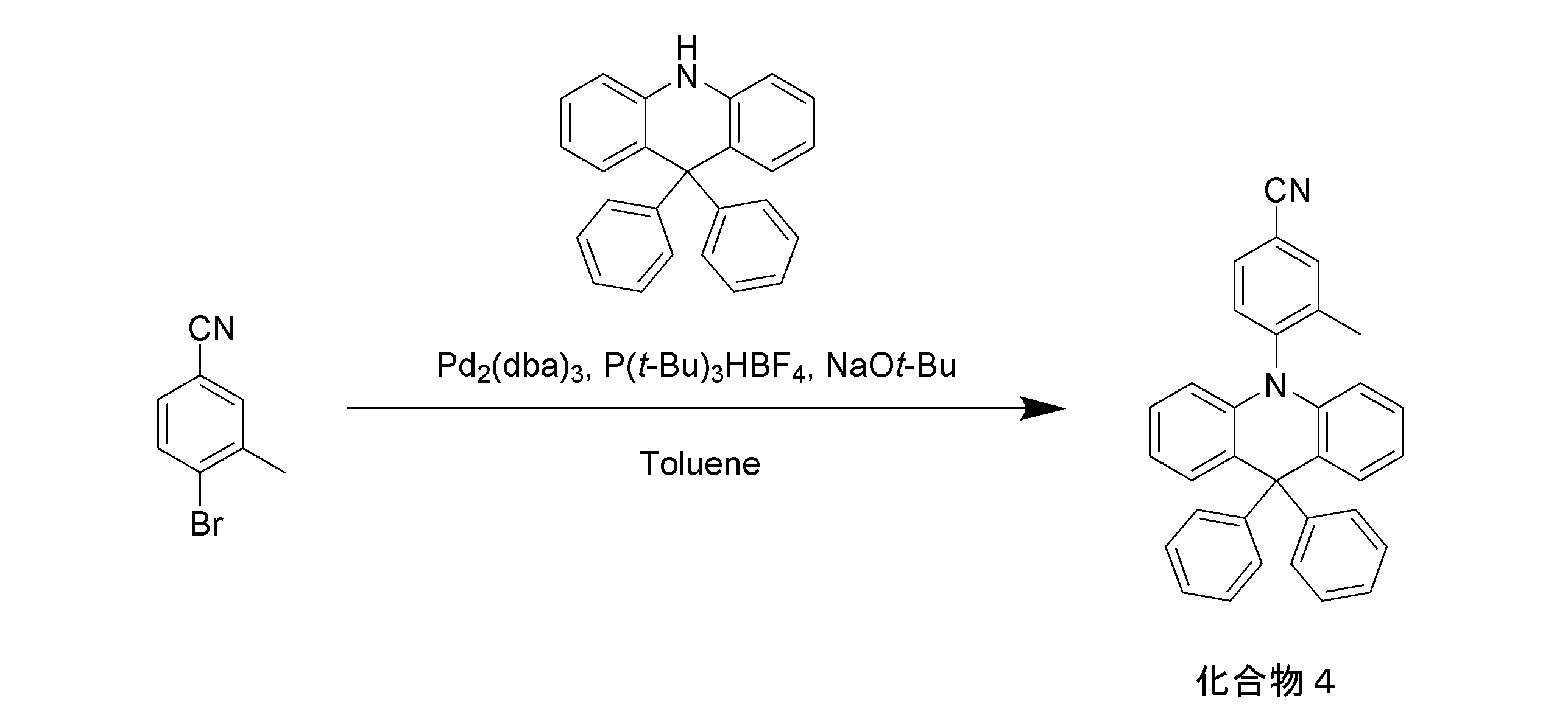
4-ブロモベンゾニトリルを4-ブロモ-3-メチルベンゾニトリル(0.5g,2.55mmol)に変更し、9,9-ジフェニルアクリジンの使用量を0.99g(3.0mmol)から0.93g(2.8mmol)に変更したこと以外は、合成例1と同様の操作を行うことにより、白色粉末である3-メチル-4-(10H-9,9-ジフェニルアクリジン-10-イル)ベンゾニトリルを収量0.89g、収率78%で得た。
(合成例5) 化合物5の合成
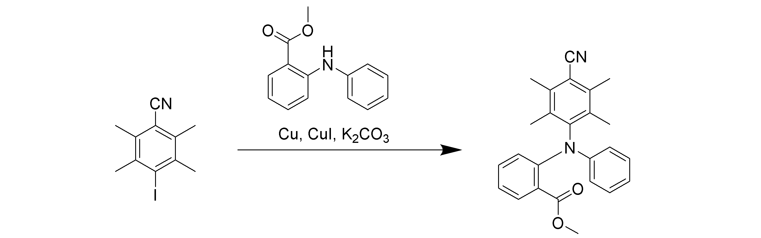
4-ヨード-2,3,5,6-テトラメチルベンゾニトリル(2g,7.0mmol)、2-(フェニルアミノ)安息香酸メチル(1.9g,8.4mmol)、銅粉末(0.94g,7mmol)、ヨウ化銅(1.3g,7mmol)、炭酸カリウム(1.06g,7.7mmol)を100mlの三口フラスコに加え、三度窒素置換を行った。その後、無溶媒で24時間190℃加熱撹拌した。この反応液を室温に冷却した後、ジクロロメタンで希釈しセライト濾過を行い、濃縮した。この濃縮物を、ジクロロメタン:ヘキサン=1:4の混合溶媒を展開溶媒に用いるシリカゲルクロマトグラフィーによって精製し、黄色粉末であるN-(4-シアノ-2,3,5,6-テトラメチルフェニル)-N-フェニルアントラニル酸メチルを収量1.978g、収率73%で得た。

(合成例6) 化合物6の合成
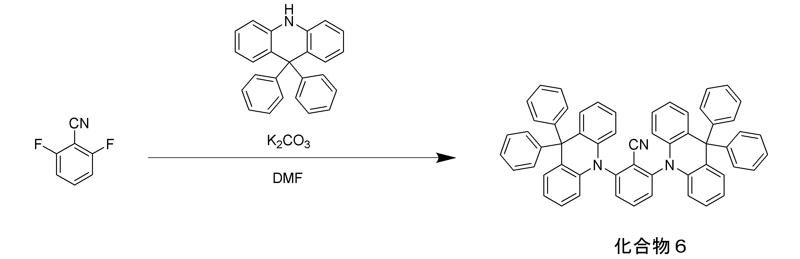
2,6-ジフルオロベンゾニトリル(0.2g,1.44mmol)、9,9-ジフェニルアクリジン(0.99g,3.0mmol)、炭酸カリウム(0.5g,3.6mmol)を100mlの容器に加え、三度窒素置換した。その後、ジメチルホルムアミド25ml加え、三日間153℃加熱撹拌した。反応溶液を室温に冷却した後、水で洗浄しジクロロメタンで抽出し、濃縮した。この濃縮物を、ジクロロメタン:ヘキサン=1:4の混合溶媒を展開溶媒に用いるシリカゲルクロマトグラフィーによって精製し、白色粉末である2,5-ビス(10H-9,9-ジフェニルアクリジン-10-イル)ベンゾニトリルを収量0.413g、収率38%で得た。
以上のようにして合成された化合物1~6の特性値を表1に示す。
なお、HOMOは大気中光電子分光法で測定することにより決定した値であり、LUMOは吸収スペクトル端によって求めたエネルギーギャップを使用することにより決定した値である。
以上のようにして合成された化合物1~6の特性値を表1に示す。
なお、HOMOは大気中光電子分光法で測定することにより決定した値であり、LUMOは吸収スペクトル端によって求めたエネルギーギャップを使用することにより決定した値である。
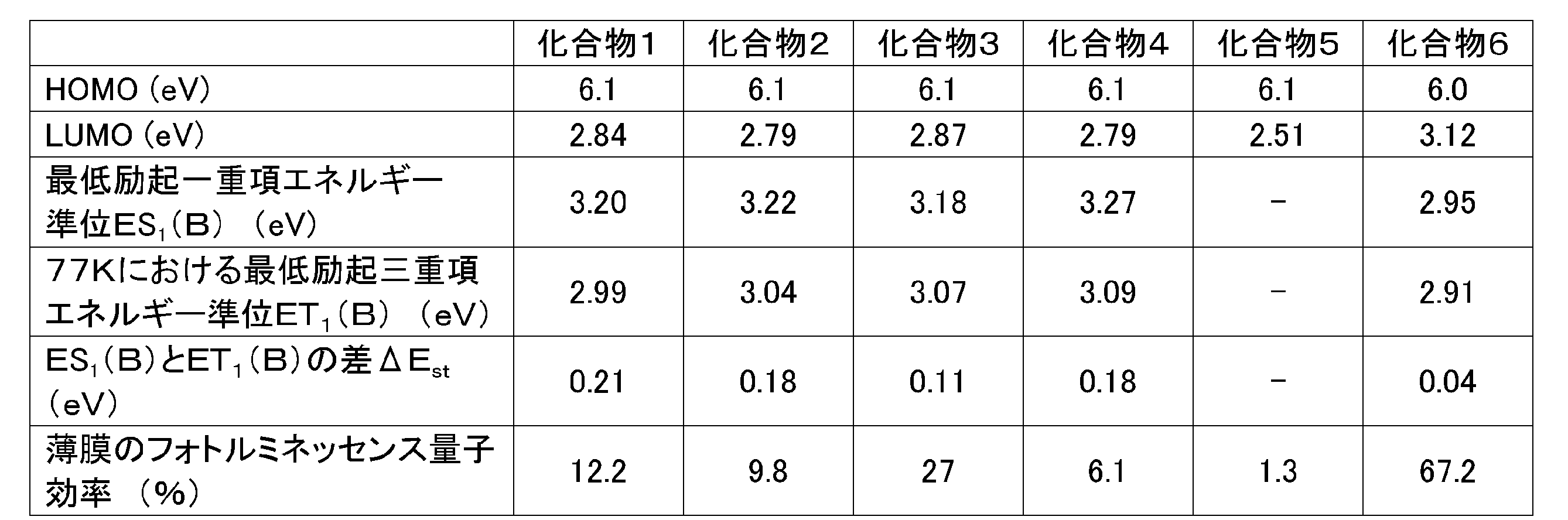
(試験例1) 化合物1の溶液と薄膜の作製と評価
Ar雰囲気のグローブボックス中で化合物1のトルエン溶液(濃度10-4~10-5mol/L)を調製した。
また、石英基板上に真空蒸着法にて真空度5×10⁻⁴Pa以下で化合物1の薄膜を100nmの厚さで形成した。
化合物1のトルエン溶液について、353nm励起光による吸収発光スペクトルを測定した結果を図2に示す。
フォトルミネッセンス量子効率は、窒素でバブリングする前のトルエン溶液で24%、窒素でバブリングしたトルエン溶液で29%であった。
化合物1のトルエン溶液について、過渡減衰曲線を測定した結果を図3に示す。また、化合物1の薄膜について、300K、5Kの各温度で測定した337nm励起光による過渡減衰曲線を図4に示す。図4より、温度上昇に伴って遅延蛍光成分が増加する熱活性型の遅延蛍光であることが確認された。また、化合物1の薄膜のフォトルミネッセンス量子効率は12.2%であった。
化合物1の薄膜について、300K、5Kの各温度で測定した即時発光スペクトル(Prompt)および遅延発光スペクトル(Delay)を図5に示す。ここでは、過渡減衰曲線に対して二次関数でフィッティングした際に速い成分を即時発光スペクトル(Prompt)とし、遅い成分を遅延発光スペクトル(Delay)とした。図5において、300Kにおける即時発光スペクトルは蛍光スペクトルに対応し、300Kにおける遅延発光スペクトルは遅延蛍光スペクトルに対応する。また、5Kにおける即時発光スペクトルは蛍光スペクトルに対応し、遅延発光スペクトルは燐光スペクトルに対応する。
Ar雰囲気のグローブボックス中で化合物1のトルエン溶液(濃度10-4~10-5mol/L)を調製した。
また、石英基板上に真空蒸着法にて真空度5×10⁻⁴Pa以下で化合物1の薄膜を100nmの厚さで形成した。
化合物1のトルエン溶液について、353nm励起光による吸収発光スペクトルを測定した結果を図2に示す。
フォトルミネッセンス量子効率は、窒素でバブリングする前のトルエン溶液で24%、窒素でバブリングしたトルエン溶液で29%であった。
化合物1のトルエン溶液について、過渡減衰曲線を測定した結果を図3に示す。また、化合物1の薄膜について、300K、5Kの各温度で測定した337nm励起光による過渡減衰曲線を図4に示す。図4より、温度上昇に伴って遅延蛍光成分が増加する熱活性型の遅延蛍光であることが確認された。また、化合物1の薄膜のフォトルミネッセンス量子効率は12.2%であった。
化合物1の薄膜について、300K、5Kの各温度で測定した即時発光スペクトル(Prompt)および遅延発光スペクトル(Delay)を図5に示す。ここでは、過渡減衰曲線に対して二次関数でフィッティングした際に速い成分を即時発光スペクトル(Prompt)とし、遅い成分を遅延発光スペクトル(Delay)とした。図5において、300Kにおける即時発光スペクトルは蛍光スペクトルに対応し、300Kにおける遅延発光スペクトルは遅延蛍光スペクトルに対応する。また、5Kにおける即時発光スペクトルは蛍光スペクトルに対応し、遅延発光スペクトルは燐光スペクトルに対応する。
(試験例2) 化合物2の溶液と薄膜の作製と評価
化合物1のかわりに化合物2を用いた点を変更して、実施例1と同じ条件で化合物2のトルエン溶液と化合物2の薄膜を作製した。
化合物2のトルエン溶液について、340nm励起光による吸収発光スペクトルを測定した結果を図6に示す。
フォトルミネッセンス量子効率は、窒素でバブリングする前のトルエン溶液で4%、窒素でバブリングしたトルエン溶液で10%であった。
化合物2のトルエン溶液について、過渡減衰曲線を測定した結果を図7に示す。また、化合物2の薄膜について、300K、200K、100K、5Kの各温度で測定した337nm励起光による過渡減衰曲線を図8に示す。図8より、温度上昇に伴って遅延蛍光成分が増加する熱活性型の遅延蛍光であることが確認された。また、化合物2の薄膜のフォトルミネッセンス量子効率は9.8%であった。
化合物2の薄膜について、300K、5Kの各温度で測定した即時発光スペクトル(Prompt)および遅延発光スペクトル(Delay)を図9に示す。図9において、300Kにおける即時発光スペクトルは蛍光スペクトルに対応し、300Kにおける遅延発光スペクトルは遅延蛍光スペクトルに対応する。また、5Kにおける即時発光スペクトルは蛍光スペクトルに対応し、遅延発光スペクトルは燐光スペクトルに対応する。
化合物1のかわりに化合物2を用いた点を変更して、実施例1と同じ条件で化合物2のトルエン溶液と化合物2の薄膜を作製した。
化合物2のトルエン溶液について、340nm励起光による吸収発光スペクトルを測定した結果を図6に示す。
フォトルミネッセンス量子効率は、窒素でバブリングする前のトルエン溶液で4%、窒素でバブリングしたトルエン溶液で10%であった。
化合物2のトルエン溶液について、過渡減衰曲線を測定した結果を図7に示す。また、化合物2の薄膜について、300K、200K、100K、5Kの各温度で測定した337nm励起光による過渡減衰曲線を図8に示す。図8より、温度上昇に伴って遅延蛍光成分が増加する熱活性型の遅延蛍光であることが確認された。また、化合物2の薄膜のフォトルミネッセンス量子効率は9.8%であった。
化合物2の薄膜について、300K、5Kの各温度で測定した即時発光スペクトル(Prompt)および遅延発光スペクトル(Delay)を図9に示す。図9において、300Kにおける即時発光スペクトルは蛍光スペクトルに対応し、300Kにおける遅延発光スペクトルは遅延蛍光スペクトルに対応する。また、5Kにおける即時発光スペクトルは蛍光スペクトルに対応し、遅延発光スペクトルは燐光スペクトルに対応する。
(試験例3) 化合物3の溶液と薄膜の作製と評価
化合物1のかわりに化合物3を用いた点を変更して、実施例1と同じ条件で化合物3のトルエン溶液と化合物3の薄膜を作製した。
化合物3のトルエン溶液について、340nm励起光による吸収発光スペクトルを測定した結果を図10に示す。
フォトルミネッセンス量子効率は、窒素でバブリングする前のトルエン溶液で5.5%、窒素でバブリングしたトルエン溶液で33%であった。
化合物3のトルエン溶液について、過渡減衰曲線を測定した結果を図11に示す。また、化合物3の薄膜について、300K、200K、100K、5Kの各温度で測定した337nm励起光による過渡減衰曲線を図12に示す。図12より、温度上昇に伴って遅延蛍光成分が増加する熱活性型の遅延蛍光であることが確認された。また、化合物3の薄膜のフォトルミネッセンス量子効率は27%であった。
化合物3の薄膜について、5Kで測定した即時発光スペクトル(Prompt)および遅延発光スペクトル(Delay)を図13に示す。図13において、即時発光スペクトルは蛍光スペクトルに対応し、遅延発光スペクトルは燐光スペクトルに対応する。化合物3の最低励起一重項状態でのエネルギー準位Es1は3.18eVであり、最低励起三重項状態でのエネルギー準位ET1は3.07eVであり、差ΔEstは0.11eVであった。
化合物1のかわりに化合物3を用いた点を変更して、実施例1と同じ条件で化合物3のトルエン溶液と化合物3の薄膜を作製した。
化合物3のトルエン溶液について、340nm励起光による吸収発光スペクトルを測定した結果を図10に示す。
フォトルミネッセンス量子効率は、窒素でバブリングする前のトルエン溶液で5.5%、窒素でバブリングしたトルエン溶液で33%であった。
化合物3のトルエン溶液について、過渡減衰曲線を測定した結果を図11に示す。また、化合物3の薄膜について、300K、200K、100K、5Kの各温度で測定した337nm励起光による過渡減衰曲線を図12に示す。図12より、温度上昇に伴って遅延蛍光成分が増加する熱活性型の遅延蛍光であることが確認された。また、化合物3の薄膜のフォトルミネッセンス量子効率は27%であった。
化合物3の薄膜について、5Kで測定した即時発光スペクトル(Prompt)および遅延発光スペクトル(Delay)を図13に示す。図13において、即時発光スペクトルは蛍光スペクトルに対応し、遅延発光スペクトルは燐光スペクトルに対応する。化合物3の最低励起一重項状態でのエネルギー準位Es1は3.18eVであり、最低励起三重項状態でのエネルギー準位ET1は3.07eVであり、差ΔEstは0.11eVであった。
(試験例4) 化合物4の溶液と薄膜の作製と評価
化合物1のかわりに化合物4を用いた点を変更して、実施例1と同じ条件で化合物4のトルエン溶液と化合物4の薄膜を作製した。
化合物4のトルエン溶液について、340nm励起光による吸収発光スペクトルを測定した結果を図14に示す。
フォトルミネッセンス量子効率は、窒素でバブリングする前のトルエン溶液で4%、窒素でバブリングしたトルエン溶液で7%であった。
化合物4のトルエン溶液について、過渡減衰曲線を測定した結果を図15に示す。また、化合物4の薄膜について、300K、200K、100K、5Kの各温度で測定した337nm励起光による過渡減衰曲線を図16に示す。図16より、温度上昇に伴って遅延蛍光成分が増加する熱活性型の遅延蛍光であることが確認された。また、化合物4の薄膜のフォトルミネッセンス量子効率は6.1%であった。
化合物4の薄膜について、5Kで測定した即時発光スペクトル(Prompt)および遅延発光スペクトル(Delay)を図17に示す。図17において、即時発光スペクトルは蛍光スペクトルに対応し、遅延発光スペクトルは燐光スペクトルに対応する。化合物4の最低励起一重項状態でのエネルギー準位Es1と最低励起三重項状態でのエネルギー準位ET1の差ΔEstは0.18eVであった。
化合物1のかわりに化合物4を用いた点を変更して、実施例1と同じ条件で化合物4のトルエン溶液と化合物4の薄膜を作製した。
化合物4のトルエン溶液について、340nm励起光による吸収発光スペクトルを測定した結果を図14に示す。
フォトルミネッセンス量子効率は、窒素でバブリングする前のトルエン溶液で4%、窒素でバブリングしたトルエン溶液で7%であった。
化合物4のトルエン溶液について、過渡減衰曲線を測定した結果を図15に示す。また、化合物4の薄膜について、300K、200K、100K、5Kの各温度で測定した337nm励起光による過渡減衰曲線を図16に示す。図16より、温度上昇に伴って遅延蛍光成分が増加する熱活性型の遅延蛍光であることが確認された。また、化合物4の薄膜のフォトルミネッセンス量子効率は6.1%であった。
化合物4の薄膜について、5Kで測定した即時発光スペクトル(Prompt)および遅延発光スペクトル(Delay)を図17に示す。図17において、即時発光スペクトルは蛍光スペクトルに対応し、遅延発光スペクトルは燐光スペクトルに対応する。化合物4の最低励起一重項状態でのエネルギー準位Es1と最低励起三重項状態でのエネルギー準位ET1の差ΔEstは0.18eVであった。
(試験例5)化合物5の溶液の調製と評価
化合物1のかわりに化合物5を用いた点を変更して、実施例1と同じ条件で化合物5のトルエン溶液を調製した。
化合物5のトルエン溶液について、322nm励起光による吸収発光スペクトルを測定した結果を図18に示す。
フォトルミネッセンス量子効率は、窒素でバブリングする前のトルエン溶液で1%、窒素でバブリングしたトルエン溶液で2%であった。
化合物5のトルエン溶液について、過渡減衰曲線を測定した結果を図19に示す。図19を見ると、窒素バブリング後の方が窒素バブリング前よりも発光寿命が延長しており、低酸素濃度の条件下で発光強度が大きくなる遅延蛍光の特徴を観測することができた。
化合物1のかわりに化合物5を用いた点を変更して、実施例1と同じ条件で化合物5のトルエン溶液を調製した。
化合物5のトルエン溶液について、322nm励起光による吸収発光スペクトルを測定した結果を図18に示す。
フォトルミネッセンス量子効率は、窒素でバブリングする前のトルエン溶液で1%、窒素でバブリングしたトルエン溶液で2%であった。
化合物5のトルエン溶液について、過渡減衰曲線を測定した結果を図19に示す。図19を見ると、窒素バブリング後の方が窒素バブリング前よりも発光寿命が延長しており、低酸素濃度の条件下で発光強度が大きくなる遅延蛍光の特徴を観測することができた。
(試験例6)化合物6の溶液の調製と評価
化合物1のかわりに化合物6を用いた点を変更して、実施例1と同じ条件で化合物6のトルエン溶液を調製した。
化合物6のトルエン溶液について、360nm励起光による吸収発光スペクトルを測定した結果を図20に示す。
フォトルミネッセンス量子効率は、空気でバブリングしたトルエン溶液で6.7%、窒素でバブリングしたトルエン溶液で64%であった。
化合物6のトルエン溶液について、過渡減衰曲線を測定した結果を図21に示す。また、化合物6の薄膜について、300K、200K、100K、8Kの各温度で測定した337nm励起光による過渡減衰曲線を図22に示す。図22より、温度上昇に伴って遅延蛍光成分が増加する熱活性型の遅延蛍光であることが確認された。また、化合物6の薄膜のフォトルミネッセンス量子効率は67.2%であった。
化合物6の薄膜について、5Kで測定した即時発光スペクトル(Prompt)および遅延発光スペクトル(Delay)を図23に示す。図23において、即時発光スペクトルは蛍光スペクトルに対応し、遅延発光スペクトルは燐光スペクトルに対応する。化合物6の最低励起一重項状態でのエネルギー準位Es1と最低励起三重項状態でのエネルギー準位ET1の差ΔEstは0.04eVであった。
化合物1のかわりに化合物6を用いた点を変更して、実施例1と同じ条件で化合物6のトルエン溶液を調製した。
化合物6のトルエン溶液について、360nm励起光による吸収発光スペクトルを測定した結果を図20に示す。
フォトルミネッセンス量子効率は、空気でバブリングしたトルエン溶液で6.7%、窒素でバブリングしたトルエン溶液で64%であった。
化合物6のトルエン溶液について、過渡減衰曲線を測定した結果を図21に示す。また、化合物6の薄膜について、300K、200K、100K、8Kの各温度で測定した337nm励起光による過渡減衰曲線を図22に示す。図22より、温度上昇に伴って遅延蛍光成分が増加する熱活性型の遅延蛍光であることが確認された。また、化合物6の薄膜のフォトルミネッセンス量子効率は67.2%であった。
化合物6の薄膜について、5Kで測定した即時発光スペクトル(Prompt)および遅延発光スペクトル(Delay)を図23に示す。図23において、即時発光スペクトルは蛍光スペクトルに対応し、遅延発光スペクトルは燐光スペクトルに対応する。化合物6の最低励起一重項状態でのエネルギー準位Es1と最低励起三重項状態でのエネルギー準位ET1の差ΔEstは0.04eVであった。
(実施例1) 化合物2を用いた有機エレクトロルミネッセンス素子の作製と評価
膜厚100nmのインジウム・スズ酸化物(ITO)からなる陽極が形成されたガラス基板上に、各薄膜を真空蒸着法にて、真空度5×10⁻⁴Paで積層した。まず、ITO上にα-NPDを35nmの厚さに形成し、その上にmCPを10nmの厚さに形成した。次に、化合物2とTBPeを異なる蒸着源から共蒸着し、15nmの厚さの層を形成して発光層とした。この時、TBPeの濃度は1.0重量%とした。次に、DPEPOを10nmの厚さに形成し、その上に、TPBiを30nmの厚さに形成した。さらにフッ化リチウム(LiF)を0.8nm真空蒸着し、次いでアルミニウム(Al)を100nmの厚さに蒸着することにより陰極を形成し、有機エレクトロルミネッセンス素子とした。
製造した有機エレクトロルミネッセンス素子の過渡減衰曲線を図24に示し、即時発光スペクトル(Prompt)および遅延発光スペクトル(Delay)を図25に示す。化合物2をホストとして用いた有機エレクトロルミネッセンス素子の外部量子効率は2.8%であった。
また、比較として、石英基板上にTBPeを1重量%ドープした化合物2の薄膜を成膜し、この薄膜について上記の有機エレクトロルミネッセンス素子と同様にして即時発光スペクトル(Prompt)および遅延発光スペクトル(Delay)を測定した。その結果を図26に示す。この化合物2の薄膜のフォトルミネッセンス量子効率(全発光量子収率)は72.2%であった。
膜厚100nmのインジウム・スズ酸化物(ITO)からなる陽極が形成されたガラス基板上に、各薄膜を真空蒸着法にて、真空度5×10⁻⁴Paで積層した。まず、ITO上にα-NPDを35nmの厚さに形成し、その上にmCPを10nmの厚さに形成した。次に、化合物2とTBPeを異なる蒸着源から共蒸着し、15nmの厚さの層を形成して発光層とした。この時、TBPeの濃度は1.0重量%とした。次に、DPEPOを10nmの厚さに形成し、その上に、TPBiを30nmの厚さに形成した。さらにフッ化リチウム(LiF)を0.8nm真空蒸着し、次いでアルミニウム(Al)を100nmの厚さに蒸着することにより陰極を形成し、有機エレクトロルミネッセンス素子とした。
製造した有機エレクトロルミネッセンス素子の過渡減衰曲線を図24に示し、即時発光スペクトル(Prompt)および遅延発光スペクトル(Delay)を図25に示す。化合物2をホストとして用いた有機エレクトロルミネッセンス素子の外部量子効率は2.8%であった。
また、比較として、石英基板上にTBPeを1重量%ドープした化合物2の薄膜を成膜し、この薄膜について上記の有機エレクトロルミネッセンス素子と同様にして即時発光スペクトル(Prompt)および遅延発光スペクトル(Delay)を測定した。その結果を図26に示す。この化合物2の薄膜のフォトルミネッセンス量子効率(全発光量子収率)は72.2%であった。
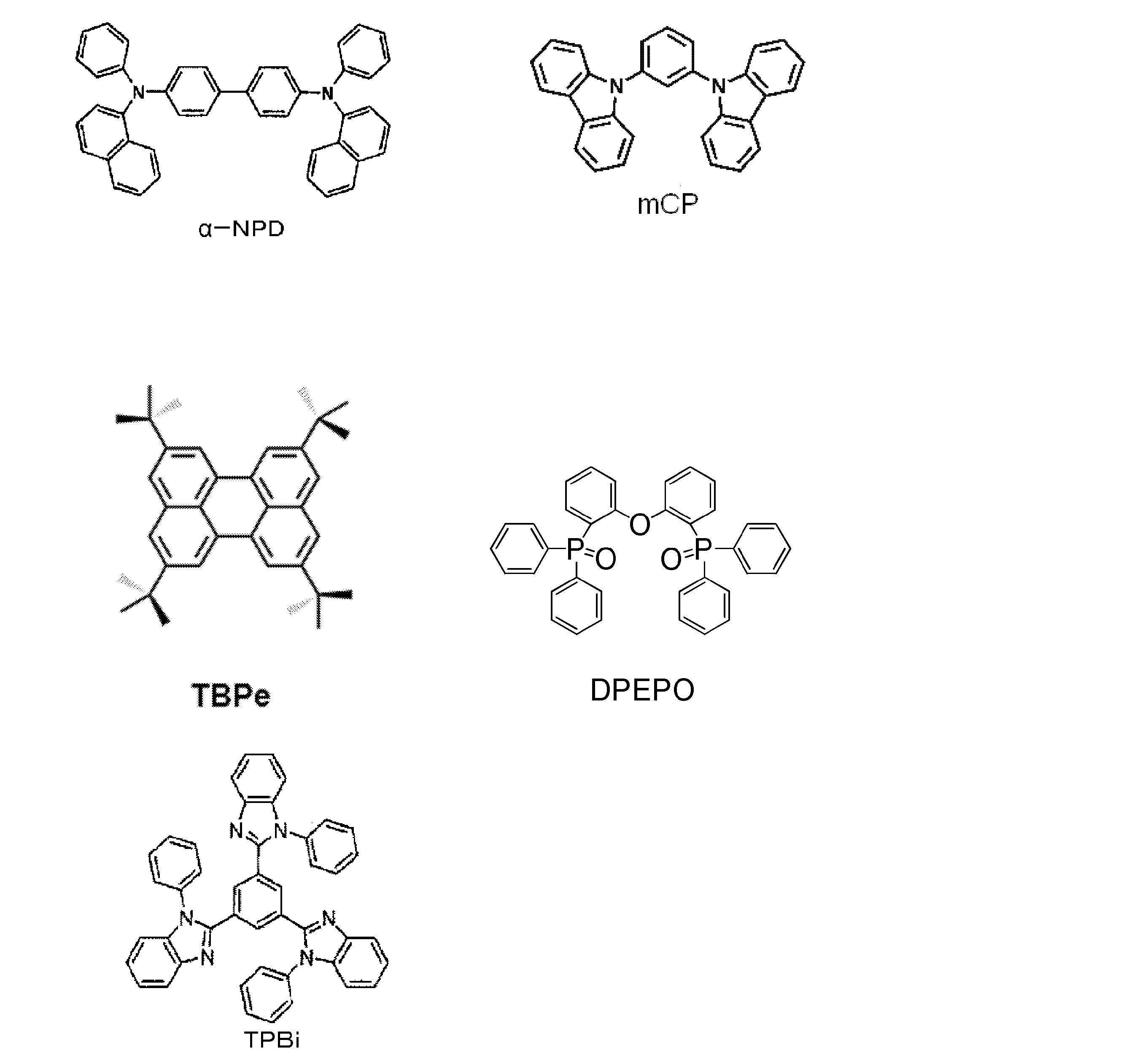
本発明の化合物はホストおよびアシストドーパントとして有用である。このため本発明の化合物は、有機エレクトロルミネッセンス素子などの有機発光素子用のホストおよびアシストドーパントとして効果的に用いられ、これにより発光効率が高い有機発光素子を提供することも可能である。このため、本発明は産業上の利用可能性が高い。
1 基板
2 陽極
3 正孔注入層
4 正孔輸送層
5 発光層
6 電子輸送層
7 陰極
2 陽極
3 正孔注入層
4 正孔輸送層
5 発光層
6 電子輸送層
7 陰極
Claims (18)
- 下記一般式(1)で表される化合物。
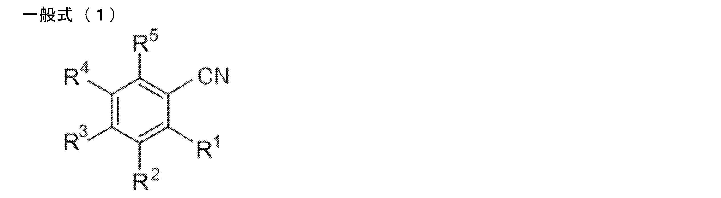
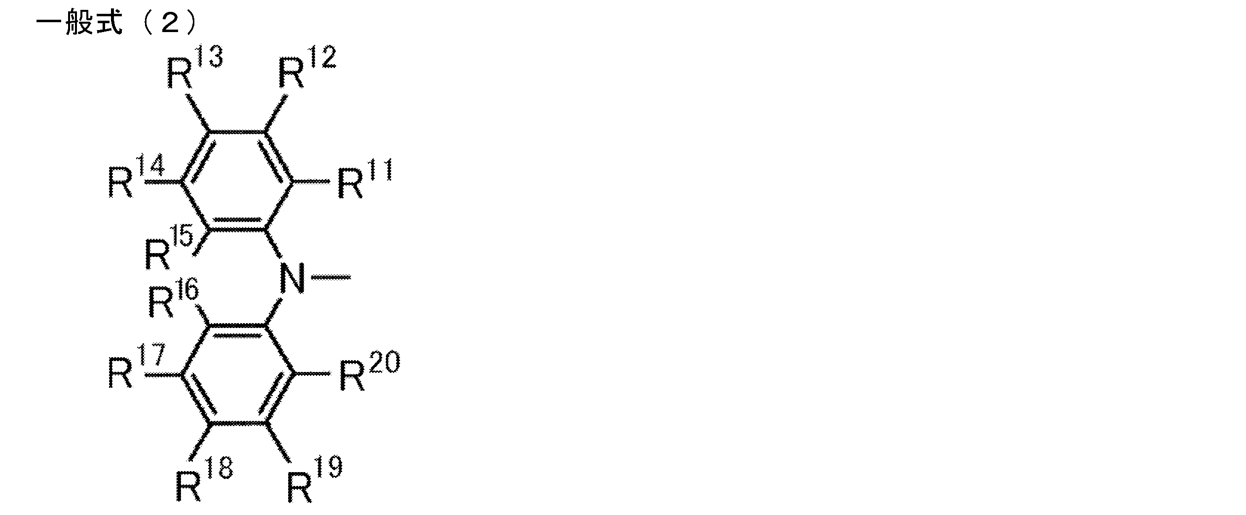
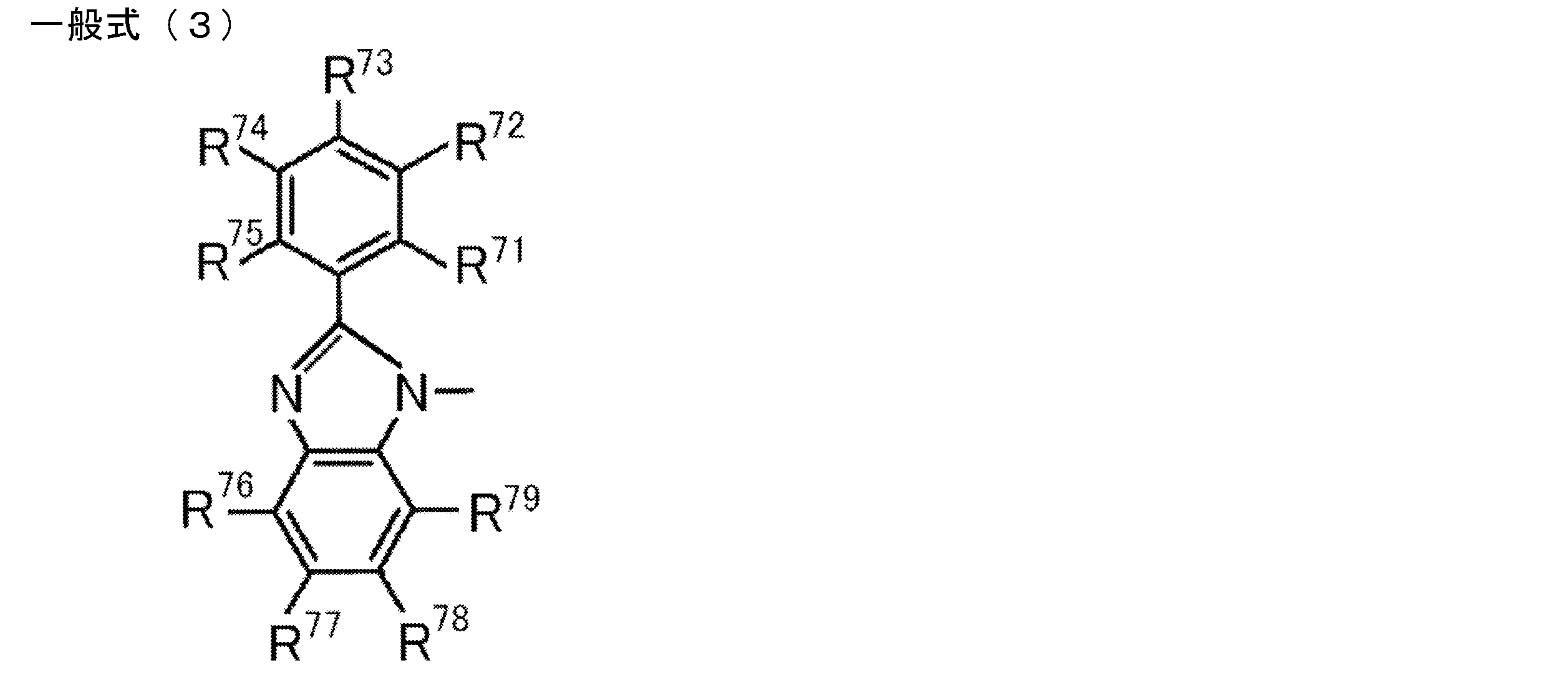
- 前記一般式(2)で表される基が、下記一般式(4)~(8)のいずれかで表される基であることを特徴とする請求項1に記載の化合物。

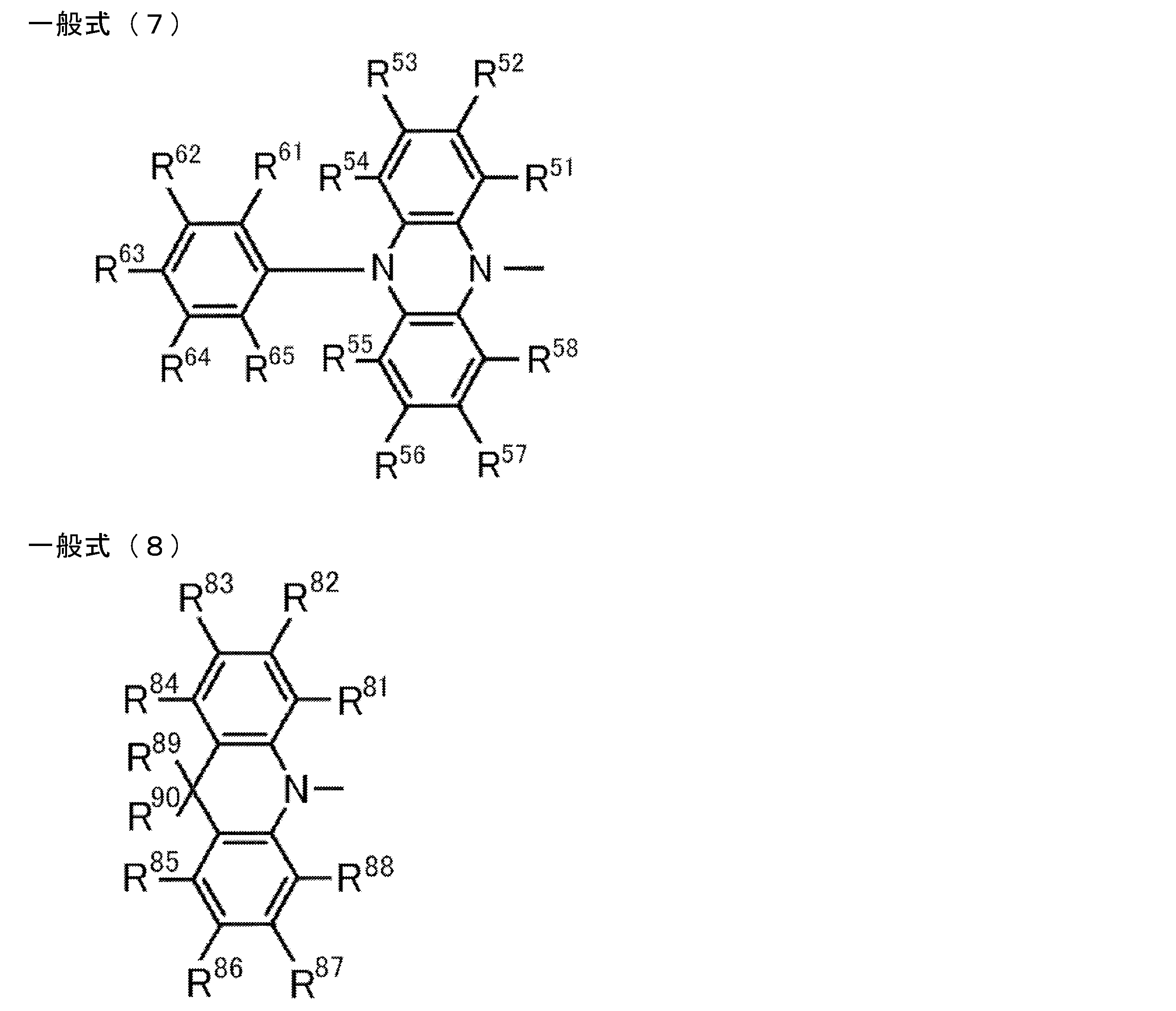
- 前記一般式(1)のR3が、前記一般式(2)で表される基であることを特徴とする請求項1または2に記載の化合物。
- 前記一般式(1)のR1、R2、R4、R5の少なくとも1つは、各々独立に炭素数1~3のアルキル基であることを特徴とする請求項3に記載の化合物。
- 前記一般式(1)のR1とR5が、前記一般式(2)で表される基であることを特徴とする請求項1または2に記載の化合物。
- 前記一般式(2)で表される基が、前記一般式(8)で表される基であることを特徴とする請求項1~5のいずれか1項に記載の化合物。
- 前記一般式(8)のR89およびR90が、ともに置換もしくは無置換のアリール基であることを特徴とする請求項6に記載の化合物。
- 前記一般式(1)で表される化合物からなる材料と、前記材料にドープされた発光材料を含むことを特徴とする混合物。
- 前記一般式(1)で表されるからなる材料と、前記材料にドープされた発光材料を含むことを特徴とする発光層。
- 前記一般式(1)で表される化合物は、発光層に含まれる有機化合物の中で最低励起一重項エネルギー準位が最も高い有機化合物であることを特徴とする請求項9に記載の発光層。
- 前記一般式(1)で表される化合物は、遅延蛍光体であることを特徴とする請求項9または10に記載の発光層。
- 前記一般式(1)で表される化合物は、最低励起一重項状態と77Kの最低励起三重項状態とのエネルギーの差ΔEstが0.3eV以下であることを特徴とする請求項11に記載の発光層。
- さらに、ホストを含むことを特徴とする請求項9に記載の発光層。
- 前記ホストと前記一般式(1)で表される化合物と前記発光材料が下記式(A)を満たし、且つ前記一般式(1)で表される化合物が遅延蛍光体であることを特徴とする請求項13に記載の発光層。
式(A) ES1(A)>ES1(B)>ES1(C)
[上式において、ES1(A)はホストの最低励起一重項エネルギー準位を表し、ES1(B)は一般式(1)で表される化合物の最低励起一重項エネルギー準位を表し、ES1(C)は発光材料の最低励起一重項エネルギー準位を表す。] - 前記一般式(1)で表される化合物は、最低励起一重項状態と77Kの最低励起三重項状態とのエネルギーの差ΔEstが0.3eV以下であることを特徴とする請求項14に記載の発光層。
- 請求項9~15のいずれか1項に記載の発光層を有することを特徴とする有機発光素子。
- 有機エレクトロルミネッセンス素子であることを特徴とする請求項16に記載の有機発光素子。
- 下記一般式(1)で表される化合物からなることを特徴とするアシストドーパント。
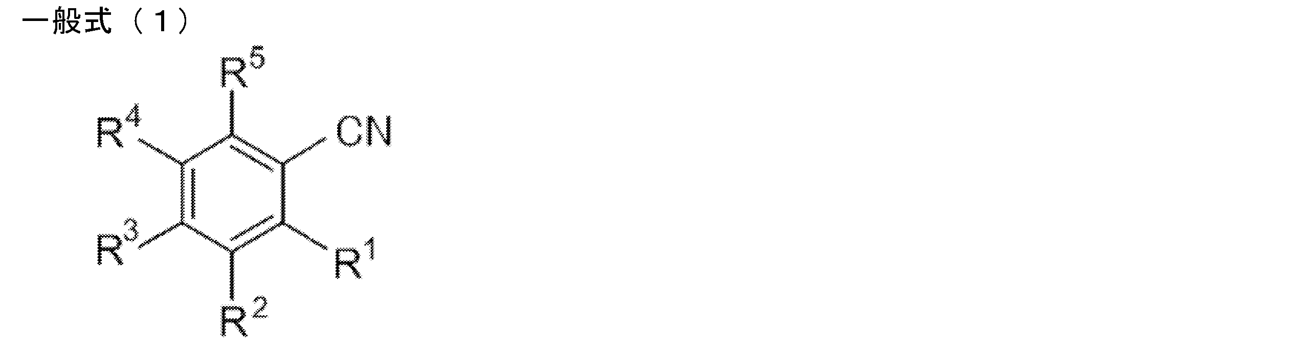


Applications Claiming Priority (4)
| Application Number | Priority Date | Filing Date | Title |
|---|---|---|---|
| JP2015-002632 | 2015-01-08 | ||
| JP2015002632 | 2015-01-08 | ||
| JP2015-130781 | 2015-06-30 | ||
| JP2015130781A JP6580392B2 (ja) | 2015-01-08 | 2015-06-30 | 化合物、混合物、発光層、有機発光素子およびアシストドーパント |
Publications (1)
| Publication Number | Publication Date |
|---|---|
| WO2016111196A1 true WO2016111196A1 (ja) | 2016-07-14 |
Family
ID=56355894
Family Applications (1)
| Application Number | Title | Priority Date | Filing Date |
|---|---|---|---|
| PCT/JP2015/086196 Ceased WO2016111196A1 (ja) | 2015-01-08 | 2015-12-25 | 化合物、混合物、発光層、有機発光素子およびアシストドーパント |
Country Status (1)
| Country | Link |
|---|---|
| WO (1) | WO2016111196A1 (ja) |
Cited By (5)
| Publication number | Priority date | Publication date | Assignee | Title |
|---|---|---|---|---|
| US20170263871A1 (en) * | 2016-12-30 | 2017-09-14 | Shanghai Tianma AM-OLED Co., Ltd. | Organic electroluminescent material and organic optoelectronic device |
| US20180198075A1 (en) * | 2015-07-03 | 2018-07-12 | Cynora Gmbh | Organic molecules for use in optoelectronic devices |
| WO2019163808A1 (ja) * | 2018-02-20 | 2019-08-29 | 国立大学法人九州大学 | 発光性粒子の製造方法、発光性粒子およびバイオイメージング材料 |
| US20210066636A1 (en) * | 2019-09-04 | 2021-03-04 | Lg Display Co., Ltd. | Organic light emitting diode and organic light emitting device having the diode |
| JP2023549984A (ja) * | 2020-10-30 | 2023-11-29 | ユニヴェルシテ・ドゥ・レンヌ | 円偏光oled発光層組成物 |
Citations (11)
| Publication number | Priority date | Publication date | Assignee | Title |
|---|---|---|---|---|
| WO2002059096A1 (en) * | 2001-01-25 | 2002-08-01 | Lumigen, Inc. | Processes and synthetic intermediates for preparing n-arylacridancarboxylic acid derivatives |
| JP2006028176A (ja) * | 2004-07-14 | 2006-02-02 | Samsung Sdi Co Ltd | フェニルカルバゾール化合物,及びそれを利用した有機電界発光素子 |
| WO2013085285A1 (ko) * | 2011-12-05 | 2013-06-13 | 고려대학교 산학협력단 | 정공전도특성을 갖는 염료감응 태양전지용 공흡착체 및 그를 포함하는 염료감응 태양전지 |
| WO2014017844A1 (ko) * | 2012-07-26 | 2014-01-30 | 주식회사 동진쎄미켐 | 아크리딘 유도체를 포함하는 유기발광 화합물 및 이를 포함하는 유기발광소자 |
| KR20140020208A (ko) * | 2012-08-07 | 2014-02-18 | 주식회사 동진쎄미켐 | 아크리딘 유도체를 포함하는 유기발광 화합물 및 이를 포함하는 유기발광소자 |
| KR20140076520A (ko) * | 2012-12-12 | 2014-06-20 | 에스에프씨 주식회사 | 유기발광 화합물 및 이를 포함하는 유기전계발광소자 |
| JP2014519481A (ja) * | 2011-04-18 | 2014-08-14 | メルク パテント ゲーエムベーハー | 電子デバイスのための化合物 |
| CN104099084A (zh) * | 2014-06-25 | 2014-10-15 | 吉林大学 | 一种蓝色有机电致荧光材料其制备方法及应用 |
| WO2014189122A1 (ja) * | 2013-05-24 | 2014-11-27 | 国立大学法人九州大学 | 化合物、発光材料および有機発光素子 |
| WO2015133501A1 (ja) * | 2014-03-07 | 2015-09-11 | 国立大学法人九州大学 | 発光材料、有機発光素子および化合物 |
| WO2015175678A1 (en) * | 2014-05-14 | 2015-11-19 | President And Fellows Of Harvard College | Organic light-emitting diode materials |
-
2015
- 2015-12-25 WO PCT/JP2015/086196 patent/WO2016111196A1/ja not_active Ceased
Patent Citations (11)
| Publication number | Priority date | Publication date | Assignee | Title |
|---|---|---|---|---|
| WO2002059096A1 (en) * | 2001-01-25 | 2002-08-01 | Lumigen, Inc. | Processes and synthetic intermediates for preparing n-arylacridancarboxylic acid derivatives |
| JP2006028176A (ja) * | 2004-07-14 | 2006-02-02 | Samsung Sdi Co Ltd | フェニルカルバゾール化合物,及びそれを利用した有機電界発光素子 |
| JP2014519481A (ja) * | 2011-04-18 | 2014-08-14 | メルク パテント ゲーエムベーハー | 電子デバイスのための化合物 |
| WO2013085285A1 (ko) * | 2011-12-05 | 2013-06-13 | 고려대학교 산학협력단 | 정공전도특성을 갖는 염료감응 태양전지용 공흡착체 및 그를 포함하는 염료감응 태양전지 |
| WO2014017844A1 (ko) * | 2012-07-26 | 2014-01-30 | 주식회사 동진쎄미켐 | 아크리딘 유도체를 포함하는 유기발광 화합물 및 이를 포함하는 유기발광소자 |
| KR20140020208A (ko) * | 2012-08-07 | 2014-02-18 | 주식회사 동진쎄미켐 | 아크리딘 유도체를 포함하는 유기발광 화합물 및 이를 포함하는 유기발광소자 |
| KR20140076520A (ko) * | 2012-12-12 | 2014-06-20 | 에스에프씨 주식회사 | 유기발광 화합물 및 이를 포함하는 유기전계발광소자 |
| WO2014189122A1 (ja) * | 2013-05-24 | 2014-11-27 | 国立大学法人九州大学 | 化合物、発光材料および有機発光素子 |
| WO2015133501A1 (ja) * | 2014-03-07 | 2015-09-11 | 国立大学法人九州大学 | 発光材料、有機発光素子および化合物 |
| WO2015175678A1 (en) * | 2014-05-14 | 2015-11-19 | President And Fellows Of Harvard College | Organic light-emitting diode materials |
| CN104099084A (zh) * | 2014-06-25 | 2014-10-15 | 吉林大学 | 一种蓝色有机电致荧光材料其制备方法及应用 |
Non-Patent Citations (2)
| Title |
|---|
| HIROKI NODA ET AL.: "4 A4-19 N,N- Biscarbazolylphenylaniline o Yusuru Ko-koritsu Netsu Kasseigata Chien Keiko Zairyo no Kaihatsu", CSJ: THE CHEMICAL SOCIETY OF JAPAN KOEN YOKOSHU, vol. 94th, no. 4, 12 March 2014 (2014-03-12), pages 1118, ISSN: 0285-7626 * |
| LAM, T. ET AL.: "Structure-Based Design of New Dihydrofolate Reductase Antibacterial Agents: 7-(Benzimidazol-1-yl)-2,4-diaminoquinazolines", JOURNAL OF MEDICINAL CHEMISTRY, vol. 57, no. 3, 2014, pages 651 - 668 * |
Cited By (11)
| Publication number | Priority date | Publication date | Assignee | Title |
|---|---|---|---|---|
| US20180198075A1 (en) * | 2015-07-03 | 2018-07-12 | Cynora Gmbh | Organic molecules for use in optoelectronic devices |
| US12262635B2 (en) * | 2015-07-03 | 2025-03-25 | Samsung Display Co., Ltd. | Organic molecules for use in optoelectronic devices |
| US20170263871A1 (en) * | 2016-12-30 | 2017-09-14 | Shanghai Tianma AM-OLED Co., Ltd. | Organic electroluminescent material and organic optoelectronic device |
| WO2019163808A1 (ja) * | 2018-02-20 | 2019-08-29 | 国立大学法人九州大学 | 発光性粒子の製造方法、発光性粒子およびバイオイメージング材料 |
| JPWO2019163808A1 (ja) * | 2018-02-20 | 2021-02-25 | 株式会社Kyulux | 発光性粒子の製造方法、発光性粒子およびバイオイメージング材料 |
| JP7294671B2 (ja) | 2018-02-20 | 2023-06-20 | 株式会社Kyulux | 発光性粒子の製造方法、発光性粒子およびバイオイメージング材料 |
| US12042547B2 (en) | 2018-02-20 | 2024-07-23 | Kyulux, Inc. | Method for producing luminescent particles, luminescent particles, and bioimaging material |
| US20210066636A1 (en) * | 2019-09-04 | 2021-03-04 | Lg Display Co., Ltd. | Organic light emitting diode and organic light emitting device having the diode |
| US12563884B2 (en) * | 2019-09-04 | 2026-02-24 | Lg Display Co., Ltd. | Organic light emitting diode and organic light emitting device having the diode |
| JP2023549984A (ja) * | 2020-10-30 | 2023-11-29 | ユニヴェルシテ・ドゥ・レンヌ | 円偏光oled発光層組成物 |
| JP7612888B2 (ja) | 2020-10-30 | 2025-01-14 | ユニヴェルシテ・ドゥ・レンヌ | 円偏光oled発光層組成物 |
Similar Documents
| Publication | Publication Date | Title |
|---|---|---|
| JP6526625B2 (ja) | 発光材料、有機発光素子および化合物 | |
| JP5669163B1 (ja) | 有機エレクトロルミネッセンス素子 | |
| JP6466913B2 (ja) | 発光材料、有機発光素子および化合物 | |
| JP6392240B2 (ja) | 発光材料、有機発光素子および化合物 | |
| TWI637937B (zh) | 發光材料、有機發光元件及化合物 | |
| JP6367189B2 (ja) | 発光材料、有機発光素子および化合物 | |
| CN105027314B (zh) | 电荷传输材料、主体材料、薄膜及有机发光元件 | |
| JP6469076B2 (ja) | 発光材料、有機発光素子および化合物 | |
| JP6383538B2 (ja) | 発光材料、有機発光素子および化合物 | |
| JP6293417B2 (ja) | 化合物、発光材料および有機発光素子 | |
| WO2015080183A1 (ja) | 発光材料、有機発光素子および化合物 | |
| CN106165138A (zh) | 有机发光元件、主体材料、发光材料及化合物 | |
| CN105980517A (zh) | 发光材料与使用其的延迟荧光体及有机发光元件 | |
| JP6647514B2 (ja) | 有機発光素子ならびにそれに用いる発光材料および化合物 | |
| TW201509920A (zh) | 化合物、發光材料及有機發光元件 | |
| JP6580392B2 (ja) | 化合物、混合物、発光層、有機発光素子およびアシストドーパント | |
| JP2017155003A (ja) | 化合物、キャリア輸送材料および有機発光素子 | |
| JP6534250B2 (ja) | 遅延蛍光体用ホスト材料、有機発光素子および化合物 | |
| JP2018111751A (ja) | 発光材料、化合物および有機発光素子 | |
| JP2016084283A (ja) | 化合物、発光材料および有機発光素子 |
Legal Events
| Date | Code | Title | Description |
|---|---|---|---|
| 121 | Ep: the epo has been informed by wipo that ep was designated in this application |
Ref document number: 15877069 Country of ref document: EP Kind code of ref document: A1 |
|
| NENP | Non-entry into the national phase |
Ref country code: DE |
|
| 122 | Ep: pct application non-entry in european phase |
Ref document number: 15877069 Country of ref document: EP Kind code of ref document: A1 |