WO2016103483A1 - チタンサファイヤレーザ装置、及び露光装置用レーザ装置、並びにチタンサファイヤ増幅器 - Google Patents
チタンサファイヤレーザ装置、及び露光装置用レーザ装置、並びにチタンサファイヤ増幅器 Download PDFInfo
- Publication number
- WO2016103483A1 WO2016103483A1 PCT/JP2014/084618 JP2014084618W WO2016103483A1 WO 2016103483 A1 WO2016103483 A1 WO 2016103483A1 JP 2014084618 W JP2014084618 W JP 2014084618W WO 2016103483 A1 WO2016103483 A1 WO 2016103483A1
- Authority
- WO
- WIPO (PCT)
- Prior art keywords
- light
- optical path
- seed light
- optical
- titanium
- Prior art date
- Legal status (The legal status is an assumption and is not a legal conclusion. Google has not performed a legal analysis and makes no representation as to the accuracy of the status listed.)
- Ceased
Links
Images










Classifications
-
- H—ELECTRICITY
- H01—ELECTRIC ELEMENTS
- H01S—DEVICES USING THE PROCESS OF LIGHT AMPLIFICATION BY STIMULATED EMISSION OF RADIATION [LASER] TO AMPLIFY OR GENERATE LIGHT; DEVICES USING STIMULATED EMISSION OF ELECTROMAGNETIC RADIATION IN WAVE RANGES OTHER THAN OPTICAL
- H01S3/00—Lasers, i.e. devices using stimulated emission of electromagnetic radiation in the infrared, visible or ultraviolet wave range
- H01S3/14—Lasers, i.e. devices using stimulated emission of electromagnetic radiation in the infrared, visible or ultraviolet wave range characterised by the material used as the active medium
- H01S3/16—Solid materials
- H01S3/1601—Solid materials characterised by an active (lasing) ion
- H01S3/162—Solid materials characterised by an active (lasing) ion transition metal
- H01S3/1625—Solid materials characterised by an active (lasing) ion transition metal titanium
-
- B—PERFORMING OPERATIONS; TRANSPORTING
- B23—MACHINE TOOLS; METAL-WORKING NOT OTHERWISE PROVIDED FOR
- B23K—SOLDERING OR UNSOLDERING; WELDING; CLADDING OR PLATING BY SOLDERING OR WELDING; CUTTING BY APPLYING HEAT LOCALLY, e.g. FLAME CUTTING; WORKING BY LASER BEAM
- B23K26/00—Working by laser beam, e.g. welding, cutting or boring
- B23K26/02—Positioning or observing the workpiece, e.g. with respect to the point of impact; Aligning, aiming or focusing the laser beam
- B23K26/06—Shaping the laser beam, e.g. by masks or multi-focusing
- B23K26/062—Shaping the laser beam, e.g. by masks or multi-focusing by direct control of the laser beam
- B23K26/0622—Shaping the laser beam, e.g. by masks or multi-focusing by direct control of the laser beam by shaping pulses
-
- H—ELECTRICITY
- H01—ELECTRIC ELEMENTS
- H01S—DEVICES USING THE PROCESS OF LIGHT AMPLIFICATION BY STIMULATED EMISSION OF RADIATION [LASER] TO AMPLIFY OR GENERATE LIGHT; DEVICES USING STIMULATED EMISSION OF ELECTROMAGNETIC RADIATION IN WAVE RANGES OTHER THAN OPTICAL
- H01S3/00—Lasers, i.e. devices using stimulated emission of electromagnetic radiation in the infrared, visible or ultraviolet wave range
- H01S3/05—Construction or shape of optical resonators; Accommodation of active medium therein; Shape of active medium
- H01S3/08—Construction or shape of optical resonators or components thereof
- H01S3/081—Construction or shape of optical resonators or components thereof comprising three or more reflectors
- H01S3/083—Ring lasers
-
- H—ELECTRICITY
- H01—ELECTRIC ELEMENTS
- H01S—DEVICES USING THE PROCESS OF LIGHT AMPLIFICATION BY STIMULATED EMISSION OF RADIATION [LASER] TO AMPLIFY OR GENERATE LIGHT; DEVICES USING STIMULATED EMISSION OF ELECTROMAGNETIC RADIATION IN WAVE RANGES OTHER THAN OPTICAL
- H01S3/00—Lasers, i.e. devices using stimulated emission of electromagnetic radiation in the infrared, visible or ultraviolet wave range
- H01S3/10—Controlling the intensity, frequency, phase, polarisation or direction of the emitted radiation, e.g. switching, gating, modulating or demodulating
- H01S3/10084—Frequency control by seeding
- H01S3/10092—Coherent seed, e.g. injection locking
-
- H—ELECTRICITY
- H01—ELECTRIC ELEMENTS
- H01S—DEVICES USING THE PROCESS OF LIGHT AMPLIFICATION BY STIMULATED EMISSION OF RADIATION [LASER] TO AMPLIFY OR GENERATE LIGHT; DEVICES USING STIMULATED EMISSION OF ELECTROMAGNETIC RADIATION IN WAVE RANGES OTHER THAN OPTICAL
- H01S3/00—Lasers, i.e. devices using stimulated emission of electromagnetic radiation in the infrared, visible or ultraviolet wave range
- H01S3/10—Controlling the intensity, frequency, phase, polarisation or direction of the emitted radiation, e.g. switching, gating, modulating or demodulating
- H01S3/13—Stabilisation of laser output parameters, e.g. frequency or amplitude
- H01S3/139—Stabilisation of laser output parameters, e.g. frequency or amplitude by controlling the mutual position or the reflecting properties of the reflectors of the cavity, e.g. by controlling the cavity length
-
- H—ELECTRICITY
- H01—ELECTRIC ELEMENTS
- H01S—DEVICES USING THE PROCESS OF LIGHT AMPLIFICATION BY STIMULATED EMISSION OF RADIATION [LASER] TO AMPLIFY OR GENERATE LIGHT; DEVICES USING STIMULATED EMISSION OF ELECTROMAGNETIC RADIATION IN WAVE RANGES OTHER THAN OPTICAL
- H01S3/00—Lasers, i.e. devices using stimulated emission of electromagnetic radiation in the infrared, visible or ultraviolet wave range
- H01S3/14—Lasers, i.e. devices using stimulated emission of electromagnetic radiation in the infrared, visible or ultraviolet wave range characterised by the material used as the active medium
- H01S3/16—Solid materials
- H01S3/163—Solid materials characterised by a crystal matrix
- H01S3/1631—Solid materials characterised by a crystal matrix aluminate
- H01S3/1636—Al2O3 (Sapphire)
-
- H—ELECTRICITY
- H01—ELECTRIC ELEMENTS
- H01S—DEVICES USING THE PROCESS OF LIGHT AMPLIFICATION BY STIMULATED EMISSION OF RADIATION [LASER] TO AMPLIFY OR GENERATE LIGHT; DEVICES USING STIMULATED EMISSION OF ELECTROMAGNETIC RADIATION IN WAVE RANGES OTHER THAN OPTICAL
- H01S3/00—Lasers, i.e. devices using stimulated emission of electromagnetic radiation in the infrared, visible or ultraviolet wave range
- H01S3/23—Arrangements of two or more lasers not provided for in groups H01S3/02 - H01S3/22, e.g. tandem arrangements of separate active media
-
- H—ELECTRICITY
- H01—ELECTRIC ELEMENTS
- H01S—DEVICES USING THE PROCESS OF LIGHT AMPLIFICATION BY STIMULATED EMISSION OF RADIATION [LASER] TO AMPLIFY OR GENERATE LIGHT; DEVICES USING STIMULATED EMISSION OF ELECTROMAGNETIC RADIATION IN WAVE RANGES OTHER THAN OPTICAL
- H01S3/00—Lasers, i.e. devices using stimulated emission of electromagnetic radiation in the infrared, visible or ultraviolet wave range
- H01S3/23—Arrangements of two or more lasers not provided for in groups H01S3/02 - H01S3/22, e.g. tandem arrangements of separate active media
- H01S3/2308—Amplifier arrangements, e.g. MOPA
- H01S3/2316—Cascaded amplifiers
-
- B—PERFORMING OPERATIONS; TRANSPORTING
- B23—MACHINE TOOLS; METAL-WORKING NOT OTHERWISE PROVIDED FOR
- B23K—SOLDERING OR UNSOLDERING; WELDING; CLADDING OR PLATING BY SOLDERING OR WELDING; CUTTING BY APPLYING HEAT LOCALLY, e.g. FLAME CUTTING; WORKING BY LASER BEAM
- B23K26/00—Working by laser beam, e.g. welding, cutting or boring
- B23K26/02—Positioning or observing the workpiece, e.g. with respect to the point of impact; Aligning, aiming or focusing the laser beam
- B23K26/06—Shaping the laser beam, e.g. by masks or multi-focusing
- B23K26/062—Shaping the laser beam, e.g. by masks or multi-focusing by direct control of the laser beam
- B23K26/0622—Shaping the laser beam, e.g. by masks or multi-focusing by direct control of the laser beam by shaping pulses
- B23K26/0624—Shaping the laser beam, e.g. by masks or multi-focusing by direct control of the laser beam by shaping pulses using ultrashort pulses, i.e. pulses of 1 ns or less
-
- H—ELECTRICITY
- H01—ELECTRIC ELEMENTS
- H01S—DEVICES USING THE PROCESS OF LIGHT AMPLIFICATION BY STIMULATED EMISSION OF RADIATION [LASER] TO AMPLIFY OR GENERATE LIGHT; DEVICES USING STIMULATED EMISSION OF ELECTROMAGNETIC RADIATION IN WAVE RANGES OTHER THAN OPTICAL
- H01S2301/00—Functional characteristics
- H01S2301/02—ASE (amplified spontaneous emission), noise; Reduction thereof
-
- H—ELECTRICITY
- H01—ELECTRIC ELEMENTS
- H01S—DEVICES USING THE PROCESS OF LIGHT AMPLIFICATION BY STIMULATED EMISSION OF RADIATION [LASER] TO AMPLIFY OR GENERATE LIGHT; DEVICES USING STIMULATED EMISSION OF ELECTROMAGNETIC RADIATION IN WAVE RANGES OTHER THAN OPTICAL
- H01S3/00—Lasers, i.e. devices using stimulated emission of electromagnetic radiation in the infrared, visible or ultraviolet wave range
- H01S3/005—Optical devices external to the laser cavity, specially adapted for lasers, e.g. for homogenisation of the beam or for manipulating laser pulses, e.g. pulse shaping
-
- H—ELECTRICITY
- H01—ELECTRIC ELEMENTS
- H01S—DEVICES USING THE PROCESS OF LIGHT AMPLIFICATION BY STIMULATED EMISSION OF RADIATION [LASER] TO AMPLIFY OR GENERATE LIGHT; DEVICES USING STIMULATED EMISSION OF ELECTROMAGNETIC RADIATION IN WAVE RANGES OTHER THAN OPTICAL
- H01S3/00—Lasers, i.e. devices using stimulated emission of electromagnetic radiation in the infrared, visible or ultraviolet wave range
- H01S3/005—Optical devices external to the laser cavity, specially adapted for lasers, e.g. for homogenisation of the beam or for manipulating laser pulses, e.g. pulse shaping
- H01S3/0071—Beam steering, e.g. whereby a mirror outside the cavity is present to change the beam direction
-
- H—ELECTRICITY
- H01—ELECTRIC ELEMENTS
- H01S—DEVICES USING THE PROCESS OF LIGHT AMPLIFICATION BY STIMULATED EMISSION OF RADIATION [LASER] TO AMPLIFY OR GENERATE LIGHT; DEVICES USING STIMULATED EMISSION OF ELECTROMAGNETIC RADIATION IN WAVE RANGES OTHER THAN OPTICAL
- H01S3/00—Lasers, i.e. devices using stimulated emission of electromagnetic radiation in the infrared, visible or ultraviolet wave range
- H01S3/09—Processes or apparatus for excitation, e.g. pumping
- H01S3/091—Processes or apparatus for excitation, e.g. pumping using optical pumping
- H01S3/094—Processes or apparatus for excitation, e.g. pumping using optical pumping by coherent light
- H01S3/094038—End pumping
-
- H—ELECTRICITY
- H01—ELECTRIC ELEMENTS
- H01S—DEVICES USING THE PROCESS OF LIGHT AMPLIFICATION BY STIMULATED EMISSION OF RADIATION [LASER] TO AMPLIFY OR GENERATE LIGHT; DEVICES USING STIMULATED EMISSION OF ELECTROMAGNETIC RADIATION IN WAVE RANGES OTHER THAN OPTICAL
- H01S3/00—Lasers, i.e. devices using stimulated emission of electromagnetic radiation in the infrared, visible or ultraviolet wave range
- H01S3/10—Controlling the intensity, frequency, phase, polarisation or direction of the emitted radiation, e.g. switching, gating, modulating or demodulating
- H01S3/10069—Memorized or pre-programmed characteristics, e.g. look-up table [LUT]
-
- H—ELECTRICITY
- H01—ELECTRIC ELEMENTS
- H01S—DEVICES USING THE PROCESS OF LIGHT AMPLIFICATION BY STIMULATED EMISSION OF RADIATION [LASER] TO AMPLIFY OR GENERATE LIGHT; DEVICES USING STIMULATED EMISSION OF ELECTROMAGNETIC RADIATION IN WAVE RANGES OTHER THAN OPTICAL
- H01S3/00—Lasers, i.e. devices using stimulated emission of electromagnetic radiation in the infrared, visible or ultraviolet wave range
- H01S3/10—Controlling the intensity, frequency, phase, polarisation or direction of the emitted radiation, e.g. switching, gating, modulating or demodulating
- H01S3/13—Stabilisation of laser output parameters, e.g. frequency or amplitude
- H01S3/1305—Feedback control systems
-
- H—ELECTRICITY
- H01—ELECTRIC ELEMENTS
- H01S—DEVICES USING THE PROCESS OF LIGHT AMPLIFICATION BY STIMULATED EMISSION OF RADIATION [LASER] TO AMPLIFY OR GENERATE LIGHT; DEVICES USING STIMULATED EMISSION OF ELECTROMAGNETIC RADIATION IN WAVE RANGES OTHER THAN OPTICAL
- H01S3/00—Lasers, i.e. devices using stimulated emission of electromagnetic radiation in the infrared, visible or ultraviolet wave range
- H01S3/10—Controlling the intensity, frequency, phase, polarisation or direction of the emitted radiation, e.g. switching, gating, modulating or demodulating
- H01S3/13—Stabilisation of laser output parameters, e.g. frequency or amplitude
- H01S3/139—Stabilisation of laser output parameters, e.g. frequency or amplitude by controlling the mutual position or the reflecting properties of the reflectors of the cavity, e.g. by controlling the cavity length
- H01S3/1394—Stabilisation of laser output parameters, e.g. frequency or amplitude by controlling the mutual position or the reflecting properties of the reflectors of the cavity, e.g. by controlling the cavity length by using an active reference, e.g. second laser, klystron or other standard frequency source
-
- H—ELECTRICITY
- H01—ELECTRIC ELEMENTS
- H01S—DEVICES USING THE PROCESS OF LIGHT AMPLIFICATION BY STIMULATED EMISSION OF RADIATION [LASER] TO AMPLIFY OR GENERATE LIGHT; DEVICES USING STIMULATED EMISSION OF ELECTROMAGNETIC RADIATION IN WAVE RANGES OTHER THAN OPTICAL
- H01S3/00—Lasers, i.e. devices using stimulated emission of electromagnetic radiation in the infrared, visible or ultraviolet wave range
- H01S3/23—Arrangements of two or more lasers not provided for in groups H01S3/02 - H01S3/22, e.g. tandem arrangements of separate active media
- H01S3/2308—Amplifier arrangements, e.g. MOPA
- H01S3/2325—Multi-pass amplifiers, e.g. regenerative amplifiers
-
- H—ELECTRICITY
- H01—ELECTRIC ELEMENTS
- H01S—DEVICES USING THE PROCESS OF LIGHT AMPLIFICATION BY STIMULATED EMISSION OF RADIATION [LASER] TO AMPLIFY OR GENERATE LIGHT; DEVICES USING STIMULATED EMISSION OF ELECTROMAGNETIC RADIATION IN WAVE RANGES OTHER THAN OPTICAL
- H01S3/00—Lasers, i.e. devices using stimulated emission of electromagnetic radiation in the infrared, visible or ultraviolet wave range
- H01S3/23—Arrangements of two or more lasers not provided for in groups H01S3/02 - H01S3/22, e.g. tandem arrangements of separate active media
- H01S3/2308—Amplifier arrangements, e.g. MOPA
- H01S3/2325—Multi-pass amplifiers, e.g. regenerative amplifiers
- H01S3/2333—Double-pass amplifiers
Definitions
- the present disclosure relates to a titanium-sapphire laser device using a titanium-sapphire crystal, a laser device for an exposure apparatus, and a titanium-sapphire amplifier.
- the semiconductor exposure apparatus With the miniaturization and high integration of semiconductor integrated circuits, improvement in resolution is required in a semiconductor exposure apparatus (hereinafter, the semiconductor exposure apparatus is simply referred to as "exposure apparatus"). For this reason, shortening of the wavelength of the light output from the light source for exposure is advanced.
- a gas laser device As a light source for exposure, a gas laser device is used in place of a conventional mercury lamp.
- KrF excimer laser devices that output ultraviolet light of wavelength 248 nm and ArF excimer laser devices that output ultraviolet light of wavelength 193 nm are used as gas laser devices for exposure.
- Spectral line widths are also referred to as spectral widths.
- a line narrowing module Line Narrow Module
- the narrowing element may be an etalon or a grating.
- the laser device whose spectrum width is narrowed as described above is called a narrow banded laser device.
- the titanium-sapphire laser device comprises a CW oscillation laser device that outputs seed light by CW oscillation in a single longitudinal mode, an optical resonator, and a titanium sapphire crystal disposed on an optical path in the optical resonator.
- an optical path length correction unit that changes the optical path length in the optical resonator so that the optical path length error approaches 0 at the timing immediately before the pulse laser light enters the titanium sapphire crystal. Good.
- Another titanium sapphire laser device reciprocates the seed light output from the master amplification oscillation unit including a master amplification oscillation unit including a CW oscillation laser unit that outputs seed light by CW oscillation in a single longitudinal mode.
- a second multi-pass amplifier may be provided that includes a second multi-pass and a second titanium sapphire crystal disposed on the second multi-pass. The number of round trips of the seed light in the second multipath amplifier may be less than or equal to the number of round trips of the seed light in the first multipath amplifier.
- a laser apparatus for an exposure apparatus includes: a CW oscillation laser apparatus that outputs seed light by CW oscillation in a single longitudinal mode; an optical resonator; and a titanium sapphire crystal disposed on an optical path in the optical resonator.
- a pulsed laser device for outputting pulsed laser light toward the titanium sapphire crystal, an optical path length of the positive integer multiple of the wavelength of the seed light and the optical path length in the optical resonator
- An error detector for detecting an error
- an optical path length correction unit for changing an optical path length in the optical resonator such that an optical path length error approaches 0 at a timing immediately before the pulse laser light enters the titanium sapphire crystal. It is also good.
- Another laser apparatus for exposure apparatus reciprocates the seed light output from the master amplification oscillation section including a master amplification oscillation section including a CW oscillation laser apparatus that outputs seed light by CW oscillation in a single longitudinal mode.
- a first multi-pass amplifier including a first multi-optical path for making the first multi-optical path and a first titanium-sapphire crystal provided on the first multi-optical path reciprocate the seed light output from the first multi-pass amplifier
- a second multi-pass amplifier including a second titanium sapphire crystal provided on the second multi-optical path.
- the number of round trips of the seed light in the second multipath amplifier may be less than or equal to the number of round trips of the seed light in the first multipath amplifier.
- the titanium-sapphire amplifier reciprocates pulsed seed light output from an amplification oscillator and transfers and forms an even number of incident beam images at a predetermined incident position of the seed light.
- the multipass optical system may include a titanium sapphire crystal provided on multiple light paths and amplifying the seed light.
- FIG. 1 schematically shows an example of the configuration of a laser apparatus for an exposure apparatus according to a comparative example.
- FIG. 2 schematically shows an example of the configuration of a narrow band titanium sapphire laser device according to a comparative example.
- FIG. 3 shows an example of the time-dependent change of the optical path length error when the optical path length error in the optical resonator is not corrected in the narrow band titanium sapphire laser device shown in FIG.
- FIG. 4 shows an example of the temporal change of the optical path length error when the optical path length error in the optical resonator is corrected in the narrow band titanium sapphire laser device shown in FIG.
- FIG. 1 schematically shows an example of the configuration of a laser apparatus for an exposure apparatus according to a comparative example.
- FIG. 2 schematically shows an example of the configuration of a narrow band titanium sapphire laser device according to a comparative example.
- FIG. 3 shows an example of the time-dependent change of the optical path length error when the optical path length error in the optical resonator is
- FIG. 5 shows an example of the change of the focal length due to the thermal lens effect in the titanium sapphire crystal.
- FIG. 6 schematically shows an example of the configuration of the MOPO section in the narrow band titanium sapphire laser device according to the first embodiment.
- FIG. 7 shows an example of the temporal change of the optical path length error when the optical path length error in the optical resonator is corrected in the narrow band titanium sapphire laser device shown in FIG.
- FIG. 8 is a main flowchart schematically showing an example of the flow of control of the optical path length in the optical resonator in the narrow band titanium sapphire laser device shown in FIG.
- FIG. 9 is a sub flowchart showing details of the process of step S105 in the main flowchart shown in FIG. FIG.
- FIG. 10 schematically shows an example of a method of measuring the minimum value of the optical path length error.
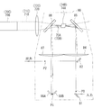
- FIG. 11 schematically illustrates an exemplary configuration of a multipass titanium sapphire amplifier in the narrow band titanium sapphire laser device according to the first embodiment.
- FIG. 12 schematically shows an optical equivalent view of a multipass optical system in the multipass titanium sapphire amplifier shown in FIG.
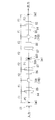
- FIG. 13 schematically shows a first variant of the multipass titanium sapphire amplifier shown in FIG.
- FIG. 14 schematically shows a second variant of the multipass titanium sapphire amplifier shown in FIG.
- FIG. 15 schematically shows one configuration example of the MOPO unit in the narrow band titanium sapphire laser device according to the second embodiment.
- FIG. 16 schematically illustrates an example of the configuration of a multipath amplification unit in the narrow band titanium sapphire laser device according to the second embodiment.
- FIG. 17 shows an example of the amplification characteristic of the multipath amplification unit shown in FIG.
- FIG. 18 schematically shows a modification of the multipath amplification unit shown in FIG.
- FIG. 19 schematically illustrates an exemplary configuration of an optical path length error detector.
- FIG. 20 schematically shows an example of the configuration of the light shutter.
- FIG. 21 shows an example of the hardware environment of the control unit.
- the present disclosure relates to, for example, a titanium-sapphire laser device using a titanium-sapphire crystal and a laser device for an exposure apparatus.
- FIG. 1 schematically shows an example of the configuration of a laser apparatus for an exposure apparatus of a comparative example to the embodiment of the present disclosure.
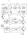
- the laser apparatus for exposure apparatus may include a solid-state laser system 1, an amplifier 2, a synchronization control unit 3, and high reflection mirrors 91 and 92.
- the solid state laser system 1 may include a first solid state laser device 11, a second solid state laser device 12, a synchronization circuit unit 13, a solid state laser control unit 14, and a wavelength conversion system 15.
- the first solid-state laser device 11 is an Nd: YVO 4 pulse laser device that outputs pulsed laser light having a wavelength of 1342 nm, and may be a laser device that oscillates in a single longitudinal mode.
- the second solid-state laser device 12 may include a narrow band titanium sapphire laser device 20 oscillating at a wavelength of 904 nm, an LBO (LiB 3 O 5 ) crystal 21 and a BBO ( ⁇ -BaB 2 O 4 ) crystal 22. .
- the wavelength conversion system 15 may include a high reflection mirror 16, a beam splitter 17, and a CLBO (CsLiB 6 O 10 ) crystal 18.
- the solid-state laser control unit 14 is configured, for example, to be able to transmit data, start up and stop signals with a control signal (not shown) to the first solid-state laser device 11 and the second solid-state laser device 12. May be
- the synchronization circuit unit 13 is configured such that the first pulse laser light output from the first solid-state laser device 11 and the second pulse laser light output from the second solid-state laser device 12 are CLBOs of the wavelength conversion system 15.
- the crystal 18 may be configured to be incident substantially simultaneously.
- the amplifier 2 includes an amplifier control unit 30, a charger 31, a trigger corrector 32, a pulse power module (PPM) 34 including a switch 33, a chamber 35, a partial reflection mirror 36 and an output coupling mirror 37. It may be.
- PPM pulse power module
- the chamber 35 may be provided with windows 39a and 39b.
- the chamber 35 may contain, for example, a laser gas containing Ar gas, F 2 gas, and Ne gas.
- a pair of discharge electrodes 38 may be disposed in the chamber 35. The pair of discharge electrodes 38 may be connected to the output terminal of the PPM 34.
- an optical resonator including the partial reflection mirror 36 and the output coupling mirror 37 may be configured.
- a partially reflecting film having a reflectance of 70 to 90% may be coated on a substrate made of a CaF 2 crystal that transmits light of wavelength 193 nm.
- a partially reflecting film having a reflectance of 10 to 20% may be coated on a substrate made of a CaF 2 crystal that transmits light of wavelength 193 nm.
- the oscillation trigger Tr ⁇ b> 0 may be input to the synchronization control unit 3 from the exposure apparatus control unit 5 of the exposure apparatus 4.
- the synchronization control unit 3 controls the amplifier control unit 30 so that the pair of discharge electrodes 38 discharge in synchronization with the pulsed laser light of wavelength 193 nm from the solid-state laser system 1 being injected into the optical resonator of the amplifier 2.
- And may be configured to output an oscillation trigger to the trigger correction unit 32 via
- the solid-state laser control unit 14 can output the pulsed laser light from the first solid-state laser device 11 and the second solid-state laser device 12, the first solid-state laser device 11 and the second solid-state laser device 12. You may prepare for driving with.
- the synchronization control unit 3 When receiving the oscillation trigger Tr0 from the exposure apparatus control unit 5 of the exposure apparatus 4, the synchronization control unit 3 outputs the oscillation trigger at a predetermined timing to the synchronization circuit unit 13 via the solid state laser control unit 14 of the solid state laser system 1. May be Also, when receiving the oscillation trigger Tr0 from the exposure apparatus control unit 5 of the exposure apparatus 4, the synchronization control unit 3 outputs the oscillation trigger to the trigger correction unit 32 at a predetermined timing via the amplifier control unit 30 of the amplifier 2 It is also good.
- the synchronization circuit unit 13 may output an oscillation trigger to each of the first solid-state laser device 11 and the narrow-band titanium sapphire laser device 20 of the second solid-state laser device 12 at a predetermined timing.
- the first solid-state laser apparatus 11 can output a first pulsed laser beam having a wavelength of 1342 nm.
- the second solid-state laser device 12 when an oscillation trigger is input to the narrow-band titanium sapphire laser device 20, pulsed laser light having a wavelength of 904 nm can be output from the narrow-band titanium sapphire laser device 20.
- the LBO crystal 21 and the BBO crystal 22 can generate second pulsed laser light, which is the fourth harmonic light with a wavelength of 226 nm.
- the first pulsed laser light of wavelength 1342 nm output from the first solid-state laser device 11 and the second pulsed laser light of wavelength 226 nm output from the second solid-state laser device 12 enter the wavelength conversion system 15 It can.
- the first and second pulse laser beams are substantially simultaneously incident on the CLBO crystal 18 by the high reflection mirror 16 and the beam splitter 17, and the first and second pulse laser beams are incident on the CLBO crystal 18. It can overlap.
- the CLBO crystal 18 can take the sum frequency of the wavelengths 226 nm and 1342 nm to generate pulsed laser light of wavelength 193 nm.
- the pulsed laser light can be incident on the partial reflection mirror 36 of the amplifier 2 through the high reflection mirrors 91 and 92.
- This pulsed laser light can be injected as seed light into the optical resonator of the amplifier 2 including the output coupling mirror 37 and the partial reflection mirror 36.
- a reversal distribution can be created by the discharge by the pair of discharge electrodes 38 in the chamber 35 of the amplifier 2.
- the trigger correction unit 32 may adjust the timing of the switch 33 of the PPM 34 so that the pulsed laser light from the solid-state laser system 1 with a wavelength of 193 nm is efficiently amplified by the amplifier 2.
- amplification and oscillation can be performed by the optical resonator of the amplifier 2, and the amplified pulsed laser light can be output from the output coupling mirror 37.
- FIG. 2 schematically illustrates an exemplary configuration of a narrow band titanium sapphire laser device 20 of a comparative example to the embodiment of the present disclosure.
- the narrow band titanium sapphire laser device 20 has a MOPO unit (master amplification and oscillation unit) 40, a fourth high reflection mirror 104, a fifth high reflection mirror 105, a second optical isolator 44B, and a sixth high
- the reflection mirror 106 and the multipath amplification unit 41 may be provided.
- the MOPO unit 40 may include an MO (master oscillator) 50 and a PO (amplification oscillator: power oscillator) 60.
- the MOPO unit 40 also includes a first optical isolator 44A, a first excitation pulse laser device 70A, a first condensing lens 72A, an optical path length correction unit 42, and an optical path length error detector 43. It may be.
- the MO 50 may be a CW oscillation laser device that oscillates CW (continuous wave) in a single longitudinal mode.
- the MO 50 may be, for example, a distributed feedback semiconductor laser that CW-oscillates in a single longitudinal mode and outputs the seed light 51 with a wavelength of 904 nm.
- a first optical isolator 44A may be disposed on the optical path between the MO 50 and the PO 60 to suppress transmission of return light.
- the first pulse laser apparatus for excitation 70A may be a pulse laser apparatus for outputting a first pulse laser beam 71A for excitation having a wavelength of 523 nm, which is the second harmonic wave of Nd: YLF pulse laser beam.
- the PO 60 may include an optical resonator and a titanium sapphire crystal 61 disposed on the optical path in the optical resonator. Both end faces of the titanium sapphire crystal 61 may be cut so as to be incident at Brewster's angle.
- the seed beam 51 and the first pulse laser beam 71A for excitation may be incident on the PO 60.
- the optical resonator of the PO 60 is a Z-shaped ring type optical resonator, and includes an output coupling mirror 62, a first high reflection mirror 101, a second high reflection mirror 102, and a third high reflection mirror 103. And may be included.
- the first high reflection mirror 101 may have a configuration in which a film that highly reflects light of wavelength 904 nm but transmits light partially is coated on a substrate that transmits light of wavelength 904 nm.
- the optical path length error detector 43 may be disposed on the optical path of the leaked light 52 so that the leaked light 52 of the seed light 51 from the first high reflection mirror 101 is incident.
- the second high reflection mirror 102 may be a dichroic mirror that highly transmits the first pulse laser light 71A to be excitation light, and highly reflects the seed light 51 with a wavelength of 904 nm.
- the third high reflection mirror 103 may be a mirror that highly reflects light of wavelength 904 nm.
- the third high reflection mirror 103 may be fixed to a mirror holder with a piezo element 46 including a piezo element.
- the moving direction of the mirror by the piezoelectric element may be substantially coincident with the normal direction of the mirror surface.
- the first excitation pulse laser device 70A and the first focusing lens 72A are configured to focus the first pulse laser beam 71A for excitation on the titanium sapphire crystal 61 through the first high reflection mirror 101. It may be arranged.
- the optical path length correction unit 42 may include a mirror holder 46 with a piezo element, a third high reflection mirror 103, and a proportional integral derivative (PID) controller 45.
- PID proportional integral derivative
- the PID controller 45 may be configured to control the position of the third high reflection mirror 103.
- the output signal of the optical path length error detector 43 may be input to the PID controller 45.
- the seed light 51 amplified by the PO 60 may be output through the output coupling mirror 62.
- the amplified seed light 51 is input to the multipath amplification unit 41 via the fourth high reflection mirror 104, the fifth high reflection mirror 105, the second optical isolator 44B, and the sixth high reflection mirror 106. As such, those optical elements may be arranged.
- the second optical isolator 44B may be disposed to suppress transmission of return light.
- the multi-pass amplification unit 41 includes a second excitation pulse laser device 70B, a third excitation pulse laser device 70C, a second focusing lens 72B, and a third focusing lens 72C. It is also good.
- the multipass amplifying unit 41 may also include a first multipass titanium sapphire amplifier 73A, a second multipass titanium sapphire amplifier 73B, and seventh to tenth high reflection mirrors 107 to 110.
- the second excitation pulse laser device 70B may be a pulse laser device that outputs a second pulse laser beam 71B for excitation having a wavelength of 523 nm, which is a second harmonic wave of Nd: YLF pulse laser beam.
- the third pulse laser apparatus for excitation 70C may be a pulse laser apparatus for outputting a third pulse laser beam 71C for excitation having a wavelength of 523 nm, which is the second harmonic wave of Nd: YLF pulse laser beam.
- the first multipass titanium sapphire amplifier 73A may include a first other titanium sapphire crystal 74A, as in the embodiment shown in FIG. 11 described later.
- the second multipass titanium sapphire amplifier 73B may include a second other titanium sapphire crystal 74B as in the embodiment shown in FIG. 11 described later.
- the first, second and third pulse laser devices for excitation 70 A, 70 B and 70 C may be configured to receive an oscillation trigger from the synchronous circuit unit 13.
- the MO 50 may output the seed light 51 by CW oscillation of the semiconductor laser in the single longitudinal mode.
- the seed light 51 can be input from the output coupling mirror 62 to the optical resonator PO60 via the first optical isolator 44A.
- the leaked light 52 of the seed light 51 can be output from the first high reflection mirror 101 by the seed light 51 traveling on the optical path of the optical resonator of PO60.
- the leaked light 52 may be input to the optical path length error detector 43, and an optical path length error signal may be output from the optical path length error detector 43.
- the first pulse laser beam 71A for excitation is output, and the titanium sapphire crystal 61 of PO 60 is pulsed. It can excite. Since the seed light 51 is already injected into the titanium sapphire crystal 61, the seed light 51 can be amplified in a pulse shape. As a result, laser light is oscillated by this optical resonator, and pulse light amplified seed light 51 can be output from the output coupling mirror 62.
- the pulsed-amplified seed light 51 passes through the fourth high reflection mirror 104, the fifth high reflection mirror 105, the second optical isolator 44B, and the sixth high reflection mirror 106. It may be incident on the multipath amplification unit 41.
- a seed light having a wavelength of 904 nm, which is amplified in a pulsed manner, to a first other titanium sapphire crystal 74A shown in FIG. 11 described later. 51 can be incident.
- the second pulsed laser beam 71B as excitation light from the second pumping pulse laser device 70B is incident on a first other titanium sapphire crystal 74A described later.
- the seed light 51 can be excited in a pulsed manner.
- the seed light 51 can be amplified a plurality of times by causing the pulsed laser light having a wavelength of 904 nm to multipass the first other titanium sapphire crystal 74A described later.
- the seed light 51 pulse-amplified by the first multipass titanium sapphire amplifier 73A passes through the eighth high reflection mirror 108 and the ninth high reflection mirror 109, and the second multipass titanium sapphire amplifier 73B.
- You can enter In the second multipass titanium-sapphire amplifier 73B the seed light 51 having a wavelength of 904 nm, which is amplified in a pulse shape, can be incident on a second other titanium-sapphire crystal 74B shown in FIG. 11 described later.
- the third pulsed laser beam 71C as excitation light from the third pulsed laser pulse device 71C is incident on a second other titanium sapphire crystal 74B described later.
- the seed light 51 can be excited in a pulsed manner.
- the seed light 51 can be amplified multiple times by causing the pulsed laser light of wavelength 904 nm to multipass the second other titanium sapphire crystal 74B described later.
- the seed light 51 amplified by the second multipass titanium sapphire amplifier 73 B may be incident on the LBO crystal 21 through the tenth high reflection mirror 110.
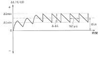
- FIG. 3 shows an example of temporal change of the optical path length error ⁇ L when the optical path length error ⁇ L in the optical resonator of PO 60 is not corrected in the narrow band titanium sapphire laser device 20 shown in FIG.
- FIG. 3 shows a time-dependent change immediately after the start of excitation with PO60.
- the horizontal axis in FIG. 3 represents time, and the vertical axis represents the optical path length error ⁇ L.
- the common path length error ⁇ L gradually drifts to the positive side by ⁇ Lc and changes, and the values of the maximum value Lmax and the minimum value Lmin can be alternately repeated for each excitation pulse.
- FIG. 4 shows an example of the temporal change of the optical path length error ⁇ L when the optical path length error ⁇ L in the optical resonator of PO 60 is corrected in the narrow band titanium sapphire laser device 20 shown in FIG.
- FIG. 4 shows a time-dependent change immediately after the start of excitation with PO60.
- the horizontal axis in FIG. 4 represents time, and the vertical axis represents the optical path length error ⁇ L.
- FIG. 5 shows an example of the focal length due to the thermal lens effect in a titanium sapphire crystal.
- the horizontal axis represents the input (W) of excitation light
- the vertical axis represents the focal length (mm) by the thermal lens effect.
- the focusing diameter may need to be 100 ⁇ m to 200 ⁇ m.
- the focal length of the thermal lens due to the thermal lens effect generated by the titanium sapphire crystals 74A and 74B may be short. As shown in FIG. 5, when the input of the excitation light is high, the focal length due to the thermal lens effect may be short.
- the focal length of the thermal lens due to this thermal lens effect becomes about 10 mm or less, the deterioration of beam characteristics after amplification is suppressed even if the position of the optical element of the optical system for multipassing titanium sapphire crystals 74A and 74B is adjusted. I could not do it.
- the number of times of multipassing of the seed light 51 in the first and second multipass titanium-sapphire amplifiers 73A and 73B is increased, deterioration of beam characteristics can be remarkable due to the thermal lens effect.
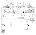
- FIG. 6 schematically shows an example of the configuration of the MOPO unit 40A as the main configuration of the narrow band titanium sapphire laser device 20 according to the first embodiment of the present disclosure.
- the narrow band titanium sapphire laser device 20 includes the MOPO unit 40A including the first light shutter 53A and the shift amount adder 54 in place of the MOPO unit 40 in the configuration of the comparative example shown in FIG. You may have.
- the narrow band titanium sapphire laser device 20 according to the present embodiment may further include an inverter 56, a delay circuit 57, and an error control unit 55 in addition to the configuration of the comparative example shown in FIG.
- the first optical shutter 53A may be disposed on the optical path of the leaked light 52 between the first high reflection mirror 101 and the optical path length error detector 43.
- the first optical shutter 53A may be closed during the period in which the first pulse laser beam 71A is incident on the titanium sapphire crystal 61 and may be controlled so as to be open in the period not incident on the titanium sapphire crystal 61 .
- the shift amount adder 54 may be disposed on the signal line between the optical path length error detector 43 and the PID controller 45.
- the error control unit 55 may transmit the data of the correction value Voffset to the shift amount adder 54 based on the optical path length error signal output from the optical path length error detector 43.
- the delay circuit 57 may receive the oscillation trigger of the synchronous circuit unit 13 and output a signal for controlling the opening and closing of the first optical shutter 53A via the inverter 56 after a predetermined delay time.
- Delay data Td for setting a delay time may be input from the error control unit 55 to the delay circuit 57.
- the optical path length correction unit 42 changes the optical path length in the optical resonator of PO60 so that the optical path length error ⁇ L approaches 0 at the timing immediately before the first pulse laser light 71A for excitation enters the titanium sapphire crystal 61. You may
- the error control unit 55 transmits delay data Td for setting the delay time to the delay circuit 57, and delays the opening / closing timing of the first optical shutter 53A with respect to the oscillation trigger from the synchronization circuit unit 13. Good.
- the error control unit 55 controls the optical shutter 53A so that the leaked light 52 of the seed light 51 amplified in a pulse shape is not detected by the optical path length error detector 43 in synchronization with the first pulsed laser light 71A for excitation. May be controlled.
- the error control unit 55 may control the delay circuit 57 so that the first optical shutter 53A is closed while the first pulse laser light 71A is incident on the titanium sapphire crystal 61.
- the error control unit 55 may also control the delay circuit 57 so as to open the first optical shutter 53A in a period in which the first pulse laser beam 71A is not incident on the titanium sapphire crystal 61.
- the light shutter 53A may be closed in a period in which the pulse-shaped amplified seed light 51 is incident, and may be controlled to be open in a period in which the pulse-shaped amplified seed light 51 is not incident. .
- the error control unit 55 reads data of temporal change of the optical path length error ⁇ L from the optical path length error detector 43, and the shift amount adder 54 corrects the correction value Voffset so that the minimum value ⁇ Lmin of the optical path length error ⁇ L approaches 0. Data may be sent. Thus, a voltage value obtained by adding the correction value Voffset from the shift amount adder 54 to the voltage V from the optical path length error detector 43, which is an optical path length error signal, can be input to the PID controller 45. By repeating these controls, the minimum value ⁇ Lmin of the optical path length error ⁇ L can approach zero.
- FIG. 7 shows an example of the temporal change of the optical path length error ⁇ L when the optical path length error ⁇ L in the optical resonator of PO 60 is corrected in the MOPO section 40A shown in FIG.
- the seed light 51 can be amplified in a pulsed manner in the state where the minimum value ⁇ Lmin of the optical path length error ⁇ L approaches zero.
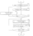
- FIG. 8 schematically shows an example of the flow of control of the optical path length in the optical resonator in the narrow band titanium sapphire laser device 20 shown in FIG.
- the error control unit 55 may measure the minimum value ⁇ Lmin of the optical path length error ⁇ L (step S105). Next, the error control unit 55 may transmit the data of the correction value Voffset to the shift amount adder 54 such that the minimum value ⁇ Lmin of the optical path length error ⁇ L approaches 0 (step S106). Next, the error control unit 55 may determine whether to cancel the control of the optical path length (step S107). If the error control unit 55 does not stop the control of the optical path length (step S107; N), the error control unit 55 may return to the process of step S105. The error control unit 55 may end the process when stopping the control of the optical path length (step S107; Y).
- FIG. 9 is a sub flowchart showing the details of the process of step S105.
- the error control unit 55 may reset and start the time T of a timer (not shown) (step S111).
- the error control unit 55 may read data of the optical path length error ⁇ L output from the optical path length error detector 43 (step S112).
- the error control unit 55 may store data of the time T and data of the optical path length error ⁇ L (step S113).
- the error control unit 55 may determine whether T ⁇ K, that is, whether the time T is equal to or longer than a predetermined time K (step S114). If the error control unit 55 determines that the time T is not longer than the predetermined time K (step S114; N), the error control unit 55 may return to the process of step S112.
- the error control unit 55 when it is determined that the time T is equal to or longer than the predetermined time K (step S104; Y), the error control unit 55 then reads the stored data and extracts data of a plurality of minimum values ⁇ Lmin. The average value ⁇ L minav may be calculated (step S115).
- FIG. 10 schematically shows an example of a method of measuring the minimum value ⁇ Lmin of the optical path length error ⁇ L.
- the horizontal axis may be time
- the vertical axis may be the optical path length error ⁇ L.
- data of the minimum value ⁇ Lmin of the optical path length error ⁇ L is detected as ⁇ Lmin (1), ⁇ Lmin (2), ⁇ Lmin (3), ⁇ Lmin (4) It may be done.
- the error control unit 55 may calculate the averaged value ⁇ Lminav of the minimum value ⁇ Lmin as follows.
- ⁇ Lminav ⁇ Lmin (1) + ⁇ Lmin (2) + ⁇ Lmin (3) + ⁇ Lmin (4) ⁇ / 4
- the error control unit 55 may set the obtained averaged value ⁇ Lminav as the minimum value ⁇ Lmin of the optical path length error ⁇ L (step S116), and return to the main flow of FIG.
- the minimum value ⁇ Lmin of the optical path length error ⁇ L is controlled to approach zero immediately before the seed light 51 is amplified in a pulse shape in the optical resonator of PO60.
- the efficiency of pulse amplification of the seed light 51 can be high.
- the output timing and pulse waveform of the seed light 51 amplified in a pulse shape can be stabilized.
- FIG. 11 schematically shows an example of the configuration of a multipass titanium sapphire amplifier in the multipass amplification unit 41 as the main part configuration of the narrow band titanium sapphire laser device 20 according to the first embodiment of the present disclosure .
- FIG. 12 schematically shows an optically equivalent view of the multipass optical system in the multipass titanium sapphire amplifier shown in FIG.
- FIG. 11 summarizes the configurations of the first multipass titanium sapphire amplifier 73A and the second multipass titanium sapphire amplifier 73B.
- the first multipass titanium sapphire amplifier 73A may include a multipass optical system 80 as a first multipass optical system.
- the second multipass titanium sapphire amplifier 73B may include a multipass optical system 80 as a second multipass optical system.
- Multipass optical system 80 may include an input mirror 81 and an output mirror 82.
- Multipass optical system 80 may also include focusing lens 84, dichroic mirror 85, dichroic mirror 86, focusing lens 87, and folding mirrors 88A and 88B.
- the first multipass titanium sapphire amplifier 73A comprises a first multipassage 75A formed by the multipass optical system 80 and a first other titaniumsapphire crystal 74A provided on the first multipassage 75A. May be included.
- the seed light 51 amplified by the PO 60 may be input to the first multipass titanium sapphire amplifier 73A through the input mirror 81 via the fourth high reflection mirror 104 and the like.
- the second multipass titanium-sapphire amplifier 73B comprises a second multipassage 75B formed by the multipass optical system 80 and a second other titaniumsapphire crystal 74B provided on the second multipassage 75B. May be included.
- the seed light 51 amplified by the first multipass titanium sapphire amplifier 73 A passes through the eighth high reflection mirror 108 and the ninth high reflection mirror 109, It may be input through the input mirror 81.
- the second focusing lens 72B is arranged such that the second pulse laser beam 71B is focused on the first other titanium sapphire crystal 74A through the dichroic mirror 86. It may be done.
- the second pulse laser beam 71B may be the excitation light for amplification output from the second excitation pulse laser device 70B.
- the dichroic mirror 85 and the dichroic mirror 86 may be disposed so that the seed light 51 passes back and forth through the first other titanium sapphire crystal 74A.
- the output mirror 82 outputs the seed light 51 after passing back and forth through the first other titanium sapphire crystal 74A toward the eighth high reflection mirror 108. It may be arranged as follows.
- the third focusing lens 72C is arranged so that the third pulse laser beam 71C is focused on the second other titanium sapphire crystal 74B via the dichroic mirror 86. It may be done.
- the third pulse laser beam 71C may be the excitation light for amplification output from the third pulse laser apparatus for excitation 70C.
- the dichroic mirror 85 and the dichroic mirror 86 may be disposed so that the seed light 51 passes back and forth through the second other titanium sapphire crystal 74B.
- the output mirror 82 outputs the seed light 51 after passing back and forth through the second other titanium sapphire crystal 74B toward the tenth high reflection mirror 110. It may be arranged as follows.
- the focal length f1 of the focusing lens 84 and the focal length f2 of the focusing lens 87 may be substantially the same predetermined focal length f.
- the condenser lens 84 and the condenser lens 87 have substantially the same predetermined focal length f, and the optical path length between the two lenses is approximately twice the predetermined focal length f. It may be arranged.
- the first and second other titanium sapphire crystals 74A and 74B may be disposed on the optical path approximately at the midpoint between the condensing lens 84 and the condensing lens 87, respectively.
- the dichroic mirror 85 is disposed on the optical path between the condenser lens 84 and the first or second other titanium sapphire crystal 74A, 74B so that the seed light 51 is reflected at approximately 45 degrees. May be
- the surface of the dichroic mirror 85 may be coated with a film that transmits excitation light highly and reflects the seed light 51 highly.
- the dichroic mirror 86 is disposed on the optical path between the condenser lens 87 and the first or second other titanium sapphire crystal 74A, 74B so that the seed light 51 is reflected at approximately 45 degrees. May be
- the surface of the dichroic mirror 86 may be coated with a film that transmits excitation light highly and reflects the seed light 51 highly.
- the input mirror 81 may be disposed such that the seed light 51 passes through the approximate center of the condenser lens 84.
- the folding mirrors 88A and 88B may constitute a pair of folding mirrors, and may be disposed to fold the seed light 51 incident through the condensing lens 87 to the condensing lens 87.
- the folding mirrors 88A and 88B are disposed such that the optical path length of the light path from the condensing lens 87 through the folding mirrors 88A and 88B to the condensing lens 87 is approximately twice the predetermined focal length f. May be
- the seed light 51 input to the multipass optical system 80 may be reflected by the input mirror 81 and may pass through the front focal position of the focusing lens 84 and may be incident on the approximate center of the focusing lens 84.
- the incident beam position P0 at which the incident beam image Im0 of the seed light 51 is formed may be substantially the same as the front focal position of the condensing lens 84.
- the seed light 51 can be amplified by passing through the first or second other titanium sapphire crystal 74A, 74B through the dichroic mirror 85.
- the amplified seed light 51 is reflected by the folding mirror 88A which is a predetermined incident position through the dichroic mirror 86 and the condenser lens 87, passes through the first transfer position P1, and is reflected by the folding mirror 88B. It is reflected and may enter the condenser lens 87 again.
- the first transfer position P1 as shown in FIG. 12, the first transfer image Im1 of the incident beam image Im0 may be transfer-imaged.
- this seed light 51 can be further amplified by passing through the first or second other titanium sapphire crystal 74A, 74B through the dichroic mirror 86.
- the amplified seed light 51 can be reflected by the output mirror 82 through the dichroic mirror 85 and the condenser lens 84, and can be output after passing through the second transfer position P2.
- the second transfer image Im2 of the incident beam image Im0 may be transfer-imaged.
- the seed light 51 can be passed back and forth through the first or second other titanium sapphire crystal 74A, 74B.
- the first transfer image Im1 of the incident beam image Im0 can be transferred and imaged at the first transfer position P1.
- the second transfer image Im2 of the incident beam image Im0 can be transferred and imaged at the second transfer position P2.
- the beam profile of the first transferred image Im1 is deteriorated, and the deterioration of the beam profile of the second transferred image Im2 is suppressed. It can be done.
- the multi-pass optical system 80 transfers and forms the incident beam image Im0 an even number of times as the first or second other seed light 51 It can be amplified by reciprocating with titanium sapphire crystals 74A and 74B. Thereby, distortion of the beam of amplified light due to the thermal lens effect can be suppressed.
- the focal length f1 of the focusing lens 84 and the focal length f2 of the focusing lens 87 are substantially the same predetermined focal length f
- the distances f1 and f2 may be different from each other.
- a multipass optical system may be configured to reciprocate the incident beam image Im0 a plurality of times while performing transfer image formation.
- the focal length f1 of the focusing lens 84 and the focal length f2 of the focusing lens 87 are different from each other, for example, as shown in FIG. 12, the focusing lens 84 and the focusing lens 87 are on the rear side of the focusing lens 84.
- the focal position may be arranged to substantially coincide with the front focal position of the condenser lens 87.
- the optical path length between the focusing lens 84 and the focusing lens 87 can be substantially the sum (f1 + f2) of the focal lengths of both focusing lenses.
- the folding mirror 88A so that the optical path length of the light path from the condensing lens 87 through the folding mirrors 88A and 88B to the condensing lens 87 is approximately twice the focal length f2 of the condensing lens 87.
- 88B may be arranged.
- the number of reciprocations of the seed light 51 is not limited to one reciprocation shown in FIG.
- the optical system may be a multipass optical system which reciprocates a plurality of times while causing the light emission.
- the number of round trips of the seed light 51 may be made different between the first multipass titanium sapphire amplifier 73A and the second multipass titanium sapphire amplifier 73B.
- the number of round trips of the seed light 51 in the second multipass titanium sapphire amplifier 73B may be less than or equal to the number of round trips of the seed light 51 in the first multipass titanium sapphire amplifier 73A.
- FIG. 13 shows a first modification of the multipass titanium sapphire amplifier shown in FIG. FIG. 13 collectively shows the configurations of the first multipass titanium sapphire amplifier 73A and the second multipass titanium sapphire amplifier 73B.
- the first multipass titanium sapphire amplifier 73A may include a multipass optical system 80A instead of the multipass optical system 80 shown in FIGS. 11 and 12 as a first multipass optical system.
- the second multipass titanium sapphire amplifier 73B may include a multipass optical system 80A as a second multipass optical system, instead of the multipass optical system 80 shown in FIGS. 11 and 12 described above.
- the multipass optical system 80A may include folding mirrors 83A and 83B, folding mirrors 83C and 83D, folding mirrors 88A and 88B, folding mirrors 88C and 88D, and folding mirrors 88E and 88F.
- the folding mirrors 88A and 88B may constitute a pair of folding mirrors, and may be disposed to fold the seed light 51 incident through the condensing lens 87 to the condensing lens 87.
- the folding mirrors 88A and 88B are disposed such that the optical path length of the light path from the condensing lens 87 through the folding mirrors 88A and 88B to the condensing lens 87 is approximately twice the predetermined focal length f. May be
- the folding mirrors 83A and 83B may constitute a pair of folding mirrors, and may be disposed so as to fold the seed light 51 incident through the condensing lens 84 to the condensing lens 84.
- the folding mirrors 83A and 83B are arranged such that the optical path length of the light path from the condensing lens 84 through the folding mirrors 83A and 83B to the condensing lens 84 is approximately twice the predetermined focal length f. May be
- the folding mirrors 88C and 88D may constitute a pair of folding mirrors, and may be disposed to fold the seed light 51 incident through the condensing lens 87 to the condensing lens 87.
- the folding mirrors 88C and 88D are disposed such that the optical path length of the light path from the condensing lens 87 through the folding mirrors 88C and 88D to the condensing lens 87 is approximately twice the predetermined focal length f. May be
- the folding mirrors 83C and 83D may constitute a pair of folding mirrors, and may be disposed to fold the seed light 51 incident through the condensing lens 84 to the condensing lens 84.
- the folding mirrors 83C and 83D are disposed such that the optical path length of the light path from the condensing lens 84 to the condensing lens 84 after passing through the folding mirrors 83C and 83D is approximately twice the predetermined focal length f. May be
- the folding mirrors 88E and 88F may constitute a pair of folding mirrors, and may be disposed to fold the seed light 51 incident through the condensing lens 87 to the condensing lens 87.
- the folding mirrors 88E and 88F are disposed such that the optical path length of the light path from the condensing lens 87 through the folding mirrors 88E and 88F to the condensing lens 87 is approximately twice the predetermined focal length f. May be
- the seed light 51 input to the multipass optical system 80A can be reflected by the input mirror 81, pass through the front focal position of the condensing lens 84 which is a predetermined incident position, and be incident on the approximate center of the condensing lens 84 .
- the incident beam position P0 at which the incident beam image Im0 of the seed light 51 is formed may be substantially the same as the front focal position of the condensing lens 84.
- the seed light 51 can be amplified by passing through the first or second other titanium sapphire crystal 74A, 74B through the dichroic mirror 85.
- the amplified seed light 51 is reflected by the folding mirror 88A through the dichroic mirror 86 and the condenser lens 87, passes through the first transfer position P1, is reflected by the folding mirror 88B, and is condensed again. It may be incident on the lens 87.
- the first transfer image Im1 of the incident beam image Im0 may be transferred and imaged at the first transfer position P1.
- this seed light 51 can be further amplified by passing through the first or second other titanium sapphire crystal 74A, 74B through the dichroic mirror 86.
- the amplified seed light 51 is reflected by the folding mirror 83A through the dichroic mirror 85 and the condensing lens 84, passes through the second transfer position P2, is reflected by the folding mirror 83B, and is condensed again. It may be incident on the lens 84. At the second transfer position P2, the second transfer image Im2 of the incident beam image Im0 may be transferred and imaged. Then, this seed light 51 can be further amplified by passing through the first or second other titanium sapphire crystal 74A, 74B again through the dichroic mirror 85.
- the amplified seed light 51 is reflected by the folding mirror 88C via the dichroic mirror 86 and the condensing lens 87, passes through the third transfer position P3, is reflected by the folding mirror 88D, and is condensed again. It may be incident on the lens 87. At the third transfer position P3, the third transfer image Im3 of the incident beam image Im0 may be transferred and imaged. Then, this seed light 51 can be further amplified by passing through the first or second other titanium sapphire crystal 74A, 74B through the dichroic mirror 86.
- the amplified seed light 51 is reflected by the folding mirror 83C through the dichroic mirror 85 and the condensing lens 84, passes through the fourth transfer position P4, is reflected by the folding mirror 83D, and is condensed again. It may be incident on the lens 84. At the fourth transfer position P4, the fourth transfer image Im4 of the incident beam image Im0 may be transfer-imaged. Then, this seed light 51 can be further amplified by passing through the first or second other titanium sapphire crystal 74A, 74B again through the dichroic mirror 85.
- the amplified seed light 51 is reflected by the folding mirror 88E through the dichroic mirror 86 and the condenser lens 87, passes through the fifth transfer position P5, is reflected by the folding mirror 88F, and is condensed again. It may be incident on the lens 87. At the fifth transfer position P5, the fifth transfer image Im5 of the incident beam image Im0 may be transfer-imaged. Then, this seed light 51 can be further amplified by passing through the first or second other titanium sapphire crystal 74A, 74B through the dichroic mirror 86.
- the amplified seed light 51 may be reflected by the output mirror 82 through the dichroic mirror 85 and the condenser lens 84, and may be output after passing through the sixth transfer position P6.
- the sixth transfer image Im6 of the incident beam image Im0 may be transfer-imaged at the sixth transfer position P6.
- the seed light 51 can be passed back and forth through the first or second other titanium sapphire crystal 74A, 74B.
- the incident beam image Im0 can be transferred and imaged as the first to sixth transferred images a total of six times.
- the beam profiles of the first, third and fifth transferred images deteriorate
- the beam profiles of the second, fourth and sixth transferred images deteriorate. Can be suppressed.
- the seed beam 51 is reciprocated and amplified by the first or second other titanium sapphire crystal 74A, 74B while transfer imaging of the incident beam image Im0 is performed even times by the multipass optical system 80A. obtain. Thereby, distortion of the beam of amplified light due to the thermal lens effect can be suppressed.
- FIG. 14 shows a second modification of the multipass titanium sapphire amplifier shown in FIG. FIG. 14 collectively shows the configurations of the first multipass titanium sapphire amplifier 73A and the second multipass titanium sapphire amplifier 73B.
- the first and second multipass titanium sapphire amplifiers 73A and 73B may each include a multipass optical system 80B instead of the multipass optical system 80A shown in FIG.
- Multipass optical system 80B may include dispersive prisms 89A, 89B.
- ASE Amptonified Spontaneous Emission: spontaneous emission amplified light
- dispersion prisms 89A, 89B may be inserted in the optical path. Alternatively, only one of the dispersing prisms 89A and 89B may be inserted.
- the dispersion prism 89A may be disposed between the folding mirrors 83A and 83C and the condenser lens 84.
- the dispersion prism 89 B may be disposed between the folding mirrors 88 C and 88 E and the condenser lens 87.
- FIG. 15 schematically shows an example of the configuration of the MOPO unit 40B as the main configuration of the narrow band titanium sapphire laser device 20 according to the second embodiment of the present disclosure.
- the narrow band titanium sapphire laser device 20 according to the present embodiment may include an MOPO unit 40B including a band pass filter 58 instead of the MOPO unit 40A in the configuration of the first embodiment shown in FIG.
- the narrow band titanium sapphire laser device 20 according to the present embodiment may further include a second optical shutter 53B in addition to the configuration of the first embodiment shown in FIG.
- the band pass filter 58 may be disposed on the optical path in the optical resonator of the PO 60.
- the band pass filter 58 may selectively transmit light in a wavelength range around the wavelength 904 nm, which is the wavelength of the seed light 51.
- the second light shutter 53 ⁇ / b> B may be disposed on the light path between the PO 60 and the multipass amplifier 41.
- the delay circuit 57 may receive the oscillation trigger of the synchronization circuit unit 13 and output a signal for controlling the opening and closing of the second optical shutter 53B after a predetermined delay time.
- the second optical shutter 53B is disposed between the PO 60 and the multi-pass amplifier 41, so that the second optical shutter 53B is transmitted.
- the variation of the pulse width of the pulse-shaped amplified seed light 51 and the fluctuation of the rise time of the pulse can be suppressed.
- the rise time and the pulse waveform may change somewhat with a slight error of the optical path length in the optical resonator. That is, even if the pulse of the seed light 51 incident on the second optical shutter 53B changes to some extent, the seed light emitted from the second optical shutter 53B by trimming this pulse by the second optical shutter 53B.
- the rise time of the 51 pulses and the pulse waveform can be stabilized.
- the optical path length in the optical resonator may be long. Therefore, by introducing a second optical shutter 53B that operates at high speed, opening and closing at a predetermined timing, and trimming the seed light 51 amplified in a pulse shape, the change in pulse width and the rise time of the pulse are Fluctuations can be suppressed. Since the final output from the narrow band titanium sapphire laser device 20 is determined by the multi-pass amplification unit 41, the influence of loss due to trimming by the second optical shutter 53B may be reduced.
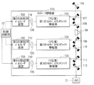
- FIG. 16 schematically shows an example of the configuration of a multi-pass amplification unit 41A as the main configuration of a narrow band titanium sapphire laser device 20 according to a second embodiment of the present disclosure.
- a multipass amplifying portion 41A including a third multipass titanium sapphire amplifier 73C is substituted for the multipass amplifying portion 41 in the configuration of the comparative example shown in FIG. You may have.
- the third multipass titanium sapphire amplifier 73C may include a third other titanium sapphire crystal.
- the third multipass titanium-sapphire amplifier 73C has a seed light with respect to the third other titanium-sapphire crystal in substantially the same manner as the configuration of the first and second multipass titanium-sapphire amplifiers 73A and 73B shown in FIG. 51 may be configured to pass back and forth.
- the multipass amplification unit 41A further includes a fourth excitation pulse laser device 70D, a fourth condenser lens 72D, an eleventh high reflection mirror 111, and a twelfth high reflection mirror 112. It is also good.
- the fourth pulse laser apparatus for excitation 70D may be a pulse laser apparatus that outputs a fourth pulse laser beam 71D for excitation.
- the first, second and third excitation pulse laser devices 70A, 70B and 70C, and the fourth excitation pulse laser device 70D are configured to receive an oscillation trigger input from the synchronization circuit unit 13. Good.
- the seed light 51 amplified by the second multipass titanium-sapphire amplifier 73B in the multipass amplifier 41A passes through the tenth high reflection mirror 110 and the eleventh high reflection mirror 111, and the third multipass titanium is amplified. It may be input to the sapphire amplifier 73C.
- the pulse light amplified seed light 51 having a wavelength of 904 nm may be incident on the third other titanium sapphire crystal.
- the fourth pulse laser beam 71D as excitation light from the fourth pulse laser apparatus for excitation 70D in synchronization with the incident timing of the seed beam 51 enters the third other titanium sapphire crystal as the seed beam 51. Can be pulsed.
- the seed light 51 can be amplified multiple times by causing the pulse laser light of wavelength 904 nm to multipass the third other titanium sapphire crystal.
- the seed light 51 amplified by the third multipass titanium sapphire amplifier 73 C may be incident on the LBO crystal 21 through the twelfth high reflection mirror 112.
- the multi-pass amplifying unit 41A for further amplifying the seed light 51 having a wavelength of 904 nm amplified in a pulse shape has a small amplification gain at this wavelength. It is necessary to optimize the number of multi-pulses of the multi-pass amplifier 41A and the number of multi-pass titanium sapphire amplifiers so that the focal length of the thermal lens in the titanium sapphire crystal is sufficiently long with respect to the crystal length.
- the number of multipaths in the first multipath titanium sapphire amplifier 73A may be three reciprocation. Further, the number of multipaths in the second multipass titanium sapphire amplifier 73B may be two reciprocation. Further, the number of multipaths in the third multipass titanium sapphire amplifier 73C may be one reciprocation.
- the focal length by the thermal lens effect in a titanium sapphire crystal may become short.
- the focal length of the thermal lens due to this thermal lens effect becomes about 10 mm or less, the optical element of the optical system for making the titanium sapphire crystal multipass, for example, the condenser lenses 84 and 87 shown in FIG. Even if the adjustment is made, deterioration of beam characteristics after amplification can not be suppressed. In particular, when the number of reciprocations is increased, the thermal lens effect in the titanium sapphire crystal may significantly degrade the beam characteristics.
- FIG. 17 shows an example of the amplification characteristic of the multipath amplification unit 41A shown in FIG.
- the upper part of FIG. 17 shows the relationship between the total number of reciprocations of the seed light 51 and the pulse energy of the amplified light of the seed light 51 in the first, second and third multipass titanium sapphire amplifiers 73A, 73B and 73C. Show.
- gain is saturated by reciprocating the first amplified light of the seed light 51 with small pulse energy output from the PO 60 three times. Can be amplified and output as a second amplified light.
- the second amplified light of the seed light 51 is reciprocated twice to be amplified until the gain is saturated and can be output as the third amplified light.
- the third multipass titanium-sapphire amplifier 73C by reciprocating the third amplified light of the seed light 51 one time, it can be amplified until the gain is saturated and output as the fourth amplified light.
- the lower part of FIG. 17 shows the relationship between the total number of round trips of the seed light 51 and the amplified light M 2 of the seed light 51 in the first, second and third multipass titanium sapphire amplifiers 73A, 73B and 73C.
- M 2 may mean the focusing performance of the laser beam characteristic.
- M 2 becomes larger in odd number of multipaths, and M 2 is improved by causing even number of multipaths. obtain. Having an even number of passes can be such that it is a multi-pass as it travels back and forth through a titanium sapphire crystal.
- the energy of the excitation light of each of the first, second and third multipass titanium sapphire amplifiers 73A, 73B and 73C has the following relationship with respect to the relationship of the input of the excitation light in order to sequentially increase the gain to be saturated.
- M 2 of the amplified light after one round trip can increase.
- the relationship between the increase in saturation and M 2 of the gain, the first multipath titanium sapphire amplifier 73A is 3 reciprocal
- second multipath titanium sapphire amplifier 73B is 2 reciprocating
- the amplifier 73C may make one round trip. Thereby, the improvement of amplification efficiency and the increase of M 2 can be suppressed.
- FIG. 18 schematically illustrates an example of the configuration of a multipath amplification unit 41B according to a modification of the present embodiment.
- the dispersion prism 59 may be disposed on the optical path between the first multipass titanium sapphire amplifier 73A and the second multipass titanium sapphire amplifier 73B as in the multipass amplification unit 41B shown in FIG. .
- the dispersion prism 59 can suppress the ASE light generated in the first other titanium sapphire crystal 74A of the first multipass titanium sapphire amplifier 73A from being incident on the second multipass titanium sapphire amplifier 73B.
- the dispersion prism 59 may be disposed on the optical path between the first multipass titanium sapphire amplifier 73A and the second multipass titanium sapphire amplifier 73B.
- a dispersive prism 59 may be disposed in the other light path of the seed light 51 as necessary.
- the optical path length error detector 43 may be a detector according to the Hansch-Couillaud method.
- the Hansch-Couillaud method measures the polarization characteristics of the leaked light 52 of the seed light 51 from the optical resonator to determine the optical path length error between the positive integer multiple of the wavelength of the seed light 51 and the optical path length in the optical resonator. It may be a method of detecting ⁇ L.
- the optical path length error detector 43 subtracts the ⁇ / 2 plate 91, the ⁇ / 4 plate 92, the polarizer 93, the high reflection mirror 94, the first light sensor 95A, and the second light sensor 95B.
- Device 96 may be included.
- the light intensity signals of the first light sensor 95A and the second light sensor 95B are subtracted by the subtractor 96, and when the value of the subtractor 96 is 0, the positive integer multiple of the wavelength of the seed light 51 and the optical resonance
- the optical path length in the vessel can be matched.
- the subtracted voltage value may be output from the subtractor 96 in accordance with the optical path length error ⁇ L.
- the error control unit 55 reading the voltage value output from the subtractor 96, the state of the optical path length error ⁇ L can be measured.
- the Hansch-Couillaud method is shown as a method of measuring the optical path length error ⁇ L, but without being limited to this method, the Pound-Derever-Hall method or the phase sensitive detection method may be used. Good.
- FIG. 20 shows an example of the configuration of the light shutter 310.
- the light shutter 310 may include a Pockels cell 394 and a polarizer 396.
- the Pockels cell 394 may include a high voltage power supply 393, a first electrode 395a, a second electrode 395b, and an electro-optic crystal 395c.
- the first electrode 395a and the second electrode 395b may be disposed opposite to each other, and an electro-optic crystal 395c may be disposed therebetween.
- the high voltage power supply 393 may be controlled by the transmittance setting unit 311 and the synchronization circuit 312.
- the high voltage power supply 393 may receive a control signal of the light shutter 310 from the transmittance setting unit 311 or the synchronization circuit 312.
- the high voltage power supply 393 receives an open signal for opening the optical shutter 310 as a control signal of the optical shutter 310
- the high voltage power supply 393 generates a predetermined high voltage which is not 0 V, and the voltage is set to the first electrode 395a and the It may be applied between the two electrodes 395b.
- the high voltage power supply 393 sets the voltage applied between the first electrode 395a and the second electrode 395b to 0 V when receiving a close signal for closing the light shutter 310 as a control signal of the light shutter 310. May be
- the Pockels cell 394 may have a function equivalent to a ⁇ / 2 plate when a predetermined high voltage is applied between the first electrode 395 a and the second electrode 395 b.
- a predetermined high voltage is not applied between the first electrode 395a and the second electrode 395b
- the light in the linear polarization direction perpendicular to the paper surface is in the same polarization state as the electro-optical crystal. It may be transmitted 395 c and reflected by polarizer 396.
- light linearly polarized in the direction perpendicular to the paper surface can be indicated by black circles drawn on the laser light path.
- the phase when a predetermined high voltage is applied, the phase is shifted by ⁇ / 2, and linearly polarized light in the direction perpendicular to the paper surface can be converted into linearly polarized light in the direction including the paper surface.
- light linearly polarized in the direction including the paper surface can be indicated by an arrow perpendicular to the optical path drawn on the laser optical path. This light may be transmitted through polarizer 396.
- the light shutter 310 can transmit light while applying a high voltage to the electro-optical crystal 395 c.
- the Pockels cell 394 Since the Pockels cell 394 has a response of about 1 ns, it can be used as a high speed light shutter. Further, as the light shutter 310, for example, an AO (acousto-optic) element may be used. In this case, it has a response on the order of several hundred ns and can be used.
- the transmittance can also be changed by changing the voltage applied between the first electrode 395a and the second electrode 395b in accordance with control from the transmittance setting unit 311.
- a polarizer and a ⁇ / 2 plate may be further added to the optical path on the upstream side to function as an optical isolator.
- the left side may be the upstream side
- the right side may be the downstream side.
- the optical isolator can highly transmit light from both the upstream side and the downstream side when a predetermined high voltage is applied between the first electrode 395a and the second electrode 395b of the Pockels cell 394. . That is, the optical isolator can be open. When a predetermined high voltage is not applied between the first electrode 395a and the second electrode 395b, transmission of light from both the upstream side and the downstream side can be suppressed. That is, the optical isolator can be closed.
- FIG. 21 is a block diagram illustrating an exemplary hardware environment in which various aspects of the disclosed subject matter can be implemented.
- the exemplary hardware environment 100 of FIG. 21 includes a processing unit 1000, storage unit 1005, user interface 1010, parallel I / O controller 1020, serial I / O controller 1030, A / D, D / A.
- the converter 1040 may be included, the configuration of the hardware environment 100 is not limited to this.
- the processing unit 1000 may include a central processing unit (CPU) 1001, a memory 1002, a timer 1003, and an image processing unit (GPU) 1004.
- Memory 1002 may include random access memory (RAM) and read only memory (ROM).
- the CPU 1001 may be any commercially available processor. Dual microprocessors or other multiprocessor architectures may be used as the CPU 1001.
- FIG. 21 may be interconnected to perform the processes described in this disclosure.
- the processing unit 1000 may load and execute a program stored in the storage unit 1005.
- the processing unit 1000 may also read data from the storage unit 1005 together with the program. Further, the processing unit 1000 may write data to the storage unit 1005.
- the CPU 1001 may execute a program read from the storage unit 1005.
- the memory 1002 may be a work area for temporarily storing a program executed by the CPU 1001 and data used for the operation of the CPU 1001.
- the timer 1003 may measure a time interval and output the measurement result to the CPU 1001 according to the execution of the program.
- the GPU 1004 may process image data according to a program read from the storage unit 1005, and may output the processing result to the CPU 1001.
- the parallel I / O controller 1020 includes processing units 1000 such as the synchronization control unit 3, the exposure apparatus control unit 5, the synchronization circuit unit 13, the amplifier control unit 30, the charger 31, the shift amount adder 54, and the error control unit 55. And may be connected to, and control communication between the processing unit 1000 and the parallel I / O devices.
- the serial I / O controller 1030 may be connected to a plurality of serial I / O devices that can communicate with the processing unit 1000, such as the delay circuit 57 and the error control unit 55, and the processing unit 1000 and the plurality of serial I It may control communication with the / O device.
- the A / D, D / A converter 1040 may be connected to various sensors, for example, analog devices such as the optical path length error detector 43 via an analog port, and communication between the processing unit 1000 and these analog devices Control, or A / D and D / A conversion of communication contents may be performed.
- the user interface 1010 may display the progress of the program executed by the processing unit 1000 to the operator so that the operator can instruct the processing unit 1000 to stop the program or execute the interrupt routine.
- Exemplary hardware environment 100 may be applied to configurations such as solid state laser control 14 in the present disclosure.
- the controllers may be implemented in a distributed computing environment, ie, an environment where tasks are performed by processing units that are linked through a communications network.
- an exposure apparatus laser control unit (not shown) that integrally controls the solid-state laser control unit 14, the synchronization control unit 3, and the amplifier control unit 30 via a communication network such as Ethernet (registered trademark) or the Internet. It may be connected to each other.
- program modules may be stored on both local and remote memory storage devices.
Landscapes
- Physics & Mathematics (AREA)
- Electromagnetism (AREA)
- Optics & Photonics (AREA)
- Engineering & Computer Science (AREA)
- Plasma & Fusion (AREA)
- Chemical & Material Sciences (AREA)
- Crystallography & Structural Chemistry (AREA)
- Inorganic Chemistry (AREA)
- Mechanical Engineering (AREA)
- Lasers (AREA)
- Exposure And Positioning Against Photoresist Photosensitive Materials (AREA)
Abstract
本開示によるチタンサファイヤレーザ装置は、シングル縦モードでCW発振してシード光を出力するCW発振レーザ装置と、光共振器と、この光共振器内の光路上に配置されたチタンサファイヤ結晶とを含み、シード光が入射する増幅発振器と、チタンサファイヤ結晶に向けてパルスレーザ光を出力するパルスレーザ装置と、シード光の波長の正の整数倍と光共振器内の光路長との光路長誤差を検出する誤差検出器と、パルスレーザ光がチタンサファイヤ結晶に入射する直前のタイミングで光路長誤差が0に近づくように光共振器内の光路長を変化させる光路長補正部とを備えてもよい。
Description
本開示は、チタンサファイヤ結晶を用いたチタンサファイヤレーザ装置、及び露光装置用レーザ装置、並びにチタンサファイヤ増幅器に関する。
半導体集積回路の微細化、高集積化につれて、半導体露光装置においては解像力の向上が要請されている(半導体露光装置を以下、単に「露光装置」という)。このため、露光用光源から出力される光の短波長化が進められている。露光用光源には、従来の水銀ランプに代わってガスレーザ装置が用いられている。現在、露光用のガスレーザ装置としては、波長248nmの紫外線を出力するKrFエキシマレーザ装置並びに、波長193nmの紫外線を出力するArFエキシマレーザ装置が用いられている。
現在の露光技術としては、露光装置側の投影レンズとウエハ間の間隙を液体で満たして、当該間隙の屈折率を変えることによって、露光用光源の見かけの波長を短波長化する液浸露光が実用化されている。ArFエキシマレーザ装置を露光用光源として用いて液浸露光が行われた場合は、ウエハには水中における波長134nmの紫外光が照射される。この技術をArF液浸露光という。ArF液浸露光はArF液浸リソグラフィーとも呼ばれる。
KrF、ArFエキシマレーザ装置の自然発振におけるスペクトル線幅は約350~400pmと広いため、露光装置側の投影レンズによってウエハ上に縮小投影されるレーザ光(紫外線光)の色収差が発生して解像力が低下する。そこで色収差が無視できる程度となるまでガスレーザ装置から出力されるレーザ光のスペクトル線幅を狭帯域化する必要がある。スペクトル線幅はスペクトル幅とも呼ばれる。このためガスレーザ装置のレーザ共振器内には狭帯域化素子を有する狭帯域化モジュール(Line Narrow Module)が設けられ、この狭帯域化モジュールによりスペクトル幅の狭帯域化が実現されている。なお、狭帯域化素子はエタロンやグレーティング等であってもよい。このようにスペクトル幅が狭帯域化されたレーザ装置を狭帯域化レーザ装置という。
本開示によるチタンサファイヤレーザ装置は、シングル縦モードでCW発振してシード光を出力するCW発振レーザ装置と、光共振器と、この光共振器内の光路上に配置されたチタンサファイヤ結晶とを含み、シード光が入射する増幅発振器と、チタンサファイヤ結晶に向けてパルスレーザ光を出力するパルスレーザ装置と、シード光の波長の正の整数倍と光共振器内の光路長との光路長誤差を検出する誤差検出器と、パルスレーザ光がチタンサファイヤ結晶に入射する直前のタイミングで光路長誤差が0に近づくように光共振器内の光路長を変化させる光路長補正部とを備えてもよい。
本開示による他のチタンサファイヤレーザ装置は、シングル縦モードでCW発振してシード光を出力するCW発振レーザ装置、を含むマスタ増幅発振部と、マスタ増幅発振部から出力されたシード光を往復させる第1のマルチ光路と、この第1のマルチ光路上に設けられた第1のチタンサファイヤ結晶とを含む第1のマルチパス増幅器と、第1のマルチパス増幅器から出力されたシード光を往復させる第2のマルチ光路と、この第2のマルチ光路上に設けられた第2のチタンサファイヤ結晶とを含む第2のマルチパス増幅器とを備えてもよい。第2のマルチパス増幅器におけるシード光の往復回数を、第1のマルチパス増幅器におけるシード光の往復回数以下であってもよい。
本開示による露光装置用レーザ装置は、シングル縦モードでCW発振してシード光を出力するCW発振レーザ装置と、光共振器と、この光共振器内の光路上に配置されたチタンサファイヤ結晶とを含み、シード光が入射する増幅発振器と、チタンサファイヤ結晶に向けてパルスレーザ光を出力するパルスレーザ装置と、シード光の波長の正の整数倍と光共振器内の光路長との光路長誤差を検出する誤差検出器と、パルスレーザ光がチタンサファイヤ結晶に入射する直前のタイミングで光路長誤差が0に近づくように光共振器内の光路長を変化させる光路長補正部とを備えてもよい。
本開示による他の露光装置用レーザ装置は、シングル縦モードでCW発振してシード光を出力するCW発振レーザ装置、を含むマスタ増幅発振部と、マスタ増幅発振部から出力されたシード光を往復させる第1のマルチ光路と、この第1のマルチ光路上に設けられた第1のチタンサファイヤ結晶とを含む第1のマルチパス増幅器と、第1のマルチパス増幅器から出力されたシード光を往復させる第2のマルチ光路と、この第2のマルチ光路上に設けられた第2のチタンサファイヤ結晶とを含む第2のマルチパス増幅器とを備えてもよい。第2のマルチパス増幅器におけるシード光の往復回数を、第1のマルチパス増幅器におけるシード光の往復回数以下であってもよい。
本開示によるチタンサファイヤ増幅器は、増幅発振器から出力されたパルス状のシード光を往復させると共に、前記シード光の所定の入射位置における入射ビーム像を偶数回、転写結像させるマルチパス光学システムと、このマルチパス光学システム内のマルチ光路上に設けられ、前記シード光を増幅するチタンサファイヤ結晶とを備えてもよい。
本開示のいくつかの実施形態を、単なる例として、添付の図面を参照して以下に説明する。
図1は、比較例に係る露光装置用レーザ装置の一構成例を概略的に示す。
図2は、比較例に係る狭帯域チタンサファイヤレーザ装置の一構成例を概略的に示す。
図3は、図2に示した狭帯域チタンサファイヤレーザ装置において、光共振器内の光路長誤差を補正しなかった場合の光路長誤差の経時変化の一例を示す。
図4は、図2に示した狭帯域チタンサファイヤレーザ装置において、光共振器内の光路長誤差を補正した場合の光路長誤差の経時変化の一例を示す。
図5は、チタンサファイヤ結晶における熱レンズ効果による焦点距離の変化の一例を示す。
図6は、第1の実施形態に係る狭帯域チタンサファイヤレーザ装置におけるMOPO部の一構成例を概略的に示す。
図7は、図6に示した狭帯域チタンサファイヤレーザ装置において、光共振器内の光路長誤差を補正した場合の光路長誤差の経時変化の一例を示す。
図8は、図6に示した狭帯域チタンサファイヤレーザ装置における光共振器内の光路長の制御の流れの一例を概略的に示すメインのフローチャートである。
図9は、図8に示したメインのフローチャートにおけるステップS105の処理の詳細を示すサブのフローチャートである。
図10は、光路長誤差の最小値の計測方法の一例を概略的に示す。
図11は、第1の実施形態に係る狭帯域チタンサファイヤレーザ装置におけるマルチパスチタンサファイヤ増幅器の一構成例を概略的に示す。
図12は、図11に示したマルチパスチタンサファイヤ増幅器におけるマルチパス光学システムの光学的な等価図を模式的に示す。
図13は、図11に示したマルチパスチタンサファイヤ増幅器の第1の変形例を概略的に示す。
図14は、図11に示したマルチパスチタンサファイヤ増幅器の第2の変形例を概略的に示す。
図15は、第2の実施形態に係る狭帯域チタンサファイヤレーザ装置におけるMOPO部の一構成例を概略的に示す。
図16は、第2の実施形態に係る狭帯域チタンサファイヤレーザ装置におけるマルチパス増幅部の一構成例を概略的に示す。
図17は、図16に示したマルチパス増幅部の増幅特性の一例を示す。
図18は、図16に示したマルチパス増幅部の変形例を概略的に示す。
図19は、光路長誤差検出器の一構成例を概略的に示す。
図20は、光シャッタの一構成例を概略的に示す。
図21は、制御部のハードウエア環境の一例を示す。
<内容>
[1.概要]
[2.比較例]
2.1 露光装置用レーザ装置
2.1.1 構成(図1)
2.1.2 動作
2.2 狭帯域チタンサファイヤレーザ装置
2.2.1 構成(図2)
2.2.2 動作
2.2.3 課題(図3~図5)
[3.第1の実施形態]
3.1 MOPO部(図6~図10)
3.1.1 構成
3.1.2 動作
3.1.3 作用
3.2 マルチパス増幅部
3.2.1 構成(図11、図12)
3.2.2 動作
3.2.3 作用
3.2.4 変形例
3.2.4.1 第1の変形例(図13)
3.2.4.2 第2の変形例(図14)
[4.第2の実施形態]
4.1 MOPO部(図15)
4.1.1 構成
4.1.2 作用
4.2 マルチパス増幅部
4.2.1 構成(図16)
4.2.2 動作及び作用(図17)
4.2.3 変形例(図18)
[5.光路長誤差検出器の構成例](図19)
5.1 構成
5.2 動作
5.3 変形例
[6.光シャッタの構成例](図20)
6.1 構成
6.2 動作
[7.制御部のハードウエア環境](図21)
[8.その他]
[1.概要]
[2.比較例]
2.1 露光装置用レーザ装置
2.1.1 構成(図1)
2.1.2 動作
2.2 狭帯域チタンサファイヤレーザ装置
2.2.1 構成(図2)
2.2.2 動作
2.2.3 課題(図3~図5)
[3.第1の実施形態]
3.1 MOPO部(図6~図10)
3.1.1 構成
3.1.2 動作
3.1.3 作用
3.2 マルチパス増幅部
3.2.1 構成(図11、図12)
3.2.2 動作
3.2.3 作用
3.2.4 変形例
3.2.4.1 第1の変形例(図13)
3.2.4.2 第2の変形例(図14)
[4.第2の実施形態]
4.1 MOPO部(図15)
4.1.1 構成
4.1.2 作用
4.2 マルチパス増幅部
4.2.1 構成(図16)
4.2.2 動作及び作用(図17)
4.2.3 変形例(図18)
[5.光路長誤差検出器の構成例](図19)
5.1 構成
5.2 動作
5.3 変形例
[6.光シャッタの構成例](図20)
6.1 構成
6.2 動作
[7.制御部のハードウエア環境](図21)
[8.その他]
以下、本開示の実施形態について、図面を参照しながら詳しく説明する。以下に説明される実施形態は、本開示のいくつかの例を示すものであって、本開示の内容を限定するものではない。また、各実施形態で説明される構成及び動作の全てが本開示の構成及び動作として必須であるとは限らない。なお、同一の構成要素には同一の参照符号を付して、重複する説明を省略する。
[1.概要]
本開示は、例えば、チタンサファイヤ結晶を用いたチタンサファイヤレーザ装置、及び露光装置用レーザ装置に関する。
本開示は、例えば、チタンサファイヤ結晶を用いたチタンサファイヤレーザ装置、及び露光装置用レーザ装置に関する。
[2.比較例]
まず、本開示の実施形態に対する比較例のチタンサファイヤレーザ装置、及び露光装置用レーザ装置について説明する。
まず、本開示の実施形態に対する比較例のチタンサファイヤレーザ装置、及び露光装置用レーザ装置について説明する。
(2.1 露光装置用レーザ装置)
(2.1.1 構成)
図1は、本開示の実施形態に対する比較例の露光装置用レーザ装置の一構成例を概略的に示している。
(2.1.1 構成)
図1は、本開示の実施形態に対する比較例の露光装置用レーザ装置の一構成例を概略的に示している。
露光装置用レーザ装置は、固体レーザシステム1と、増幅器2と、同期制御部3と、高反射ミラー91,92とを備えてもよい。
固体レーザシステム1は、第1の固体レーザ装置11と、第2の固体レーザ装置12と、同期回路部13と、固体レーザ制御部14と、波長変換システム15とを含んでもよい。
第1の固体レーザ装置11は、波長1342nmのパルスレーザ光を出力するNd:YVO4パルスレーザ装置で、シングル縦モードで発振するレーザ装置であってもよい。第2の固体レーザ装置12は、波長904nmで発振する狭帯域チタンサファイヤレーザ装置20と、LBO(LiB3O5)結晶21と、BBO(β-BaB2O4)結晶22とを含んでもよい。
波長変換システム15は、高反射ミラー16と、ビームスプリッタ17と、CLBO(CsLiB6O10)結晶18とを含んでいてもよい。
固体レーザ制御部14は、例えば、第1の固体レーザ装置11と第2の固体レーザ装置12とに、図示しない制御信号でデータの送信や立ち上げや停止信号の送信ができるように構成されていてもよい。
同期回路部13は、第1の固体レーザ装置11から出力された第1のパルスレーザ光と、第2の固体レーザ装置12から出力された第2のパルスレーザ光とが波長変換システム15のCLBO結晶18に略同時に入射するように構成されていてもよい。
増幅器2は、増幅器制御部30と、充電器31と、トリガ補正器32と、スイッチ33を含むパルスパワーモジュール(PPM)34と、チャンバ35と、部分反射ミラー36と出力結合ミラー37とを含んでいてもよい。
チャンバ35にはウインドウ39a,39bが設けられていてもよい。チャンバ35の中には例えばArガスとF2ガスとNeガスとを含むレーザガスが入っていてもよい。チャンバ35の中には1対の放電電極38が配置されていてもよい。1対の放電電極38は、PPM34の出力端子に接続されていてもよい。
増幅器2において、部分反射ミラー36と出力結合ミラー37とを含む光共振器が構成されていてもよい。部分反射ミラー36は例えば、波長193nmの光を透過するCaF2結晶からなる基板に、反射率が70~90%の部分反射膜がコートされていてもよい。出力結合ミラー37は例えば、波長193nmの光を透過するCaF2結晶からなる基板に反射率が10~20%の部分反射膜がコートされていてもよい。
同期制御部3には、露光装置4の露光装置制御部5から発振トリガTr0が入力されてもよい。同期制御部3は、固体レーザシステム1からの波長193nmのパルスレーザ光が増幅器2の光共振器に注入されるのと同期して1対の放電電極38が放電するように、増幅器制御部30を介してトリガ補正器32に発振トリガを出力するように構成されていてもよい。
(2.1.2 動作)
固体レーザ制御部14は、第1の固体レーザ装置11と第2の固体レーザ装置12とからパルスレーザ光を出力可能となるように、第1の固体レーザ装置11と第2の固体レーザ装置12との運転準備をしてもよい。同期制御部3は、露光装置4の露光装置制御部5から発振トリガTr0を受信すると、固体レーザシステム1の固体レーザ制御部14を介して同期回路部13に所定のタイミングで発振トリガを出力してもよい。同期制御部3はまた、露光装置4の露光装置制御部5から発振トリガTr0を受信すると、増幅器2の増幅器制御部30を介して、トリガ補正器32に所定のタイミングで発振トリガを出力してもよい。
固体レーザ制御部14は、第1の固体レーザ装置11と第2の固体レーザ装置12とからパルスレーザ光を出力可能となるように、第1の固体レーザ装置11と第2の固体レーザ装置12との運転準備をしてもよい。同期制御部3は、露光装置4の露光装置制御部5から発振トリガTr0を受信すると、固体レーザシステム1の固体レーザ制御部14を介して同期回路部13に所定のタイミングで発振トリガを出力してもよい。同期制御部3はまた、露光装置4の露光装置制御部5から発振トリガTr0を受信すると、増幅器2の増幅器制御部30を介して、トリガ補正器32に所定のタイミングで発振トリガを出力してもよい。
同期回路部13は、第1の固体レーザ装置11と第2の固体レーザ装置12の狭帯域チタンサファイヤレーザ装置20とにそれぞれ、所定のタイミングで発振トリガを出力してもよい。第1の固体レーザ装置11からは波長1342nmの第1のパルスレーザ光が出力され得る。
第2の固体レーザ装置12において、狭帯域チタンサファイヤレーザ装置20に発振トリガが入力されると、狭帯域チタンサファイヤレーザ装置20から波長904nmのパルスレーザ光が出力され得る。そして、LBO結晶21とBBO結晶22とによって、波長226nmの第4高調波光である第2のパルスレーザ光が生成され得る。第1の固体レーザ装置11から出力された波長1342nmの第1のパルスレーザ光と、第2の固体レーザ装置12から出力された波長226nmの第2のパルスレーザ光は、波長変換システム15に入射し得る。
波長変換システム15では、高反射ミラー16とビームスプリッタ17とによってCLBO結晶18に第1及び第2のパルスレーザ光が略同時に入射し、CLBO結晶18上で第1及び第2のパルスレーザ光が重なり得る。CLBO結晶18では、波長226nmと波長1342nmとの和周波を取り、波長193nmのパルスレーザ光を生成し得る。このパルスレーザ光が高反射ミラー91,92を介して、増幅器2の部分反射ミラー36に入射し得る。
このパルスレーザ光はシード光として、出力結合ミラー37と部分反射ミラー36を含む増幅器2の光共振器中に注入され得る。この注入に同期して、増幅器2のチャンバ35内では1対の放電電極38による放電で反転分布を作り得る。ここで、トリガ補正器32は、波長193nmの固体レーザシステム1からのパルスレーザ光が増幅器2で効率よく増幅されるようにPPM34のスイッチ33のタイミングを調整してもよい。その結果、増幅器2の光共振器によって増幅発振して、出力結合ミラー37から増幅されたパルスレーザ光を出力し得る。
(2.2 狭帯域チタンサファイヤレーザ装置)
(2.2.1 構成)
図2は、本開示の実施形態に対する比較例の狭帯域チタンサファイヤレーザ装置20の一構成例を概略的に示している。
(2.2.1 構成)
図2は、本開示の実施形態に対する比較例の狭帯域チタンサファイヤレーザ装置20の一構成例を概略的に示している。
狭帯域チタンサファイヤレーザ装置20は、MOPO部(マスタ増幅発振部)40と、第4の高反射ミラー104と、第5の高反射ミラー105と、第2の光アイソレータ44Bと、第6の高反射ミラー106と、マルチパス増幅部41とを備えてもよい。
MOPO部40は、MO(マスタオシレータ)50と、PO(増幅発振器:パワーオシレータ)60とを含んでいてもよい。MOPO部40はまた、第1の光アイソレータ44Aと、第1の励起用パルスレーザ装置70Aと、第1の集光レンズ72Aと、光路長補正部42と、光路長誤差検出器43とを含んでいてもよい。
MO50は、シングル縦モードでCW(連続波)発振するCW発振レーザ装置であってもよい。MO50は例えば、シングル縦モードでCW発振して波長904nmのシード光51を出力する分布帰還型の半導体レーザであってもよい。MO50とPO60との間の光路上には、戻り光の透過を抑制するための第1の光アイソレータ44Aが配置されていてもよい。
第1の励起用パルスレーザ装置70Aは、Nd:YLFパルススレーザ光の第2高調波光である波長523nmの励起用の第1のパルスレーザ光71Aを出力するパルスレーザ装置であってもよい。
PO60は、光共振器と、この光共振器内の光路上に配置されたチタンサファイヤ結晶61とを含んでもよい。チタンサファイヤ結晶61の両端面はブリュースター角で入射するようにカットされていてもよい。PO60には、シード光51と励起用の第1のパルスレーザ光71Aとが入射してもよい。PO60の光共振器は、Z型のリング型光共振器であって、出力結合ミラー62と、第1の高反射ミラー101と、第2の高反射ミラー102と、第3の高反射ミラー103とを含んでもよい。
第1の高反射ミラー101は、波長904nmの光を透過する基板に、波長904nmの光を高反射するが一部は透過する膜がコートされた構成であってもよい。光路長誤差検出器43は、第1の高反射ミラー101からのシード光51の漏れ光52が入射するように、漏れ光52の光路上に配置されていてもよい。
第2の高反射ミラー102は、励起光となる第1のパルスレーザ光71Aを高透過し、波長904nmのシード光51を高反射するダイクロイックミラーであってもよい。
第3の高反射ミラー103は、波長904nmの光を高反射するミラーであってもよい。第3の高反射ミラー103は、ピエゾ素子を含むピエゾ素子付きミラーホルダ46に固定されていてもよい。ピエゾ素子によるミラーの移動方向は、ミラー面の法線方向と略一致していてもよい。
第1の励起用パルスレーザ装置70Aと第1の集光レンズ72Aは、励起用の第1のパルスレーザ光71Aが第1の高反射ミラー101を介してチタンサファイヤ結晶61に集光するように配置されていてもよい。
光路長補正部42は、ピエゾ素子付きミラーホルダ46及び第3の高反射ミラー103と、PID(Proportional Integral Derivative)制御器45とを含んでもよい。
PID制御器45は、第3の高反射ミラー103の位置を制御する構成となっていてもよい。光路長誤差検出器43の出力信号を、PID制御器45に入力してもよい。
PO60で増幅されたシード光51は、出力結合ミラー62を介して出力されてもよい。第4の高反射ミラー104、第5の高反射ミラー105、第2の光アイソレータ44B、及び第6の高反射ミラー106を介して、増幅されたシード光51がマルチパス増幅部41に入力するように、それらの光学素子が配置されていてもよい。第2の光アイソレータ44Bは、戻り光の透過を抑制するために配置されていてもよい。
マルチパス増幅部41は、第2の励起用パルスレーザ装置70Bと、第3の励起用パルスレーザ装置70Cと、第2の集光レンズ72Bと、第3の集光レンズ72Cとを含んでいてもよい。マルチパス増幅部41はまた、第1のマルチパスチタンサファイヤ増幅器73Aと、第2のマルチパスチタンサファイヤ増幅器73Bと、第7ないし第10の高反射ミラー107~110とを含んでいてもよい。
第2の励起用パルスレーザ装置70Bは、Nd:YLFパルススレーザ光の第2高調波光である波長523nmの励起用の第2のパルスレーザ光71Bを出力するパルスレーザ装置であってもよい。第3の励起用パルスレーザ装置70Cは、Nd:YLFパルススレーザ光の第2高調波光である波長523nmの励起用の第3のパルスレーザ光71Cを出力するパルスレーザ装置であってもよい。
第1のマルチパスチタンサファイヤ増幅器73Aは、後述する図11に示す実施形態のように、第1の他のチタンサファイヤ結晶74Aを含んでいてもよい。第2のマルチパスチタンサファイヤ増幅器73Bは、後述する図11に示す実施形態のように、第2の他のチタンサファイヤ結晶74Bを含んでいてもよい。
第1、第2及び第3の励起用パルスレーザ装置70A,70B,70Cは、同期回路部13から発振トリガ入力されるように構成されていてもよい。
(2.2.2 動作)
MO50は、半導体レーザをシングル縦モードでCW発振させて、シード光51を出力してもよい。シード光51は、第1の光アイソレータ44Aを介して、出力結合ミラー62からPO60の光共振器に入力され得る。シード光51がPO60の光共振器の光路上を周回することによって、第1の高反射ミラー101からシード光51の漏れ光52が出力され得る。
MO50は、半導体レーザをシングル縦モードでCW発振させて、シード光51を出力してもよい。シード光51は、第1の光アイソレータ44Aを介して、出力結合ミラー62からPO60の光共振器に入力され得る。シード光51がPO60の光共振器の光路上を周回することによって、第1の高反射ミラー101からシード光51の漏れ光52が出力され得る。
この漏れ光52が光路長誤差検出器43に入力され、光路長誤差検出器43から光路長誤差信号が出力され得る。光路長誤差信号は、シード光51の波長の正の整数倍L0と実際の光共振器内の光路長Lとの光路長誤差ΔL(=L-L0)を示す信号であってもよい。光路長誤差検出器43は、光路長誤差信号として、例えば、電圧Vであって、V=K・ΔLを出力してもよい。Kは比例定数であってもよい。また、光路長とは、屈折率も考慮した光学的距離であってもよい。
PID制御部45は、光路長誤差ΔLを示す電圧Vを受信して、V=0すなわちΔL=0に近づくように第3の高反射ミラー103の位置をPID制御してもよい。
次に、同期回路部13から第1の励起用パルスレーザ装置70Aに発振トリガが入力されると、励起用の第1のパルスレーザ光71Aが出力され、PO60のチタンサファイヤ結晶61をパルス状に励起し得る。チタンサファイヤ結晶61には、すでに、シード光51が注入されているので、シード光51がパルス状に増幅され得る。その結果、この光共振器でレーザ発振して、パルス状に増幅されたシード光51が出力結合ミラー62から出力され得る。
このパルス状に増幅されたシード光51は、第4の高反射ミラー104と、第5の高反射ミラー105と、第2の光アイソレータ44Bと、第6の高反射ミラー106とを経由してマルチパス増幅部41に入射し得る。
第7の高反射ミラー107を介して、第1のマルチパスチタンサファイヤ増幅器73Aにおいて、後述する図11に示す第1の他のチタンサファイヤ結晶74Aに、パルス状に増幅された波長904nmのシード光51が入射し得る。このシード光51の入射タイミングに同期して、第2の励起用パルスレーザ装置70Bから励起光として第2のパルスレーザ光71Bが、後述する第1の他のチタンサファイヤ結晶74Aに入射することによってシード光51がパルス状に励起され得る。第1のマルチパスチタンサファイヤ増幅器73Aでは、波長904nmのパルスレーザ光が後述する第1の他のチタンサファイヤ結晶74Aをマルチパスすることによって、シード光51が複数回に亘って増幅され得る。
第1のマルチパスチタンサファイヤ増幅器73Aでパルス状に増幅されたシード光51は、第8の高反射ミラー108と第9の高反射ミラー109とを経由して第2のマルチパスチタンサファイヤ増幅器73Bに入力し得る。第2のマルチパスチタンサファイヤ増幅器73Bにおいて、後述する図11に示す第2の他のチタンサファイヤ結晶74Bに、パルス状に増幅された波長904nmのシード光51が入射し得る。このシード光51の入射タイミングに同期して、第3の励起用パルスレーザ装置71Cから励起光として第3のパルスレーザ光71Cが、後述する第2の他のチタンサファイヤ結晶74Bに入射することによってシード光51がパルス状に励起され得る。第2のマルチパスチタンサファイヤ増幅器73Bでは、波長904nmのパルスレーザ光が後述する第2の他のチタンサファイヤ結晶74Bをマルチパスすることによって、シード光51が複数回に亘って増幅され得る。
第2のマルチパスチタンサファイヤ増幅器73Bで増幅されたシード光51は、第10の高反射ミラー110を介してLBO結晶21に入射し得る。
(2.2.3 課題)
(PO60の光共振器内の光路長の制御の課題)
図3は、図2に示した狭帯域チタンサファイヤレーザ装置20において、PO60の光共振器内の光路長誤差ΔLを補正しなかった場合の光路長誤差ΔLの経時変化の一例を示す。図3にはPO60での励起開始直後からの経時変化を示す。図3の横軸は時間、縦軸は光路長誤差ΔLを示す。
(PO60の光共振器内の光路長の制御の課題)
図3は、図2に示した狭帯域チタンサファイヤレーザ装置20において、PO60の光共振器内の光路長誤差ΔLを補正しなかった場合の光路長誤差ΔLの経時変化の一例を示す。図3にはPO60での励起開始直後からの経時変化を示す。図3の横軸は時間、縦軸は光路長誤差ΔLを示す。
励起開始前の状態では、チタンサファイヤ結晶61の温度の変化が少ないために、光路長誤差ΔL(=L-L0)は0に近づいている。しかしながら、6kHzで励起を開始すると、共光路長誤差ΔLは、次第に+側にΔLc分ドリフトして変化し、励起パルス毎に最大値Lmaxと最小値Lminとの値を交互に繰り返し得る。
図4は、図2に示した狭帯域チタンサファイヤレーザ装置20において、PO60の光共振器内の光路長誤差ΔLを補正した場合の光路長誤差ΔLの経時変化の一例を示す。図4にはPO60での励起開始直後からの経時変化を示す。図4の横軸は時間、縦軸は光路長誤差ΔLを示す。
光路長補正部42のPID制御部45は、制御の発散を抑制するために、誤差信号の積分値が0に近づくように制御し得る。このため、ΔLc成分を0に近づける制御はでき得るが、励起パルス毎の変動ΔΔL(=ΔLmax-ΔLmin)を抑制することは困難であり得た。その理由としては、光路長の変化の速度が光路長補正部42の応答速度に追従できない場合があることが挙げられる。その結果、チタンサファイヤ結晶61に励起用の第1のパルスレーザ光71Aが入力する毎に光共振器内の光路長がチタンサファイヤ結晶61の温度変化によって、屈折率が変化するため、シード光51の波長の正の整数倍の光路長に合わせるのが困難となり得る。その結果、出力結合ミラー62から出力されるパルス状に増幅されたシード光51の出力タイミングやパルス波形が不安定となり得た。
(マルチパス増幅部41の課題)
第1及び第2のマルチパスチタンサファイヤ増幅器73A,73Bにおいて、波長904nmでは、後述する図11に示すチタンサファイヤ結晶74A,74Bの利得は小さいので、利得を増やすために励起光を集光する必要があり得る。この条件で高出力化しようとすると、後述するチタンサファイヤ結晶74A,74Bでは温度分布によって、屈折率分布が発生し、この屈折率分布から熱レンズとしての機能を果たし得る。チタンサファイヤ結晶74A,74Bに入射する励起光の出力が大きくなればなるほど、熱レンズ効果による焦点距離が短くなり得る。
第1及び第2のマルチパスチタンサファイヤ増幅器73A,73Bにおいて、波長904nmでは、後述する図11に示すチタンサファイヤ結晶74A,74Bの利得は小さいので、利得を増やすために励起光を集光する必要があり得る。この条件で高出力化しようとすると、後述するチタンサファイヤ結晶74A,74Bでは温度分布によって、屈折率分布が発生し、この屈折率分布から熱レンズとしての機能を果たし得る。チタンサファイヤ結晶74A,74Bに入射する励起光の出力が大きくなればなるほど、熱レンズ効果による焦点距離が短くなり得る。
図5は、チタンサファイヤ結晶における熱レンズ効果による焦点距離の一例を示す。図5において横軸は励起光の入力(W)、縦軸は熱レンズ効果による焦点距離(mm)を示す。
後述するチタンサファイヤ結晶74A,74Bの利得を増やすためには、高出力の励起光をチタンサファイヤ結晶74A,74Bに小さく集光する必要があり得る。例えば、集光径を100μm~200μmにする必要があり得る。この場合、チタンサファイヤ結晶74A,74Bで生成する熱レンズ効果による熱レンズの焦点距離が短くなり得る。図5に示したように、励起光の入力が高くなると熱レンズ効果による焦点距離が短くなり得る。
この熱レンズ効果による熱レンズの焦点距離が約10mm以下になると、チタンサファイヤ結晶74A,74Bをマルチパスさせるための光学システムの光学素子の位置を調整しても増幅後のビーム特性の悪化が抑制できなくなり得た。特に、第1及び第2のマルチパスチタンサファイヤ増幅器73A,73Bにおいてシード光51をマルチパスさせる回数が多くなると、この熱レンズ効果によって、ビーム特性の悪化が顕著になり得た。
[3.第1の実施形態]
次に、本開示の第1の実施形態に係るチタンサファイヤレーザ装置、及び露光装置用レーザ装置について説明する。なお、以下では上記図1及び図2に示した比較例のチタンサファイヤレーザ装置、及び露光装置用レーザ装置の構成要素と略同じ部分については、同一符号を付し、適宜説明を省略する。
本実施形態における露光装置用レーザ装置の基本構成は、図1に示した露光装置用レーザ装置と略同様であってもよい。
次に、本開示の第1の実施形態に係るチタンサファイヤレーザ装置、及び露光装置用レーザ装置について説明する。なお、以下では上記図1及び図2に示した比較例のチタンサファイヤレーザ装置、及び露光装置用レーザ装置の構成要素と略同じ部分については、同一符号を付し、適宜説明を省略する。
本実施形態における露光装置用レーザ装置の基本構成は、図1に示した露光装置用レーザ装置と略同様であってもよい。
(3.1 MOPO部)
(3.1.1 構成)
図6は、本開示の第1の実施形態に係る狭帯域チタンサファイヤレーザ装置20の要部構成として、MOPO部40Aの一構成例を概略的に示している。
(3.1.1 構成)
図6は、本開示の第1の実施形態に係る狭帯域チタンサファイヤレーザ装置20の要部構成として、MOPO部40Aの一構成例を概略的に示している。
本実施形態に係る狭帯域チタンサファイヤレーザ装置20は、図2に示した比較例の構成におけるMOPO部40に代えて、第1の光シャッタ53Aとシフト量加算器54とを含むMOPO部40Aを備えてもよい。本実施形態に係る狭帯域チタンサファイヤレーザ装置20はまた、図2に示した比較例の構成に加えて、インバータ56と、遅延回路57と、誤差制御部55とをさらに備えてもよい。
第1の光シャッタ53Aは、第1の高反射ミラー101と光路長誤差検出器43との間の漏れ光52の光路上に配置されていてもよい。第1の光シャッタ53Aは、第1のパルスレーザ光71Aがチタンサファイヤ結晶61に入射している期間では閉じ、チタンサファイヤ結晶61に入射していない期間では開けるようなシャッタ制御がなされてもよい。
シフト量加算器54は、光路長誤差検出器43とPID制御器45との間の信号ライン上に配置されていてもよい。
誤差制御部55は、光路長誤差検出器43から出力された光路長誤差信号に基づいて、シフト量加算器54に補正値Voffsetのデータを送信してもよい。
遅延回路57は、同期回路部13の発振トリガを受信して、所定の遅延時間後にインバータ56を介して、第1の光シャッタ53Aの開閉を制御する信号を出力してもよい。遅延回路57には、誤差制御部55から遅延時間を設定する遅延データTdが入力されてもよい。
光路長補正部42は、励起用の第1のパルスレーザ光71Aがチタンサファイヤ結晶61に入射する直前のタイミングで光路長誤差ΔLが0に近づくようにPO60の光共振器内の光路長を変化させてもよい。
(3.1.2 動作)
誤差制御部55は、遅延回路57に遅延時間を設定する遅延データTdを送信して、第1の光シャッタ53Aの開閉タイミングを、同期回路部13からの発振トリガに対して、遅延させてもよい。誤差制御部55は、励起用の第1のパルスレーザ光71Aに同期して、パルス状に増幅されたシード光51の漏れ光52が光路長誤差検出器43に検出されないように、光シャッタ53Aを制御してもよい。この場合、誤差制御部55は、第1のパルスレーザ光71Aがチタンサファイヤ結晶61に入射している期間では第1の光シャッタ53Aを閉じるように遅延回路57を制御してもよい。誤差制御部55はまた、第1のパルスレーザ光71Aがチタンサファイヤ結晶61に入射していない期間では第1の光シャッタ53Aを開けるように遅延回路57を制御してもよい。このように、光シャッタ53Aは、パルス状に増幅されたシード光51が入射している期間では閉じ、パルス状に増幅されたシード光51が入射していない期間では開ける制御がなされてもよい。
誤差制御部55は、遅延回路57に遅延時間を設定する遅延データTdを送信して、第1の光シャッタ53Aの開閉タイミングを、同期回路部13からの発振トリガに対して、遅延させてもよい。誤差制御部55は、励起用の第1のパルスレーザ光71Aに同期して、パルス状に増幅されたシード光51の漏れ光52が光路長誤差検出器43に検出されないように、光シャッタ53Aを制御してもよい。この場合、誤差制御部55は、第1のパルスレーザ光71Aがチタンサファイヤ結晶61に入射している期間では第1の光シャッタ53Aを閉じるように遅延回路57を制御してもよい。誤差制御部55はまた、第1のパルスレーザ光71Aがチタンサファイヤ結晶61に入射していない期間では第1の光シャッタ53Aを開けるように遅延回路57を制御してもよい。このように、光シャッタ53Aは、パルス状に増幅されたシード光51が入射している期間では閉じ、パルス状に増幅されたシード光51が入射していない期間では開ける制御がなされてもよい。
誤差制御部55は、光路長誤差検出器43から光路長誤差ΔLの経時変化のデータを読み込み、光路長誤差ΔLの最少値ΔLminが0に近づくように、シフト量加算器54に、補正値Voffsetのデータを送信してもよい。これにより、光路長誤差信号である光路長誤差検出器43からの電圧Vに対して、シフト量加算器54からの補正値Voffsetが加算された電圧値がPID制御器45に入力され得る。これらの制御を繰り返すことによって、光路長誤差ΔLの最少値ΔLminが0に近づき得る。
図7は、図6に示したMOPO部40Aにおいて、PO60の光共振器内の光路長誤差ΔLを補正した場合の光路長誤差ΔLの経時変化の一例を示す。本実施形態では、図7に示したように、PO60の光共振器において、光路長誤差ΔLの最少値ΔLminが0に近づいた状態で、シード光51がパルス状に増幅され得る。
図8は、図6に示した狭帯域チタンサファイヤレーザ装置20における光共振器内の光路長の制御の流れの一例を概略的に示している。
誤差制御部55は、遅延データTdを初期遅延データTd=Td0にセットしてもよい(ステップS101)。次に、その遅延データTdを遅延回路57に送信してもよい(ステップS102)。そして、誤差制御部55は、光路長誤差検出器43にシード光51の増幅光が入射しないように第1の光シャッタ53Aによって増幅光がカットされたか否かを判断してもよい(ステップS103)。誤差制御部55は、増幅光がカットされていないと判断した場合(ステップS103;N)には、次に、遅延時間の再設定を行い(ステップS104)、ステップS102の処理に戻ってもよい。なお、遅延時間の再設定は、Td=Td+ΔTdであってもよい。すなわち、再設定前の遅延データTdに所定の時間ΔTdを加算した値であってもよい。
一方、増幅光がカットされたと判断した場合(ステップS103;Y)には、次に、誤差制御部55は、光路長誤差ΔLの最少値ΔLminを計測してもよい(ステップS105)。次に、誤差制御部55は、光路長誤差ΔLの最少値ΔLminが0に近づくようにシフト量加算器54に補正値Voffsetのデータを送信してもよい(ステップS106)。次に、誤差制御部55は、光路長の制御を中止するか否か判断してもよい(ステップS107)。誤差制御部55は、光路長の制御を中止しない場合(ステップS107;N)には、ステップS105の処理に戻ってもよい。誤差制御部55は、光路長の制御を中止する場合(ステップS107;Y)には、処理を終了してもよい。
図9は、ステップS105の処理の詳細を示すサブのフローチャートである。
誤差制御部55は、図示しないタイマの時間Tをリセットしてスタートさせてもよい(ステップS111)。次に、誤差制御部55は、光路長誤差検出器43から出力された光路長誤差ΔLのデータを読み込んでもよい(ステップS112)。次に、誤差制御部55は、時間Tのデータと光路長誤差ΔLのデータとを記憶してもよい(ステップS113)。次に、誤差制御部55は、T≧K、すなわち時間Tが所定の時間K以上であるか否か判断してもよい(ステップS114)。誤差制御部55は、時間Tが所定の時間K以上ではないと判断した場合(ステップS114;N)には、ステップS112の処理に戻ってもよい。一方、時間Tが所定の時間K以上であると判断した場合(ステップS104;Y)には、誤差制御部55は、次に、記憶したデータを読み出し、複数の最少値ΔLminのデータを抽出して平均化値ΔLminavを計算してもよい(ステップS115)。
誤差制御部55は、図示しないタイマの時間Tをリセットしてスタートさせてもよい(ステップS111)。次に、誤差制御部55は、光路長誤差検出器43から出力された光路長誤差ΔLのデータを読み込んでもよい(ステップS112)。次に、誤差制御部55は、時間Tのデータと光路長誤差ΔLのデータとを記憶してもよい(ステップS113)。次に、誤差制御部55は、T≧K、すなわち時間Tが所定の時間K以上であるか否か判断してもよい(ステップS114)。誤差制御部55は、時間Tが所定の時間K以上ではないと判断した場合(ステップS114;N)には、ステップS112の処理に戻ってもよい。一方、時間Tが所定の時間K以上であると判断した場合(ステップS104;Y)には、誤差制御部55は、次に、記憶したデータを読み出し、複数の最少値ΔLminのデータを抽出して平均化値ΔLminavを計算してもよい(ステップS115)。
ここで、図10に、光路長誤差ΔLの最少値ΔLminの計測方法の一例を概略的に示す。図10において、横軸は時間、縦軸は光路長誤差ΔLであってもよい。図10に示したように、例えば、所定の時間K内において、光路長誤差ΔLの最少値ΔLminのデータとして、ΔLmin(1),ΔLmin(2),ΔLmin(3),ΔLmin(4)が検出されてもよい。この場合、誤差制御部55は、最少値ΔLminの平均化値ΔLminavを、以下のように計算してもよい。
ΔLminav={ΔLmin(1)+ΔLmin(2)+ΔLmin(3)+ΔLmin(4)}/4
ΔLminav={ΔLmin(1)+ΔLmin(2)+ΔLmin(3)+ΔLmin(4)}/4
次に、誤差制御部55は、求められた平均化値ΔLminavを光路長誤差ΔLの最少値ΔLminとし(ステップS116)、図8のメインのフローに戻ってもよい。
(3.1.3 作用)
本実施形態のMOPO部40Aによれば、PO60の光共振器においてシード光51がパルス状に増幅される直前では、光路長誤差ΔLの最少値ΔLminが0に近づくように制御されているため、シード光51のパルス増幅の効率が高くなり得る。また、パルス状に増幅されたシード光51の出力タイミングやパルス波形が安定化され得る。
本実施形態のMOPO部40Aによれば、PO60の光共振器においてシード光51がパルス状に増幅される直前では、光路長誤差ΔLの最少値ΔLminが0に近づくように制御されているため、シード光51のパルス増幅の効率が高くなり得る。また、パルス状に増幅されたシード光51の出力タイミングやパルス波形が安定化され得る。
(3.2 マルチパス増幅部)
(3.2.1 構成)
図11は、本開示の第1の実施形態に係る狭帯域チタンサファイヤレーザ装置20の要部構成として、マルチパス増幅部41内のマルチパスチタンサファイヤ増幅器の一構成例を概略的に示している。図12は、図11に示したマルチパスチタンサファイヤ増幅器におけるマルチパス光学システムの光学的に等価な図を模式的に示している。
(3.2.1 構成)
図11は、本開示の第1の実施形態に係る狭帯域チタンサファイヤレーザ装置20の要部構成として、マルチパス増幅部41内のマルチパスチタンサファイヤ増幅器の一構成例を概略的に示している。図12は、図11に示したマルチパスチタンサファイヤ増幅器におけるマルチパス光学システムの光学的に等価な図を模式的に示している。
図11には、第1のマルチパスチタンサファイヤ増幅器73Aと第2のマルチパスチタンサファイヤ増幅器73Bとの構成をまとめて示す。
第1のマルチパスチタンサファイヤ増幅器73Aは、第1のマルチパス光学システムとして、マルチパス光学システム80を含んでもよい。第2のマルチパスチタンサファイヤ増幅器73Bは、第2のマルチパス光学システムとして、マルチパス光学システム80を含んでもよい。マルチパス光学システム80は、入力ミラー81と、出力ミラー82とを含んでもよい。マルチパス光学システム80はまた、集光レンズ84と、ダイクロイックミラー85と、ダイクロイックミラー86と、集光レンズ87と、折り返しミラー88A,88Bとを含んでいてもよい。
第1のマルチパスチタンサファイヤ増幅器73Aは、マルチパス光学システム80によって形成される第1のマルチ光路75Aと、この第1のマルチ光路75A上に設けられた第1の他のチタンサファイヤ結晶74Aとを含んでいてもよい。第1のマルチパスチタンサファイヤ増幅器73Aには、PO60で増幅されたシード光51が、第4の高反射ミラー104等を経由し、入力ミラー81を介して入力されてもよい。
第2のマルチパスチタンサファイヤ増幅器73Bは、マルチパス光学システム80によって形成される第2のマルチ光路75Bと、この第2のマルチ光路75B上に設けられた第2の他のチタンサファイヤ結晶74Bとを含んでいてもよい。第2のマルチパスチタンサファイヤ増幅器73Bには、第1のマルチパスチタンサファイヤ増幅器73Aで増幅されたシード光51が、第8の高反射ミラー108と第9の高反射ミラー109とを経由し、入力ミラー81を介して入力されてもよい。
第1のマルチパスチタンサファイヤ増幅器73Aにおいて、第2の集光レンズ72Bは、ダイクロイックミラー86を介して第2のパルスレーザ光71Bが第1の他のチタンサファイヤ結晶74Aに集光するように配置されてもよい。第2のパルスレーザ光71Bは、第2の励起用パルスレーザ装置70Bから出力された増幅用の励起光であってもよい。第1のマルチパスチタンサファイヤ増幅器73Aにおいて、ダイクロイックミラー85とダイクロイックミラー86は、シード光51が第1の他のチタンサファイヤ結晶74Aを往復して通過するように配置されていてもよい。第1のマルチパスチタンサファイヤ増幅器73Aにおいて、出力ミラー82は、第1の他のチタンサファイヤ結晶74Aを往復して通過した後のシード光51が第8の高反射ミラー108に向けて出力されるように配置されていてもよい。
第2のマルチパスチタンサファイヤ増幅器73Bにおいて、第3の集光レンズ72Cは、ダイクロイックミラー86を介して第3のパルスレーザ光71Cが第2の他のチタンサファイヤ結晶74Bに集光するように配置されてもよい。第3のパルスレーザ光71Cは、第3の励起用パルスレーザ装置70Cから出力された増幅用の励起光であってもよい。第2のマルチパスチタンサファイヤ増幅器73Bにおいて、ダイクロイックミラー85とダイクロイックミラー86は、シード光51が第2の他のチタンサファイヤ結晶74Bを往復して通過するように配置されていてもよい。第2のマルチパスチタンサファイヤ増幅器73Bにおいて、出力ミラー82は、第2の他のチタンサファイヤ結晶74Bを往復して通過した後のシード光51が第10の高反射ミラー110に向けて出力されるように配置されていてもよい。
集光レンズ84の焦点距離f1と集光レンズ87の焦点距離f2は、略同じ所定の焦点距離fであってもよい。図12に示したように、集光レンズ84と集光レンズ87は、略同じ所定の焦点距離fであって、両レンズ間の光路長が所定の焦点距離fの略2倍となるように配置されていてもよい。第1及び第2の他のチタンサファイヤ結晶74A,74Bはそれぞれ、集光レンズ84と集光レンズ87との略中間点の光路上に配置されていてもよい。
ダイクロイックミラー85は、集光レンズ84と第1又は第2の他のチタンサファイヤ結晶74A,74Bとの間の光路上であって、略45度でシード光51が反射されるように配置されていてもよい。ダイクロイックミラー85の表面には、励起光を高透過し、シード光51を高反射する膜がコートされていてもよい。
ダイクロイックミラー86は、集光レンズ87と第1又は第2の他のチタンサファイヤ結晶74A,74Bとの間の光路上であって、略45度でシード光51が反射されるように配置されていてもよい。ダイクロイックミラー86の表面には、励起光を高透過し、シード光51を高反射する膜がコートされていてもよい。
入力ミラー81は、シード光51が集光レンズ84の略中心を通過するように配置されていてもよい。折り返しミラー88A,88Bは、一対の折り返しミラーを構成し、集光レンズ87を介して入射したシード光51を集光レンズ87へと折り返すように配置されていてもよい。集光レンズ87から折り返しミラー88A,88Bを経て再度、集光レンズ87に至るまでの光路の光路長が所定の焦点距離fの略2倍となるように、折り返しミラー88A,88Bが配置されていてもよい。
(3.2.2 動作)
マルチパス光学システム80に入力されたシード光51は、入力ミラー81によって反射され、集光レンズ84の前側焦点位置を通過して集光レンズ84の略中央に入射し得る。図12に示したように、シード光51の入射ビーム像Im0が形成される入射ビーム位置P0は、集光レンズ84の前側焦点位置と略同一であってもよい。そして、このシード光51は、ダイクロイックミラー85を介して、第1又は第2の他のチタンサファイヤ結晶74A,74Bを通過することによって増幅され得る。
マルチパス光学システム80に入力されたシード光51は、入力ミラー81によって反射され、集光レンズ84の前側焦点位置を通過して集光レンズ84の略中央に入射し得る。図12に示したように、シード光51の入射ビーム像Im0が形成される入射ビーム位置P0は、集光レンズ84の前側焦点位置と略同一であってもよい。そして、このシード光51は、ダイクロイックミラー85を介して、第1又は第2の他のチタンサファイヤ結晶74A,74Bを通過することによって増幅され得る。
この増幅されたシード光51は、ダイクロイックミラー86と集光レンズ87とを介して、所定の入射位置である折り返しミラー88Aによって反射され、第1の転写位置P1を通過して、折り返しミラー88Bによって反射され、再び集光レンズ87に入射し得る。第1の転写位置P1には、図12に示したように、入射ビーム像Im0の第1の転写像Im1が転写結像されてもよい。そして、このシード光51は、ダイクロイックミラー86を介して、再び第1又は第2の他のチタンサファイヤ結晶74A,74Bを通過することによって、さらに増幅され得る。この増幅されたシード光51は、ダイクロイックミラー85と集光レンズ84とを介して、出力ミラー82によって反射され、第2の転写位置P2を通過して、出力され得る。第2の転写位置P2には、図12に示したように、入射ビーム像Im0の第2の転写像Im2が転写結像されてもよい。
以上のように、マルチパス光学システム80では、第1又は第2の他のチタンサファイヤ結晶74A,74Bにシード光51を往復して通過させ得る。この際、入射ビーム像Im0の第1の転写像Im1を第1の転写位置P1に転写結像させ得る。さらに、入射ビーム像Im0の第2の転写像Im2を第2の転写位置P2に転写結像させ得る。
ここで、第1の転写像Im1と第2の転写像Im2とのビームプロファイルを比較すると、第1の転写像Im1のビームプロファイルは悪化し、第2の転写像Im2のビームプロファイルの悪化は抑制され得る。
(3.2.3 作用)
以上のように本実施形態のマルチパス増幅部41によれば、マルチパス光学システム80によって、入射ビーム像Im0を偶数回、転写結像させながら、シード光51を第1又は第2の他のチタンサファイヤ結晶74A,74Bで往復させて増幅させ得る。これにより、熱レンズ効果による増幅光のビームの歪みが抑制され得る。
以上のように本実施形態のマルチパス増幅部41によれば、マルチパス光学システム80によって、入射ビーム像Im0を偶数回、転写結像させながら、シード光51を第1又は第2の他のチタンサファイヤ結晶74A,74Bで往復させて増幅させ得る。これにより、熱レンズ効果による増幅光のビームの歪みが抑制され得る。
(3.2.4 変形例)
上記説明では、集光レンズ84の焦点距離f1と集光レンズ87の焦点距離f2とが略同じ所定の焦点距離fの場合の実施形態を示したが、この例に限定されることなく、焦点距離f1,f2が互いに異なってもよい。この場合であっても、入射ビーム像Im0を複数回、転写結像させながら複数回往復させるマルチパス光学システムを構成すればよい。集光レンズ84の焦点距離f1と集光レンズ87の焦点距離f2とが互いに異なる場合は、例えば図12に示すように、集光レンズ84と集光レンズ87は、集光レンズ84の後側焦点位置と、集光レンズ87の前側焦点位置とが略一致するように配置されてもよい。ここで、集光レンズ84と集光レンズ87との間の光路長は略両集光レンズの焦点距離の和(f1+f2)となり得る。また、集光レンズ87から折り返しミラー88A,88Bを経て再度、集光レンズ87に至るまでの光路の光路長が集光レンズ87の焦点距離f2の略2倍となるように、折り返しミラー88A,88Bが配置されていてもよい。
上記説明では、集光レンズ84の焦点距離f1と集光レンズ87の焦点距離f2とが略同じ所定の焦点距離fの場合の実施形態を示したが、この例に限定されることなく、焦点距離f1,f2が互いに異なってもよい。この場合であっても、入射ビーム像Im0を複数回、転写結像させながら複数回往復させるマルチパス光学システムを構成すればよい。集光レンズ84の焦点距離f1と集光レンズ87の焦点距離f2とが互いに異なる場合は、例えば図12に示すように、集光レンズ84と集光レンズ87は、集光レンズ84の後側焦点位置と、集光レンズ87の前側焦点位置とが略一致するように配置されてもよい。ここで、集光レンズ84と集光レンズ87との間の光路長は略両集光レンズの焦点距離の和(f1+f2)となり得る。また、集光レンズ87から折り返しミラー88A,88Bを経て再度、集光レンズ87に至るまでの光路の光路長が集光レンズ87の焦点距離f2の略2倍となるように、折り返しミラー88A,88Bが配置されていてもよい。
また、第1及び第2のマルチパスチタンサファイヤ増幅器73A,73Bにおいて、シード光51の往復数は図11に示した1往復に限定されることなく、入射ビーム像Im0を複数回、転写結像させながら複数回往復させるマルチパス光学システムであってもよい。また、第1のマルチパスチタンサファイヤ増幅器73Aと第2のマルチパスチタンサファイヤ増幅器73Bとで、シード光51の往復数を互いに異ならせた構成であってもよい。また、第2のマルチパスチタンサファイヤ増幅器73Bにおけるシード光51の往復回数は、第1のマルチパスチタンサファイヤ増幅器73Aにおけるシード光51の往復回数以下であってもよい。
以下、上記実施形態の変形例として、シード光51を3往復させる例を示す。なお、以下の変形例では上記図11及び図12に示したマルチパス光学システム80の構成要素と略同じ部分については、同一符号を付し、適宜説明を省略する。
(3.2.4.1 第1の変形例)
図13は、図11に示したマルチパスチタンサファイヤ増幅器の第1の変形例を示している。図13には、第1のマルチパスチタンサファイヤ増幅器73Aと第2のマルチパスチタンサファイヤ増幅器73Bとの構成をまとめて示す。
図13は、図11に示したマルチパスチタンサファイヤ増幅器の第1の変形例を示している。図13には、第1のマルチパスチタンサファイヤ増幅器73Aと第2のマルチパスチタンサファイヤ増幅器73Bとの構成をまとめて示す。
(構成)
第1のマルチパスチタンサファイヤ増幅器73Aは、第1のマルチパス光学システムとして、上記図11及び図12に示したマルチパス光学システム80に代えて、マルチパス光学システム80Aを含んでもよい。第2のマルチパスチタンサファイヤ増幅器73Bは、第2のマルチパス光学システムとして、上記図11及び図12に示したマルチパス光学システム80に代えて、マルチパス光学システム80Aを含んでもよい。
第1のマルチパスチタンサファイヤ増幅器73Aは、第1のマルチパス光学システムとして、上記図11及び図12に示したマルチパス光学システム80に代えて、マルチパス光学システム80Aを含んでもよい。第2のマルチパスチタンサファイヤ増幅器73Bは、第2のマルチパス光学システムとして、上記図11及び図12に示したマルチパス光学システム80に代えて、マルチパス光学システム80Aを含んでもよい。
マルチパス光学システム80Aは、折り返しミラー83A,83Bと、折り返しミラー83C,83Dと、折り返しミラー88A,88Bと、折り返しミラー88C,88Dと、折り返しミラー88E,88Fとを含んでいてもよい。
折り返しミラー88A,88Bは、一対の折り返しミラーを構成し、集光レンズ87を介して入射したシード光51を集光レンズ87へと折り返すように配置されていてもよい。集光レンズ87から折り返しミラー88A,88Bを経て再度、集光レンズ87に至るまでの光路の光路長が所定の焦点距離fの略2倍となるように、折り返しミラー88A,88Bが配置されていてもよい。
折り返しミラー83A,83Bは、一対の折り返しミラーを構成し、集光レンズ84を介して入射したシード光51を集光レンズ84へと折り返すように配置されていてもよい。集光レンズ84から折り返しミラー83A,83Bを経て再度、集光レンズ84に至るまでの光路の光路長が所定の焦点距離fの略2倍となるように、折り返しミラー83A,83Bが配置されていてもよい。
折り返しミラー88C,88Dは、一対の折り返しミラーを構成し、集光レンズ87を介して入射したシード光51を集光レンズ87へと折り返すように配置されていてもよい。集光レンズ87から折り返しミラー88C,88Dを経て再度、集光レンズ87に至るまでの光路の光路長が所定の焦点距離fの略2倍となるように、折り返しミラー88C,88Dが配置されていてもよい。
折り返しミラー83C,83Dは、一対の折り返しミラーを構成し、集光レンズ84を介して入射したシード光51を集光レンズ84へと折り返すように配置されていてもよい。集光レンズ84から折り返しミラー83C,83Dを経て再度、集光レンズ84に至るまでの光路の光路長が所定の焦点距離fの略2倍となるように、折り返しミラー83C,83Dが配置されていてもよい。
折り返しミラー88E,88Fは、一対の折り返しミラーを構成し、集光レンズ87を介して入射したシード光51を集光レンズ87へと折り返すように配置されていてもよい。集光レンズ87から折り返しミラー88E,88Fを経て再度、集光レンズ87に至るまでの光路の光路長が所定の焦点距離fの略2倍となるように、折り返しミラー88E,88Fが配置されていてもよい。
(動作)
マルチパス光学システム80Aに入力されたシード光51は、入力ミラー81によって反射され、所定の入射位置である集光レンズ84の前側焦点位置を通過して集光レンズ84の略中央に入射し得る。ここで、図12の実施形態と同様に、シード光51の入射ビーム像Im0が形成される入射ビーム位置P0は、集光レンズ84の前側焦点位置と略同一であってもよい。そして、このシード光51は、ダイクロイックミラー85を介して、第1又は第2の他のチタンサファイヤ結晶74A,74Bを通過することによって増幅され得る。
マルチパス光学システム80Aに入力されたシード光51は、入力ミラー81によって反射され、所定の入射位置である集光レンズ84の前側焦点位置を通過して集光レンズ84の略中央に入射し得る。ここで、図12の実施形態と同様に、シード光51の入射ビーム像Im0が形成される入射ビーム位置P0は、集光レンズ84の前側焦点位置と略同一であってもよい。そして、このシード光51は、ダイクロイックミラー85を介して、第1又は第2の他のチタンサファイヤ結晶74A,74Bを通過することによって増幅され得る。
この増幅されたシード光51は、ダイクロイックミラー86と集光レンズ87とを介して、折り返しミラー88Aによって反射され、第1の転写位置P1を通過して、折り返しミラー88Bによって反射され、再び集光レンズ87に入射し得る。第1の転写位置P1には、入射ビーム像Im0の第1の転写像Im1が転写結像されてもよい。そして、このシード光51は、ダイクロイックミラー86を介して、再び第1又は第2の他のチタンサファイヤ結晶74A,74Bを通過することによって、さらに増幅され得る。
この増幅されたシード光51は、ダイクロイックミラー85と集光レンズ84とを介して、折り返しミラー83Aによって反射され、第2の転写位置P2を通過して、折り返しミラー83Bによって反射され、再び集光レンズ84に入射し得る。第2の転写位置P2には、入射ビーム像Im0の第2の転写像Im2が転写結像されてもよい。そして、このシード光51は、ダイクロイックミラー85を介して、再び第1又は第2の他のチタンサファイヤ結晶74A,74Bを通過することによって、さらに増幅され得る。
この増幅されたシード光51は、ダイクロイックミラー86と集光レンズ87とを介して、折り返しミラー88Cによって反射され、第3の転写位置P3を通過して、折り返しミラー88Dによって反射され、再び集光レンズ87に入射し得る。第3の転写位置P3には、入射ビーム像Im0の第3の転写像Im3が転写結像されてもよい。そして、このシード光51は、ダイクロイックミラー86を介して、再び第1又は第2の他のチタンサファイヤ結晶74A,74Bを通過することによって、さらに増幅され得る。
この増幅されたシード光51は、ダイクロイックミラー85と集光レンズ84とを介して、折り返しミラー83Cによって反射され、第4の転写位置P4を通過して、折り返しミラー83Dによって反射され、再び集光レンズ84に入射し得る。第4の転写位置P4には、入射ビーム像Im0の第4の転写像Im4が転写結像されてもよい。そして、このシード光51は、ダイクロイックミラー85を介して、再び第1又は第2の他のチタンサファイヤ結晶74A,74Bを通過することによって、さらに増幅され得る。
この増幅されたシード光51は、ダイクロイックミラー86と集光レンズ87とを介して、折り返しミラー88Eによって反射され、第5の転写位置P5を通過して、折り返しミラー88Fによって反射され、再び集光レンズ87に入射し得る。第5の転写位置P5には、入射ビーム像Im0の第5の転写像Im5が転写結像されてもよい。そして、このシード光51は、ダイクロイックミラー86を介して、再び第1又は第2の他のチタンサファイヤ結晶74A,74Bを通過することによって、さらに増幅され得る。
この増幅されたシード光51は、ダイクロイックミラー85と集光レンズ84とを介して、出力ミラー82によって反射され、第6の転写位置P6を通過して、出力され得る。第6の転写位置P6には、入射ビーム像Im0の第6の転写像Im6が転写結像されてもよい。
以上のように、マルチパス光学システム80Aでは、第1又は第2の他のチタンサファイヤ結晶74A,74Bにシード光51を往復して通過させ得る。この際、入射ビーム像Im0を合計6回、第1~第6の転写像として転写結像させ得る。ここで、第1~第6の転写像のうち、第1、第3、及び第5の転写像のビームプロファイルは悪化し、第2、第4、及び第6の転写像のビームプロファイルの悪化は抑制され得る。
(作用)
以上のように、マルチパス光学システム80Aによって、入射ビーム像Im0を偶数回、転写結像させながら、シード光51を第1又は第2の他のチタンサファイヤ結晶74A,74Bで往復させて増幅させ得る。これにより、熱レンズ効果による増幅光のビームの歪みが抑制され得る。
以上のように、マルチパス光学システム80Aによって、入射ビーム像Im0を偶数回、転写結像させながら、シード光51を第1又は第2の他のチタンサファイヤ結晶74A,74Bで往復させて増幅させ得る。これにより、熱レンズ効果による増幅光のビームの歪みが抑制され得る。
(3.2.4.2 第2の変形例)
図14は、図11に示したマルチパスチタンサファイヤ増幅器の第2の変形例を示している。図14には、第1のマルチパスチタンサファイヤ増幅器73Aと第2のマルチパスチタンサファイヤ増幅器73Bとの構成をまとめて示す。
図14は、図11に示したマルチパスチタンサファイヤ増幅器の第2の変形例を示している。図14には、第1のマルチパスチタンサファイヤ増幅器73Aと第2のマルチパスチタンサファイヤ増幅器73Bとの構成をまとめて示す。
第1及び第2のマルチパスチタンサファイヤ増幅器73A,73Bはそれぞれ、上記図13に示したマルチパス光学システム80Aに代えて、マルチパス光学システム80Bを含んでもよい。マルチパス光学システム80Bは、分散プリズム89A,89Bを含んでもよい。
波長904nmの波長域では、利得が小さいために、ASE(Amplified Spontaneous Emission: 自然放射増幅光)が発生しやすい。ASE抑制のために、図14に示したように、第1及び第2のマルチパスチタンサファイヤ増幅器73A,73Bのそれぞれにおいて、光路中に分散プリズム89A,89Bを挿入してもよい。また、分散プリズム89A,89Bのうち、いずれか1つだけを挿入してもよい。分散プリズム89Aは、折り返しミラー83A,83Cと集光レンズ84との間に配置されていてもよい。分散プリズム89Bは、折り返しミラー88C,88Eと集光レンズ87との間に配置されていてもよい。
[4.第2の実施形態]
次に、本開示の第2の実施形態に係るチタンサファイヤレーザ装置、及び露光装置用レーザ装置について説明する。なお、以下では上記比較例、又は上記第1の実施形態に係るチタンサファイヤレーザ装置、及び露光装置用レーザ装置の構成要素と略同じ部分については、同一符号を付し、適宜説明を省略する。
本実施形態における露光装置用レーザ装置の基本構成は、図1に示した露光装置用レーザ装置と略同様であってもよい。
次に、本開示の第2の実施形態に係るチタンサファイヤレーザ装置、及び露光装置用レーザ装置について説明する。なお、以下では上記比較例、又は上記第1の実施形態に係るチタンサファイヤレーザ装置、及び露光装置用レーザ装置の構成要素と略同じ部分については、同一符号を付し、適宜説明を省略する。
本実施形態における露光装置用レーザ装置の基本構成は、図1に示した露光装置用レーザ装置と略同様であってもよい。
(4.1 MOPO部)
(4.1.1 構成)
図15は、本開示の第2の実施形態に係る狭帯域チタンサファイヤレーザ装置20の要部構成として、MOPO部40Bの一構成例を概略的に示している。
(4.1.1 構成)
図15は、本開示の第2の実施形態に係る狭帯域チタンサファイヤレーザ装置20の要部構成として、MOPO部40Bの一構成例を概略的に示している。
本実施形態に係る狭帯域チタンサファイヤレーザ装置20は、図6に示した上記第1の実施形態の構成におけるMOPO部40Aに代えて、バンドパスフィルタ58を含むMOPO部40Bを備えてもよい。本実施形態に係る狭帯域チタンサファイヤレーザ装置20はまた、図6に示した上記第1の実施形態の構成に加えて、第2の光シャッタ53Bをさらに備えてもよい。
バンドパスフィルタ58は、PO60の光共振器内の光路上に配置されていてもよい。バンドパスフィルタ58は、シード光51の波長である波長904nm付近の波長域の光を選択的に透過してもよい。
第2の光シャッタ53Bは、PO60とマルチパス増幅部41との間の光路上に配置されていてもよい。遅延回路57は、同期回路部13の発振トリガを受信して、所定の遅延時間後に第2の光シャッタ53Bの開閉を制御する信号を出力してもよい。
(4.1.2 作用)
本実施形態のMOPO部40Bによれば、PO60の光共振器内の光路上にバンドパスフィルタ58を配置したことで、シード光51以外の波長成分が発振することを抑制し得る。波長904nmの波長域では、利得が小さいのでシード光51以外の波長成分のレーザ光が発振しやすい。そこで、シード光51の波長域を高透過するバンドパスフィルタ58を配置することによって、シード光51以外の波長成分が発振することを抑制し得る。その結果、弱いCW発振のシード光51でもPO60で半導体レーザと同じ波長のレーザ光を増幅発振させ得る。
本実施形態のMOPO部40Bによれば、PO60の光共振器内の光路上にバンドパスフィルタ58を配置したことで、シード光51以外の波長成分が発振することを抑制し得る。波長904nmの波長域では、利得が小さいのでシード光51以外の波長成分のレーザ光が発振しやすい。そこで、シード光51の波長域を高透過するバンドパスフィルタ58を配置することによって、シード光51以外の波長成分が発振することを抑制し得る。その結果、弱いCW発振のシード光51でもPO60で半導体レーザと同じ波長のレーザ光を増幅発振させ得る。
また、本実施形態の狭帯域チタンサファイヤレーザ装置20によれば、PO60とマルチパス増幅部41との間に第2の光シャッタ53Bを配置したことで、第2の光シャッタ53Bを透過した後のパルス状に増幅されたシード光51のパルス幅の変化とパルスの立ち上がり時間の揺らぎとが抑制され得る。PO60への注入同期法では、光共振器内の光路長のわずかな誤差で立ち上がり時間とパルス波形とが多少変化し得る。すなわち、第2の光シャッタ53Bに入射するシード光51のパルスが多少変化したとしても、第2の光シャッタ53Bによってこのパルスをトリミングすることによって、第2の光シャッタ53Bから出射されるシード光51のパルスの立ち上がり時間とパルス波形とが安定化し得る。また、PO60のチタンサファイヤ結晶61の熱レンズに合わせて光共振器を設計すると光共振器内の光路長が長くなり得る。そのため、高速で動作する第2の光シャッタ53Bを導入し、所定のタイミングで開閉を行って、パルス状に増幅されたシード光51をトリミングすることによって、パルス幅の変化とパルスの立ち上がり時間の揺らぎが抑制され得る。狭帯域チタンサファイヤレーザ装置20からの最終的な出力はマルチパス増幅部41で決まるため、第2の光シャッタ53Bによるトリミングによる損失の影響は小さくなり得る。
(4.2 マルチパス増幅部)
(4.2.1 構成)
図16は、本開示の第2の実施形態に係る狭帯域チタンサファイヤレーザ装置20の要部構成として、マルチパス増幅部41Aの一構成例を概略的に示している。
(4.2.1 構成)
図16は、本開示の第2の実施形態に係る狭帯域チタンサファイヤレーザ装置20の要部構成として、マルチパス増幅部41Aの一構成例を概略的に示している。
本実施形態に係る狭帯域チタンサファイヤレーザ装置20は、図2に示した比較例の構成におけるマルチパス増幅部41に代えて、第3のマルチパスチタンサファイヤ増幅器73Cを含むマルチパス増幅部41Aを備えてもよい。第3のマルチパスチタンサファイヤ増幅器73Cは、第3の他のチタンサファイヤ結晶を含んでもよい。第3のマルチパスチタンサファイヤ増幅器73Cは、図11に示した第1及び第2のマルチパスチタンサファイヤ増幅器73A,73Bの構成と略同様に、第3の他のチタンサファイヤ結晶に対してシード光51を往復して通過させるように構成されていてもよい。
マルチパス増幅部41Aはまた、第4の励起用パルスレーザ装置70Dと、第4の集光レンズ72Dと、第11の高反射ミラー111と、第12の高反射ミラー112とをさらに含んでいてもよい。第4の励起用パルスレーザ装置70Dは、励起用の第4のパルスレーザ光71Dを出力するパルスレーザ装置であってもよい。
第1、第2及び第3の励起用パルスレーザ装置70A,70B,70C、並びに第4の励起用パルスレーザ装置70Dには、同期回路部13から発振トリガ入力されるように構成されていてもよい。
(4.2.2 動作及び作用)
マルチパス増幅部41Aにおいて、第2のマルチパスチタンサファイヤ増幅器73Bで増幅されたシード光51は、第10の高反射ミラー110及び第11の高反射ミラー111を経由して第3のマルチパスチタンサファイヤ増幅器73Cに入力し得る。第3のマルチパスチタンサファイヤ増幅器73Cにおいて、第3の他のチタンサファイヤ結晶に、パルス状に増幅された波長904nmのシード光51が入射し得る。このシード光51の入射タイミングに同期して、第4の励起用パルスレーザ装置70Dから励起光として第4のパルスレーザ光71Dが、第3の他のチタンサファイヤ結晶に入射することによってシード光51がパルス状に励起され得る。第3のマルチパスチタンサファイヤ増幅器73Cでは、波長904nmのパルスレーザ光が第3の他のチタンサファイヤ結晶をマルチパスすることによって、シード光51が複数回に亘って増幅され得る。
マルチパス増幅部41Aにおいて、第2のマルチパスチタンサファイヤ増幅器73Bで増幅されたシード光51は、第10の高反射ミラー110及び第11の高反射ミラー111を経由して第3のマルチパスチタンサファイヤ増幅器73Cに入力し得る。第3のマルチパスチタンサファイヤ増幅器73Cにおいて、第3の他のチタンサファイヤ結晶に、パルス状に増幅された波長904nmのシード光51が入射し得る。このシード光51の入射タイミングに同期して、第4の励起用パルスレーザ装置70Dから励起光として第4のパルスレーザ光71Dが、第3の他のチタンサファイヤ結晶に入射することによってシード光51がパルス状に励起され得る。第3のマルチパスチタンサファイヤ増幅器73Cでは、波長904nmのパルスレーザ光が第3の他のチタンサファイヤ結晶をマルチパスすることによって、シード光51が複数回に亘って増幅され得る。
第3のマルチパスチタンサファイヤ増幅器73Cで増幅されたシード光51は、第12の高反射ミラー112を介してLBO結晶21に入射し得る。
ここで、パルス状に増幅された波長904nmのシード光51をさらに増幅するためのマルチパス増幅部41Aは、この波長での増幅利得が小さい。チタンサファイヤ結晶での熱レンズの焦点距離が結晶長に対して十分長くなるように、マルチパス増幅部41Aのマルチパルス数とマルチパスチタンサファイヤ増幅器の数の最適化が必要となる。
本実施形態のマルチパス増幅部41Aでは、第1のマルチパスチタンサファイヤ増幅器73Aにおけるマルチパス数は3往復にしてもよい。また、第2のマルチパスチタンサファイヤ増幅器73Bにおけるマルチパス数は2往復にしてもよい。また、第3のマルチパスチタンサファイヤ増幅器73Cにおけるマルチパス数は1往復にしてもよい。
ところで、上述の図5に示したように、励起光の入力が高くなるとチタンサファイヤ結晶における熱レンズ効果による焦点距離が短くなり得る。この熱レンズ効果による熱レンズの焦点距離が約10mm以下になると、チタンサファイヤ結晶をマルチパスさせるための光学システムの光学素子、例えば図11に示した集光レンズ84,87を光路軸方向に位置調整しても増幅後のビーム特性の悪化を抑制できなくなり得る。特に、往復数が多くなると、このチタンサファイヤ結晶における熱レンズ効果によって、ビーム特性の悪化が顕著になり得る。
図17は、図16に示したマルチパス増幅部41Aの増幅特性の一例を示している。
図17の上段には、第1、第2及び第3のマルチパスチタンサファイヤ増幅器73A,73B,73Cにおけるシード光51のトータルの往復数とシード光51の増幅光のパルスエネルギとの関係とを示す。図17の上段に示したように、第1のマルチパスチタンサファイヤ増幅器73Aにおいては、PO60から出力されたパルスエネルギの小さなシード光51の第1の増幅光を3往復させることによって、利得が飽和するまで増幅し、第2の増幅光として出力し得る。
図17の上段には、第1、第2及び第3のマルチパスチタンサファイヤ増幅器73A,73B,73Cにおけるシード光51のトータルの往復数とシード光51の増幅光のパルスエネルギとの関係とを示す。図17の上段に示したように、第1のマルチパスチタンサファイヤ増幅器73Aにおいては、PO60から出力されたパルスエネルギの小さなシード光51の第1の増幅光を3往復させることによって、利得が飽和するまで増幅し、第2の増幅光として出力し得る。
第2のマルチパスチタンサファイヤ増幅器73Bにおいては、シード光51の第2の増幅光を2往復させることによって、利得が飽和するまで増幅し、第3の増幅光として出力し得る。
第3のマルチパスチタンサファイヤ増幅器73Cにおいては、シード光51の第3の増幅光を1往復させることによって、利得が飽和するまで増幅し、第4の増幅光として出力し得る。
図17の下段には、第1、第2及び第3のマルチパスチタンサファイヤ増幅器73A,73B,73Cにおけるシード光51のトータルの往復数とシード光51の増幅光のM2の関係を示す。ここで、M2はレーザビーム特性の集光性能を意味してもよい。M2=1がシングル横モードのレーザビームの集光性能を示してもよい。M2が1より大きくなればなるほど、レーザ光の集光性能が悪化していることを意味してもよい。
第1、第2及び第3のマルチパスチタンサファイヤ増幅器73A,73B,73Cにおいては、奇数回のマルチパスにおいてはM2が大きくなり、偶数回のマルチパスをさせることによって、M2が改善し得る。偶数回のマルチパスをさせることは、すなわちチタンサファイヤ結晶を往復するようなマルチパスであり得る。第1、第2及び第3のマルチパスチタンサファイヤ増幅器73A,73B,73Cのそれぞれの励起光のエネルギは、飽和する利得を順番に大きくするために、励起光の入力の関係が以下の関係となるようにしてもよい。
(第1のマルチパスチタンサファイヤ増幅器73Aへの励起光入力)<(第2のマルチパスチタンサファイヤ増幅器73Bへの励起光入力)<(第3のマルチパスチタンサファイヤ増幅器73Cへの励起光入力)
(第1のマルチパスチタンサファイヤ増幅器73Aへの励起光入力)<(第2のマルチパスチタンサファイヤ増幅器73Bへの励起光入力)<(第3のマルチパスチタンサファイヤ増幅器73Cへの励起光入力)
励起光の入力が大きくなればなるほど、図17の下段に示したように、1往復後の増幅光のM2は、大きくなり得る。
以上のように、利得の飽和とM2の増加の関係から、第1のマルチパスチタンサファイヤ増幅器73Aは3往復、第2のマルチパスチタンサファイヤ増幅器73Bは2往復、第3のマルチパスチタンサファイヤ増幅器73Cは1往復としてもよい。これにより、増幅効率の向上と、M2の増加を抑制し得る。
(4.2.3 変形例)
図18は、本実施形態の変形例に係るマルチパス増幅部41Bの一構成例を概略的に示している。図18に示したマルチパス増幅部41Bのように、分散プリズム59を、第1のマルチパスチタンサファイヤ増幅器73Aと第2のマルチパスチタンサファイヤ増幅器73Bとの間の光路上に配置してもよい。この分散プリズム59によって、第1のマルチパスチタンサファイヤ増幅器73Aの第1の他のチタンサファイヤ結晶74Aで発生したASE光が、第2のマルチパスチタンサファイヤ増幅器73Bに入射するのを抑制し得る。
図18は、本実施形態の変形例に係るマルチパス増幅部41Bの一構成例を概略的に示している。図18に示したマルチパス増幅部41Bのように、分散プリズム59を、第1のマルチパスチタンサファイヤ増幅器73Aと第2のマルチパスチタンサファイヤ増幅器73Bとの間の光路上に配置してもよい。この分散プリズム59によって、第1のマルチパスチタンサファイヤ増幅器73Aの第1の他のチタンサファイヤ結晶74Aで発生したASE光が、第2のマルチパスチタンサファイヤ増幅器73Bに入射するのを抑制し得る。
(その他)
図18の変形例では、分散プリズム59を第1のマルチパスチタンサファイヤ増幅器73Aと第2のマルチパスチタンサファイヤ増幅器73Bとの間の光路上に配置し得る。これに対して、必要に応じて、シード光51のその他の光路中に分散プリズム59を配置してもよい。その結果、波長904nm付近以外の波長のASEは抑制され、熱レンズ効果による増幅されたパルスレーザ光のビーム特性の悪化が抑制され得る。
図18の変形例では、分散プリズム59を第1のマルチパスチタンサファイヤ増幅器73Aと第2のマルチパスチタンサファイヤ増幅器73Bとの間の光路上に配置し得る。これに対して、必要に応じて、シード光51のその他の光路中に分散プリズム59を配置してもよい。その結果、波長904nm付近以外の波長のASEは抑制され、熱レンズ効果による増幅されたパルスレーザ光のビーム特性の悪化が抑制され得る。
[5.光路長誤差検出器の構成例]
次に、図19を参照して、光路長誤差検出器43の具体的な構成例を説明する。なお、以下では上記比較例、上記第1又は第2の実施形態に係るチタンサファイヤレーザ装置、及び露光装置用レーザ装置の構成要素と略同じ部分については、同一符号を付し、適宜説明を省略する。
次に、図19を参照して、光路長誤差検出器43の具体的な構成例を説明する。なお、以下では上記比較例、上記第1又は第2の実施形態に係るチタンサファイヤレーザ装置、及び露光装置用レーザ装置の構成要素と略同じ部分については、同一符号を付し、適宜説明を省略する。
(5.1 構成)
光路長誤差検出器43は、Hansch-Couillaud法による検出器であってもよい。Hansch-Couillaud法は、光共振器からのシード光51の漏れ光52の偏光特性を計測することによって、シード光51の波長の正の整数倍と光共振器内の光路長との光路長誤差ΔLを検出する方法であってもよい。
光路長誤差検出器43は、Hansch-Couillaud法による検出器であってもよい。Hansch-Couillaud法は、光共振器からのシード光51の漏れ光52の偏光特性を計測することによって、シード光51の波長の正の整数倍と光共振器内の光路長との光路長誤差ΔLを検出する方法であってもよい。
光路長誤差検出器43は、λ/2板91と、λ/4板92と、偏光子93と、高反射ミラー94と、第1の光センサ95Aと、第2の光センサ95Bと、減算器96とを含んでいてもよい。
(5.2 動作)
漏れ光52の偏光状態を解析するために、λ/2板91とλ/4板92とを透過させ、偏光子93によって、P偏光成分とS偏光成分を分離して、それぞれの偏光成分の光強度をそれぞれ、第1の光センサ95Aと第2の光センサ95Bとで検出し得る。
漏れ光52の偏光状態を解析するために、λ/2板91とλ/4板92とを透過させ、偏光子93によって、P偏光成分とS偏光成分を分離して、それぞれの偏光成分の光強度をそれぞれ、第1の光センサ95Aと第2の光センサ95Bとで検出し得る。
第1の光センサ95Aと第2の光センサ95Bとの光強度の信号を減算器96で減算し、減算器96の値が0のときはシード光51の波長の正の整数倍と光共振器内の光路長とが一致し得る。光路長誤差ΔLに応じて、減算器96から減算された電圧値を出力してもよい。この減算器96から出力された電圧値を誤差制御部55が読み込むことによって、光路長誤差ΔLの状態が計測され得る。
(5.3 変形例)
図19の構成例では、光路長誤差ΔLを計測する方法としてHansch-Couillaud法を示したが、この方法に限定されることなく、Pound-Derever-Hall法や位相敏感検波法等を用いてもよい。
図19の構成例では、光路長誤差ΔLを計測する方法としてHansch-Couillaud法を示したが、この方法に限定されることなく、Pound-Derever-Hall法や位相敏感検波法等を用いてもよい。
[6.光シャッタの構成例]
次に、図20を参照して、上記した第1の光シャッタ53A及び第2の光シャッタ53Bとして適用可能な光シャッタ310の具体的な構成例を説明する。なお、以下では上記比較例、上記第1又は第2の実施形態に係るチタンサファイヤレーザ装置、及び露光装置用レーザ装置の構成要素と略同じ部分については、同一符号を付し、適宜説明を省略する。
次に、図20を参照して、上記した第1の光シャッタ53A及び第2の光シャッタ53Bとして適用可能な光シャッタ310の具体的な構成例を説明する。なお、以下では上記比較例、上記第1又は第2の実施形態に係るチタンサファイヤレーザ装置、及び露光装置用レーザ装置の構成要素と略同じ部分については、同一符号を付し、適宜説明を省略する。
(6.1 構成)
図20は、光シャッタ310の一構成例を示している。光シャッタ310は、ポッケルスセル394と、偏光子396とを含んでいてもよい。ポッケルスセル394は、高電圧電源393と、第1の電極395aと、第2の電極395bと、電気光学結晶395cとを含んでいてもよい。第1の電極395aと第2の電極395bとは対向配置され、それらの間に電気光学結晶395cが配置されていてもよい。高電圧電源393は、透過率設定部311、及び同期回路312によって制御されてもよい。
図20は、光シャッタ310の一構成例を示している。光シャッタ310は、ポッケルスセル394と、偏光子396とを含んでいてもよい。ポッケルスセル394は、高電圧電源393と、第1の電極395aと、第2の電極395bと、電気光学結晶395cとを含んでいてもよい。第1の電極395aと第2の電極395bとは対向配置され、それらの間に電気光学結晶395cが配置されていてもよい。高電圧電源393は、透過率設定部311、及び同期回路312によって制御されてもよい。
(6.2 動作)
高電圧電源393は、透過率設定部311又は同期回路312から、光シャッタ310の制御信号を受信してもよい。高電圧電源393は、光シャッタ310の制御信号として光シャッタ310を開状態にする開信号を受信した場合に、0Vではない所定の高電圧を生成し、その電圧を第1の電極395aと第2の電極395bとの間に印加してもよい。高電圧電源393は、光シャッタ310の制御信号として光シャッタ310を閉状態にする閉信号を受信した場合に、第1の電極395aと第2の電極395bとの間に印加する電圧を0Vにしてもよい。
高電圧電源393は、透過率設定部311又は同期回路312から、光シャッタ310の制御信号を受信してもよい。高電圧電源393は、光シャッタ310の制御信号として光シャッタ310を開状態にする開信号を受信した場合に、0Vではない所定の高電圧を生成し、その電圧を第1の電極395aと第2の電極395bとの間に印加してもよい。高電圧電源393は、光シャッタ310の制御信号として光シャッタ310を閉状態にする閉信号を受信した場合に、第1の電極395aと第2の電極395bとの間に印加する電圧を0Vにしてもよい。
ポッケルスセル394は、第1の電極395aと第2の電極395bとの間に所定の高電圧を印加したときに、λ/2板と等価な機能となってもよい。第1の電極395aと第2の電極395bとの間に所定の高電圧が印加されていないときは、紙面に対して、垂直な直線偏光方向の光は、そのままの偏光状態で、電気光学結晶395cを透過し、偏光子396によって反射され得る。図20においては、紙面に対して垂直な方向に直線偏光した光はレーザ光路上に描画された黒丸で示し得る。ここで、所定の高電圧を印加すると、位相がλ/2ずれて、紙面に対して垂直な方向の直線偏光が、紙面を含む方向の直線偏光に変換され得る。図20においては、紙面を含む方向に直線偏光した光はレーザ光路上に描画された光路に垂直な矢印で示し得る。この光は、偏光子396を透過し得る。以上のように、光シャッタ310は、電気光学結晶395cに高電圧を印加している期間、光が透過し得る。
ポッケルスセル394は、1ns程度の応答性を有するので、高速の光シャッタとして使用可能である。また、光シャッタ310として、例えばAO(音響光学)素子を使用してもよい。この場合は、数100ns程度の応答性を有するので使用可能である。また、透過率設定部311からの制御に応じて、第1の電極395aと第2の電極395bとの間に印加する電圧を変えることで、透過率を変化させることもできる。
なお、図20の光シャッタ310の構成に対して、上流側の光路に、偏光子とλ/2板とをさらに追加して光アイソレータとして機能させてもよい。なお、図20において左側が上流側、右側が下流側であってもよい。その場合、光アイソレータは、ポッケルスセル394の第1の電極395aと第2の電極395bとの間に所定の高電圧を印加したときには、上流側と下流側の双方からの光を高透過し得る。すなわち、光アイソレータは開状態になり得る。第1の電極395aと第2の電極395bとの間に所定の高電圧を印加しないときには、上流側と下流側の双方からの光の透過を抑制し得る。すなわち、光アイソレータは閉状態になり得る。
[7.制御部のハードウエア環境]
当業者は、汎用コンピュータ又はプログラマブルコントローラにプログラムモジュール又はソフトウエアアプリケーションを組み合わせて、ここに述べられる主題が実行されることを理解するだろう。一般的に、プログラムモジュールは、本開示に記載されるプロセスを実行できるルーチン、プログラム、コンポーネント、データストラクチャーなどを含む。
当業者は、汎用コンピュータ又はプログラマブルコントローラにプログラムモジュール又はソフトウエアアプリケーションを組み合わせて、ここに述べられる主題が実行されることを理解するだろう。一般的に、プログラムモジュールは、本開示に記載されるプロセスを実行できるルーチン、プログラム、コンポーネント、データストラクチャーなどを含む。
図21は、開示される主題の様々な側面が実行され得る例示的なハードウエア環境を示すブロック図である。図21の例示的なハードウエア環境100は、処理ユニット1000と、ストレージユニット1005と、ユーザインターフェイス1010と、パラレルI/Oコントローラ1020と、シリアルI/Oコントローラ1030と、A/D、D/Aコンバータ1040とを含んでもよいが、ハードウエア環境100の構成は、これに限定されない。
処理ユニット1000は、中央処理ユニット(CPU)1001と、メモリ1002と、タイマ1003と、画像処理ユニット(GPU)1004とを含んでもよい。メモリ1002は、ランダムアクセスメモリ(RAM)とリードオンリーメモリ(ROM)とを含んでもよい。CPU1001は、市販のプロセッサのいずれでもよい。デュアルマイクロプロセッサや他のマルチプロセッサアーキテクチャが、CPU1001として使用されてもよい。
図21におけるこれらの構成物は、本開示において記載されるプロセスを実行するために、相互に接続されていてもよい。
動作において、処理ユニット1000は、ストレージユニット1005に保存されたプログラムを読み込んで、実行してもよい。また、処理ユニット1000は、ストレージユニット1005からプログラムと一緒にデータを読み込んでもよい。また、処理ユニット1000は、ストレージユニット1005にデータを書き込んでもよい。CPU1001は、ストレージユニット1005から読み込んだプログラムを実行してもよい。メモリ1002は、CPU1001によって実行されるプログラム及びCPU1001の動作に使用されるデータを、一時的に保管する作業領域であってもよい。タイマ1003は、時間間隔を計測して、プログラムの実行に従ってCPU1001に計測結果を出力してもよい。GPU1004は、ストレージユニット1005から読み込まれるプログラムに従って、画像データを処理し、処理結果をCPU1001に出力してもよい。
パラレルI/Oコントローラ1020は、同期制御部3、露光装置制御部5、同期回路部13、増幅器制御部30、充電器31、シフト量加算器54、及び誤差制御部55等の、処理ユニット1000と通信可能なパラレルI/Oデバイスに接続されてもよく、処理ユニット1000とそれらパラレルI/Oデバイスとの間の通信を制御してもよい。シリアルI/Oコントローラ1030は、遅延回路57、及び誤差制御部55等の、処理ユニット1000と通信可能な複数のシリアルI/Oデバイスに接続されてもよく、処理ユニット1000とそれら複数のシリアルI/Oデバイスとの間の通信を制御してもよい。A/D、D/Aコンバータ1040は、アナログポートを介して、各種センサ、例えば光路長誤差検出器43等のアナログデバイスに接続されてもよく、処理ユニット1000とそれらアナログデバイスとの間の通信を制御したり、通信内容のA/D、D/A変換を行ってもよい。
ユーザインターフェイス1010は、操作者が処理ユニット1000にプログラムの停止や、割込みルーチンの実行を指示できるように、処理ユニット1000によって実行されるプログラムの進捗を操作者に表示してもよい。
例示的なハードウエア環境100は、本開示における固体レーザ制御部14等の構成に適用されてもよい。当業者は、それらのコントローラが分散コンピューティング環境、すなわち、通信ネットワークを介して繋がっている処理ユニットによってタスクが実行される環境において実現されてもよいことを理解するだろう。本開示において、固体レーザ制御部14と、同期制御部3と、増幅器制御部30とを統括制御する図示しない露光装置レーザ用制御部等は、イーサネット(登録商標)やインターネットといった通信ネットワークを介して互いに接続されてもよい。分散コンピューティング環境において、プログラムモジュールは、ローカル及びリモート両方のメモリストレージデバイスに保存されてもよい。
[8.その他]
上記の説明は、制限ではなく単なる例示を意図したものである。従って、添付の特許請求の範囲を逸脱することなく本開示の実施形態に変更を加えることができることは、当業者には明らかであろう。
上記の説明は、制限ではなく単なる例示を意図したものである。従って、添付の特許請求の範囲を逸脱することなく本開示の実施形態に変更を加えることができることは、当業者には明らかであろう。
本明細書及び添付の特許請求の範囲全体で使用される用語は、「限定的でない」用語と解釈されるべきである。例えば、「含む」又は「含まれる」という用語は、「含まれるものとして記載されたものに限定されない」と解釈されるべきである。「有する」という用語は、「有するものとして記載されたものに限定されない」と解釈されるべきである。また、本明細書、及び添付の特許請求の範囲に記載される不定冠詞「1つの」は、「少なくとも1つ」又は「1又はそれ以上」を意味すると解釈されるべきである。
Claims (21)
- シングル縦モードでCW発振してシード光を出力するCW発振レーザ装置と、
光共振器と、この光共振器内の光路上に配置されたチタンサファイヤ結晶とを含み、前記シード光が入射する増幅発振器と、
前記チタンサファイヤ結晶に向けてパルスレーザ光を出力するパルスレーザ装置と、
前記シード光の波長の正の整数倍と前記光共振器内の光路長との光路長誤差を検出する誤差検出器と、
前記パルスレーザ光が前記チタンサファイヤ結晶に入射する直前のタイミングで前記光路長誤差が0に近づくように前記光共振器内の光路長を変化させる光路長補正部と
を備えるチタンサファイヤレーザ装置。 - 前記誤差検出器は、前記光共振器からの前記シード光の漏れ光の光路上に設けられている
請求項1に記載のチタンサファイヤレーザ装置。 - 前記パルスレーザ光の出力タイミングを制御する発振トリガを前記パルスレーザ装置に出力する同期回路と、
前記光共振器と前記誤差検出器との間における前記漏れ光の光路上に配置された光シャッタと、
前記発振トリガに基づいて、前記光シャッタを、前記増幅発振器によってパルス状に増幅された前記シード光が前記光シャッタに入射している期間では閉じ、前記パルス状に増幅されたシード光が前記光シャッタに入射していない期間では開ける制御を行う光シャッタ制御部と
をさらに備える
請求項2に記載のチタンサファイヤレーザ装置。 - 前記光共振器内の光路上に配置され、前記シード光を選択的に透過するバンドパスフィルタ
をさらに備える
請求項1に記載のチタンサファイヤレーザ装置。 - 前記シード光の波長は略904nmである
請求項1に記載のチタンサファイヤレーザ装置。 - 前記光共振器は、リング型の光共振器である
請求項1に記載のチタンサファイヤレーザ装置。 - 前記増幅発振器から出力された前記シード光を往復させる第1のマルチパス光学システムと、この第1のマルチパス光学システム内の第1のマルチ光路上に設けられた第1の他のチタンサファイヤ結晶とを含む第1のマルチパス増幅器
をさらに備える
請求項1に記載のチタンサファイヤレーザ装置。 - 前記第1のマルチパス増幅器から出力された前記シード光を往復させる第2のマルチパス光学システムと、この第2のマルチパス光学システム内の第2のマルチ光路上に設けられた第2の他のチタンサファイヤ結晶とを含む第2のマルチパス増幅器
をさらに備え、
前記第2のマルチパス増幅器における前記シード光の往復回数は、前記第1のマルチパス増幅器における前記シード光の往復回数以下である
請求項7に記載のチタンサファイヤレーザ装置。 - 前記第1のマルチパス増幅器と前記第2のマルチパス増幅器との間の光路上に配置された分散プリズム
をさらに備える
請求項8に記載のチタンサファイヤレーザ装置。 - 前記第1のマルチパス光学システムは、前記シード光の光路上の所定の入射位置における入射ビーム像を偶数回、前記シード光の光路上に転写結像させる
請求項7に記載のチタンサファイヤレーザ装置。 - 前記第1のマルチパス光学システムは、第1の集光レンズと第2の集光レンズとを含み、
前記第1及び第2の集光レンズ間の光路長は、前記第1の集光レンズの焦点距離と前記第2の集光レンズの焦点距離との略和であり、
前記第1の他のチタンサファイヤ結晶は、前記第1及び第2の集光レンズ間において前記第1の集光レンズの略後側焦点位置に設けられている
請求項7に記載のチタンサファイヤレーザ装置。 - 前記第1の集光レンズの焦点距離と前記第2の集光レンズの焦点距離とが略同一である
請求項11に記載のチタンサファイヤレーザ装置。 - 前記第1のマルチパス光学システムは、前記第1及び第2の集光レンズのうちのいずれか一方の集光レンズを通過した前記シード光の光路上に配置され、前記シード光の光路を前記一方の集光レンズに向けて折り返す一対の折り返しミラーを含み、
前記一方の集光レンズから前記一対の折り返しミラーを経て、再度、前記一方の集光レンズに至るまでの光路の光路長が前記一方の集光レンズの焦点距離の略2倍である
請求項11に記載のチタンサファイヤレーザ装置。 - 前記第1の集光レンズの焦点距離と前記第2の集光レンズの焦点距離とが略同一である
請求項13に記載のチタンサファイヤレーザ装置。 - シングル縦モードでCW発振してシード光を出力するCW発振レーザ装置、を含むマスタ増幅発振部と、
前記マスタ増幅発振部から出力された前記シード光を往復させる第1のマルチパス光学システムと、この第1のマルチパス光学システム内の第1のマルチ光路上に設けられた第1のチタンサファイヤ結晶とを含む第1のマルチパス増幅器と、
前記第1のマルチパス増幅器から出力された前記シード光を往復させる第2のマルチパス光学システムと、この第2のマルチパス光学システム内の第2のマルチ光路上に設けられた第2のチタンサファイヤ結晶とを含む第2のマルチパス増幅器と
を備え、
前記第2のマルチパス増幅器における前記シード光の往復回数は、前記第1のマルチパス増幅器における前記シード光の往復回数以下である
チタンサファイヤレーザ装置。 - シングル縦モードでCW発振してシード光を出力するCW発振レーザ装置と、
光共振器と、この光共振器内の光路上に配置されたチタンサファイヤ結晶とを含み、前記シード光が入射する増幅発振器と、
前記チタンサファイヤ結晶に向けてパルスレーザ光を出力するパルスレーザ装置と、
前記シード光の波長の正の整数倍と前記光共振器内の光路長との光路長誤差を検出する誤差検出器と、
前記パルスレーザ光が前記チタンサファイヤ結晶に入射する直前のタイミングで前記光路長誤差が0に近づくように前記光共振器内の光路長を変化させる光路長補正部と
を備える露光装置用レーザ装置。 - シングル縦モードでCW発振してシード光を出力するCW発振レーザ装置、を含むマスタ増幅発振部と、
前記マスタ増幅発振部から出力された前記シード光を往復させる第1のマルチパス光学システムと、この第1のマルチパス光学システム内の第1のマルチ光路上に設けられた第1のチタンサファイヤ結晶とを含む第1のマルチパス増幅器と、
前記第1のマルチパス増幅器から出力された前記シード光を往復させる第2のマルチパス光学システムと、この第2のマルチパス光学システム内の第2のマルチ光路上に設けられた第2のチタンサファイヤ結晶とを含む第2のマルチパス増幅器と
を備え、
前記第2のマルチパス増幅器における前記シード光の往復回数は、前記第1のマルチパス増幅器における前記シード光の往復回数以下である
露光装置用レーザ装置。 - 増幅発振器から出力されたパルス状のシード光を往復させると共に、前記シード光の光路上の所定の入射位置における入射ビーム像を偶数回、前記シード光の光路上に転写結像させるマルチパス光学システムと、
このマルチパス光学システム内のマルチ光路上に設けられ、前記シード光を増幅するチタンサファイヤ結晶と
を備えるチタンサファイヤ増幅器。 - 前記マルチパス光学システムは、第1の集光レンズと第2の集光レンズとを含み、
前記第1及び第2の集光レンズ間の光路長は、前記第1の集光レンズの焦点距離と前記第2の集光レンズの焦点距離との略和であり、
前記チタンサファイヤ結晶は、前記第1及び第2の集光レンズ間において前記第1の集光レンズの略後側焦点位置に設けられている
請求項18に記載のチタンサファイヤ増幅器。 - 前記第1の集光レンズの焦点距離と前記第2の集光レンズの焦点距離とが略同一である
請求項19に記載のチタンサファイヤ増幅器。 - 前記マルチパス光学システムは、前記第1及び第2の集光レンズのうちのいずれか一方の集光レンズを通過した前記シード光の光路上に配置され、前記シード光の光路を前記一方の集光レンズに向けて折り返す一対の折り返しミラーを含み、
前記一方の集光レンズから前記一対の折り返しミラーを経て、再度、前記一方の集光レンズに至るまでの光路の光路長が前記一方の集光レンズの焦点距離の略2倍である
請求項20に記載のチタンサファイヤ増幅器。
Priority Applications (3)
| Application Number | Priority Date | Filing Date | Title |
|---|---|---|---|
| JP2016565825A JPWO2016103483A1 (ja) | 2014-12-26 | 2014-12-26 | チタンサファイヤレーザ装置、及び露光装置用レーザ装置、並びにチタンサファイヤ増幅器 |
| PCT/JP2014/084618 WO2016103483A1 (ja) | 2014-12-26 | 2014-12-26 | チタンサファイヤレーザ装置、及び露光装置用レーザ装置、並びにチタンサファイヤ増幅器 |
| US15/590,113 US20170244215A1 (en) | 2014-12-26 | 2017-05-09 | Titanium-sapphire laser apparatus, laser apparatus used for exposure apparatus, and titanium-sapphire amplifier |
Applications Claiming Priority (1)
| Application Number | Priority Date | Filing Date | Title |
|---|---|---|---|
| PCT/JP2014/084618 WO2016103483A1 (ja) | 2014-12-26 | 2014-12-26 | チタンサファイヤレーザ装置、及び露光装置用レーザ装置、並びにチタンサファイヤ増幅器 |
Related Child Applications (1)
| Application Number | Title | Priority Date | Filing Date |
|---|---|---|---|
| US15/590,113 Continuation US20170244215A1 (en) | 2014-12-26 | 2017-05-09 | Titanium-sapphire laser apparatus, laser apparatus used for exposure apparatus, and titanium-sapphire amplifier |
Publications (1)
| Publication Number | Publication Date |
|---|---|
| WO2016103483A1 true WO2016103483A1 (ja) | 2016-06-30 |
Family
ID=56149567
Family Applications (1)
| Application Number | Title | Priority Date | Filing Date |
|---|---|---|---|
| PCT/JP2014/084618 Ceased WO2016103483A1 (ja) | 2014-12-26 | 2014-12-26 | チタンサファイヤレーザ装置、及び露光装置用レーザ装置、並びにチタンサファイヤ増幅器 |
Country Status (3)
| Country | Link |
|---|---|
| US (1) | US20170244215A1 (ja) |
| JP (1) | JPWO2016103483A1 (ja) |
| WO (1) | WO2016103483A1 (ja) |
Cited By (2)
| Publication number | Priority date | Publication date | Assignee | Title |
|---|---|---|---|---|
| JP2021533555A (ja) * | 2018-06-29 | 2021-12-02 | エム スクエアード レーザーズ リミテッドM Squared Lasers Limited | 複数のレーザ光源をコヒーレントに組み合わせるレーザシステム |
| JP2022057009A (ja) * | 2020-09-30 | 2022-04-11 | 日亜化学工業株式会社 | レーザ装置、及びレーザ装置の動作方法 |
Families Citing this family (4)
| Publication number | Priority date | Publication date | Assignee | Title |
|---|---|---|---|---|
| CN112771444B (zh) * | 2018-11-26 | 2023-07-11 | 极光先进雷射株式会社 | 激光系统和电子器件的制造方法 |
| JP7313453B2 (ja) * | 2019-08-30 | 2023-07-24 | ギガフォトン株式会社 | レーザ装置、レーザ加工システム及び電子デバイスの製造方法 |
| US20220298669A1 (en) * | 2021-03-22 | 2022-09-22 | Quantum Photonics Corporation | Methods, systems, and apparatuses for a reactor |
| CN116053907B (zh) * | 2023-02-15 | 2025-09-26 | 河南省启封新源光电科技有限公司 | 一种透镜补偿钛宝石热透镜效应的再生放大器 |
Citations (5)
| Publication number | Priority date | Publication date | Assignee | Title |
|---|---|---|---|---|
| JPS6385417A (ja) * | 1986-09-30 | 1988-04-15 | Shimadzu Corp | 光時間分解測定装置 |
| US5546222A (en) * | 1992-11-18 | 1996-08-13 | Lightwave Electronics Corporation | Multi-pass light amplifier |
| JP2001339115A (ja) * | 2000-05-30 | 2001-12-07 | Komatsu Ltd | レーザ装置 |
| JP2012204818A (ja) * | 2011-03-28 | 2012-10-22 | Gigaphoton Inc | レーザシステムおよびレーザ生成方法 |
| JP2013222173A (ja) * | 2012-04-19 | 2013-10-28 | Gigaphoton Inc | レーザ装置 |
Family Cites Families (4)
| Publication number | Priority date | Publication date | Assignee | Title |
|---|---|---|---|---|
| US6141143A (en) * | 1998-05-01 | 2000-10-31 | Light Solutions Corporation | CW laser amplifier |
| WO2001003260A1 (en) * | 1999-07-06 | 2001-01-11 | Qinetiq Limited | Multi-pass optical amplifier |
| US7386019B2 (en) * | 2005-05-23 | 2008-06-10 | Time-Bandwidth Products Ag | Light pulse generating apparatus and method |
| US7869481B2 (en) * | 2009-06-12 | 2011-01-11 | Amplitude Technologies | High power solid-state optical amplification process and system |
-
2014
- 2014-12-26 JP JP2016565825A patent/JPWO2016103483A1/ja not_active Abandoned
- 2014-12-26 WO PCT/JP2014/084618 patent/WO2016103483A1/ja not_active Ceased
-
2017
- 2017-05-09 US US15/590,113 patent/US20170244215A1/en not_active Abandoned
Patent Citations (5)
| Publication number | Priority date | Publication date | Assignee | Title |
|---|---|---|---|---|
| JPS6385417A (ja) * | 1986-09-30 | 1988-04-15 | Shimadzu Corp | 光時間分解測定装置 |
| US5546222A (en) * | 1992-11-18 | 1996-08-13 | Lightwave Electronics Corporation | Multi-pass light amplifier |
| JP2001339115A (ja) * | 2000-05-30 | 2001-12-07 | Komatsu Ltd | レーザ装置 |
| JP2012204818A (ja) * | 2011-03-28 | 2012-10-22 | Gigaphoton Inc | レーザシステムおよびレーザ生成方法 |
| JP2013222173A (ja) * | 2012-04-19 | 2013-10-28 | Gigaphoton Inc | レーザ装置 |
Non-Patent Citations (1)
| Title |
|---|
| OPTICS LETTERS, vol. 17, no. 10, 15 May 1992 (1992-05-15), pages 728 - 730 * |
Cited By (5)
| Publication number | Priority date | Publication date | Assignee | Title |
|---|---|---|---|---|
| JP2021533555A (ja) * | 2018-06-29 | 2021-12-02 | エム スクエアード レーザーズ リミテッドM Squared Lasers Limited | 複数のレーザ光源をコヒーレントに組み合わせるレーザシステム |
| JP7532263B2 (ja) | 2018-06-29 | 2024-08-13 | エム スクエアード レーザーズ リミテッド | 複数のレーザ光源をコヒーレントに組み合わせるレーザシステム |
| JP2022057009A (ja) * | 2020-09-30 | 2022-04-11 | 日亜化学工業株式会社 | レーザ装置、及びレーザ装置の動作方法 |
| JP7513886B2 (ja) | 2020-09-30 | 2024-07-10 | 日亜化学工業株式会社 | レーザ装置、及びレーザ装置の動作方法 |
| US12249802B2 (en) | 2020-09-30 | 2025-03-11 | Nichia Corporation | Laser device and method for operating laser device |
Also Published As
| Publication number | Publication date |
|---|---|
| JPWO2016103483A1 (ja) | 2017-10-05 |
| US20170244215A1 (en) | 2017-08-24 |
Similar Documents
| Publication | Publication Date | Title |
|---|---|---|
| WO2016103483A1 (ja) | チタンサファイヤレーザ装置、及び露光装置用レーザ装置、並びにチタンサファイヤ増幅器 | |
| US10587089B2 (en) | Solid-state laser device, solid-state laser system, and laser device for exposure device | |
| US8634441B2 (en) | Master oscillator, laser system, and laser light generation method | |
| JP5844536B2 (ja) | レーザシステムおよびレーザ生成方法 | |
| US9812841B2 (en) | Lasersystem | |
| US10095084B2 (en) | Solid-state laser system and excimer laser system | |
| WO2016142996A1 (ja) | 固体レーザシステム、及び露光装置用レーザ装置 | |
| CN107112708A (zh) | 固体激光系统 | |
| US20170338617A1 (en) | Solid-state laser apparatus, fiber amplifier system, and solid-state laser system | |
| US12512640B2 (en) | Laser system, pulse laser light generating method, and electronic device manufacturing method | |
| WO2017006418A1 (ja) | 増幅器、及びレーザシステム | |
| JP2013135075A (ja) | 固体レーザ増幅器、レーザ光増幅器、固体レーザ装置、およびレーザ装置 | |
| US10879663B2 (en) | Solid-state laser system and wavelength conversion system | |
| US20260088583A1 (en) | Ultraviolet laser apparatus and electronic device manufacturing method | |
| CN116830019A (zh) | 光隔离器、紫外线激光装置和电子器件的制造方法 | |
| JP2000357836A (ja) | 超狭帯域化フッ素レーザ装置 | |
| WO2017046860A1 (ja) | レーザシステム | |
| JP5831896B2 (ja) | 光渦レーザービーム発振装置及び発振方法 |
Legal Events
| Date | Code | Title | Description |
|---|---|---|---|
| 121 | Ep: the epo has been informed by wipo that ep was designated in this application |
Ref document number: 14909086 Country of ref document: EP Kind code of ref document: A1 |
|
| ENP | Entry into the national phase |
Ref document number: 2016565825 Country of ref document: JP Kind code of ref document: A |
|
| NENP | Non-entry into the national phase |
Ref country code: DE |
|
| 122 | Ep: pct application non-entry in european phase |
Ref document number: 14909086 Country of ref document: EP Kind code of ref document: A1 |