WO2016103127A1 - 二次電池、二次電池の作製方法および二次電池作製のための装置 - Google Patents
二次電池、二次電池の作製方法および二次電池作製のための装置 Download PDFInfo
- Publication number
- WO2016103127A1 WO2016103127A1 PCT/IB2015/059759 IB2015059759W WO2016103127A1 WO 2016103127 A1 WO2016103127 A1 WO 2016103127A1 IB 2015059759 W IB2015059759 W IB 2015059759W WO 2016103127 A1 WO2016103127 A1 WO 2016103127A1
- Authority
- WO
- WIPO (PCT)
- Prior art keywords
- secondary battery
- film
- positive electrode
- negative electrode
- battery
- Prior art date
- Legal status (The legal status is an assumption and is not a legal conclusion. Google has not performed a legal analysis and makes no representation as to the accuracy of the status listed.)
- Ceased
Links
Images















Classifications
-
- H—ELECTRICITY
- H01—ELECTRIC ELEMENTS
- H01M—PROCESSES OR MEANS, e.g. BATTERIES, FOR THE DIRECT CONVERSION OF CHEMICAL ENERGY INTO ELECTRICAL ENERGY
- H01M50/00—Constructional details or processes of manufacture of the non-active parts of electrochemical cells other than fuel cells, e.g. hybrid cells
- H01M50/10—Primary casings; Jackets or wrappings
- H01M50/102—Primary casings; Jackets or wrappings characterised by their shape or physical structure
- H01M50/105—Pouches or flexible bags
-
- H—ELECTRICITY
- H01—ELECTRIC ELEMENTS
- H01M—PROCESSES OR MEANS, e.g. BATTERIES, FOR THE DIRECT CONVERSION OF CHEMICAL ENERGY INTO ELECTRICAL ENERGY
- H01M4/00—Electrodes
- H01M4/02—Electrodes composed of, or comprising, active material
- H01M4/62—Selection of inactive substances as ingredients for active masses, e.g. binders, fillers
-
- H—ELECTRICITY
- H01—ELECTRIC ELEMENTS
- H01M—PROCESSES OR MEANS, e.g. BATTERIES, FOR THE DIRECT CONVERSION OF CHEMICAL ENERGY INTO ELECTRICAL ENERGY
- H01M10/00—Secondary cells; Manufacture thereof
- H01M10/05—Accumulators with non-aqueous electrolyte
- H01M10/058—Construction or manufacture
- H01M10/0585—Construction or manufacture of accumulators having only flat construction elements, i.e. flat positive electrodes, flat negative electrodes and flat separators
-
- Y—GENERAL TAGGING OF NEW TECHNOLOGICAL DEVELOPMENTS; GENERAL TAGGING OF CROSS-SECTIONAL TECHNOLOGIES SPANNING OVER SEVERAL SECTIONS OF THE IPC; TECHNICAL SUBJECTS COVERED BY FORMER USPC CROSS-REFERENCE ART COLLECTIONS [XRACs] AND DIGESTS
- Y02—TECHNOLOGIES OR APPLICATIONS FOR MITIGATION OR ADAPTATION AGAINST CLIMATE CHANGE
- Y02E—REDUCTION OF GREENHOUSE GAS [GHG] EMISSIONS, RELATED TO ENERGY GENERATION, TRANSMISSION OR DISTRIBUTION
- Y02E60/00—Enabling technologies; Technologies with a potential or indirect contribution to GHG emissions mitigation
- Y02E60/10—Energy storage using batteries
-
- Y—GENERAL TAGGING OF NEW TECHNOLOGICAL DEVELOPMENTS; GENERAL TAGGING OF CROSS-SECTIONAL TECHNOLOGIES SPANNING OVER SEVERAL SECTIONS OF THE IPC; TECHNICAL SUBJECTS COVERED BY FORMER USPC CROSS-REFERENCE ART COLLECTIONS [XRACs] AND DIGESTS
- Y02—TECHNOLOGIES OR APPLICATIONS FOR MITIGATION OR ADAPTATION AGAINST CLIMATE CHANGE
- Y02P—CLIMATE CHANGE MITIGATION TECHNOLOGIES IN THE PRODUCTION OR PROCESSING OF GOODS
- Y02P70/00—Climate change mitigation technologies in the production process for final industrial or consumer products
- Y02P70/50—Manufacturing or production processes characterised by the final manufactured product
Definitions
- the present invention relates to an object, a method, or a manufacturing method. Or this invention relates to a process, a machine, a manufacture, or a composition (composition of matter).
- one embodiment of the present invention relates to a semiconductor device, a display device, a light-emitting device, a power storage device, an imaging device, a driving method thereof, or a manufacturing method thereof.
- one embodiment of the present invention relates to a secondary battery and a method for manufacturing the secondary battery.
- the wearable device has a shape along the curved surface of the body from the property of being worn. Therefore, the secondary battery mounted on the wearable device is also required to have a shape along the curved surface of the body, like the display and other cases.
- Patent Document 1 and Patent Document 2 disclose a secondary battery having a curved shape.
- a flexible material such as an aluminum laminate film is usually used for the exterior body.
- an exterior body one of the most likely causes of defects of the secondary battery is an exterior body. Different stresses are applied to the outer package of the curved secondary battery depending on the inner and outer diameters of the curve, and defects such as cracks and breaks tend to occur.
- a secondary battery having a novel structure and a method for manufacturing the secondary battery are provided. Specifically, a secondary battery having a novel structure having a curvature and a method for manufacturing the secondary battery are provided.
- Another object of one embodiment of the present invention is to provide a novel power storage device, an electronic device including a novel secondary battery, or the like. Note that the description of these problems does not disturb the existence of other problems. Note that one embodiment of the present invention does not necessarily have to solve all of these problems. Issues other than these will be apparent from the description of the specification, drawings, claims, etc., and other issues can be extracted from the descriptions of the specification, drawings, claims, etc. It is.
- a curved secondary battery when a curved secondary battery is manufactured, components of the secondary battery, such as a positive electrode, a negative electrode, and a film for an outer package, which the secondary battery has are desired. After curving into a shape, a film is adhered to form a secondary battery outer package.
- the film on the curved inner diameter side adheres at a higher temperature than the outer diameter film.
- the film which becomes the inner diameter side of the curve is bonded while being heated or after being heated. Or it adhere
- One embodiment of the present invention is by bonding a positive electrode and a negative electrode, a step of covering the positive electrode and the negative electrode with a film, a step of bending the positive electrode, the negative electrode, and the film, and bonding the curved films to each other. And a step of using the film as an outer package of the secondary battery.
- the step of laminating the positive electrode and the negative electrode, the step of sandwiching the positive electrode and the negative electrode between the first film and the second film, and the temperature of the first film are the second A step of forming the first film and the second film as an outer package of a secondary battery by bonding the first film and the second film in a state higher than the temperature of the film. This is a method for manufacturing a secondary battery.
- Another embodiment of the present invention is an apparatus for manufacturing a secondary battery that can be used for the above manufacturing process. More specifically, a laminate sealer having an upper heater and a lower heater, wherein the upper heater has an arc-shaped concave portion, and the lower heater has an arc-shaped convex portion, The lower heater is a laminate sealer that is fitted.
- a secondary battery having a novel structure and a method for manufacturing the secondary battery can be provided. Specifically, a secondary battery having a novel structure with a curve and a method for manufacturing the secondary battery can be provided.
- 8A and 8B illustrate an example of a method for manufacturing a secondary battery.
- 8A and 8B illustrate an example of a method for manufacturing a secondary battery.
- 8A and 8B illustrate an example of a method for manufacturing a secondary battery.
- 8A and 8B illustrate an example of a method for manufacturing a secondary battery.
- 8A and 8B illustrate an example of a method for manufacturing a secondary battery.
- 8A and 8B illustrate an example of a method for manufacturing a secondary battery.
- 8A and 8B illustrate an example of a method for manufacturing a secondary battery.
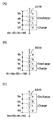
- the top view and sectional drawing explaining the example of a structure of a secondary battery The perspective view explaining the example of a structure of a secondary battery, a top view, and sectional drawing. 8A and 8B illustrate an example of a method for manufacturing a secondary battery. The perspective view explaining the example of a structure of a secondary battery, a top view, and sectional drawing. 8A and 8B illustrate an example of a method for manufacturing a secondary battery. Sectional drawing explaining the example of a structure of a secondary battery. Sectional drawing explaining the conductive support agent etc. which can be used for a secondary battery. Sectional drawing explaining the positive electrode active material which can be used for a secondary battery. The block diagram explaining the battery control unit of an electrical storage apparatus.
- FIG. 10 illustrates an example of an electronic device.
- FIG. 10 illustrates an example of an electronic device.
- FIG. 10 illustrates an example of an electronic device.
- FIG. 10 illustrates an example of an electronic device.
- FIG. 10 illustrates an example of an electronic device.
- 10A and 10B each illustrate an example of an electronic device.
- 10A and 10B each illustrate an example of an electronic device.
- “Electrically connected” includes a case of being connected via “something having an electric action”.
- the “having some electric action” is not particularly limited as long as it can exchange electric signals between the connection targets.
- film and “layer” can be interchanged with each other depending on the case or circumstances.
- conductive layer may be changed to the term “conductive film”.
- insulating film may be changed to the term “insulating layer” in some cases.
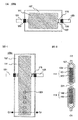
- FIG. 1A is a perspective view of the secondary battery 100
- FIG. 1B is a top view of the secondary battery 100
- FIG. 1C is a cross-sectional view taken along dashed-dotted line A1-A2 in FIGS. 1A and 1B.
- the secondary battery 100 illustrated in FIG. 1 includes a plurality of positive electrodes 111, a positive electrode lead 121 electrically connected to the plurality of positive electrodes 111, a plurality of negative electrodes 115, and a negative electrode lead 125 electrically connected to the plurality of negative electrodes 115.
- Each positive electrode 111 is covered with a separator 103.
- the secondary battery 100 includes an exterior body 107 that covers the plurality of positive electrodes 111, the plurality of negative electrodes 115, and the plurality of separators 103.
- the positive electrode lead 121 and the negative electrode lead 125 have a sealing layer 120.
- the secondary battery 100 has an electrolytic solution 104 in a region covered with the exterior body 107.
- the secondary battery 100 is a secondary battery having a curvature in a uniaxial direction.
- the first electrode 1 includes three positive electrodes 111 each having a positive electrode active material layer 102 formed on one surface of a positive electrode current collector 101 and a negative electrode active material layer 106 formed on one surface of a negative electrode current collector 105.
- three negative electrodes 115 are provided. These electrodes are arranged so that the positive electrode active material layer 102 and the negative electrode active material layer 106 face each other with the separator 103 interposed therebetween.
- the surfaces of the negative electrode 115 on which the negative electrode active material layer 106 is not formed are arranged so as to contact each other.
- a contact surface between the surfaces of the negative electrode 115 not having the negative electrode active material layer 106 that is, a contact surface between metals can be formed.
- the metal-to-metal contact surface can reduce the friction coefficient.
- the secondary battery 100 with high reliability can be obtained.
- the secondary battery 100 in which one or two positive electrodes 111 and 115 are stacked may be used. By reducing the number of stacked layers, the secondary battery 100 can be made thinner and more easily bent. Further, four or more of the positive electrode 111 and the negative electrode 115 may be stacked. By increasing the number of stacked layers, the capacity of the secondary battery 100 can be increased.
- the separator 103 covers the positive electrode 111 in the secondary battery 100 in FIG. 1, the example in which the separator 103 covers the positive electrode 111 is described; however, one embodiment of the present invention is not limited thereto.
- the separator 103 may cover the negative electrode 115. Further, the separator 103 only needs to be provided between the positive electrode active material layer 102 and the negative electrode active material layer 106, and thus the separator 103 may not cover the positive electrode 111 or the negative electrode 115.
- the electrode (positive electrode 111 and negative electrode 115) included in the secondary battery 100 is longer in the bending direction when it is positioned at the outer diameter side than at the inner diameter side of the curve.
- the bending direction herein refers to a direction connecting end portions when the secondary battery is bent as shown in the one-dot broken line A1-A2 in FIG. 1A or in FIG. 5C.
- all the regions of the positive electrode active material layer 102 included in the positive electrode 111 can be disposed to face the negative electrode active material layer 106 included in the negative electrode 115. Therefore, the positive electrode active material included in the positive electrode 111 can be contributed to the battery reaction without waste. Therefore, the capacity per volume of the secondary battery 100 can be increased. This configuration is particularly effective when the curvature of the secondary battery 100 is fixed when the secondary battery 100 is used.
- Adhesion of the outer peripheral portion of the separator 103 may be performed using an adhesive or the like, or may be performed by ultrasonic welding or fusion by heating.
- polypropylene is used as the separator 103, and the outer peripheral portion of the separator 103 is bonded by heating.
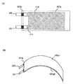
- FIG. 2B shows the bonding portion as a region 103a.
- the separator 103 may be formed so as to cover the positive electrode active material layer 102, and does not need to cover the entire positive electrode 111.
- the separator 103 is bent in FIG. 2A; however, one embodiment of the present invention is not limited to this.
- the positive electrode 111 may be sandwiched between two separators.
- the region 103a may be formed so as to surround most of the four sides.
- the outer peripheral portion of the separator 103 may be bonded intermittently, or may be bonded as dots at regular intervals as shown in FIG.
- adhesion may be performed only on one side of the outer peripheral portion. Or you may join only to 2 sides of an outer peripheral part. Or you may join to 4 sides of an outer peripheral part. Thereby, four sides can be made into an equal state.
- the negative electrode active material layer 106 is formed over the negative electrode current collector 105 and processed into the shape of the negative electrode 115 (FIG. 2C).
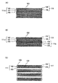
- the positive electrode 111 and the negative electrode 115 are stacked (FIG. 3A).
- three positive electrodes 111 each having a positive electrode active material layer 102 formed on one surface and three negative electrodes 115 each having a negative electrode active material layer 106 formed on one surface are stacked. These are arranged so that the positive electrode active material layer 102 and the negative electrode active material layer 106 face each other with the separator 103 interposed therebetween.
- the surfaces of the negative electrode 115 on which the negative electrode active material layer 106 is not formed are arranged so as to contact each other.
- the positive electrode tabs of the plurality of positive electrode current collectors 101 and the positive electrode lead 121 having the sealing layer 120 are electrically connected by applying ultrasonic waves while applying pressure (ultrasonic welding).
- the lead electrode is likely to be cracked or cut due to stress generated by applying a force from the outside after the power storage unit is manufactured. Therefore, when the positive electrode lead 121 is ultrasonically welded, it may be sandwiched between bonding dies having protrusions, and a curved portion may be formed separately from the connection region on the positive electrode tab. By providing the curved portion, it is possible to relieve stress generated by applying a force from the outside after the secondary battery 100 is manufactured. Therefore, the reliability of the secondary battery 100 can be improved.
- the material of a positive electrode collector shall be strong, such as stainless steel, titanium, etc., and the film thickness of a positive electrode collector shall be secondary by making it 10 micrometers or less.
- a configuration may be adopted in which it is easy to relieve stress generated when an external force is applied from the outside after the battery is manufactured.
- the stress concentration of the positive electrode tab may be reduced by combining a plurality of these.
- the negative electrode tabs of the plurality of negative electrode current collectors 105 and the negative electrode lead 125 including the sealing layer 120 are electrically connected by ultrasonic welding (FIG. 3B).
- the positive electrode and the negative electrode are sandwiched between films and a part is adhered]
- the positive electrode 111 electrically connected by the two films 107a used for the exterior body, more specifically, the film 107a1 which becomes a curved outer diameter side and the film 107a2 which becomes a curved inner diameter side in a later step, respectively.
- the negative electrode 115 are sandwiched (FIG. 3B). Note that although an example in which the two films 107a1 and 107a2 are used for the exterior body is described in this embodiment, one embodiment of the present invention is not limited thereto.
- One package 107a may be bent to sandwich the positive electrode 111 and the negative electrode 115, and sealed in a later process to form the exterior body 107.
- FIG. 4A shows the bonded region as a region 107b.
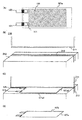
- a sealer 200 for sealing the curved portion of the film 107a will be described.
- a sealer 200 as illustrated in FIG. 5A is preferably used.
- a laminate sealer is a sealer having a function of heating and pressurizing that can adhere a laminate film in which a plastic film is laminated on a metal foil.
- the sealer 200 has an upper first mold 201 and a lower second mold 202.
- Each of the first mold 201 and the second mold 202 has a heater inside.
- the second mold is preferably attached to the base 203.
- the first mold 201 and the second mold 202 are fitted along a desired shape of the secondary battery 100.
- the first mold 201 and the second mold 202 have a curvature, and the curvature of the first mold 201 and the curvature of the second mold 202 are fitted.
- the first mold 201 has an arc-shaped concave portion
- the second mold 202 has an arc-shaped convex portion.
- the sealer 200 may have a curved base on the base 203 that supports the curved shape of the film 107a.
- the film 107a used for the exterior body By sandwiching the film 107a used for the exterior body between the heated first mold 201 and the second mold 202, the film 107a can be thermally welded while being curved.
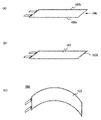
- FIG. 5B shows the curved side of the film 107a.
- FIG. 5C shows the bonded region as a region 107b.
- the other curved side of the film 107a is thermally welded using the sealer 200.
- the film 107a can be bonded while being curved, so that unnecessary stress is not applied to the exterior body 107 of the curved secondary battery 100. Therefore, defects such as cracks and breakage of the exterior body 107 can be suppressed, and the secondary battery 100 with high reliability can be obtained.
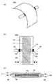
- the electrolytic solution 104 is injected into a region covered with the film 107a from a portion where the film 107a is not bonded (FIG. 6A).
- the secondary battery 100 can be manufactured (FIG. 6B).
- the secondary battery 100 manufactured by the above process is bonded after the film 107a used for the exterior body is curved, and therefore has an outer diameter larger than that of the film 107a2 positioned on the inner diameter side of the secondary battery 100.
- the film 107a1 located on the side is longer in the bending direction.
- FIGS. 2 to 6 illustrate the method of bonding after the film 107a used for the exterior body is curved, one embodiment of the present invention is not limited thereto. It is sufficient that the stress applied to the outer package 107 of the curved secondary battery 100 can be reduced.
- FIG. 1 Another example of a method for manufacturing the secondary battery 100 in FIG. 1 will be described. More specifically, a manufacturing method for bonding one of the films 107a used for the exterior body while heating will be described.
- FIG. 2 and FIG. 3 can be considered about the process of preparing a positive electrode and covering with a separator, the process of preparing a negative electrode, the process of stacking a positive electrode and a negative electrode, and the process of connecting a positive electrode lead and a negative electrode lead.
- a sealer 210 illustrated in FIG. 7B includes an upper bar 211 and a lower bar 212.
- Each of the upper bar 211 and the lower bar 212 has a heater therein.
- the base 213 to which the lower bar 212 is attached also has a heater inside.
- FIG. 7C illustrates the bonded region as a region 107b.
- the other side of the film 107a is thermally welded.
- the one film 107a2 to be heated is a film that becomes the inner diameter side of the curve when it is bent in the subsequent step.
- the film 107a2 used for the exterior body is thermally welded while being heated, the film 107a2 contracts with the cooling after the heat welding. Since the shrinkage of the heated curved inner diameter side film 107a2 is larger than that of the uncured curved outer diameter side film 107a1, the stress generated in the outer package 107 when the secondary battery 100 is curved is increased. Can be reduced.
- the film 107a2 may be bonded in a state where the temperature is higher than that of the film 107a1.
- the film 107a1 and the film 107a2 may be bonded immediately after the film 107a2 is heated by other means.
- the film 107a1 and the film 107a2 may be bonded while cooling the film 107a1 on the outer diameter side of the curve or immediately after cooling.
- the electrolytic solution 104 is injected into a region covered with the film 107a from a portion where the film 107a is not bonded (FIG. 8A).
- FIG. 8B a sealed exterior body 107
- the evacuation may be performed using a degassing sealer, an injection sealer, or the like.
- heating and pressurization can be performed by sandwiching between two heatable bars of the sealer. Each condition can be, for example, 3 seconds at a vacuum degree of 60 kPa, heating at 190 ° C., and pressure at 0.1 MPa.
- the positive electrode and the negative electrode may be pressurized from above the film 107a. By pressurization, bubbles mixed during the electrolyte injection can be excluded from between the positive electrode and the negative electrode.
- the positive electrode 111, the negative electrode 115, and the exterior body 107 are bent into desired shapes. Through the above steps, the curved secondary battery 100 can be manufactured (FIG. 8C).
- the present invention is described in this embodiment. Alternatively, in another embodiment, one embodiment of the present invention will be described. Note that one embodiment of the present invention is not limited thereto.
- the power storage device may be deformed at any time, such as by bending or stretching, or may be fixed in a certain shape. Alternatively, for example, depending on circumstances or conditions, in one embodiment of the present invention, the power storage device may be left uncurved.
- an example in which the present invention is applied to a lithium ion secondary battery has been described.
- one embodiment of the present invention is not limited thereto.
- one embodiment of the present invention includes various secondary batteries, lead storage batteries, lithium ion polymer secondary batteries, nickel / hydrogen storage batteries, nickel / cadmium storage batteries, nickel / iron storage batteries, nickel ⁇ Also applicable to zinc storage battery, silver oxide / zinc storage battery, solid battery, air battery, zinc air battery, primary battery, capacitor, or electric double layer capacitor, ultra capacitor, super capacitor, lithium ion capacitor, etc. Good.
- one embodiment of the present invention may not be applied to a lithium ion secondary battery.
- This embodiment can be implemented in appropriate combination with any of the other embodiments.
- FIG. 9 shows a secondary battery 100a different from FIG.
- FIG. 9A is a perspective view of the secondary battery 100a
- FIG. 9B is a top view of the secondary battery 100a
- FIG. 9C is a cross-sectional view taken along dashed-dotted line B1-B2 in FIG.
- the secondary battery 100a in FIG. 9 is different from the secondary battery 100 in FIG. 1 in the positions of the positive electrode lead 121 and the negative electrode lead 125 and the shapes of the positive electrode 111, the negative electrode 115, and the separator 103.
- the positive electrode lead 121 and the negative electrode lead 125 are drawn out from opposite sides of the exterior body 107. Further, the line connecting the positive electrode lead 121 and the negative electrode lead 125 is not parallel to the curve axis of the secondary battery 100a.
- the tab portion of the positive electrode 111 and the tab portion of the negative electrode 115 which are electrically connected to the positive electrode lead 121 and the negative electrode lead 125, can be provided at locations where the influence of bending is relatively small.
- the tab of the positive electrode 111 and the tab of the negative electrode 115 are thinly elongated, and are thinner than the electrode portion on which the active material is formed, and tend to be weak against bending.
- Embodiment 1 can be referred to for the configuration of the secondary battery 100a other than the positions of the positive electrode lead 121 and the negative electrode lead 125 and the shapes of the positive electrode 111, the negative electrode 115, and the separator 103.
- the manufacturing method described in Embodiment 1 can be referred to.
- FIG. 10A shows a top view of a secondary battery 100b different from FIG.
- the secondary battery 100b in FIG. 10A is different from the secondary battery 100a in FIG. 9 in the shapes of the positive electrode 111, the negative electrode 115, the separator 103, and the exterior body 107.
- the positive electrode 111, the negative electrode 115, the separator 103, and the exterior body 107 of the secondary battery 100b in FIG. 10A are more connected in the direction connecting the tab portion of the positive electrode 111 and the tab portion of the negative electrode 115 than in the direction of the curved axis. long.
- the tab of the positive electrode 111 and the tab of the negative electrode 115 can be provided at a place where the influence of bending is relatively small.
- Embodiment 1 can be referred to for the configuration of the secondary battery 100 b other than the shapes of the positive electrode 111, the negative electrode 115, the separator 103, and the exterior body 107 and the position shapes of the positive electrode lead 121 and the negative electrode lead 125.
- the manufacturing method described in Embodiment 1 can be referred to.
- FIG. 10B and FIG. 10B-2 show a secondary battery 100c different from FIG.
- FIG. 10B-1 is a top view of the secondary battery 100c.
- FIG. 10B-2 is a cross-sectional view taken along one-dot broken line C1-C2 in FIG.
- the secondary battery 100c in FIGS. 10B-1 and 10B-2 has a plurality of holes 221 in the positive electrode 111, the negative electrode 115, the separator 103, and the exterior body 107. Since the secondary battery 100c shown in FIG. 10B-1 and FIG. 10B-2 has a structure having a hole 221, it is also arranged in a band portion of an electronic device that requires a hole, for example, a wristwatch type device. be able to. Therefore, the capacity of the secondary battery 100c can be increased.
- Embodiment 1 can be referred to for the configuration of the secondary battery 100 c other than the shapes of the positive electrode 111, the negative electrode 115, the separator 103, and the exterior body 107 and the position shapes of the positive electrode lead 121 and the negative electrode lead 125.
- the manufacturing method described in Embodiment 1 can be referred to.
- FIG. 11 shows a secondary battery 100d different from FIG.
- FIG. 11A is a perspective view of the secondary battery 100d
- FIG. 11B is a top view of the secondary battery 100d
- FIG. 11C is a cross-sectional view taken along one-dot broken line D1-D2 in FIG. Note that in FIG. 11C, the positive electrode 111, the negative electrode 115, the separator 103, the positive electrode lead 121, the negative electrode lead 125, and the sealing layer 120 are extracted for clarity.
- a secondary battery 100d shown in FIG. 11 is different from the secondary battery 100 of FIG. 1 in that the three sides of the exterior body 107 are sealed by bonding.
- the positions of the positive electrode lead 121 and the negative electrode lead 125 and the shapes of the positive electrode 111, the negative electrode 115, and the separator 103 are also different from those of the secondary battery 100 in FIG.
- the stress applied to the exterior body 107 can be applied by applying the manufacturing method described in Embodiment Mode 1. Can be reduced.
- the negative electrode 115 is placed over the separator 103 (FIG. 12A). At this time, the negative electrode active material layer included in the negative electrode 115 is disposed so as to overlap with the separator 103.
- the separator 103 is bent, and the separator 103 is overlaid on the negative electrode 115.
- the positive electrode 111 is stacked over the separator 103 (FIG. 12B).
- the positive electrode active material layer 102 included in the positive electrode 111 is disposed so as to overlap with the separator 103 and the negative electrode active material layer 106. Note that when an electrode having an active material layer formed on one side of the current collector is used, the positive electrode active material layer 102 of the positive electrode 111 and the negative electrode active material layer 106 of the negative electrode 115 are opposed to each other with the separator 103 interposed therebetween. Deploy.
- the electrode is displaced during the manufacturing process by thermally welding the region where the separators 103 overlap each other and then stacking the next electrode. Can be suppressed. Specifically, it is preferable to thermally weld a region where the separators 103 overlap with each other, for example, a region 103a in FIG. 12B, which does not overlap with the negative electrode 115 or the positive electrode 111.
- the positive electrode 111 and the negative electrode 115 can be stacked with the separator 103 interposed therebetween as shown in FIG.
- a plurality of negative electrodes 115 and a plurality of positive electrodes 111 may be alternately sandwiched between separators 103 that are repeatedly bent in advance.
- the separator 103 covers the plurality of positive electrodes 111 and the plurality of negative electrodes 115.
- a plurality of positive electrodes 111 and a plurality of negative electrodes 115 are bonded by thermally welding a region where separators 103 overlap each other, for example, a region 103b shown in FIG. Cover and bundle with separator 103.
- the plurality of positive electrodes 111, the plurality of negative electrodes 115, and the separator 103 may be bound using a binding material.
- the separator 103 includes a region between the plurality of positive electrodes 111 and the plurality of negative electrodes 115, a plurality of positive electrodes 111, and a plurality of the plurality of positive electrodes 111. And a region arranged so as to cover the negative electrode 115.
- the separator 103 included in the secondary battery 100d in FIG. 11 is one separator that is partially folded. A plurality of positive electrodes 111 and a plurality of negative electrodes 115 are sandwiched between the folded regions of the separator 103.
- the configuration of the secondary battery 100d other than the bonding region of the outer package 107, the shapes of the positive electrode 111, the negative electrode 115, the separator 103, and the outer package 107, and the position shapes of the positive electrode lead 121 and the negative electrode lead 125 are described in the first embodiment. Can be considered.
- the manufacturing method of the secondary battery 100d other than the process of stacking the positive electrode 111 and the negative electrode 115 the manufacturing method described in Embodiment 1 can be referred to.
- FIG. 13 shows a secondary battery 100e different from FIG.
- FIG. 13A is a perspective view of the secondary battery 100e
- FIG. 13B is a top view of the secondary battery 100e
- 13C is a cross-sectional view of the first electrode assembly 130
- FIG. 13C-2 is a cross-sectional view of the second electrode assembly 131
- FIG. 13D is a cross-sectional view taken along one-dot dashed line E1-E2 in FIG. Note that in FIG. 13D, the first electrode assembly 130, the electrode assembly 131, and the separator 103 are extracted and shown for clarity.
- a secondary battery 100e shown in FIG. 13 is different from the secondary battery 100d in FIG. 11 in the arrangement of the positive electrode 111 and the negative electrode 115 and the arrangement of the separator 103.
- the secondary battery 100e includes a plurality of first electrode assemblies 130 and a plurality of electrode assemblies 131.
- the positive electrode 111 a having the positive electrode active material layer 102 on both surfaces of the positive electrode current collector 101, the separator 103, and the negative electrode current collector 105 are both surfaces.
- a negative electrode 115a having a negative electrode active material layer 106, a separator 103, and a positive electrode 111a having a positive electrode active material layer 102 are laminated in this order on both surfaces of the positive electrode current collector 101.
- the negative electrode 115 a having the negative electrode active material layer 106 on both surfaces of the negative electrode current collector 105, the separator 103, and both surfaces of the positive electrode current collector 101 are laminated in this order on both surfaces of the positive electrode current collector 101.
- a positive electrode 111 a having a positive electrode active material layer 102, a separator 103, and a negative electrode 115 a having a negative electrode active material layer 106 on both surfaces of a negative electrode current collector 105 are laminated in this order.
- the plurality of first electrode assemblies 130 and the plurality of electrode assemblies 131 are covered with a rolled separator 103.
- the first electrode assembly 130 is placed over the separator 103 (FIG. 14A).
- the separator 103 is bent, and the separator 103 is overlaid on the first electrode assembly 130.
- two sets of second electrode assemblies 131 are stacked above and below the first electrode assembly 130 with the separator 103 interposed therebetween (FIG. 14B).
- the separator 103 is wound so as to cover the two sets of second electrode assemblies 131. Further, two sets of first electrode assemblies 130 are stacked on the top and bottom of the two sets of second electrode assemblies 131 with the separator 103 interposed therebetween (FIG. 14C).
- the separator 103 is wound so as to cover the two sets of first electrode assemblies 130 (FIG. 14D).
- these electrode assemblies are arranged between the separators 103 wound in a spiral shape.
- the positive electrode 111a of the electrode assembly 130 disposed on the outermost side is not provided with the positive electrode active material layer 102 on the outer side.
- FIG. 13C1 and 13C2 illustrate the structure in which the electrode assembly includes three electrodes and two separators, one embodiment of the present invention is not limited thereto. It is good also as a structure which has 4 or more electrodes and 3 or more separators. By increasing the number of electrodes, the capacity of the secondary battery 100e can be further improved. Alternatively, the structure may include two electrodes and one separator. When there are few electrodes, it can be set as the secondary battery 100e strong against a curve.
- FIG. 13D illustrates a structure in which the secondary battery 100e includes three sets of the first electrode assemblies 130 and two sets of the second electrode assemblies; however, one embodiment of the present invention is not limited thereto. . Furthermore, it is good also as a structure which has many electrode assemblies. By increasing the number of electrode assemblies, the capacity of the secondary battery 100e can be further improved. Moreover, it is good also as a structure which has fewer electrode assemblies. When there are few electrode assemblies, it can be set as the secondary battery 100e strong against a curve.
- FIG. 11 The description of FIG. 11 can be referred to in addition to the arrangement of the positive electrode 111 and the negative electrode 115 and the arrangement of the separator 103 in the secondary battery 100e.
- FIG. 15A illustrates an example of a positive electrode 111 and a negative electrode 115 which are different from those in FIG.
- two positive electrodes 111a each having a positive electrode active material layer 102 are stacked on both surfaces of the positive electrode current collector 101
- four negative electrodes 115 each having a negative electrode active material layer 106 are stacked on one surface of the negative electrode current collector 105.
- a contact surface between the surfaces of the negative electrode 115 that do not have the negative electrode active material layer 106 that is, a contact surface between metals can be formed.
- the capacity per unit volume of the secondary battery 100 can be increased by providing the active material layers on both surfaces of the positive electrode current collector 101a.
- Embodiment 1 can be referred to in addition to the positive electrode 111a and the negative electrode 115, and the stacking order thereof.
- FIG. 15B illustrates an example of a positive electrode 111a and a negative electrode 115a which are different from those in FIG.
- two positive electrodes 111a each having a positive electrode active material layer 102 on both sides of the positive electrode current collector 101
- two negative electrodes 115 each having a negative electrode active material layer 106 on one side of the negative electrode current collector 105
- One negative electrode 115 a having a negative electrode active material layer is stacked on both surfaces of the current collector 105.
- Embodiment 1 can be referred to in addition to the positive electrode 111a, the negative electrode 115, the negative electrode 115a, and the stacking order thereof.
- FIG. 15C illustrates an example of a positive electrode 111 and a negative electrode 115 which are different from those in FIG.
- an electrolytic solution containing a polymer is used as the electrolytic solution 104, and a pair of the positive electrode 111, the negative electrode 115, and the separator 103 are attached to each other with the electrolytic solution 104.
- a large number of metal contact surfaces that is, the surfaces of the positive electrode 111 that do not have the positive electrode active material layer 102 and the surfaces of the negative electrode 115 that do not have the negative electrode active material layer 106 can be formed. Therefore, when the secondary battery 100 is bent, these contact surfaces slip, so that stress caused by the difference between the inner diameter and the outer diameter of the curve can be released.
- the deterioration of the secondary battery 100 can be further suppressed. Further, the secondary battery 100 with higher reliability can be obtained.
- a polymer which the electrolyte solution 104 has in the example of FIG. 15C for example, a polyethylene oxide, polyacrylonitrile, polyvinylidene fluoride, polyacrylate, or polymethacrylate polymer can be used. Further, it is preferable to use a polymer that can gel the electrolyte solution 104 at room temperature (for example, 25 ° C.).
- a polyvinylidene fluoride-based polymer means a polymer containing polyvinylidene fluoride (PVDF), and includes a poly (vinylidene fluoride-hexafluoropropylene) copolymer and the like.
- the polymer can be qualitatively analyzed by using FT-IR (Fourier transform infrared spectrophotometer) or the like.
- FT-IR Fullier transform infrared spectrophotometer
- a polyvinylidene fluoride-based polymer has absorption showing a C—F bond in a spectrum obtained by FT-IR.
- the polyacrylonitrile-based polymer has absorption showing a C ⁇ N bond in the spectrum obtained by FT-IR.
- Embodiment 1 can be referred to in addition to the positive electrode 111, the negative electrode 115, and the stacking order thereof.
- the positive electrode 111 includes a positive electrode current collector 101, a positive electrode active material layer 102 formed on the positive electrode current collector 101, and the like.
- the positive electrode current collector 101 can be formed using a material that has high conductivity and does not elute at the potential of the positive electrode, such as metals such as stainless steel, gold, platinum, aluminum, and titanium, and alloys thereof.
- metals such as stainless steel, gold, platinum, aluminum, and titanium, and alloys thereof.
- an aluminum alloy to which an element that improves heat resistance, such as silicon, titanium, neodymium, scandium, or molybdenum, is added can be used.
- a metal element that forms silicide by reacting with silicon may be used. Examples of metal elements that react with silicon to form silicide include zirconium, titanium, hafnium, vanadium, niobium, tantalum, chromium, molybdenum, tungsten, cobalt, nickel, and the like.
- the positive electrode current collector 101 can have a foil shape, a plate shape (sheet shape), a net shape, a punching metal shape, an expanded metal shape, or the like as appropriate.
- the positive electrode current collector 101 may have a thickness of 5 ⁇ m to 30 ⁇ m.
- an undercoat layer may be provided on the surface of the positive electrode current collector 101 using graphite or the like.
- the positive electrode active material layer 102 includes a binder (binder) for increasing the adhesion of the positive electrode active material, a conductive auxiliary agent for increasing the conductivity of the positive electrode active material layer 102, and the like. Also good.
- Examples of the positive electrode active material used for the positive electrode active material layer 102 include a composite oxide having an olivine crystal structure, a layered rock salt crystal structure, or a spinel crystal structure.
- a compound such as LiFeO 2 , LiCoO 2 , LiNiO 2 , LiMn 2 O 4 , V 2 O 5 , Cr 2 O 5 , or MnO 2 is used.
- LiCoO 2 has the capacity is large, it is stable in the atmosphere as compared to LiNiO 2, because there are advantages such that it is thermally stable than LiNiO 2, preferred.
- a lithium manganese composite oxide that can be represented by a composition formula Li a Mn b McO d
- the element M is preferably a metal element selected from lithium and manganese, or silicon or phosphorus, and more preferably nickel.
- the composition of the metal, silicon, phosphorus, etc. of the entire lithium manganese composite oxide particles can be measured using, for example, ICP-MS (inductively coupled plasma mass spectrometer).
- the composition of oxygen in the entire lithium manganese composite oxide particles can be measured using, for example, EDX (energy dispersive X-ray analysis). Moreover, it can obtain
- the lithium manganese composite oxide means an oxide containing at least lithium and manganese, such as chromium, cobalt, aluminum, nickel, iron, magnesium, molybdenum, zinc, indium, gallium, copper, titanium, niobium, silicon, And at least one element selected from the group consisting of phosphorus and the like.
- a lithium manganese composite oxide having regions having different crystal structures, crystal orientations, or oxygen contents in the surface layer portion and the central portion.
- the composition formula is Li a Mn b Ni c O d (1.6 ⁇ a ⁇ 1.848, 0.19 ⁇ c / b ⁇ 0.935, 2.5 ⁇ d ⁇ 3) is preferable.
- FIG. 16 shows an example of a cross-sectional view of particles of a lithium manganese composite oxide having regions having different crystal structures, crystal orientations, or oxygen contents.
- a lithium-manganese composite oxide having regions with different crystal structures, crystal orientations, or oxygen contents includes a first region 331, a second region 332, and a third region 333. It is preferable to have.
- the second region is in contact with at least a part of the outside of the first region.
- “outside” means closer to the surface of the particle.
- region has an area
- the first region 331 may include a region that is not covered with the second region 332.
- the second region 332 may have a region that is not covered by the third region 333.
- a region where the third region 333 is in contact with the first region 331 may be included.
- the first region 331 may have a region that is not covered by either the second region 332 or the third region 333.
- the second region preferably has a composition different from that of the first region.
- the composition of the first region and the second region is measured separately, the first region has lithium, manganese, element M and oxygen, and the second region has lithium, manganese, element M and oxygen.
- the atomic ratio of lithium, manganese, element M, and oxygen in the first region is expressed as a1: b1: c1: d1, and the number of atoms of lithium, manganese, element M, and oxygen in the second region The case where the ratio is expressed by a2: b2: c2: d2 will be described.
- region can be measured by EDX (energy dispersive X-ray analysis) using TEM (transmission electron microscope), for example.
- d1 / (b1 + c1) is preferably 2.2 or more, more preferably 2.3 or more, and further preferably 2.35 or more and 3 or less.
- D2 / (b2 + c2) is preferably less than 2.2, more preferably less than 2.1, and even more preferably 1.1 or more and 1.9 or less.
- the composition of the entire lithium manganese composite oxide particle including the first region and the second region preferably satisfies the above-described 0.26 ⁇ (b + c) / d ⁇ 0.5.
- the manganese included in the second region may have a valence different from that of the manganese included in the first region.
- the element M included in the second region may have a valence different from that of the element M included in the first region.
- the first region 331 is preferably a lithium manganese composite oxide having a layered rock salt type crystal structure.
- the second region 332 is preferably a lithium manganese composite oxide having a spinel crystal structure.
- the composition and valence of the element when there is a spatial distribution in the composition of each region and the valence of the element, for example, the composition and valence are evaluated for a plurality of locations, the average value is calculated, the composition of the region, It may be a valence.
- a transition layer may be provided between the second region and the first region.
- the transition layer is, for example, a region where the composition changes continuously or stepwise.
- the transition layer is a region where the crystal structure changes continuously or stepwise.
- the transition layer is a region where the lattice constant of the crystal changes continuously or stepwise.
- a mixed layer may be provided between the second region and the first region.
- the mixed layer refers to a case where two or more crystals having different crystal orientations are mixed, for example.
- the mixed layer refers to a case where two or more crystals having different crystal structures are mixed, for example.
- the mixed layer refers to a case where two or more crystals having different compositions are mixed, for example.
- Carbon or a metal compound can be used for the third region.
- the metal include cobalt, aluminum, nickel, iron, manganese, titanium, zinc, and lithium.
- the third region may include an oxide with these metals, a fluoride, or the like.
- the third region particularly preferably has carbon. Since carbon has high conductivity, for example, the resistance of the electrode can be lowered by using particles coated with carbon for the electrode of the storage battery. In addition, since the third region has carbon, the second region in contact with the third region can be oxidized.
- the third region may include graphene, may include graphene oxide, or may include reduced graphene oxide. Graphene and reduced graphene oxide have excellent electrical properties of having high conductivity, and excellent physical properties of high flexibility and mechanical strength. Further, the lithium manganese composite oxide particles can be efficiently coated.
- the cycle characteristics of the secondary battery using the lithium manganese composite oxide as the positive electrode material can be improved.
- the thickness of the layer containing carbon is preferably 0.4 nm or more and 40 nm or less.
- the average particle diameter of primary particles is preferably 5 nm or more and 50 ⁇ m or less, and more preferably 100 nm or more and 500 nm or less. It is preferable specific surface area is less than 5 m 2 / g or more 15 m 2 / g. Moreover, it is preferable that the average particle diameter of a secondary particle is 5 micrometers or more and 50 micrometers or less.
- the average particle diameter can be measured by observation with an SEM (scanning electron microscope) or TEM, a particle size distribution meter using a laser diffraction / scattering method, or the like.
- the specific surface area can be measured by a gas adsorption method.
- a composite material (general formula LiMPO 4 (M is one or more of Fe (II), Mn (II), Co (II), and Ni (II)) can be used as the positive electrode active material.
- Representative examples of the general formula LiMPO 4 include LiFePO 4 , LiNiPO 4 , LiCoPO 4 , LiMnPO 4 , LiFe a Ni b PO 4 , LiFe a Co b PO 4 , LiFe a Mn b PO 4 , LiNi a Co b PO 4 .
- LiNi a Mn b PO 4 (a + b is 1 or less, 0 ⁇ a ⁇ 1, 0 ⁇ b ⁇ 1), LiFe c Ni d Co e PO 4 , LiFe c Ni d M e PO 4 , LiNi c Co d Mn e PO 4 (c + d + e ⁇ 1, 0 ⁇ c ⁇ 1,0 ⁇ d ⁇ 1,0 ⁇ e ⁇ 1), LiFe f Ni g Co h Mn i PO 4 (f + g + h + i is 1 or less, 0 ⁇ f ⁇ 1,0 ⁇ Lithium compounds such as g ⁇ 1, 0 ⁇ h ⁇ 1, 0 ⁇ i ⁇ 1) can be used as the material.
- LiFePO 4 is preferable because it satisfies the requirements for the positive electrode active material in a balanced manner, such as safety, stability, high capacity density, and the presence of lithium ions extracted during initial oxidation (charging).
- a composite material such as a general formula Li (2-j) MSiO 4 (M is one or more of Fe (II), Mn (II), Co (II), Ni (II), 0 ⁇ j ⁇ 2) or the like is used. Can be used.
- Li (2-j) MSiO 4 include Li (2-j) FeSiO 4 , Li (2-j) NiSiO 4 , Li (2-j) CoSiO 4 , Li (2-j) MnSiO 4, Li (2-j) Fe k Ni l SiO 4, Li (2-j) Fe k Co l SiO 4, Li (2-j) Fe k Mn l SiO 4, Li (2-j) Ni k Co l SiO 4, Li (2- j) Ni k Mn l SiO 4 (k + l is 1 or less, 0 ⁇ k ⁇ 1,0 ⁇ l ⁇ 1), Li (2-j) Fe m Ni n Co q SiO 4, Li (2-j) Fe m Ni n Mn q SiO 4, Li (2-j) Ni m Co n Mn q SiO 4 (m + n + q is 1 or less, 0 ⁇ m ⁇ 1,0 ⁇ n ⁇ 1,0 ⁇ q ⁇ 1), Li (2-j) Fe m Ni
- Examples of NASICON type compounds include Fe 2 (MnO 4 ) 3 , Fe 2 (SO 4 ) 3 , and Li 3 Fe 2 (PO 4 ) 3 .
- Oxides, metal chalcogenides such as TiS 2 and MoS 2 (sulfides, selenides, tellurides), oxides having a reverse spinel crystal structure such as LiMVO 4 , vanadium oxides (V 2 O 5 , V 6 O 13 , LiV 3 O 8, etc.), manganese oxides, organic sulfur compounds, and the like can be used.
- carrier ions are alkali metal ions other than lithium ions or alkaline earth metal ions
- an alkali metal for example, sodium or potassium
- an alkaline earth metal for example, Calcium, strontium, barium, beryllium, magnesium, etc.
- a sodium-containing layered oxide such as NaFeO 2 or Na 2/3 [Fe 1/2 Mn 1/2 ] O 2 can be used as the positive electrode active material.
- a conductive material such as a carbon layer may be provided on the surface of the positive electrode active material layer 102.
- a conductive material such as a carbon layer
- the conductivity of the electrode can be improved.
- the coating of the carbon layer on the positive electrode active material layer 102 can be formed by mixing carbohydrates such as glucose at the time of firing the positive electrode active material.
- the average primary particle diameter of the granular positive electrode active material layer 102 may be 50 nm or more and 100 ⁇ m or less.
- a carbon material, a metal material, or a conductive ceramic material can be used.
- a fibrous material as a conductive support agent.
- the content of the conductive additive relative to the total amount of the active material layer is preferably 1 wt% or more and 10 wt% or less, and more preferably 1 wt% or more and 5 wt% or less.
- the conductive assistant can form an electrically conductive network in the electrode.
- the conductive auxiliary agent can maintain the electric conduction path between the positive electrode active materials.
- the conductive assistant for example, artificial graphite such as natural graphite or mesocarbon microbeads, carbon fiber, or the like can be used.
- carbon fibers for example, carbon fibers such as mesophase pitch-based carbon fibers and isotropic pitch-based carbon fibers can be used.
- carbon nanofiber, a carbon nanotube, etc. can be used as carbon fiber.
- Carbon nanotubes can be produced by, for example, a vapor phase growth method.
- the conductive auxiliary agent for example, carbon materials such as carbon black (acetylene black (AB), etc.), graphite (graphite) particles, graphene, fullerene can be used.
- metal powder such as copper, nickel, aluminum, silver, gold, metal fiber, conductive ceramic material, or the like can be used.
- Flaky graphene has excellent electrical properties such as high electrical conductivity, and excellent physical properties such as flexibility and mechanical strength. Therefore, by using graphene as a conductive additive, the contact point and the contact area between the active materials can be increased.
- graphene includes single-layer graphene or multilayer graphene of two to 100 layers.
- Single-layer graphene refers to a sheet of one atomic layer of carbon molecules having a ⁇ bond.
- the graphene oxide refers to a compound obtained by oxidizing the graphene. Note that in the case of reducing graphene oxide to form graphene, all oxygen contained in the graphene oxide is not desorbed and part of oxygen remains in the graphene. In the case where oxygen is contained in graphene, the proportion of oxygen is 2 atomic% or more and 11 atomic% or less, preferably 3 atomic% or more and 10 atomic% or less of the entire graphene as measured by XPS.
- Graphene enables surface contact with low contact resistance, and is extremely conductive even if it is thin, and a conductive path can be efficiently formed in an active material layer even with a small amount.
- an active material having a small average particle diameter for example, an active material having a size of 1 ⁇ m or less is used, the active material has a large specific surface area, and more conductive paths are required to connect the active materials. In such a case, it is particularly preferable to use graphene that has very high conductivity and can efficiently form a conductive path even in a small amount.
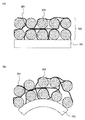
- FIG. 17A is a longitudinal sectional view of the positive electrode active material layer 102 and the positive electrode current collector 101.
- the positive electrode active material layer 102 includes a granular positive electrode active material 322, graphene 321 as a conductive additive, and a binder (also referred to as a binder, not shown).
- the sheet-like graphene 321 is dispersed substantially uniformly inside the positive electrode active material layer 102.
- the graphene 321 is schematically represented by a thick line, but is actually a thin film having a thickness of a single layer or multiple layers of carbon molecules. Since the plurality of graphenes 321 are formed so as to cover or cover the plurality of granular positive electrode active materials 322, or are attached to the surfaces of the plurality of granular positive electrode active materials 322, they are in surface contact with each other. . Further, the graphenes 321 are in surface contact with each other, so that a plurality of graphenes 321 form a three-dimensional electrical conduction network.
- graphene oxide having extremely high dispersibility in a polar solvent is used for forming the graphene 321.
- the dispersion medium is volatilized and removed from the suspension containing uniformly dispersed graphene oxide, and the graphene oxide is reduced to form graphene. Therefore, the graphene 321 remaining in the positive electrode active material layer 102 partially overlaps and is in surface contact with each other. As a result, the electric conduction path is formed.
- the reduction of graphene oxide may be performed by, for example, heat treatment or may be performed using a reducing agent.
- the graphene 321 enables surface contact with low contact resistance, and thus without increasing the amount of the conductive auxiliary agent.
- the electrical conductivity between the positive electrode active material 322 and the graphene 321 can be improved. Therefore, the ratio of the positive electrode active material 322 in the positive electrode active material layer 102 can be increased. Thereby, the discharge capacity of the power storage device can be increased.
- graphene net when graphene is bonded to each other, network graphene (hereinafter referred to as graphene net) can be formed.
- the graphene net When the active material is covered with graphene net, the graphene net can also function as a binder for bonding particles. Therefore, since the amount of the binder can be reduced or not used, the ratio of the active material to the electrode volume and the electrode weight can be improved. That is, the capacity of the power storage device can be increased.
- Such a configuration in which graphene is used as a conductive additive for the positive electrode active material layer or the negative electrode active material layer as described above is particularly effective in a secondary battery having curvature or flexibility.
- FIG. 31A shows a longitudinal sectional view of the positive electrode active material layer 102 and the positive electrode current collector 101 in the case where a particulate conductive auxiliary agent 323 such as acetylene black is used as a conductive auxiliary agent as a conventional example.
- the positive electrode active materials 322 form an electric conduction network by contact with the particulate conductive additive 323.
- FIG. 31B illustrates the case where the positive electrode active material layer 102 and the positive electrode current collector 101 in FIG. 31A are curved.
- a particulate conductive additive 323 is used as the conductive additive as illustrated in FIG. 31B, the distance between the positive electrode active materials 322 changes with the curvature of the positive electrode active material layer 102, and the positive electrode active material 322. There is a risk that a part of the electrical conduction network will be cut off.
- FIG. 17B illustrates the case where the positive electrode active material layer 102 and the positive electrode current collector 101 in FIG. 17A using graphene as a conductive additive are curved. Since graphene is a flexible sheet, an electric conduction network is maintained even when the distance between the positive electrode active materials 322 changes with the curvature of the positive electrode active material layer 102 as shown in FIG. be able to.
- the electrode used for the secondary battery of one embodiment of the present invention can be manufactured by various methods. For example, when an active material layer is formed on a current collector using a coating method, a paste is prepared by mixing an active material, a binder, a conductive additive, and a dispersion medium (also referred to as a solvent). The paste may be applied to vaporize the dispersion medium. Thereafter, if necessary, pressing may be performed by a compression method such as a roll press method or a flat plate press method, and consolidation may be performed.
- a compression method such as a roll press method or a flat plate press method
- the dispersion medium for example, water or an organic solvent having polarity such as N-methylpyrrolidone (NMP) or dimethylformamide can be used. From the viewpoint of safety and cost, it is preferable to use water.
- NMP N-methylpyrrolidone
- dimethylformamide dimethylformamide
- the binder preferably contains a water-soluble polymer.
- polysaccharides can be used as the water-soluble polymer.
- cellulose derivatives such as carboxymethyl cellulose (CMC), methyl cellulose, ethyl cellulose, hydroxypropyl cellulose, diacetyl cellulose, regenerated cellulose, starch, and the like can be used.
- the binder is preferably a rubber material such as styrene-butadiene rubber (SBR), styrene / isoprene / styrene rubber, acrylonitrile / butadiene rubber, butadiene rubber, fluororubber, ethylene / propylene / diene copolymer.
- SBR styrene-butadiene rubber
- styrene / isoprene / styrene rubber acrylonitrile / butadiene rubber, butadiene rubber, fluororubber, ethylene / propylene / diene copolymer.
- polystyrene polymethyl acrylate, polymethyl methacrylate (PMMA), sodium polyacrylate, polyvinyl alcohol (PVA), polyethylene oxide (PEO), polypropylene oxide, polyimide, polyvinyl chloride, polytetrafluoro Use materials such as ethylene, polyethylene, polypropylene, isobutylene, polyethylene terephthalate, nylon, polyvinylidene fluoride (PVdF), polyacrylonitrile (PAN), polyvinyl chloride, ethylene propylene diene polymer, polyvinyl acetate, polymethyl methacrylate, and nitrocellulose. Is preferred.
- the content of the binder with respect to the total amount of the positive electrode active material layer 102 is preferably 1 wt% or more and 10 wt% or less, more preferably 2 wt% or more and 8 wt% or less, and further preferably 3 wt% or more and 5 wt% or less.
- the content of the conductive additive with respect to the total amount of the positive electrode active material layer 102 is preferably 1 wt% or more and 10 wt% or less, and more preferably 1 wt% or more and 5 wt% or less.
- the positive electrode active material layer 102 is formed using a coating method, a positive electrode active material, a binder, and a conductive additive are mixed to prepare a positive electrode paste (slurry), which is applied onto the positive electrode current collector 101 and dried. Just do it.
- the negative electrode 115 includes a negative electrode current collector 105, a negative electrode active material layer 106 formed on the negative electrode current collector 105, and the like.
- the negative electrode current collector 105 a material that has high conductivity and does not alloy with carrier ions such as lithium, such as metals such as stainless steel, gold, platinum, iron, copper, and titanium, and alloys thereof can be used. Alternatively, an aluminum alloy to which an element that improves heat resistance, such as silicon, titanium, neodymium, scandium, or molybdenum, is added can be used.
- the negative electrode current collector 105 can have a foil shape, a plate shape (sheet shape), a net shape, a punching metal shape, an expanded metal shape, or the like as appropriate.
- the negative electrode current collector 105 may have a thickness of 5 ⁇ m to 30 ⁇ m. Further, an undercoat layer may be provided on the surface of the negative electrode current collector 105 using graphite or the like.
- the material of the negative electrode current collector be strong, such as stainless steel or titanium, because the negative electrode current collector can withstand deformation due to expansion of the negative electrode active material layer. This is particularly suitable when a material having a large volume change accompanying charge / discharge, such as a material containing silicon, is used as the negative electrode active material.
- the negative electrode active material layer 106 includes a binder (binder) for increasing the adhesion of the negative electrode active material, a conductive auxiliary agent for increasing the conductivity of the negative electrode active material layer 106, and the like. Also good.
- the binder and the conductive auxiliary material used for the positive electrode active material layer can be referred to for the binder and the conductive auxiliary material used for the negative electrode active material layer.
- the negative electrode active material a material capable of dissolving and precipitating lithium or reversibly reacting with lithium ions can be used, and lithium metal, a carbon-based material, an alloy-based material, and the like can be used.
- Lithium metal is preferable because it has a low redox potential ( ⁇ 3.045 V with respect to the standard hydrogen electrode) and a large specific capacity per weight and volume (3860 mAh / g and 2062 mAh / cm 3 , respectively).
- Examples of the carbon-based material include graphite, graphitizable carbon (soft carbon), non-graphitizable carbon (hard carbon), carbon nanotube, graphene, and carbon black.
- graphite examples include artificial graphite such as mesocarbon microbeads (MCMB), coke-based artificial graphite, and pitch-based artificial graphite, and natural graphite such as spheroidized natural graphite.
- artificial graphite such as mesocarbon microbeads (MCMB)
- coke-based artificial graphite examples include coke-based artificial graphite, and pitch-based artificial graphite, and natural graphite such as spheroidized natural graphite.
- natural graphite such as spheroidized natural graphite.
- Graphite exhibits a potential as low as that of lithium metal (0.1 to 0.3 V vs. Li / Li + ) when lithium ions are inserted into the graphite (when a lithium-graphite intercalation compound is formed). Thereby, a lithium ion secondary battery can show a high operating voltage. Further, graphite is preferable because it has advantages such as relatively high capacity per unit volume, small volume expansion, low cost, and high safety compared to lithium metal.
- an alloy-based material capable of performing a charge / discharge reaction by alloying with a carrier ion or a dealloying reaction can be used as the negative electrode active material.
- the carrier ions are lithium ions
- alloy materials include Mg, Ca, Al, Si, Ge, Sn, Pb, As, Sb, Bi, Ag, Au, Zn, Cd, Hg, and In.
- a material containing at least one of them can be used.
- Such an element has a large capacity with respect to carbon.
- silicon has a theoretical capacity of 4200 mAh / g. For this reason, it is preferable to use silicon for the negative electrode active material.
- alloy materials using such elements include Mg 2 Si, Mg 2 Ge, Mg 2 Sn, SnS 2 , V 2 Sn 3 , FeSn 2 , CoSn 2 , Ni 3 Sn 2 , and Cu 6 Sn 5. , Ag 3 Sn, Ag 3 Sb, Ni 2 MnSb, CeSb 3 , LaSn 3 , La 3 Co 2 Sn 7 , CoSb 3 , InSb, SbSn, and the like.
- the negative electrode active material SiO, SnO, SnO 2, titanium dioxide (TiO 2), lithium titanium oxide (Li 4 Ti 5 O 12) , lithium - graphite intercalation compound (Li x C 6), niobium pentoxide ( An oxide such as Nb 2 O 5 ), tungsten oxide (WO 2 ), or molybdenum oxide (MoO 2 ) can be used.
- SiO refers to a silicon oxide powder containing a silicon-rich portion, and can also be expressed as SiO y (2>y> 0).
- SiO includes a material including one or more selected from Si 2 O 3 , Si 3 O 4 , or Si 2 O, and a mixture of Si powder and silicon dioxide (SiO 2 ).
- SiO may contain other elements (carbon, nitrogen, iron, aluminum, copper, titanium, calcium, manganese, etc.). That is, it refers to a material containing a plurality of materials selected from single crystal Si, amorphous Si, polycrystalline Si, Si 2 O 3 , Si 3 O 4 , Si 2 O, and SiO 2 , and SiO is a colored material.
- SiO x that is not SiO (X is 2 or more), it is colorless and transparent or white and can be distinguished.
- SiO x that is not SiO (X is 2 or more)
- SiO is oxidized by repeating charge and discharge, it may be transformed into SiO 2 .
- Li 2.6 Co 0.4 N 3 shows a large charge / discharge capacity (900 mAh / g, 1890 mAh / cm 3 ) and is preferable.
- the negative electrode active material contains lithium ions, it can be combined with materials such as V 2 O 5 and Cr 3 O 8 that do not contain lithium ions as the positive electrode active material. . Even when a material containing lithium ions is used for the positive electrode active material, lithium and transition metal double nitride can be used as the negative electrode active material by previously desorbing lithium ions contained in the positive electrode active material. .
- a material that causes a conversion reaction can also be used as the negative electrode active material.
- a transition metal oxide that does not undergo an alloying reaction with lithium such as cobalt oxide (CoO), nickel oxide (NiO), or iron oxide (FeO) may be used as the negative electrode active material.
- oxides such as Fe 2 O 3 , CuO, Cu 2 O, RuO 2 and Cr 2 O 3 , sulfides such as CoS 0.89 , NiS and CuS, Zn 3 N 2 are further included.
- nitrides such as Cu 3 N and Ge 3 N 4
- phosphides such as NiP 2 , FeP 2 and CoP 3
- fluorides such as FeF 3 and BiF 3 . Note that since the potential of the fluoride is high, it may be used as a positive electrode active material.
- a negative electrode paste (slurry) is prepared by mixing the negative electrode active material and a binder, and applied to the negative electrode current collector 105 and dried. Good.
- graphene may be formed on the surface of the negative electrode active material layer 106.
- the negative electrode active material is silicon
- the volume change due to the insertion and extraction of carrier ions in the charge / discharge cycle is large, so that the adhesion between the negative electrode current collector 105 and the negative electrode active material layer 106 decreases, and the charge / discharge cycle is reduced. Battery characteristics deteriorate due to discharge. Therefore, when graphene is formed on the surface of the negative electrode active material layer 106 containing silicon, the adhesion between the negative electrode current collector 105 and the negative electrode active material layer 106 is reduced even if the volume of silicon is changed in a charge / discharge cycle. This is preferable because it can be suppressed and deterioration of battery characteristics is reduced.
- a film such as an oxide may be formed on the surface of the negative electrode active material layer 106.
- the film formed by the decomposition of the electrolytic solution during charging cannot release the amount of charge consumed during the formation, and forms an irreversible capacity.
- by providing a film of oxide or the like on the surface of the negative electrode active material layer 106 in advance generation of irreversible capacity can be suppressed or prevented.
- An oxide film containing one and lithium can be used.
- Such a film is a sufficiently dense film as compared with a film formed on the surface of the negative electrode by a conventional decomposition product of the electrolytic solution.
- niobium oxide Nb 2 O 5
- the lithium diffusion coefficient of niobium oxide is 10 ⁇ 9 cm 2 / sec and has high lithium ion conductivity. For this reason, it is possible to permeate
- silicon oxide or aluminum oxide may be used.
- a sol-gel method can be used to form a film that covers the negative electrode active material layer 106.
- the sol-gel method is a method of forming a thin film by baking a solution made of a metal alkoxide, a metal salt, or the like to a gel that has lost fluidity due to a hydrolysis reaction or a polycondensation reaction. Since the sol-gel method is a method of forming a thin film from a liquid phase, raw materials can be homogeneously mixed at a molecular level. For this reason, the active material can be easily dispersed in the gel by adding a negative electrode active material such as graphite to the raw material of the metal oxide film at the solvent stage. In this manner, a film can be formed on the surface of the negative electrode active material layer 106. By using the coating film, it is possible to prevent a reduction in the capacity of the power storage unit.
- a porous insulator such as cellulose, polypropylene (PP), polyethylene (PE), polybutene, nylon, polyester, polysulfone, polyacrylonitrile, polyvinylidene fluoride, and tetrafluoroethylene is used.
- PP polypropylene
- PE polyethylene
- PE polybutene
- nylon polyethylene
- PET polybutene
- nylon polybutene
- nylon polybutene
- polyester polysulfone
- polyvinylidene fluoride and tetrafluoroethylene
- the nonwoven fabrics such as glass fiber, and the diaphragm which compounded glass fiber and polymer fiber.
- Electrolyte As a solvent of the electrolytic solution 104 used for the secondary battery 100, an aprotic organic solvent is preferable.
- security with respect to liquid-leakage property increases by using the polymeric material gelatinized as a solvent of electrolyte solution.
- the secondary battery can be made thinner and lighter.
- Typical examples of the polymer material to be gelated include silicone gel, acrylic gel, acrylonitrile gel, polyethylene oxide gel, polypropylene oxide gel, and fluorine polymer gel.
- the internal temperature increases due to internal short circuit or overcharge of the battery.
- the secondary battery can be prevented from bursting or firing.
- lithium carrier ion e.g. LiPF 6, LiClO 4, LiAsF 6 , LiBF 4, LiAlCl 4, LiSCN, LiBr, LiI, Li 2 SO 4, Li 2 B 10 Cl 10 , Li 2 B 12 Cl 112 , LiCF 3 SO 3 , LiC 4 F 9 SO 3 , LiC (CF 3 SO 2 ) 3 , LiC (C 2 F 5 SO 2 ) 3 , LiN (CF 3 SO 2 ) 2 , lithium salt such as LiN (C 4 F 9 SO 2 ) (CF 3 SO 2 ), LiN (C 2 F 5 SO 2 ) 2 , or two or more of these in any combination and ratio Can be used.
- a lithium carrier ion e.g. LiPF 6, LiClO 4, LiAsF 6 , LiBF 4, LiAlCl 4, LiSCN, LiBr, LiI, Li 2 SO 4, Li 2 B 10 Cl 10 , Li 2 B 12 Cl 112 , LiCF 3 SO 3 , LiC 4 F 9 SO
- the electrolytic solution used for the secondary battery a highly purified electrolytic solution having a small content of elements other than the constituent elements of the granular dust and the electrolytic solution (hereinafter also simply referred to as “impurities”) is used.
- impurities a highly purified electrolytic solution having a small content of elements other than the constituent elements of the granular dust and the electrolytic solution.
- the weight ratio of impurities to the electrolytic solution is preferably 1% or less, preferably 0.1% or less, and more preferably 0.01% or less.
- additives such as vinylene carbonate, to electrolyte solution.
- the film for forming the exterior body 107 includes a metal film (aluminum, stainless steel, nickel steel, etc.), a plastic film made of an organic material, an organic material (organic resin, fiber, etc.), and an inorganic material (ceramic, etc.).
- a single layer film selected from a hybrid material film, a carbon-containing inorganic film (carbon film, graphite film, etc.) or a laminated film composed of a plurality of these films is used.
- the metal film is easy to emboss, and when the embossing is performed to form a concave portion or a convex portion, the surface area of the exterior body 107 that comes into contact with the outside air is increased, so that the heat dissipation effect is excellent.
- the shape of the secondary battery 100 is changed by applying a force from the outside, a bending stress is applied to the exterior body 107 of the secondary battery 100 from the outside, and a part of the exterior body 107 is deformed or partially broken. There is a fear.
- a concave portion or a convex portion in the exterior body 107 distortion caused by the stress applied to the exterior body 107 can be reduced. Therefore, the reliability of the secondary battery 100 can be improved.
- the strain is a measure of deformation indicating the displacement of the material point in the object with respect to the reference (initial state) length of the object.
- FIG. 18 to FIG. 18 illustrate a battery control unit (BMU) that can be used in combination with the secondary battery including the negative electrode described in the above embodiment, and a transistor suitable for a circuit included in the battery control unit.
- BMU battery control unit
- the charge / discharge characteristics vary among the battery cells, and the capacity (output voltage) of each battery cell varies.
- the capacity at the time of overall discharge depends on the battery cells having a small capacity. If there is variation in the capacity of each battery cell, the capacity of the entire battery at the time of discharging becomes small.
- charging is performed with reference to a battery cell having a small capacity, there is a risk of insufficient charging.
- charging is performed with reference to a battery cell having a large capacity, there is a risk of overcharging.
- the battery control unit of the power storage device including the battery cells connected in series has a function of reducing the variation in capacity between the battery cells, which causes insufficient charging and overcharging.
- the circuit configuration for aligning the variation in capacity between battery cells includes a resistance method, a capacitor method, or an inductor method, but here is an example of a circuit configuration that can use a transistor with a small off-current to equalize the variation in capacity. Will be described.
- a transistor including an oxide semiconductor (OS transistor) in a channel formation region is preferable.
- OS transistor oxide semiconductor
- an In-M-Zn oxide (M is Ga, Sn, Y, Zr, La, Ce, or Nd) is used.
- M is Ga, Sn, Y, Zr, La, Ce, or Nd
- x 1 / y 1 is 1/3 or more 6
- z 1 / y 1 is preferably 1/3 or more and 6 or less, more preferably 1 or more and 6 or less. Note that when z 1 / y 1 is greater than or equal to 1 and less than or equal to 6, a CAAC-OS film can be easily formed as the oxide semiconductor film.
- the CAAC-OS film is one of oxide semiconductor films having a plurality of c-axis aligned crystal parts.
- Each layer of metal atoms has a shape reflecting unevenness of a surface (also referred to as a formation surface) or an upper surface on which the CAAC-OS film is formed, and is arranged in parallel with the formation surface or the upper surface of the CAAC-OS film. .
- a peak may appear when the diffraction angle (2 ⁇ ) is around 31 °. Since this peak is attributed to the (009) plane of the InGaZnO 4 crystal, the crystal of the CAAC-OS film has c-axis orientation, and the c-axis is oriented in a direction substantially perpendicular to the formation surface or the top surface. Can be confirmed.
- XRD X-ray diffraction
- CAAC-OS film including an InGaZnO 4 crystal is analyzed by an out-of-plane method, a peak may also appear when 2 ⁇ is around 36 ° in addition to the peak where 2 ⁇ is around 31 °.
- a peak at 2 ⁇ of around 36 ° indicates that a crystal having no c-axis alignment is included in part of the CAAC-OS film.
- the CAAC-OS film preferably has a peak at 2 ⁇ of around 31 ° and no peak at 2 ⁇ of around 36 °.
- the CAAC-OS film is an oxide semiconductor film with a low impurity concentration.
- the impurity is an element other than the main component of the oxide semiconductor film, such as hydrogen, carbon, silicon, or a transition metal element.
- an element such as silicon which has a stronger bonding force with oxygen than the metal element included in the oxide semiconductor film, disturbs the atomic arrangement of the oxide semiconductor film by depriving the oxide semiconductor film of oxygen, and has crystallinity. It becomes a factor to reduce.
- heavy metals such as iron and nickel, argon, carbon dioxide, and the like have large atomic radii (or molecular radii). Therefore, if they are contained inside an oxide semiconductor film, the atomic arrangement of the oxide semiconductor film is disturbed, resulting in crystallinity. It becomes a factor to reduce.
- the impurity contained in the oxide semiconductor film might serve as a carrier trap or a carrier generation source.
- the CAAC-OS film is an oxide semiconductor film with a low density of defect states.
- oxygen vacancies in the oxide semiconductor film can serve as carrier traps or can generate carriers by capturing hydrogen.
- a low impurity concentration and a low density of defect states is called high purity intrinsic or substantially high purity intrinsic.
- a highly purified intrinsic or substantially highly purified intrinsic oxide semiconductor film has few carrier generation sources, and thus can have a low carrier density. Therefore, a transistor including the oxide semiconductor film is unlikely to have electrical characteristics (also referred to as normally-on) in which the threshold voltage is negative.
- a highly purified intrinsic or substantially highly purified intrinsic oxide semiconductor film has few carrier traps. Therefore, a transistor including the oxide semiconductor film has a small change in electrical characteristics and has high reliability. Note that the charge trapped in the carrier trap of the oxide semiconductor film takes a long time to be released, and may behave as if it were a fixed charge. Therefore, a transistor including an oxide semiconductor film with a high impurity concentration and a high density of defect states may have unstable electrical characteristics.
- a transistor including a CAAC-OS film has little variation in electrical characteristics due to irradiation with visible light or ultraviolet light.
- an OS transistor has a larger band gap than a transistor having silicon in a channel formation region (Si transistor), and thus dielectric breakdown is less likely to occur when a high voltage is applied.
- a voltage of several hundred volts is generated.
- the circuit configuration of the battery control unit of the power storage device applied to such a battery cell may be configured by the OS transistor described above. Is suitable.
- FIG. 18 illustrates an example of a block diagram of a power storage device.
- a power storage device BT00 shown in FIG. 18 is connected in series with a terminal pair BT01, a terminal pair BT02, a switching control circuit BT03, a switching circuit BT04, a switching circuit BT05, a transformation control circuit BT06, and a transformation circuit BT07.
- the part can be called a battery control unit.
- the switching control circuit BT03 controls operations of the switching circuit BT04 and the switching circuit BT05. Specifically, the switching control circuit BT03 determines the battery cell (discharge battery cell group) to be discharged and the battery cell (charge battery cell group) to be charged based on the voltage measured for each battery cell BT09.
- the switching control circuit BT03 outputs a control signal S1 and a control signal S2 based on the determined discharge battery cell group and charge battery cell group.
- the control signal S1 is output to the switching circuit BT04.
- This control signal S1 is a signal for controlling the switching circuit BT04 so as to connect the terminal pair BT01 and the discharge battery cell group.
- the control signal S2 is output to the switching circuit BT05.
- This control signal S2 is a signal for controlling the switching circuit BT05 so as to connect the terminal pair BT02 and the rechargeable battery cell group.
- the switching control circuit BT03 is configured between the terminal pair BT01 and the discharge battery cell group or between the terminal pair BT02 and the charging battery cell group based on the configuration of the switching circuit BT04, the switching circuit BT05, and the transformer circuit BT07.
- the control signal S1 and the control signal S2 are generated so that terminals having the same polarity are connected to each other.
- the switching control circuit BT03 measures the voltage for each of the plurality of battery cells BT09. Then, the switching control circuit BT03, for example, sets the battery cell BT09 having a voltage equal to or higher than a predetermined threshold as a high voltage battery cell (high voltage cell) and the battery cell BT09 having a voltage lower than the predetermined threshold as a low voltage battery cell (low voltage). Voltage cell).
- the switching control circuit BT03 determines whether each battery cell BT09 is a high voltage cell or a low voltage cell with reference to the voltage of the battery cell BT09 having the highest voltage or the lowest voltage among the plurality of battery cells BT09. You may judge. In this case, the switching control circuit BT03 determines whether each battery cell BT09 is a high voltage cell or a low voltage cell by determining whether the voltage of each battery cell BT09 is equal to or higher than a predetermined ratio with respect to the reference voltage. Can be judged. Then, the switching control circuit BT03 determines the discharge battery cell group and the charge battery cell group based on the determination result.
- a high voltage cell and a low voltage cell can be mixed in various states.
- the portion where the highest number of high voltage cells are connected in series is the discharge battery cell group.
- the switching control circuit BT03 sets a portion where the most low voltage cells are continuously connected in series as a rechargeable battery cell group.
- the switching control circuit BT03 may preferentially select the battery cell BT09 close to overcharge or overdischarge as the discharge battery cell group or the charge battery cell group.
- FIG. 19 is a diagram for explaining an operation example of the switching control circuit BT03.
- FIG. 19 illustrates an example in which four battery cells BT09 are connected in series.
- the switching control circuit BT03 determines three consecutive high voltage cells a to c as a discharge battery cell group. In addition, the switching control circuit BT03 determines the low voltage cell d as a rechargeable battery cell group.
- the switching control circuit BT03 determines the high voltage cell c as a discharge battery cell group.
- the switching control circuit BT03 preferentially determines the low voltage cell d as a charging battery cell group instead of the two consecutive low voltage cells a and b.
- the switching control circuit BT03 determines the high voltage cell a as a discharge battery cell group.
- the switching control circuit BT03 determines three consecutive low voltage cells b to d as a rechargeable battery cell group.
- the switching control circuit BT03 is a control signal in which information indicating the discharge battery cell group to which the switching circuit BT04 is connected is set based on the results determined as in the examples of FIGS. 19A to 19C.
- the control signal S2 in which information indicating S1 and the rechargeable battery cell group to which the switching circuit BT05 is connected is set is output to the switching circuit BT04 and the switching circuit BT05.
- the switching circuit BT04 sets the connection destination of the terminal pair BT01 to the discharge battery cell group determined by the switching control circuit BT03 according to the control signal S1 output from the switching control circuit BT03.
- the terminal pair BT01 is composed of a pair of terminals A1 and A2.
- the switching circuit BT04 connects either one of the terminals A1 and A2 to the positive terminal of the battery cell BT09 located on the most upstream side (high potential side) in the discharge battery cell group, and the other to the discharge battery cell group.
- the connection destination of the terminal pair BT01 is set by connecting to the negative electrode terminal of the battery cell BT09 located most downstream (low potential side). Note that the switching circuit BT04 can recognize the position of the discharge battery cell group using the information set in the control signal S1.
- the switching circuit BT05 sets the connection destination of the terminal pair BT02 to the rechargeable battery cell group determined by the switching control circuit BT03 according to the control signal S2 output from the switching control circuit BT03.
- the terminal pair BT02 is configured by a pair of terminals B1 and B2.
- the switching circuit BT05 connects either one of the terminals B1 and B2 to the positive terminal of the battery cell BT09 located on the most upstream side (high potential side) in the charging battery cell group, and the other to the charging battery cell group.
- the connection destination of the terminal pair BT02 is set by connecting to the negative electrode terminal of the battery cell BT09 located most downstream (low potential side). Note that the switching circuit BT05 can recognize the position of the rechargeable battery cell group using the information set in the control signal S2.
- 20 and 21 are circuit diagrams showing configuration examples of the switching circuit BT04 and the switching circuit BT05.
- the switching circuit BT04 has a plurality of transistors BT10 and buses BT11 and BT12.
- the bus BT11 is connected to the terminal A1.
- the bus BT12 is connected to the terminal A2.
- One of the sources or drains of the plurality of transistors BT10 is connected to the buses BT11 and BT12 alternately every other one.
- the other of the sources or drains of the plurality of transistors BT10 is connected between two adjacent battery cells BT09.
- the other of the source and the drain of the transistor BT10 located at the uppermost stream is connected to the positive terminal of the battery cell BT09 located at the uppermost stream of the battery unit BT08.
- the other of the source and the drain of the transistor BT10 located on the most downstream side is connected to the negative electrode terminal of the battery cell BT09 located on the most downstream side of the battery unit BT08.
- the switching circuit BT04 is one of the plurality of transistors BT10 connected to the bus BT11 and one of the plurality of transistors BT10 connected to the bus BT12 according to the control signal S1 applied to the gates of the plurality of transistors BT10.
- the discharge battery cell group and the terminal pair BT01 are connected to each other by bringing them into a conductive state.
- the positive electrode terminal of battery cell BT09 located in the most upstream in the discharge battery cell group is connected with either one of terminal A1 or A2 of a terminal pair.
- the negative electrode terminal of battery cell BT09 located in the most downstream in the discharge battery cell group is connected to either the terminal A1 or A2 of the terminal pair, that is, the terminal not connected to the positive electrode terminal.
- An OS transistor is preferably used as the transistor BT10. Since the OS transistor has a small off-state current, it is possible to reduce the amount of charge leaked from a battery cell that does not belong to the discharge battery cell group, and to suppress a decrease in capacity over time. In addition, the OS transistor is unlikely to break down when a high voltage is applied. Therefore, even if the output voltage of the discharge battery cell group is large, the battery cell BT09 connected to the transistor BT10 to be turned off and the terminal pair BT01 can be insulated.
- the switching circuit BT05 includes a plurality of transistors BT13, a current control switch BT14, a bus BT15, and a bus BT16.
- the buses BT15 and BT16 are disposed between the plurality of transistors BT13 and the current control switch BT14.
- One of the sources or drains of the plurality of transistors BT13 is alternately connected to the buses BT15 and BT16 alternately.
- the other of the sources or drains of the plurality of transistors BT13 is connected between two adjacent battery cells BT09.
- the other of the source and the drain of the transistor BT13 located at the uppermost stream is connected to the positive terminal of the battery cell BT09 located at the uppermost stream of the battery unit BT08.
- the other of the source and the drain of the transistor BT13 located on the most downstream side is connected to the negative terminal of the battery cell BT09 located on the most downstream side of the battery unit BT08.
- an OS transistor is preferably used similarly to the transistor BT10. Since the OS transistor has a small off-state current, it is possible to reduce the amount of charge leaked from a battery cell that does not belong to the rechargeable battery cell group, and to suppress a decrease in capacity over time. In addition, the OS transistor is unlikely to break down when a high voltage is applied. Therefore, even if the voltage for charging the charged battery cell group is large, the battery cell BT09 to which the transistor BT13 to be turned off and the terminal pair BT02 can be insulated.
- the current control switch BT14 has a switch pair BT17 and a switch pair BT18. One end of the switch pair BT17 is connected to the terminal B1. The other end of the switch pair BT17 is branched by two switches. One switch is connected to the bus BT15 and the other switch is connected to the bus BT16. One end of the switch pair BT18 is connected to the terminal B2. The other end of the switch pair BT18 is branched by two switches. One switch is connected to the bus BT15 and the other switch is connected to the bus BT16.
- OS transistors are preferably used as in the transistors BT10 and BT13.
- the switching circuit BT05 connects the charging battery cell group and the terminal pair BT02 by controlling the combination of the on / off state of the transistor BT13 and the current control switch BT14 according to the control signal S2.
- the switching circuit BT05 connects the rechargeable battery cell group and the terminal pair BT02 as follows.
- the switching circuit BT05 brings the transistor BT13 connected to the positive terminal of the battery cell BT09 located most upstream in the charging battery cell group into a conductive state in response to the control signal S2 applied to the gates of the plurality of transistors BT13. .
- the switching circuit BT05 conducts the switching transistor BT13 connected to the negative terminal of the battery cell BT09 located most downstream in the charging battery cell group in response to the control signal S2 applied to the gates of the plurality of transistors BT13. Put it in a state.
- the polarity of the voltage applied to the terminal pair BT02 can vary depending on the configuration of the discharge battery cell group connected to the terminal pair BT01 and the transformer circuit BT07. Moreover, in order to flow an electric current in the direction which charges a charging battery cell group, it is necessary to connect terminals of the same polarity between the terminal pair BT02 and the charging battery cell group. Therefore, the current control switch BT14 is controlled to switch the connection destination of the switch pair BT17 and the switch pair BT18 according to the polarity of the voltage applied to the terminal pair BT02 by the control signal S2.
- the switch pair BT17 is controlled to be connected to the positive terminal of the battery cell BT09 by the control signal S2. That is, the switch connected to the bus BT16 of the switch pair BT17 is turned on, and the switch connected to the bus BT15 of the switch pair BT17 is turned off.
- the switch pair BT18 is controlled to be connected to the negative terminal of the battery cell BT09 by the control signal S2.
- the switch connected to the bus BT15 of the switch pair BT18 is turned on, and the switch connected to the bus BT16 of the switch pair BT18 is turned off.
- terminals having the same polarity are connected between the terminal pair BT02 and the rechargeable battery cell group.
- the direction of the electric current which flows from terminal pair BT02 is controlled so that it may become a direction which charges a charging battery cell group.
- the current control switch BT14 may be included in the switching circuit BT04 instead of the switching circuit BT05.
- the polarity of the voltage applied to the terminal pair BT02 is controlled by controlling the polarity of the voltage applied to the terminal pair BT01 in accordance with the current control switch BT14 and the control signal S1.
- the current control switch BT14 controls the direction of current flowing from the terminal pair BT02 to the rechargeable battery cell group.
- FIG. 21 is a circuit diagram showing a configuration example of the switching circuit BT04 and the switching circuit BT05, which is different from FIG.
- the switching circuit BT04 includes a plurality of transistor pairs BT21, a bus BT24, and a bus BT25.
- the bus BT24 is connected to the terminal A1.
- the bus BT25 is connected to the terminal A2.
- One ends of the plurality of transistor pairs BT21 are branched by a transistor BT22 and a transistor BT23, respectively.
- One of the source and the drain of the transistor BT22 is connected to the bus BT24.
- One of the source and the drain of the transistor BT23 is connected to the bus BT25.
- the other ends of the plurality of transistor pairs BT21 are connected between two adjacent battery cells BT09.
- the other end of the transistor pair BT21 located at the most upstream is connected to the positive terminal of the battery cell BT09 located at the most upstream of the battery unit BT08. Moreover, the other end of the transistor pair BT21 located on the most downstream side of the plurality of transistor pairs BT21 is connected to the negative electrode terminal of the battery cell BT09 located on the most downstream side of the battery unit BT08.
- the switching circuit BT04 switches the connection destination of the transistor pair BT21 to either the terminal A1 or the terminal A2 by switching the conduction / non-conduction state of the transistor BT22 and the transistor BT23 according to the control signal S1. Specifically, when the transistor BT22 is in a conductive state, the transistor BT23 is in a nonconductive state, and the connection destination is the terminal A1. On the other hand, when the transistor BT23 is in a conductive state, the transistor BT22 is in a nonconductive state, and the connection destination is the terminal A2. Which of the transistors BT22 and BT23 is turned on is determined by the control signal S1.
- Two transistor pairs BT21 are used to connect the terminal pair BT01 and the discharge battery cell group. Specifically, the connection destination of the two transistor pairs BT21 is determined based on the control signal S1, whereby the discharge battery cell group and the terminal pair BT01 are connected. The connection destinations of the two transistor pairs BT21 are controlled by the control signal S1 so that one is the terminal A1 and the other is the terminal A2.
- the switching circuit BT05 includes a plurality of transistor pairs BT31, a bus BT34, and a bus BT35.
- the bus BT34 is connected to the terminal B1.
- the bus BT35 is connected to the terminal B2.
- One ends of the plurality of transistor pairs BT31 are branched by a transistor BT32 and a transistor BT33, respectively.
- One end branched by the transistor BT32 is connected to the bus BT34.
- One end branched by the transistor BT33 is connected to the bus BT35.
- the other ends of the plurality of transistor pairs BT31 are connected between two adjacent battery cells BT09.
- the other end of the changeover switch pair BT31 located on the uppermost stream is connected to the positive terminal of the battery cell BT09 located on the uppermost stream of the battery unit BT08.
- the other end of the transistor pair BT31 located on the most downstream side of the plurality of transistor pairs BT31 is connected to the negative electrode terminal of the battery cell BT09 located on the most downstream side of the battery unit BT08.
- the switching circuit BT05 switches the connection destination of the transistor pair BT31 to either the terminal B1 or the terminal B2 by switching the conduction / non-conduction state of the transistor BT32 and the transistor BT33 according to the control signal S2. Specifically, when the transistor BT32 is in a conductive state, the transistor BT33 is in a nonconductive state, and the connection destination is the terminal B1. On the other hand, when the transistor BT33 is in a conductive state, the transistor BT32 is in a nonconductive state, and the connection destination is the terminal B2. Which of the transistor BT32 and the transistor BT33 becomes conductive is determined by the control signal S2.
- Two transistor pairs BT31 are used to connect the terminal pair BT02 and the rechargeable battery cell group. Specifically, the connection destination of the two transistor pairs BT31 is determined based on the control signal S2, whereby the rechargeable battery cell group and the terminal pair BT02 are connected. The connection destinations of the two transistor pairs BT31 are controlled by the control signal S2 so that one is the terminal B1 and the other is the terminal B2.
- connection destination of each of the two transistor pairs BT31 is determined by the polarity of the voltage applied to the terminal pair BT02. Specifically, when a voltage is applied to the terminal pair BT02 such that the terminal B1 is a positive electrode and the terminal B2 is a negative electrode, the upstream transistor pair BT31 is in a conductive state and the transistor BT33 is in a nonconductive state. It is controlled by the control signal S2 so as to be in a state. On the other hand, the downstream transistor pair BT31 is controlled by the control signal S2 so that the transistor BT33 is conductive and the transistor BT32 is nonconductive.
- the upstream transistor pair BT31 has the transistor BT33 in a conductive state and the transistor BT32 in a nonconductive state. It is controlled by the control signal S2.
- the transistor pair BT31 on the downstream side is controlled by the control signal S2 so that the transistor BT32 is conductive and the transistor BT33 is nonconductive. In this way, terminals having the same polarity are connected between the terminal pair BT02 and the rechargeable battery cell group. And the direction of the electric current which flows from terminal pair BT02 is controlled so that it may become a direction which charges a charging battery cell group.
- the transformation control circuit BT06 controls the operation of the transformation circuit BT07.
- the transformation control circuit BT06 generates a transformation signal S3 for controlling the operation of the transformation circuit BT07 based on the number of battery cells BT09 included in the discharge battery cell group and the number of battery cells BT09 included in the charge battery cell group. And output to the transformer circuit BT07.
- the transformation control circuit BT06 outputs a transformation signal S3 that controls the transformation circuit BT07 so as to step down the discharge voltage (Vdis) within a range in which the rechargeable battery cell group can be charged.
- the transformation control circuit BT06 outputs a transformation signal S3 that controls the transformation circuit BT07 so as to boost the discharge voltage (Vdis) in a range where an excessive charging voltage is not applied to the charging battery cell group.
- the voltage value used as the excessive charging voltage can be determined in view of the product specifications of the battery cell BT09 used in the battery unit BT08.
- the voltage stepped up and stepped down by the transformer circuit BT07 is applied to the terminal pair BT02 as a charging voltage (Vcha).
- FIGS. 22A to 22C are conceptual diagrams for explaining an operation example of the transformation control circuit BT06 corresponding to the discharge battery cell group and the charge battery cell group described with reference to FIGS. 19A to 19C.
- FIG. 22A to 22C show the battery control unit BT41.
- the battery control unit BT41 includes the terminal pair BT01, the terminal pair BT02, the switching control circuit BT03, the switching circuit BT04, the switching circuit BT05, the transformation control circuit BT06, and the transformation circuit BT07.
- the switching control circuit BT03 determines the high voltage cells a to c as the discharge battery cell group and the low voltage cell d as the charge battery cell group.
- the transformation control circuit BT06 determines the discharge voltage (Vdis) based on the ratio of the number of battery cells BT09 included in the charge battery cell group when the number of battery cells BT09 included in the discharge battery cell group is used as a reference. The conversion ratio N from the charging voltage (Vcha) is calculated.
- the discharge battery is applied as it is to the terminal pair BT02 without being transformed.
- An excessive voltage may be applied to the battery cell BT09 included in the cell group via the terminal pair BT02. Therefore, in the case as shown in FIG. 22A, it is necessary to lower the charging voltage (Vcha) applied to the terminal pair BT02 below the discharging voltage.
- the charging voltage needs to be larger than the total voltage of the battery cells BT09 included in the charging battery cell group. Therefore, the transformation control circuit BT06 sets the conversion ratio N larger than the ratio of the number of battery cells BT09 included in the charged battery cell group when the number of battery cells BT09 included in the discharged battery cell group is used as a reference. To do.
- the transformation control circuit BT06 sets the conversion ratio N to 1 to 10 with respect to the ratio of the number of battery cells BT09 included in the charge battery cell group when the number of battery cells BT09 included in the discharge battery cell group is used as a reference. It is preferable to increase it by about%. At this time, the charging voltage is larger than the voltage of the charging battery cell group, but the charging voltage is actually equal to the voltage of the charging battery cell group. However, in order to make the voltage of the charging battery cell group equal to the charging voltage according to the conversion ratio N, the transformation control circuit BT06 passes a current for charging the charging battery cell group. This current is a value set in the transformation control circuit BT06.
- the number of battery cells BT09 included in the discharge battery cell group is three, and the number of battery cells BT09 included in the charge battery cell group is one.
- BT06 calculates a value slightly larger than 1/3 as the conversion ratio N.
- the transformation control circuit BT06 steps down the discharge voltage according to the conversion ratio N, and outputs a transformation signal S3 that converts it to a charging voltage to the transformation circuit BT07.
- the transformer circuit BT07 applies the charging voltage transformed according to the transformation signal S3 to the terminal pair BT02.
- the battery cell BT09 included in the charging battery cell group is charged by the charging voltage applied to the terminal pair BT02.
- the conversion ratio N is calculated as in FIG.
- the number of battery cells BT09 included in the discharge battery cell group is equal to or less than the number of battery cells BT09 included in the charge battery cell group.
- N is 1 or more. Therefore, in this case, the transformation control circuit BT06 outputs a transformation signal S3 that boosts the discharge voltage and converts it into a charging voltage.
- Transformer circuit BT07 converts the discharge voltage applied to terminal pair BT01 into a charge voltage based on transform signal S3. Then, the transformer circuit BT07 applies the converted charging voltage to the terminal pair BT02.
- the transformer circuit BT07 electrically insulates between the terminal pair BT01 and the terminal pair BT02. Thereby, the transformer circuit BT07 has the absolute voltage of the negative terminal of the battery cell BT09 located most downstream in the discharge battery cell group and the negative terminal of the battery cell BT09 located most downstream in the charge battery cell group. Prevents short circuit due to difference from absolute voltage.
- the transformer circuit BT07 converts the discharge voltage, which is the total voltage of the discharge battery cell group, into a charge voltage based on the transform signal S3.
- the transformer circuit BT07 can use, for example, an insulation type DC (Direct Current) -DC converter.
- the transformation control circuit BT06 controls the charging voltage converted by the transformation circuit BT07 by outputting a signal for controlling the on / off ratio (duty ratio) of the isolated DC-DC converter as the transformation signal S3. .
- Insulated DC-DC converters include flyback method, forward method, RCC (Ringing Choke Converter) method, push-pull method, half-bridge method, and full-bridge method. An appropriate method is selected according to the size.
- FIG. 23 shows the configuration of a transformer circuit BT07 using an insulated DC-DC converter.
- Insulated DC-DC converter BT51 has switch part BT52 and transformer part BT53.
- the switch unit BT52 is a switch that switches on / off the operation of the isolated DC-DC converter, and is realized by using, for example, a MOSFET (Metal-Oxide-Semiconductor Field-Effect Transistor), a bipolar transistor, or the like. Further, the switch unit BT52 periodically switches between the on state and the off state of the isolated DC-DC converter BT51 based on the transform signal S3 that is output from the transform control circuit BT06 and controls the on / off ratio.
- MOSFET Metal-Oxide-Semiconductor Field-Effect Transistor
- the switch unit BT52 can take various configurations depending on the method of the insulation type DC-DC converter used.
- the transformer unit BT53 converts the discharge voltage applied from the terminal pair BT01 into a charge voltage. Specifically, the transformer unit BT53 operates in synchronization with the on / off state of the switch unit BT52, and converts the discharge voltage into a charge voltage according to the on / off ratio. This charging voltage increases as the time for which the on state is turned on is longer in the switching cycle of the switch unit BT52. On the other hand, the charging voltage becomes smaller as the time for which the on state is turned on is shorter in the switching period of the switch unit BT52. In the case of using an insulated DC-DC converter, the terminal pair BT01 and the terminal pair BT02 can be insulated from each other inside the transformer unit BT53.
- FIG. 24 is a flowchart showing a process flow of the power storage device BT00.
- the power storage device BT00 acquires the voltage measured for each of the plurality of battery cells BT09 (step S001). Then, the power storage device BT00 determines whether or not a start condition for the operation of aligning the voltages of the plurality of battery cells BT09 is satisfied (step S002).
- the start condition can be, for example, whether or not the difference between the maximum value and the minimum value of the voltage measured for each of the plurality of battery cells BT09 is equal to or greater than a predetermined threshold. If this start condition is not satisfied (step S002: NO), the voltage of each battery cell BT09 is balanced, and the power storage device BT00 does not perform the subsequent processing.
- step S002 when the start condition is satisfied (step S002: YES), the power storage device BT00 executes a process for aligning the voltages of the battery cells BT09.
- the power storage device BT00 determines whether each battery cell BT09 is a high voltage cell or a low voltage cell based on the measured voltage for each cell (step S003). Then, the power storage device BT00 determines a discharge battery cell group and a charge battery cell group based on the determination result (step S004). Further, power storage device BT00 has a control signal S1 for setting the determined discharge battery cell group as a connection destination of terminal pair BT01, and a control signal S2 for setting the determined charge battery cell group as a connection destination of terminal pair BT02.
- step S005 The power storage device BT00 outputs the generated control signal S1 and control signal S2 to the switching circuit BT04 and the switching circuit BT05, respectively. Then, the switching circuit BT04 connects the terminal pair BT01 and the discharge battery cell group, and the switching circuit BT05 connects the terminal pair BT02 and the discharge battery cell group (step S006).
- the power storage device BT00 generates the transformation signal S3 based on the number of battery cells BT09 included in the discharge battery cell group and the number of battery cells BT09 included in the charge battery cell group (step S007).
- the power storage device BT00 converts the discharge voltage applied to the terminal pair BT01 into a charging voltage based on the transformation signal S3, and applies it to the terminal pair BT02 (step S008). Thereby, the electric charge of the discharge battery cell group is moved to the charge battery cell group.
- the switching circuit BT04 and the switching circuit BT05 can individually switch the battery cells connected to the transformer circuit among the discharge battery cell group and the charge battery cell group.
- the transformer circuit BT07 converts the discharge voltage applied to the terminal pair BT01 based on the number of battery cells BT09 included in the discharge battery cell group and the number of battery cells BT09 group included in the charge battery cell group. And applied to the terminal pair BT02. Thereby, no matter how the discharge-side and charge-side battery cells BT09 are selected, the movement of charges can be realized without any problem.
- the OS transistors for the transistors BT10 and BT13 the amount of charge leaked from the battery cell BT09 that does not belong to the charge battery cell group and the discharge battery cell group can be reduced. Thereby, the fall of the capacity
- the OS transistor has less variation in characteristics with respect to heat than the Si transistor. Thereby, even if the temperature of battery cell BT09 rises, normal operation
- Embodiment 5 (Embodiment 5) In this embodiment, an example in which the secondary battery described in Embodiment 1 is mounted on an electronic device will be described.
- FIG. 25 illustrates an example in which a flexible secondary battery is mounted on an armband type electronic device.
- An armband device 7300 illustrated in FIG. 25 can be attached to the arm 7301 and includes a display portion having a curved surface and a secondary battery that can be bent.
- a display element, a display device that includes a display element, a light-emitting element, and a light-emitting device that includes a light-emitting element can have various modes or have various elements.
- a display element, a display device, a light emitting element, or a light emitting device includes, for example, an EL (electroluminescence) element (an EL element including an organic substance and an inorganic substance, an organic EL element, an inorganic EL element), an LED (white LED, red LED, green LED, Blue LEDs, etc.), transistors (transistors that emit light in response to current), electron-emitting devices, liquid crystal devices, electronic ink, electrophoretic devices, grating light valves (GLV), plasma displays (PDP), MEMS (micro electro mechanical) Display device using system), digital micromirror device (DMD), DMS (digital micro shutter), MIRASOL (registered trademark), IMOD (interference modulation) device, shutter-type
- a display element, a display device, a light-emitting element, or a light-emitting device may include a display medium in which contrast, luminance, reflectance, transmittance, and the like change due to electric or magnetic action.
- An example of a display device using an EL element is an EL display.
- As an example of a display device using an electron-emitting device there is a field emission display (FED), a SED type flat display (SED: Surface-conduction Electron-emitter Display), or the like.
- FED field emission display
- SED SED type flat display
- a display device using a liquid crystal element there is a liquid crystal display (a transmissive liquid crystal display, a transflective liquid crystal display, a reflective liquid crystal display, a direct view liquid crystal display, a projection liquid crystal display) and the like.
- An example of a display device using electronic ink, electronic powder fluid (registered trademark), or an electrophoretic element is electronic paper.
- part or all of the pixel electrode may have a function as a reflective electrode.
- part or all of the pixel electrode may have aluminum, silver, or the like.
- a memory circuit such as an SRAM can be provided under the reflective electrode.
- Graphene or graphite may be a multilayer film in which a plurality of layers are stacked.
- a nitride semiconductor for example, an n-type GaN semiconductor layer having a crystal can be easily formed thereon.
- a p-type GaN semiconductor layer having a crystal or the like can be provided thereon to form an LED.
- an AlN layer may be provided between graphene or graphite and an n-type GaN semiconductor layer having a crystal.
- the GaN semiconductor layer of the LED may be formed by MOCVD.
- the GaN semiconductor layer of the LED can be formed by a sputtering method.
- the armband device 7300 preferably has one or more functional elements.
- a sensor force, displacement, position, velocity, acceleration, angular velocity, number of rotations, distance, light, liquid, magnetism, temperature, chemical substance Those having a function of measuring sound, time, hardness, electric field, current, voltage, power, radiation, flow rate, humidity, gradient, vibration, odor, or infrared can be used.
- functional elements such as a touch panel, an antenna, an electric power generation element, and a speaker.
- the armband type device 7300 is worn on the user's arm at night and the display unit emits light, a traffic safety effect can be obtained.
- a soldier or a guard wears an armband type device 7300 on the upper arm, and while moving forward, receives instructions from the superior in real time and confirms the display displayed on the display section of the new device on the upper arm.
- Military personnel and security guards carry helmets on their heads and have weapons and tools in their hands, making them difficult to use with radios, mobile phones, and devices worn on the head. It is useful for military personnel and guards to wear a new device on the upper arm and to operate the armband type device 7300 by voice input to a voice input unit such as a microphone even when both hands are blocked.
- the armband device 7300 can be usefully used in the sports field. For example, in the case of a marathon or the like, the athlete checks the time with a wristwatch, but it is difficult to check the time unless the arm swings once. If you stop swinging your arms, the rhythm will be disturbed, which may interfere with the competition. Wearing the armband device 7300 on the upper arm allows you to check the time without stopping the swing of the arm, and other information (such as your own location information and your health) Can be displayed.
- the player can operate the new device by voice input without using both hands, ask the coach by the communication function, and the player can confirm the instruction by voice output and display by the voice output unit such as a speaker It is useful to have also.
- an operator wearing a helmet can easily acquire communication and other person's position information so that the armband type device 7300 can be worn on the arm and operated. it can.
- FIG. 26 shows an example in which a flexible secondary battery is mounted on another electronic device.
- a television device also referred to as a television or a television receiver
- a monitor for a computer for example, a computer, a digital camera, a digital video camera, a digital photo frame, a mobile phone
- a large game machine such as a telephone (also referred to as a mobile phone or a mobile phone device), a portable game machine, a portable information terminal, a sound reproducing device, and a pachinko machine.
- a secondary battery having a flexible shape can be incorporated along an inner wall or an outer wall of a house or a building, or along a curved surface of an automobile interior or exterior.
- FIG. 26A illustrates an example of a mobile phone.
- a mobile phone 7400 is provided with a display portion 7402 incorporated in a housing 7401, operation buttons 7403, an external connection port 7404, a speaker 7405, a microphone 7406, and the like. Note that the mobile phone 7400 includes a secondary battery 7407.
- FIG. 26B illustrates a state where the mobile phone 7400 is bent.
- the secondary battery 7407 provided therein is also curved.
- the state of the bent secondary battery 7407 is shown in FIG.
- the secondary battery 7407 is a thin secondary battery.
- the secondary battery 7407 is fixed in a bent state.
- the secondary battery 7407 includes a lead electrode 7408 electrically connected to the current collector. Thereby, the secondary battery 7407 is highly reliable in a bent state.
- FIG. 26D illustrates an example of a bangle display device.
- a portable display device 7100 includes a housing 7101, a display portion 7102, operation buttons 7103, and a secondary battery 7104.
- FIG. 26E shows the state of the secondary battery 7104 bent. When the secondary battery 7104 is bent and attached to the user's arm, the casing is deformed and the curvature of a part or all of the secondary battery 7104 changes. Note that the curvature at a given point of the curve expressed by the value of the radius of the corresponding circle is the curvature radius, and the reciprocal of the curvature radius is called the curvature.
- a part or all of the main surface of the housing or the secondary battery 7104 changes within a radius of curvature of 40 mm or more and 150 mm or less.
- the curvature radius on the main surface of the secondary battery 7104 is in the range of 40 mm to 150 mm, high reliability can be maintained.
- a stove 7500 illustrated in FIG. 26F has a module 7511 attached to a main body 7512, and the module 7511 includes a secondary battery 7501, a motor, a fan, a blower opening 7511a, and a thermoelectric generator.
- the stove 7500 fuel is charged from the opening 7512a and ignited, and then the motor and fan of the module 7511 are rotated using the power of the secondary battery 7501 so that outside air can be sent into the stove 7500 from the blower opening 7511a.
- it can be set as the stove with a strong thermal power.
- cooking can be performed in the upper grill 7513 using the thermal energy obtained for the combustion of the fuel. Further, the thermal energy can be converted into electric power by the thermoelectric generator of the module 7511 and the secondary battery 7501 can be charged. Further, power charged in the secondary battery 7501 can be output from the external terminal 7511b.
- This embodiment can be implemented in appropriate combination with any of the other embodiments.
- Embodiment 6 In this embodiment, another example of an electronic device in which the secondary battery described in Embodiment 1 can be mounted is described.
- FIG. 27A and FIG. 27B illustrate an example of a tablet terminal that can be folded.
- a tablet terminal 9600 illustrated in FIGS. 27A and 27B includes a housing 9630a, a housing 9630b, a movable portion 9640 that connects the housing 9630a and the housing 9630b, a display portion 9631a, and a display portion 9631b.
- a display portion 9631, a display mode switching switch 9626, a power switch 9627, a power saving mode switching switch 9625, a fastener 9629, and an operation switch 9628 are provided.
- FIG. 27A illustrates a state where the tablet terminal 9600 is opened
- FIG. 27B illustrates a state where the tablet terminal 9600 is closed.
- the tablet terminal 9600 includes a secondary battery 9635 inside the housing 9630a and the housing 9630b.
- the secondary battery 9635 is provided across the housing 9630 a and the housing 9630 b through the movable portion 9640.
- Part of the display portion 9631 a can be a touch panel region 9632 a and data can be input when a displayed operation key 9638 is touched.
- a structure in which half of the regions have a display-only function and a structure in which the other half has a touch panel function is shown, but the structure is not limited thereto.
- the entire region of the display portion 9631a may have a touch panel function.
- the entire surface of the display portion 9631a can display keyboard buttons to serve as a touch panel, and the display portion 9631b can be used as a display screen.
- part of the display portion 9631b can be a touch panel region 9632b.
- a keyboard button can be displayed on the display portion 9631b by touching a position where the keyboard display switching button 9539 on the touch panel is displayed with a finger or a stylus.
- Touch input can be performed simultaneously on the touch panel region 9632a and the touch panel region 9632b.
- a display mode switching switch 9626 can switch a display direction such as a vertical display or a horizontal display, and can select a monochrome display or a color display.
- the power saving mode change-over switch 9625 can optimize the display luminance in accordance with the amount of external light in use detected by an optical sensor incorporated in the tablet terminal 9600.
- the tablet terminal may include not only an optical sensor but also other detection devices such as a gyroscope, an acceleration sensor, and other sensors that detect inclination.
- FIG. 27A illustrates an example in which the display areas of the display portion 9631b and the display portion 9631a are the same; however, there is no particular limitation, and one size may differ from the other size, and the display quality may also be high. May be different.
- one display panel may be capable of displaying images with higher definition than the other.
- FIG. 27B shows a closed state, in which the tablet terminal includes a charge / discharge control circuit 9634 including a housing 9630, a solar cell 9633, and a DCDC converter 9636. Further, as the secondary battery 9635, the secondary battery of one embodiment of the present invention is used.
- the tablet terminal 9600 can be folded in two, the housing 9630a and the housing 9630b can be folded so as to overlap when not in use. By folding, the display portion 9631a and the display portion 9631b can be protected; thus, durability of the tablet terminal 9600 can be improved. Further, the secondary battery 9635 using the secondary battery of one embodiment of the present invention has flexibility, and the charge / discharge capacity is unlikely to decrease even when bending and stretching are repeated. Therefore, a tablet terminal with excellent reliability can be provided.
- the tablet terminal shown in FIGS. 27A and 27B has a function for displaying various information (still images, moving images, text images, etc.), a calendar, a date, or a time.
- a function for displaying on the display unit, a touch input function for performing touch input operation or editing of information displayed on the display unit, a function for controlling processing by various software (programs), and the like can be provided.
- Electric power can be supplied to the touch panel, the display unit, the video signal processing unit, or the like by the solar battery 9633 mounted on the surface of the tablet terminal.
- the solar battery 9633 can be provided on one or two surfaces of the housing 9630, and the secondary battery 9635 can be charged efficiently.
- the secondary battery 9635 when the secondary battery of one embodiment of the present invention is used, a reduction in discharge capacity due to repeated charge and discharge can be suppressed; thus, a tablet terminal that can be used for a long time; can do.
- FIG. 27C illustrates the solar battery 9633, the secondary battery 9635, the DCDC converter 9636, the converter 9637, the switches SW1 to SW3, and the display portion 9631.
- the secondary battery 9635, the DCDC converter 9636, the converter 9637, and the switch SW1 to SW3 are portions corresponding to the charge / discharge control circuit 9634 illustrated in FIG.
- the power generated by the solar battery is boosted or lowered by the DCDC converter 9636 so as to be a voltage for charging the secondary battery 9635.
- the switch SW1 is turned on, and the converter 9637 increases or decreases the voltage required for the display portion 9631.
- the secondary battery 9635 may be charged by turning off SW1 and turning on SW2.
- the solar battery 9633 is described as an example of the power generation unit, but is not particularly limited, and the secondary battery 9635 is charged by another power generation unit such as a piezoelectric element (piezo element) or a thermoelectric conversion element (Peltier element). It may be a configuration.
- a non-contact power transmission module that wirelessly (contactlessly) transmits and receives power for charging and other charging means may be combined.
- the secondary battery described in Embodiment 1 can be mounted on a wearable device as shown in FIG.
- the eyeglass-type device 400 can be mounted on an eyeglass-type device 400 as shown in FIG.
- the eyeglass-type device 400 includes a frame 400a and a display unit 400b.
- the secondary battery By mounting the secondary battery on the temple portion of the curved frame 400a, the eyeglass-type device 400 having a good weight balance and a long continuous use time can be obtained.
- the headset type device 401 includes at least a microphone section 401a, a flexible pipe 401b, and an earphone section 401c.
- a secondary battery can be provided in the flexible pipe 401b or the earphone unit 401c.
- a secondary battery 402 b can be provided in the thin housing 402 a of the device 402.
- a secondary battery 403 b can be provided in a thin housing 403 a of the device 403.
- the wristwatch type device 405 includes a display portion 405a and a belt portion 405b, and a secondary battery can be provided in the display portion 405a or the belt portion 405b.
- the belt-type device 406 includes a belt portion 406a and a wireless power feeding / receiving portion 406b, and a secondary battery can be mounted inside the belt portion 406a.
- the secondary battery described in Embodiment 1 can be mounted on a bracelet device 407 as illustrated in FIG.
- the bracelet type device 407 includes two curved secondary batteries 407b in a case 407a.
- a curved display portion 407c is provided on the surface of the case 407a.
- the bracelet type device 407 includes a connecting portion 407d and a hinge portion 407e, and can move up to the connecting portion 407d around the hinge portion 407e.
- charging or the like can be performed through an external terminal provided in the connection portion 407d.
- the secondary battery described in Embodiment 1 can be mounted on the wearable device 410 as illustrated in FIG.
- the wearable device 410 includes a curved secondary battery 412 and a sensor unit 413 in a main body 411.
- the wearable device 410 has the display part 415 and the band part 414, and can be worn on a wrist, for example.
- the display portion that can be used for the display portion 415 the description of the display portion in FIG. 25 can be referred to.
- FIG. 29 illustrates an example of another electronic device.
- a display device 8000 is an example of an electronic device using the secondary battery 8004 according to one embodiment of the present invention.
- the display device 8000 corresponds to a display device for receiving TV broadcasts, and includes a housing 8001, a display portion 8002, a speaker portion 8003, a secondary battery 8004, and the like.
- a secondary battery 8004 according to one embodiment of the present invention is provided in the housing 8001.
- the display device 8000 can receive power from a commercial power supply.
- the display device 8000 can use power stored in the secondary battery 8004.
- the display device 8000 can be used when the secondary battery 8004 according to one embodiment of the present invention is used as an uninterruptible power supply even when power cannot be supplied from a commercial power supply due to a power failure or the like.
- the display portion 8002 includes a liquid crystal display device, a light emitting device including a light emitting element such as an organic EL element, an electrophoretic display device, a DMD (Digital Micromirror Device), a PDP (Plasma Display Panel), and an FED (Field Emission Display).
- a semiconductor display device such as can be used.
- the display device includes all information display devices such as a personal computer and an advertisement display in addition to a TV broadcast reception.
- a stationary lighting device 8100 is an example of an electronic device including the secondary battery 8103 according to one embodiment of the present invention.
- the lighting device 8100 includes a housing 8101, a light source 8102, a secondary battery 8103, and the like.
- FIG. 29 illustrates the case where the secondary battery 8103 is provided inside the ceiling 8104 where the housing 8101 and the light source 8102 are installed.
- the secondary battery 8103 is provided inside the housing 8101. It may be done.
- the lighting device 8100 can receive power from a commercial power supply.
- the lighting device 8100 can use power stored in the secondary battery 8103.
- the lighting device 8100 can be used by using the secondary battery 8103 according to one embodiment of the present invention as an uninterruptible power supply even when power cannot be supplied from a commercial power supply due to a power failure or the like.
- FIG. 29 illustrates a stationary lighting device 8100 provided on the ceiling 8104; however, a secondary battery according to one embodiment of the present invention can be used for a battery other than the ceiling 8104, for example, a side wall 8105, a floor 8106, a window 8107, or the like. It can also be used for a stationary illumination device provided on the desk, or a desktop illumination device.
- the light source 8102 can be an artificial light source that artificially obtains light using electric power.
- discharge lamps such as incandescent bulbs and fluorescent lamps, and light emitting elements such as LEDs and organic EL elements are examples of the artificial light source.
- an air conditioner including an indoor unit 8200 and an outdoor unit 8204 is an example of an electronic device using the secondary battery 8203 according to one embodiment of the present invention.
- the indoor unit 8200 includes a housing 8201, an air outlet 8202, a secondary battery 8203, and the like.
- FIG. 29 illustrates the case where the secondary battery 8203 is provided in the indoor unit 8200, but the secondary battery 8203 may be provided in the outdoor unit 8204. Alternatively, the secondary battery 8203 may be provided in both the indoor unit 8200 and the outdoor unit 8204.
- the air conditioner can receive power from a commercial power supply. Alternatively, the air conditioner can use power stored in the secondary battery 8203.
- the secondary battery 8203 when the secondary battery 8203 is provided in both the indoor unit 8200 and the outdoor unit 8204, the secondary battery 8203 according to one embodiment of the present invention can be used even when electric power cannot be supplied from the commercial power supply due to a power failure or the like.
- an air conditioner By using as an uninterruptible power supply, an air conditioner can be used.
- FIG. 29 illustrates a separate type air conditioner including an indoor unit and an outdoor unit.
- an integrated air conditioner having the functions of the indoor unit and the outdoor unit in one housing is illustrated.
- the secondary battery according to one embodiment of the present invention can also be used.
- an electric refrigerator-freezer 8300 is an example of an electronic device including the secondary battery 8304 according to one embodiment of the present invention.
- the electric refrigerator-freezer 8300 includes a housing 8301, a refrigerator door 8302, a refrigerator door 8303, a secondary battery 8304, and the like.
- the secondary battery 8304 is provided in the housing 8301.
- the electric refrigerator-freezer 8300 can receive power from a commercial power supply.
- the electric refrigerator-freezer 8300 can use power stored in the secondary battery 8304. Therefore, the electric refrigerator-freezer 8300 can be used by using the secondary battery 8304 according to one embodiment of the present invention as an uninterruptible power supply even when electric power cannot be supplied from the commercial power supply due to a power failure or the like.
- This embodiment can be implemented in appropriate combination with any of the other embodiments.
- Embodiment 7 In this embodiment, an example in which the secondary battery described in Embodiment 1 is mounted on a vehicle is shown.
- a next-generation clean energy vehicle such as a hybrid vehicle (HEV), an electric vehicle (EV), or a plug-in hybrid vehicle (PHEV) can be realized.
- HEV hybrid vehicle
- EV electric vehicle
- PHEV plug-in hybrid vehicle
- FIG. 30 illustrates a vehicle using one embodiment of the present invention.
- a car 8400 illustrated in FIG. 30A is an electric car using an electric motor as a power source for traveling. Or it is a hybrid vehicle which can select and use an electric motor and an engine suitably as a motive power source for driving
- the automobile 8400 includes a secondary battery.
- the secondary battery can not only drive an electric motor but also supply power to a light-emitting device such as a headlight 8401 and a room light (not shown).
- the secondary battery can supply power to a display device such as a speedometer or a tachometer included in the automobile 8400.
- the secondary battery can supply power to a semiconductor device such as a navigation system included in the automobile 8400.
- a car 8500 illustrated in FIG. 30B can charge a secondary battery included in the car 8500 by receiving power from an external charging facility by a plug-in method, a non-contact power feeding method, or the like.
- FIG. 30B illustrates a state where charging is performed from the ground-mounted charging device 8021 to the power storage device mounted on the automobile 8500 through the cable 8022.
- the charging method, connector standard, and the like may be appropriately performed by a predetermined method such as CHAdeMO (registered trademark) or a combo.
- the charging device 8021 may be a charging station provided in a commercial facility, or may be a household power source.
- a secondary battery mounted on an automobile 8500 can be charged by an external power supply by plug-in technology. Charging can be performed by converting AC power into DC power via a converter such as an ACDC converter.
- the power receiving device can be mounted on the vehicle, and electric power can be supplied from the ground power transmitting device in a contactless manner and charged.
- charging can be performed not only when the vehicle is stopped but also during traveling by incorporating a power transmission device on a road or an outer wall.
- this non-contact power feeding method may be used to transmit and receive power between vehicles.
- a solar battery may be provided in the exterior part of the vehicle, and the secondary battery may be charged when the vehicle is stopped or traveling.
- An electromagnetic induction method or a magnetic field resonance method can be used for such non-contact power supply.
- the secondary battery mounted in the vehicle can also be used as a power supply source other than the vehicle. In this case, it is possible to avoid using a commercial power source at the peak of power demand.
- This embodiment can be implemented in appropriate combination with any of the other embodiments.
- a lithium manganese composite oxide represented by Li a Mn b Ni c O d was synthesized as a positive electrode active material. Specifically, Li 2 CO 3 , MnCO 3 and NiO were used as starting materials, and Samples A to N represented by Li a Mn b Ni c O d and having different compositions were synthesized.
- Sample A to Sample N A method for manufacturing Sample A to Sample N will be described below. First, the starting materials were weighed for Sample A to Sample N so that the compositions shown in Table 1 were obtained.
- the crushing treatment was performed by adding ethanol and then using a ball mill with a peripheral speed of 12 m / sec and a crushing time of 10 hours.
- samples A to N which are lithium manganese composite oxides having nickel as the positive electrode active material, were obtained.
- electrodes were prepared using the positive electrode active material samples A to N obtained in the above steps, PVdF as a binder, and acetylene black (AB) as a conductive additive.
- PVdF and AB were kneaded with NMP (N-methyl-2-pyrrolidone) which is a polar solvent.
- NMP N-methyl-2-pyrrolidone
- the number of rotations of kneading was 2000 rpm, and the time of kneading was 5 minutes for one time.
- the positive electrode active material was added and kneaded.
- the number of kneading revolutions was 2000 rpm, and the kneading time was 5 times, once for 5 minutes.
- NMP was added and kneaded.
- the number of kneading revolutions was 2000 rpm, and the kneading time was 10 minutes for each kneading, which was repeated twice.
- the said electrode mixture composition was apply
- the composition formula is within the range of Li a Mn b Ni c O d (1.6 ⁇ a ⁇ 1.848, 0.19 ⁇ c / b ⁇ 0.935, 2.5 ⁇ d ⁇ 3). It has been clarified that a lithium manganese composite oxide that exhibits a high capacity can be obtained.
Landscapes
- Chemical & Material Sciences (AREA)
- Chemical Kinetics & Catalysis (AREA)
- Electrochemistry (AREA)
- General Chemical & Material Sciences (AREA)
- Secondary Cells (AREA)
- Sealing Battery Cases Or Jackets (AREA)
- Battery Electrode And Active Subsutance (AREA)
Abstract
二次電池を湾曲させる場合、 最も二次電池の不良の原因になりやすい箇所のひとつとして、 外装体が ある。 湾曲させた二次電池の外装体には、 湾曲の内径と外径で異なる応力がかかり、 亀裂や破断等の 不良が生じやすい。 湾曲した二次電池を作製する際、 二次電池が有する正極、 負極、 外装体用フィルム等の二次電池の構 成要素を、 所望する形状に湾曲してから、 フィルムを接着して二次電池の外装体とする。 または、 平 坦な正極および負極を外装体用フィルムで覆って外装体用フィルムを接着する際、湾曲の内径側にな るフィルムの方が、外径側になるフィルムよりも温度が高い状態で接着する。
Description
本発明は、物、方法、または、製造方法に関する。または、本発明は、プロセス、マシン、マニュファクチャ、または、組成物(コンポジション・オブ・マター)に関する。特に、本発明の一態様は、半導体装置、表示装置、発光装置、蓄電装置、撮像装置、それらの駆動方法、または、それらの製造方法に関する。特に、本発明の一態様は、二次電池および二次電池の作製方法に関する。
近年、ウェアラブルデバイスが盛んに開発されている。ウェアラブルデバイスは身に着けるという性質から、身体の曲面に沿った形状であることが好ましい。そのため、ウェアラブルデバイスに搭載する二次電池も、ディスプレイやそのほかの筐体と同様に、身体の曲面に沿った形状にすることが求められている。
例えば、特許文献1および特許文献2には、湾曲した形状を有する二次電池が開示されている。
湾曲した二次電池の場合、通常、外装体には、アルミニウムラミネートフィルムをはじめとする可撓性を有する材料を用いる。しかしながら、このような二次電池を湾曲させる場合、最も二次電池の不良の原因になりやすい箇所のひとつとして、外装体が挙げられる。湾曲させた二次電池の外装体には、湾曲の内径と外径で異なる応力がかかり、亀裂や破断等の不良が生じやすい。
そのため、本発明の一態様では、新規な構造の二次電池、および該二次電池の作製方法を提供する。具体的には、湾曲を有する新規な構造の二次電池、および該二次電池の作製方法を提供する。
または、本発明の一態様は、新規な蓄電装置、新規な二次電池を搭載した電子機器などを提供することを課題とする。なお、これらの課題の記載は、他の課題の存在を妨げるものではない。なお、本発明の一態様は、必ずしも、これらの課題の全てを解決する必要はない。なお、これら以外の課題は、明細書、図面、請求項などの記載から、自ずと明らかとなるものであり、明細書、図面、請求項などの記載から、これら以外の課題を抽出することが可能である。
上記目的を達成するために、本発明の一態様では、湾曲した二次電池を作製する際、二次電池が有する正極、負極、外装体用フィルム等の二次電池の構成要素を、所望する形状に湾曲してから、フィルムを接着して二次電池の外装体とする。
または、平坦な正極および負極を外装体用フィルムで覆って外装体用フィルムを接着する際、湾曲の内径側になるフィルムの方が、外径側になるフィルムよりも温度が高い状態で接着する。より具体的には、湾曲の内径側になるフィルムを加熱しながら、または加熱した後に接着する。または、湾曲の外径側になるフィルムを冷却しながら、または冷却した後に接着する。
このような工程とすることで、通常の工程で平坦な二次電池を作製してから湾曲させる場合よりも、外装体にかかる応力を減少させることができる。
本発明の一態様は、正極と、負極と、を積層する工程と、正極および負極を、フィルムで覆う工程と、正極、負極およびフィルムを湾曲する工程と、湾曲したフィルム同士を接着することで、フィルムを二次電池の外装体とする工程と、を有する二次電池の作製方法である。
また、本発明の一態様は、正極と、負極と、を積層する工程と、正極および負極を、第1のフィルムおよび第2のフィルムで挟む工程と、第1のフィルムの温度が、第2のフィルムの温度よりも高い状態で、第1のフィルムと、第2のフィルムを接着することで、第1のフィルムおよび第2のフィルムを二次電池の外装体とする工程と、を有する二次電池の作製方法である。
また、本発明の一態様は、上記の作製工程に用いることができる、二次電池の作製のための装置である。より具体的には、上部ヒーターと、下部ヒーターと、を有するラミネートシーラーであって、上部ヒーターは、円弧状の凹部を有し、下部ヒーターは、円弧状の凸部を有し、上部ヒーターと下部ヒーターは嵌合することを特徴とする、ラミネートシーラーである。
新規な構造の二次電池、および該二次電池の作製方法を提供することができる。具体的には、湾曲を有する新規な構造の二次電池、および該二次電池の作製方法を提供することができる。
以下では、本発明の実施の形態について図面を用いて詳細に説明する。ただし、本発明は以下の説明に限定されず、その形態および詳細を様々に変更し得ることは、当業者であれば容易に理解される。また、本発明は以下に示す実施の形態の記載内容に限定して解釈されるものではない。
「電気的に接続」には、「何らかの電気的作用を有するもの」を介して接続されている場合が含まれる。ここで、「何らかの電気的作用を有するもの」は、接続対象間での電気信号の授受を可能とするものであれば、特に制限はない。
図面等において示す各構成の、位置、大きさ、範囲などは、理解を容易にするため、実際の位置、大きさ、範囲などを表していない場合がある。このため、開示する発明は、必ずしも、図面等に開示された位置、大きさ、範囲などに限定されない。
「第1」、「第2」、「第3」などの序数詞は、構成要素の混同を避けるために付すものである。
なお、「膜」という言葉と、「層」という言葉とは、場合によっては、または、状況に応じて、互いに入れ替えることが可能である。例えば、「導電層」という用語を、「導電膜」という用語に変更することが可能な場合がある。または、例えば、「絶縁膜」という用語を、「絶縁層」という用語に変更することが可能な場合がある。
(実施の形態1)
本実施の形態では、図1乃至図8を用いて、本発明の一態様に係る二次電池の構成の例および該二次電池の作製方法の例について説明する。
本実施の形態では、図1乃至図8を用いて、本発明の一態様に係る二次電池の構成の例および該二次電池の作製方法の例について説明する。
[1.代表的な構成]
図1(A)、(B)および(C)に二次電池100の構成の例を示す。図1(A)は二次電池100の斜視図、図1(B)は二次電池100の上面図である。図1(C)は、図1(A)および図1(B)の一点破線A1−A2における断面図である。
図1(A)、(B)および(C)に二次電池100の構成の例を示す。図1(A)は二次電池100の斜視図、図1(B)は二次電池100の上面図である。図1(C)は、図1(A)および図1(B)の一点破線A1−A2における断面図である。
図1に示す二次電池100は、複数の正極111、複数の正極111と電気的に接続された正極リード121、複数の負極115、複数の負極115と電気的に接続された負極リード125を有する。また、正極111はそれぞれ、セパレータ103で覆われている。また二次電池100は、複数の正極111、複数の負極115および複数のセパレータ103を覆う外装体107を有する。また、正極リード121および負極リード125は、封止層120を有する。また二次電池100は、外装体107で覆われた領域に、電解液104を有する。
また図示するように、二次電池100は単軸方向に湾曲を有する二次電池である。
なお、本明細書等において、あるものが湾曲を有するという場合、あるものが、曲がる、凹面を有する、凸面を有する、反る、変形する等と換言することができる。また、そのもの全体にこれらの特徴があることに限られず、少なくとも一部にこれらの特徴があればよい。
なお、図1の二次電池100は、正極集電体101の片面に正極活物質層102が形成された正極111を3枚、負極集電体105の片面に負極活物質層106が形成された負極115を3枚有している。これらの電極を、正極活物質層102と負極活物質層106が、セパレータ103を介して対向するように配置する。また、負極115の負極活物質層106が形成されていない面同士が接するように配置する。
このような配置とすることで、負極115の負極活物質層106を有さない面同士の接触面、つまり金属同士の接触面をつくることができる。金属同士の接触面は、活物質層とセパレータ103との接触面と比較して摩擦係数を小さくすることができる。
そのため、正極111および負極115を湾曲したとき、負極115の負極活物質層106を有さない面同士が滑ることで、湾曲の内径と外径の差により生じる応力を逃がすことができる。そのため、正極111および負極115の劣化を抑制することができる。また、信頼性の高い二次電池100とすることができる。
なお、正極111および負極115を、1枚または2枚ずつ積層した二次電池100としてもよい。積層数を減らすことで、より薄く、湾曲しやすい二次電池100とすることができる。また正極111および負極115を、それぞれ4枚以上積層してもよい。積層数を増やすことで、二次電池100の容量を大きくすることができる。
また、図1の二次電池100ではセパレータ103が正極111を覆う例について説明したが、本発明の一態様はこれに限らない。セパレータ103が負極115を覆う構成としてもよい。またセパレータ103は、正極活物質層102および負極活物質層106の間に設けられればよいため、正極111または負極115を覆わない構成としてもよい。
また、二次電池100が有する電極(正極111および負極115)は、湾曲の内径側に位置するものより、外径側に位置するものの方が、湾曲方向について長いことが好ましい。なお、ここで湾曲方向とは、図1(A)の一点破線A1−A2または図5(C)に示すように、二次電池を湾曲させた際の端部を結ぶ方向を指す。このような構成とすることで、図1(C)に示すように、二次電池100をある曲率で湾曲させた際、正極111および負極115の端部をそろえることができる。すなわち、正極111が有する正極活物質層102のすべての領域を、負極115の有する負極活物質層106と対向して配置することができる。そのため正極111が有する正極活物質を無駄なく電池反応に寄与させることができる。そのため、二次電池100の体積当たりの容量を大きくすることができる。この構成は、二次電池100を使用する際に二次電池100の曲率が固定される場合に特に有効である。
[2.作製方法1]
次に図1の二次電池100の作製方法の一例について説明する。より具体的には、外装体に用いるフィルム107a1およびフィルム107a2を、湾曲させてから接着する作製方法について説明する。
次に図1の二次電池100の作製方法の一例について説明する。より具体的には、外装体に用いるフィルム107a1およびフィルム107a2を、湾曲させてから接着する作製方法について説明する。
[2.1.正極を用意し、セパレータで覆う]
まず、正極集電体101上に正極活物質層102を形成し、正極111の形状に加工する。次いで、折り曲げたセパレータ103で正極111を挟む(図2(A))。
まず、正極集電体101上に正極活物質層102を形成し、正極111の形状に加工する。次いで、折り曲げたセパレータ103で正極111を挟む(図2(A))。
そして正極111の外側の、セパレータ103の外周部分を接着して、袋状のセパレータ103を形成する(図2(B))。セパレータ103の外周部分の接着は、接着材などを用いて行ってもよいし、超音波溶接や、加熱による融着により行ってもよい。
本実施の形態では、セパレータ103としてポリプロピレンを用いて、セパレータ103の外周部分を加熱により接着する。図2(B)に接着部分を、領域103aとして示す。このようにして、正極111をセパレータ103で覆うことができる。セパレータ103は、正極活物質層102を覆うように形成すればよく、正極111の全体を覆う必要は無い。
なお、図2(A)では、セパレータ103を折り曲げているが、本発明の一態様は、これに限定されない。例えば、2枚のセパレータで正極111を挟んで形成してもよい。その場合、領域103aが4辺のほとんどを囲う形で形成されていてもよい。
また、セパレータ103の外周部分の接着は、断続的に行ってもよいし、図2(B)のように一定間隔毎の点状として接着してもよい。
または、外周部分の1辺にのみ、接着を行ってもよい。または、外周部分の2辺にのみ、接合を行ってもよい。または、外周部分の4辺に、接合を行ってもよい。これにより、4辺を均等な状態にすることが出来る。
[2.2.負極を用意する]
次に、負極集電体105上に負極活物質層106を形成し、負極115の形状に加工する(図2(C))。
次に、負極集電体105上に負極活物質層106を形成し、負極115の形状に加工する(図2(C))。
[2.3.正極と負極を積み重ねる]
次に、正極111および負極115を積み重ねる(図3(A))。本実施の形態では、片面に正極活物質層102を形成した正極111を3枚、片面に負極活物質層106を形成した負極115を3枚積層することとする。これらを、正極活物質層102と負極活物質層106が、セパレータ103を介して対向するように配置する。また、負極115の負極活物質層106が形成されていない面同士が接するように配置する。
次に、正極111および負極115を積み重ねる(図3(A))。本実施の形態では、片面に正極活物質層102を形成した正極111を3枚、片面に負極活物質層106を形成した負極115を3枚積層することとする。これらを、正極活物質層102と負極活物質層106が、セパレータ103を介して対向するように配置する。また、負極115の負極活物質層106が形成されていない面同士が接するように配置する。
[2.4.正極リードと負極リードを接続する]
次に、複数の正極集電体101の正極タブと、封止層120を有する正極リード121を、圧力を加えながら超音波を照射して電気的に接続する(超音波溶接)。
次に、複数の正極集電体101の正極タブと、封止層120を有する正極リード121を、圧力を加えながら超音波を照射して電気的に接続する(超音波溶接)。
また、リード電極は、蓄電体の作製後に外から力が加えられて生じる応力により、ヒビや切断が生じやすい。そこで、正極リード121を超音波溶接する際、突起を有するボンディングダイで挟み、正極タブに接続領域は別に湾曲部を形成してもよい。湾曲部を設けることによって、二次電池100の作製後に外から力が加えられて生じる応力を緩和することができる。よって、二次電池100の信頼性を高めることができる。
また、正極タブに湾曲部を形成することに限定されず、正極集電体の材料をステンレス、チタンなどの強度のあるものとし、正極集電体の膜厚を10μm以下とすることで二次電池の作製後に外から外力が加えられ生じる応力を緩和しやすくする構成としてもよい。
勿論、これらを複数組み合わせて正極タブの応力集中を緩和してもよいことは言うまでもない。
そして正極集電体101と同様に、複数の負極集電体105の負極タブと、封止層120を有する負極リード125を超音波溶接により電気的に接続する(図3(B))。
[2.5.正極と負極をフィルムで挟み、一部を接着する]
次に、外装体に用いる2枚のフィルム107a、より詳細には後の工程で湾曲の外径側になるフィルム107a1および湾曲の内径側になるフィルム107a2で、それぞれ電気的に接続された正極111と負極115を挟む(図3(B))。なお、本実施の形態では外装体に2枚のフィルム107a1およびフィルム107a2を用いる例について説明するが、本発明の一態様はこれに限らない。1枚のフィルム107aを折り曲げて正極111と負極115を挟み、後の工程で封止することで外装体107としてもよい。
次に、外装体に用いる2枚のフィルム107a、より詳細には後の工程で湾曲の外径側になるフィルム107a1および湾曲の内径側になるフィルム107a2で、それぞれ電気的に接続された正極111と負極115を挟む(図3(B))。なお、本実施の形態では外装体に2枚のフィルム107a1およびフィルム107a2を用いる例について説明するが、本発明の一態様はこれに限らない。1枚のフィルム107aを折り曲げて正極111と負極115を挟み、後の工程で封止することで外装体107としてもよい。
次に、2枚のフィルム107aの一部、ここでは正極リード121および負極リード125と重畳する一辺を接着する(図4(A))。フィルム107aの接着は、例えば熱溶着により行うことができる。図4(A)に、接着された領域を領域107bとして示す。
[2.6.正極、負極およびフィルムを湾曲させる]
次に、正極111、負極115および外装体に用いるフィルム107a(フィルム107a1およびフィルム107a2)を、所望の形状に湾曲させる(図4(B))。
次に、正極111、負極115および外装体に用いるフィルム107a(フィルム107a1およびフィルム107a2)を、所望の形状に湾曲させる(図4(B))。
[2.7.シーラー]
ここで、フィルム107aの湾曲した部分を封止するための、ラミネートシーラー200について説明する。本発明の一態様の作製方法には、図5(A)に示すようなシーラー200を用いることが好ましい。なお、本明細書等において、ラミネートシーラーとは、金属箔にプラスチックフィルムを積層したラミネートフィルムを接着可能な、加熱および加圧する機能を有するシーラーとする。
ここで、フィルム107aの湾曲した部分を封止するための、ラミネートシーラー200について説明する。本発明の一態様の作製方法には、図5(A)に示すようなシーラー200を用いることが好ましい。なお、本明細書等において、ラミネートシーラーとは、金属箔にプラスチックフィルムを積層したラミネートフィルムを接着可能な、加熱および加圧する機能を有するシーラーとする。
シーラー200は、上部の第1の型201と、下部の第2の型202を有する。第1の型201および第2の型202は、それぞれ内部にヒーターを有する。また第2の型は台203に取り付けられていることが好ましい。第1の型201および第2の型202は、二次電池100の所望の形状に沿って嵌合する。換言すれば、第1の型201と、第2の型202型は湾曲を有し、第1の型201の湾曲と第2の型202の湾曲は嵌合する。例えば図5(A)では、第1の型201が円弧状の凹部を有し、第2の型202が円弧状の凸部を有する。
また、図示していないが、シーラー200は、フィルム107aの湾曲形状を支える湾曲台座を台203上に有していてもよい。
加熱した第1の型201および第2の型202で、外装体に用いるフィルム107aを挟むことで、フィルム107aを、湾曲させたまま熱溶着することができる。
[2.8.フィルムの一部を接着する]
上記のシーラー200を用いて、フィルム107aの湾曲した一辺を熱溶着する(図5(B))。図5(C)に、接着された領域を領域107bとして示す。フィルム107aの湾曲した他の一辺も同様にシーラー200を用いて熱溶着する。
上記のシーラー200を用いて、フィルム107aの湾曲した一辺を熱溶着する(図5(B))。図5(C)に、接着された領域を領域107bとして示す。フィルム107aの湾曲した他の一辺も同様にシーラー200を用いて熱溶着する。
上記のようなシーラー200を用いると、湾曲させたままフィルム107aを接着することができるため、湾曲した二次電池100の外装体107に不要な応力がかからない。そのため外装体107の亀裂や破断等の不良を抑制でき、信頼性の高い二次電池100とすることができる。
[2.9.電解液を注入する]
次に、フィルム107aが接着されていない部分から、フィルム107aで覆われた領域に、電解液104を注入する(図6(A))。
次に、フィルム107aが接着されていない部分から、フィルム107aで覆われた領域に、電解液104を注入する(図6(A))。
[2.10.封止する]
そして真空引きを行いながら、加熱および加圧によりフィルム107aの残りの辺を接着し、封止された外装体107とする。これらの操作は、グローブボックスを用いるなどして酸素や水を排除した環境にて行う。真空引きは、脱気シーラー、注液シーラー等を用いて行うとよい。またシーラーが有する加熱可能な2本のバーで挟むことにより、加熱および加圧を行うことができる。それぞれの条件は、例えば真空度は60kPa、加熱は190℃、加圧は0.1MPaにおいて3秒とすることができる。このとき、フィルム107aの上から正極および負極を加圧してもよい。加圧により、電解液注入の際に混入した気泡を正極と負極の間から排除することができる。
そして真空引きを行いながら、加熱および加圧によりフィルム107aの残りの辺を接着し、封止された外装体107とする。これらの操作は、グローブボックスを用いるなどして酸素や水を排除した環境にて行う。真空引きは、脱気シーラー、注液シーラー等を用いて行うとよい。またシーラーが有する加熱可能な2本のバーで挟むことにより、加熱および加圧を行うことができる。それぞれの条件は、例えば真空度は60kPa、加熱は190℃、加圧は0.1MPaにおいて3秒とすることができる。このとき、フィルム107aの上から正極および負極を加圧してもよい。加圧により、電解液注入の際に混入した気泡を正極と負極の間から排除することができる。
上記の工程で、二次電池100を作製することができる(図6(B))。
なお上記の工程により作製された二次電池100は、外装体に用いるフィルム107aを湾曲させてから接着しているため、二次電池100の湾曲の内径側に位置するフィルム107a2よりも、外径側に位置するフィルム107a1の方が、湾曲方向について長くなる。
[2.11.エージング後、ガス抜きをして再封止する]
なお上記の工程で二次電池100を作製した後、さらにエージングの充放電を行うことが好ましい。さらに、エージングの際に電解液の分解等で生じたガスを抜いてから再封止することがより好ましい。
なお上記の工程で二次電池100を作製した後、さらにエージングの充放電を行うことが好ましい。さらに、エージングの際に電解液の分解等で生じたガスを抜いてから再封止することがより好ましい。
[3.作製方法2]
図2乃至図6では、外装体に用いるフィルム107aを湾曲させてから接着する方法について説明したが、本発明の一態様はこれに限られない。湾曲した二次電池100の外装体107にかかる応力を減少させることができればよい。以下に、図1の二次電池100の作製方法の他の一例について説明する。より具体的には、外装体に用いるフィルム107aの一方を加熱しながら接着する作製方法について説明する。
図2乃至図6では、外装体に用いるフィルム107aを湾曲させてから接着する方法について説明したが、本発明の一態様はこれに限られない。湾曲した二次電池100の外装体107にかかる応力を減少させることができればよい。以下に、図1の二次電池100の作製方法の他の一例について説明する。より具体的には、外装体に用いるフィルム107aの一方を加熱しながら接着する作製方法について説明する。
[3.1.正極および負極を用意し、積み重ね、正極リードおよび負極リードを接続する]
正極を用意しセパレータで覆う工程、負極を用意する工程、正極と負極を積み重ねる工程、および正極リードおよび負極リードを接続する工程については、図2および図3についての記載を参酌することができる。
正極を用意しセパレータで覆う工程、負極を用意する工程、正極と負極を積み重ねる工程、および正極リードおよび負極リードを接続する工程については、図2および図3についての記載を参酌することができる。
[3.2.正極と負極をフィルムで覆い、一部を接着する]
上記工程の後、外装体に用いる2枚のフィルム107aで、それぞれ電気的に接続された正極111と負極115を挟む。次に、2枚のフィルム107aの一部、ここでは正極リード121および負極リード125と重畳する一辺を接着する(図7(A))。
上記工程の後、外装体に用いる2枚のフィルム107aで、それぞれ電気的に接続された正極111と負極115を挟む。次に、2枚のフィルム107aの一部、ここでは正極リード121および負極リード125と重畳する一辺を接着する(図7(A))。
[3.3.シーラー]
ここで、外装体に用いるフィルム107aの一方を加熱しながら接着するためのラミネートシーラー210について説明する。
ここで、外装体に用いるフィルム107aの一方を加熱しながら接着するためのラミネートシーラー210について説明する。
図7(B)に示すシーラー210は、上部のバー211と、下部のバー212を有する。上部のバー211および下部のバー212は、それぞれ内部にヒーターを有する。また下部のバー212が取り付けられている台213も、内部にヒーターを有する。
[3.4.フィルムの一部を接着する]
上記のシーラー210を用いて、フィルム107a2を台213で加熱しながら、フィルム107aの一辺を熱溶着する(図7(C))。図7(D)に、接着された領域を領域107bとして示す。フィルム107aの他の一辺も同様に熱溶着する。この工程において、加熱する一方のフィルム107a2は、後の工程で湾曲した際に湾曲の内径側になるフィルムである。
上記のシーラー210を用いて、フィルム107a2を台213で加熱しながら、フィルム107aの一辺を熱溶着する(図7(C))。図7(D)に、接着された領域を領域107bとして示す。フィルム107aの他の一辺も同様に熱溶着する。この工程において、加熱する一方のフィルム107a2は、後の工程で湾曲した際に湾曲の内径側になるフィルムである。
外装体に用いるフィルム107a2を加熱しながら熱溶着するため、熱溶着後、冷却に伴って、フィルム107a2に収縮が生じる。加熱しなかった湾曲の外径側のフィルム107a1よりも、加熱した湾曲の内径側のフィルム107a2の収縮がより大きくなるため、二次電池100を湾曲させた際に、外装体107に生じる応力を減少させることができる。
なお、上記ではフィルム107a2を加熱する方法について説明したが、本発明の一態様はこれに限らない。フィルム107a2の方が、フィルム107a1よりも温度が高い状態で接着されればよい。
そのため、フィルム107a2を他の手段で加熱した後、すぐにフィルム107a1とフィルム107a2を接着してもよい。また、湾曲の外径側のフィルム107a1を冷却しながら、または冷却した後すぐにフィルム107a1とフィルム107a2を接着してもよい。
[3.5.電解液を注入する]
次に、フィルム107aが接着されていない部分から、フィルム107aで覆われた領域に、電解液104を注入する(図8(A))。
次に、フィルム107aが接着されていない部分から、フィルム107aで覆われた領域に、電解液104を注入する(図8(A))。
[3.6.封止する]
そして真空引きを行いながら、加熱および加圧によりフィルム107aの残りの辺を接着し、封止された外装体107とする(図8(B))。これらの操作は、グローブボックスを用いるなどして酸素や水を排除した環境にて行う。真空引きは、脱気シーラー、注液シーラー等を用いて行うとよい。またシーラーが有する加熱可能な2本のバーで挟むことにより、加熱および加圧を行うことができる。それぞれの条件は、例えば真空度は60kPa、加熱は190℃、加圧は0.1MPaにおいて3秒とすることができる。このとき、フィルム107aの上から正極および負極を加圧してもよい。加圧により、電解液注入の際に混入した気泡を正極と負極の間から排除することができる。
そして真空引きを行いながら、加熱および加圧によりフィルム107aの残りの辺を接着し、封止された外装体107とする(図8(B))。これらの操作は、グローブボックスを用いるなどして酸素や水を排除した環境にて行う。真空引きは、脱気シーラー、注液シーラー等を用いて行うとよい。またシーラーが有する加熱可能な2本のバーで挟むことにより、加熱および加圧を行うことができる。それぞれの条件は、例えば真空度は60kPa、加熱は190℃、加圧は0.1MPaにおいて3秒とすることができる。このとき、フィルム107aの上から正極および負極を加圧してもよい。加圧により、電解液注入の際に混入した気泡を正極と負極の間から排除することができる。
[3.7.湾曲する]
次に、正極111、負極115および外装体107を所望の形状に湾曲する。上記の工程で、湾曲した二次電池100を作製することができる(図8(C))。
次に、正極111、負極115および外装体107を所望の形状に湾曲する。上記の工程で、湾曲した二次電池100を作製することができる(図8(C))。
[3.8.エージング後、ガス抜きをして再封止する]
なお上記の工程で二次電池100を作製した後、さらにエージングの充放電を行うことが好ましい。さらに、エージングの際に電解液の分解等で生じたガスを抜いてから再封止することがより好ましい。
なお上記の工程で二次電池100を作製した後、さらにエージングの充放電を行うことが好ましい。さらに、エージングの際に電解液の分解等で生じたガスを抜いてから再封止することがより好ましい。
なお、本実施の形態において、本発明の一態様について述べた。または、他の実施の形態において、本発明の一態様について述べる。ただし、本発明の一態様は、これらに限定されない。例えば、本発明の一態様として、湾曲した二次電池について示したが、本発明の一態様はこれに限定されない。場合によっては、または、状況に応じて、本発明の一態様では、蓄電装置を、曲げる、伸ばす等、随時変形してもよいし、何らかの形状のままに固定してもよい。または例えば、場合によっては、または、状況に応じて、本発明の一態様では、蓄電装置を、湾曲させないままの状態としてもよい。例えば、本発明の一態様として、リチウムイオン二次電池に適用した場合の例を示したが、本発明の一態様は、これに限定されない。場合によっては、または、状況に応じて、本発明の一態様は、様々な二次電池、鉛蓄電池、リチウムイオンポリマー二次電池、ニッケル・水素蓄電池、ニッケル・カドミウム蓄電池、ニッケル・鉄蓄電池、ニッケル・亜鉛蓄電池、酸化銀・亜鉛蓄電池、固体電池、空気電池、亜鉛空気電池、一次電池、キャパシタ、または、電気二重層キャパシタ、ウルトラ・キャパシタ、スーパー・キャパシタ、リチウムイオンキャパシタ、などに適用してもよい。または例えば、場合によっては、または、状況に応じて、本発明の一態様は、リチウムイオン二次電池に適用しなくてもよい。
本実施の形態は、他の実施の形態と適宜組み合わせて実施することが可能である。
(実施の形態2)
本実施の形態では、図9乃至図15を用いて、本発明の一態様の二次電池の変形例について説明する。
本実施の形態では、図9乃至図15を用いて、本発明の一態様の二次電池の変形例について説明する。
[1.変形例1]
図9に、図1と異なる二次電池100aを示す。図9(A)は二次電池100aの斜視図、図9(B)は二次電池100aの上面図である。図9(C)は、図9(B)における一点破線B1−B2における断面図である。
図9に、図1と異なる二次電池100aを示す。図9(A)は二次電池100aの斜視図、図9(B)は二次電池100aの上面図である。図9(C)は、図9(B)における一点破線B1−B2における断面図である。
図9の二次電池100aは、正極リード121および負極リード125の位置、および正極111、負極115およびセパレータ103の形状が、図1の二次電池100と異なる。
図9の二次電池100aでは、正極リード121および負極リード125が、それぞれ外装体107の対向する辺から引き出されている。また、正極リード121および負極リード125を結んだ線は、二次電池100aの湾曲の軸と平行にならない。このような構成とすることで、正極リード121および負極リード125と電気的に接続される、正極111のタブ部分および負極115のタブ部分を、湾曲の影響の比較的少ない箇所に設けることができる。正極111のタブおよび負極115のタブは、細く伸びた形状であり、また活物質が形成された電極部に比べて薄く、湾曲に弱くなりがちである。正極111のタブおよび負極115のタブを、湾曲の影響の少ない箇所に設けることで、より信頼性の高い二次電池100aとすることができる。
二次電池100aの、正極リード121および負極リード125の位置、および正極111、負極115およびセパレータ103の形状以外の構成は、実施の形態1の記載を参酌することができる。また図9の二次電池100aの作製方法は、実施の形態1に記載の作製方法を参酌することができる。
[2.変形例2]
図10(A)に、図9と異なる二次電池100bの上面図を示す。
図10(A)に、図9と異なる二次電池100bの上面図を示す。
図10(A)の二次電池100bは、正極111、負極115、セパレータ103および外装体107の形状が図9の二次電池100aと異なる。図10(A)の二次電池100bの正極111、負極115、セパレータ103および外装体107は、湾曲の軸の方向よりも、正極111のタブ部分と負極115のタブ部分を結ぶ方向の方が長い。このような構造の二次電池100bとしても、正極111のタブおよび負極115のタブを、湾曲の影響が比較的少ない箇所に設けることができる。
二次電池100bの、正極111、負極115、セパレータ103および外装体107の形状、正極リード121および負極リード125の位置形状以外の構成は、実施の形態1の記載を参酌することができる。また図10(A)の二次電池100bの作製方法は、実施の形態1に記載の作製方法を参酌することができる。
[3.変形例3]
図10(B)−1および図10(B)−2に、図9と異なる二次電池100cを示す。図10(B)−1は二次電池100cの上面図である。図10(B)−2は、図10(B)−1の一点破線C1−C2における断面図である。
図10(B)−1および図10(B)−2に、図9と異なる二次電池100cを示す。図10(B)−1は二次電池100cの上面図である。図10(B)−2は、図10(B)−1の一点破線C1−C2における断面図である。
図10(B)−1および図10(B)−2の二次電池100cは、正極111、負極115、セパレータ103および外装体107に、複数の穴221を有する。図10(B)−1および図10(B)−2に示す二次電池100cは、穴221を有する構成であるため、穴が必要な電子デバイス、例えば腕時計型デバイスのバンド部分にも配置することができる。そのため二次電池100cの容量を大きくすることができる。
二次電池100cの、正極111、負極115、セパレータ103および外装体107の形状、正極リード121および負極リード125の位置形状以外の構成は、実施の形態1の記載を参酌することができる。また二次電池100cの作製方法は、実施の形態1に記載の作製方法を参酌することができる。
[4.変形例4]
図11に、図9と異なる二次電池100dを示す。図11(A)は二次電池100dの斜視図、図11(B)は二次電池100dの上面図である。図11(C)は、図11(B)の一点破線D1−D2における断面図である。なお、図11(C)では図を明瞭にするため、正極111、負極115、セパレータ103、正極リード121、負極リード125、および封止層120を抜粋して示す。
図11に、図9と異なる二次電池100dを示す。図11(A)は二次電池100dの斜視図、図11(B)は二次電池100dの上面図である。図11(C)は、図11(B)の一点破線D1−D2における断面図である。なお、図11(C)では図を明瞭にするため、正極111、負極115、セパレータ103、正極リード121、負極リード125、および封止層120を抜粋して示す。
図11に示す二次電池100dは、外装体107の3辺を接着することで封止している点で、図1の二次電池100と異なる。また正極リード121および負極リード125の位置、および正極111、負極115およびセパレータ103の形状も、図1の二次電池100と異なる。
図11に示す二次電池100dのように、外装体107の3辺を接着することで封止する場合でも、実施の形態1で説明した作製方法を適用することで、外装体107にかかる応力を軽減することができる。
ここで図12を用いて、図11に示す二次電池100dの作製方法の一部について説明する。
まずセパレータ103上に、負極115を配置する(図12(A))。このとき、負極115が有する負極活物質層が、セパレータ103と重畳するように配置する。
次に、セパレータ103を折り曲げ、負極115の上にセパレータ103を重ねる。次に、セパレータ103の上に、正極111を重ねる(図12(B))。このとき、正極111が有する正極活物質層102が、セパレータ103および負極活物質層106と重畳するように配置する。なお、集電体の片面に活物質層が形成されている電極を用いる場合は、正極111の正極活物質層102と、負極115の負極活物質層106がセパレータ103を介して対向するように配置する。
セパレータ103にポリプロピレン等の熱溶着が可能な材料を用いている場合は、セパレータ103同士が重畳している領域を熱溶着してから次の電極を重ねることで、作製工程中に電極がずれることを抑制できる。具体的には、負極115または正極111と重畳しておらず、セパレータ103同士が重畳している領域、たとえば図12(B)の領域103aで示す領域を熱溶着することが好ましい。
この工程を繰り返すことで、図12(C)に示すように、セパレータ103を挟んで正極111および負極115を積み重ねることができる。
なお、あらかじめ繰り返し折り曲げたセパレータ103に、複数の負極115および複数の正極111を交互に挟むように配置してもよい。
次に、図12(C)に示すように、セパレータ103で複数の正極111および複数の負極115を覆う。
さらに、図12(D)に示すように、セパレータ103同士が重畳している領域、例えば図12(D)に示す領域103bを熱溶着することで、複数の正極111と複数の負極115を、セパレータ103によって覆い、結束する。
なお、複数の正極111、複数の負極115およびセパレータ103を、結束材を用いて結束してもよい。
このような工程で正極111および負極115を積み重ねるため、セパレータ103は、1枚のセパレータ103の中で、複数の正極111と複数の負極115に挟まれている領域と、複数の正極111と複数の負極115を覆うように配置されている領域とを有する。
換言すれば、図11の二次電池100dが有するセパレータ103は、一部が折りたたまれた1枚のセパレータである。セパレータ103の折りたたまれた領域に、複数の正極111と、複数の負極115が挟まれている。
二次電池100dの、外装体107の接着領域、および正極111、負極115、セパレータ103および外装体107の形状、正極リード121および負極リード125の位置形状以外の構成は、実施の形態1の記載を参酌することができる。また、正極111および負極115を積み重ねる工程以外の二次電池100dの作製方法は、実施の形態1に記載の作製方法を参酌することができる。
[5.変形例5]
図13に、図11と異なる二次電池100eを示す。図13(A)は二次電池100eの斜視図、図13(B)は二次電池100eの上面図である。図13(C)−1は第1の電極組立体130、図13(C)−2は第2の電極組立体131の断面図である。図13(D)は、図13(B)の一点破線E1−E2における断面図である。なお、図13(D)では図を明瞭にするため、第1の電極組立体130、電極組立体131およびセパレータ103を抜粋して示す。
図13に、図11と異なる二次電池100eを示す。図13(A)は二次電池100eの斜視図、図13(B)は二次電池100eの上面図である。図13(C)−1は第1の電極組立体130、図13(C)−2は第2の電極組立体131の断面図である。図13(D)は、図13(B)の一点破線E1−E2における断面図である。なお、図13(D)では図を明瞭にするため、第1の電極組立体130、電極組立体131およびセパレータ103を抜粋して示す。
図13に示す二次電池100eは、正極111と負極115の配置、およびセパレータ103の配置が図11の二次電池100dと異なる。
図13(D)に示すように、二次電池100eは、複数の第1の電極組立体130および複数の電極組立体131を有する。
図13(C)−1に示すように、第1の電極組立体130では、正極集電体101の両面に正極活物質層102を有する正極111a、セパレータ103、負極集電体105の両面に負極活物質層106を有する負極115a、セパレータ103、正極集電体101の両面に正極活物質層102を有する正極111aがこの順に積層されている。また図13(C)−2に示すように、第2の電極組立体131では、負極集電体105の両面に負極活物質層106を有する負極115a、セパレータ103、正極集電体101の両面に正極活物質層102を有する正極111a、セパレータ103、負極集電体105の両面に負極活物質層106を有する負極115aがこの順に積層されている。
さらに図13(D)に示すように、複数の第1の電極組立体130および複数の電極組立体131は、巻回したセパレータ103によって覆われている。
ここで図14を用いて、図13に示す二次電池100eの作製方法の一部について説明する。
まずセパレータ103上に、第1の電極組立体130を配置する(図14(A))。
次に、セパレータ103を折り曲げ、第1の電極組立体130の上にセパレータ103を重ねる。次に、第1の電極組立体130の上下に、セパレータ103を介して、2組の第2の電極組立体131を重ねる(図14(B))。
次に、セパレータ103を、2組の第2の電極組立体131を覆うように巻回させる。さらに、2組の第2の電極組立体131の上下に、セパレータ103を介して、2組の第1の電極組立体130を重ねる(図14(C))。
次に、セパレータ103を、2組の第1の電極組立体130を覆うように巻回させる(図14(D))。
このような工程で複数の第1の電極組立体130および複数の電極組立体131を積み重ねるため、これらの電極組立体は、渦巻き状に巻回されたセパレータ103の間に配置される。
なお、最も外側に配置される電極組立体130の正極111aは、外側には正極活物質層102を設けないことが好ましい。
また図13(C1)および(C2)では、電極組立体が電極3枚とセパレータ2枚を有する構成を示したが、本発明の一態様はこれに限らない。電極を4枚以上、セパレータを3枚以上有する構成としてもよい。電極を増やすことで、二次電池100eの容量をより向上させることができる。また電極を2枚、セパレータを1枚有する構成としてもよい。電極が少ない場合、より湾曲に強い二次電池100eとすることができる。また図13(D)では、二次電池100eが第1の電極組立体130を3組、第2の電極組立体を2組有する構成を示したが、本発明の一態様はこれに限らない。さらに多くの電極組立体を有する構成としてもよい。電極組立体を増やすことで、二次電池100eの容量をより向上させることができる。またより少なり電極組立体を有する構成としてもよい。電極組立体が少ない場合、より湾曲に強い二次電池100eとすることができる。
二次電池100eの、正極111と負極115の配置、およびセパレータ103の配置の他は、図11についての記載を参酌することができる。
[6.変形例6]
図15(A)に、図1と異なる正極111と負極115およびこれら積層の例を示す。図15(A)では、正極集電体101の両面に正極活物質層102を有する正極111aを2枚、負極集電体105の片面に負極活物質層106を有する負極115を4枚積層している。図15(A)のような構成としても、負極115の負極活物質層106を有さない面同士の接触面、つまり金属同士の接触面をつくることができる。同時に、正極集電体101aの両面に活物質層を設けることで、二次電池100の単位体積あたりの容量を大きくすることができる。
図15(A)に、図1と異なる正極111と負極115およびこれら積層の例を示す。図15(A)では、正極集電体101の両面に正極活物質層102を有する正極111aを2枚、負極集電体105の片面に負極活物質層106を有する負極115を4枚積層している。図15(A)のような構成としても、負極115の負極活物質層106を有さない面同士の接触面、つまり金属同士の接触面をつくることができる。同時に、正極集電体101aの両面に活物質層を設けることで、二次電池100の単位体積あたりの容量を大きくすることができる。
正極111aと負極115およびこれら積層順の他は、実施の形態1についての記載を参酌することができる。
[7.変形例7]
図15(B)に、図1と異なる正極111aと負極115aおよびこれら積層の例を示す。図15(B)では、正極集電体101の両面に正極活物質層102を有する正極111aを2枚、負極集電体105の片面に負極活物質層106を有する負極115を2枚、負極集電体105の両面に負極活物質層を有する負極115aを1枚積層している。図15(B)のように集電体の両面に活物質層を設けることで、二次電池100の単位体積あたりの容量を大きくすることができる。
図15(B)に、図1と異なる正極111aと負極115aおよびこれら積層の例を示す。図15(B)では、正極集電体101の両面に正極活物質層102を有する正極111aを2枚、負極集電体105の片面に負極活物質層106を有する負極115を2枚、負極集電体105の両面に負極活物質層を有する負極115aを1枚積層している。図15(B)のように集電体の両面に活物質層を設けることで、二次電池100の単位体積あたりの容量を大きくすることができる。
正極111a、負極115、負極115aおよびこれら積層順の他は、実施の形態1についての記載を参酌することができる。
[8.変形例8]
図15(C)に、図1と異なる正極111と負極115およびこれら積層の例を示す。図15(C)では、電解液104としてポリマーを有する電解液を用い、一組の正極111、負極115、セパレータ103を電解液104で貼りあわせている。このような構成とすることで、二次電池100を湾曲したとき、電池反応が行われる正極111と負極115の間が滑ることを抑制できる。
図15(C)に、図1と異なる正極111と負極115およびこれら積層の例を示す。図15(C)では、電解液104としてポリマーを有する電解液を用い、一組の正極111、負極115、セパレータ103を電解液104で貼りあわせている。このような構成とすることで、二次電池100を湾曲したとき、電池反応が行われる正極111と負極115の間が滑ることを抑制できる。
また、正極111の正極活物質層102を有さない面同士、および負極115の負極活物質層106を有さない面同士という、金属同士の接触面を多くつくることができる。そのため二次電池100を湾曲したとき、これらの接触面がすべることで、湾曲の内径と外径の差により生じる応力を逃がすことができる。
そのため、より二次電池100の劣化を抑制することができる。また、より信頼性の高い二次電池100とすることができる。
図15(C)の例で電解液104が有するポリマーとしては、例えば、ポリエチレンオキシド系、ポリアクリロニトリル系、ポリフッ化ビニリデン系、ポリアクリレート系、ポリメタクリレート系ポリマーを用いることができる。また、常温(例えば25℃)で電解液104をゲル化できるポリマーを用いることが好ましい。なお本明細書等において、例えばポリフッ化ビニリデン系ポリマーとは、ポリフッ化ビニリデン(PVDF)を含むポリマーを意味し、ポリ(フッ化ビニリデン−ヘキサフルオロプロピレン)共重合体等を含む。
なおFT−IR(フーリエ変換赤外分光光度計)等を用いることで、上記のポリマーを定性分析することができる。例えばポリフッ化ビニリデン系ポリマーは、FT−IRで得たスペクトルに、C−F結合を示す吸収を有する。またポリアクリロニトリル系ポリマーは、FT−IRで得たスペクトルに、C≡N結合を示す吸収を有する。
なお正極111と負極115およびこれら積層順の他は、実施の形態1についての記載を参酌することができる。
本実施の形態は、他の実施の形態と適宜組み合わせて実施することが可能である。また本実施の形態の変形例は、他の変形例と適宜組み合わせて実施することが可能である。
(実施の形態3)
本実施の形態では、図16、図17および図31を用いて、本発明の一態様の二次電池に用いることのできる材料の詳細について説明する。
本実施の形態では、図16、図17および図31を用いて、本発明の一態様の二次電池に用いることのできる材料の詳細について説明する。
[1.正極]
正極111は、正極集電体101と、正極集電体101上に形成された正極活物質層102などにより構成される。
正極111は、正極集電体101と、正極集電体101上に形成された正極活物質層102などにより構成される。
正極集電体101には、ステンレス、金、白金、アルミニウム、チタン等の金属、及びこれらの合金など、導電性が高く、正極の電位で溶出しない材料を用いることができる。また、シリコン、チタン、ネオジム、スカンジウム、モリブデンなどの耐熱性を向上させる元素が添加されたアルミニウム合金を用いることができる。また、シリコンと反応してシリサイドを形成する金属元素で形成してもよい。シリコンと反応してシリサイドを形成する金属元素としては、ジルコニウム、チタン、ハフニウム、バナジウム、ニオブ、タンタル、クロム、モリブデン、タングステン、コバルト、ニッケル等がある。正極集電体101は、箔状、板状(シート状)、網状、パンチングメタル状、エキスパンドメタル状等の形状を適宜用いることができる。正極集電体101は、厚みが5μm以上30μm以下のものを用いるとよい。また、正極集電体101の表面に、グラファイトなどを用いてアンダーコート層を設けてもよい。
正極活物質層102は、正極活物質の他、正極活物質の密着性を高めるための結着剤(バインダ)、正極活物質層102の導電性を高めるための導電助剤等を有してもよい。
正極活物質層102に用いる正極活物質としては、オリビン型の結晶構造、層状岩塩型の結晶構造、またはスピネル型の結晶構造を有する複合酸化物等がある。正極活物質として、例えば、LiFeO2、LiCoO2、LiNiO2、LiMn2O4、V2O5、Cr2O5、MnO2等の化合物を用いる。
特に、LiCoO2は、容量が大きいこと、LiNiO2に比べて大気中で安定であること、LiNiO2に比べて熱的に安定であること等の利点があるため、好ましい。
また、LiMn2O4等のマンガンを含むスピネル型の結晶構造を有するリチウム含有材料に、少量のニッケル酸リチウム(LiNiO2やLiNi1−xMxO2(0<x<1)(M=Co、Al等))を混合すると、これを用いた二次電池の特性を向上させることができ好ましい。
また、正極活物質として、組成式LiaMnbMcOdで表すことができるリチウムマンガン複合酸化物を用いることができる。ここで、元素Mは、リチウム、マンガン以外から選ばれた金属元素、またはシリコン、リンを用いることが好ましく、ニッケルであることがさらに好ましい。また、リチウムマンガン複合酸化物の粒子全体を測定する場合、放電時に0<a/(b+c)<2、かつc>0、かつ0.26≦(b+c)/d<0.5を満たすことが好ましい。なお、リチウムマンガン複合酸化物の粒子全体の金属、シリコン、リン等の組成は、例えばICP−MS(誘導結合プラズマ質量分析計)を用いて測定することができる。またリチウムマンガン複合酸化物の粒子全体の酸素の組成は、例えばEDX(エネルギー分散型X線分析法)を用いて測定することが可能である。また、ICP−MS分析と併用して、融解ガス分析、XAFS(X線吸収微細構造)分析の価数評価を用いることで求めることができる。なお、リチウムマンガン複合酸化物とは、少なくともリチウムとマンガンとを含む酸化物をいい、クロム、コバルト、アルミニウム、ニッケル、鉄、マグネシウム、モリブデン、亜鉛、インジウム、ガリウム、銅、チタン、ニオブ、シリコン、およびリンなどからなる群から選ばれる少なくとも一種の元素を含んでいてもよい。
なお、高容量を発現させるために、表層部と中心部で、結晶構造、結晶方位または酸素含有量が異なる領域を有するリチウムマンガン複合酸化物とすることが好ましい。このようなリチウムマンガン複合酸化物とするために、組成式がLiaMnbNicOd(1.6≦a≦1.848、0.19≦c/b≦0.935、2.5≦d≦3)の範囲とすることが好ましい。さらに、Li1.68Mn0.8062Ni0.318O3の組成式であらわされるリチウムマンガン複合酸化物を用いることが特に好ましい。本明細書等において、Li1.68Mn0.8062Ni0.318O3の組成式であらわされるリチウムマンガン複合酸化物とは、原料材料の量の割合(モル比)を、Li2CO3:MnCO3:NiO=0.84:0.8062:0.318とすることにより形成したリチウムマンガン複合酸化物をいう。そのため該リチウムマンガン複合酸化物は、組成式Li1.68Mn0.8062Ni0.318O3で表されるが、この組成からずれることもある。
結晶構造、結晶方位または酸素含有量が異なる領域を有するリチウムマンガン複合酸化物の粒子の断面図の例を図16に示す。
図16(A)に示すように、結晶構造、結晶方位または酸素含有量が異なる領域を有するリチウムマンガン複合酸化物は、第1の領域331と、第2の領域332と、第3の領域333を有することが好ましい。第2の領域は、第1の領域の外側の少なくとも一部に接する。ここで、外側とは、粒子の表面により近いことを示す。また、第3の領域は、リチウムマンガン複合酸化物を有する粒子の、表面と一致する領域を有することが好ましい。
また、図16(B)に示すように、第1の領域331は、第2の領域332に覆われない領域を有してもよい。また、第2の領域332は、第3の領域333に覆われない領域を有してもよい。また、例えば第1の領域331に第3の領域333が接する領域を有してもよい。また、第1の領域331は、第2の領域332および第3の領域333のいずれにも覆われない領域を有してもよい。
第2の領域は、第1の領域と異なる組成を有することが好ましい。
例えば、第1の領域と第2の領域の組成を分けて測定し、第1の領域がリチウム、マンガン、元素Mおよび酸素を有し、第2の領域がリチウム、マンガン、元素Mおよび酸素を有し、第1の領域のリチウム、マンガン、元素M、および酸素の原子数比はa1:b1:c1:d1で表され、第2の領域のリチウム、マンガン、元素M、および酸素の原子数比はa2:b2:c2:d2で表される場合について説明する。なお、第1の領域と第2の領域のそれぞれの組成は、例えばTEM(透過型電子顕微鏡)を用いたEDX(エネルギー分散型X線分析法)で測定することができる。EDXを用いた測定では、リチウムの組成の測定が困難な場合がある。そのため、以下では、第1の領域と第2の領域の組成の違いは、リチウム以外の元素について述べる。ここで、d1/(b1+c1)は2.2以上が好ましく、2.3以上であることがより好ましく、2.35以上3以下であることがさらに好ましい。また、d2/(b2+c2)は2.2未満であることが好ましく、2.1未満であることがより好ましく、1.1以上1.9以下であることがさらに好ましい。またこの場合でも、第1の領域と第2の領域を含むリチウムマンガン複合酸化物粒子全体の組成は、前述の0.26≦(b+c)/d<0.5を満たすことが好ましい。
また、第2の領域が有するマンガンは、第1の領域が有するマンガンと異なる価数を有してもよい。また、第2の領域が有する元素Mは、第1の領域が有する元素Mと異なる価数を有してもよい。
より具体的には、第1の領域331は、層状岩塩型の結晶構造を有するリチウムマンガン複合酸化物であることが好ましい。また第2の領域332は、スピネル型の結晶構造を有するリチウムマンガン複合酸化物であることが好ましい。
ここで、各領域の組成や、元素の価数に空間的な分布がある場合には、例えば複数の箇所についてその組成や価数を評価し、その平均値を算出し、該領域の組成や価数としてもよい。
また、第2の領域と第1の領域との間に、遷移層を有してもよい。ここで遷移層とは、例えば組成が連続的、あるいは段階的に変化する領域である。または、遷移層とは、結晶構造が連続的、あるいは段階的に変化する領域である。または、遷移層とは、結晶の格子定数が連続的、あるいは段階的に変化する領域である。または、第2の領域と第1の領域との間に、混合層を有してもよい。ここで混合層とは、例えば異なる結晶方位を有する2以上の結晶が混合する場合を指す。あるいは、混合層とは、例えば異なる結晶構造を有する2以上の結晶が混合する場合を指す。あるいは、混合層とは、例えば異なる組成を有する2以上の結晶が混合する場合を指す。
第3の領域には、炭素または金属化合物を用いることができる。ここで、金属としては例えばコバルト、アルミニウム、ニッケル、鉄、マンガン、チタン、亜鉛、リチウム等が挙げられる。金属化合物の一例として、第3の領域はこれらの金属との酸化物や、フッ化物などを有してもよい。
第3の領域は、上記の中でも、炭素を有することが特に好ましい。炭素は導電性が高いため、炭素で被覆された粒子を蓄電池の電極に用いることにより、例えば電極の抵抗を低くすることができる。また、第3の領域が炭素を有することで、第3の領域と接する第2の領域を酸化することができる。また、第3の領域はグラフェンを有してもよく、酸化グラフェンを有してもよく、還元した酸化グラフェンを有してもよい。グラフェンおよび還元された酸化グラフェンは、高い導電性を有するという優れた電気特性、および柔軟性並びに機械的強度が高いという優れた物理特性を有する。またリチウムマンガン複合酸化物の粒子を効率よく被覆することができる。
第3の領域が、グラフェンをはじめとする炭素を有することで、リチウムマンガン複合酸化物を正極材料に用いた二次電池の、サイクル特性を向上させることができる。
炭素を含む層の膜厚は、0.4nm以上40nm以下とすることが好ましい。
また、リチウムマンガン複合酸化物は、例えば、一次粒子の平均粒子径が、5nm以上50μm以下であることが好ましく、100nm以上500nm以下であることがより好ましい。また比表面積が5m2/g以上15m2/g以下であることが好ましい。また、二次粒子の平均粒子径は、5μm以上50μm以下であることが好ましい。なお平均粒子径は、SEM(走査型電子顕微鏡)またはTEMによる観察、またはレーザ回折・散乱法を用いた粒度分布計等によって測定することができる。また比表面積は、ガス吸着法により測定することができる。
または、正極活物質として、複合材料(一般式LiMPO4(Mは、Fe(II)、Mn(II)、Co(II)、Ni(II)の一以上))を用いることができる。一般式LiMPO4の代表例としては、LiFePO4、LiNiPO4、LiCoPO4、LiMnPO4、LiFeaNibPO4、LiFeaCobPO4、LiFeaMnbPO4、LiNiaCobPO4、LiNiaMnbPO4(a+bは1以下、0<a<1、0<b<1)、LiFecNidCoePO4、LiFecNidMnePO4、LiNicCodMnePO4(c+d+eは1以下、0<c<1、0<d<1、0<e<1)、LiFefNigCohMniPO4(f+g+h+iは1以下、0<f<1、0<g<1、0<h<1、0<i<1)等のリチウム化合物を材料として用いることができる。
特にLiFePO4は、安全性、安定性、高容量密度、初期酸化(充電)時に引き抜けるリチウムイオンの存在等、正極活物質に求められる事項をバランスよく満たしているため、好ましい。
または、一般式Li(2−j)MSiO4(Mは、Fe(II)、Mn(II)、Co(II)、Ni(II)の一以上、0≦j≦2)等の複合材料を用いることができる。一般式Li(2−j)MSiO4の代表例としては、Li(2−j)FeSiO4、Li(2−j)NiSiO4、Li(2−j)CoSiO4、Li(2−j)MnSiO4、Li(2−j)FekNilSiO4、Li(2−j)FekColSiO4、Li(2−j)FekMnlSiO4、Li(2−j)NikColSiO4、Li(2−j)NikMnlSiO4(k+lは1以下、0<k<1、0<l<1)、Li(2−j)FemNinCoqSiO4、Li(2−j)FemNinMnqSiO4、Li(2−j)NimConMnqSiO4(m+n+qは1以下、0<m<1、0<n<1、0<q<1)、Li(2−j)FerNisCotMnuSiO4(r+s+t+uは1以下、0<r<1、0<s<1、0<t<1、0<u<1)等のリチウム化合物を材料として用いることができる。
また、正極活物質として、AxM2(XO4)3(A=Li、Na、Mg、M=Fe、Mn、Ti、V、Nb、X=S、P、Mo、W、As、Si)の一般式で表されるナシコン型化合物を用いることができる。ナシコン型化合物としては、Fe2(MnO4)3、Fe2(SO4)3、Li3Fe2(PO4)3等がある。また、正極活物質として、Li2MPO4F、Li2MP2O7、Li5MO4(M=Fe、Mn)の一般式で表される化合物、NaFeF3、FeF3等のペロブスカイト型フッ化物、TiS2、MoS2等の金属カルコゲナイド(硫化物、セレン化物、テルル化物)、LiMVO4等の逆スピネル型の結晶構造を有する酸化物、バナジウム酸化物系(V2O5、V6O13、LiV3O8等)、マンガン酸化物、有機硫黄化合物等の材料を用いることができる。
なお、キャリアイオンが、リチウムイオン以外のアルカリ金属イオンや、アルカリ土類金属イオンの場合、正極活物質として、リチウムの代わりに、アルカリ金属(例えば、ナトリウムやカリウム等)、アルカリ土類金属(例えば、カルシウム、ストロンチウム、バリウム、ベリリウム、マグネシウム等)を用いてもよい。例えば、NaFeO2や、Na2/3[Fe1/2Mn1/2]O2などのナトリウム含有層状酸化物を正極活物質として用いることができる。
なお、図示しないが、正極活物質層102の表面に炭素層などの導電性材料を設けてもよい。炭素層などの導電性材料を設けることで、電極の導電性を向上させることができる。例えば、正極活物質層102への炭素層の被覆は、正極活物質の焼成時にグルコース等の炭水化物を混合することで形成することができる。
粒状の正極活物質層102の一次粒子の平均粒子径は、50nm以上100μm以下のものを用いるとよい。
導電助剤としては、例えば炭素材料、金属材料、又は導電性セラミックス材料等を用いることができる。また、導電助剤として繊維状の材料を用いてもよい。活物質層の総量に対する導電助剤の含有量は、1wt%以上10wt%以下が好ましく、1wt%以上5wt%以下がより好ましい。
導電助剤により、電極中に電気伝導のネットワークを形成することができる。導電助剤により、正極活物質どうしの電気伝導の経路を維持することができる。活物質層中に導電助剤を添加することにより、高い電気伝導性を有する活物質層を実現することができる。
導電助剤としては、例えば天然黒鉛、メソカーボンマイクロビーズ等の人造黒鉛、炭素繊維などを用いることができる。炭素繊維としては、例えばメソフェーズピッチ系炭素繊維、等方性ピッチ系炭素繊維等の炭素繊維を用いることができる。また炭素繊維として、カーボンナノファイバーやカーボンナノチューブなどを用いることができる。カーボンナノチューブは、例えば気相成長法などで作製することができる。また、導電助剤として、例えばカーボンブラック(アセチレンブラック(AB)など)、グラファイト(黒鉛)粒子、グラフェン、フラーレンなどの炭素材料を用いることができる。また、例えば、銅、ニッケル、アルミニウム、銀、金などの金属粉末や金属繊維、導電性セラミックス材料等を用いることができる。
薄片状のグラフェンは、高い導電性を有するという優れた電気特性、及び柔軟性並びに機械的強度という優れた物理特性を有する。そのため、グラフェンを、導電助剤として用いることにより、活物質同士の接触点や、接触面積を増大させることができる。
なお、本明細書において、グラフェンは、単層のグラフェン、又は2層以上100層以下の多層グラフェンを含む。単層グラフェンとは、π結合を有する1原子層の炭素分子のシートのことをいう。また、酸化グラフェンとは、上記グラフェンが酸化された化合物のことをいう。なお、酸化グラフェンを還元してグラフェンを形成する場合、酸化グラフェンに含まれる酸素は全て脱離されずに、一部の酸素はグラフェンに残存する。グラフェンに酸素が含まれる場合、酸素の割合は、XPSで測定した場合にグラフェン全体の2atomic%以上11atomic%以下、好ましくは3atomic%以上10atomic%以下である。
グラフェンは、接触抵抗の低い面接触を可能とするものであり、また、薄くても導電性が非常に高く、少ない量でも効率よく活物質層内で導電パスを形成することができる。
平均粒子径の小さい活物質、例えば1μm以下の活物質を用いる場合には、活物質の比表面積が大きく、活物質同士を繋ぐ導電パスがより多く必要となる。このような場合には、導電性が非常に高く少ない量でも効率よく導電パスを形成することができるグラフェンを用いることが、特に好ましい。
以下では、正極活物質層に、導電助剤としてグラフェンを用いる場合の断面構成例を説明する。なお、負極活物質層に導電助剤としてグラフェンを用いてもよい。
図17(A)に、正極活物質層102および正極集電体101の縦断面図を示す。正極活物質層102は、粒状の正極活物質322と、導電助剤としてのグラフェン321と、結着剤(バインダともいう。図示せず)と、を含む。
正極活物質層102の縦断面においては、図17(A)に示すように、正極活物質層102の内部において概略均一にシート状のグラフェン321が分散する。図17(A)においてはグラフェン321を模式的に太線で表しているが、実際には炭素分子の単層又は多層の厚みを有する薄膜である。複数のグラフェン321は、複数の粒状の正極活物質322を包むように、覆うように、あるいは複数の粒状の正極活物質322の表面上に張り付くように形成されているため、互いに面接触している。また、グラフェン321どうしも互いに面接触することで、複数のグラフェン321により三次元的な電気伝導のネットワークを形成している。
これはグラフェン321の形成に、極性溶媒中での分散性が極めて高い酸化グラフェンを用いるためである。均一に分散した酸化グラフェンを含有する懸濁液から分散媒を揮発除去し、酸化グラフェンを還元してグラフェンとするため、正極活物質層102に残留するグラフェン321は部分的に重なり合い、互いに面接触する程度に分散していることで電気伝導の経路を形成している。なお、酸化グラフェンの還元は、例えば熱処理により行ってもよいし、還元剤を用いて行ってもよい。
従って、活物質と点接触するアセチレンブラック等の粒状の導電助剤と異なり、グラフェン321は接触抵抗の低い面接触を可能とするものであるから、導電助剤の量を増加させることなく、粒状の正極活物質322とグラフェン321との電気伝導性を向上させるができる。よって、正極活物質322の正極活物質層102における比率を増加させることができる。これにより、蓄電装置の放電容量を増加させることができる。
また、グラフェン同士が結合することにより、網目状のグラフェン(以下グラフェンネットと呼ぶ)を形成することができる。活物質をグラフェンネットが被覆する場合に、グラフェンネットは粒子間を結合するバインダとしても機能することができる。よって、バインダの量を少なくすることができる、又は使用しないことができるため、電極体積や電極重量に占める活物質の比率を向上させることができる。すなわち、蓄電装置の容量を増加させることができる。
上記のような、正極活物質層または負極活物質層に、導電助剤としてグラフェンを用いる構成は、湾曲または可撓性を有する二次電池において特に有効である。
図31(A)に、従来例として、導電助剤にアセチレンブラックをはじめとする粒子状の導電助剤323を用いた場合の正極活物質層102および正極集電体101の縦断面図を示す。正極活物質322同士は、粒子状の導電助剤323との接触によって電気伝導のネットワークが形成されている。
図31(B)に、図31(A)の正極活物質層102および正極集電体101を湾曲させた場合を示す。図31(B)のように、導電助剤に粒子状の導電助剤323を用いると、正極活物質層102の湾曲に伴って、正極活物質322同士の距離が変化し、正極活物質322同士の電気伝導のネットワークの一部が切れてしまう恐れがある。
一方、導電助剤としてグラフェンを用いた図17(A)の正極活物質層102および正極集電体101を湾曲させた場合を図17(B)に示す。グラフェンは柔軟性を有するシートであるため、図17(B)のように正極活物質層102の湾曲に伴って、正極活物質322同士の距離が変化しても、電気伝導のネットワークを維持することができる。
本発明の一態様の二次電池に用いる電極は様々な方法で作製することができる。例えば、塗布法を用いて集電体上に活物質層を形成する場合は、活物質とバインダと導電助剤と分散媒(溶媒ともいう)を混合してペーストを作製し、集電体上にペーストを塗布して、分散媒を気化させればよい。その後、必要があれば、ロールプレス法や平板プレス法等の圧縮方法によりプレスして圧密化してもよい。
分散媒としては、例えば、水や、N−メチルピロリドン(NMP)やジメチルホルムアミド等の極性を有する有機溶媒等を用いることができる。安全性とコストの観点から、水を用いることが好ましい。
バインダとしては、例えば水溶性の高分子を含むことが好ましい。水溶性の高分子としては、例えば多糖類などを用いることができる。多糖類としては、カルボキシメチルセルロース(CMC)、メチルセルロース、エチルセルロース、ヒドロキシプロピルセルロース、ジアセチルセルロース、再生セルロースなどのセルロース誘導体や、澱粉などを用いることができる。
また、バインダとしては、スチレン−ブタジエンゴム(SBR)、スチレン・イソプレン・スチレンゴム、アクリロニトリル・ブタジエンゴム、ブタジエンゴム、フッ素ゴム、エチレン・プロピレン・ジエン共重合体などのゴム材料を用いることが好ましい。これらのゴム材料は、前述の水溶性の高分子と併用して用いると、さらに好ましい。
または、バインダとしては、ポリスチレン、ポリアクリル酸メチル、ポリメタクリル酸メチル(PMMA)、ポリアクリル酸ナトリウム、ポリビニルアルコール(PVA)、ポリエチレンオキシド(PEO)、ポリプロピレンオキシド、ポリイミド、ポリ塩化ビニル、ポリテトラフルオロエチレン、ポリエチレン、ポリプロピレン、イソブチレン、ポリエチレンテレフタレート、ナイロン、ポリフッ化ビニリデン(PVdF)、ポリアクリロニトリル(PAN)、ポリビニルクロライド、エチレンプロピレンジエンポリマー、ポリ酢酸ビニル、ポリメチルメタクリレート、ニトロセルロース等の材料を用いることが好ましい。
バインダは上記のうち二種類以上を組み合わせて使用してもよい。
正極活物質層102の総量に対するバインダの含有量は、1wt%以上10wt%以下が好ましく、2wt%以上8wt%以下がより好ましく、3wt%以上5wt%以下がさらに好ましい。また、正極活物質層102の総量に対する導電助剤の含有量は、1wt%以上10wt%以下が好ましく、1wt%以上5wt%以下がより好ましい。
塗布法を用いて正極活物質層102を形成する場合は、正極活物質とバインダと導電助剤を混合して正極ペースト(スラリー)を作製し、正極集電体101上に塗布して乾燥させればよい。
[2.負極]
負極115は、負極集電体105と、負極集電体105上に形成された負極活物質層106などにより構成される。
負極115は、負極集電体105と、負極集電体105上に形成された負極活物質層106などにより構成される。
負極集電体105には、ステンレス、金、白金、鉄、銅、チタン等の金属、及びこれらの合金など、導電性の高く、リチウム等のキャリアイオンと合金化しない材料を用いることができる。また、シリコン、チタン、ネオジム、スカンジウム、モリブデンなどの耐熱性を向上させる元素が添加されたアルミニウム合金を用いることができる。負極集電体105は、箔状、板状(シート状)、網状、パンチングメタル状、エキスパンドメタル状等の形状を適宜用いることができる。負極集電体105は、厚みが5μm以上30μm以下のものを用いるとよい。また、負極集電体105の表面に、グラファイトなどを用いてアンダーコート層を設けてもよい。
なお、負極集電体の材料をステンレス、チタンなどの強度のあるものとすると、負極活物質層の膨張に伴う負極集電体の変形に耐えることができ、好ましい。これは、負極活物質として、ケイ素を含む材料をはじめとする充放電に伴う体積の変化が大きい材料を用いる場合に特に好適である。
負極活物質層106は、負極活物質の他、負極活物質の密着性を高めるための結着剤(バインダ)、負極活物質層106の導電性を高めるための導電助剤等を有してもよい。負極活物質層に用いるバインダおよび導電助剤の材料は、正極活物質層に用いるバインダおよび導電助剤の材料を参酌することができる。
負極活物質としては、リチウムの溶解・析出、又はリチウムイオンとの可逆的な反応が可能な材料を用いることができ、リチウム金属、炭素系材料、合金系材料等を用いることができる。
リチウム金属は、酸化還元電位が低く(標準水素電極に対して−3.045V)、重量及び体積当たりの比容量が大きい(それぞれ3860mAh/g、2062mAh/cm3)ため、好ましい。
炭素系材料としては、黒鉛、易黒鉛化性炭素(ソフトカーボン)、難黒鉛化性炭素(ハードカーボン)、カーボンナノチューブ、グラフェン、カーボンブラック等がある。
黒鉛としては、メソカーボンマイクロビーズ(MCMB)、コークス系人造黒鉛、ピッチ系人造黒鉛等の人造黒鉛や、球状化天然黒鉛等の天然黒鉛がある。
黒鉛はリチウムイオンが黒鉛に挿入されたとき(リチウム−黒鉛層間化合物の生成時)にリチウム金属と同程度に卑な電位を示す(0.1~0.3V vs.Li/Li+)。これにより、リチウムイオン二次電池は高い作動電圧を示すことができる。さらに、黒鉛は、単位体積当たりの容量が比較的高い、体積膨張が小さい、安価である、リチウム金属に比べて安全性が高い等の利点を有するため、好ましい。
また、負極活物質には上述の炭素材の他、キャリアイオンとの合金化、脱合金化反応により充放電反応を行うことが可能な合金系材料を用いることができる。キャリアイオンがリチウムイオンである場合、合金系材料としては、例えば、Mg、Ca、Al、Si、Ge、Sn、Pb、As、Sb、Bi、Ag、Au、Zn、Cd、Hg、及びIn等のうちの少なくとも一つを含む材料を用いることができる。このような元素は炭素に対して容量が大きく、特にシリコンは理論容量が4200mAh/gと飛躍的に高い。このため、負極活物質にシリコンを用いることが好ましい。このような元素を用いた合金系材料としては、例えば、Mg2Si、Mg2Ge、Mg2Sn、SnS2、V2Sn3、FeSn2、CoSn2、Ni3Sn2、Cu6Sn5、Ag3Sn、Ag3Sb、Ni2MnSb、CeSb3、LaSn3、La3Co2Sn7、CoSb3、InSb、SbSn等がある。
また、負極活物質として、SiO、SnO、SnO2、二酸化チタン(TiO2)、リチウムチタン酸化物(Li4Ti5O12)、リチウム−黒鉛層間化合物(LixC6)、五酸化ニオブ(Nb2O5)、酸化タングステン(WO2)、酸化モリブデン(MoO2)等の酸化物を用いることができる。
なお、SiOとは、ケイ素リッチの部分を含むケイ素酸化物の粉末を指しており、SiOy(2>y>0)とも表記できる。例えばSiOは、Si2O3、Si3O4、またはSi2Oから選ばれた単数または複数を含む材料や、Siの粉末と二酸化ケイ素(SiO2)の混合物も含む。また、SiOは他の元素(炭素、窒素、鉄、アルミニウム、銅、チタン、カルシウム、マンガンなど)を含む場合もある。即ち、単結晶Si、アモルファスSi、多結晶Si、Si2O3、Si3O4、Si2O、SiO2から選ばれる複数を含む材料を指しており、SiOは有色材料である。SiOではないSiOx(Xは2以上)であれば無色透明、或いは白色であり、区別することができる。ただし、二次電池の材料としてSiOを用いて二次電池を作製した後、充放電を繰り返すなどによって、SiOが酸化した場合には、SiO2に変質する場合もある。
また、負極活物質として、リチウムと遷移金属の複窒化物である、Li3N型構造をもつLi3−xMxN(M=Co、Ni、Cu)を用いることができる。例えば、Li2.6Co0.4N3は大きな充放電容量(900mAh/g、1890mAh/cm3)を示し好ましい。
リチウムと遷移金属の複窒化物を用いると、負極活物質中にリチウムイオンを含むため、正極活物質としてリチウムイオンを含まないV2O5、Cr3O8等の材料と組み合わせることができ好ましい。なお、正極活物質にリチウムイオンを含む材料を用いる場合でも、あらかじめ正極活物質に含まれるリチウムイオンを脱離させておくことで負極活物質としてリチウムと遷移金属の複窒化物を用いることができる。
また、コンバージョン反応が生じる材料を負極活物質として用いることもできる。例えば、酸化コバルト(CoO)、酸化ニッケル(NiO)、酸化鉄(FeO)等の、リチウムと合金化反応を行わない遷移金属酸化物を負極活物質に用いてもよい。コンバージョン反応が生じる材料としては、さらに、Fe2O3、CuO、Cu2O、RuO2、Cr2O3等の酸化物、CoS0.89、NiS、CuS等の硫化物、Zn3N2、Cu3N、Ge3N4等の窒化物、NiP2、FeP2、CoP3等のリン化物、FeF3、BiF3等のフッ化物でも起こる。なお、上記フッ化物の電位は高いため、正極活物質として用いてもよい。
塗布法を用いて負極活物質層106を形成する場合は、負極活物質と結着剤を混合して負極ペースト(スラリー)を作製し、負極集電体105上に塗布して乾燥させればよい。
また、負極活物質層106の表面に、グラフェンを形成してもよい。例えば、負極活物質をシリコンとした場合、充放電サイクルにおけるキャリアイオンの吸蔵・放出に伴う体積の変化が大きいため、負極集電体105と負極活物質層106との密着性が低下し、充放電により電池特性が劣化してしまう。そこで、シリコンを含む負極活物質層106の表面にグラフェンを形成すると、充放電サイクルにおいて、シリコンの体積が変化したとしても、負極集電体105と負極活物質層106との密着性の低下を抑制することができ、電池特性の劣化が低減されるため好ましい。
また、負極活物質層106の表面に、酸化物等の被膜を形成してもよい。充電時において電解液の分解等により形成される被膜は、その形成時に消費された電荷量を放出することができず、不可逆容量を形成する。これに対し、酸化物等の被膜をあらかじめ負極活物質層106の表面に設けておくことで、不可逆容量の発生を抑制又は防止することができる。
このような負極活物質層106を被覆する被膜には、ニオブ、チタン、バナジウム、タンタル、タングステン、ジルコニウム、モリブデン、ハフニウム、クロム、アルミニウム若しくはシリコンのいずれか一の酸化膜、又はこれら元素のいずれか一とリチウムとを含む酸化膜を用いることができる。このような被膜は、従来の電解液の分解生成物により負極表面に形成される被膜に比べ、十分緻密な膜である。
例えば、酸化ニオブ(Nb2O5)は、電気伝導度が10−9S/cmと低く、高い絶縁性を示す。このため、酸化ニオブ膜は負極活物質と電解液との電気化学的な分解反応を阻害する。一方で、酸化ニオブのリチウム拡散係数は10−9cm2/secであり、高いリチウムイオン伝導性を有する。このため、リチウムイオンを透過させることが可能である。また、酸化シリコンや酸化アルミニウムを用いてもよい。
負極活物質層106を被覆する被膜の形成には、例えばゾル−ゲル法を用いることができる。ゾル−ゲル法とは、金属アルコキシドや金属塩等からなる溶液を、加水分解反応・重縮合反応により流動性を失ったゲルとし、このゲルを焼成して薄膜を形成する方法である。ゾル−ゲル法は液相から薄膜を形成する方法であるから、原料を分子レベルで均質に混合することができる。このため、溶媒の段階の金属酸化膜の原料に、黒鉛等の負極活物質を加えることで、容易にゲル中に活物質を分散させることができる。このようにして、負極活物質層106の表面に被膜を形成することができる。当該被膜を用いることで、蓄電体の容量の低下を防止することができる。
[3.セパレータ]
セパレータ103を形成するための材料として、セルロースや、ポリプロピレン(PP)、ポリエチレン(PE)、ポリブテン、ナイロン、ポリエステル、ポリスルホン、ポリアクリロニトリル、ポリフッ化ビニリデン、テトラフルオロエチレン等の多孔性絶縁体を用いることができる。また、ガラス繊維等の不織布や、ガラス繊維と高分子繊維を複合した隔膜を用いてもよい。また、耐熱性を高めるために、ポリエステル不織布に、セラミック塗布やアラミドのコーティングを行ったセパレータを用いてもよい。
セパレータ103を形成するための材料として、セルロースや、ポリプロピレン(PP)、ポリエチレン(PE)、ポリブテン、ナイロン、ポリエステル、ポリスルホン、ポリアクリロニトリル、ポリフッ化ビニリデン、テトラフルオロエチレン等の多孔性絶縁体を用いることができる。また、ガラス繊維等の不織布や、ガラス繊維と高分子繊維を複合した隔膜を用いてもよい。また、耐熱性を高めるために、ポリエステル不織布に、セラミック塗布やアラミドのコーティングを行ったセパレータを用いてもよい。
[4.電解液]
二次電池100に用いる電解液104の溶媒としては、非プロトン性有機溶媒が好ましく、例えば、エチレンカーボネート(EC)、プロピレンカーボネート(PC)、ブチレンカーボネート、クロロエチレンカーボネート、ビニレンカーボネート、γ−ブチロラクトン、γ−バレロラクトン、ジメチルカーボネート(DMC)、ジエチルカーボネート(DEC)、エチルメチルカーボネート(EMC)、ギ酸メチル、酢酸メチル、酪酸メチル、1,3−ジオキサン、1,4−ジオキサン、ジメトキシエタン(DME)、ジメチルスルホキシド、ジエチルエーテル、メチルジグライム、アセトニトリル、ベンゾニトリル、テトラヒドロフラン、スルホラン、スルトン等の1種、又はこれらのうちの2種以上を任意の組み合わせ及び比率で用いることができる。
二次電池100に用いる電解液104の溶媒としては、非プロトン性有機溶媒が好ましく、例えば、エチレンカーボネート(EC)、プロピレンカーボネート(PC)、ブチレンカーボネート、クロロエチレンカーボネート、ビニレンカーボネート、γ−ブチロラクトン、γ−バレロラクトン、ジメチルカーボネート(DMC)、ジエチルカーボネート(DEC)、エチルメチルカーボネート(EMC)、ギ酸メチル、酢酸メチル、酪酸メチル、1,3−ジオキサン、1,4−ジオキサン、ジメトキシエタン(DME)、ジメチルスルホキシド、ジエチルエーテル、メチルジグライム、アセトニトリル、ベンゾニトリル、テトラヒドロフラン、スルホラン、スルトン等の1種、又はこれらのうちの2種以上を任意の組み合わせ及び比率で用いることができる。
また、電解液の溶媒としてゲル化される高分子材料を用いることで、漏液性に対する安全性が高まる。また、二次電池の薄型化及び軽量化が可能である。ゲル化される高分子材料の代表例としては、シリコーンゲル、アクリル系ゲル、アクリロニトリルゲル、ポリエチレンオキサイド系ゲル、ポリプロピレンオキサイド系ゲル、フッ素系ポリマーのゲル等がある。
また、電解液の溶媒として、難燃性及び難揮発性であるイオン液体(常温溶融塩)を一つ又は複数用いることで、蓄電体の内部短絡や、過充電等によって内部温度が上昇しても、二次電池の破裂や発火などを防ぐことができる。
また、上記の溶媒に溶解させる電解質としては、キャリアにリチウムイオンを用いる場合、例えばLiPF6、LiClO4、LiAsF6、LiBF4、LiAlCl4、LiSCN、LiBr、LiI、Li2SO4、Li2B10Cl10、Li2B12Cl12、LiCF3SO3、LiC4F9SO3、LiC(CF3SO2)3、LiC(C2F5SO2)3、LiN(CF3SO2)2、LiN(C4F9SO2)(CF3SO2)、LiN(C2F5SO2)2等のリチウム塩を一種、又はこれらのうちの二種以上を任意の組み合わせ及び比率で用いることができる。
また、二次電池に用いる電解液は、粒状のごみや電解液の構成元素以外の元素(以下、単に「不純物」ともいう。)の含有量が少ない高純度化された電解液を用いることが好ましい。具体的には、電解液に対する不純物の重量比を1%以下、好ましくは0.1%以下、より好ましくは0.01%以下とすることが好ましい。また、電解液にビニレンカーボネートなどの添加剤を加えてもよい。
[5.外装体]
二次電池の構造としては、様々な構造があるが、本実施の形態では、外装体107の形成にフィルムを用いる。なお、外装体107を形成するためのフィルムは金属フィルム(アルミニウム、ステンレス、ニッケル鋼など)、有機材料からなるプラスチックフィルム、有機材料(有機樹脂や繊維など)と無機材料(セラミックなど)とを含むハイブリッド材料フィルム、炭素含有無機フィルム(カーボンフィルム、グラファイトフィルムなど)から選ばれる単層フィルムまたはこれら複数からなる積層フィルムを用いる。金属フィルムは、エンボス加工を行いやすく、エンボス加工を行って凹部または凸部を形成すると外気に触れる外装体107の表面積が増大するため、放熱効果に優れている。
二次電池の構造としては、様々な構造があるが、本実施の形態では、外装体107の形成にフィルムを用いる。なお、外装体107を形成するためのフィルムは金属フィルム(アルミニウム、ステンレス、ニッケル鋼など)、有機材料からなるプラスチックフィルム、有機材料(有機樹脂や繊維など)と無機材料(セラミックなど)とを含むハイブリッド材料フィルム、炭素含有無機フィルム(カーボンフィルム、グラファイトフィルムなど)から選ばれる単層フィルムまたはこれら複数からなる積層フィルムを用いる。金属フィルムは、エンボス加工を行いやすく、エンボス加工を行って凹部または凸部を形成すると外気に触れる外装体107の表面積が増大するため、放熱効果に優れている。
また、外部から力を加えて二次電池100の形状を変化させた場合、二次電池100の外装体107に外部から曲げ応力が加わり、外装体107の一部が変形または一部破壊が生じる恐れがある。外装体107に凹部または凸部を形成することにより、外装体107に加えられた応力によって生じるひずみを緩和することができる。よって、二次電池100の信頼性を高めることができる。なお、ひずみとは物体の基準(初期状態)長さに対する物体内の物質点の変位を示す変形の尺度である。外装体107に凹部または凸部を形成することにより、二次電池の外部から力を加えて生じるひずみによる影響を許容範囲内に抑えることができる。よって、信頼性の良い二次電池を提供することができる。
本実施の形態は、他の実施の形態および実施例と適宜組み合わせて実施することが可能である。
(実施の形態4)
上記実施の形態で説明した負極を含む二次電池と組み合わせて用いることができる電池制御ユニット(Battery Management Unit:BMU)、及び該電池制御ユニットを構成する回路に適したトランジスタについて、図18乃至図24を参照して説明する。本実施の形態では、特に直列に接続された電池セルを有する蓄電装置の電池制御ユニットについて説明する。
上記実施の形態で説明した負極を含む二次電池と組み合わせて用いることができる電池制御ユニット(Battery Management Unit:BMU)、及び該電池制御ユニットを構成する回路に適したトランジスタについて、図18乃至図24を参照して説明する。本実施の形態では、特に直列に接続された電池セルを有する蓄電装置の電池制御ユニットについて説明する。
直列に接続された複数の電池セルに対して充放電を繰り返していくと、電池セル間において、充放電特性にばらつきが生じて、各電池セルの容量(出力電圧)が異なってくる。直列に接続された電池セルでは、全体の放電時の容量が、容量の小さい電池セルに依存する。各電池セルの容量にばらつきがあると放電時の電池全体の容量が小さくなる。また、容量が小さい電池セルを基準にして充電を行うと、充電不足となる虞がある。また、容量の大きい電池セルを基準にして充電を行うと、過充電となる虞がある。
そのため、直列に接続された電池セルを有する蓄電装置の電池制御ユニットは、充電不足や、過充電の原因となる、電池セル間の容量のばらつきを低減する機能を有する。電池セル間の容量のばらつきを揃える回路構成には、抵抗方式、キャパシタ方式、あるいはインダクタ方式等あるが、ここではオフ電流の小さいトランジスタを利用して容量のばらつきを揃えることのできる回路構成を一例として挙げて説明する。
オフ電流の小さいトランジスタとしては、チャネル形成領域に酸化物半導体を有するトランジスタ(OSトランジスタ)が好ましい。オフ電流の小さいOSトランジスタを蓄電装置の電池制御ユニットの回路構成に用いることで、電池から漏洩する電荷量を減らし、時間の経過による容量の低下を抑制することができる。
チャネル形成領域に用いる酸化物半導体は、In−M−Zn酸化物(Mは、Ga、Sn、Y、Zr、La、Ce、またはNd)を用いる。酸化物半導体膜を成膜するために用いるターゲットにおいて、金属元素の原子数比をIn:M:Zn=x1:y1:z1とすると、x1/y1は、1/3以上6以下、さらには1以上6以下であって、z1/y1は、1/3以上6以下、さらには1以上6以下であることが好ましい。なお、z1/y1を1以上6以下とすることで、酸化物半導体膜としてCAAC−OS膜が形成されやすくなる。
ここで、CAAC−OS膜について説明する。
CAAC−OS膜は、c軸配向した複数の結晶部を有する酸化物半導体膜の一つである。
透過型電子顕微鏡(TEM:Transmission Electron Microscope)によって、CAAC−OS膜の明視野像および回折パターンの複合解析像(高分解能TEM像ともいう。)を観察することで複数の結晶部を確認することができる。一方、高分解能TEM像によっても明確な結晶部同士の境界、即ち結晶粒界(グレインバウンダリーともいう。)を確認することができない。そのため、CAAC−OS膜は、結晶粒界に起因する電子移動度の低下が起こりにくいといえる。
試料面と略平行な方向から、CAAC−OS膜の断面の高分解能TEM像を観察すると、結晶部において、金属原子が層状に配列していることを確認できる。金属原子の各層は、CAAC−OS膜の膜を形成する面(被形成面ともいう。)または上面の凹凸を反映した形状であり、CAAC−OS膜の被形成面または上面と平行に配列する。
一方、試料面と略垂直な方向から、CAAC−OS膜の平面の高分解能TEM像を観察すると、結晶部において、金属原子が三角形状または六角形状に配列していることを確認できる。しかしながら、異なる結晶部間で、金属原子の配列に規則性は見られない。
CAAC−OS膜に対し、X線回折(XRD:X−Ray Diffraction)装置を用いて構造解析を行うと、例えばInGaZnO4の結晶を有するCAAC−OS膜のout−of−plane法による解析では、回折角(2θ)が31°近傍にピークが現れる場合がある。このピークは、InGaZnO4の結晶の(009)面に帰属されることから、CAAC−OS膜の結晶がc軸配向性を有し、c軸が被形成面または上面に略垂直な方向を向いていることが確認できる。
なお、InGaZnO4の結晶を有するCAAC−OS膜のout−of−plane法による解析では、2θが31°近傍のピークの他に、2θが36°近傍にもピークが現れる場合がある。2θが36°近傍のピークは、CAAC−OS膜中の一部に、c軸配向性を有さない結晶が含まれることを示している。CAAC−OS膜は、2θが31°近傍にピークを示し、2θが36°近傍にピークを示さないことが好ましい。
CAAC−OS膜は、不純物濃度の低い酸化物半導体膜である。不純物は、水素、炭素、シリコン、遷移金属元素などの酸化物半導体膜の主成分以外の元素である。特に、シリコンなどの、酸化物半導体膜を構成する金属元素よりも酸素との結合力の強い元素は、酸化物半導体膜から酸素を奪うことで酸化物半導体膜の原子配列を乱し、結晶性を低下させる要因となる。また、鉄やニッケルなどの重金属、アルゴン、二酸化炭素などは、原子半径(または分子半径)が大きいため、酸化物半導体膜内部に含まれると、酸化物半導体膜の原子配列を乱し、結晶性を低下させる要因となる。なお、酸化物半導体膜に含まれる不純物は、キャリアトラップやキャリア発生源となる場合がある。
また、CAAC−OS膜は、欠陥準位密度の低い酸化物半導体膜である。例えば、酸化物半導体膜中の酸素欠損は、キャリアトラップとなることや、水素を捕獲することによってキャリア発生源となることがある。
不純物濃度が低く、欠陥準位密度が低い(酸素欠損の少ない)ことを、高純度真性または実質的に高純度真性と呼ぶ。高純度真性または実質的に高純度真性である酸化物半導体膜は、キャリア発生源が少ないため、キャリア密度を低くすることができる。したがって、当該酸化物半導体膜を用いたトランジスタは、しきい値電圧がマイナスとなる電気特性(ノーマリーオンともいう。)になることが少ない。また、高純度真性または実質的に高純度真性である酸化物半導体膜は、キャリアトラップが少ない。そのため、当該酸化物半導体膜を用いたトランジスタは、電気特性の変動が小さく、信頼性の高いトランジスタとなる。なお、酸化物半導体膜のキャリアトラップに捕獲された電荷は、放出するまでに要する時間が長く、あたかも固定電荷のように振る舞うことがある。そのため、不純物濃度が高く、欠陥準位密度が高い酸化物半導体膜を用いたトランジスタは、電気特性が不安定となる場合がある。
また、CAAC−OS膜を用いたトランジスタは、可視光や紫外光の照射による電気特性の変動が小さい。
なお、OSトランジスタは、チャネル形成領域にシリコンを有するトランジスタ(Siトランジスタ)に比べてバンドギャップが大きいため、高電圧を印加した際の絶縁破壊が生じにくい。直列に電池セルを接続する場合、数100Vの電圧が生じることになるが、このような電池セルに適用される蓄電装置の電池制御ユニットの回路構成には、前述のOSトランジスタで構成することが適している。
図18には、蓄電装置のブロック図の一例を示す。図18に示す蓄電装置BT00は、端子対BT01と、端子対BT02と、切り替え制御回路BT03と、切り替え回路BT04と、切り替え回路BT05と、変圧制御回路BT06と、変圧回路BT07と、直列に接続された複数の電池セルBT09を含む電池部BT08と、を有する。
また、図18の蓄電装置BT00において、端子対BT01と、端子対BT02と、切り替え制御回路BT03と、切り替え回路BT04と、切り替え回路BT05と、変圧制御回路BT06と、変圧回路BT07とにより構成される部分を、電池制御ユニットと呼ぶことができる。
切り替え制御回路BT03は、切り替え回路BT04及び切り替え回路BT05の動作を制御する。具体的には、切り替え制御回路BT03は、電池セルBT09毎に測定された電圧に基づいて、放電する電池セル(放電電池セル群)、及び充電する電池セル(充電電池セル群)を決定する。
さらに、切り替え制御回路BT03は、当該決定された放電電池セル群及び充電電池セル群に基づいて、制御信号S1及び制御信号S2を出力する。制御信号S1は、切り替え回路BT04へ出力される。この制御信号S1は、端子対BT01と放電電池セル群とを接続させるように切り替え回路BT04を制御する信号である。また、制御信号S2は、切り替え回路BT05へ出力される。この制御信号S2は、端子対BT02と充電電池セル群とを接続させるように切り替え回路BT05を制御する信号である。
また、切り替え制御回路BT03は、切り替え回路BT04、切り替え回路BT05、及び変圧回路BT07の構成を踏まえ、端子対BT01と放電電池セル群との間、または端子対BT02と充電電池セル群との間で、同じ極性の端子同士が接続されるように、制御信号S1及び制御信号S2を生成する。
切り替え制御回路BT03の動作の詳細について述べる。
まず、切り替え制御回路BT03は、複数の電池セルBT09毎の電圧を測定する。そして、切り替え制御回路BT03は、例えば、所定の閾値以上の電圧の電池セルBT09を高電圧の電池セル(高電圧セル)、所定の閾値未満の電圧の電池セルBT09を低電圧の電池セル(低電圧セル)と判断する。
なお、高電圧セル及び低電圧セルを判断する方法については、様々な方法を用いることができる。例えば、切り替え制御回路BT03は、複数の電池セルBT09の中で、最も電圧の高い、又は最も電圧の低い電池セルBT09の電圧を基準として、各電池セルBT09が高電圧セルか低電圧セルかを判断してもよい。この場合、切り替え制御回路BT03は、各電池セルBT09の電圧が基準となる電圧に対して所定の割合以上か否かを判定する等して、各電池セルBT09が高電圧セルか低電圧セルかを判断することができる。そして、切り替え制御回路BT03は、この判断結果に基づいて、放電電池セル群と充電電池セル群とを決定する。
なお、複数の電池セルBT09の中には、高電圧セルと低電圧セルが様々な状態で混在し得る。例えば、切り替え制御回路BT03は、高電圧セルと低電圧セルが混在する中で、高電圧セルが最も多く連続して直列に接続された部分を放電電池セル群とする。また、切り替え制御回路BT03は、低電圧セルが最も多く連続して直列に接続された部分を充電電池セル群とする。また、切り替え制御回路BT03は、過充電又は過放電に近い電池セルBT09を、放電電池セル群又は充電電池セル群として優先的に選択するようにしてもよい。
ここで、本実施形態における切り替え制御回路BT03の動作例を、図19を用いて説明する。図19は、切り替え制御回路BT03の動作例を説明するための図である。なお、説明の便宜上、図19では4個の電池セルBT09が直列に接続されている場合を例に説明する。
まず、図19(A)の例では、電池セルa乃至dの電圧を電圧Va乃至電圧Vdとすると、Va=Vb=Vc>Vdの関係にある場合を示している。つまり、連続する3つの高電圧セルa乃至cと、1つの低電圧セルdとが直列に接続されている。この場合、切り替え制御回路BT03は、連続する3つの高電圧セルa乃至cを放電電池セル群として決定する。また、切り替え制御回路BT03は、低電圧セルdを充電電池セル群として決定する。
次に、図19(B)の例では、Vc>Va=Vb>>Vdの関係にある場合を示している。つまり、連続する2つの低電圧セルa、bと、1つの高電圧セルcと、1つの過放電間近の低電圧セルdとが直列に接続されている。この場合、切り替え制御回路BT03は、高電圧セルcを放電電池セル群として決定する。また、切り替え制御回路BT03は、低電圧セルdが過放電間近であるため、連続する2つの低電圧セルa及びbではなく、低電圧セルdを充電電池セル群として優先的に決定する。
最後に、図19(C)の例では、Va>Vb=Vc=Vdの関係にある場合を示している。つまり、1つの高電圧セルaと、連続する3つの低電圧セルb乃至dとが直列に接続されている。この場合、切り替え制御回路BT03は、高電圧セルaを放電電池セル群と決定する。また、切り替え制御回路BT03は、連続する3つの低電圧セルb乃至dを充電電池セル群として決定する。
切り替え制御回路BT03は、上記図19(A)乃至(C)の例のように決定された結果に基づいて、切り替え回路BT04の接続先である放電電池セル群を示す情報が設定された制御信号S1と、切り替え回路BT05の接続先である充電電池セル群を示す情報が設定された制御信号S2を、切り替え回路BT04及び切り替え回路BT05に対してそれぞれ出力する。
以上が、切り替え制御回路BT03の動作の詳細に関する説明である。
切り替え回路BT04は、切り替え制御回路BT03から出力される制御信号S1に応じて、端子対BT01の接続先を、切り替え制御回路BT03により決定された放電電池セル群に設定する。
端子対BT01は、対を成す端子A1及びA2により構成される。切り替え回路BT04は、この端子A1及びA2のうち、いずれか一方を放電電池セル群の中で最も上流(高電位側)に位置する電池セルBT09の正極端子と接続し、他方を放電電池セル群の中で最も下流(低電位側)に位置する電池セルBT09の負極端子と接続することにより、端子対BT01の接続先を設定する。なお、切り替え回路BT04は、制御信号S1に設定された情報を用いて放電電池セル群の位置を認識することができる。
切り替え回路BT05は、切り替え制御回路BT03から出力される制御信号S2に応じて、端子対BT02の接続先を、切り替え制御回路BT03により決定された充電電池セル群に設定する。
端子対BT02は、対を成す端子B1及びB2により構成される。切り替え回路BT05は、この端子B1及びB2のうち、いずれか一方を充電電池セル群の中で最も上流(高電位側)に位置する電池セルBT09の正極端子と接続し、他方を充電電池セル群の中で最も下流(低電位側)に位置する電池セルBT09の負極端子と接続することにより、端子対BT02の接続先を設定する。なお、切り替え回路BT05は、制御信号S2に設定された情報を用いて充電電池セル群の位置を認識することができる。
切り替え回路BT04及び切り替え回路BT05の構成例を示す回路図を図20及び図21に示す。
図20では、切り替え回路BT04は、複数のトランジスタBT10と、バスBT11及びBT12とを有する。バスBT11は、端子A1と接続されている。また、バスBT12は、端子A2と接続されている。複数のトランジスタBT10のソース又はドレインの一方は、それぞれ1つおきに交互に、バスBT11及びBT12と接続されている。また、複数のトランジスタBT10のソース又はドレインの他方は、それぞれ隣接する2つの電池セルBT09の間に接続されている。
なお、複数のトランジスタBT10のうち、最上流に位置するトランジスタBT10のソース又はドレインの他方は、電池部BT08の最上流に位置する電池セルBT09の正極端子と接続されている。また、複数のトランジスタBT10のうち、最下流に位置するトランジスタBT10のソース又はドレインの他方は、電池部BT08の最下流に位置する電池セルBT09の負極端子と接続されている。
切り替え回路BT04は、複数のトランジスタBT10のゲートに与える制御信号S1に応じて、バスBT11に接続される複数のトランジスタBT10のうちの1つと、バスBT12に接続される複数のトランジスタBT10のうちの1つとをそれぞれ導通状態にすることにより、放電電池セル群と端子対BT01とを接続する。これにより、放電電池セル群の中で最も上流に位置する電池セルBT09の正極端子は、端子対の端子A1又はA2のいずれか一方と接続される。また、放電電池セル群の中で最も下流に位置する電池セルBT09の負極端子は、端子対の端子A1又はA2のいずれか他方、すなわち正極端子と接続されていない方の端子に接続される。
トランジスタBT10には、OSトランジスタを用いることが好ましい。OSトランジスタはオフ電流が小さいため、放電電池セル群に属しない電池セルから漏洩する電荷量を減らし、時間の経過による容量の低下を抑制することができる。またOSトランジスタは高電圧を印加した際の絶縁破壊が生じにくい。そのため、放電電池セル群の出力電圧が大きくても、非導通状態とするトランジスタBT10が接続された電池セルBT09と端子対BT01とを絶縁状態とすることができる。
また、図20では、切り替え回路BT05は、複数のトランジスタBT13と、電流制御スイッチBT14と、バスBT15と、バスBT16とを有する。バスBT15及びBT16は、複数のトランジスタBT13と、電流制御スイッチBT14との間に配置される。複数のトランジスタBT13のソース又はドレインの一方は、それぞれ1つおきに交互に、バスBT15及びBT16と接続されている。また、複数のトランジスタBT13のソース又はドレインの他方は、それぞれ隣接する2つの電池セルBT09の間に接続されている。
なお、複数のトランジスタBT13のうち、最上流に位置するトランジスタBT13のソース又はドレインの他方は、電池部BT08の最上流に位置する電池セルBT09の正極端子と接続されている。また、複数のトランジスタBT13のうち、最下流に位置するトランジスタBT13のソース又はドレインの他方は、電池部BT08の最下流に位置する電池セルBT09の負極端子と接続されている。
トランジスタBT13には、トランジスタBT10と同様に、OSトランジスタを用いることが好ましい。OSトランジスタはオフ電流が小さいため、充電電池セル群に属しない電池セルから漏洩する電荷量を減らし、時間の経過による容量の低下を抑制することができる。またOSトランジスタは高電圧を印加した際の絶縁破壊が生じにくい。そのため、充電電池セル群を充電するための電圧が大きくても、非導通状態とするトランジスタBT13が接続された電池セルBT09と端子対BT02とを絶縁状態とすることができる。
電流制御スイッチBT14は、スイッチ対BT17とスイッチ対BT18とを有する。スイッチ対BT17の一端は、端子B1に接続されている。また、スイッチ対BT17の他端は2つのスイッチで分岐しており、一方のスイッチはバスBT15に接続され、他方のスイッチはバスBT16に接続されている。スイッチ対BT18の一端は、端子B2に接続されている。また、スイッチ対BT18の他端は2つのスイッチで分岐しており、一方のスイッチはバスBT15に接続され、他方のスイッチはバスBT16に接続されている。
スイッチ対BT17及びスイッチ対BT18が有するスイッチは、トランジスタBT10及びトランジスタBT13と同様に、OSトランジスタを用いることが好ましい。
切り替え回路BT05は、制御信号S2に応じて、トランジスタBT13、及び電流制御スイッチBT14のオン/オフ状態の組み合わせを制御することにより、充電電池セル群と端子対BT02とを接続する。
切り替え回路BT05は、一例として、以下のようにして充電電池セル群と端子対BT02とを接続する。
切り替え回路BT05は、複数のトランジスタBT13のゲートに与える制御信号S2に応じて、充電電池セル群の中で最も上流に位置する電池セルBT09の正極端子と接続されているトランジスタBT13を導通状態にする。また、切り替え回路BT05は、複数のトランジスタBT13のゲートに与える制御信号S2に応じて、充電電池セル群の中で最も下流に位置する電池セルBT09の負極端子に接続されている切り替えトランジスタBT13を導通状態にする。
端子対BT02に印加される電圧の極性は、端子対BT01と接続される放電電池セル群、及び変圧回路BT07の構成によって変わり得る。また、充電電池セル群を充電する方向に電流を流すためには、端子対BT02と充電電池セル群との間で、同じ極性の端子同士を接続する必要がある。そこで、電流制御スイッチBT14は、制御信号S2により、端子対BT02に印加される電圧の極性に応じてスイッチ対BT17及びスイッチ対BT18の接続先をそれぞれ切り替えるように制御される。
一例として、端子B1が正極、端子B2が負極となるような電圧が端子対BT02に印加されている状態を挙げて説明する。この時、電池部BT08の最下流の電池セルBT09が充電電池セル群である場合、スイッチ対BT17は、制御信号S2により、当該電池セルBT09の正極端子と接続されるように制御される。すなわち、スイッチ対BT17のバスBT16に接続されるスイッチがオン状態となり、スイッチ対BT17のバスBT15に接続されるスイッチがオフ状態となる。一方、スイッチ対BT18は、制御信号S2により、当該電池セルBT09の負極端子と接続されるように制御される。すなわち、スイッチ対BT18のバスBT15に接続されるスイッチがオン状態となり、スイッチ対BT18のバスBT16に接続されるスイッチがオフ状態となる。このようにして、端子対BT02と充電電池セル群との間で、同じ極性をもつ端子同士が接続される。そして、端子対BT02から流れる電流の方向が、充電電池セル群を充電する方向となるように制御される。
また、電流制御スイッチBT14は、切り替え回路BT05ではなく、切り替え回路BT04に含まれていてもよい。この場合、電流制御スイッチBT14、制御信号S1に応じて、端子対BT01に印加される電圧の極性を制御することにより、端子対BT02に印加される電圧の極性を制御する。そして、電流制御スイッチBT14は、端子対BT02から充電電池セル群に流れる電流の向きを制御する。
図21は、図20とは異なる、切り替え回路BT04及び切り替え回路BT05の構成例を示す回路図である。
図21では、切り替え回路BT04は、複数のトランジスタ対BT21と、バスBT24及びバスBT25とを有する。バスBT24は、端子A1と接続されている。また、バスBT25は、端子A2と接続されている。複数のトランジスタ対BT21の一端は、それぞれトランジスタBT22とトランジスタBT23とにより分岐している。トランジスタBT22のソース又はドレインの一方は、バスBT24と接続されている。また、トランジスタBT23のソース又はドレインの一方は、バスBT25と接続されている。また、複数のトランジスタ対BT21の他端は、それぞれ隣接する2つの電池セルBT09の間に接続されている。なお、複数のトランジスタ対BT21のうち、最上流に位置するトランジスタ対BT21の他端は、電池部BT08の最上流に位置する電池セルBT09の正極端子と接続されている。また、複数のトランジスタ対BT21のうち、最下流に位置するトランジスタ対BT21の他端は、電池部BT08の最下流に位置する電池セルBT09の負極端子と接続されている。
切り替え回路BT04は、制御信号S1に応じてトランジスタBT22及びトランジスタBT23の導通/非導通状態を切り換えることにより、当該トランジスタ対BT21の接続先を、端子A1又は端子A2のいずれか一方に切り替える。詳細には、トランジスタBT22が導通状態であれば、トランジスタBT23は非導通状態となり、その接続先は端子A1になる。一方、トランジスタBT23が導通状態であれば、トランジスタBT22は非導通状態となり、その接続先は端子A2になる。トランジスタBT22及びトランジスタBT23のどちらが導通状態になるかは、制御信号S1によって決定される。
端子対BT01と放電電池セル群とを接続するには、2つのトランジスタ対BT21が用いられる。詳細には、制御信号S1に基づいて、2つのトランジスタ対BT21の接続先がそれぞれ決定されることにより、放電電池セル群と端子対BT01とが接続される。2つのトランジスタ対BT21のそれぞれの接続先は、一方が端子A1となり、他方が端子A2となるように、制御信号S1によって制御される。
切り替え回路BT05は、複数のトランジスタ対BT31と、バスBT34及びバスBT35とを有する。バスBT34は、端子B1と接続されている。また、バスBT35は、端子B2と接続されている。複数のトランジスタ対BT31の一端は、それぞれトランジスタBT32とトランジスタBT33とにより分岐している。トランジスタBT32により分岐する一端は、バスBT34と接続されている。また、トランジスタBT33により分岐する一端は、バスBT35と接続されている。また、複数のトランジスタ対BT31の他端は、それぞれ隣接する2つの電池セルBT09の間に接続されている。なお、複数の切り替えスイッチ対BT31のうち、最上流に位置する切り替えスイッチ対BT31の他端は、電池部BT08の最上流に位置する電池セルBT09の正極端子と接続されている。また、複数のトランジスタ対BT31のうち、最下流に位置するトランジスタ対BT31の他端は、電池部BT08の最下流に位置する電池セルBT09の負極端子と接続されている。
切り替え回路BT05は、制御信号S2に応じてトランジスタBT32及びトランジスタBT33の導通/非導通状態を切り換えることにより、当該トランジスタ対BT31の接続先を、端子B1又は端子B2のいずれか一方に切り替える。詳細には、トランジスタBT32が導通状態であれば、トランジスタBT33は非導通状態となり、その接続先は端子B1になる。逆に、トランジスタBT33が導通状態であれば、トランジスタBT32は非導通状態となり、その接続先は端子B2になる。トランジスタBT32及びトランジスタBT33のどちらが導通状態となるかは、制御信号S2によって決定される。
端子対BT02と充電電池セル群とを接続するには、2つのトランジスタ対BT31が用いられる。詳細には、制御信号S2に基づいて、2つのトランジスタ対BT31の接続先がそれぞれ決定されることにより、充電電池セル群と端子対BT02とが接続される。2つのトランジスタ対BT31のそれぞれの接続先は、一方が端子B1となり、他方が端子B2となるように、制御信号S2によって制御される。
また、2つのトランジスタ対BT31のそれぞれの接続先は、端子対BT02に印加される電圧の極性によって決定される。具体的には、端子B1が正極、端子B2が負極となるような電圧が端子対BT02に印加されている場合、上流側のトランジスタ対BT31は、トランジスタBT32が導通状態となり、トランジスタBT33が非導通状態となるように、制御信号S2によって制御される。一方、下流側のトランジスタ対BT31は、トランジスタBT33が導通状態、トランジスタBT32が非導通状態となるように、制御信号S2によって制御される。また、端子B1が負極、端子B2が正極となるような電圧が端子対BT02に印加されている場合は、上流側のトランジスタ対BT31は、トランジスタBT33が導通状態となり、トランジスタBT32が非導通状態となるように、制御信号S2によって制御される。一方、下流側のトランジスタ対BT31は、トランジスタBT32が導通状態、トランジスタBT33が非導通状態となるように、制御信号S2によって制御される。このようにして、端子対BT02と充電電池セル群との間で、同じ極性をもつ端子同士が接続される。そして、端子対BT02から流れる電流の方向が、充電電池セル群を充電する方向となるように制御される。
変圧制御回路BT06は、変圧回路BT07の動作を制御する。変圧制御回路BT06は、放電電池セル群に含まれる電池セルBT09の個数と、充電電池セル群に含まれる電池セルBT09の個数とに基づいて、変圧回路BT07の動作を制御する変圧信号S3を生成し、変圧回路BT07へ出力する。
なお、放電電池セル群に含まれる電池セルBT09の個数が充電電池セル群に含まれる電池セルBT09の個数よりも多い場合は、充電電池セル群に対して過剰に大きな充電電圧が印加されることを防止する必要がある。そのため、変圧制御回路BT06は、充電電池セル群を充電できる範囲で放電電圧(Vdis)を降圧させるように変圧回路BT07を制御する変圧信号S3を出力する。
また、放電電池セル群に含まれる電池セルBT09の個数が、充電電池セル群に含まれる電池セルBT09の個数以下である場合は、充電電池セル群を充電するために必要な充電電圧を確保する必要がある。そのため、変圧制御回路BT06は、充電電池セル群に過剰な充電電圧が印加されない範囲で放電電圧(Vdis)を昇圧させるように変圧回路BT07を制御する変圧信号S3を出力する。
なお、過剰な充電電圧とする電圧値は、電池部BT08で使用される電池セルBT09の製品仕様等に鑑みて決定することができる。また、変圧回路BT07により昇圧及び降圧された電圧は、充電電圧(Vcha)として端子対BT02に印加される。
ここで、本実施形態における変圧制御回路BT06の動作例を、図22(A)乃至(C)を用いて説明する。図22(A)乃至(C)は、図19(A)乃至(C)で説明した放電電池セル群及び充電電池セル群に対応させた、変圧制御回路BT06の動作例を説明するための概念図である。なお図22(A)乃至(C)は、電池制御ユニットBT41を図示している。電池制御ユニットBT41は、上述したように、端子対BT01と、端子対BT02と、切り替え制御回路BT03と、切り替え回路BT04と、切り替え回路BT05と、変圧制御回路BT06と、変圧回路BT07とにより構成される。
図22(A)に示される例では、図19(A)で説明したように、連続する3つの高電圧セルa乃至cと、1つの低電圧セルdとが直列に接続されている。この場合、図19(A)を用いて説明したように、切り替え制御回路BT03は、高電圧セルa乃至cを放電電池セル群として決定し、低電圧セルdを充電電池セル群として決定する。そして、変圧制御回路BT06は、放電電池セル群に含まれる電池セルBT09の個数を基準とした時の、充電電池セル群に含まれる電池セルBT09の個数の比に基づいて、放電電圧(Vdis)から充電電圧(Vcha)への変換比Nを算出する。
なお放電電池セル群に含まれる電池セルBT09の個数が、充電電池セル群に含まれる電池セルBT09の個数よりも多い場合に、放電電圧を変圧せずに端子対BT02にそのまま印加すると、充電電池セル群に含まれる電池セルBT09に、端子対BT02を介して過剰な電圧が印加される可能性がある。そのため、図22(A)に示されるような場合では、端子対BT02に印加される充電電圧(Vcha)を、放電電圧よりも降圧させる必要がある。さらに、充電電池セル群を充電するためには、充電電圧は、充電電池セル群に含まれる電池セルBT09の合計電圧より大きい必要がある。そのため、変圧制御回路BT06は、放電電池セル群に含まれる電池セルBT09の個数を基準とした時の、充電電池セル群に含まれる電池セルBT09の個数の比よりも、変換比Nを大きく設定する。
変圧制御回路BT06は、放電電池セル群に含まれる電池セルBT09の個数を基準とした時の、充電電池セル群に含まれる電池セルBT09の個数の比に対して、変換比Nを1乃至10%程度大きくするのが好ましい。この時、充電電圧は充電電池セル群の電圧よりも大きくなるが、実際には充電電圧は充電電池セル群の電圧と等しくなる。ただし、変圧制御回路BT06は変換比Nに従い充電電池セル群の電圧を充電電圧と等しくするために、充電電池セル群を充電する電流を流すこととなる。この電流は変圧制御回路BT06に設定された値となる。
図22(A)に示される例では、放電電池セル群に含まれる電池セルBT09の個数が3個で、充電電池セル群に含まれる電池セルBT09の数が1個であるため、変圧制御回路BT06は、1/3より少し大きい値を変換比Nとして算出する。そして、変圧制御回路BT06は、放電電圧を当該変換比Nに応じて降圧し、充電電圧に変換する変圧信号S3を変圧回路BT07に出力する。そして、変圧回路BT07は、変圧信号S3に応じて変圧された充電電圧を、端子対BT02に印加する。そして、端子対BT02に印加される充電電圧によって、充電電池セル群に含まれる電池セルBT09が充電される。
また、図22(B)や図22(B)に示される例でも、図22(A)と同様に、変換比Nが算出される。図22(B)や図22(C)に示される例では、放電電池セル群に含まれる電池セルBT09の個数が、充電電池セル群に含まれる電池セルBT09の個数以下であるため、変換比Nは1以上となる。よって、この場合は、変圧制御回路BT06は、放電電圧を昇圧して充電電圧に変換する変圧信号S3を出力する。
変圧回路BT07は、変圧信号S3に基づいて、端子対BT01に印加される放電電圧を充電電圧に変換する。そして、変圧回路BT07は、変換された充電電圧を端子対BT02に印加する。ここで、変圧回路BT07は、端子対BT01と端子対BT02との間を電気的に絶縁している。これにより、変圧回路BT07は、放電電池セル群の中で最も下流に位置する電池セルBT09の負極端子の絶対電圧と、充電電池セル群の中で最も下流に位置する電池セルBT09の負極端子の絶対電圧との差異による短絡を防止する。さらに、変圧回路BT07は、上述したように、変圧信号S3に基づいて放電電池セル群の合計電圧である放電電圧を充電電圧に変換する。
また、変圧回路BT07は、例えば絶縁型DC(Direct Current)−DCコンバータ等を用いることができる。この場合、変圧制御回路BT06は、絶縁型DC−DCコンバータのオン/オフ比(デューティー比)を制御する信号を変圧信号S3として出力することにより、変圧回路BT07で変換される充電電圧を制御する。
なお、絶縁型DC−DCコンバータには、フライバック方式、フォワード方式、RCC(Ringing Choke Converter)方式、プッシュプル方式、ハーフブリッジ方式、及びフルブリッジ方式等が存在するが、目的とする出力電圧の大きさに応じて適切な方式が選択される。
絶縁型DC−DCコンバータを用いた変圧回路BT07の構成を図23に示す。絶縁型DC−DCコンバータBT51は、スイッチ部BT52とトランス部BT53とを有する。スイッチ部BT52は、絶縁型DC−DCコンバータの動作のオン/オフを切り替えるスイッチであり、例えば、MOSFET(Metal−Oxide−Semiconductor Field−Effect Transistor)やバイポーラ型トランジスタ等を用いて実現される。また、スイッチ部BT52は、変圧制御回路BT06から出力される、オン/オフ比を制御する変圧信号S3に基づいて、絶縁型DC−DCコンバータBT51のオン状態とオフ状態を周期的に切り替える。なお、スイッチ部BT52は、使用される絶縁型DC−DCコンバータの方式によって様々な構成を取り得る。トランス部BT53は、端子対BT01から印加される放電電圧を充電電圧に変換する。詳細には、トランス部BT53は、スイッチ部BT52のオン/オフ状態と同期して動作し、そのオン/オフ比に応じて放電電圧を充電電圧に変換する。この充電電圧は、スイッチ部BT52のスイッチング周期において、オン状態となる時間が長いほと大きくなる。一方、充電電圧は、スイッチ部BT52のスイッチング周期において、オン状態となる時間が短いほど小さくなる。なお、絶縁型DC−DCコンバータを用いる場合、トランス部BT53の内部で、端子対BT01と端子対BT02は互いに絶縁することができる。
本実施形態における蓄電装置BT00の処理の流れを、図24を用いて説明する。図24は、蓄電装置BT00の処理の流れを示すフローチャートである。
ます、蓄電装置BT00は、複数の電池セルBT09毎に測定された電圧を取得する(ステップS001)。そして、蓄電装置BT00は、複数の電池セルBT09の電圧を揃える動作の開始条件を満たすか否かを判定する(ステップS002)。この開始条件は、例えば、複数の電池セルBT09毎に測定された電圧の最大値と最小値との差分が、所定の閾値以上か否か等とすることができる。この開始条件を満たさない場合は(ステップS002:NO)、各電池セルBT09の電圧のバランスが取れている状態であるため、蓄電装置BT00は、以降の処理を実行しない。一方、開始条件を満たす場合は(ステップS002:YES)、蓄電装置BT00は、各電池セルBT09の電圧を揃える処理を実行する。この処理において、蓄電装置BT00は、測定されたセル毎の電圧に基づいて、各電池セルBT09が高電圧セルか低電圧セルかを判定する(ステップS003)。そして、蓄電装置BT00は、判定結果に基づいて、放電電池セル群及び充電電池セル群を決定する(ステップS004)。さらに、蓄電装置BT00は、決定された放電電池セル群を端子対BT01の接続先に設定する制御信号S1、及び決定された充電電池セル群を端子対BT02の接続先に設定する制御信号S2を生成する(ステップS005)。蓄電装置BT00は、生成された制御信号S1及び制御信号S2を、切り替え回路BT04及び切り替え回路BT05へそれぞれ出力する。そして、切り替え回路BT04により、端子対BT01と放電電池セル群とが接続され、切り替え回路BT05により、端子対BT02と放電電池セル群とが接続される(ステップS006)。また、蓄電装置BT00は、放電電池セル群に含まれる電池セルBT09の個数と、充電電池セル群に含まれる電池セルBT09の個数とに基づいて、変圧信号S3を生成する(ステップS007)。そして、蓄電装置BT00は、変圧信号S3に基づいて、端子対BT01に印加される放電電圧を充電電圧に変換し、端子対BT02に印加する(ステップS008)。これにより、放電電池セル群の電荷が充電電池セル群へ移動される。
また、図24のフローチャートでは、複数のステップが順番に記載されているが、各ステップの実行順序は、その記載の順番に制限されない。
以上、本実施形態によれば、放電電池セル群から充電電池セル群へ電荷を移動させる際、キャパシタ方式のように、放電電池セル群からの電荷を一旦蓄積し、その後充電電池セル群へ放出させるような構成を必要としない。これにより、単位時間あたりの電荷移動効率を向上させることができる。また、切り替え回路BT04及び切り替え回路BT05により、放電電池セル群及び充電電池セル群のうち、変圧回路と接続する電池セルを、個別に切り替えられる。
さらに、変圧回路BT07により、放電電池セル群に含まれる電池セルBT09の個数と充電電池セル群に含まれる電池セルBT09群の個数とに基づいて、端子対BT01に印加される放電電圧が充電電圧に変換され、端子対BT02に印加される。これにより、放電側及び充電側の電池セルBT09がどのように選択されても、問題なく電荷の移動を実現できる。
さらに、トランジスタBT10及びトランジスタBT13にOSトランジスタを用いることにより、充電電池セル群及び放電電池セル群に属しない電池セルBT09から漏洩する電荷量を減らすことができる。これにより、充電及び放電に寄与しない電池セルBT09の容量の低下を抑制することができる。また、OSトランジスタは、Siトランジスタに比べて熱に対する特性の変動が小さい。これにより、電池セルBT09の温度が上昇しても、制御信号S1、S2に応じた導通状態と非導通状態の切り替えといった、正常な動作をさせることができる。
(実施の形態5)
本実施の形態では、実施の形態1で説明した二次電池を電子機器に実装する例について説明する。
本実施の形態では、実施の形態1で説明した二次電池を電子機器に実装する例について説明する。
可撓性を有する二次電池を、腕章型の電子機器に実装する例を図25に示す。図25に示す腕章型デバイス7300は、腕7301に装着することが可能であり、曲面を有する表示部と、曲げることのできる二次電池とを有する。
なお、表示部において、表示素子、表示素子を有する装置である表示装置、発光素子、及び発光素子を有する装置である発光装置は、様々な形態を用いること、又は様々な素子を有することが出来る。表示素子、表示装置、発光素子又は発光装置は、例えば、EL(エレクトロルミネッセンス)素子(有機物及び無機物を含むEL素子、有機EL素子、無機EL素子)、LED(白色LED、赤色LED、緑色LED、青色LEDなど)、トランジスタ(電流に応じて発光するトランジスタ)、電子放出素子、液晶素子、電子インク、電気泳動素子、グレーティングライトバルブ(GLV)、プラズマディスプレイ(PDP)、MEMS(マイクロ・エレクトロ・メカニカル・システム)を用いた表示素子、デジタルマイクロミラーデバイス(DMD)、DMS(デジタル・マイクロ・シャッター)、MIRASOL(登録商標)、IMOD(インターフェアレンス・モジュレーション)素子、シャッター方式のMEMS表示素子、光干渉方式のMEMS表示素子、エレクトロウェッティング素子、圧電セラミックディスプレイ、または、カーボンナノチューブを用いた表示素子、などの少なくとも一つを有している。これらの他にも、表示素子、表示装置、発光素子又は発光装置は、電気的または磁気的作用により、コントラスト、輝度、反射率、透過率などが変化する表示媒体を有する場合がある。EL素子を用いた表示装置の一例としては、ELディスプレイなどがある。電子放出素子を用いた表示装置の一例としては、フィールドエミッションディスプレイ(FED)又はSED方式平面型ディスプレイ(SED:Surface−conduction Electron−emitter Display)などがある。液晶素子を用いた表示装置の一例としては、液晶ディスプレイ(透過型液晶ディスプレイ、半透過型液晶ディスプレイ、反射型液晶ディスプレイ、直視型液晶ディスプレイ、投射型液晶ディスプレイ)などがある。電子インク、電子粉流体(登録商標)、又は電気泳動素子を用いた表示装置の一例としては、電子ペーパーなどがある。なお、半透過型液晶ディスプレイや反射型液晶ディスプレイを実現する場合には、画素電極の一部、または、全部が、反射電極としての機能を有するようにすればよい。例えば、画素電極の一部、または、全部が、アルミニウム、銀、などを有するようにすればよい。さらに、その場合、反射電極の下に、SRAMなどの記憶回路を設けることも可能である。これにより、さらに、消費電力を低減することができる。なお、LEDを用いる場合、LEDの電極や窒化物半導体の下に、グラフェンやグラファイトを配置してもよい。グラフェンやグラファイトは、複数の層を重ねて、多層膜としてもよい。このように、グラフェンやグラファイトを設けることにより、その上に、窒化物半導体、例えば、結晶を有するn型GaN半導体層などを容易に成膜することができる。さらに、その上に、結晶を有するp型GaN半導体層などを設けて、LEDを構成することができる。なお、グラフェンやグラファイトと、結晶を有するn型GaN半導体層との間に、AlN層を設けてもよい。なお、LEDが有するGaN半導体層は、MOCVDで成膜してもよい。ただし、グラフェンを設けることにより、LEDが有するGaN半導体層は、スパッタ法で成膜することも可能である。
さらに、腕章型デバイス7300は機能素子を1つまたは複数有することが好ましく、例えばセンサとして、力、変位、位置、速度、加速度、角速度、回転数、距離、光、液、磁気、温度、化学物質、音声、時間、硬度、電場、電流、電圧、電力、放射線、流量、湿度、傾度、振動、におい又は赤外線を測定する機能を含むものを用いることができる。また、タッチパネル、アンテナ、発電素子、スピーカなどの機能素子を有してもよい。
例えば、夜間において腕章型デバイス7300を使用者の腕に装着して表示部を発光させれば、交通の安全効果が得られる。また、軍人や警備員などが上腕部に腕章型デバイス7300を装着し、ほふく前進を行いながら、上官の指示をリアルタイムで受信して上腕部の新規デバイスの表示部に表示された表示を確認することができる。軍人や警備員が作業を実行する上で頭部にヘルメットをかぶり、両手には武器や道具を有しており、無線器や携帯電話や頭部に装着するデバイスでは使用が困難である。軍人や警備員が上腕部に新規デバイスを装着し、両手がふさがったままでもマイクなどの音声入力部への音声入力などによって腕章型デバイス7300の操作を行えることは有用である。
また、スポーツ分野においても腕章型デバイス7300を有用に使用できる。例えば、マラソンなどの場合、選手は時間を腕時計で確認するが、腕の振りを一度止めないと時間を確認することが困難である。腕の振りを止めてしまうとリズムが乱れ、競技に支障をきたすおそれがある。腕章型デバイス7300は、上腕部に装着することで、腕の振りを止めなくとも時間の確認を可能とし、さらに他の情報(コースの自分の位置情報や、自分の健康状態など)もディスプレイに表示させることができる。さらに、選手が両手を使うことなく音声入力などによって新規デバイスの操作を行い、通信機能によって、コーチに指示を仰ぎ、その指示をスピーカなどの音声出力部による音声出力や表示によって選手が確認できる機能も備えていると有用である。
また、工事現場等においてもヘルメットを装着した作業者が、腕章型デバイス7300を腕に装着し、操作することで安全に作業を行えるよう通信や他の人の位置情報を容易に取得することができる。
可撓性を有する二次電池をその他の電子機器に実装する例を図26に示す。フレキシブルな形状を備える二次電池を適用した電子機器として、例えば、テレビジョン装置(テレビ、又はテレビジョン受信機ともいう)、コンピュータ用などのモニタ、デジタルカメラ、デジタルビデオカメラ、デジタルフォトフレーム、携帯電話機(携帯電話、携帯電話装置ともいう)、携帯型ゲーム機、携帯情報端末、音響再生装置、パチンコ機などの大型ゲーム機などが挙げられる。
また、フレキシブルな形状を備える二次電池を、家屋やビルの内壁または外壁や、自動車の内装または外装の曲面に沿って組み込むことも可能である。
図26(A)は、携帯電話機の一例を示している。携帯電話機7400は、筐体7401に組み込まれた表示部7402の他、操作ボタン7403、外部接続ポート7404、スピーカ7405、マイク7406などを備えている。なお、携帯電話機7400は、二次電池7407を有している。
図26(B)は、携帯電話機7400を湾曲させた状態を示している。携帯電話機7400を外部の力により変形させて全体を湾曲させると、その内部に設けられている二次電池7407も湾曲される。また、その時、曲げられた二次電池7407の状態を図26(C)に示す。二次電池7407は薄型の二次電池である。二次電池7407は曲げられた状態で固定されている。なお、二次電池7407は集電体と電気的に接続されたリード電極7408を有している。それによって、二次電池7407が曲げられた状態での信頼性が高い構成となっている。
図26(D)は、バングル型の表示装置の一例を示している。携帯表示装置7100は、筐体7101、表示部7102、操作ボタン7103、及び二次電池7104を備える。また、図26(E)に曲げられた二次電池7104の状態を示す。二次電池7104は曲げられた状態で使用者の腕への装着時に、筐体が変形して二次電池7104の一部または全部の曲率が変化する。なお、曲線の任意の点における曲がり具合を相当する円の半径の値で表したものを曲率半径であり、曲率半径の逆数を曲率と呼ぶ。具体的には、曲率半径が40mm以上150mm以下の範囲内で筐体または二次電池7104の主表面の一部または全部が変化する。二次電池7104の主表面における曲率半径が40mm以上150mm以下の範囲であれば、高い信頼性を維持できる。
また、湾曲可能な二次電池は、様々な電子機器において空間効率よく搭載することができる。例えば図26(F)に示すストーブ7500は、本体7512にモジュール7511が取り付けられ、モジュール7511は、二次電池7501、モーター、ファン、送風口7511a、熱電発電装置を有する。ストーブ7500では、開口部7512aから燃料を投入、着火した後、二次電池7501の電力を用いてモジュール7511のモーターとファンを回転させ、送風口7511aから外気をストーブ7500の内部に送ることができる。このように外気を効率よく取り込めるため火力の強いストーブとすることが可能である。さらに、燃料の燃焼に得た熱エネルギーを用いて、上部のグリル7513において調理することが可能である。また該熱エネルギーをモジュール7511の熱電発電装置により電力に変換し、二次電池7501に充電することができる。さらに、二次電池7501に充電された電力を外部端子7511bより出力することができる。
本実施の形態は、他の実施の形態と適宜組み合わせて実施することが可能である。
(実施の形態6)
本実施の形態では、実施の形態1で説明した二次電池を搭載することのできる電子機器の他の例を示す。
本実施の形態では、実施の形態1で説明した二次電池を搭載することのできる電子機器の他の例を示す。
図27(A)および図27(B)に、2つ折り可能なタブレット型端末の一例を示す。図27(A)および図27(B)に示すタブレット型端末9600は、筐体9630a、筐体9630b、筐体9630aと筐体9630bを接続する可動部9640、表示部9631aと表示部9631bを有する表示部9631、表示モード切り替えスイッチ9626、電源スイッチ9627、省電力モード切り替えスイッチ9625、留め具9629、操作スイッチ9628、を有する。図27(A)は、タブレット型端末9600を開いた状態を示し、図27(B)は、タブレット型端末9600を閉じた状態を示している。
また、タブレット型端末9600は、筐体9630aおよび筐体9630bの内部に二次電池9635を有する。二次電池9635は、可動部9640を通り、筐体9630aと筐体9630bに渡って設けられている。
表示部9631aは、一部をタッチパネルの領域9632aとすることができ、表示された操作キー9638にふれることでデータ入力をすることができる。なお、表示部9631aにおいては、一例として半分の領域が表示のみの機能を有する構成、もう半分の領域がタッチパネルの機能を有する構成を示しているが該構成に限定されない。表示部9631aの全ての領域がタッチパネルの機能を有する構成としても良い。例えば、表示部9631aの全面をキーボードボタン表示させてタッチパネルとし、表示部9631bを表示画面として用いることができる。
また、表示部9631bにおいても表示部9631aと同様に、表示部9631bの一部をタッチパネルの領域9632bとすることができる。また、タッチパネルのキーボード表示切り替えボタン9639が表示されている位置に指やスタイラスなどでふれることで表示部9631bにキーボードボタン表示することができる。
また、タッチパネルの領域9632aとタッチパネルの領域9632bに対して同時にタッチ入力することもできる。
また、表示モード切り替えスイッチ9626は、縦表示又は横表示などの表示の向きを切り替え、白黒表示やカラー表示の切り替えなどを選択できる。省電力モード切り替えスイッチ9625は、タブレット型端末9600に内蔵している光センサで検出される使用時の外光の光量に応じて表示の輝度を最適なものとすることができる。タブレット型端末は光センサだけでなく、ジャイロ、加速度センサ等の傾きを検出するセンサなどの他の検出装置を内蔵させてもよい。
また、図27(A)では表示部9631bと表示部9631aの表示面積が同じ例を示しているが特に限定されず、一方のサイズともう一方のサイズが異なっていてもよく、表示の品質も異なっていてもよい。例えば一方が他方よりも高精細な表示を行える表示パネルとしてもよい。
図27(B)は、閉じた状態であり、タブレット型端末は、筐体9630、太陽電池9633、DCDCコンバータ9636を含む充放電制御回路9634を有する。また、二次電池9635として、本発明の一態様の二次電池を用いる。
なお、タブレット型端末9600は2つ折り可能なため、未使用時に筐体9630aおよび筐体9630bを重ね合せるように折りたたむことができる。折りたたむことにより、表示部9631a、表示部9631bを保護できるため、タブレット型端末9600の耐久性を高めることができる。また、本発明の一態様の二次電池を用いた二次電池9635は可撓性を有し、曲げ伸ばしを繰り返しても充放電容量が低下しにくい。よって、信頼性の優れたタブレット型端末を提供できる。
また、この他にも図27(A)および図27(B)に示したタブレット型端末は、様々な情報(静止画、動画、テキスト画像など)を表示する機能、カレンダー、日付又は時刻などを表示部に表示する機能、表示部に表示した情報をタッチ入力操作又は編集するタッチ入力機能、様々なソフトウェア(プログラム)によって処理を制御する機能、等を有することができる。
タブレット型端末の表面に装着された太陽電池9633によって、電力をタッチパネル、表示部、又は映像信号処理部等に供給することができる。なお、太陽電池9633は、筐体9630の一面又は二面に設けることができ、二次電池9635の充電を効率的に行う構成とすることができる。なお二次電池9635としては、本発明の一態様の二次電池を用いると、充放電の繰り返しに伴う放電容量の低下を抑制することができるため、長期にわたって使用することのできるタブレット型端末とすることができる。
また、図27(B)に示す充放電制御回路9634の構成、および動作について図27(C)にブロック図を示し説明する。図27(C)には、太陽電池9633、二次電池9635、DCDCコンバータ9636、コンバータ9637、スイッチSW1乃至SW3、表示部9631について示しており、二次電池9635、DCDCコンバータ9636、コンバータ9637、スイッチSW1乃至SW3が、図27(B)に示す充放電制御回路9634に対応する箇所となる。
まず外光により太陽電池9633により発電がされる場合の動作の例について説明する。太陽電池で発電した電力は、二次電池9635を充電するための電圧となるようDCDCコンバータ9636で昇圧又は降圧がなされる。そして、表示部9631の動作に太陽電池9633からの電力が用いられる際にはスイッチSW1をオンにし、コンバータ9637で表示部9631に必要な電圧に昇圧又は降圧をすることとなる。また、表示部9631での表示を行わない際には、SW1をオフにし、SW2をオンにして二次電池9635の充電を行う構成とすればよい。
なお太陽電池9633については、発電手段の一例として示したが、特に限定されず、圧電素子(ピエゾ素子)や熱電変換素子(ペルティエ素子)などの他の発電手段による二次電池9635の充電を行う構成であってもよい。例えば、無線(非接触)で電力を送受信して充電する無接点電力伝送モジュールや、また他の充電手段を組み合わせて行う構成としてもよい。
また、図28に示すようなウェアラブルデバイスに実施の形態1で説明した二次電池を搭載することができる。
例えば、図28(A)に示すような眼鏡型デバイス400に搭載することができる。眼鏡型デバイス400は、フレーム400aと、表示部400bを有する。湾曲を有するフレーム400aのテンプル部に二次電池を搭載することで、重量バランスがよく継続使用時間の長い眼鏡型デバイス400とすることができる。
また、ヘッドセット型デバイス401に搭載することができる。ヘッドセット型デバイス401は、少なくともマイク部401aと、フレキシブルパイプ401bと、イヤフォン部401cを有する。フレキシブルパイプ401b内やイヤフォン部401c内に二次電池を設けることができる。
また、身体に直接取り付け可能なデバイス402に搭載することができる。デバイス402の薄型の筐体402aの中に、二次電池402bを設けることができる。
また、衣服に取り付け可能なデバイス403に搭載することができる。デバイス403の薄型の筐体403aの中に、二次電池403bを設けることができる。
また、腕時計型デバイス405に搭載することができる。腕時計型デバイス405は表示部405aおよびベルト部405bを有し、表示部405aまたはベルト部405bに、二次電池を設けることができる。
また、ベルト型デバイス406に搭載することができる。ベルト型デバイス406は、ベルト部406aおよびワイヤレス給電受電部406bを有し、ベルト部406aの内部に、二次電池を搭載することができる。
また、図28(B1)に示すような腕輪型デバイス407に実施の形態1で説明した二次電池を搭載することができる。腕輪型デバイス407は、ケース407aの中に、2つの湾曲した二次電池407bを有する。またケース407aの表面には湾曲した表示部407cが設けられている。表示部407cに用いることのできる表示部については、図25の表示部についての記載を参酌することができる。腕輪型デバイス407は、接続部407dとヒンジ部407eを有し、ヒンジ部407eを中心に接続部407dまでを動かすことができる。また接続部407dに設けられた外部端子を介して充電等を行うことができる。
また、図28(B2)に示すようなウェアラブルデバイス410に実施の形態1で説明した二次電池を搭載することができる。ウェアラブルデバイス410は、本体411の中に、湾曲した二次電池412とセンサ部413を有する。またウェアラブルデバイス410は、表示部415とバンド部414を有し、例えば手首に着用することができる。表示部415に用いることのできる表示部については、図25の表示部についての記載を参酌することができる。
図29に、他の電子機器の例を示す。図29において、表示装置8000は、本発明の一態様に係る二次電池8004を用いた電子機器の一例である。具体的に、表示装置8000は、TV放送受信用の表示装置に相当し、筐体8001、表示部8002、スピーカ部8003、二次電池8004等を有する。本発明の一態様に係る二次電池8004は、筐体8001の内部に設けられている。表示装置8000は、商用電源から電力の供給を受けることもできるし、二次電池8004に蓄積された電力を用いることもできる。よって、停電などにより商用電源から電力の供給が受けられない時でも、本発明の一態様に係る二次電池8004を無停電電源として用いることで、表示装置8000の利用が可能となる。
表示部8002には、液晶表示装置、有機EL素子などの発光素子を各画素に備えた発光装置、電気泳動表示装置、DMD(Digital Micromirror Device)、PDP(Plasma Display Panel)、FED(Field Emission Display)などの、半導体表示装置を用いることができる。
なお、表示装置には、TV放送受信用の他、パーソナルコンピュータ用、広告表示用など、全ての情報表示用表示装置が含まれる。
図29において、据え付け型の照明装置8100は、本発明の一態様に係る二次電池8103を用いた電子機器の一例である。具体的に、照明装置8100は、筐体8101、光源8102、二次電池8103等を有する。図29では、二次電池8103が、筐体8101及び光源8102が据え付けられた天井8104の内部に設けられている場合を例示しているが、二次電池8103は、筐体8101の内部に設けられていても良い。照明装置8100は、商用電源から電力の供給を受けることもできるし、二次電池8103に蓄積された電力を用いることもできる。よって、停電などにより商用電源から電力の供給が受けられない時でも、本発明の一態様に係る二次電池8103を無停電電源として用いることで、照明装置8100の利用が可能となる。
なお、図29では天井8104に設けられた据え付け型の照明装置8100を例示しているが、本発明の一態様に係る二次電池は、天井8104以外、例えば側壁8105、床8106、窓8107等に設けられた据え付け型の照明装置に用いることもできるし、卓上型の照明装置などに用いることもできる。
また、光源8102には、電力を利用して人工的に光を得る人工光源を用いることができる。具体的には、白熱電球、蛍光灯などの放電ランプ、LEDや有機EL素子などの発光素子が、上記人工光源の一例として挙げられる。
図29において、室内機8200及び室外機8204を有するエアコンディショナーは、本発明の一態様に係る二次電池8203を用いた電子機器の一例である。具体的に、室内機8200は、筐体8201、送風口8202、二次電池8203等を有する。図29では、二次電池8203が、室内機8200に設けられている場合を例示しているが、二次電池8203は室外機8204に設けられていても良い。或いは、室内機8200と室外機8204の両方に、二次電池8203が設けられていても良い。エアコンディショナーは、商用電源から電力の供給を受けることもできるし、二次電池8203に蓄積された電力を用いることもできる。特に、室内機8200と室外機8204の両方に二次電池8203が設けられている場合、停電などにより商用電源から電力の供給が受けられない時でも、本発明の一態様に係る二次電池8203を無停電電源として用いることで、エアコンディショナーの利用が可能となる。
なお、図29では、室内機と室外機で構成されるセパレート型のエアコンディショナーを例示しているが、室内機の機能と室外機の機能とを1つの筐体に有する一体型のエアコンディショナーに、本発明の一態様に係る二次電池を用いることもできる。
図29において、電気冷凍冷蔵庫8300は、本発明の一態様に係る二次電池8304を用いた電子機器の一例である。具体的に、電気冷凍冷蔵庫8300は、筐体8301、冷蔵室用扉8302、冷凍室用扉8303、二次電池8304等を有する。図29では、二次電池8304が、筐体8301の内部に設けられている。電気冷凍冷蔵庫8300は、商用電源から電力の供給を受けることもできるし、二次電池8304に蓄積された電力を用いることもできる。よって、停電などにより商用電源から電力の供給が受けられない時でも、本発明の一態様に係る二次電池8304を無停電電源として用いることで、電気冷凍冷蔵庫8300の利用が可能となる。
本実施の形態は、他の実施の形態と適宜組み合わせて実施することが可能である。
(実施の形態7)
本実施の形態では、車両に実施の形態1で説明した二次電池を搭載する例を示す。
本実施の形態では、車両に実施の形態1で説明した二次電池を搭載する例を示す。
また、二次電池を車両に搭載すると、ハイブリッド車(HEV)、電気自動車(EV)、又はプラグインハイブリッド車(PHEV)等の次世代クリーンエネルギー自動車を実現できる。
図30において、本発明の一態様を用いた車両を例示する。図30(A)に示す自動車8400は、走行のための動力源として電気モーターを用いる電気自動車である。または、走行のための動力源として電気モーターとエンジンを適宜選択して用いることが可能なハイブリッド自動車である。本発明の一態様を用いることで、航続距離の長い車両を実現することができる。また、自動車8400は二次電池を有する。二次電池は電気モーターを駆動するだけでなく、ヘッドライト8401やルームライト(図示せず)などの発光装置に電力を供給することができる。
また、二次電池は、自動車8400が有するスピードメーター、タコメーターなどの表示装置に電力を供給することができる。また、二次電池は、自動車8400が有するナビゲーションシステムなどの半導体装置に電力を供給することができる。
図30(B)に示す自動車8500は、自動車8500が有する二次電池にプラグイン方式や非接触給電方式等により外部の充電設備から電力供給を受けて、充電することができる。図30(B)に、地上設置型の充電装置8021から自動車8500に搭載された蓄電装置に、ケーブル8022を介して充電を行っている状態を示す。充電に際しては、充電方法やコネクターの規格等はCHAdeMO(登録商標)やコンボ等の所定の方式で適宜行えばよい。充電装置8021は、商用施設に設けられた充電ステーションでもよく、また家庭の電源であってもよい。例えば、プラグイン技術によって、外部からの電力供給により自動車8500に搭載された二次電池を充電することができる。充電は、ACDCコンバータ等の変換装置を介して、交流電力を直流電力に変換して行うことができる。
また、図示しないが、受電装置を車両に搭載し、地上の送電装置から電力を非接触で供給して充電することもできる。この非接触給電方式の場合には、道路や外壁に送電装置を組み込むことで、停車中に限らず走行中に充電を行うこともできる。また、この非接触給電の方式を利用して、車両どうしで電力の送受信を行ってもよい。さらに、車両の外装部に太陽電池を設け、停車時や走行時に二次電池の充電を行ってもよい。このような非接触での電力の供給には、電磁誘導方式や磁界共鳴方式を用いることができる。
また、車両に搭載した二次電池を車両以外の電力供給源として用いることもできる。この場合、電力需要のピーク時に商用電源を用いることを回避することができる。
本実施の形態は、他の実施の形態と適宜組み合わせて実施することが可能である。
以下、本発明の一態様について実施例を用いて具体的に説明する。本実施例では、実施の形態3で示した正極活物質について実際に作製した結果について説明する。なお、本発明は以下の実施例のみに限定されるものではない。
まず、正極活物質としてLiaMnbNicOdで表されるリチウムマンガン複合酸化物の合成を行った。具体的には、出発材料としてLi2CO3とMnCO3とNiOを用い、LiaMnbNicOdで表され、それぞれ組成が異なる試料A~試料Nの合成を行った。
試料A~試料Nの作製方法について以下に述べる。まず、表1に示す組成となるように、試料A~試料Nについてそれぞれ出発材料の秤量をした。
次に、NiOの粉末にエタノールを加えた後、ボールミルで周速12m/秒、粉砕時間0.5時間で粉砕し、これに上記秤量したLi2CO3とMnCO3とNiOを混合し、周速10m/秒、粉砕時間0.5時間で粉砕した。
次いで、上記NiO、Li2CO3およびMnCO3の混合材料のエタノールを揮発させた後、坩堝に入れ、材料を合成した。ここでは1000℃、10時間の条件で焼成を行った。焼成の雰囲気は空気とし、ガス流量は10L/分とした。
次いで、焼成した粒子の焼結を解くために解砕処理を行った。解砕処理は、エタノールを加えた後、ボールミルで周速12m/秒、解砕時間10時間で行った。
次いで、解砕処理後にエタノールを揮発させるための加熱を行い、正極活物質としてニッケルを有するリチウムマンガン複合酸化物である試料A~試料Nを得た。
次いで、上記の工程で得られた正極活物質試料A~試料Nと、バインダとしてPVdFと、導電助剤としてアセチレンブラック(AB)を用いてそれぞれ電極を作製した。
具体的にはまず、PVdFと、ABとを極性溶媒であるNMP(N−メチル−2−ピロリドン)とを混練した。混練の回転数は、2000rpm、混練の時間は1回を5分とした。さらに、正極活物質を添加して混練した。混練の回転数は、2000rpm、混練の時間は1回を5分として、5回繰り返した。さらに、NMPを添加して混練した。混練の回転数は、2000rpm、混練の時間は1回を10分として、2回繰り返した。以上の工程により、スラリー状の電極合剤組成物を得た。電極合剤組成物の配合は、重量比で正極活物質:AB:PVdF=90:5:5とした。
そして上記電極合剤組成物を集電体上に塗工し、正極活物質層とした。
以上の工程で、正極を作製した。得られた正極を用いてハーフセルを作製し、初期容量を測定した。測定結果については、表1の通りである。

上記結果から、組成式がLiaMnbNicOd(1.6≦a≦1.848、0.19≦c/b≦0.935、2.5≦d≦3)の範囲内であれば、高容量を発現するリチウムマンガン複合酸化物とすることができることが明らかとなった。
100 二次電池
100a 二次電池
100b 二次電池
100c 二次電池
100d 二次電池
100e 二次電池
101 正極集電体
101a 正極集電体
102 正極活物質層
103 セパレータ
103a 領域
103b 領域
104 電解液
105 負極集電体
106 負極活物質層
107 外装体
107a フィルム
107a1 フィルム
107a2 フィルム
107b 領域
111 正極
111a 正極
113 負極
115 負極
115a 負極
120 封止層
121 正極リード
125 負極リード
130 電極組立体
131 電極組立体
151 スイッチ
152 電流制御スイッチ
154 スイッチ対
200 シーラー
201 型
202 型
203 台
210 シーラー
211 バー
212 バー
213 台
221 穴
321 グラフェン
322 正極活物質
323 導電助剤
331 領域
332 領域
333 領域
400 眼鏡型デバイス
400a フレーム
400b 表示部
401 ヘッドセット型デバイス
401a マイク部
401b フレキシブルパイプ
401c イヤフォン部
402 デバイス
402a 筐体
402b 二次電池
403 デバイス
403a 筐体
403b 二次電池
405 腕時計型デバイス
405a 表示部
405b ベルト部
406 ベルト型デバイス
406a ベルト部
406b ワイヤレス給電受電部
407 腕輪型デバイス
407a ケース
407b 二次電池
407c 表示部
407d 接続部
407e ヒンジ部
410 ウェアラブルデバイス
411 本体
412 二次電池
413 センサ部
414 バンド部
415 表示部
7100 携帯表示装置
7101 筐体
7102 表示部
7103 操作ボタン
7104 二次電池
7300 腕章型デバイス
7301 腕
7400 携帯電話機
7401 筐体
7402 表示部
7403 操作ボタン
7404 外部接続ポート
7405 スピーカ
7406 マイク
7407 二次電池
7408 リード電極
7409 集電体
7500 ストーブ
7501 二次電池
7511 モジュール
7511a 送風口
7511b 外部端子
7512 本体
7512a 開口部
7513 グリル
8000 表示装置
8001 筐体
8002 表示部
8003 スピーカ部
8004 二次電池
8021 充電装置
8022 ケーブル
8100 照明装置
8101 筐体
8102 光源
8103 二次電池
8104 天井
8105 側壁
8106 床
8107 窓
8200 室内機
8201 筐体
8202 送風口
8203 二次電池
8204 室外機
8300 電気冷凍冷蔵庫
8301 筐体
8302 冷蔵室用扉
8303 冷凍室用扉
8304 二次電池
8400 自動車
8401 ヘッドライト
8500 自動車
9600 タブレット型端末
9625 スイッチ
9626 スイッチ
9627 電源スイッチ
9628 操作スイッチ
9629 具
9630 筐体
9630a 筐体
9630b 筐体
9631 表示部
9631a 表示部
9631b 表示部
9632a 領域
9632b 領域
9633 太陽電池
9634 充放電制御回路
9635 二次電池
9636 DCDCコンバータ
9637 コンバータ
9638 操作キー
9639 ボタン
9640 可動部
BT00 蓄電装置
BT01 端子対
BT02 端子対
BT03 制御回路
BT04 回路
BT05 回路
BT06 変圧制御回路
BT07 変圧回路
BT08 電池部
BT09 電池セル
BT10 トランジスタ
BT11 バス
BT12 バス
BT13 トランジスタ
BT14 電流制御スイッチ
BT15 バス
BT16 バス
BT17 スイッチ対
BT18 スイッチ対
BT21 トランジスタ対
BT22 トランジスタ
BT23 トランジスタ
BT24 バス
BT25 バス
BT31 トランジスタ対
BT32 トランジスタ
BT33 トランジスタ
BT34 バス
BT35 バス
BT41 電池制御ユニット
BT51 絶縁型DC−DCコンバータ
BT52 スイッチ部
BT53 トランス部
S1 制御信号
S2 制御信号
S3 変圧信号
SW1 スイッチ
SW3 スイッチ
100a 二次電池
100b 二次電池
100c 二次電池
100d 二次電池
100e 二次電池
101 正極集電体
101a 正極集電体
102 正極活物質層
103 セパレータ
103a 領域
103b 領域
104 電解液
105 負極集電体
106 負極活物質層
107 外装体
107a フィルム
107a1 フィルム
107a2 フィルム
107b 領域
111 正極
111a 正極
113 負極
115 負極
115a 負極
120 封止層
121 正極リード
125 負極リード
130 電極組立体
131 電極組立体
151 スイッチ
152 電流制御スイッチ
154 スイッチ対
200 シーラー
201 型
202 型
203 台
210 シーラー
211 バー
212 バー
213 台
221 穴
321 グラフェン
322 正極活物質
323 導電助剤
331 領域
332 領域
333 領域
400 眼鏡型デバイス
400a フレーム
400b 表示部
401 ヘッドセット型デバイス
401a マイク部
401b フレキシブルパイプ
401c イヤフォン部
402 デバイス
402a 筐体
402b 二次電池
403 デバイス
403a 筐体
403b 二次電池
405 腕時計型デバイス
405a 表示部
405b ベルト部
406 ベルト型デバイス
406a ベルト部
406b ワイヤレス給電受電部
407 腕輪型デバイス
407a ケース
407b 二次電池
407c 表示部
407d 接続部
407e ヒンジ部
410 ウェアラブルデバイス
411 本体
412 二次電池
413 センサ部
414 バンド部
415 表示部
7100 携帯表示装置
7101 筐体
7102 表示部
7103 操作ボタン
7104 二次電池
7300 腕章型デバイス
7301 腕
7400 携帯電話機
7401 筐体
7402 表示部
7403 操作ボタン
7404 外部接続ポート
7405 スピーカ
7406 マイク
7407 二次電池
7408 リード電極
7409 集電体
7500 ストーブ
7501 二次電池
7511 モジュール
7511a 送風口
7511b 外部端子
7512 本体
7512a 開口部
7513 グリル
8000 表示装置
8001 筐体
8002 表示部
8003 スピーカ部
8004 二次電池
8021 充電装置
8022 ケーブル
8100 照明装置
8101 筐体
8102 光源
8103 二次電池
8104 天井
8105 側壁
8106 床
8107 窓
8200 室内機
8201 筐体
8202 送風口
8203 二次電池
8204 室外機
8300 電気冷凍冷蔵庫
8301 筐体
8302 冷蔵室用扉
8303 冷凍室用扉
8304 二次電池
8400 自動車
8401 ヘッドライト
8500 自動車
9600 タブレット型端末
9625 スイッチ
9626 スイッチ
9627 電源スイッチ
9628 操作スイッチ
9629 具
9630 筐体
9630a 筐体
9630b 筐体
9631 表示部
9631a 表示部
9631b 表示部
9632a 領域
9632b 領域
9633 太陽電池
9634 充放電制御回路
9635 二次電池
9636 DCDCコンバータ
9637 コンバータ
9638 操作キー
9639 ボタン
9640 可動部
BT00 蓄電装置
BT01 端子対
BT02 端子対
BT03 制御回路
BT04 回路
BT05 回路
BT06 変圧制御回路
BT07 変圧回路
BT08 電池部
BT09 電池セル
BT10 トランジスタ
BT11 バス
BT12 バス
BT13 トランジスタ
BT14 電流制御スイッチ
BT15 バス
BT16 バス
BT17 スイッチ対
BT18 スイッチ対
BT21 トランジスタ対
BT22 トランジスタ
BT23 トランジスタ
BT24 バス
BT25 バス
BT31 トランジスタ対
BT32 トランジスタ
BT33 トランジスタ
BT34 バス
BT35 バス
BT41 電池制御ユニット
BT51 絶縁型DC−DCコンバータ
BT52 スイッチ部
BT53 トランス部
S1 制御信号
S2 制御信号
S3 変圧信号
SW1 スイッチ
SW3 スイッチ
Claims (10)
- 正極と、負極と、を積層する工程と、
前記正極および前記負極を、第1のフィルムおよび第2のフィルムで挟む工程と、
前記正極、前記負極、前記第1のフィルム及び前記第2のフィルムの少なくとも一部を湾曲する工程と、
前記第1のフィルムと前記第2のフィルム同士を接着する工程と、を有する二次電池の作製方法。 - 請求項1に記載の二次電池の作製方法であって、
前記第1のフィルムの温度が、前記第2のフィルムの温度よりも高い状態で、前記第1のフィルムと、前記第2のフィルムを接着することを特徴とする。 - 請求項1に記載の二次電池の作製方法であって、
前記第1のフィルムと前記第2のフィルム同士を接着する工程の前に、前記第1のフィルムを加熱する工程を有することを特徴とする。 - 請求項1に記載の二次電池の作製方法であって、
前記第1のフィルムと前記第2のフィルム同士を接着する工程の前に、前記第2のフィルムを冷却する工程を有することを特徴とする。 - 正極と、負極と、第1のフィルムと、第2のフィルムと、を有する二次電池であって、
前記二次電池は、湾曲を有し、
前記第1のフィルムは、二次電池の湾曲の内径側に位置する外装体であり、
前記第2のフィルムは、二次電池の湾曲の外径側に位置する外装体であり、
前記第1のフィルムよりも、前記第2のフィルムの方が、湾曲方向について長いことを特徴とする二次電池。 - 請求項5に記載の二次電池であって、
前記正極および前記負極は湾曲の内径側に位置するものより、外径側に位置するものの方が、湾曲方向について長いことを特徴とする。 - 請求項5に記載の二次電池であって、
前記正極および前記負極は端部がそろっていることを特徴とする。 - 請求項5に記載の二次電池であって、
前記正極または前記負極は、
導電助剤としてグラフェンを含むことを特徴とする。 - ヒーターを有する第1の型と、ヒーターを有する第2の型と、を有するラミネートシーラーであって、
前記第1の型および前記第2の型は湾曲を有し、
前記第1の型の湾曲と、前記第2の型の湾曲は嵌合することを特徴とする、ラミネートシーラー。 - 請求項9に記載のラミネートシーラーであって、
前記前記第2の型は円弧状の凸部を有し、冷却機構を有することを特徴とする。
Priority Applications (1)
| Application Number | Priority Date | Filing Date | Title |
|---|---|---|---|
| JP2016565589A JPWO2016103127A1 (ja) | 2014-12-25 | 2015-12-18 | 二次電池、二次電池の作製方法および二次電池作製のための装置 |
Applications Claiming Priority (2)
| Application Number | Priority Date | Filing Date | Title |
|---|---|---|---|
| JP2014-262569 | 2014-12-25 | ||
| JP2014262569 | 2014-12-25 |
Publications (1)
| Publication Number | Publication Date |
|---|---|
| WO2016103127A1 true WO2016103127A1 (ja) | 2016-06-30 |
Family
ID=56149352
Family Applications (1)
| Application Number | Title | Priority Date | Filing Date |
|---|---|---|---|
| PCT/IB2015/059759 Ceased WO2016103127A1 (ja) | 2014-12-25 | 2015-12-18 | 二次電池、二次電池の作製方法および二次電池作製のための装置 |
Country Status (2)
| Country | Link |
|---|---|
| JP (1) | JPWO2016103127A1 (ja) |
| WO (1) | WO2016103127A1 (ja) |
Cited By (1)
| Publication number | Priority date | Publication date | Assignee | Title |
|---|---|---|---|---|
| CN111600057A (zh) * | 2020-05-15 | 2020-08-28 | 郑州仿弦新材料科技有限公司 | 一种具有曲面结构的复合材料结构电池及其制备方法与应用 |
Families Citing this family (1)
| Publication number | Priority date | Publication date | Assignee | Title |
|---|---|---|---|---|
| KR102672204B1 (ko) | 2019-08-20 | 2024-06-05 | 주식회사 엘지에너지솔루션 | 이차전지, 그 이차전지의 제조방법 및 그 이차전지를 포함하는 전지팩 |
Citations (4)
| Publication number | Priority date | Publication date | Assignee | Title |
|---|---|---|---|---|
| JPS604031A (ja) * | 1983-06-22 | 1985-01-10 | Honshu Paper Co Ltd | 包材のヒ−トシ−ル装置 |
| WO2001082393A2 (en) * | 2000-04-25 | 2001-11-01 | Polystor Corporation | Custom geometry battery cells and methods and tools for their manufacture |
| JP2002193217A (ja) * | 2000-12-27 | 2002-07-10 | Nippon Seiki Co Ltd | ヒートシール装置及びヒートシール方法 |
| JP2003081216A (ja) * | 2001-09-10 | 2003-03-19 | Toyo Seikan Kaisha Ltd | パウチのシール方法 |
-
2015
- 2015-12-18 WO PCT/IB2015/059759 patent/WO2016103127A1/ja not_active Ceased
- 2015-12-18 JP JP2016565589A patent/JPWO2016103127A1/ja not_active Withdrawn
Patent Citations (4)
| Publication number | Priority date | Publication date | Assignee | Title |
|---|---|---|---|---|
| JPS604031A (ja) * | 1983-06-22 | 1985-01-10 | Honshu Paper Co Ltd | 包材のヒ−トシ−ル装置 |
| WO2001082393A2 (en) * | 2000-04-25 | 2001-11-01 | Polystor Corporation | Custom geometry battery cells and methods and tools for their manufacture |
| JP2002193217A (ja) * | 2000-12-27 | 2002-07-10 | Nippon Seiki Co Ltd | ヒートシール装置及びヒートシール方法 |
| JP2003081216A (ja) * | 2001-09-10 | 2003-03-19 | Toyo Seikan Kaisha Ltd | パウチのシール方法 |
Cited By (2)
| Publication number | Priority date | Publication date | Assignee | Title |
|---|---|---|---|---|
| CN111600057A (zh) * | 2020-05-15 | 2020-08-28 | 郑州仿弦新材料科技有限公司 | 一种具有曲面结构的复合材料结构电池及其制备方法与应用 |
| CN111600057B (zh) * | 2020-05-15 | 2021-10-29 | 郑州仿弦新材料科技有限公司 | 一种具有曲面结构的复合材料结构电池及其制备方法与应用 |
Also Published As
| Publication number | Publication date |
|---|---|
| JPWO2016103127A1 (ja) | 2017-11-24 |
Similar Documents
| Publication | Publication Date | Title |
|---|---|---|
| JP7735374B2 (ja) | 二次電池 | |
| JP7257993B2 (ja) | 二次電池 | |
| JP7544922B2 (ja) | 二次電池 | |
| JP6761638B2 (ja) | 二次電池 | |
| JP6999770B2 (ja) | リチウムイオン二次電池用負極の作製方法、及びリチウムイオン二次電池の作製方法 | |
| US20220285673A1 (en) | Positive electrode active material particle and manufacturing method of positive electrode active material particle | |
| JP6815733B2 (ja) | 二次電池および電子機器 | |
| JP6525419B2 (ja) | 二次電池 | |
| JP2016213185A (ja) | 蓄電装置及び電子機器 | |
| JPWO2016103127A1 (ja) | 二次電池、二次電池の作製方法および二次電池作製のための装置 |
Legal Events
| Date | Code | Title | Description |
|---|---|---|---|
| 121 | Ep: the epo has been informed by wipo that ep was designated in this application |
Ref document number: 15872064 Country of ref document: EP Kind code of ref document: A1 |
|
| ENP | Entry into the national phase |
Ref document number: 2016565589 Country of ref document: JP Kind code of ref document: A |
|
| NENP | Non-entry into the national phase |
Ref country code: DE |
|
| 122 | Ep: pct application non-entry in european phase |
Ref document number: 15872064 Country of ref document: EP Kind code of ref document: A1 |