WO2016093257A1 - 発光素子及びその製造方法 - Google Patents
発光素子及びその製造方法 Download PDFInfo
- Publication number
- WO2016093257A1 WO2016093257A1 PCT/JP2015/084461 JP2015084461W WO2016093257A1 WO 2016093257 A1 WO2016093257 A1 WO 2016093257A1 JP 2015084461 W JP2015084461 W JP 2015084461W WO 2016093257 A1 WO2016093257 A1 WO 2016093257A1
- Authority
- WO
- WIPO (PCT)
- Prior art keywords
- photonic band
- photonic
- photonic crystal
- wavelength
- light emitting
- Prior art date
Links
Images


Classifications
-
- H—ELECTRICITY
- H01—ELECTRIC ELEMENTS
- H01L—SEMICONDUCTOR DEVICES NOT COVERED BY CLASS H10
- H01L33/00—Semiconductor devices with at least one potential-jump barrier or surface barrier specially adapted for light emission; Processes or apparatus specially adapted for the manufacture or treatment thereof or of parts thereof; Details thereof
- H01L33/02—Semiconductor devices with at least one potential-jump barrier or surface barrier specially adapted for light emission; Processes or apparatus specially adapted for the manufacture or treatment thereof or of parts thereof; Details thereof characterised by the semiconductor bodies
- H01L33/20—Semiconductor devices with at least one potential-jump barrier or surface barrier specially adapted for light emission; Processes or apparatus specially adapted for the manufacture or treatment thereof or of parts thereof; Details thereof characterised by the semiconductor bodies with a particular shape, e.g. curved or truncated substrate
- H01L33/22—Roughened surfaces, e.g. at the interface between epitaxial layers
-
- H—ELECTRICITY
- H01—ELECTRIC ELEMENTS
- H01L—SEMICONDUCTOR DEVICES NOT COVERED BY CLASS H10
- H01L33/00—Semiconductor devices with at least one potential-jump barrier or surface barrier specially adapted for light emission; Processes or apparatus specially adapted for the manufacture or treatment thereof or of parts thereof; Details thereof
- H01L33/02—Semiconductor devices with at least one potential-jump barrier or surface barrier specially adapted for light emission; Processes or apparatus specially adapted for the manufacture or treatment thereof or of parts thereof; Details thereof characterised by the semiconductor bodies
- H01L33/26—Materials of the light emitting region
- H01L33/30—Materials of the light emitting region containing only elements of group III and group V of the periodic system
- H01L33/32—Materials of the light emitting region containing only elements of group III and group V of the periodic system containing nitrogen
-
- H—ELECTRICITY
- H01—ELECTRIC ELEMENTS
- H01L—SEMICONDUCTOR DEVICES NOT COVERED BY CLASS H10
- H01L33/00—Semiconductor devices with at least one potential-jump barrier or surface barrier specially adapted for light emission; Processes or apparatus specially adapted for the manufacture or treatment thereof or of parts thereof; Details thereof
- H01L33/36—Semiconductor devices with at least one potential-jump barrier or surface barrier specially adapted for light emission; Processes or apparatus specially adapted for the manufacture or treatment thereof or of parts thereof; Details thereof characterised by the electrodes
Definitions
- the present invention relates to a light emitting element and a manufacturing method thereof.
- LEDs light emitting diodes
- OLEDs organic ELs
- EQE external quantum efficiency
- IQE internal quantum efficiency
- EIE electron injection efficiency
- LEE light extraction efficiency
- the GaN substrate LED has advantages such as no lattice distortion and no crystal defects at the interface, and a conductive substrate with good heat dissipation, the IQE ⁇ EIE value is very excellent.
- the refractive index of GaN is as large as 2.5 at a wavelength of 455 nm, and the light extraction efficiency is poor because 80% or more of the emitted light is totally reflected and internally lost at the GaN / air interface.
- a technique for forming a photonic crystal periodic structure having a period of about the wavelength of light in the light extraction layer has been introduced.
- the photonic crystal periodic structure is generally formed at the interface between two structures having different refractive indexes, and is generally an unevenness mainly composed of a pillar structure or a hole structure. And in the area
- the light emitting device described in Patent Document 2 below has a flip chip structure in which the main light extraction surface is an n-type semiconductor layer, and a recess having two or more inclined surfaces is formed on the back surface to improve the light extraction efficiency. ing. Further, the light distribution is controlled so that the light is efficiently emitted above the concave portion.
- the concave portion having two or more inclined surfaces created in the light emitting element described in Patent Document 2 requires precise control of the angle of each inclined surface and the size of the bottom surface of the concave portion, and thus the manufacturing process is complicated. There are problems such as becoming.
- An object of the present invention is to provide a light emitting device having high light extraction efficiency from the back surface of a GaN substrate and excellent in light distribution and a method for manufacturing the same.
- a semiconductor light emitting device having a photonic crystal periodic structure composed of two structures having a reflective film on the front surface (side) of a GaN substrate and different refractive indexes on the back surface (side) of the GaN substrate.
- the design wavelength ⁇ V in vacuum, the period a and the radius R which are parameters of the periodic structure satisfy the Bragg condition, and the ratio R / a is 0.18 to 0.40.
- gamma point is symmetrical point of the second photonic band (2 nd PB), M point, K
- Or order m 3 when the vertical axis the wavelength lambda V ⁇ 3 in a vacuum of, fourth photonic band (4 th PB) to 4 integer multiples and 5 integral multiples each have a fourth photonic band (4 th PB
- the wavelength ⁇ V ⁇ 4 in the vertical axis represents the fourth photonic band obtained by multiplying the fourth photonic band (4 th PB) by 5, 6 or 7 integers.
- a light-emitting element having a photonic crystal of R / a in contact with or closest to any symmetry point on (4 th PB) on the back surface of a GaN substrate.
- the photonic crystal having each R / a selected above and a depth h of 0.5a or more is simulated by the FDTD method, and the photonic crystal finally determined so that the light extraction efficiency and the light distribution are optimized.
- a light emitting device having a crystal on a back surface of a GaN substrate.
- the present invention is also a method for calculating a parameter of a photonic crystal periodic structure in the semiconductor light emitting device described above, wherein a ratio (R / a) between a period a which is a parameter of the periodic structure and a radius R of the structure is assumed.
- the present invention is a method for calculating a parameter of a photonic crystal periodic structure in the semiconductor light emitting device described above, wherein a ratio (R / a) between a period a, which is a parameter of the periodic structure, and a radius R of the structure is assumed.
- the R / a and the order m corresponding to the desired light distribution are selected, the diameter, period, and depth are determined, and the photonic crystal optimization candidates obtained from the third step to the sixth step are selected.
- a light emitting device having a photonic crystal formed on the back surface of a GaN substrate by a nanoimprint method in which a pattern is transferred onto a substrate with a spin coat on an organic resist in a large area.
- a step of spin-coating a lower layer resist having a high etching selectivity on the substrate onto the substrate, and spin-coating an upper layer resist having fluidity and oxygen resistance function on the lower layer resist, and a photonic crystal pattern on the upper layer A step of exposing the patterned upper layer resist to oxygen plasma to impart oxygen resistance, a step of patterning the lower layer resist with oxygen plasma using the patterned upper layer resist having oxygen resistance as a mask, and Provided is a light emitting device having a photonic crystal formed on a back surface of a GaN substrate by a double layer resist process in which the substrate is dry-etched with ICP plasma using the patterned lower layer resist as a mask.
- the present invention it is possible to provide a light emitting device that has high light extraction efficiency from the back surface of the GaN substrate and is excellent in light distribution.
- FIG. 1A and 1B are a structural cross-sectional view (FIG. 1A) and a plan view (FIG. 1B) showing a configuration example of a light-emitting element according to an embodiment of the present invention.
- GMMA 1st Brillouin area
- region and also is a figure which shows (GAMMA), M, and K point (symmetry point).
- GMMA 1st Brillouin area
- region and also is a figure which shows (GAMMA), M, and K point (symmetry point).
- GMMA 1st Brillouin area
- region and also is a figure which shows (GAMMA
- the photonic band gaps (PBGs) between 1 st PB-2 nd PB, 3 rd PB-4 th PB, and 5 th PB-6 th PB are PBG1, PBG2, and PBG3, respectively. It is a figure which shows the relationship.
- the vertical axis ( ⁇ a / 2 ⁇ c) in terms of the wavelength lambda V in vacuum, the photonic band structure of the lambda V and ka / 2 [pi in order m 1 Bragg condition is satisfied second photonic band (2 nd PB)
- Is a diagram showing the R / a, which is determined by the order m 3, is a diagram showing a condition where fourth photonic band R / a (4 th PB) results in a standing wave.
- the horizontal axis is a diagram showing a photonic band structure of ka / 2 ⁇ .
- the vertical axis ( ⁇ a / 2 ⁇ c) of the fourth photonic band (4 th PB) satisfying the Bragg condition is converted to a wavelength ⁇ V in vacuum and multiplied by an integer of 4; the vertical axis: 3 ⁇ V , and the horizontal axis: ka / It is a figure which shows a 2pi photonic band structure.
- the vertical axis ( ⁇ a / 2 ⁇ c) of the fourth photonic band (4 th PB) satisfying the Bragg condition is converted to a wavelength ⁇ V in vacuum and multiplied by 5 integers, the vertical axis: 3 ⁇ V , and the horizontal axis: ka / It is a figure which shows a 2pi photonic band structure.
- the horizontal axis is a diagram showing a photonic band structure of ka / 2 ⁇ .
- the photonic band gaps (PBGs) between 1 st PB-2 nd PB, 3 rd PB-4 th PB, 5 th PB-6 th PB, 7 th PB-8 th PB are PBG1, PBG2, PBG3 and PBG4 are diagrams showing the relationship between R / a and PBG.
- the vertical axis ( ⁇ a / 2 ⁇ c) in terms of the wavelength lambda V in vacuum, the photonic band structure of the lambda V and ka / 2 [pi in order m 1 Bragg condition is satisfied sixth photonic band (6 th PB)
- the vertical axis ( ⁇ a / 2 ⁇ c) in terms of the wavelength lambda V in vacuum, the photonic band structure of the lambda V and ka / 2 [pi in order m 1 Bragg condition is satisfied eighth photonic band (8 th PB)
- 6 th PB vertical axis: 3 [lambda] V
- An embodiment of the present invention is a semiconductor light emitting device having a photonic crystal periodic structure comprising two structures having a reflective film on the front surface (side) of a GaN substrate and different refractive indexes on the back surface (side) of the GaN substrate
- the photonic crystal periodic structure described above provides a light-emitting element having high light extraction efficiency from the back surface of the GaN substrate and excellent light distribution, and a method for manufacturing the light-emitting element.
- the photonic crystal periodic structure is composed of two structures having different refractive indexes, and the period a and the radius R, which are the periodic structure parameters, are designed under the relationship that satisfies the Bragg condition with the wavelength ⁇ .
- each is a structure designed independently in each periodic photonic crystal structure.
- FIG. 1 is a structural cross-sectional view (FIG. 1 (a)) showing a structural example of the light-emitting element according to the present embodiment, and a plan view (FIG. 1 (b)) viewed from the back side.
- the light emitting device shown in FIG. 1 is a GaN substrate LED.
- GaN substrate LED shown to Fig.1 (a) is an Al reflective film 1, ITO transparent electrode 3, p-type GaN layer 5, and GaN active layer in order from the opposite side (surface side) to a GaN substrate, for example. (Light emitting layer) 7, n-type GaN layer 11, GaN substrate 15, and photonic crystal structure (phc) 17.
- An AlGaN layer may be present.
- This structure is a flip chip structure in which the main light extraction surface is the back surface of the GaN substrate 15, and the photonic crystal structure 17 is formed on the back surface of the GaN substrate 15.
- the photonic crystal structure (phc) 17 is formed on the back surface 15a of the GaN substrate 15 and includes a GaN pillar structure 17a and air 17b.
- the ratio (R / a) of the period a to the radius R is either transmission or reflection of light in the periodic structure of wavelength ⁇ . This value is determined depending on whether or not this is optimized.
- the R / a value is determined by focusing on the TE light. This is because the electric field of TE light tends to accumulate in the dielectric connection structure that exists in parallel in the periodic structure plane, and is reflected by Bragg diffraction on the electric field plane when the periodic structure parameters and the design wavelength satisfy the Bragg condition. It is thought that.
- the ratio (R / a) between the period a and the radius R is an R / a value determined by paying attention to TM light when the purpose is to make light transmission larger than reflection at the interface. .
- R / a value determined by paying attention to TM light when the purpose is to make light transmission larger than reflection at the interface.
- each periodic structure parameter used the FDTD method which makes the variable the period h and radius R determined from R / a according to the order m of Bragg conditions, and the depth h of the periodic structure more than 0.5a as a variable.
- the value is finally determined so that the light extraction efficiency of the entire semiconductor light emitting device with respect to the wavelength ⁇ is maximized.
- the depth h of the periodic structure having a depth of 0.5a or more is a value whose upper limit is limited by the actual processing accuracy.
- the ratio (R / a) between the period a and the radius R is a value determined so as to improve the light transmission effect based on the photonic band of TM light.
- a structure is, for example, a so-called pillar structure in which a structure having a large refractive index (GaN pillar) is formed in a medium having a small refractive index (such as air).
- the optimization of the parameters of the periodic structure may be performed by examining the transmitted light with respect to the TM light for the purpose of transmission (see FIG. 2).
- the electric field of TM light tends to stay in the dielectric spots that exist vertically between the pillar structure rods (pillars) 17a, and when the average refractive index n av , period a, and design wavelength ⁇ satisfy the Bragg condition It can be understood from the scattering by Bragg diffraction on the electric field surface, that is, the TM light is transmitted to the periodic structure surface (interface 15a) in the present embodiment.
- TM light An effective way to know the physical properties of photonic crystals by TM light is to obtain and analyze a photonic band (PB) structure from the plane wave expansion method.
- PB photonic band
- the eigenvalue equation of TM light is derived from the Maxwell equation as follows.
- E ′
- ⁇ relative dielectric constant
- G reciprocal lattice vector
- k wave number
- ⁇ frequency
- c speed of light
- E electric field.
- G reciprocal lattice vectors
- G ⁇ b1, ⁇ b2, and ⁇ (b1 + b2) in the case of a triangular lattice photonic crystal, where the origin and reciprocal lattice point take the minimum distance.
- FIG. 3 a hexagonal first Brillouin region is obtained.
- FIG. 3 shows a latticeless band structure in a uniform medium obtained in the region surrounded by the symmetry point
- FIG. 5 shows a photonic band (PB) structure of the photonic crystal.
- each PB from the first order to the seventh order is a scattered wave of the wave vector k + G.
- each PB is created by rearranging the eigenvalues from the lowest energy, and therefore does not necessarily match the wave vector of the latticeless photonic band.
- the solution is hexafold degenerate at the ⁇ point in the latticeless state of FIG. 4, but the degeneracy is solved at the ⁇ point in the photonic crystal structure of FIG. 5, and six waves create a standing wave.
- double degeneracy is solved at point M, two waves are standing waves, and triple wave is solved at point K to create three waves.
- FIG. 13 is a flowchart showing a calculation flow by computer simulation according to the present embodiment.
- Step S1 In step S1, R / a (R: diameter, a: period) is changed, for example, in 0.01 steps within a range of 0.18 ⁇ R / a ⁇ 0.40.
- Step S2 Since the scattered wave that satisfies the Bragg condition corresponds to one of the photonic bands (PB), the period a that transmits the design wavelength ⁇ is related by the Bragg equation.
- the focused photonic band is a scattered wave (k + G) that satisfies the Bragg condition.
- n av 1.79.
- Step S3 dielectric constants ⁇ 1 and ⁇ 2 are obtained from the determined R / a, wavelength ⁇ , and refractive indexes n 1 and n 2 to obtain a photonic band (PB) structure of TM light by a plane wave expansion method.
- the photonic band gaps (PBGs) between 1 st PB-2 nd PB, 3 rd PB-4 th PB, and 5 th PB-6 th PB are PBG1, PBG2, and PBG3, respectively.
- the relationship is shown in FIG.
- the reason for selecting the second photonic band (2 nd PB) and the fourth photonic band (4 th PB) is that PBG1 and PBG2 are 0.18 ⁇ R / a ⁇ 0.40 as shown in FIG. This is because the second photonic band (2 nd PB) and the fourth photonic band (4 th PB) generate standing waves at each symmetry point, and then change the light propagation direction.
- FIG. 9A shows the photonic band structure of the wavelength in vacuum ⁇ 3 (order) and wave number regarding the second photonic band (2 nd PB).
- a standing wave does not occur at any R / a where 0.18 ⁇ R / a ⁇ 0.40.
- the phase is increased in proportion to the order, and the phase becomes the same at R / a, and a standing wave is generated. As shown in FIG.
- the fourth photonic bands (4 th PB) of all R / a obtained in step S4 are obtained.
- FIG. 9B Multiplied by 4 integers is shown in FIG. 9B, and multiplied by 5 integers is shown in FIG. 9C.
- ⁇ point not applicable
- M point (R / a 0.18)
- K point (R / a 0.27)
- FIG. 10A shows a photonic band structure of wavelength and wave number in vacuum for the second photonic band (2 nd PB).
- K point (R / a 0.26).
- FDTD method finite time domain difference method
- Fig. 11 shows the calculation model.
- the flip chip structure is composed of an Al reflective film, ITO transparent electrode, p-GaN layer, light emitting layer, n-GaN layer, and GaN substrate.
- the light emitted from the light emitting layer is emitted to the outside mainly from the back surface or side wall of the GaN substrate.
- the center wavelength is 455 nm and the degree of polarization is 0.94.
- the radiation pattern for verifying the light distribution is calculated in the far field.
- E total
- This electric field strength is proportional to the light intensity. Therefore it is possible to obtain the radiation pattern by calculating at 5 ° intervals in a range of electric field intensity in this respect P 1 of 0 ° ⁇ ⁇ ⁇ 180 °, 0 ° ⁇ ⁇ ⁇ 360 °.
- the LEE increase / decrease rate (Far Field @ 455 nm) refers to the increase / decrease rate of LED elements at a wavelength of 455 nm calculated in the far field.
- the LEE increase / decrease rate (Near Field @ 455 nm) refers to the increase / decrease rate of the LED element at the wavelength of 455 nm calculated in the near field.
- the photonic band (PB) state is the symmetry point of the second photonic band (2 nd PB) and the fourth photonic band (4 th PB) that are candidates for photonic crystal optimization obtained in steps 3 to 6 The state in is shown.
- the radiation pattern angle distribution in each order m is shown in FIGS.
- the intensity of light in each area element on the polar coordinates is expressed by sin ⁇ d ⁇ d ⁇ .
- the intensity on the vertical axis is displayed as a relative output per unit area.
- the output at the angle ⁇ is displayed by integrating all ⁇ in the range of 0 ° ⁇ ⁇ ⁇ 360 °.
- Step S8 The R / a and the order m corresponding to the target light distribution are selected from the R / a and the order m with a large light extraction efficiency (LEE) increase / decrease rate. Therefore, the diameter, period, and depth, which are parameters for optimizing the photonic crystal, are determined.
- R / a that is a candidate for photonic crystal optimization obtained in steps S3 to S6 is compared with R / a other than the candidate in the range of 0.18 ⁇ R / a ⁇ 0.40. As a result, the R / a optimization candidates obtained in steps S3 to S6 are settled.
- R / a which is a candidate for photonic crystal optimization, has a good light extraction efficiency and light distribution compared to other R / a and micron patterns.
- determining the structure of an optical semiconductor device to be actually manufactured it can be determined based on an optimized value, but a structure using a value close to this value can be used without using the optimized value itself. It is within the scope of the invention.
- the state of TE light incident on the photonic crystal is also considered below.
- the electric field of TE light tends to stay between the pillar structure rods in parallel in the photonic crystal plane, and when the average refractive index n av , period a and design wavelength ⁇ satisfy the Bragg condition, the electric field plane Reflected by Bragg diffraction.
- the physical properties of the photonic crystal by TE light are analyzed by obtaining the photonic band (PB) structure from the following Maxwell equations by the same steps (steps S1 to S3) as the TM light.
- ⁇ relative dielectric constant
- G reciprocal lattice vector
- k wave number
- ⁇ frequency
- c speed of light
- H magnetic field.
- PBGs photonic band gaps between 1 st PB-2 nd PB, 3 rd PB-4 th PB, 5 th PB-6 th PB, 7 th PB-8 th PB are PBG1, PBG2, PBG3 and PBG4 are shown, and the relationship between R / a and PBG is shown in FIG.
- PBG1 and PBG2 do not exist in TE light. Therefore, in these photonic bands, there is no standing wave and the TE light reflection effect is weakened.
- PBG3 is present at 0.28 ⁇ R / a ⁇ 0.39, but its size is very small compared to the PBG of TM light.
- PBG4 is 0.20 ⁇ R / a ⁇ 0.25 and PBG is present, but the size is also very small.
- the optimization candidate R / a obtained by analysis of TE light is reflected inside the LED by the photonic crystal, but the reflection effect is TM because the size of each PBG is small and the energy to generate a standing wave is small. Weak compared to the light transmission effect.
- the degree of polarization of the light source is set to 0.94 in the FDTD analysis according to the present embodiment.
- TE light has an intensity of 10 times or more that of TM light, and generally a photonic crystal (hole) advantageous to TE light is often formed.
- the rate of increase / decrease in the light extraction efficiency of the photonic crystal (pillar) is very effective, and the structure of the photonic crystal is designed according to the processing location of the light extraction surface regardless of TE light or TM light. It suggests the importance of things.
- Nanoimprinting has an excellent technique for transferring a photonic crystal pattern of a mold in a large area to an organic resist spin-coated on a substrate. Also, if a resin film mold is used, transfer is possible even if the substrate is warped by several hundred microns.
- the organic imprinting resist for nanoimprinting does not necessarily have a sufficient etching selectivity with respect to the material that is the pattern formation portion in order to emphasize fluidity. Further, the pattern size of the mold does not match the pattern formation portion size after etching. In order to solve this problem, a process using a two-layer resist is performed as follows.
- FIG. 27 shows a photonic crystal periodic structure having a fine pattern on the order of nanometers using a transfer technique based on a nanoimprint lithography method using a two-layer resist having both characteristics of fluidity and etching selectivity. As an example, it was transferred to the back surface of the GaN substrate.
- a laminated structure having a design wavelength of ⁇ and containing at least the Al reflective electrode 1, the p-type GaN layer 5, and the p-type GaN light emitting layer 7 in this order from the side opposite to the surface of the GaN substrate 15 is prepared.
- a mold for forming the photonic crystal periodic structure 17 on the opposite side of the GaN substrate 15 from the Al reflective electrode 1 is prepared, a resist layer is formed on the surface of the GaN substrate 15, and the mold structure is transferred. Then, the photonic crystal periodic structure 17 is formed by etching from the surface of the GaN substrate 15 using the resist layer as a mask. This will be described below with reference to FIG.
- a mold for accurately reproducing a periodic structure optimized by the implementation of the present invention on a GaN substrate is created.
- a resin mold can be used so as to follow the warping of the substrate as shown in FIG.
- an organic lower layer resist having a large etching selectivity is spin-coated on the GaN substrate with a thickness g.
- the thickness g is selectively determined according to the etching selectivity of the lower layer resist with respect to the GaN substrate.
- a silicon-containing upper layer resist having fluidity and oxygen resistance function is spin-coated at a predetermined thickness on the lower resist surface (FIG. 27A).
- the mold pattern is transferred to the upper layer resist using a nanoimprint apparatus (FIG. 27B).
- the organic lower resist is etched with oxygen plasma to form a pattern mask for dry etching the GaN substrate (FIG. 27D).
- the diameter d 1 on the GaN substrate side of the pattern mask shown in FIG. 27E can be finely adjusted within a range of about 30% of d 1 by adjusting the oxygen plasma conditions.
- Optimized periodic structure is formed by dry-etching the GaN substrate with ICP plasma through a pattern mask (FIG. 27 (e)).
- the shape after etching is a trapezoidal shape of d 1 ⁇ d 2 as shown in FIG. 27F, and the side wall angle depends on the etching selectivity of the organic lower layer resist.
- the thickness g of the organic underlayer resist is changed, the depth of the photonic crystal periodic structure formed on the GaN substrate after dry etching can be easily changed with respect to the depth of the mold.
- the depth can be about 1.5 times.
- the diameter of the periodic structure can be easily changed about 30%. This can be replaced by remanufacturing the mold, which contributes to a reduction in the manufacturing time and cost of the mold, and is a great merit in terms of the manufacturing cost of the semiconductor light emitting device.
- Processing and control can be realized by software processing by CPU (Central Processing Unit) or GPU (Graphics Processing Unit), ASIC (Application Specific Integrated Circuit) or FPGA (Field Programmable Hardware) that can be realized by ProgrammableGardware.
- CPU Central Processing Unit
- GPU Graphics Processing Unit
- ASIC Application Specific Integrated Circuit
- FPGA Field Programmable Hardware
- Each component of the present invention can be arbitrarily selected, and an invention having a selected configuration is also included in the present invention.
- a program for realizing the functions described in the present embodiment is recorded on a computer-readable recording medium, and the program recorded on the recording medium is read into a computer system and executed to execute processing of each unit. May be performed.
- the “computer system” here includes an OS and hardware such as peripheral devices.
- the “computer system” includes a homepage providing environment (or display environment) if a WWW system is used.
- the “computer-readable recording medium” means a storage device such as a flexible disk, a magneto-optical disk, a portable medium such as a ROM and a CD-ROM, and a hard disk incorporated in a computer system. Furthermore, the “computer-readable recording medium” dynamically holds a program for a short time like a communication line when transmitting a program via a network such as the Internet or a communication line such as a telephone line. In this case, a volatile memory in a computer system serving as a server or a client in that case, and a program that holds a program for a certain period of time are also included.
- the program may be a program for realizing a part of the above-described functions, and may be a program that can realize the above-described functions in combination with a program already recorded in the computer system. At least a part of the functions may be realized by hardware such as an integrated circuit.
- the present invention can be used as a semiconductor light emitting device.
- a period of the photonic crystal periodic structure
- R radius of the periodic structure
- h processing depth of the periodic structure
- 1 Al reflective electrode (film)
- 3 ITO transparent electrode
- 7 Light emitting layer
- 17b air
Abstract
GaN基板の表面(側)に反射膜を有し、GaN基板裏面(側)にフォトニック結晶周期構造を有する半導体発光素子であって、 前記フォトニック結晶周期構造は、真空中の設計波長λVと周期構造のパラメータである周期aと半径Rはブラッグの条件を満たし、R/aが、0.18から0.40までの範囲において、TM光のフォトニックバンド構造において2個のフォトニックバンドギャップを第四フォトニックバンド以内に有する半導体発光素子。
Description
本発明は、発光素子及びその製造方法に関する。
発光ダイオード(LED)や有機EL(OLED)に代表される半導体発光素子はディスプレイ及び照明用途の光源として高輝度が求められており、表面にミクロンサイズの凹凸を形成したサファイア基板(PSS:Patterned Sapphire Substrate)を用いて光取出し効率を向上させる方法が一般的である。LEDの性能は外部量子効率(EQE)で表され、内部量子効率(IQE)、電子注入効率(EIE)、光取出し効率(LEE)の積(IQE×EIE×LEE)である。GaN基板LEDは、格子歪が無く界面に結晶欠陥が発生しない、導電性基板で放熱性が良好などの利点があるのでIQE×EIEの値は非常に優れている。しかし、GaNの屈折率は波長455nmで2.5と大きく、発光した光はGaNと空気界面で80%以上が全反射し内部消失されるので光取出し効率は悪い。この光取出し効率を上げる新たな方法として、光の波長程度の周期を有するフォトニック結晶周期構造を光取出し層に形成する技術が紹介されている。フォトニック結晶周期構造は、異なる屈折率を有する2つの構造体の界面において形成され、主にピラー構造又はホール構造からなる凹凸であることが一般的である。そして、この周期構造が形成された領域では光の存在が禁止されることで全反射が抑制され、これを利用することで光取出し効率の向上に寄与することが知られている(特許文献1参照)。
下記特許文献2に記載の発光素子では、主な光取出し面がn型半導体層となるフリップチップ構造であり、この裏面に2段以上の傾斜面を有する凹部を作成し光取出し効率を改善している。さらに、凹部上方に光が効率よく出射されるよう配光性を制御している。
特許文献1に記載された発光素子に作成されたフォトニック結晶は光取出し効率改善を目的としているが、配光性の制御に関する開示はない。
特許文献2に記載された発光素子に作成された2段以上の傾斜面を有する凹部は、各傾斜面の角度と凹部底面の大きさを精密に制御する必要があるため、製造工程が複雑になるなどの問題がある。
本発明は、GaN基板裏面からの光取出し効率が高く、かつ、配光性に優れた発光素子とその製造方法を提供することを目的とする。
本発明によれば、GaN基板の表面(側)に反射膜を有し、GaN基板裏面(側)に異なる屈折率を持つ2つの構造体からなるフォトニック結晶周期構造を有する半導体発光素子であって、前記フォトニック結晶周期構造は、真空中の設計波長λVと周期構造のパラメータである周期aと半径Rはブラッグの条件を満たし、その比R/aを0.18から0.40において変動させたとき、TM光のフォトニックバンド(PB)構造において2個のフォトニックバンドギャップ(PBG)が第四フォトニックバンド(4thPB)以内に存在し、各フォトニックバンドギャップの最大値に対応するR/aが次数m=3~4でなるフォトニック結晶をGaN基板裏面に有する発光素子を提供する。
或いは、前記フォトニックバンド構造の縦軸(ωa/2πc)が真空中の波長λVに換算されたとき、第二フォトニックバンド(2ndPB)の対称点であるΓ点、M点、K点の何れかにおいて真空中の波長λV×mと点で接するか最も接近するR/aが次数m=3~4でなるフォトニック結晶をGaN基板裏面に有する発光素子を提供する。或いは次数m=3のとき、縦軸の真空中の波長λV×3が、第四フォトニックバンド(4thPB)を4整数倍と5整数倍した各第四フォトニックバンド(4thPB)上の何れかの対称点と点で接するか最も接近するR/aでなるフォトニック結晶をGaN基板裏面に有する発光素子を提供する。
或いは次数m=4の時、縦軸の真空中の波長λV×4が、第四フォトニックバンド(4thPB)を5整数倍、6整数倍、7整数倍した各第四フォトニックバンド(4thPB)上の何れかの対称点と点で接するか最も接近するR/aでなるフォトニック結晶をGaN基板裏面に有する発光素子を提供する。
そして前記で選択された各R/aと0.5a以上の深さhからなるフォトニック結晶をFDTD法でシミュレーションし、光取出し効率と配光性が最適化されるよう最終決定されたフォトニック結晶をGaN基板裏面に有する発光素子を提供する。
また、本発明は、上記に記載の半導体発光素子におけるフォトニック結晶周期構造のパラメータ計算方法であって、周期構造のパラメータである周期aと構造体の半径Rの比(R/a)を仮決定する第1ステップと、構造体のそれぞれの屈折率n1とn2、及びこれらと前記R/aから平均屈折率navを算出し、これをブラッグ条件の式に代入し、次数m=3とm=4について、周期aと半径Rを得る第2ステップと、前記R/a及び前記波長λ並びに前記屈折率n1、n2から得られる各構造体の誘電率ε1及びε2を用いた平面波展開法により、TM光のフォトニックバンド構造を解析する第3ステップと、TM光の第二フォトニックバンド(2ndPB)と第四フォトニックバンド(4thPB)の縦軸(ωa/2πc)を真空中の波長λVに換算し、次数m=1においてλVとka/2πのフォトニックバンド構造を得る第4ステップと、次数m=3及びm=4について、TM光の第二フォトニックバンド(2ndPB)と第四フォトニックバンド(4thPB)における各対称点における真空中の波長λV×mと点で接するか最も接近するR/aを求め、最適化の候補とする第5及び第6ステップと、前記R/aに対応するフォトニック結晶の光取出し効率増減率と配光性を、0.18≦R/a≦0.40なる全てのR/aを次数m=3と4において有限時間領域差分法(FDTD法)で計算し、深さに関しては次数m=3~4において最も大きい周期aの0.5倍以上の任意の値を選択する第7ステップと、を有することを特徴とするフォトニック結晶周期構造のパラメータ計算方法である。
或いは、本発明は、上記に記載の半導体発光素子におけるフォトニック結晶周期構造のパラメータ計算方法であって、周期構造のパラメータである周期aと構造体の半径Rの比(R/a)を仮決定する第1ステップと、構造体のそれぞれの屈折率n1とn2、及びこれらと前記R/aから平均屈折率navを算出し、これをブラッグ条件の式に代入し、次数m=3とm=4について、周期aと半径Rを得る第2ステップと、前記R/a及び前記波長λ並びに前記屈折率n1、n2から得られる各構造体の誘電率ε1及びε2を用いた平面波展開法により、TM光のフォトニックバンド構造を解析する第3ステップと、TM光の第二フォトニックバンド(2ndPB)と第四フォトニックバンド(4thPB)の縦軸(ωa/2πc)を真空中の波長λVに換算し、次数m=1においてλVとka/2πのフォトニックバンド構造を得る第4ステップと、次数m=3及びm=4について、TM光の第二フォトニックバンド(2ndPB)と第四フォトニックバンド(4thPB)における各対称点における真空中の波長λV×mと点で接するか最も接近するR/aを求め、最適化の候補とする第5及び第6ステップと、前記R/aに対応するフォトニック結晶の光取出し効率増減率と配光性を、0.18≦R/a≦0.40なる全てのR/aを次数m=3と4において有限時間領域差分法(FDTD法)で計算し、深さに関しては次数m=3~4において最も大きい周期aの0.5倍以上の任意の値を選択する第7ステップと、光取出し効率(LEE)増減率が大きいR/aと次数mの中から、目的の配光性に相当するR/a及び次数mを選択し、直径、周期、深さが決定し、前記第3ステップから第6ステップまでで得られたフォトニック結晶最適化の候補となるR/aとその他のR/aを比較して配向性の良いパラメータを選択する第8ステップと、を有することを特徴とするフォトニック結晶周期構造のパラメータ計算方法である。
次に、パターンを基板上にスピンコートした有機レジストに大面積で一括転写するナノインプリント法により作成したフォトニック結晶をGaN基板裏面に有する発光素子を提供する。
具体的には、基板にエッチング選択比の大きい下層レジストを基板上にスピンコートするステップと、流動性と酸素耐性機能を有する上層レジストを前記下層レジストにスピンコートし、その上層にフォトニック結晶パターンを転写するステップと、前記パターン付き上層レジストを酸素プラズマに曝し酸素耐性を付与するステップと、前記酸素耐性を有したパターン付き上層レジストをマスクとして下層レジストを酸素プラズマでパターン形成を行うステップと、前記パターン付き下層レジストをマスクとして基板をICPプラズマでドライエッチングする二層レジストプロセスで形成されたフォトニック結晶をGaN基板裏面に有する発光素子を提供する。
本明細書は本願の優先権の基礎となる日本国特許出願番号2014-248769号の開示内容を包含する。
本発明によれば、発光素子において、GaN基板裏面からの光取出し効率が高く、配光に優れた発光素子を提供できる。
以下、本発明を実施するための形態について、図面を参照しながら詳細に説明する。尚、以下に挙げる実施形態におけるLED素子の構造や組成材料、周期構造の形状(ピラー構造、ホール構造等)等は、これらに限定されるものではなく、本発明の効果を発揮する範囲内で適宜変更することができる。さらに、その実施形態も、本発明の目的の範囲を逸脱しない限りにおいて、適宜変更して実施することができる。また、例えば、周期構造の設計プログラム、本発明に基づいて加工された金型なども、本発明に含まれる。
本発明の実施の形態は、GaN基板の表面(側)に反射膜を有し、GaN基板裏面(側)に異なる屈折率を持つ2つの構造体からなるフォトニック結晶周期構造を有する半導体発光素子に関するものであって、上記のフォトニック結晶周期構造は、GaN基板裏面からの光取出し効率が高く、かつ、配光性に優れた発光素子とその製造方法を提供するものである。
(第1の実施の形態)
まず、本発明の第1の実施の形態による発光素子について説明する。
まず、本発明の第1の実施の形態による発光素子について説明する。
フォトニック結晶周期構造は、異なる屈折率を持つ2つの構造体からなり、かつ、その周期構造パラメータである周期a及び半径Rは、波長λとの間でブラッグ条件を満たす関係の下で設計される。界面が複数の場合は、それぞれのフォトニック結晶周期構造において独立して設計された構造である。
図1は、本実施の形態による発光素子の一構成例を示す構造断面図(図1(a))と、裏面側からみた平面図(図1(b))である。図1に示す発光素子は、GaN基板LEDである。図1(a)に示すGaN基板LEDは、GaN基板とは反対側(表面側)から順番に、例えば、Al反射膜1と、ITO透明電極3と、p型GaN層5と、GaN活性層(発光層)7と、n型GaN層11と、GaN基板15と、フォトニック結晶構造(phc)17と、を有している。AlGaN層が存在していてもよい。
この構造は、主な光取出し面はGaN基板15裏面となるフリップチップ構造で、このGaN基板15裏面にフォトニック結晶構造17を作成する。図1(b)に示すように、フォトニック結晶構造(phc)17は、GaN基板15の裏面15aに形成され、GaNピラー構造17aと空気17bとからなる。
ここで、GaNピラー構造17aの半径をRとし、周期をaとすると、例えば、周期aと半径Rの比(R/a)は、波長λの周期構造における光の透過と反射のうち、どちらに着目しこれを最適化するのかに応じて決定される値である。
例えば、界面において光の反射を透過より大きくすることを目的とする場合は、TE光に着目して決定されたR/a値である。これは、TE光の電界は周期構造面内に平行に存在する誘電体の連結構造に溜まりやすく、周期構造パラメータと設計波長がブラッグ条件を満たす場合は、その電界面においてブラッグ回折により反射されることによると考えられる。
逆に、周期aと半径Rの比(R/a)は、界面において光の透過を反射より大きくすることを目的とする場合は、TM光に着目して決定されたR/a値である。これは、TM光の電界は周期構造面内に垂直に存在する誘電スポットに溜まりやすく、周期構造パラメータと設計波長がブラッグ条件を満たす場合は、その電界面においてブラッグ回折により反射される、すなわち周期構造面に対しては透過することによると考えられる。
そして、各周期構造パラメータは、ブラッグ条件の次数mに応じてR/aから決定する周期a及び半径R、並びに、0.5a以上の周期構造の深さhを変数として行うFDTD法を用いたシミュレーションの解析結果により、波長λに対する半導体発光素子全体の光取出し効率が最大となるように最終決定された値からなる。ここで、0.5a以上の深さを有する周期構造の深さhは、実際の加工精度によってもその上限が制限される値である。
本実施の形態によるフォトニック結晶周期構造において、周期aと半径Rの比(R/a)は、TM光のフォトニックバンドに基づいて光の透過効果が良くなるように決定された値である。このような構造体とは、例えば、小さな屈折率の媒体中(空気など)に大きな屈折率の構造(GaNピラー)を形成したいわゆるピラー構造体である。
本実施の形態では、周期構造のパラメータの最適化は透過を目的としてTM光に関してその透過光を検討すれば良い(図2参照)。
図2に示すように、TM光の電界はピラー構造ロッド(ピラー)17a間に垂直に存在する誘電スポットに留まりやすく、平均屈折率nav、周期a及び設計波長λがブラッグ条件を満たす場合は、その電界面においてブラッグ回折により散乱、すなわち本実施の形態における周期構造面(界面15a)に対してはTM光が透過することから理解できる。
TM光によるフォトニック結晶の物理的性質を知る有効な方法は平面波展開法からフォトニックバンド(PB)構造を得て解析することである。TM光の固有値方程式はマクスウェル方程式から次のように導出される。

但し、E′=|k+G|E(G)、ε:比誘電率、G:逆格子ベクトル、k:波数、ω:周波数、c:光速、E:電界である。
逆格子ベクトル(G)は無数に存在するが、原点と逆格子点とが最少距離をとるGは、三角格子状フォトニック結晶の場合G=±b1、±b2、±(b1+b2)の6個であり、図3に示すように、六角形の第一ブリユアン領域が得られる。
図3において、Γ、M、K点は対称点と呼ばれる。この対称点で囲まれた領域内で求めた一様な媒質における無格子バンド構造を図4に示し、フォトニック結晶のフォトニックバンド(PB)構造を図5に示す。
図5の1次から7次までの各PBが波数ベクトルk+Gの散乱波である。
尚、この各PBは、固有値をエネルギーの低い順位から並べ替えて作成されているため、無格子フォトニックバンドの波数ベクトルとは必ずしも一致しない。
図4と図5とを比較すると、図5においては、対称点において顕著なフォトニックバンドギャップ(PBG)が観測されることがわかる。
例えば、図4の無格子状態におけるΓ点では解が六重縮退しているが、図5のフォトニック結晶構造におけるΓ点では縮退が解け、六つの波が定在波を作る。図5のフォトニック結晶構造においては、同様に、M点では二重縮退が解け二つの波が定在波を、K点では三重縮退が解け三つの波が定在波をそれぞれ作る。
これらの対称点では、群速度異常(dω/dk=0)が起こり、光の伝搬方向が変化する。従って、各フォトニックバンドの各対称点における光の物性に注目することでフォトニック結晶の光取出し効率や配光性最適化のための指針を得ることができる。
そのために、Γ点、M点、K点で定在波を生じるフォトニックバンド(PB)に着目している。その理由は、界面での屈折率差が大きくなればなるほど、TM光の場合には、PBGが複数個以上出現するからである。
以下に、上記の点に着目して行った計算機シミュレーションによる処理の流れの概要について説明する。
図13は、本実施の形態による計算機シミュレーションによる計算の流れを示すフローチャート図である。
(ステップS1)
ステップS1において、0.18≦R/a≦0.40の範囲において、R/a(R:直径、a:周期)を、例えば0.01ステップで変化させる。
ステップS1において、0.18≦R/a≦0.40の範囲において、R/a(R:直径、a:周期)を、例えば0.01ステップで変化させる。
(ステップS2)
ブラッグの条件を満たす散乱波は各フォトニックバンド(PB)の何れかに相当するので、設計波長λを透過させる周期aをブラッグの式で関連付けする。ここで、着目するフォトニックバンドはブラッグの条件を満たす散乱波(k+G)である。
ブラッグの条件を満たす散乱波は各フォトニックバンド(PB)の何れかに相当するので、設計波長λを透過させる周期aをブラッグの式で関連付けする。ここで、着目するフォトニックバンドはブラッグの条件を満たす散乱波(k+G)である。
すなわち、ステップS2において、構造体の屈折率n1、n2、R/aから平均屈折率navを算出し、ブラッグの式mλ/nav=2aに代入し次数mごとにaとRを決定する。
ここで、
 である。
である。
また、フォトニック結晶の定義によれば周期aは波長λに近いとあり、次数m=3及び4における周期がこの波長領域に対応する。
例えばR/a=0.34(m=4)では次のように計算できる。
 である。
である。
従って、nav=1.79である。ブラッグの式に次数m=4、真空中の波長=455nmを代入するとa=509nmとなる。また、R/a=0.34からd=346nmとなる。
(ステップS3)
ステップS3においては、決定したR/a、波長λ、屈折率n1、n2から誘電率ε1、ε2を求め、平面波展開法によるTM光のフォトニックバンド(PB)構造を得る。PBG1、PBG2、PBG3の最大値に対応する次数がm=3~4であるR/aを最適化の候補とする。
ステップS3においては、決定したR/a、波長λ、屈折率n1、n2から誘電率ε1、ε2を求め、平面波展開法によるTM光のフォトニックバンド(PB)構造を得る。PBG1、PBG2、PBG3の最大値に対応する次数がm=3~4であるR/aを最適化の候補とする。
1stPB-2ndPB間、3rdPB-4thPB間、5thPB-6thPB間のフォトニックバンドギャップ(PBG)を其々PBG1、PBG2、PBG3とし、R/aとPBGとの関係を図6に示す。
図6に示すように、R/a=0.19、R/a=0.23、R/a=0.32において、各フォトニックバンドギャップの最大値が得られる。フォトニックバンドギャップの大きさと光取出し効率には相関性があるため、図6から得られるR/aは次数に関わらず最適化の有力な候補となる。
(ステップS4)
ブラッグの条件を満たす第二フォトニックバンド(2ndPB)と第四フォトニックバンド(4thPB)の縦軸(ωa/2πc)を真空中の波長λVに換算し、次数m=1においてλVとka/2πのフォトニックバンド構造を得る。縦軸はωa/2πc=a/λPhCと変換できる(但し、λPhCはフォトニック結晶(PhC)中の波長)。従ってλV=λ1=a1/(ωa/2πc)×nav、また、ブラッグの式、すなわち、1×λV/nav=2a1よりa1=λv/2navと導出される。第二フォトニックバンド(2ndPB)と第四フォトニックバンド(4thPB)とを選択した理由は、図6に示すようにPBG1とPBG2が0.18≦R/a≦0.40で大きく開き、各対称点において第二フォトニックバンド(2ndPB)と第四フォトニックバンド(4thPB)が定在波を生じ、その後、光の伝搬方向を変えるからである。
ブラッグの条件を満たす第二フォトニックバンド(2ndPB)と第四フォトニックバンド(4thPB)の縦軸(ωa/2πc)を真空中の波長λVに換算し、次数m=1においてλVとka/2πのフォトニックバンド構造を得る。縦軸はωa/2πc=a/λPhCと変換できる(但し、λPhCはフォトニック結晶(PhC)中の波長)。従ってλV=λ1=a1/(ωa/2πc)×nav、また、ブラッグの式、すなわち、1×λV/nav=2a1よりa1=λv/2navと導出される。第二フォトニックバンド(2ndPB)と第四フォトニックバンド(4thPB)とを選択した理由は、図6に示すようにPBG1とPBG2が0.18≦R/a≦0.40で大きく開き、各対称点において第二フォトニックバンド(2ndPB)と第四フォトニックバンド(4thPB)が定在波を生じ、その後、光の伝搬方向を変えるからである。
これらについて図7A、図7Bに示す。第二フォトニックバンド(2ndPB)が各対称点において定在波を生じるR/aとは、真空中の波長455nmと点で接するか最も接近するR/aのことである。従って、図7Aから読み取るとΓ点ではR/a=0.37、M点ではR/a=0.21、K点ではR/a=0.26となる。図7Bにおいては、0.18≦R/a≦0.40において何れのR/aも真空中の波長455nmに接近しないので定在波を生じない。
(ステップS5)
最初に次数m=3で決定されるR/aについて検討する。図8Aに示すように、ステップ4のR/a=0.37(次数m=1)の第二フォトニックバンド(2ndPB)が定在波を生じる。次数m=3の周期長はm=1の周期長の3整数倍となり位相が保たれるので3個の腹を有する定在波を生じる。従って、λ3=a3/(ωa/2πc)×nav、a3=3λV/2nav。である。
最初に次数m=3で決定されるR/aについて検討する。図8Aに示すように、ステップ4のR/a=0.37(次数m=1)の第二フォトニックバンド(2ndPB)が定在波を生じる。次数m=3の周期長はm=1の周期長の3整数倍となり位相が保たれるので3個の腹を有する定在波を生じる。従って、λ3=a3/(ωa/2πc)×nav、a3=3λV/2nav。である。
m=3における周期は、m=1における周期の3倍となる。従って縦軸の波長の大きさも真空中の波長λV×3(次数m)となる。
そして、定在波を生じるR/aは各対称点における真空中の波長×3=1365nmと点で接するか最も接近するR/aとなり、次数m=1と同様にΓ点(R/a=0.37)、M点(R/a=0.21)、K点(R/a=0.26)となり、最適化の候補となる。第二フォトニックバンド(2ndPB)に関する真空中波長×3(次数)と波数のフォトニックバンド構造を図9Aに示す。
一方、m=1における第四フォトニックバンド(4thPB)の周波数は第二フォトニックバンド(2ndPB)の周波数より高く2倍弱である。そして0.18≦R/a≦0.40における何れのR/aにおいても定在波は生じない。しかし、次数がm=3となると次数に比例して周期長が大きくなりあるR/aで同位相となり定在波を生じる。図8Bに示すように、あるR/aの第四フォトニックバンド(4thPB)が定在波を生じる条件は、m=1の、あるR/aの周期長の4整数倍と5整数倍であり、m=3の周期長の中に其々4個の腹と5個の腹を有する定在波を生じる。
そこで、各対称点における真空中の波長×3=1365nmに点で接するか最も接近するR/aを求めるために、ステップS4で求めた全てのR/aの第四フォトニックバンド(4thPB)を4整数倍したものを図9Bに示し、5整数倍したものを図9Cに示す。4整数倍ではΓ点(R/a=0.31)、M点(R/a=0.31)、K点(R/a=0.36)である。5整数倍ではΓ点(該当なし)、M点(R/a=0.18)、K点(R/a=0.27)となり、何れも最適化の候補となる。
(ステップS6)
次数m=4では、λ4=a4/(ωa/2πc)×nav、a4=4λV/2navとなる。第二フォトニックバンド(2ndPB)に関する真空中波長と波数のフォトニックバンド構造を図10Aに示す。各対称点における真空中の波長×4=1820nmに最も近接するR/aは次数m=1と同様にΓ点(R/a=0.37)、M点(R/a=0.21)、K点(R/a=0.26)となる。また、あるR/aの第四フォトニックバンド(4thPB)が定在波を生じる条件は、m=1における入射波長の5整数倍、6整数倍、7整数倍である。そこで各対称点における真空中の波長×4=1820nmに点で接するか最接近するR/aを求めると、5整数倍ではΓ点(R/a=0.35)、M点(R/a=0.34)である。この第四フォトニックバンドの縦軸を次数m=1におけるωa/2πcに換算しなおすと図5の4thPBに対応するK点(R/a=0.40)である(図10B)。6整数倍ではΓ点(R/a=0.20)M点(R/a=0.27)K点(R/a=0.31)である(図10C)。7整数倍ではΓ点(該当なし)M点(該当なし)K点(R/a=0.24)となり(図10D)、何れも最適化の候補となる。
次数m=4では、λ4=a4/(ωa/2πc)×nav、a4=4λV/2navとなる。第二フォトニックバンド(2ndPB)に関する真空中波長と波数のフォトニックバンド構造を図10Aに示す。各対称点における真空中の波長×4=1820nmに最も近接するR/aは次数m=1と同様にΓ点(R/a=0.37)、M点(R/a=0.21)、K点(R/a=0.26)となる。また、あるR/aの第四フォトニックバンド(4thPB)が定在波を生じる条件は、m=1における入射波長の5整数倍、6整数倍、7整数倍である。そこで各対称点における真空中の波長×4=1820nmに点で接するか最接近するR/aを求めると、5整数倍ではΓ点(R/a=0.35)、M点(R/a=0.34)である。この第四フォトニックバンドの縦軸を次数m=1におけるωa/2πcに換算しなおすと図5の4thPBに対応するK点(R/a=0.40)である(図10B)。6整数倍ではΓ点(R/a=0.20)M点(R/a=0.27)K点(R/a=0.31)である(図10C)。7整数倍ではΓ点(該当なし)M点(該当なし)K点(R/a=0.24)となり(図10D)、何れも最適化の候補となる。
(ステップS7)
ステップS2で得られたR/aに対応するフォトニック結晶の光取出し効率増減率と配光性を、0.18≦R/a≦0.40なる全てのR/aを次数m=3と4において有限時間領域差分法(FDTD法)で計算する。深さに関しては次数m=3~4において最も大きい周期aの0.5倍以上の任意の値を選択する。
ステップS2で得られたR/aに対応するフォトニック結晶の光取出し効率増減率と配光性を、0.18≦R/a≦0.40なる全てのR/aを次数m=3と4において有限時間領域差分法(FDTD法)で計算する。深さに関しては次数m=3~4において最も大きい周期aの0.5倍以上の任意の値を選択する。
図11に計算モデルを示す。
フリップチップ構造でAl反射膜、ITO透明電極、p-GaN層、発光層、n-GaN層、GaN基板で構成される。発光層で発光した光は主にGaN基板裏面や側壁から外部へ放出される。中心波長は455nm、偏光度0.94である。フォトニック結晶はGaN基板裏面に形成する。出力1をフォトニック結晶が無いLEDの出力、出力2をフォトニック結晶が有るLEDの出力とすると光取出し効率(LEE)増減率は次のように計算される。すなわちLEE増減率=(出力2-出力1)/出力1となり遠方界(Far Field)及び近傍界(Near Field)で算出する。また、配光性を検証する放射パターンは遠方界で算出する。
図12に示すように点P1における電界強度EtotalはEtotal=|Eθ|2+|Eφ|2と定義される。この電界強度は光の強度に比例する。従ってこの点P1における電界強度を0°≦θ≦180°、0°≦φ≦360°の範囲において5°間隔で計算することにより放射パターンを求めることができる。

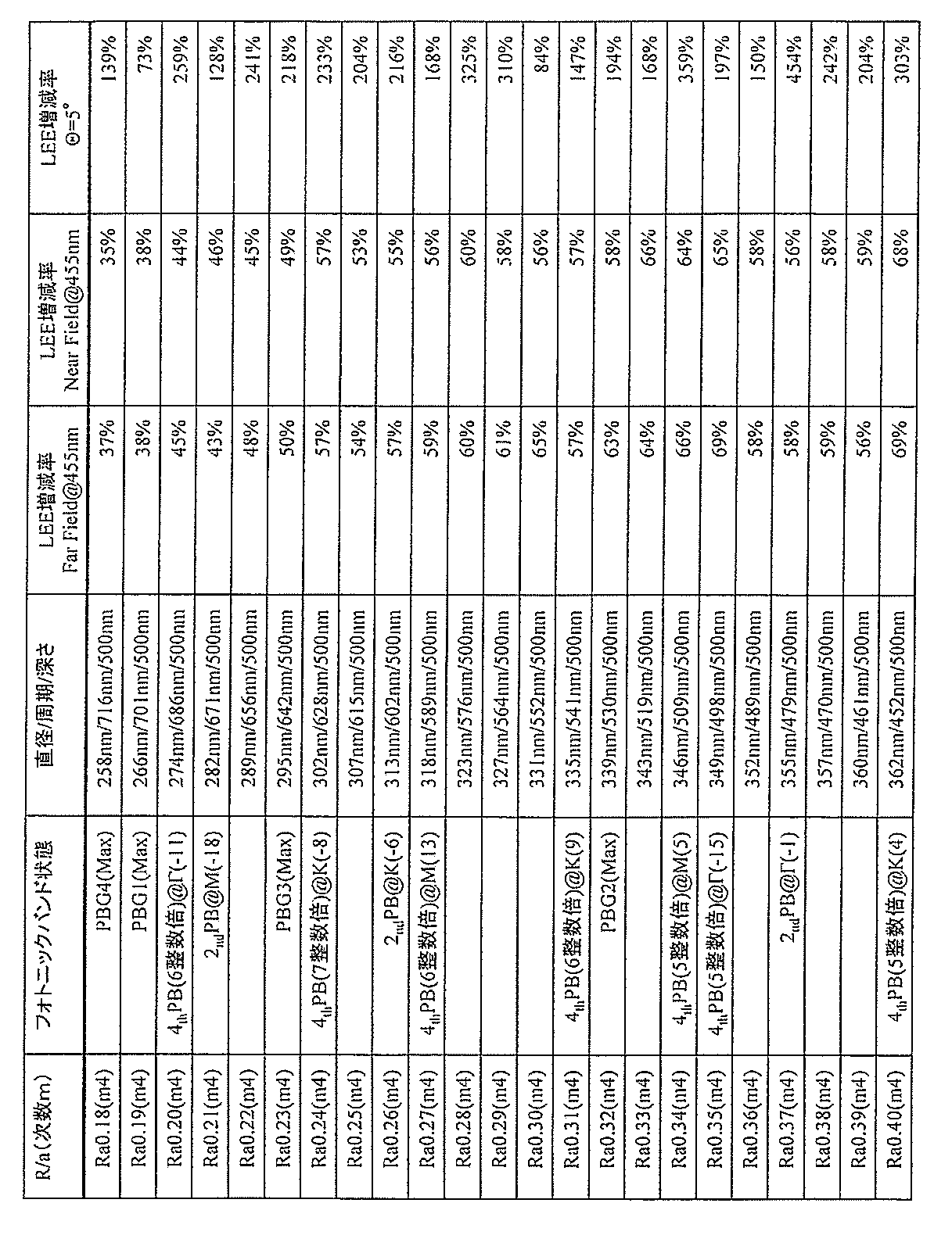
m=3及びm=4における各R/aについてFDTD法でシミュレーションした結果を、表1及び表2に記載する。LEE増減率(Far Field@455nm)とは遠方界にて計算された波長455nmにおけるLED素子の増減率を指す。LEE増減率(Near Field@455nm)とは近傍界にて計算された波長455nmにおけるLED素子の増減率を指す。LEE増減率(θ=5°)とは放射パターンのθ=5°における出力を0°≦φ≦360°の範囲で全て積分し、フォトニック結晶の有無で比較した増減率を指す。フォトニックバンド(PB)状態とはステップ3~6において求めたフォトニック結晶最適化の候補となる第二フォトニックバンド(2ndPB)と第四フォトニックバンド(4thPB)の各対称点における状態を示す。
また、各次数mにおける放射パターン角度分布を図14及び図15に示す。FDTD法では極座標にてθ方向並びにφ方向とも5°ステップで計算を実施している。この場合極座標上の各面積要素における光の強度はsinθdθdφで表現される。しかし、実際の配光性測定における検出器の面積は一定であるため両者の間には角度θの変化に伴い齟齬が生じる。従って、ここでは、縦軸の強度は単位面積当たりの相対出力で表示する。横軸に関しては角度θにおける出力を0°≦φ≦360°の範囲でφを全て積分して表示する。
(ステップS8)
光取出し効率(LEE)増減率が大きいR/aと次数mの中から、目的の配光性に相当するR/a及び次数mを選択する。従ってフォトニック結晶最適化のパラメータである、直径、周期、深さが決定される。ステップS3~S6で得られたフォトニック結晶最適化の候補となるR/aと0.18≦R/a≦0.40の範囲にある前記候補以外のR/aを比較する。結果としてS3~S6のステップで得られたR/aの最適化候補に落ち着く。
光取出し効率(LEE)増減率が大きいR/aと次数mの中から、目的の配光性に相当するR/a及び次数mを選択する。従ってフォトニック結晶最適化のパラメータである、直径、周期、深さが決定される。ステップS3~S6で得られたフォトニック結晶最適化の候補となるR/aと0.18≦R/a≦0.40の範囲にある前記候補以外のR/aを比較する。結果としてS3~S6のステップで得られたR/aの最適化候補に落ち着く。
表1及び表2より、LED素子のLEE増減率が65%以上で、例えば配光性の良さを表すθ=5°におけるLEE増減率が300%以上のR/a及びその次数mを選択してその放射パターン角度分布を図16に示す。また、PSS(Patterned Sapphire Substrate)に利用される以下の形状のミクロンパターンをFDTD法でシミュレーションして比較した。形状は側壁角度が60°のコーン型ピラー(上部/下部/周期/深さ)=(267nm/1200nm/1800nm/800nm)で、三角格子状に配置されている。図16から明らかなようにフォトニック結晶最適化の候補となるR/aはその他のR/aやミクロンパターンに比較して光取出し効率及び配光性とも良好との結果が得られた。特にR/a=0.34(次数m=4)のパターンがθ=0°~15°の上方において最も配光性の良い結果を示している。従ってステップS1からステップS8の処理を行えば、フォトニック結晶の光取出し効率と配光性を容易に最適化することができる。
尚、実際に製造する光半導体素子の構造を決める際には、最適化した値に基づいて決めることができるが、最適化した値そのものを用いなくても、それに近い値を用いた構造も本発明の範囲内に入るものである。
ところで、LEDの光はTE光とTM光が楕円偏光しながら媒質中を伝搬する。そこでフォトニック結晶に入射するTE光の様子についても以下に考察する。
図17に示すように、TE光の電界はフォトニック結晶面内に平行にピラー構造ロッド間に留まりやすく、平均屈折率nav、周期a及び設計波長λがブラッグ条件を満たす場合、その電界面においてブラッグ回折により反射される。TE光によるフォトニック結晶の物理的性質は前記TM光と同様なステップ(ステップS1~3)により次のマクスウエル方程式からフォトニックバンド(PB)構造を得て解析する。

但し、ε:比誘電率、G:逆格子ベクトル、k:波数、ω:周波数、c:光速、H:磁界である。
1stPB-2ndPB間、3rdPB-4thPB間、5thPB-6thPB間、7thPB-8thPB間のフォトニックバンドギャップ(PBG)を其々PBG1、PBG2、PBG3、PBG4とし、R/aとPBGの関係を図18に示す。
TM光のPBGと比較すると、TE光にはPBG1及びPBG2は存在しない。従ってこれらのフォトニックバンドでは定在波が存在せずTE光の反射効果は弱くなる。また、PBG3は0.28≦R/a≦0.39においてPBGが存在するが、その大きさはTM光のPBGと比較して非常に小さい。PBG4は0.20≦R/a≦0.25でPBGが存在するが、同様にその大きさは非常に小さい。但し、PBG3はR/a=0.34で、PBG4はR/a=0.22で僅かではあるが其々最大値が得られるので、最適化の有力候補となる。
次に、TM光のステップS4と同様に、ブラッグの条件を満たす第六フォトニックバンド(6thPB)と第八フォトニックバンド(8thPB)の縦軸を真空中の波長λVに換算し、次数m=1においてフォトニックバンド構造を得て図19及び図20に示す。何れのR/aも真空中の波長455nmに接近しないので定在波は生じない。また、次数m=3及び次数m=4においてTM光と同様(ステップS5~S6)な解析を行い、定在波を生じる条件を満たすフォトニックバンド構造を図21~図25に示す。最適化の有力候補はm=3の時、第六フォトニックバンドの5整数倍ではΓ点(R/a=0.33)、K点(R/a=0.36)、6整数倍ではM点(R/a=0.29)で、第八フォトニックバンドは該当しなかった。同様にm=4の時、第六フォトニックバンドの6整数倍では、Γ点(R/a=0.38)、7整数倍ではΓ点(R/a=0.31)、M点(R/a=0.35)、K点(R/a=0.32)、8整数倍ではM点(R/a=0.29)で、第八フォトニックバンドは該当しなかった。
TE光の解析で得られた最適化候補のR/aはフォトニック結晶によりLED内部に反射されるが、各PBGの大きさが小さく定在波を生じるエネルギーが小さいことからその反射効果はTM光の透過効果に比較して弱い。この事は次数m=3及びm=4において解析したFDTDの光取出し効率の増減率の結果とも良い一致を示していることからも理解できる。更に、サファイアC面に結晶成長したGaN系青色LEDの光はほとんどTE偏光されているので、本実施の形態によるFDTDの解析においても光源の偏光度を0.94とした。これはTE光の強度がTM光の10倍以上あり、一般にはTE光に有利なフォトニック結晶(ホール)を形成する場合が多い。しかし、解析結果ではフォトニック結晶(ピラー)の光取出し効率の増減率は非常に効果が高く、TE光やTM光に関係なく光取出し面の加工場所に応じてフォトニック結晶の構造を設計する事の重要性を示唆している。
そこで、平面波展開法で解析し、TE光においてPBGが最大となるR/a=0.40のホールを図26のようにGaN基板裏面に形成し、ピラーと同条件のFDTD法で光取出し効率の増減率の解析を実施した。但し、次数m=4、直径=407nm、周期=508nm、深さ=500nmで、設計波長455nmに対してブラッグの条件を満たしている。光取出し効率の増減率は65%という結果が得られた。この値は最適化されたピラー構造と比較して示唆通り若干劣化した。
次に、フォトニック結晶構造の製造方法について説明する。ナノインプリントは金型のフォトニック結晶パターンを基板上にスピンコートした有機レジストに大面積で一括転写する優れた技術を有する。また、樹脂フィルム金型を利用すれば基板が数百ミクロン程度反っていても転写が可能である。しかし、ナノインプリント用有機レジストは、流動性を重視するためにパターン被形成部である材料に対するエッチング選択比が必ずしも十分ではない。また、金型のパターンサイズとエッチング後のパターン被形成部サイズが一致しない。そこで、この問題を解決するために2層レジストを用いたプロセスを次のように実施する。
基板にエッチング選択比の大きい下層レジストを基板上にスピンコートするステップと、流動性と酸素耐性機能を有する上層レジストを前記下層レジストにスピンコートし、その上層にフォトニック結晶パターンを転写するステップと、前記パターン付き上層レジストを酸素プラズマに曝し酸素耐性を付与するステップと、前記酸素耐性を有したパターン付き上層レジストをマスクとして下層レジストを酸素プラズマでパターン形成を行うステップと、前記パターン付き下層レジストをマスクとして基板をICPプラズマでドライエッチングしてフォトニック結晶を形成する。
この方法であれば下層レジストの膜厚を変化させる事により、金型パターンの深さに対し2倍程度(GaNの場合)のエッチング深さを得ることが可能となる。また、上層レジストによる下層レジストのマスク形成時の酸素プラズマ条件を変化させる事により、金型パターンの直径に対し30%程度の直径調整をすることが可能となる。
より詳細な製造工程について説明する。良い光取出し効率を得るには、nmオーダーの加工を計算通りに形成する必要がある。
そこで、流動性とエッチング選択比の両方の特徴を兼ね備えた二層レジストを用いた、ナノインプリントリソグラフィー法による転写技術を用いて、nmオーダーの微細なパターンを有するフォトニック結晶周期構造を図27に示すとおり、一例として、GaN基板裏面に転写した。
設計波長をλとし、少なくとも、Al反射電極1と、p型GaN層5と、p型GaN発光層7と、をGaN基板15面とは反対側からこの順で含有する積層構造体を準備し、GaN基板15のAl反射電極1とは反対側にフォトニック結晶周期構造17を形成するための金型を準備し、GaN基板15面上に、レジスト層を形成し、金型の構造を転写し、レジスト層をマスクとしてGaN基板15面からエッチングしてフォトニック結晶周期構造17を形成する。これを、以下図27に沿って説明する。
はじめに、本発明の実施により最適化された周期構造を正確にGaN基板上に再現するための金型を作成する。この金型は、図27(b)に示すとおり基板の反りに追従できるよう樹脂製の金型を使用することもできる。
次に、GaN基板にエッチング選択比の大きい有機下層レジストを厚さgにてスピンコートする。なお、この厚さgは、GaN基板に対する下層レジストのエッチング選択比に応じて選択的に決定する。その後、下層レジスト面上に流動性と酸素耐性機能を有するシリコン含有上層レジストを所定の厚さにてスピンコートする(図27(a))。
次に、上層レジストに、金型のパターンを、ナノインプリント装置を用いて転写する(図27(b))。
次に、金型のパターンが転写された上層レジストを酸素プラズマに曝し、酸素耐性を付与するとともに、ナノインプリント転写において残存した上層レジストの残膜を除去する。(図27(c))。
次に、酸素耐性を有した上層レジストをマスクとして、有機下層レジストを酸素プラズマでエッチングし、GaN基板をドライエッチングするためのパターンマスクを形成する(図27(d))。なお、図27(e)に記載のパターンマスクのGaN基板側の直径d1は、酸素プラズマの条件を調整することで、d1の30%程度の範囲内で微調整することができる。
パターンマスクを介しICPプラズマでGaN基板をドライエッチングし、最適化された周期構造の形成がなされる(図27(e))。
周期構造がピラー構造による場合、エッチング後の形状は図27(f)に示すとおり概ねd1<d2の台形状となり、側壁角度は有機下層レジストのエッチング選択比に依存する。なお、本実施の形態によれば、有機下層レジストの厚さgを変更すれば、容易にドライエッチング後のGaN基板に形成するフォトニック結晶周期構造の深さを、金型の深さに対し1.5倍程度の深さとすることができる。
また、パターンマスク形成時に直径d1を変更すると、周期構造の直径を30%程度容易に変更することができる。これは、金型の作り直しに代えることが可能であり、金型の製作時間とコスト削減に寄与し、ひいては半導体発光素子の製造コスト上大きなメリットとなる。
処理および制御は、CPU(Central Processing Unit)やGPU(Graphics Processing Unit)によるソフトウェア処理、ASIC(Application Specific Integrated Circuit)やFPGA(Field Programmable Gate Array)によるハードウェア処理によって実現することができる。
また、上記の実施の形態において、添付図面に図示されている構成等については、これらに限定されるものではなく、本発明の効果を発揮する範囲内で適宜変更することが可能である。その他、本発明の目的の範囲を逸脱しない限りにおいて適宜変更して実施することが可能である。
また、本発明の各構成要素は、任意に取捨選択することができ、取捨選択した構成を具備する発明も本発明に含まれるものである。
また、本実施の形態で説明した機能を実現するためのプログラムをコンピュータ読み取り可能な記録媒体に記録して、この記録媒体に記録されたプログラムをコンピュータシステムに読み込ませ、実行することにより各部の処理を行ってもよい。尚、ここでいう「コンピュータシステム」とは、OSや周辺機器等のハードウェアを含むものとする。
また、「コンピュータシステム」は、WWWシステムを利用している場合であれば、ホームページ提供環境(あるいは表示環境)も含むものとする。
また、「コンピュータ読み取り可能な記録媒体」とは、フレキシブルディスク、光磁気ディスク、ROM、CD-ROM等の可搬媒体、コンピュータシステムに内蔵されるハードディスク等の記憶装置のことをいう。さらに「コンピュータ読み取り可能な記録媒体」とは、インターネット等のネットワークや電話回線等の通信回線を介してプログラムを送信する場合の通信線のように、短時間の間、動的にプログラムを保持するもの、その場合のサーバやクライアントとなるコンピュータシステム内部の揮発性メモリのように、一定時間プログラムを保持しているものも含むものとする。またプログラムは、前述した機能の一部を実現するためのものであっても良く、さらに前述した機能をコンピュータシステムにすでに記録されているプログラムとの組み合わせで実現できるものであっても良い。機能の少なくとも一部は、集積回路などのハードウェアで実現しても良い。
本明細書で引用した全ての刊行物、特許および特許出願をそのまま参考として本明細書にとり入れるものとする。
本発明は、半導体発光素子として利用可能である。
a:フォトニック結晶周期構造の周期、R:周期構造の半径、h:周期構造の加工深さ、1:Al反射電極(膜)、3:ITO透明電極、5:p-GaN層、7:発光層、11:n-GaN層、15:GaN基板、15a:界面、17a:GaNピラー構造、17b:空気、17:phc。
Claims (13)
- GaN基板の表面(側)に反射膜を有し、GaN基板裏面(側)に異なる屈折率を持つ2つの構造体からなるフォトニック結晶周期構造を有する半導体発光素子であって、
前記フォトニック結晶周期構造は、
真空中の設計波長λVと周期構造のパラメータである周期aと半径Rはブラッグの条件を満たし、
R/aが、
0.18から0.40までの範囲において、TM光のフォトニックバンド構造において2個のフォトニックバンドギャップを第四フォトニックバンド(4thPB)以内に有する半導体発光素子。 - 前記R/aは、
次数m=3又は4において各フォトニックバンドギャップの最大値に対応する値である請求項1に記載の半導体発光素子。 - 前記R/aは、
次数m=3又は4において、前記フォトニックバンド構造の縦軸(ωa/2πc)が真空中の波長λVに換算されたとき、第二フォトニックバンド(2ndPB)の対称点であるΓ点、M点、K点の何れかにおいて真空中の波長λV×mと点で接するか最も接近する値である請求項1に記載の半導体発光素子。 - 前記R/aは、
次数m=3のとき、前記フォトニックバンド構造の縦軸(ωa/2πc)の真空中の波長λV×3が、第四フォトニックバンド(4thPB)を4整数倍と5整数倍した各第四フォトニックバンド(4thPB)上の何れかの対称点と点で接するか最も接近する値である請求項1に記載の半導体発光素子。 - 前記R/aは、
次数m=4のとき、前記フォトニックバンド構造の縦軸(ωa/2πc)の真空中の波長λV×4が、第四フォトニックバンド(4thPB)を5整数倍、6整数倍、7整数倍した各第四フォトニックバンド(4thPB)上の何れかの対称点と点で接するか最も接近する値である請求項1に記載の半導体発光素子。 - 各周期構造のパラメータは、
選択された各R/aと0.5a以上の深さhからなるフォトニック結晶をFDTD法により計算し、光取出し効率と配光性とが最適化されるよう最終決定されたパラメータである請求項1から5までのいずれか1項に記載の半導体発光素子。 - 前記構造体は、
小さな屈折率の媒体中に大きい屈折率の構造を形成した構造体である請求項1から6までのいずれか1項に記載の半導体発光素子。 - 請求項1から7までのいずれか1項に記載の半導体発光素子におけるフォトニック結晶周期構造のパラメータ計算方法であって、
周期構造のパラメータである周期aと構造体の半径Rの比(R/a)を仮決定する第1ステップと、
構造体のそれぞれの屈折率n1とn2、及びこれらと前記R/aから平均屈折率navを算出し、これをブラッグ条件の式に代入し、次数m=3とm=4について、周期aと半径Rを得る第2ステップと、
前記R/a及び前記波長λ並びに前記屈折率n1、n2から得られる各構造体の誘電率ε1及びε2を用いた平面波展開法により、TM光のフォトニックバンド構造を解析する第3ステップと、
TM光の第二フォトニックバンド(2ndPB)と第四フォトニックバンド(4thPB)の縦軸(ωa/2πc)を真空中の波長λVに換算し、次数m=1においてλVとka/2πのフォトニックバンド構造を得る第4ステップと、
次数m=3及びm=4について、TM光の第二フォトニックバンド(2ndPB)と第四フォトニックバンド(4thPB)における各対称点における真空中の波長λV×mと点で接するか最も接近するR/aを求め、最適化の候補とする第5及び第6ステップと、 前記R/aに対応するフォトニック結晶の光取出し効率増減率と配光性を、0.18≦R/a≦0.40なる全てのR/aを次数m=3と4において有限時間領域差分法(FDTD法)で計算し、深さに関しては次数m=3~4において最も大きい周期aの0.5倍以上の任意の値を選択する第7ステップと、
を有することを特徴とするフォトニック結晶周期構造のパラメータ計算方法。 - 請求項1から7までのいずれか1項に記載の半導体発光素子におけるフォトニック結晶周期構造のパラメータ計算方法であって、
周期構造のパラメータである周期aと構造体の半径Rの比(R/a)を仮決定する第1ステップと、
構造体のそれぞれの屈折率n1とn2、及びこれらと前記R/aから平均屈折率navを算出し、これをブラッグ条件の式に代入し、次数m=3とm=4について、周期aと半径Rを得る第2ステップと、
前記R/a及び前記波長λ並びに前記屈折率n1、n2から得られる各構造体の誘電率ε1及びε2を用いた平面波展開法により、TM光のフォトニックバンド構造を解析する第3ステップと、
TM光の第二フォトニックバンド(2ndPB)と第四フォトニックバンド(4thPB)の縦軸(ωa/2πc)を真空中の波長λVに換算し、次数m=1においてλVとka/2πのフォトニックバンド構造を得る第4ステップと、
次数m=3及びm=4について、TM光の第二フォトニックバンド(2ndPB)と第四フォトニックバンド(4thPB)における各対称点における真空中の波長λV×mと点で接するか最も接近するR/aを求め、最適化の候補とする第5及び第6ステップと、 前記R/aに対応するフォトニック結晶の光取出し効率増減率と配光性を、0.18≦R/a≦0.40なる全てのR/aを次数m=3と4において有限時間領域差分法(FDTD法)で計算し、深さに関しては次数m=3~4において最も大きい周期aの0.5倍以上の任意の値を選択する第7ステップと、
光取出し効率(LEE)増減率が大きいR/aと次数mの中から、目的の配光性に相当するR/a及び次数mを選択し、直径、周期、深さが決定し、前記第3ステップから第6ステップまでで得られたフォトニック結晶最適化の候補となるR/aとその他のR/aを比較して配向性の良いパラメータを選択する第8ステップと、
を有することを特徴とするフォトニック結晶周期構造のパラメータ計算方法。 - 前記フォトニック結晶周期構造が、ナノインプリントリソグラフィー法による転写技術を用いて加工されたものであることを特徴とする請求項1に記載の半導体発光素子。
- 前記ナノインプリントリソグラフィー法による前記フォトニック結晶周期構造の転写が、加工対象の構造体に対しエッチング選択比の大きい下層レジストをコートし、その上に流動性と酸素耐性を有する上層レジストをコートする、二層レジスト法を用いた転写技術であることを特徴とする請求項10に記載の半導体発光素子。
- 半導体発光素子の製造方法であって、
設計波長をλとし、反射電極層と、p型GaN発光層と、をGaN基板面とは反対側からこの順で含有する積層構造体を準備する工程と、
前記GaN基板の前記反射電極層とは反対側にフォトニック結晶周期構造を形成するための金型を準備する工程と、
前記GaN基板面上に、レジスト層を形成し、前記金型の構造を転写する工程と、
前記レジスト層をマスクとして前記GaN基板面からエッチングしてフォトニック結晶周期構造を形成する工程と
を有する半導体発光素子の製造方法。 - 前記GaN基板面上に、レジスト層を形成し、前記金型の構造を転写する工程は、
前記GaN基板面上に、流動性の高い第1のレジスト層と、前記第1のレジスト層に対するエッチング選択比の高い第2のレジスト層と、による2層レジスト法を用いたドライエッチングを形成する工程と、
ナノインプリントリソグラフィー法を用いて前記第1のレジスト層に前記金型の構造を転写する工程と、を有し、
前記レジスト層をマスクとして順次前記GaN基板面をエッチングしてフォトニック結晶周期構造を形成する工程は、前記第1のレジスト層と前記第2のレジスト層とを、前記第2のレジスト層が露出するまでエッチングするとともに、前記第1のレジスト層のパターン凸部も合わせてエッチングし、
前記第2のレジスト層をマスクとして順次前記GaN基板面をエッチングしてフォトニック結晶周期構造を形成する工程を有することを特徴とする請求項12に記載の半導体発光素子の製造方法。
Applications Claiming Priority (2)
| Application Number | Priority Date | Filing Date | Title |
|---|---|---|---|
| JP2014248769 | 2014-12-09 | ||
| JP2014-248769 | 2014-12-09 |
Publications (1)
| Publication Number | Publication Date |
|---|---|
| WO2016093257A1 true WO2016093257A1 (ja) | 2016-06-16 |
Family
ID=56107434
Family Applications (1)
| Application Number | Title | Priority Date | Filing Date |
|---|---|---|---|
| PCT/JP2015/084461 WO2016093257A1 (ja) | 2014-12-09 | 2015-12-09 | 発光素子及びその製造方法 |
Country Status (2)
| Country | Link |
|---|---|
| TW (1) | TW201633559A (ja) |
| WO (1) | WO2016093257A1 (ja) |
Cited By (2)
| Publication number | Priority date | Publication date | Assignee | Title |
|---|---|---|---|---|
| JPWO2019146737A1 (ja) * | 2018-01-26 | 2021-01-07 | 丸文株式会社 | 深紫外led及びその製造方法 |
| CN116169200A (zh) * | 2023-04-26 | 2023-05-26 | 北京心灵方舟科技发展有限公司 | 一种近红外敏感硅光电倍增管及其制作工艺方法 |
Families Citing this family (1)
| Publication number | Priority date | Publication date | Assignee | Title |
|---|---|---|---|---|
| FR3068173B1 (fr) * | 2017-06-27 | 2020-05-15 | Aledia | Dispositif optoelectronique |
Citations (5)
| Publication number | Priority date | Publication date | Assignee | Title |
|---|---|---|---|---|
| JP2009033180A (ja) * | 2007-07-30 | 2009-02-12 | Samsung Electro Mech Co Ltd | 光子結晶発光素子及びその製造方法 |
| JP2009081469A (ja) * | 2003-07-16 | 2009-04-16 | Panasonic Corp | 半導体発光装置とこれを備えるモジュール |
| WO2013008556A1 (ja) * | 2011-07-12 | 2013-01-17 | 丸文株式会社 | 発光素子及びその製造方法 |
| US20130161677A1 (en) * | 2010-07-19 | 2013-06-27 | Rensselaer Polytechnic Institute | Integrated polarized light emitting diode with a built-in rotator |
| WO2013132993A1 (ja) * | 2012-03-07 | 2013-09-12 | 株式会社 アルバック | 素子の製造方法 |
-
2015
- 2015-12-09 TW TW104141362A patent/TW201633559A/zh unknown
- 2015-12-09 WO PCT/JP2015/084461 patent/WO2016093257A1/ja active Application Filing
Patent Citations (5)
| Publication number | Priority date | Publication date | Assignee | Title |
|---|---|---|---|---|
| JP2009081469A (ja) * | 2003-07-16 | 2009-04-16 | Panasonic Corp | 半導体発光装置とこれを備えるモジュール |
| JP2009033180A (ja) * | 2007-07-30 | 2009-02-12 | Samsung Electro Mech Co Ltd | 光子結晶発光素子及びその製造方法 |
| US20130161677A1 (en) * | 2010-07-19 | 2013-06-27 | Rensselaer Polytechnic Institute | Integrated polarized light emitting diode with a built-in rotator |
| WO2013008556A1 (ja) * | 2011-07-12 | 2013-01-17 | 丸文株式会社 | 発光素子及びその製造方法 |
| WO2013132993A1 (ja) * | 2012-03-07 | 2013-09-12 | 株式会社 アルバック | 素子の製造方法 |
Non-Patent Citations (6)
| Title |
|---|
| CHOI ET AL.: "Design of an LED Chip Structure with an Integrated Two-dimensional Photonic Crystal to Enhance the Light- extraction Efficiency", JOURNAL OF KOREAN PHYSICAL SOCIETY, vol. 94, no. 10, May 2014 (2014-05-01), pages 1425 - 1429 * |
| DING ET AL.: "Improving the Vertical Light- Extraction Efficiency of GaN-Based Thin-Film Flip-Chip LEDs With p-Side Deep-Hole Photonic Crystals", JOURNAL OF DISPLAY TECHNOLOGY, vol. 10, no. 11, November 2014 (2014-11-01), pages 909 - 916, XP011561975, DOI: doi:10.1109/JDT.2013.2281236 * |
| KASHIMA ET AL.: "The micro machining process technology of nano imprint and dry etcing to improve the efficiency of nitride LED", IEICE TECHNICAL REPORT, vol. 114, no. 336, 20 November 2014 (2014-11-20), pages 27 - 32 * |
| KIM ET AL.: "Enhancement of light extraction from GaN-based green light-emitting diodes using selective area photonic crystal", APPLIED PHYSICS LETTERS, vol. 96, 22 June 2010 (2010-06-22), pages 251103.1 - 251103.3 * |
| LAI ET AL.: "Directional light extraction enhancement from GaN-based film-transferred photonic crystal light-emitting diodes", APPLIED PHYSICS LETTERS, vol. 64, 25 March 2009 (2009-03-25), pages 123106 - 1 * |
| ORITA ET AL.: "High-Extraction-Efficiency Blue Light-Emitting Diode Using Extended-Pitch Photonic Crystal", JAPANESE JOURNAL OF APPLIED PHYSICS, vol. 43, no. 8B, 25 August 2004 (2004-08-25), pages 5809 - 5813 * |
Cited By (2)
| Publication number | Priority date | Publication date | Assignee | Title |
|---|---|---|---|---|
| JPWO2019146737A1 (ja) * | 2018-01-26 | 2021-01-07 | 丸文株式会社 | 深紫外led及びその製造方法 |
| CN116169200A (zh) * | 2023-04-26 | 2023-05-26 | 北京心灵方舟科技发展有限公司 | 一种近红外敏感硅光电倍增管及其制作工艺方法 |
Also Published As
| Publication number | Publication date |
|---|---|
| TW201633559A (zh) | 2016-09-16 |
Similar Documents
| Publication | Publication Date | Title |
|---|---|---|
| JP5315513B2 (ja) | 発光素子及びその製造方法 | |
| US9929317B2 (en) | Deep ultraviolet LED and method for manufacturing the same | |
| JP5967851B2 (ja) | フォトニック結晶周期構造のパラメータ計算方法、プログラム及び記録媒体 | |
| TWI523268B (zh) | Deep ultraviolet LED and its manufacturing method | |
| US10950751B2 (en) | Deep ultraviolet LED and method for manufacturing the same | |
| WO2016093257A1 (ja) | 発光素子及びその製造方法 | |
| TW201935715A (zh) | 深紫外線led及其製造方法 | |
| Liu et al. | Enhancing light extraction efficiency of GaN-based light-emitting diodes with reticulated photonic crystals | |
| Mercier et al. | Photonic crystal based control of directionality in GaN based LEDs |
Legal Events
| Date | Code | Title | Description |
|---|---|---|---|
| 121 | Ep: the epo has been informed by wipo that ep was designated in this application |
Ref document number: 15866653 Country of ref document: EP Kind code of ref document: A1 |
|
| NENP | Non-entry into the national phase |
Ref country code: DE |
|
| 122 | Ep: pct application non-entry in european phase |
Ref document number: 15866653 Country of ref document: EP Kind code of ref document: A1 |
|
| NENP | Non-entry into the national phase |
Ref country code: JP |